WO2017138091A1 - 光合波器 - Google Patents
光合波器 Download PDFInfo
- Publication number
- WO2017138091A1 WO2017138091A1 PCT/JP2016/053805 JP2016053805W WO2017138091A1 WO 2017138091 A1 WO2017138091 A1 WO 2017138091A1 JP 2016053805 W JP2016053805 W JP 2016053805W WO 2017138091 A1 WO2017138091 A1 WO 2017138091A1
- Authority
- WO
- WIPO (PCT)
- Prior art keywords
- light
- plane
- filter
- incident
- polarization
- Prior art date
Links
Images


Classifications
-
- G—PHYSICS
- G02—OPTICS
- G02B—OPTICAL ELEMENTS, SYSTEMS OR APPARATUS
- G02B6/00—Light guides; Structural details of arrangements comprising light guides and other optical elements, e.g. couplings
- G02B6/24—Coupling light guides
- G02B6/26—Optical coupling means
- G02B6/28—Optical coupling means having data bus means, i.e. plural waveguides interconnected and providing an inherently bidirectional system by mixing and splitting signals
- G02B6/293—Optical coupling means having data bus means, i.e. plural waveguides interconnected and providing an inherently bidirectional system by mixing and splitting signals with wavelength selective means
Definitions
- the present invention relates to an optical multiplexer that generates a wavelength-multiplexed optical signal by combining a plurality of lights.
- An optical multiplexer / demultiplexer is disclosed in Patent Document 1 as a conventional device that generates wavelength-multiplexed optical signals.
- the optical multiplexer / demultiplexer described in Patent Document 1 has an integrated zigzag configuration in which a wavelength selection filter having a dielectric multilayer film is attached to a filter substrate such as a glass block.
- the wavelength selection filter is a bandpass filter that transmits only a specific wavelength, and is formed by laminating a number of dielectric multilayer films in order to achieve separation from adjacent wavelengths.
- the present invention has been made in view of the above, and an object thereof is to obtain an optical multiplexer capable of realizing ease of manufacture and miniaturization.
- an optical multiplexer has a first plane and a second plane parallel to the first plane, and is incident on the first plane.
- First wavelength selection for reflecting the vertically polarized first light and transmitting the vertically polarized second light incident on the second plane and combining the first light and the second light Provide a filter.
- the optical multiplexer has a first plane and a second plane parallel to the first plane, reflects the horizontally polarized third light incident on the first plane, and reflects the second plane.
- a second wavelength selection filter that transmits the fourth light of the horizontally polarized light incident on the first light and combines the third light and the fourth light.
- the optical multiplexer has a first plane and a second plane parallel to the first plane, reflects vertically polarized light incident on the first plane and enters the second plane.
- a polarization selection filter that transmits horizontally polarized light and combines vertically polarized light and horizontally polarized light is provided. Further, in the optical multiplexer, the first light and the second light are not adjacent on the frequency axis, and the third light and the fourth light are not adjacent on the frequency axis, The first light and the second light combined by the first wavelength selective filter enter the first plane of the polarization selective filter, and the second wavelength selective filter enters the second plane of the polarization selective filter. The third light and the fourth light that are combined in the step enter.
- the optical multiplexer according to the present invention has an effect that it can be easily manufactured and can be downsized.
- 1 is a diagram illustrating a configuration example of an optical multiplexer according to a first embodiment.
- 1 is a diagram illustrating a configuration example of an optical multiplexing module according to a first embodiment.
- route after the light of (lambda) 1 injects into the optical multiplexing module concerning Embodiment 1 and radiate
- FIG. The figure which shows the function of the polarization rotator concerning Embodiment 1.
- FIG. 4 The figure which shows the structure and operation
- FIG. The figure which shows the structure and operation
- FIG. The figure which shows the relationship of the wavelength of each light which the optical multiplexing module concerning Embodiment 5 combines.
- FIG. 1 is a diagram illustrating a configuration example of an optical multiplexer according to a first embodiment of the present invention.
- the optical multiplexer 1 according to the present embodiment includes an optical path changing unit 10 that outputs a plurality of lights having different wavelengths input from the outside in an arbitrary order, and a plurality of optical paths that are output from the optical path changing unit 10. And an optical multiplexing module 20 that combines and outputs the light.
- the light input to the optical multiplexer 1 is assumed to be TE (Transverse Electric) mode light, that is, horizontally polarized light.
- the TE mode light input to the optical multiplexer 1 is light output from a light source that is a laser diode.
- the light path changing unit 10 is realized by combining a reflecting plate, a filter that transmits light of a specific wavelength, and the like, and changes the paths of a plurality of light incident from the incident surface and emits the light.
- light having wavelengths ⁇ 1, ⁇ 2, ⁇ 3, and ⁇ 4 is incident on the optical path changing unit 10, and the optical path changing unit 10 changes the light path having the wavelength ⁇ 2 and the light path having the wavelength ⁇ 3.
- the light beams having wavelengths ⁇ 1, ⁇ 2, ⁇ 3, and ⁇ 4 are emitted after the order is changed.
- the optical path changing unit 10 may multiplex light having wavelengths adjacent to each other on the frequency axis in the same wavelength selection filter among a plurality of wavelength selection filters described later. Rearrange the light of each wavelength so that there is no.
- the optical multiplexing module 20 combines and emits a plurality of incident lights.
- FIG. 1 shows an example in which the optical multiplexing module 20 combines and emits light having wavelengths ⁇ 1 to ⁇ 4.
- the wavelength may be indicated only by “ ⁇ n” (n is a positive integer).
- FIG. 2 is a diagram illustrating the relationship of the wavelengths of the lights combined by the optical multiplexing module 20 according to the first embodiment.
- ⁇ 1 is the longest and ⁇ 4 is the shortest.
- ⁇ 1 1309.14 nm
- ⁇ 2 1304.58 nm
- ⁇ 3 1300.05 nm
- ⁇ 4 1295.56 nm are used.
- the frequency is arranged at intervals of 800 GHz. This corresponds to the standard 100GBASE-LR4 defined by IEEE (The Institute of Electrical and Electronics Engineers).
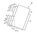
- FIG. 3 is a diagram illustrating a configuration example of the optical multiplexing module 20 according to the first embodiment.
- the optical multiplexing module 20 includes a filter holder 21, a total reflection mirror 22, a dummy filter 23, WDM (Wavelength Division Multiplex) filters 24-1 and 24-2, which are wavelength selection filters, a polarization rotator 25, A polarization selection filter 26.
- WDM Widelength Division Multiplex
- the filter holder 21 is formed of a light transmitting member, such as glass, and has an outer shape that is a rectangular parallelepiped.
- a total reflection mirror 22, a dummy filter 23, a WDM filter 24-1 and a polarization selection filter 26 are attached to the filter holder 21.
- the total reflection mirror 22 is fixed to the first surface which is a specific surface of the filter holder 21.
- the dummy filter 23, the WDM filter 24-1, and the polarization selection filter 26 are fixed to a second surface parallel to the first surface of the filter holder 21.
- the distance from the first surface to the second surface is “a”.
- the outer shape of the filter holder 21 is described as a rectangular parallelepiped, it is an example.
- the filter holder 21 may have any shape as long as it has two parallel planes.
- the filter holder 21 does not have wavelength selection performance and transmits all wavelengths.
- the total reflection mirror 22 has a reflection surface that is a flat surface that reflects light of all wavelengths without having wavelength selection performance, and this reflection surface is fixed to the first surface of the filter holder 21.
- the reflection surface of the total reflection mirror 22 reflects light incident from the filter holder 21 side.
- the reflection surface of the total reflection mirror 22 is narrower than the first surface of the filter holder 21, and a part of the first surface of the filter holder 21 is not covered with the total reflection mirror 22.
- the reflection surface of the total reflection mirror 22 and the first surface of the filter holder 21 are fixed in a state in which one end of each is aligned. A portion of the first surface of the filter holder 21 that is not covered with the total reflection mirror 22 forms a light output portion 28. The light traveling in the filter holder 21 is emitted from the light output unit 28 to the outside.
- the dummy filter 23 has two parallel planes, that is, a first plane 23A and a second plane 23B parallel to the first plane 23A, and the first plane 23A is fixed to the second plane of the filter holder 21. Yes.
- the dummy filter 23 does not have wavelength selection performance, and emits as it is when light is incident from the outside.
- the distance from the first plane 23A to the second plane 23B of the dummy filter 23 is “b”.
- the WDM filter 24-1 has two parallel planes, that is, a first plane 24-1A and a second plane 24-1B parallel to the first plane 24-1A.
- the first plane 24-1A is the filter holder 21. Is fixed to the second surface.
- the WDM filter 24-1 is a band-pass filter that has wavelength selection performance, transmits light of a specific wavelength, and reflects light other than the specific wavelength.
- the specific wavelength is ⁇ 3.
- the distance from the first plane 24-1A to the second plane 24-1B of the WDM filter 24-1 is “b”.
- the polarization selection filter 26 has two parallel planes, that is, a first plane 26A and a second plane 26B parallel to the first plane 26A, and the first plane 26A is fixed to the second surface of the filter holder 21. Has been.
- the polarization selection filter 26 transmits light having a specific polarization and reflects light other than the specific polarization.
- the specific polarization is assumed to be a TE mode, that is, a horizontal polarization.
- the distance from the first plane 26A to the second plane 26B of the polarization selection filter 26 is “b”.
- the WDM filter 24-1 is disposed between the dummy filter 23 and the polarization selection filter 26. Further, the polarization selection filter 26 is disposed at a position closer to the light output unit 28 than the WDM filter 24-1.
- the polarization rotator 25 has two parallel planes, that is, a first plane 25A and a second plane 25B parallel to the first plane 25A.
- the first plane 25A is the second plane 23B of the dummy filter 23.
- the WDM filter 24-1 is fixed to the second plane 24-1B.
- the polarization rotator 25 has a polarization rotation function for changing the polarization state of incident light. When TE mode light is incident, it is converted into TM (Transverse Magnetic) mode light, that is, vertically polarized light. And exit.
- the polarization rotator 25 can be realized using a half-wave plate. The distance from the first plane 25A to the second plane 25B of the polarization rotator 25 is assumed to be “c”.
- the WDM filter 24-2 has two parallel planes, that is, a first plane 24-2A and a second plane 24-2B parallel to the first plane 24-2A, and the first plane 24-2A is polarization selection.
- the filter 26 is fixed to the second plane 26B.
- the WDM filter 24-2 is a bandpass filter that has wavelength selection performance, transmits light of a specific wavelength, and reflects light other than the specific wavelength.
- the specific wavelength is ⁇ 4.
- the distance from the first plane 24-2A to the second plane 24-2B of the WDM filter 24-2 is assumed to be “c”.
- the filter holder 21, the dummy filter 23, the WDM filters 24-1 and 24-2, the polarization rotator 25, and the polarization selection filter 26 are all configured with the same refractive index n2.
- Each component of the filter holder 21, the dummy filter 23, the WDM filters 24-1 and 24-2, the polarization rotator 25, and the polarization selection filter 26 is formed by stacking a dielectric multilayer film on a material having a refractive index n2. Configured. For example, when glass is used, the refractive index n2 is about 1.5. Strictly speaking, the refractive index of the dielectric multilayer filter constituting each constituent element is different from the refractive index of glass, but can be approximately ignored.
- Filter effects in each of the dummy filter 23, the WDM filter 24-1, and the polarization selection filter 26 are obtained on the first plane in contact with the filter holder 21. Further, the filter effect in the WDM filter 24-2 is obtained on the first plane in contact with the polarization selection filter 26.
- the incident light to the optical multiplexing module 20 is a parallel beam, that is, collimated light, and incident light of all wavelengths has an incident angle ⁇ 1 with respect to the incident surface of the optical multiplexing module 20, and an incident angle ⁇ 2 inside the optical multiplexing module 20. It is arranged to become.
- the incident angle ⁇ 1 and the incident angle ⁇ 2 are related by Snell's law.
- the incident surface of the optical multiplexing module 20 is the second plane 25B of the polarization rotator 25, the second plane 24-2B of the WDM filter 24-2, or the second plane 26B of the polarization selection filter 26.
- the inside of the optical multiplexing module 20 is the inside of the incident surface of the optical multiplexing module 20, that is, the inside of the second plane 25B of the polarization rotator 25, the inside of the second plane 24-2B of the WDM filter 24-2, or It is inside the second plane 26 ⁇ / b> B of the polarization selection filter 26.
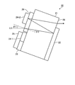
- FIG. 4 is a diagram illustrating a path from the time when the light of ⁇ 1 enters the optical multiplexing module 20 to the time of emission.
- the light of ⁇ 1 enters the polarization rotator 25, is converted from the TE mode light to the TM mode light, and then enters the dummy filter 23. Since the dummy filter 23 transmits all wavelengths, the light of ⁇ 1 passes through the dummy filter 23 and enters the filter holder 21.
- TE mode light is indicated by a solid line
- TM mode light is indicated by a broken line.
- the light of ⁇ 1 After being incident on the filter holder 21, the light of ⁇ 1 is reflected by the total reflection mirror 22, further reflected by the WDM filter 24-1, and then again reflected by the total reflection mirror 22. Then, the light of wavelength ⁇ 1 is reflected a plurality of times between the polarization selection filter 26 and the total reflection mirror 22, and then emitted from the light output unit 28.
- FIG. 5 is a diagram showing a path from the incident of the light of ⁇ 3 to the optical multiplexing module 20 until the emission.
- the light of ⁇ 3 enters the polarization rotator 25, is converted from the TE mode light to the TM mode light, and then enters the WDM filter 24-1. Since the WDM filter 24-1 transmits ⁇ 3, the light of ⁇ 3 passes through the WDM filter 24-1 and enters the filter holder 21.
- TE mode light is indicated by a solid line
- TM mode light is indicated by a broken line.
- FIG. 6 is a diagram illustrating a path from the time when the light having the wavelength ⁇ 2 is incident on the optical multiplexing module 20 until the light is emitted.
- the light of ⁇ 2 enters the polarization selection filter 26. Since the polarization selection filter 26 has a characteristic of transmitting the TE mode light, the light of ⁇ 2 that is the TE mode light passes through the polarization selection filter 26 and enters the filter holder 21. After being incident on the filter holder 21, the light of ⁇ ⁇ b> 2 is reflected by the total reflection mirror 22 and enters the polarization selection filter 26.
- the polarization selection filter 26 transmits the light of ⁇ 2 and enters the WDM filter 24-2.
- the WDM filter 24-2 transmits ⁇ 4 light and reflects light of other wavelengths, the ⁇ 2 light is reflected by the WDM filter 24-2.
- the light of ⁇ 2 reflected by the WDM filter 24-2 passes through the polarization selection filter 26, enters the filter holder 21, and then exits from the light output unit 28.
- FIG. 7 is a diagram illustrating a path from the time when the light having the wavelength ⁇ 4 is incident on the optical multiplexing module 20 until the light is emitted.
- the light of ⁇ 4 enters the WDM filter 24-2. Since the WDM filter 24-2 transmits ⁇ 4, the light of ⁇ 4 passes through the WDM filter 24-2 and enters the polarization selection filter 26. Since the polarization selection filter 26 has a characteristic of transmitting TE mode light, the light of ⁇ 4, which is TE mode light, incident on the polarization selection filter 26 passes through the polarization selection filter 26 and the filter holder 21. Is incident on. The light of ⁇ 4 enters the filter holder 21 and is then emitted from the light output unit 28.
- FIG. 8 is a diagram illustrating the operation of the optical multiplexing module 20.
- light arranged in the order of ⁇ 1, ⁇ 3, ⁇ 2, and ⁇ 4 enters the optical multiplexing module 20.
- the polarization rotator 25 changes the polarization state from the TE mode to the TM mode.
- the TE mode light is indicated by a solid line
- the TM mode light is indicated by a broken line.
- Each of the light of ⁇ 1, ⁇ 3, and ⁇ 2 incident on the optical multiplexing module 20 is repeatedly reflected between the total reflection mirror 22 and the WDM filter 24-1, the polarization selection filter 26, or the WDM filter 24-2.
- the light is output to the light output unit 28. Further, the light of ⁇ 4 is guided to the light output unit 28 without being reflected. While being guided to the optical output unit 28, the light of each wavelength is multiplexed or multiplexed with the light of other wavelengths. As a result, a plurality of light in a wavelength multiplexed state is emitted from the light output unit 28.
- FIG. 9 is a diagram showing the function of the polarization rotator 25. As shown in the figure, the ⁇ 1 light and the ⁇ 3 light are incident on the polarization rotator 25, and the polarization rotator 25 converts the incident ⁇ 1 light and ⁇ 3 light from the TE mode to the TM mode.
- FIG. 10 is a diagram illustrating the function of the WDM filter 24-1 which is the first wavelength selection filter. As shown in the figure, light of ⁇ 1 and light of ⁇ 3 are incident on the first wavelength selection filter, and the first wavelength selection filter combines the incident light of ⁇ 1 and light of ⁇ 3.
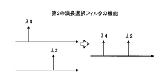
- FIG. 11 is a diagram showing the function of the WDM filter 24-2 as the second wavelength selection filter. As shown in the figure, light of ⁇ 2 and light of ⁇ 4 are incident on the second wavelength selection filter, and the second wavelength selection filter multiplexes the incident light of ⁇ 2 and light of ⁇ 4.
- FIG. 12 is a diagram illustrating the function of the polarization selection filter 26.
- the polarization selective filter 26 is a state in which the first wavelength multiplexed light in which the light of ⁇ 1 and the light of ⁇ 3 are multiplexed, the light of ⁇ 2 and the light of ⁇ 4 are multiplexed.
- the second wavelength multiplexed light is incident, and the polarization selective filter 26 multiplexes the incident first wavelength multiplexed light and the second wavelength multiplexed light to obtain the light of ⁇ 1 and the light of ⁇ 2.
- ⁇ 3 light and ⁇ 4 light are multiplexed to generate wavelength multiplexed light.
- the optical multiplexing module 20 in order for the optical multiplexing module 20 to generate the wavelength multiplexed light in which the light of each wavelength of ⁇ 1 to ⁇ 4 is multiplexed, the light of each wavelength of ⁇ 1 to ⁇ 4 is emitted from the optical multiplexing module 20. It is necessary to pass through the same position of the light output unit 28. If light of all wavelengths is emitted from the same position of the light output unit 28, the incident light pitches P1, P2, and P3 shown in FIG. 8 use the dimensions a, b, and c shown in FIG. It is determined by the following equation (1).
- the light of these two wavelengths enters the polarization rotator 25 and is converted from the TE mode to the TM mode when passing through the polarization rotator 25.
- the light of ⁇ 1 that has passed through the polarization rotator 25 passes through the dummy filter 23 that does not have wavelength selection performance, and is reflected by the total reflection mirror 22.
- a WDM filter that transmits ⁇ 1 may be provided. Thereafter, in the WDM filter 24-1 that selectively transmits only ⁇ 3, the light of ⁇ 1 and the light of ⁇ 3 are multiplexed.
- the WDM filter 24-1 transmits the light of ⁇ 3 incident on the second plane 24-1B, emits the light from the first plane 24-1A, and emits the light of ⁇ 1 incident on the first plane 24-1A. Is reflected, the light of ⁇ 1 that is the first light and the light of ⁇ 3 that is the second light are multiplexed. The ⁇ 1 light and the ⁇ 3 light traveling on the same optical path after being combined are reflected between the total reflection mirror 22 and the polarization selective filter 26 that transmits the TE mode light and reflects the TM mode light. Then, the light output unit 28 is reached.
- Light of these wavelengths travels in the optical multiplexing module 20 in the TE mode.
- the light of ⁇ 2 enters the polarization selection filter 26 that transmits the TE mode light, and passes through the polarization selection filter 26.
- the light of ⁇ 4 enters the WDM filter 24-2 that selectively transmits only the light of ⁇ 4, and passes through the WDM filter 24-2.
- the light of ⁇ 2 that has passed through the polarization selection filter 26 and entered the filter holder 21 is reflected by the total reflection mirror 22. Thereafter, ⁇ 2 and ⁇ 4 are combined in the WDM filter 24-2 that selectively transmits only the light of ⁇ 4.
- the WDM filter 24-2 transmits the light of ⁇ 4 incident on the second plane 24-2B, exits from the first plane 24-2A, and emits the light of ⁇ 2 incident on the first plane 24-2A. Is reflected, and the light of ⁇ 2 that is the third light and the light of ⁇ 4 that is the fourth light are multiplexed.
- the incident position of the light of each wavelength so as to satisfy the formula (1) showing the relationship between P1, P2, and P3, the incident light of all wavelengths is multiplexed, and the light output unit 28.
- the WDM filter 24-1 and the WDM filter 24-2 are assumed to be bandpass filters that selectively transmit only specific wavelengths, but edge filters that transmit or block only a certain wavelength or more are assumed. It may be used.
- the optical multiplexing module 20 includes the first wavelength selection filter and the second wavelength selection filter, and each wavelength selection filter reflects without passing through.
- the optical path changing unit 10 does not allow the light that enters the wavelength selection filters from the first plane and the light that enters from the second plane to be adjacent to each other on the frequency axis. That is, in other words, the arrangement order of the light of each wavelength is changed so that the interval on the frequency axis between wavelengths combined by each wavelength selection filter is increased.
- the optical path changing unit 10 can be omitted.
- the light source is set so that the order of arrangement of each light incident on the optical multiplexing module 20 is a desired order.
- the desired order is the order in which the light combined by the wavelength selection filter, that is, the light transmitted through the wavelength selection filter and the reflected light are not adjacent to each other on the frequency axis.
- optical multiplexer 1 When the optical multiplexer 1 according to the present embodiment is used, it is possible to simultaneously form an optical multiplexer with a structure that can be integrally molded and easily reduce the required accuracy of the WDM filter as follows.
- the optical multiplexer 1 does not need to combine adjacent wavelengths such as ⁇ 1 and ⁇ 2 with a WDM filter, a band-pass filter having a sharp edge required for the optical multiplexer / demultiplexer described in Patent Document 1 is provided. This is unnecessary, and can be realized with a WDM filter having a smaller number of dielectric layers than the WDM filter required by the optical multiplexer / demultiplexer described in Patent Document 1. As a result, the WDM filter can be easily manufactured and the stress caused by the dielectric layer stacking can be reduced, so that an optical multiplexer having stable characteristics can be realized.
- the optical multiplexing module 20 of the optical multiplexer 1 since the WDM filter does not combine adjacent wavelengths, an allowable deviation of the filter wavelength characteristic with respect to the variation in the incident angle can be increased. Therefore, the optical multiplexing module 20 can be realized with a larger incident angle, and as a result, the optical multiplexer 1 can be miniaturized.
- Embodiment 2 In the optical multiplexer 1 according to the first embodiment, the ⁇ 1 light and the ⁇ 3 light are converted from the TE mode to the TM mode. However, the ⁇ 2 light and the ⁇ 4 light are converted from the TE mode to the TM mode. However, the same effect can be obtained.
- the polarization rotator 25 is disposed on the optical path of the light of ⁇ 2 and the optical path of the light of ⁇ 4, and the polarization selection filter 26 has a characteristic of reflecting the TE mode and transmitting the TM mode.
- the characteristics of the WDM filters 24-1 and 24-2 are the same as those in the first embodiment.
- the pitches P1, P2, and P3 of light of each wavelength incident on the dummy filter 23, the WDM filter 24-1, or the polarization rotator 25 are determined by the incident angle of each incident light and the filter holder 21.
- the distance a from the first surface to the second surface, and the first to second planes in each of the dummy filter 23, the WDM filters 24-1 and 24-2, the polarization rotator 25, and the polarization selection filter To the distances b and c.
- Embodiment 3 FIG.
- the polarization rotator 25 is fixed to the filter holder 21 via the dummy filter 23, the WDM filter 24-2, etc., but the polarization rotator 25 is fixed to the filter holder 21. You may arrange
- the polarization rotator 25 has only a mode conversion function and does not reflect light.
- Embodiment 4 FIG.
- the WDM filters 24-1 and 24-2 and the polarization selection filter 26 of the optical multiplexers of Embodiments 1 to 3 have characteristics that can obtain a filter effect on the first plane, but the filter effect on the second plane. May be obtained.
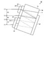
- FIG. 13 is a diagram illustrating the configuration and operation of the optical multiplexing module provided in the optical multiplexer according to the fourth embodiment.
- the optical multiplexing module 20a according to the fourth embodiment includes the WDM filters 24-1 and 24-2 and the polarization selection filter 26 of the optical multiplexing module 20 described in the first embodiment, and the WDM filters 24a-1 and 24a-2.
- the configuration is replaced with the polarization selection filter 26a.
- the WDM filters 24a-1 and 24a-2 and the polarization selection filter 26a have the same size and the same arrangement as the WDM filters 24-1 and 24-2 and the polarization selection filter 26, respectively.
- the optical multiplexing module 20a has the same configuration as that of the optical multiplexing module 20 of the first embodiment except for the WDM filters 24a-1, 24a-2 and the polarization selection filter 26a. In this embodiment, parts different from those in Embodiment 1 will be described. As shown in the drawing, the WDM filters 24a-1 and 24a-2 and the polarization selection filter 26a reflect light in the second plane instead of the first plane when light having a wavelength that is reflected without being transmitted is incident.
- FIG. 13 shows an optical path of ⁇ 1 light and an optical path of ⁇ 2 as an example.
- the light of ⁇ 3 passes through the polarization rotator 25 and then enters the second plane of the WDM filter 24a-1, where it is combined with the light of ⁇ 1.
- the light of ⁇ 4 is incident on the second plane of the WDM filter 24a-2, where it is combined with the light of ⁇ 2. All wavelengths of light are combined in the second plane of the polarization selective filter 26a.
- some of the WDM filters 24a-1, 24a-2 and the polarization selection filter 26a may be filters having the same characteristics as those in the first embodiment. That is, you may mix the thing of the characteristic which can obtain the filter effect in the 1st plane, and the thing which can obtain the filter effect in the 2nd plane.
- the length a ′ of the filter holder 21 can be shortened, and the optical multiplexing module 20a can be downsized. Further downsizing of the optical multiplexer can be realized.
- Embodiment 5 FIG. In the first to fourth embodiments, an optical multiplexer that combines four wavelengths is described. In this embodiment, an optical multiplexer that combines eight wavelengths is described.
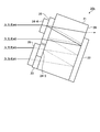
- FIG. 14 is a diagram illustrating a configuration example and an operation example of the optical multiplexing module provided in the optical multiplexer according to the fifth embodiment.
- the optical multiplexing module 20b according to the fifth embodiment has a configuration in which the WDM filters 24-1 and 24-2 of the optical multiplexing module 20 described in the first embodiment are replaced with WDM filters 24-3 and 24-4.
- the WDM filters 24-3 and 24-4 have the same size and the same arrangement as the WDM filters 24-1 and 24-2.
- the optical multiplexing module 20b has the same configuration as that of the first embodiment except for the WDM filters 24-3 and 24-4. In this embodiment, parts different from those in Embodiment 1 will be described.
- the TE mode light is indicated by a solid line
- the TM mode light is indicated by a broken line.
- FIG. 15 is a diagram illustrating a relationship between wavelengths of lights combined by the optical multiplexing module 20b according to the fifth embodiment.
- the light of ⁇ 1 and the light of ⁇ 2 shown in FIG. 15 constitute the input light # 1 to the optical multiplexing module 20b
- the light of ⁇ 3 and the light of ⁇ 4 constitute the input light # 2 to the optical multiplexing module 20b
- ⁇ 5 The light of ⁇ 6 and the light of ⁇ 6 constitute the input light # 3 to the optical multiplexing module 20b
- the light of ⁇ 7 and the light of ⁇ 8 constitute the input light # 4 to the optical multiplexing module 20b. That is, the optical multiplexing module 20b combines four optical signals in a state where two waves have already been combined.
- Each input light to the optical multiplexing module 20b is generated by, for example, an integrated laser in which two semiconductor lasers operating at different wavelengths and a multiplexer for multiplexing two wavelengths are integrated on a semiconductor chip.
- the WDM filter 24-3 selectively transmits input light # 3, that is, light of ⁇ 5 and light of ⁇ 6, and reflects light of other wavelengths.
- the WDM filter 24-4 has a characteristic of selectively transmitting the input light # 4, that is, the light of ⁇ 7 and the light of ⁇ 8 and reflecting the light of other wavelengths.
- the light of ⁇ 1 and the light of ⁇ 2 enter the filter holder 21 as the input light # 1 through the polarization rotator 25 and the dummy filter 23, and the light of ⁇ 5 and the light of ⁇ 6 Enters the filter holder 21 via the polarization rotator 25 and the WDM filter 24-3 as input light # 3.
- These input lights # 1 and # 3 enter the filter holder 21 in the TM mode.
- the light of ⁇ 3 and the light of ⁇ 4 enter the filter holder 21 as the input light # 2 through the polarization selection filter 26, and the light of ⁇ 7 and the light of ⁇ 8 enter the WDM filter 24-4 and the polarization as the input light # 4.
- the light enters the filter holder 21 through the wave selection filter 26.
- These input lights # 2 and # 4 enter the filter holder 21 in the TE mode.
- Each input light after entering the filter holder 21 is reflected by the total reflection mirror 22 and reflected or transmitted by each filter in the same manner as the light of ⁇ 1 to ⁇ 4 described in the first embodiment, and has eight wavelengths.
- An optical signal in a state of being combined is generated.
- the input light # 1 and the input light # 3 are incident on the first plane and the second plane of the wavelength selection filter 24-3 as the first light and the second light, respectively.
- the wavelength selection filter 24-3 reflects the light incident on the first plane and transmits the light incident on the second plane to multiplex these lights.
- the input light # 2 and the input light # 4 are incident on the first plane and the second plane of the wavelength selection filter 24-4 as the third light and the fourth light, respectively.
- the wavelength selection filter 24-4 reflects the light incident on the first plane and transmits the light incident on the second plane to multiplex these lights.
- the light obtained by combining the input light # 1 and the input light # 3 and the light obtained by combining the input light # 1 and the input light # 3 are the first plane and the second plane of the polarization selection filter 26. Respectively.
- the polarization selective filter 26 multiplexes these lights by reflecting the light incident on the first plane and transmitting the light incident on the second plane.
- the optical multiplexer / demultiplexer described in Patent Document 1 requires a WDM filter that separates adjacent wavelengths.
- the wavelength range to be selected that is, the range of transmitted wavelengths is 2 while keeping the edge of the WDM filter. Therefore, it is extremely difficult to manufacture a WDM filter.
- the wavelength selection range required for the WDM filter is doubled, but the edge can be set gently, and the filter can be easily manufactured. .
- the optical multiplexer / demultiplexer using multiple reflection shown in Patent Document 1 can realize multiplexing of many wavelengths such as 8 waves in principle by increasing the number of reflections, considering manufacturing tolerances of members, etc. It is desirable to have 4 waves or less.
- the WDM filters 24-3 and 24-4 are similar to the WDM filter 24a-1 described in the fourth embodiment and the like, in the second plane, that is, the plane with the longer distance from the total reflection mirror 22. It is good also as a characteristic which performs reflection.
- the same effect can be obtained when the interval between wavelengths to be combined is set to an interval other than 800 GHz.
- Embodiment 6 FIG.
- an optical multiplexer that performs multiplexing on light that is arranged at equal intervals with all wavelengths of 800 GHz has been described.
- the optical multiplexer described in the fifth embodiment can also multiplex with light partially arranged at unequal intervals.
- the interval between ⁇ 4 and ⁇ 5 is 1.6 THz, which is a double frequency compared to other wavelength intervals.
- This document has been proposed at the IEEE P802.3bs 400 GbE standardization meeting.
- the configuration disclosed in this document corresponds to a structure in which ⁇ 5 to ⁇ 8 are shifted by 800 GHz to the short wavelength side among the eight wavelengths ⁇ 1 to ⁇ 8 shown in FIG.
- the wavelength interval between the ⁇ 4 light and the ⁇ 7 light combined by the WDM filter 24-4 shown in FIG. 4 is 800 GHz larger than 2.4 THz when the wavelength interval between the ⁇ 4 light and the ⁇ 5 light is 800 GHz.
- the required specification for the WDM filter can be further relaxed.
- the wavelengths to be multiplexed by the optical multiplexer of the fifth embodiment are unequal, but in the optical multiplexers of the first to fourth embodiments, the wavelengths to be multiplexed are also determined. It is possible to have unequal intervals.
- the configuration described in the above embodiment shows an example of the contents of the present invention, and can be combined with another known technique, and can be combined with other configurations without departing from the gist of the present invention. It is also possible to omit or change the part.
- optical multiplexer 10 optical path changing unit, 20, 20a, 20b optical multiplexing module, 21 filter holder, 22 total reflection mirror, 23 dummy filter, 24-1, 24-2, 24-3, 24-4, 24a -1,24a-2 WDM filter, 25 polarization rotator, 26 polarization selection filter, 23A, 24-1A, 24-2A, 25A, 26A first plane, 23B, 24-1B, 24-2B, 25B , 26B second plane, 28 light output section.
Landscapes
- Physics & Mathematics (AREA)
- General Physics & Mathematics (AREA)
- Optics & Photonics (AREA)
- Optical Couplings Of Light Guides (AREA)
- Polarising Elements (AREA)
Abstract
光合波器は、第1の平面に入射した垂直偏波の第1の光を反射するとともに第2の平面に入射した垂直偏波の第2の光を透過して第1の光と第2の光とを合波するWDMフィルタ(24-1)、第1の平面に入射した水平偏波の第3の光を反射するとともに第2の平面に入射した水平偏波の第4の光を透過して第3の光と第4の光とを合波するWDMフィルタ(24-2)、第1の平面に入射した垂直偏波の光を反射するとともに第2の平面に入射した水平偏波の光を透過して垂直偏波の光と水平偏波の光とを合波する偏波選択フィルタ(26)、を備え、第1の光と第2の光とは周波数軸上で隣接しておらず、かつ第3の光と第4の光とは周波数軸上で隣接しておらず、偏波選択フィルタ(26)の第1の平面にWDMフィルタ(24-1)で合波された光が入射し、偏波選択フィルタ(26)の第2の平面にWDMフィルタ(24-2)で合波された光が入射する。
Description
本発明は、複数の光を合波して波長多重された光信号を生成する光合波器に関する。
波長多重された光信号を生成する従来の機器として、光合分波器が特許文献1で開示されている。特許文献1に記載の光合分波器は、誘電体多層膜を形成した波長選択フィルタが、ガラスブロック等のフィルタ基板に張り付けられた、一体型のジグザグ型の構成とされている。波長選択フィルタは特定の波長のみを透過するバンドパスフィルタであり、隣接波長との分離を実現するため、多数の誘電体多層膜を積層して形成される。
特許文献1に記載の光合分波器においては、波長選択フィルタが隣接する波長同士を対象として分波または合波を行うため、波長選択フィルタに求められる性能が厳しく、製造が困難という課題がある。具体的には、隣接する波長同士を分離させるためにはエッジの鋭いバンドパスフィルタが必要である。しかし、そのようなフィルタ特性を実現するためには、フィルタを構成する誘電体層の数を増やす必要があり、応力による特性劣化が生じる可能性があるという問題があった。加えて、隣接する波長との十分な波長分離をするためには、入射角度を小さくする必要があり、光合分波器が大きくなるという問題があった。
本発明は、上記に鑑みてなされたものであって、製造の容易性および小型化を実現可能な光合波器を得ることを目的とする。
上述した課題を解決し、目的を達成するために、本発明にかかる光合波器は、第1の平面および第1の平面に平行な第2の平面を有し、第1の平面に入射した垂直偏波の第1の光を反射するとともに第2の平面に入射した垂直偏波の第2の光を透過して第1の光と第2の光とを合波する第1の波長選択フィルタを備える。また、光合波器は、第1の平面および第1の平面に平行な第2の平面を有し、第1の平面に入射した水平偏波の第3の光を反射するとともに第2の平面に入射した水平偏波の第4の光を透過して第3の光と第4の光とを合波する第2の波長選択フィルタを備える。また、光合波器は、第1の平面および第1の平面に平行な第2の平面を有し、第1の平面に入射した垂直偏波の光を反射するとともに第2の平面に入射した水平偏波の光を透過して垂直偏波の光と水平偏波の光とを合波する偏波選択フィルタを備える。さらに、光合波器において、第1の光と第2の光とは周波数軸上で隣接しておらず、かつ第3の光と第4の光とは周波数軸上で隣接しておらず、偏波選択フィルタの第1の平面に第1の波長選択フィルタで合波された第1の光および第2の光が入射し、偏波選択フィルタの第2の平面に第2の波長選択フィルタで合波された第3の光および第4の光が入射する。
本発明にかかる光合波器は、製造の容易性および小型化を実現できるという効果を奏する。
以下に、本発明の実施の形態にかかる光合波器を図面に基づいて詳細に説明する。なお、この実施の形態によりこの発明が限定されるものではない。
実施の形態1.
図1は、本発明の実施の形態1にかかる光合波器の構成例を示す図である。本実施の形態にかかる光合波器1は、外部から入力された波長が異なる複数の光を任意の順番に並べ替えて出力する光経路変更部10と、光経路変更部10から出力された複数の光を合波して出力する光合波モジュール20とを備える。光合波器1に入力される光はTE(Transverse Electric)モードの光、すなわち水平偏波の光であるものとする。光合波器1に入力されるTEモードの光は、レーザダイオードである光源から出力された光とする。
図1は、本発明の実施の形態1にかかる光合波器の構成例を示す図である。本実施の形態にかかる光合波器1は、外部から入力された波長が異なる複数の光を任意の順番に並べ替えて出力する光経路変更部10と、光経路変更部10から出力された複数の光を合波して出力する光合波モジュール20とを備える。光合波器1に入力される光はTE(Transverse Electric)モードの光、すなわち水平偏波の光であるものとする。光合波器1に入力されるTEモードの光は、レーザダイオードである光源から出力された光とする。
光経路変更部10は、反射板、特定波長の光を透過するフィルタなどを組み合わせて実現され、入射面より入射された複数の光の経路を変更して出射する。図1では、波長がλ1,λ2,λ3,λ4の光が光経路変更部10に入射し、光経路変更部10は波長がλ2の光の経路と波長がλ3の光の経路とを変更して順番を入れ替えた上で波長がλ1,λ2,λ3,λ4の各光を出射する例を示している。光経路変更部10は、後段の光合波モジュール20において、周波数軸上で隣接している波長の光同士が、後述する複数の波長選択フィルタの中の同じ波長選択フィルタにおいて合波されることがないように、各波長の光を並べ替える。
光合波モジュール20は、入射された複数の光を合波して出射する。図1では、光合波モジュール20が、波長がλ1~λ4の光を合波して出射する例を示している。なお、以下の説明では「λn」(nは正の整数)のみで波長を示す場合がある。
図2は、実施の形態1にかかる光合波モジュール20が合波する各光の波長の関係を示す図である。図2に示したように、本実施の形態ではλ1が最も長く、λ4が最も短いものとする。4つの波長としては、λ1=1309.14nm、λ2=1304.58nm、λ3=1300.05nm、λ4=1295.56nmといった波長が用いられる。周波数は800GHz間隔の配置とする。これはIEEE(The Institute of Electrical and Electronics Engineers)で規定されている100GBASE-LR4という規格に対応する。
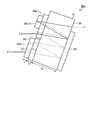
図3は、実施の形態1にかかる光合波モジュール20の構成例を示す図である。光合波モジュール20は、フィルタホルダ21と、全反射ミラー22と、ダミーフィルタ23と、波長選択フィルタであるWDM(Wavelength Division Multiplex)フィルタ24-1および24-2と、偏波回転器25と、偏波選択フィルタ26と、を備える。
フィルタホルダ21は光を透過する部材、例えばガラスで形成され、その外形は直方体とする。フィルタホルダ21には全反射ミラー22、ダミーフィルタ23、WDMフィルタ24-1および偏波選択フィルタ26が取り付けられている。具体的には、全反射ミラー22がフィルタホルダ21の特定の面である第1面に固着されている。ダミーフィルタ23、WDMフィルタ24-1および偏波選択フィルタ26がフィルタホルダ21の第1面と平行な第2面に固着されている。第1面から第2面までの距離を「a」とする。なお、ここではフィルタホルダ21の外形を直方体として説明するが一例である。フィルタホルダ21は、互いに平行な2つの平面を有する形状であればどのような形状であってもよい。フィルタホルダ21は波長選択性能を有しておらず、全ての波長を透過する。
全反射ミラー22は、波長選択性能を有さずに全ての波長の光を反射する平面である反射面を有し、この反射面がフィルタホルダ21の第1面に固着されている。全反射ミラー22の反射面はフィルタホルダ21側から入射する光を反射する。全反射ミラー22の反射面はフィルタホルダ21の第1面よりも狭く、フィルタホルダ21の第1面の一部分は全反射ミラー22で覆われていない。全反射ミラー22の反射面とフィルタホルダ21の第1面とは、お互いの一端同士を揃えた状態で固着されている。フィルタホルダ21の第1面のうち、全反射ミラー22で覆われていない部分が光出力部28を形成している。フィルタホルダ21内を進んだ光は、光出力部28から外部へ出射される。
ダミーフィルタ23は、平行な2つの平面、すなわち、第1の平面23Aとこれに平行な第2の平面23Bとを有し、第1の平面23Aがフィルタホルダ21の第2面に固着されている。ダミーフィルタ23は、波長選択性能を有しておらず、外部から光が入射すると、そのまま出射する。ダミーフィルタ23の第1の平面23Aから第2の平面23Bまでの距離を「b」とする。
WDMフィルタ24-1は、平行な2つの平面、すなわち、第1の平面24-1Aとこれに平行な第2の平面24-1Bとを有し、第1の平面24-1Aがフィルタホルダ21の第2面に固着されている。WDMフィルタ24-1は、波長選択性能を有しており、特定波長の光を透過し、特定波長以外の光については反射するバンドパスフィルタである。ここでは、特定波長をλ3とする。WDMフィルタ24-1の第1の平面24-1Aから第2の平面24-1Bまでの距離を「b」とする。
偏波選択フィルタ26は、平行な2つの平面、すなわち、第1の平面26Aとこれに平行な第2の平面26Bとを有し、第1の平面26Aがフィルタホルダ21の第2面に固着されている。偏波選択フィルタ26は特定偏波の光を透過し、特定偏波以外の光については反射する。ここでは、特定偏波をTEモードすなわち水平偏波とする。偏波選択フィルタ26の第1の平面26Aから第2の平面26Bまでの距離を「b」とする。
WDMフィルタ24-1は、ダミーフィルタ23と偏波選択フィルタ26との間に配置されている。また、偏波選択フィルタ26は、WDMフィルタ24-1よりも光出力部28に近い位置に配置されている。
偏波回転器25は、平行な2つの平面、すなわち、第1の平面25Aとこれに平行な第2の平面25Bとを有し、第1の平面25Aがダミーフィルタ23の第2の平面23BおよびWDMフィルタ24-1の第2の平面24-1Bに固着されている。偏波回転器25は、入射された光の偏波状態を変更する偏波回転機能を有し、TEモードの光が入射するとTM(Transverse Magnetic)モードの光すなわち垂直偏波の光に変換して出射する。偏波回転器25は、1/2波長板を利用して実現できる。偏波回転器25の第1の平面25Aから第2の平面25Bまでの距離を「c」とする。
WDMフィルタ24-2は、平行な2つの平面、すなわち、第1の平面24-2Aとこれに平行な第2の平面24-2Bとを有し、第1の平面24-2Aが偏波選択フィルタ26の第2の平面26Bに固着されている。WDMフィルタ24-2は、波長選択性能を有しており、特定波長の光を透過し、特定波長以外の光については反射するバンドパスフィルタである。ここでは、特定波長をλ4とする。WDMフィルタ24-2の第1の平面24-2Aから第2の平面24-2Bまでの距離を「c」とする。
ここで、フィルタホルダ21、ダミーフィルタ23、WDMフィルタ24-1,24-2、偏波回転器25および偏波選択フィルタ26は、全て同じ屈折率n2で構成される。フィルタホルダ21、ダミーフィルタ23、WDMフィルタ24-1,24-2、偏波回転器25および偏波選択フィルタ26の各構成要素は、屈折率n2の材料に対し、誘電体多層膜を積層して構成される。例えばガラスを使用した場合、屈折率n2は約1.5となる。厳密には各構成要素を構成する誘電体多層膜フィルタの屈折率はガラスの屈折率とは異なるが、近似的に無視出来る。ダミーフィルタ23、WDMフィルタ24-1および偏波選択フィルタ26の各々におけるフィルタ効果は、フィルタホルダ21と接している第1の平面で得られる。また、WDMフィルタ24-2におけるフィルタ効果は、偏波選択フィルタ26と接している第1の平面で得られる。光合波モジュール20の外は屈折率n1=1の空気で満たされている。
また、光合波モジュール20への入射光は並行ビームすなわちコリメート光であり、全ての波長の入射光は、光合波モジュール20の入射面に対し入射角θ1、光合波モジュール20の内側では入射角θ2となるよう配置される。ここで入射角θ1と入射角θ2とはスネルの法則で関係づけられる。光合波モジュール20の入射面とは、偏波回転器25の第2の平面25B、WDMフィルタ24-2の第2の平面24-2Bまたは偏波選択フィルタ26の第2の平面26Bである。光合波モジュール20の内側とは、光合波モジュール20の入射面の内側、すなわち偏波回転器25の第2の平面25Bの内側、WDMフィルタ24-2の第2の平面24-2Bの内側または偏波選択フィルタ26の第2の平面26Bの内側である。
図4は、光合波モジュール20にλ1の光が入射してから出射するまでの経路を示す図である。λ1の光は、偏波回転器25に入射し、TEモードの光からTMモードの光に変換された後、ダミーフィルタ23に入射する。ダミーフィルタ23は全ての波長を透過するため、λ1の光は、ダミーフィルタ23を通過してフィルタホルダ21に入射する。図4では、TEモードの光を実線、TMモードの光を破線で示している。λ1の光はフィルタホルダ21に入射した後、全反射ミラー22で反射され、さらに、WDMフィルタ24-1で反射された後、再度全反射ミラー22で反射される。そして、波長λ1の光は偏波選択フィルタ26と全反射ミラー22との間で複数回反射された後、光出力部28から出射される。
図5は、光合波モジュール20にλ3の光が入射してから出射するまでの経路を示す図である。λ3の光は、偏波回転器25に入射し、TEモードの光からTMモードの光に変換された後、WDMフィルタ24-1に入射する。WDMフィルタ24-1はλ3を透過する特性のため、λ3の光は、WDMフィルタ24-1を通過してフィルタホルダ21に入射する。図5では、図4と同様に、TEモードの光を実線、TMモードの光を破線で示している。λ3の光はフィルタホルダ21に入射した後、全反射ミラー22で反射され、さらに、偏波選択フィルタ26と全反射ミラー22との間で複数回反射された後、光出力部28から出射される。
図6は、光合波モジュール20にλ2の光が入射してから出射するまでの経路を示す図である。λ2の光は、偏波選択フィルタ26に入射する。偏波選択フィルタ26はTEモードの光を透過する特性のため、TEモードの光であるλ2の光は、偏波選択フィルタ26を通過してフィルタホルダ21に入射する。λ2の光はフィルタホルダ21に入射した後、全反射ミラー22で反射され、偏波選択フィルタ26に入射する。偏波選択フィルタ26はλ2の光を透過し、WDMフィルタ24-2に入射する。WDMフィルタ24-2はλ4の光を透過し、その他の波長の光は反射する特性のため、λ2の光は、WDMフィルタ24-2で反射される。WDMフィルタ24-2で反射されたλ2の光は偏波選択フィルタ26を通過してフィルタホルダ21に入射した後、光出力部28から出射される。
図7は、光合波モジュール20にλ4の光が入射してから出射するまでの経路を示す図である。λ4の光は、WDMフィルタ24-2に入射する。WDMフィルタ24-2はλ4を透過する特性のため、λ4の光は、WDMフィルタ24-2を通過して偏波選択フィルタ26に入射する。偏波選択フィルタ26はTEモードの光を透過する特性であるため、偏波選択フィルタ26に入射した、TEモードの光であるλ4の光は、偏波選択フィルタ26を通過してフィルタホルダ21に入射する。λ4の光はフィルタホルダ21に入射した後、光出力部28から出射される。
図8は、光合波モジュール20の動作を示す図である。図8に示したように、光合波モジュール20にはλ1、λ3、λ2およびλ4の順番に並べられた光が入射する。このとき、λ1およびλ3については、偏波回転器25において偏波状態がTEモードからTMモードに変更される。図8では、図4および図5と同様に、TEモードの光を実線、TMモードの光を破線で示している。光合波モジュール20に入射したλ1、λ3およびλ2の光の各々は、全反射ミラー22と、WDMフィルタ24-1、偏波選択フィルタ26またはWDMフィルタ24-2との間で反射が繰り返されて光出力部28に導かれる。また、λ4の光は反射されることなく光出力部28に導かれる。各波長の光は、光出力部28に導かれている間に他の波長の光と多重化すなわち合波される。この結果、波長多重された状態の複数の光が光出力部28から出射される。
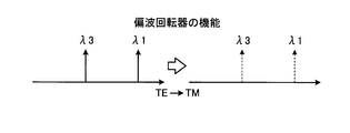
図9は、偏波回転器25の機能を示す図である。図示したように、偏波回転器25にはλ1の光およびλ3の光が入射し、偏波回転器25は、入射したλ1の光およびλ3の光をTEモードからTMモードに変換する。
図10は、第1の波長選択フィルタであるWDMフィルタ24-1の機能を示す図である。図示したように、第1の波長選択フィルタにはλ1の光およびλ3の光が入射し、第1の波長選択フィルタは、入射したλ1の光とλ3の光とを合波する。
図11は、第2の波長選択フィルタであるWDMフィルタ24-2の機能を示す図である。図示したように、第2の波長選択フィルタにはλ2の光およびλ4の光が入射し、第2の波長選択フィルタは、入射したλ2の光とλ4の光とを合波する。
図12は、偏波選択フィルタ26の機能を示す図である。図示したように、偏波選択フィルタ26には、λ1の光とλ3の光とが多重化された状態の第1の波長多重化光と、λ2の光とλ4の光とが多重された状態の第2の波長多重化光とが入射し、偏波選択フィルタ26は、入射した第1の波長多重化光と第2の波長多重化光とを合波し、λ1の光、λ2の光、λ3の光およびλ4の光が多重化された状態の波長多重化光を生成する。
ここで、光合波モジュール20がλ1~λ4の各波長の光が多重化された状態の波長多重化光を生成するためには、λ1~λ4の各波長の光が光合波モジュール20から出射される際に光出力部28の同じ位置を通過する必要がある。全ての波長の光を光出力部28の同じ位置から出射させようとすると、図8に示した入射光のピッチP1,P2,P3は、図3に示した寸法a,b,cを用い、以下の式(1)で決まる。
P1=2a×tanθ2×cosθ1
P2=2(a-b)×tanθ2×cosθ1-c×tanθ2
P3=2(a+b)×tanθ2×cosθ1+c×tanθ2 …(1)
P2=2(a-b)×tanθ2×cosθ1-c×tanθ2
P3=2(a+b)×tanθ2×cosθ1+c×tanθ2 …(1)
例えば、θ2=6度、基準の入射光ピッチP1=1.20mm、b=1.00mm、c=1.00mm、n1=1、n2=1.5とした場合、a=5.78mm、θ1=9.02度、P2=0.89mm、P3=1.51mmとなる。ピッチに着目すると、P1=1.2mm、P2=0.89mm、P3=1.51mmと、不等間隔になる。これはλ2の光が光合波モジュール20に入射してから最初に反射するまでの距離すなわち入射位置から全反射ミラー22までの距離、およびλ2の光の反射位置すなわちλ2の光を反射するフィルタが他の波長の光と異なるためである。
次に、光合波モジュール20がλ1~λ4の各波長の光を合波する動作について、図8を参照しながら説明する。
まず、λ1およびλ3に注目する。この2つの波長の光は偏波回転器25に入射し、偏波回転器25を通過する際にTEモードからTMモードに変換される。偏波回転器25を通過したλ1の光は、波長選択性能を有さないダミーフィルタ23を通過し、全反射ミラー22で反射する。なお、ダミーフィルタ23に代えて、λ1を透過するWDMフィルタを備えるようにしてもよい。その後、λ3のみを選択的に透過するWDMフィルタ24-1において、λ1の光とλ3の光との合波が行われる。すなわち、WDMフィルタ24-1は、第2の平面24-1Bに入射したλ3の光を透過して第1の平面24-1Aから出射し、第1の平面24-1Aに入射したλ1の光を反射することにより、第1の光であるλ1の光と第2の光であるλ3の光とを合波する。合波されて同一光路上を進むλ1の光およびλ3の光は、全反射ミラー22と、TEモードの光を透過するとともにTMモードの光を反射する偏波選択フィルタ26との間を反射しながら進み、光出力部28に至る。
次に、λ2およびλ4に注目する。これら波長の光は光合波モジュール20内をTEモードで進む。λ2の光は、TEモードの光を透過する偏波選択フィルタ26に入射し、偏波選択フィルタ26を通過する。λ4の光は、λ4の光のみを選択的に透過するWDMフィルタ24-2に入射し、WDMフィルタ24-2を通過する。偏波選択フィルタ26を通過してフィルタホルダ21に入射したλ2の光は全反射ミラー22で反射する。その後、λ4の光のみを選択的に透過するWDMフィルタ24-2において、λ2とλ4の合波が行われる。すなわち、WDMフィルタ24-2は、第2の平面24-2Bに入射したλ4の光を透過して第1の平面24-2Aから出射し、第1の平面24-2Aに入射したλ2の光を反射することにより、第3の光であるλ2の光と第4の光であるλ4の光とを合波する。ここで、前述のP1,P2,P3の関係を示した式(1)を満たすように各波長の光の入射位置を調整する事で、入射した全波長の光が合波され、光出力部28から出射される。
本実施の形態において、WDMフィルタ24-1およびWDMフィルタ24-2は特定の波長のみを選択的に透過するバンドパスフィルタを想定しているが、ある波長以上のみを透過あるいは遮断するエッジフィルタを用いてもよい。
このように、本実施の形態にかかる光合波器1において、光合波モジュール20は、第1の波長選択フィルタおよび第2の波長選択フィルタを備え、各波長選択フィルタは、透過せずに反射する光である第1の平面から入射する光と、透過する光である第2の平面から入射する光とが、周波数軸上で隣り合った波長同士とならない組み合わせの光、すなわち、合波する波長同士の周波数軸上での間隔が大きくなる組み合わせの光を対象として合波を行う。また、光合波器1において、光経路変更部10は、各波長選択フィルタに第1の平面から入射する光と第2の平面から入射する光とが周波数軸上で隣り合った波長同士とならないように、すなわち、各波長選択フィルタで合波する波長同士の周波数軸上での間隔が大きくなるように、各波長の光の並び順を変更する。
なお、光合波器1が合波する光が、出射する光の波長を変更可能な光源、例えばチューナブルレーザーから発光される場合、光経路変更部10を省略することができる。光経路変更部10を省略した場合、光合波モジュール20に入射する各光の並び順が所望の順番となるように光源を設定する。所望の順番とは、波長選択フィルタで合波される光、すなわち、波長選択フィルタを透過する光と反射する光とが周波数軸上で隣り合った波長同士とならない順番とする。
本実施形態にかかる光合波器1を用いる場合、部材の角度精度が出しやすい一体成型可能な構成での光合波器形成と、以下に示すWDMフィルタへの要求精度緩和とが同時に可能となる。
光合波器1は上記のλ1とλ2のような隣接する波長同士をWDMフィルタで合波する必要が無いため、特許文献1に記載された光合分波器で必要なエッジの鋭いバンドパスフィルタが不要となり、特許文献1に記載された光合分波器が必要とするWDMフィルタよりも少ない数の誘電体層のWDMフィルタで実現出来る。これによりWDMフィルタの製造が容易になるとともに誘電体層積層による応力を小さくする事ができ、安定した特性の光合波器を実現できる。
また、WDMフィルタへの光の入射角が大きくなると、入射角のずれに対してフィルタ波長特性のずれが大きくなる。本実施の形態にかかる光合波器1の光合波モジュール20では、WDMフィルタが隣接波長同士の合波を行わないため、入射角のバラつきに対するフィルタ波長特性の許容ずれを大きく取ることができる。よって、より大きな入射角で光合波モジュール20を実現でき、その結果、光合波器1の小型化が可能となる。
実施の形態2.
実装の形態1にかかる光合波器1では、λ1の光およびλ3の光をTEモードからTMモードに変換することとしたが、λ2の光およびλ4の光をTEモードからTMモードに変換するようにしても同様の効果が得られる。この場合、λ2の光の光路およびλ4の光の光路上に偏波回転器25を配置し、偏波選択フィルタ26はTEモードを反射し、かつTMモードを透過する特性とする。WDMフィルタ24-1および24-2の特性は実施の形態1と同様とする。
実装の形態1にかかる光合波器1では、λ1の光およびλ3の光をTEモードからTMモードに変換することとしたが、λ2の光およびλ4の光をTEモードからTMモードに変換するようにしても同様の効果が得られる。この場合、λ2の光の光路およびλ4の光の光路上に偏波回転器25を配置し、偏波選択フィルタ26はTEモードを反射し、かつTMモードを透過する特性とする。WDMフィルタ24-1および24-2の特性は実施の形態1と同様とする。
ダミーフィルタ23、WDMフィルタ24-1または偏波回転器25に入射する各波長の光のピッチP1,P2,P3は、実施の形態1と同様に、各入射光の入射角と、フィルタホルダ21の第1面から第2面までの距離aと、ダミーフィルタ23、WDMフィルタ24-1,24-2、偏波回転器25および偏波選択フィルタの各々における第1の平面から第2の平面までの距離b,cと、に基づいて求められる。
実施の形態3.
実施の形態1,2においては、偏波回転器25をダミーフィルタ23、WDMフィルタ24-2などを介してフィルタホルダ21に固定することとしたが、偏波回転器25をフィルタホルダ21に固定せずに個別に配置してもよい。この場合、フィルタホルダ21に対して張り付ける部材が少なくて済むため、光合波器1の作製が容易となる。偏波回転器25はモード変換機能のみを有し、光を反射させない。ミラー等を個別に固定する場合、張り付け時の角度ずれが生じると多重反射させた場合のビーム角度のずれにつながるため許容実装誤差が厳しいが、モード変換機能のみを有する偏波回転器25はビーム角度ずれに寄与しないため、固定時の角度ずれに対する許容誤差が大きく、個別に配置しても特性が不安定になる可能性は低い。
実施の形態1,2においては、偏波回転器25をダミーフィルタ23、WDMフィルタ24-2などを介してフィルタホルダ21に固定することとしたが、偏波回転器25をフィルタホルダ21に固定せずに個別に配置してもよい。この場合、フィルタホルダ21に対して張り付ける部材が少なくて済むため、光合波器1の作製が容易となる。偏波回転器25はモード変換機能のみを有し、光を反射させない。ミラー等を個別に固定する場合、張り付け時の角度ずれが生じると多重反射させた場合のビーム角度のずれにつながるため許容実装誤差が厳しいが、モード変換機能のみを有する偏波回転器25はビーム角度ずれに寄与しないため、固定時の角度ずれに対する許容誤差が大きく、個別に配置しても特性が不安定になる可能性は低い。
実施の形態4.
実施の形態1~3の光合波器のWDMフィルタ24-1,24-2および偏波選択フィルタ26は、第1の平面でフィルタ効果が得られる特性としたが、第2の平面でフィルタ効果が得られる特性としてもよい。
実施の形態1~3の光合波器のWDMフィルタ24-1,24-2および偏波選択フィルタ26は、第1の平面でフィルタ効果が得られる特性としたが、第2の平面でフィルタ効果が得られる特性としてもよい。
図13は、実施の形態4にかかる光合波器が備えている光合波モジュールの構成および動作を示す図である。実施の形態4にかかる光合波モジュール20aは、実施の形態1で説明した光合波モジュール20のWDMフィルタ24-1,24-2および偏波選択フィルタ26をWDMフィルタ24a-1,24a-2および偏波選択フィルタ26aに置き換えた構成である。WDMフィルタ24a-1,24a-2および偏波選択フィルタ26aの各フィルタは、それぞれ、WDMフィルタ24-1,24-2および偏波選択フィルタ26と同じサイズかつ同じ配置とする。光合波モジュール20aは、WDMフィルタ24a-1,24a-2および偏波選択フィルタ26a以外の構成については実施の形態1の光合波モジュール20と同様である。本実施の形態では実施の形態1と異なる部分について説明を行う。図示したように、WDMフィルタ24a-1,24a-2および偏波選択フィルタ26aは、透過せずに反射する波長の光が入射した場合、第1の平面ではなく第2の平面において反射する。
図13では、一例として、λ1の光の光路およびλ2の光の光路を示している。λ3の光は、偏波回転器25を通過した後、WDMフィルタ24a-1の第2の平面に入射し、そこでλ1の光と合波される。λ4の光は、WDMフィルタ24a-2の第2の平面に入射し、そこでλ2の光と合波される。偏波選択フィルタ26aの第2の平面において全ての波長の光が合波される。
なお、WDMフィルタ24a-1,24a-2および偏波選択フィルタ26aのうち、一部を実施の形態1と同様の特性のフィルタとしてもよい。すなわち、第1の平面でフィルタ効果が得られる特性のものと第2の平面でフィルタ効果が得られるものとを混在させてもよい。例えば、図13に示した偏波選択フィルタ26aを偏波選択フィルタ26に置き換えた構成としてもよい。
本実施の形態の光合波器によれば、各フィルタにおける反射点が全反射ミラー22から遠くなるため、フィルタホルダ21の長さa’を短くする事ができ、光合波モジュール20aを小型化でき、光合波器のさらなる小型化を実現できる。
実施の形態5.
実施の形態1~4では、4波の波長を合波する光合波器について説明したが、本実施の形態では、8波の波長を合波する光合波器を説明する。
実施の形態1~4では、4波の波長を合波する光合波器について説明したが、本実施の形態では、8波の波長を合波する光合波器を説明する。
図14は、実施の形態5にかかる光合波器が備えている光合波モジュールの構成例および動作例を示す図である。実施の形態5にかかる光合波モジュール20bは、実施の形態1で説明した光合波モジュール20のWDMフィルタ24-1,24-2をWDMフィルタ24-3,24-4に置き換えた構成である。WDMフィルタ24-3,24-4は、それぞれ、WDMフィルタ24-1,24-2と同じサイズかつ同じ配置とする。光合波モジュール20bは、WDMフィルタ24-3,24-4以外の構成については実施の形態1と同様である。本実施の形態では実施の形態1と異なる部分について説明を行う。図14では、TEモードの光を実線、TMモードの光を破線で示している。
図15は、実施の形態5にかかる光合波モジュール20bが合波する各光の波長の関係を示す図である。
図15に示したλ1の光およびλ2の光が光合波モジュール20bへの入力光#1を構成し、λ3の光およびλ4の光が光合波モジュール20bへの入力光#2を構成し、λ5の光およびλ6の光が光合波モジュール20bへの入力光#3を構成し、λ7の光およびλ8の光が光合波モジュール20bへの入力光#4を構成する。すなわち、光合波モジュール20bは、既に2波が合波された状態の4つの光信号を合波する。光合波モジュール20bへの各入力光は、たとえば、異なる波長で動作する2つの半導体レーザと、2波長を合波する合波器とを半導体チップ上に集積した、集積レーザ等で生成する。
WDMフィルタ24-3は、入力光#3すなわちλ5の光およびλ6の光を選択的に透過し、他の波長の光を反射する特性とする。また、WDMフィルタ24-4は、入力光#4すなわちλ7の光およびλ8の光を選択的に透過し、他の波長の光を反射する特性とする。
図14および図15に示したように、λ1の光およびλ2の光が入力光#1として偏波回転器25およびダミーフィルタ23を介してフィルタホルダ21に入射し、λ5の光およびλ6の光が入力光#3として偏波回転器25およびWDMフィルタ24-3を介してフィルタホルダ21に入射する。これらの入力光#1および#3はTMモードの状態でフィルタホルダ21に入射する。また、λ3の光およびλ4の光が入力光#2として偏波選択フィルタ26を介してフィルタホルダ21に入射し、λ7の光およびλ8の光が入力光#4としてWDMフィルタ24-4および偏波選択フィルタ26を介してフィルタホルダ21に入射する。これらの入力光#2および#4はTEモードの状態でフィルタホルダ21に入射する。フィルタホルダ21に入射した後の各入力光は、実施の形態1で説明したλ1~λ4の光と同様に、全反射ミラー22での反射、各フィルタでの反射または透過が行われ、8波長が合波された状態の光信号が生成される。
すなわち、入力光#1および入力光#3は、第1の光および第2の光として、波長選択フィルタ24-3の第1の平面および第2の平面にそれぞれ入射する。波長選択フィルタ24-3は、第1の平面に入射した光を反射するとともに第2の平面に入射した光を透過することにより、これらの光を合波する。また、入力光#2および入力光#4は、第3の光および第4の光として、波長選択フィルタ24-4の第1の平面および第2の平面にそれぞれ入射する。波長選択フィルタ24-4は、第1の平面に入射した光を反射するとともに第2の平面に入射した光を透過することにより、これらの光を合波する。入力光#1と入力光#3とが合波された光および入力光#1と入力光#3とが合波された光は、偏波選択フィルタ26の第1の平面および第2の平面にそれぞれ入射する。偏波選択フィルタ26は、第1の平面に入射した光を反射するとともに第2の平面に入射した光を透過することにより、これらの光を合波する。
本実施の形態にかかる光合波器で得られる効果について説明する。上記の特許文献1に記載の光合分波器では、隣接している波長同士を分離するWDMフィルタが必要であった。特許文献1に記載の光合分波器が図15に示したような8波長の光を合波する場合、WDMフィルタのエッジは保ったまま、選択する波長の範囲すなわち透過する波長の範囲を2倍にする必要があり、WDMフィルタの作製が極めて困難となる。一方、本実施の形態にかかる光合波器を適用する場合、WDMフィルタに要求される波長選択範囲は2倍になるものの、エッジをなだらかに設定する事が可能となり、フィルタの製造が容易となる。なお、特許文献1に示す多重反射を利用する光合分波器は、反射回数を増やすことで原理的には8波といった多くの波長の合波を実現出来るが、部材の製造公差等を考えると、4波以下とする事が望ましい。
なお、WDMフィルタ24-3および24-4は、実施の形態4で説明したWDMフィルタ24a-1などと同様に、第2の平面すなわち全反射ミラー22からの距離が長い方の平面で光の反射を行う特性としてもよい。
また、合波する波長同士の間隔を800GHz以外の間隔に設定した場合も、同様の効果が得られる。
実施の形態6.
実施の形態5では、すべての波長が800GHzで等間隔に配置されている光を対象として合波を行う光合波器について説明した。しかし、実施の形態5で説明した光合波器は、一部が不等間隔に配置された光を対象として合波を行うことも可能である。
実施の形態5では、すべての波長が800GHzで等間隔に配置されている光を対象として合波を行う光合波器について説明した。しかし、実施の形態5で説明した光合波器は、一部が不等間隔に配置された光を対象として合波を行うことも可能である。
例えば、実施の形態5で示した8波配置構成、すなわち図15に示した8波構成において、λ4とλ5の間隔を、他の波長間隔と比べて倍の周波数である1.6THzとする構成が文献「400Gb/s 8x50G PAM4 WDM 2km SMF PMD Baseline Specifications」のpage9で開示されている(http://www.ieee802.org/3/bs/public/15_07/cole_3bs_01a_0715.pdf、参照)。この文献は、IEEE P802.3bs 400GbE標準化会合で提案されている。この文献で開示されている構成は、図15に示したλ1~λ8の8波長のうち、λ5~λ8を短波長側に800GHzシフトさせたものに相当する。
上記文献で開示されている構成に従った波長の光を合波する場合、図14に示したWDMフィルタ24-3で合波するλ2の光とλ5の光との波長間隔、および、図14に示したWDMフィルタ24-4で合波するλ4の光とλ7の光との波長間隔が、λ4の光とλ5の光との波長間隔が800GHzであった場合の2.4THzよりも800GHz拡大した3.2THzに緩和され、更なるWDMフィルタへの要求仕様の緩和が可能となる。
本実施の形態では、実施の形態5の光合波器が合波する波長同士が不等間隔の場合について説明したが、実施の形態1~4の光合波器においても、合波する波長同士を不等間隔とすることが可能である。
以上の実施の形態に示した構成は、本発明の内容の一例を示すものであり、別の公知の技術と組み合わせることも可能であるし、本発明の要旨を逸脱しない範囲で、構成の一部を省略、変更することも可能である。
1 光合波器、10 光経路変更部、20,20a,20b 光合波モジュール、21 フィルタホルダ、22 全反射ミラー、23 ダミーフィルタ、24-1,24-2,24-3,24-4,24a-1,24a-2 WDMフィルタ、25 偏波回転器、26 偏波選択フィルタ、23A,24-1A,24-2A,25A,26A 第1の平面、23B,24-1B,24-2B,25B,26B 第2の平面、28 光出力部。
Claims (10)
- 第1の平面および当該第1の平面に平行な第2の平面を有し、当該第1の平面に入射した垂直偏波の第1の光を反射するとともに当該第2の平面に入射した垂直偏波の第2の光を透過して当該第1の光と当該第2の光とを合波する第1の波長選択フィルタと、
第1の平面および当該第1の平面に平行な第2の平面を有し、当該第1の平面に入射した水平偏波の第3の光を反射するとともに当該第2の平面に入射した水平偏波の第4の光を透過して当該第3の光と当該第4の光とを合波する第2の波長選択フィルタと、
第1の平面および当該第1の平面に平行な第2の平面を有し、当該第1の平面に入射した垂直偏波の光を反射するとともに当該第2の平面に入射した水平偏波の光を透過して垂直偏波の光と水平偏波の光とを合波する偏波選択フィルタと、
を備え、
前記第1の光と前記第2の光とは周波数軸上で隣接しておらず、かつ前記第3の光と前記第4の光とは周波数軸上で隣接しておらず、
前記偏波選択フィルタの前記第1の平面に前記第1の波長選択フィルタで合波された前記第1の光および前記第2の光が入射し、前記偏波選択フィルタの前記第2の平面に前記第2の波長選択フィルタで合波された前記第3の光および前記第4の光が入射する、
ことを特徴とする光合波器。 - 入射した4つの光の並び順を変更して前記第1の光、前記第2の光、前記第3の光および前記第4の光として出射する光経路変更部、
を備えることを特徴とする請求項1に記載の光合波器。 - 平行な2つの平面を第1面および第2面として有し、入射した全ての光を透過するフィルタホルダと、
全ての光を反射する平面である反射面を有し、前記反射面が前記フィルタホルダの前記第1面に固着された全反射ミラーと、
前記フィルタホルダの前記第2面に固着された第1の平面および当該第1の平面に平行な第2の平面を有し、入射した全ての光を透過するダミーフィルタと、
水平偏波の光が入射すると垂直偏波の光に変換して出射する偏波回転器と、
を備え、
前記第1の波長選択フィルタは、前記ダミーフィルタの隣に配置され、かつ前記第1の波長選択フィルタの前記第1の平面と前記フィルタホルダの前記第2面とが固着され、
前記偏波選択フィルタは、前記第1の波長選択フィルタの隣に配置され、かつ前記偏波選択フィルタの前記第1の平面と前記フィルタホルダの前記第2面とが固着され、
前記ダミーフィルタに入射する光および前記第1の波長選択フィルタに入射する光は前記偏波回転器から出射された前記垂直偏波の光である、
ことを特徴とする請求項1または2に記載の光合波器。 - 前記偏波回転器は、前記ダミーフィルタの前記第2の平面および前記第1の波長フィルタの前記第2の平面に固着されている、
ことを特徴とする請求項3に記載の光合波器。 - 前記第1の波長選択フィルタは前記第1の光を前記第2の平面で反射する、
ことを特徴とする請求項1から4のいずれか一つに記載の光合波器。 - 前記第2の波長選択フィルタは前記第3の光を前記第2の平面で反射する、
ことを特徴とする請求項1から5のいずれか一つに記載の光合波器。 - 前記偏波選択フィルタは垂直偏波の光を前記第2の平面で反射する、
ことを特徴とする請求項1から6のいずれか一つに記載の光合波器。 - 第1の平面および当該第1の平面に平行な第2の平面を有し、当該第1の平面に入射した水平偏波の第1の光を反射するとともに当該第2の平面に入射した水平偏波の第2の光を透過して当該第1の光と当該第2の光とを合波する第1の波長選択フィルタと、
第1の平面および当該第1の平面に平行な第2の平面を有し、当該第1の平面に入射した垂直偏波の第3の光を反射するとともに当該第2の平面に入射した垂直偏波の第4の光を透過して当該第3の光と当該第4の光とを合波する第2の波長選択フィルタと、
第1の平面および当該第1の平面に平行な第2の平面を有し、当該第1の平面に入射した水平偏波の光を反射するとともに当該第2の平面に入射した垂直偏波の光を透過して水平偏波の光と垂直偏波の光とを合波する偏波選択フィルタと、
を備え、
前記第1の光と前記第2の光とは周波数軸上で隣接しておらず、かつ前記第3の光と前記第4の光とは周波数軸上で隣接しておらず、
前記偏波選択フィルタの前記第1の平面に前記第1の波長選択フィルタで合波された前記第1の光および前記第2の光が入射し、前記偏波選択フィルタの前記第2の平面に前記第2の波長選択フィルタで合波された前記第3の光および前記第4の光が入射する、
ことを特徴とする光合波器。 - 前記第1の光、前記第2の光、前記第3の光および前記第4の光は、周波数軸上で隣接している2つの波長が波長多重された状態の光である、
ことを特徴とする請求項1から8のいずれか一つに記載の光合波器。 - 前記第2の光と前記第3の光の周波数間隔は、前記第1の光と前記第2の光の周波数間隔および前記第3の光と前記第4の光の周波数間隔よりも大きい、
ことを特徴とする請求項1から9のいずれか一つに記載の光合波器。
Priority Applications (1)
| Application Number | Priority Date | Filing Date | Title |
|---|---|---|---|
| PCT/JP2016/053805 WO2017138091A1 (ja) | 2016-02-09 | 2016-02-09 | 光合波器 |
Applications Claiming Priority (1)
| Application Number | Priority Date | Filing Date | Title |
|---|---|---|---|
| PCT/JP2016/053805 WO2017138091A1 (ja) | 2016-02-09 | 2016-02-09 | 光合波器 |
Publications (1)
| Publication Number | Publication Date |
|---|---|
| WO2017138091A1 true WO2017138091A1 (ja) | 2017-08-17 |
Family
ID=59563033
Family Applications (1)
| Application Number | Title | Priority Date | Filing Date |
|---|---|---|---|
| PCT/JP2016/053805 WO2017138091A1 (ja) | 2016-02-09 | 2016-02-09 | 光合波器 |
Country Status (1)
| Country | Link |
|---|---|
| WO (1) | WO2017138091A1 (ja) |
Cited By (3)
| Publication number | Priority date | Publication date | Assignee | Title |
|---|---|---|---|---|
| WO2019245105A1 (ko) * | 2018-06-21 | 2019-12-26 | (주)코셋 | 파장 다중화/역다중화 장치 |
| CN113777713A (zh) * | 2021-08-04 | 2021-12-10 | 深圳市深光谷科技有限公司 | 一体化的模式复用光芯片 |
| WO2023190794A1 (ja) * | 2022-03-31 | 2023-10-05 | 日東電工株式会社 | プラスチック光ファイバー |
Citations (7)
| Publication number | Priority date | Publication date | Assignee | Title |
|---|---|---|---|---|
| JPS58149018A (ja) * | 1982-03-01 | 1983-09-05 | Nippon Telegr & Teleph Corp <Ntt> | 光合波分波器 |
| JP2002072008A (ja) * | 2000-08-23 | 2002-03-12 | Matsushita Electric Ind Co Ltd | 光分波器および光合波器 |
| JP2004302279A (ja) * | 2003-03-31 | 2004-10-28 | Matsushita Electric Ind Co Ltd | 光送信モジュール及び多波長光送信モジュール |
| JP2005241998A (ja) * | 2004-02-26 | 2005-09-08 | Nikon Corp | 光学フィルタユニット及び光学フィルタモジュール |
| US20100097700A1 (en) * | 2007-06-18 | 2010-04-22 | Kobi Goldstein | Laser diode emitter power concentration enhancement |
| JP2013145356A (ja) * | 2011-12-13 | 2013-07-25 | Sumitomo Electric Ind Ltd | 光通信モジュール |
| WO2013176182A1 (ja) * | 2012-05-24 | 2013-11-28 | 日本電気株式会社 | 光合波器及び光合波方法 |
-
2016
- 2016-02-09 WO PCT/JP2016/053805 patent/WO2017138091A1/ja active Application Filing
Patent Citations (7)
| Publication number | Priority date | Publication date | Assignee | Title |
|---|---|---|---|---|
| JPS58149018A (ja) * | 1982-03-01 | 1983-09-05 | Nippon Telegr & Teleph Corp <Ntt> | 光合波分波器 |
| JP2002072008A (ja) * | 2000-08-23 | 2002-03-12 | Matsushita Electric Ind Co Ltd | 光分波器および光合波器 |
| JP2004302279A (ja) * | 2003-03-31 | 2004-10-28 | Matsushita Electric Ind Co Ltd | 光送信モジュール及び多波長光送信モジュール |
| JP2005241998A (ja) * | 2004-02-26 | 2005-09-08 | Nikon Corp | 光学フィルタユニット及び光学フィルタモジュール |
| US20100097700A1 (en) * | 2007-06-18 | 2010-04-22 | Kobi Goldstein | Laser diode emitter power concentration enhancement |
| JP2013145356A (ja) * | 2011-12-13 | 2013-07-25 | Sumitomo Electric Ind Ltd | 光通信モジュール |
| WO2013176182A1 (ja) * | 2012-05-24 | 2013-11-28 | 日本電気株式会社 | 光合波器及び光合波方法 |
Cited By (4)
| Publication number | Priority date | Publication date | Assignee | Title |
|---|---|---|---|---|
| WO2019245105A1 (ko) * | 2018-06-21 | 2019-12-26 | (주)코셋 | 파장 다중화/역다중화 장치 |
| CN113777713A (zh) * | 2021-08-04 | 2021-12-10 | 深圳市深光谷科技有限公司 | 一体化的模式复用光芯片 |
| CN113777713B (zh) * | 2021-08-04 | 2024-03-12 | 深圳市深光谷科技有限公司 | 一体化的模式复用光芯片 |
| WO2023190794A1 (ja) * | 2022-03-31 | 2023-10-05 | 日東電工株式会社 | プラスチック光ファイバー |
Similar Documents
| Publication | Publication Date | Title |
|---|---|---|
| WO2018123921A1 (ja) | 光信号処理装置 | |
| JP5184637B2 (ja) | 波長選択スイッチ | |
| US10578804B2 (en) | Optical slab | |
| JP6124731B2 (ja) | 波長モニタおよび光モジュール | |
| US9772449B2 (en) | Wavelength multiplexer/demultiplexer and optical module | |
| JP2002267998A (ja) | 波長分散補償モジュール、光受信回路、及び光通信システム | |
| JP2010211164A (ja) | 光送信モジュール | |
| WO2017026358A1 (ja) | 波長ロックされたビーム結合型半導体レーザ光源 | |
| WO2017138091A1 (ja) | 光合波器 | |
| JP2010191231A (ja) | 光モジュール | |
| JP2016130813A (ja) | 光受信モジュール、光送信モジュール、合波器、及び分波器 | |
| US6823106B2 (en) | Optical multiplexer/demultiplexer and adjustment method thereof | |
| JP5390474B2 (ja) | 光受信器 | |
| JP2009003282A (ja) | 光スイッチおよびmemsパッケージ | |
| JP2011179979A (ja) | ダブルパスモノクロメータ、波長選択光スイッチ、および光チャンネルモニタ | |
| US8478091B2 (en) | Single-Stage 1×5 grating-assisted wavelength division multiplexer | |
| JP5910970B2 (ja) | 波長選択スイッチ | |
| JP2007058102A (ja) | 光合分波器および光合波ユニット | |
| CN210348082U (zh) | 一种分波合波光学组件 | |
| WO2018042663A1 (ja) | 光部品および光モジュール | |
| WO2002001772A2 (en) | Optical wavelength-division multiplexing and demultiplexing by using a common optical bandpass filter | |
| JP2004271743A (ja) | 光学装置 | |
| JP2004240215A (ja) | 光通信デバイスおよび光通信システム | |
| WO2018074010A1 (ja) | 光送信モジュール | |
| JP3145164U (ja) | Awg型半導体リングレーザ |
Legal Events
| Date | Code | Title | Description |
|---|---|---|---|
| 121 | Ep: the epo has been informed by wipo that ep was designated in this application |
Ref document number: 16889793 Country of ref document: EP Kind code of ref document: A1 |
|
| NENP | Non-entry into the national phase |
Ref country code: DE |
|
| 122 | Ep: pct application non-entry in european phase |
Ref document number: 16889793 Country of ref document: EP Kind code of ref document: A1 |
|
| NENP | Non-entry into the national phase |
Ref country code: JP |