WO2017130450A1 - 光変調器及びそれを用いた光送信装置 - Google Patents
光変調器及びそれを用いた光送信装置 Download PDFInfo
- Publication number
- WO2017130450A1 WO2017130450A1 PCT/JP2016/075313 JP2016075313W WO2017130450A1 WO 2017130450 A1 WO2017130450 A1 WO 2017130450A1 JP 2016075313 W JP2016075313 W JP 2016075313W WO 2017130450 A1 WO2017130450 A1 WO 2017130450A1
- Authority
- WO
- WIPO (PCT)
- Prior art keywords
- substrate
- optical waveguide
- termination
- optical
- housing
- Prior art date
- Legal status (The legal status is an assumption and is not a legal conclusion. Google has not performed a legal analysis and makes no representation as to the accuracy of the status listed.)
- Ceased
Links
Images





Classifications
-
- G—PHYSICS
- G02—OPTICS
- G02B—OPTICAL ELEMENTS, SYSTEMS OR APPARATUS
- G02B6/00—Light guides; Structural details of arrangements comprising light guides and other optical elements, e.g. couplings
- G02B6/24—Coupling light guides
- G02B6/241—Light guide terminations
-
- G—PHYSICS
- G02—OPTICS
- G02B—OPTICAL ELEMENTS, SYSTEMS OR APPARATUS
- G02B6/00—Light guides; Structural details of arrangements comprising light guides and other optical elements, e.g. couplings
- G02B6/24—Coupling light guides
- G02B6/42—Coupling light guides with opto-electronic elements
- G02B6/4201—Packages, e.g. shape, construction, internal or external details
- G02B6/4256—Details of housings
-
- G—PHYSICS
- G02—OPTICS
- G02B—OPTICAL ELEMENTS, SYSTEMS OR APPARATUS
- G02B6/00—Light guides; Structural details of arrangements comprising light guides and other optical elements, e.g. couplings
- G02B6/24—Coupling light guides
- G02B6/42—Coupling light guides with opto-electronic elements
- G02B6/4201—Packages, e.g. shape, construction, internal or external details
- G02B6/4266—Thermal aspects, temperature control or temperature monitoring
-
- G—PHYSICS
- G02—OPTICS
- G02F—OPTICAL DEVICES OR ARRANGEMENTS FOR THE CONTROL OF LIGHT BY MODIFICATION OF THE OPTICAL PROPERTIES OF THE MEDIA OF THE ELEMENTS INVOLVED THEREIN; NON-LINEAR OPTICS; FREQUENCY-CHANGING OF LIGHT; OPTICAL LOGIC ELEMENTS; OPTICAL ANALOGUE/DIGITAL CONVERTERS
- G02F1/00—Devices or arrangements for the control of the intensity, colour, phase, polarisation or direction of light arriving from an independent light source, e.g. switching, gating or modulating; Non-linear optics
- G02F1/01—Devices or arrangements for the control of the intensity, colour, phase, polarisation or direction of light arriving from an independent light source, e.g. switching, gating or modulating; Non-linear optics for the control of the intensity, phase, polarisation or colour
- G02F1/03—Devices or arrangements for the control of the intensity, colour, phase, polarisation or direction of light arriving from an independent light source, e.g. switching, gating or modulating; Non-linear optics for the control of the intensity, phase, polarisation or colour based on ceramics or electro-optical crystals, e.g. exhibiting Pockels effect or Kerr effect
- G02F1/035—Devices or arrangements for the control of the intensity, colour, phase, polarisation or direction of light arriving from an independent light source, e.g. switching, gating or modulating; Non-linear optics for the control of the intensity, phase, polarisation or colour based on ceramics or electro-optical crystals, e.g. exhibiting Pockels effect or Kerr effect in an optical waveguide structure
- G02F1/0356—Devices or arrangements for the control of the intensity, colour, phase, polarisation or direction of light arriving from an independent light source, e.g. switching, gating or modulating; Non-linear optics for the control of the intensity, phase, polarisation or colour based on ceramics or electro-optical crystals, e.g. exhibiting Pockels effect or Kerr effect in an optical waveguide structure controlled by a high-frequency electromagnetic wave component in an electric waveguide structure
-
- G—PHYSICS
- G02—OPTICS
- G02F—OPTICAL DEVICES OR ARRANGEMENTS FOR THE CONTROL OF LIGHT BY MODIFICATION OF THE OPTICAL PROPERTIES OF THE MEDIA OF THE ELEMENTS INVOLVED THEREIN; NON-LINEAR OPTICS; FREQUENCY-CHANGING OF LIGHT; OPTICAL LOGIC ELEMENTS; OPTICAL ANALOGUE/DIGITAL CONVERTERS
- G02F1/00—Devices or arrangements for the control of the intensity, colour, phase, polarisation or direction of light arriving from an independent light source, e.g. switching, gating or modulating; Non-linear optics
- G02F1/01—Devices or arrangements for the control of the intensity, colour, phase, polarisation or direction of light arriving from an independent light source, e.g. switching, gating or modulating; Non-linear optics for the control of the intensity, phase, polarisation or colour
- G02F1/21—Devices or arrangements for the control of the intensity, colour, phase, polarisation or direction of light arriving from an independent light source, e.g. switching, gating or modulating; Non-linear optics for the control of the intensity, phase, polarisation or colour by interference
- G02F1/225—Devices or arrangements for the control of the intensity, colour, phase, polarisation or direction of light arriving from an independent light source, e.g. switching, gating or modulating; Non-linear optics for the control of the intensity, phase, polarisation or colour by interference in an optical waveguide structure
- G02F1/2257—Devices or arrangements for the control of the intensity, colour, phase, polarisation or direction of light arriving from an independent light source, e.g. switching, gating or modulating; Non-linear optics for the control of the intensity, phase, polarisation or colour by interference in an optical waveguide structure the optical waveguides being made of semiconducting material
-
- G—PHYSICS
- G02—OPTICS
- G02F—OPTICAL DEVICES OR ARRANGEMENTS FOR THE CONTROL OF LIGHT BY MODIFICATION OF THE OPTICAL PROPERTIES OF THE MEDIA OF THE ELEMENTS INVOLVED THEREIN; NON-LINEAR OPTICS; FREQUENCY-CHANGING OF LIGHT; OPTICAL LOGIC ELEMENTS; OPTICAL ANALOGUE/DIGITAL CONVERTERS
- G02F1/00—Devices or arrangements for the control of the intensity, colour, phase, polarisation or direction of light arriving from an independent light source, e.g. switching, gating or modulating; Non-linear optics
- G02F1/01—Devices or arrangements for the control of the intensity, colour, phase, polarisation or direction of light arriving from an independent light source, e.g. switching, gating or modulating; Non-linear optics for the control of the intensity, phase, polarisation or colour
- G02F1/21—Devices or arrangements for the control of the intensity, colour, phase, polarisation or direction of light arriving from an independent light source, e.g. switching, gating or modulating; Non-linear optics for the control of the intensity, phase, polarisation or colour by interference
- G02F1/212—Mach-Zehnder type
Definitions
- an optical modulator using a substrate on which an optical waveguide is formed and an optical transmission device incorporating such an optical modulator are widely used.
- an optical modulator using LiNbO 3 (referred to as “LN”) having an electro-optic effect as a substrate is a high-speed / large-capacity optical fiber communication system as compared with a modulator made of a semiconductor material such as InP, Si, GaAs.
- LN LiNbO 3
- This optical modulator using LN includes an optical waveguide for confining and guiding light in an LN substrate, and further, an electrode for applying an electric field to the optical waveguide is formed.
- an RF electrode portion that applies a high-frequency signal and a DC electrode portion that applies a low-frequency signal or a DC voltage are formed on the electrode.
- the modulation method of an optical modulator for a high-speed / large-capacity optical fiber communication system has been changed from the conventional intensity modulation (On-Off keying) to QPSK (Phase Modulation).
- Transmission formats that incorporate polarization multiplexing in multi-level modulation or multi-level modulation, such as Quadrature (Phase Shift-Keying) and DP-QPSK (Dual Polarization--Quadrature Phase Shift-Keying) have become mainstream. Further, it has been proposed to use a plurality of DP-QPSK chips to increase the transmission capacity (see, for example, Patent Document 1).
- an optical waveguide (not shown) in which two nested optical waveguides composed of two Mach-Zehnder optical waveguides are arranged is a substrate such as an LN (optical waveguide substrate). ) 1 is formed. Furthermore, a plurality of signal electrodes 2 are provided on the substrate 1 in order to apply a modulation signal to the modulation section formed by each Mach-Zehnder type optical waveguide. A modulation signal is input to each signal electrode 2 via an input connector 4.
- a termination resistor 5 is connected to the terminal of the signal electrode 2. When the termination resistor 5 is provided corresponding to each signal electrode, as shown in FIG. 1, a plurality of termination resistors 5 may be provided on the same termination substrate 3 to reduce the size of the optical modulator.
- a substrate (optical waveguide substrate) 1 such as LN and a termination substrate 3 are arranged in a housing 6 and packaged.
- the DP-QPSK optical modulator has four modulators. In order to cope with the phase modulation system in this configuration, it is driven with a voltage amplitude (power is 4 times) twice that of the intensity modulation system of the conventional single modulator structure. For this reason, the electric power consumed in the modulator is 16 times or more compared with the modulator of the conventional single modulator structure. In addition, in order to meet the demand for downsizing of the optical modulator, it is necessary to dispose the termination substrate 3 close to the optical waveguide substrate 1, and heat generated in the termination substrate is a big problem.
- Patent Document 2 As countermeasures for reducing the problem of heat generation due to such a termination resistor, as shown in Patent Document 2, it is proposed to increase the area of the termination resistor or to provide a heat conduction hole in the termination substrate.
- the termination substrate itself becomes large and the manufacturing cost increases, so that the applicable applications are limited. Therefore, there is a demand for a solution that can be adapted to various transmission formats and that meets the demand for miniaturization or cost reduction.
- an optical transmitter that is highly reliable because temperature drift is suppressed by mounting an optical modulator that takes measures against heat generation.
- the optical modulator of the present invention and the optical transmitter using the same have the following technical features.
- An optical modulator including the optical waveguide substrate and a casing on which the termination substrate is mounted in order to suppress conduction of heat generated by the termination resistor to the optical waveguide substrate through the casing
- a groove is formed in the housing between the termination substrate and the optical waveguide substrate.
- an optical modulator including the optical waveguide substrate and a casing on which the termination substrate is mounted, in order to suppress conduction of heat generated by the termination resistor to the optical waveguide substrate through the casing
- a good heat conductive material is provided in a part of the casing in which the termination substrate is arranged.
- the good thermal conductor material is characterized by using at least one of Cu—W, Cu—Mo, and Al—SiC composites. To do.
- an optical modulator including the optical waveguide substrate and a casing on which the termination substrate is mounted, in order to suppress conduction of heat generated by the termination resistor to the optical waveguide substrate through the casing
- the termination substrate is thinned.
- An optical waveguide substrate on which an optical waveguide is formed a signal electrode that is provided on the optical waveguide substrate, applies an electric field to the optical waveguide, and is provided with a termination resistor that terminates the signal electrode;
- an optical modulator including the optical waveguide substrate and a casing on which the termination substrate is mounted, in order to suppress conduction of heat generated by the termination resistor to the optical waveguide substrate through the casing
- a step is provided between the mounting surface of the casing on which the termination substrate is mounted and the mounting surface of the casing on which the optical waveguide substrate is mounted.
- the termination substrate is thinned, and the mounting surface of the casing on which the termination substrate is mounted is the surface of the casing on which the optical waveguide substrate is mounted. It is provided at a position higher than the mounting surface.
- the mounting surface of the housing on which the termination substrate is mounted is provided at a position lower than the mounting surface of the housing on which the optical waveguide substrate is mounted. It is characterized by that.
- an optical modulator including the optical waveguide substrate and a casing on which the termination substrate is mounted in order to suppress conduction of heat generated by the termination resistor to the optical waveguide substrate through the casing
- a step is provided between the mounting surface of the housing on which the termination substrate is mounted and the mounting surface of the housing on which the optical waveguide substrate is mounted, and a groove is formed in the housing near the step. It is characterized by.
- an optical modulator including the optical waveguide substrate and a casing on which the termination substrate is mounted in order to suppress conduction of heat generated by the termination resistor to the optical waveguide substrate through the casing
- a step is provided between the mounting surface of the housing on which the termination substrate is mounted and the mounting surface of the housing on which the optical waveguide substrate is mounted, and at the corner of the step at the end of the termination substrate The closest end portion is arranged so as to be retracted from the corner portion of the step.
- the optical waveguide substrate is made of a material selected from LiNbO 3 , InP, GaAs, and Si.
- the heat generated by the terminating resistor can be effectively released to the housing side, and the heat released to the housing is conducted to the optical transmission device side that fixes the housing, thereby the housing. Therefore, it is possible to suppress the conduction to the optical waveguide substrate via the, so that the influence of heat on the optical waveguide substrate can be reduced. As a result, it is possible to provide a small and low-cost optical modulator with suppressed temperature drift and high reliability. By mounting the optical modulator of the present invention, it is possible to provide an optical transmission apparatus that is highly reliable and in which temperature drift is suppressed.
- FIG. 3 is a cross-sectional view taken along the line XX ′ of FIG. 1 or FIG. 2, and is a cross-sectional view of a conventional configuration example showing a mounted state of the optical waveguide substrate 1 and the termination resistor substrate 3.
- the optical waveguide substrate 1 include those using a dielectric such as LiNbO 3 or LiTaO 3 and a semiconductor such as InP or Si.
- the material of the optical waveguide substrate is not particularly limited, but a conventionally known dielectric or semiconductor substrate can be used.
- a known technique such as a method of forming an optical waveguide by thermally diffusing Ti on a LiNbO 3 dielectric substrate or a ridge-type optical waveguide can be used.
- the number of signal electrodes for applying an input electric signal to the modulation section of the optical waveguide is not limited to a DP-QPSK optical modulator having four signal electrodes as shown in FIG.
- the present invention can be applied to various devices such as a dual type (two signal electrodes for modulation), a DQPSK modulator (two signal electrodes for modulation), and the like.
- the greater the number of signal electrodes the more effectively the present invention can be applied.
- two DP-QPSK optical modulators are incorporated and a multi-element having eight input electrical signals
- the present invention can be applied particularly effectively to the structured.
- the termination substrate 3 is made as close to the upper surface height as possible without being stepped as close as possible to the optical waveguide substrate 1 so as not to deteriorate the reflection and transmission characteristics of the input high-frequency signal. You may arrange so.
- the mounting surface of the termination substrate 3 and the optical waveguide substrate 1 of the housing 6 has special requirements from the viewpoint of ease of mounting of the substrate and elements or ease of processing of the housing. As long as there was no, a flat configuration was adopted.
- the connection between the wiring of the termination substrate 3 and the wiring of the optical waveguide substrate is usually connected by Au bonding or the like as indicated by reference numeral 7 so that the input electric signal is propagated to the termination substrate 3 as efficiently as possible. Has been.
- the number of termination resistors formed on the termination substrate 3 is appropriately selected according to the configuration of the optical modulator, the electrode design, and the housing design.
- the DP-QPSK optical modulator shown in FIG. 1 shows an example in which four termination resistors are formed on the same termination substrate. However, a plurality of termination substrates may be configured. Furthermore, the four termination resistors shown in FIG. 1 may be constituted by a termination electric circuit having two or one termination resistor, and these may be formed on the same substrate. In recent years, in order to reduce the size of the optical modulator, a plurality of termination resistors are often formed on the same substrate. As shown in FIG. 1 or FIG. 2, the present invention can be effectively applied when two or more termination resistors are used, particularly when a plurality of termination resistors are arranged on the same termination substrate. is there.
- the housing is selected from a metal material such as SUS or Kovar in consideration of cutting processability or an assembly process such as laser welding or sealing. These metal materials have better thermal conductivity than the termination substrate or the like, and heat generated by the termination resistance is conducted to the optical waveguide substrate via the metal housing 6. In order to reduce and suppress this influence, a groove 8 is formed in a part of the housing.
- FIG. 5 is a diagram showing a second embodiment of the optical modulator of the present invention.
- the good heat conductive material 9 is put on the mounting surface of the terminal board 3 of the housing 6.
- a good heat conductive material means a material having a higher thermal conductivity than a casing material, and more specifically, Cu—W, Cu—Mo, Al—SiC, which has a higher thermal conductivity than SUS or Kovar. A complex or the like is selected.
- This good heat conducting material 9 may be installed under the termination substrate 3 so as to reach the outside of the casing so that the heat generated at the termination substrate is released more effectively and more selectively.
- a hollow portion is first formed in a part of the housing, and then a good heat conductive material having substantially the same shape as the hollow portion is fixed with silver brazing or gold tin.
- FIG. 6 is a diagram showing a third embodiment of the optical modulator of the present invention.
- the thickness of the termination substrate 3 is reduced (thinned). Since the material used for the termination substrate is used at a high frequency such as a microwave band, a ceramic material such as alumina having excellent high frequency characteristics is often used. Since these ceramic materials are generally inferior in thermal conductivity to metal materials, it is effective to make the termination substrate thin in order to efficiently transfer the heat generated in the termination substrate to the outside of the substrate.
- the thickness of the thinned termination substrate 3 needs to be selected by comprehensively considering the strength, thermal conductivity, size, and the like of the material used for the termination substrate.
- the thickness may be smaller than the thickness of the chip installed next to the substrate (usually 0.5 mm to 2.0 mm). Considering heat dissipation generated by the termination resistor, the thinner it is, the more advantageous it is. However, considering the mechanical strength or impedance design of the termination resistor, it is preferable to set the range from 0.05 mm to 0.8 mm. is there.
- the heat generated by the termination resistor is efficiently conducted to the housing side because the termination substrate is formed thin. Thereby, it is suppressed that termination resistance itself becomes high heat
- step 60 on the mounting surface of the termination substrate and the optical waveguide substrate as in the present embodiment produces an asymmetry of heat conduction, and the influence of the heat generated by the termination resistance is conducted to the optical waveguide substrate only with this step configuration. Has the effect of reducing
- FIG. 7 is a diagram showing a fourth embodiment of the optical modulator of the present invention.
- the thickness of the bottom surface (see reference numeral 61) of the housing 6 on which the termination substrate 3 is mounted is reduced.
- the thickness of the housing 61 located on the lower side of the termination substrate that generates heat is reduced and the housing 6 is fixed.
- the structure is configured to efficiently release heat to the structure.
- the thinner the thickness of this part the more efficiently the heat can be released to the outside.
- 0.2 mm is necessary because the case rigidity is maintained at a certain level and the case thickness is limited. It may be set in a range of about 2 mm.
- a step is formed on the mounting surface of the termination substrate 3 and the optical waveguide substrate 1. Since the heights of the upper surfaces of the two substrates are made coincident, the thickness of the termination substrate may be increased as shown in FIG. 7, or the thickness of the termination substrate is not changed and the thickness of the optical waveguide substrate is changed. It may be thinned.
- FIG. 8 is a diagram showing a fifth embodiment of the optical modulator of the present invention.
- a good heat conductive material 10 is provided under the termination substrate 3.
- This configuration employs a configuration in which heat generation from the termination substrate is efficiently promoted from the termination substrate to the housing by using a highly conductive material.
- the thickness of the termination substrate is not changed, and a configuration example in which a good heat conductor is inserted with the thickness of the casing thinned is shown.
- a configuration in which a good heat conductor is placed is a more preferred embodiment.
- the material of the good heat conductor or the thickness of the flakes is as described above.
- FIG. 9 is a diagram showing a sixth embodiment of the optical modulator of the present invention.
- the configuration of the present embodiment is a configuration in which a step is not provided in the housing as in the conventional example, in contrast to the configuration in which a step is provided on the mounting surface of the termination substrate and the optical waveguide substrate shown in FIG.
- the influence of heat generation is suppressed to some extent by thinning of the termination substrate 3 and the installation of the good heat conductive material 10, and both the ease of mounting of the termination substrate and the optical waveguide substrate and the ease of manufacturing of the housing are combined. Can be realized together.
- FIG. 10 is a diagram showing a seventh embodiment of the optical modulator of the present invention.
- the termination substrate 3 is thinned and a part 30 of the termination substrate 3 is protruded from the mounting surface 63.
- heat is efficiently conducted from the terminating substrate 3 that generates heat to the metal housing 6, and a portion of the terminating substrate is protruded, so that a step between the housing and the optical waveguide substrate is provided. Since the space corresponding to the protruding amount of the termination substrate 3 is formed, the influence of heat conduction through the housing is further suppressed.
- the range of selection is wide, and the range is about 10 ⁇ m to 2 mm. Set within. Even in the configuration in which a part of the termination substrate 3 is protruded in this way, when the upper surface of the termination substrate 3 and the upper surface of the optical waveguide substrate 1 are substantially the same height, It is also possible to avoid sacrificing properties. In this case, the distance between them may be set to 100 ⁇ m or less.
- FIG. 12 is a diagram showing a ninth embodiment of the optical modulator of the present invention.
- This embodiment is characterized in that the end portion 31 of the thinned termination substrate 3 is retracted from the corner portion 64 of the housing mounting surface with a step.
- a large amount of heat generated in the termination substrate 3 is conducted to the housing portion located below the termination substrate, and conduction is reduced in the portion where the optical waveguide substrate is mounted.
- the thermal influence can be further reduced.
- FIG. 14 is a configuration example of an optical transmission device equipped with the optical modulator of the present invention.
- the basic configuration of the optical transmission device is a light source that generates a light wave to be introduced into the optical modulator, an optical modulator, a data generation unit that applies a signal to the optical modulator, and a modulated light generated from the optical modulator.
- a light source that generates a light wave to be introduced into the optical modulator
- an optical modulator a data generation unit that applies a signal to the optical modulator, and a modulated light generated from the optical modulator.
- the heat generated by the termination resistor inside the optical modulator itself has an influence, and in particular, in the optical modulator configuration in which a plurality of high-frequency signals are input, when a plurality of termination resistors are formed on the same substrate, the input signal It has been found that this phenomenon occurs particularly prominently when the amplitude is large, or when the optical modulator is downsized.
- termination substrate in which only the termination resistor is formed on the substrate is shown.
- an electronic circuit including a capacitor or other electronic component, a through conductor, or multiple layers is formed on the same termination substrate. May be.
- the termination resistor may be formed on a separate termination substrate.
- the present invention it is possible to provide a small and low cost optical modulator with suppressed temperature drift and high reliability.
- an optical transmission device that is equipped with the optical modulator of the present invention and that is highly reliable and in which temperature drift is suppressed.
Landscapes
- Physics & Mathematics (AREA)
- General Physics & Mathematics (AREA)
- Optics & Photonics (AREA)
- Nonlinear Science (AREA)
- Electromagnetism (AREA)
- Chemical & Material Sciences (AREA)
- Engineering & Computer Science (AREA)
- Ceramic Engineering (AREA)
- Crystallography & Structural Chemistry (AREA)
- Optical Modulation, Optical Deflection, Nonlinear Optics, Optical Demodulation, Optical Logic Elements (AREA)
Abstract
温度ドリフトが抑圧され信頼性の高い、小型で低コストな光変調器及びそれを用いた光送信装置を提供すること。 光導波路が形成された光導波路基板1と、該光導波路基板に設けられ、該光導波路に電界を印加する信号電極と、該信号電極を終端する終端抵抗が設けられた終端基板3と、該光導波路基板と該終端基板とを搭載する筐体6とを備えた光変調器において、該終端抵抗で発生した熱が、該筐体を介して該光導波路基板に伝導するのを抑制するため、該終端基板3と該光導波路基板1との間に、該筐体6に溝8が形成されていることを特徴とする。
Description
本発明は、光変調器及びそれを用いた光送信装置に関し、特に、終端基板を備えた光変調器及びそれを用いた光送信装置に関する。
近年、高速/大容量光ファイバ通信システムにおいて、光導波路を形成した基板を利用する光変調器及び、そのような光変調器を組み込んだ光送信装置が多用されている。中でも、電気光学効果を有するLiNbO3(「LN」という。)を基板に用いた光変調器は、InP、Si、GaAsなどの半導体系材料の変調器に比べ、高速/大容量光ファイバ通信システムに広く用いられている。このLNを用いた光変調器には、光をLN基板中に閉じ込め導波する光導波路を備え、さらに、光導波路に電界を印加する電極が形成されている。また、電極には、高周波信号を印加するRF電極部と、低周波信号又はDC電圧を印加するDC電極部などが形成されている。
近年の伝送容量の増大化の流れを受け、高速/大容量光ファイバ通信システム用の光変調器の変調方式は、従来の強度変調(On-Off keying)などから、位相変調を用いたQPSK(Quadrature Phase Shift Keying)、DP-QPSK(Dual Polarization - Quadrature Phase Shift Keying)等、多値変調又は多値変調に偏波多重を取り入れた伝送フォーマットが主流になっている。更に、このDP-QPSKチップを複数用い多素子化し、より伝送容量を高めることも提案されている(例えば特許文献1参照)。
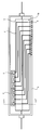
図1に示すように、DP-QPSK光変調器では、2つのマッハツェンダー型光導波路で構成されるネスト型光導波路を2つ配置した光導波路(不図示)をLN等の基板(光導波路基板)1に形成している。さらに、各マッハツェンダー型光導波路が構成する変調部に、変調信号を印加するため、基板1上には複数の信号電極2を備えている。各信号電極2には、入力用コネクタ4を介して変調信号が入力される。また、信号電極2の終端には、終端抵抗5が接続されている。各信号電極に対応して終端抵抗5が設けられる場合は、図1のように、複数の終端抵抗5を同一の終端基板3上に設け、光変調器の小型化を図る場合がある。LN等の基板(光導波路基板)1及び終端基板3は、筐体6内に配置され、パッケージ化される。
光変調器は高速で動作させるため、入力される電気信号が信号電極を伝搬して行く進行波型の電極構成が用いられる。信号電極に入力する信号周波数は、マイクロ波帯の高周波信号であり、これら入力された電気エネルギーは殆ど全て終端抵抗5で消費され、ここで熱に変換される。
DP-QPSK光変調器では、4つの変調部を持っている。本構成にて位相変調方式に対応するためには、従来の単一変調器構造の強度変調方式の2倍の電圧振幅(電力は4倍)で駆動される。このため、変調器内で消費される電力は、従来の単一変調器構造の変調器と比較して16倍以上になっている。しかも、光変調器の小型化要求に対応するために、終端基板3を光導波路基板1に近接して配置する必要があり、終端基板で発生する熱が大きな問題となっている。
しかも、図2に示すように、このDP-QPSK光変調器構成を2個以上に同一筐体に組み込んで、伝送容量の増大化を図る多素子化の場合、この発熱量は従来の単一変調器構造の強度変調方式の32倍以上の熱が発生することとなる。終端基板で発生した熱は、光変調器の温度ドリフトを劣化させる。また、終端抵抗自身の発熱は、終端抵抗の経時劣化、または、割れ・剥離等を発生させる要因となり、光変調器及びそれを用いた光送信装置の信頼性を損なうなど、深刻な問題となっている。なお、図2では、光導波路基板1a及び1bを横に並べて配置しているが、特許文献1のように複数の光導波路基板を積層して配置する場合もある。
これら終端基板での発熱の影響は、進行波型の電極構成を取る殆どの光変調器に内在するが、従来はこの問題について殆ど検討、対策がなされていなかった。むしろ、この発熱の影響は、光変調器が置かれる環境の温度変化又は、光変調器の不安定性の中に紛れ込み、本来の光変調器が持つ温度ドリフト等の特性劣化の問題として扱われていた。
しかしながら、これら影響は、DP-QPSK構成の光変調器などのように、(a)入力電気信号の振幅が大きいもの、(b)終端抵抗が複数有るもの、(c)終端抵抗が同一基板に有るものにおいては、特に影響が大きくなり、問題が深刻化してきた。しかも、光変調器が、(d)小型化すること、(e)複数素子化(多素子化)することにより、その影響が更に深刻化してきている。
この様な終端抵抗による発熱の問題を低減する対策として、特許文献2に示すように、終端抵抗の面積を大きくしたり、熱伝導孔を終端基板に設けたりすることが提案されている。しかしながら、これら構成、方法では終端基板自体が、大きくなり、また製造コストも増加するので、適応できる用途に制限が生じる。このため、様々な伝送フォーマットに適応でき、小型化又は低コスト化の要請に合致した解決策が望まれている。また、発熱対策を施した光変調器を搭載することで、温度ドリフトが抑圧され、信頼性の高い光送信装置が求められている。
本発明が解決しようとする課題は、上述したように、終端抵抗による発熱の影響を抑制した光変調器及びそれを用いた光送信装置を提供することである。特に、DP-QPSK光変調器のように、複数の信号入力、複数の終端抵抗を有する光変調器において、より顕著となる、終端抵抗の発熱を抑制することである。さらには、効果的な発熱対策を施すことにより、小型化、多素子化、そして、低コスト化にも対応した光変調器及びそれを用いた光送信装置を提供することである。
上記課題を解決するため、本発明の光変調器及びそれを用いた光送信装置は、以下のような技術的特徴を有する。
(1) 光導波路が形成された光導波路基板と、該光導波路基板に設けられ、該光導波路に電界を印加する信号電極と、該信号電極を終端する終端抵抗が設けられた終端基板と、該光導波路基板と該終端基板とを搭載する筐体とを備えた光変調器において、該終端抵抗で発生した熱が、該筐体を介して該光導波路基板に伝導するのを抑制するため、該終端基板と該光導波路基板との間に、該筐体に溝が形成されていることを特徴とする。
(1) 光導波路が形成された光導波路基板と、該光導波路基板に設けられ、該光導波路に電界を印加する信号電極と、該信号電極を終端する終端抵抗が設けられた終端基板と、該光導波路基板と該終端基板とを搭載する筐体とを備えた光変調器において、該終端抵抗で発生した熱が、該筐体を介して該光導波路基板に伝導するのを抑制するため、該終端基板と該光導波路基板との間に、該筐体に溝が形成されていることを特徴とする。
(2) 光導波路が形成された光導波路基板と、該光導波路基板に設けられ、該光導波路に電界を印加する信号電極と、該信号電極を終端する終端抵抗が設けられた終端基板と、該光導波路基板と該終端基板とを搭載する筐体とを備えた光変調器において、該終端抵抗で発生した熱が、該筐体を介して該光導波路基板に伝導するのを抑制するため、該終端基板が配置される筐体の一部に、良熱伝導性材料を設けたことを特徴とする。
(3) 上記(2)に記載の光変調器において、該良熱伝導体材料は、Cu-W、Cu-Mo、Al-SiCの各複合体のうち、少なくとも1種類を用いることを特徴とする。
(4) 光導波路が形成された光導波路基板と、該光導波路基板に設けられ、該光導波路に電界を印加する信号電極と、該信号電極を終端する終端抵抗が設けられた終端基板と、該光導波路基板と該終端基板とを搭載する筐体とを備えた光変調器において、該終端抵抗で発生した熱が、該筐体を介して該光導波路基板に伝導するのを抑制するため、該終端基板を薄片化したことを特徴とする。
(5) 光導波路が形成された光導波路基板と、該光導波路基板に設けられ、該光導波路に電界を印加する信号電極と、該信号電極を終端する終端抵抗が設けられた終端基板と、該光導波路基板と該終端基板とを搭載する筐体とを備えた光変調器において、該終端抵抗で発生した熱が、該筐体を介して該光導波路基板に伝導するのを抑制するため、該終端基板が搭載される筐体の搭載面と、該光導波路基板が搭載される筐体の搭載面との間に段差を設けたことを特徴とする。
(6) 上記(5)に記載の光変調器において、該終端基板が薄片化され、かつ、前記終端基板が搭載される筐体の搭載面が、前記光導波路基板が搭載される筐体の搭載面より高い位置に設けられていることを特徴とする。
(7) 上記(5)に記載の光変調器において、前記終端基板が搭載される筐体の搭載面が、前記光導波路基板が搭載される筐体の搭載面より低い位置に設けられていることを特徴とする。
(8) 光導波路が形成された光導波路基板と、該光導波路基板に設けられ、該光導波路に電界を印加する信号電極と、該信号電極を終端する終端抵抗が設けられた終端基板と、該光導波路基板と該終端基板とを搭載する筐体とを備えた光変調器において、該終端抵抗で発生した熱が、該筐体を介して該光導波路基板に伝導するのを抑制するため、該終端基板と該筐体との間に、良熱伝導部材を設置したことを特徴とする。
(9) 上記(8)に記載の光変調器において、該終端基板を薄片化したことを特徴とする。
(10) 光導波路が形成された光導波路基板と、該光導波路基板に設けられ、該光導波路に電界を印加する信号電極と、該信号電極を終端する終端抵抗が設けられた終端基板と、該光導波路基板と該終端基板とを搭載する筐体とを備えた光変調器において、該終端抵抗で発生した熱が、該筐体を介して該光導波路基板に伝導するのを抑制するため、該終端基板が搭載される筐体の搭載面と、該光導波路基板が搭載される筐体の搭載面との間に段差を設け、かつ該終端基板の一部を該段差の角部から突き出すように配置することを特徴とする。
(11) 光導波路が形成された光導波路基板と、該光導波路基板に設けられ、該光導波路に電界を印加する信号電極と、該信号電極を終端する終端抵抗が設けられた終端基板と、該光導波路基板と該終端基板とを搭載する筐体とを備えた光変調器において、該終端抵抗で発生した熱が、該筐体を介して該光導波路基板に伝導するのを抑制するため、該終端基板が搭載される筐体の搭載面と、該光導波路基板が搭載される筐体の搭載面との間に段差を設け、かつ該段差の近傍の筐体に溝を形成したことを特徴とする。
(12) 上記(11)に記載の光変調器において、該終端基板の一部を該段差の角部から突き出すように配置することを特徴とする。
(13) 光導波路が形成された光導波路基板と、該光導波路基板に設けられ、該光導波路に電界を印加する信号電極と、該信号電極を終端する終端抵抗が設けられた終端基板と、該光導波路基板と該終端基板とを搭載する筐体とを備えた光変調器において、該終端抵抗で発生した熱が、該筐体を介して該光導波路基板に伝導するのを抑制するため、該終端基板が搭載される筐体の搭載面と、該光導波路基板が搭載される筐体の搭載面との間に段差を設け、かつ該終端基板の端部で該段差の角部に最も近い端部が、該段差の角部より引っ込んで配置されていることを特徴とする。
(14) 上記(1)乃至(13)のいずれかに記載の光変調器において、該終端基板の底面又は側面の少なくとも一部が、Agフィラーを含有する熱伝導性接着剤で、該筐体に固定されていることを特徴とする。
(15) 上記(1)乃至(14)のいずれかに記載の光変調器において、該終端基板には、少なくとも2個以上の終端抵抗が設けられていることを特徴とする。
(16) 上記(1)乃至(15)のいずれかに記載の光変調器において、該光導波路基板は、LiNbO3、InP、GaAs、Siの中から選定された材料で構成されていることを特徴とする。
(17) 上記(1)乃至(16)のいずれかに記載の光変調器と、該光変調器に印加するデータ信号を発生するデータ発生部と、該光変調器に光波を入力する光源とを備えることを特徴とする光送信装置である。
本発明により、終端抵抗で発生する熱を効果的に筐体側に放出することができ、しかも、筐体に放出された熱が、筐体を固定する光送信装置側へ伝導することにより筐体を介して光導波路基板に伝導することを抑制できるため、光導波路基板に対する熱の影響を低減することが可能となる。これにより、温度ドリフトが抑圧され信頼性の高い、小型で低コストな光変調器を提供することができる。そして、本発明の光変調器を搭載することにより、高信頼で温度ドリフトが抑圧された光送信装置を提供することも可能となる。
以下、本発明の一態様に係る光変調器について、図3乃至14を用いて詳細に説明する。
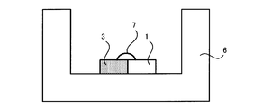
図3は、図1又は図2のX-X’における断面図であり、光導波路基板1と終端抵抗基板3の実装状態を示した従来構成例の断面図である。光導波路基板1は、LiNbO3又はLiTaO3等の誘電体、InP又はSi等の半導体を用いたものなどがある。本発明の光変調器においても、光導波路基板の材料は特に限定されないが、従来から公知の誘電体又は半導体の基板を用いることできる。また、光導波路の形成に際しても、LiNbO3の誘電体基板にTiを熱拡散させ光導波路を形成する方法、リッジ型光導波路など、公知の技術を用いることが可能である。
図3は、図1又は図2のX-X’における断面図であり、光導波路基板1と終端抵抗基板3の実装状態を示した従来構成例の断面図である。光導波路基板1は、LiNbO3又はLiTaO3等の誘電体、InP又はSi等の半導体を用いたものなどがある。本発明の光変調器においても、光導波路基板の材料は特に限定されないが、従来から公知の誘電体又は半導体の基板を用いることできる。また、光導波路の形成に際しても、LiNbO3の誘電体基板にTiを熱拡散させ光導波路を形成する方法、リッジ型光導波路など、公知の技術を用いることが可能である。
光導波路の構成は、1つのマハツェンダー型光導波路、2つのマッハツェンダー型光導波路を入れ子型に配置した、所謂、ネスト型光導波路、さらに、特許文献1にも開示されているDP-QPSK光変調器などのように、2つのマッハツェンダー型光導波路で構成されるネスト型光導波路を2つ配置したものなど、種々の光導波路の形状を用いることができる。
また、光導波路の変調部に入力電気信号を印加する信号電極の数についても、図1に示すように、4つの信号電極を備えたDP-QPSK光変調器に限らず、シングル型(変調用の信号電極が1箇所)、デュアル型(変調用の信号電極が2箇所)、DQPSK構成変調器(変調用の信号電極が2箇所)など、種々のものに本発明は適用可能である。特に、信号電極の数が多い程、本発明は効果的に適用可能であり、例えば、図2に示すように、DP-QPSK光変調器を2個組み込み、入力電気信号が8箇所ある多素子化した構成には、特に効果的に適用できる。
図3の従来例でも示すように、終端基板3は入力される高周波信号の反射及び透過特性を劣化させないよう、出来るだけ光導波路基板1に近づけた状態で、段差なく上面高さを略一致させるよう配置してもよい。このため、従来では、図3に示すように、筐体6の終端基板3、光導波路基板1の実装面は、基板及び素子の実装容易性又は筐体加工容易性の観点から、特段の要請が無い限りフラットな構成が採用されていた。また、終端基板3の配線と光導波路基板の配線との接続は、通常、符号7で示すような、Auボンディング等で結線し、入力電気信号が出来るだけ効率よく終端基板3に伝搬するよう構成されている。
終端基板3上に形成される終端抵抗の素子数は、光変調器の構成、電極設計、筐体設計に応じて適宜選択される。図1のDP-QPSK構成の光変調器では4個の終端抵抗を同一終端基板上に形成した例を示しているが、終端基板を複数で構成することも可能である。さらに、図1の4個の終端抵抗を2個又は1個の終端抵抗を備えた終端用電気回路で構成し、これらを同じ基板上に形成しても良い。近年では、光変調器サイズを小型化するため、複数の終端抵抗を同一基板上に形成する場合が多い。本発明は、図1又は図2のように、2個以上の終端抵抗を用いるもの、特に、複数の終端抵抗を同一の終端基板上に配置する場合に、効果的に適用することが可能である。
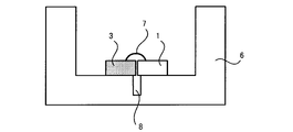
図4は、本発明の光変調器の第1実施例を示す断面図である。図3と同様に、図1又は図2のX-X’における断面図に相当する。
本実施例では、終端基板3と光導波路基板1の間の筐体6に溝8を入れ、終端基板の発熱が筐体を伝導し、光導波路基板に影響することを抑圧する構成となっている。
本実施例では、終端基板3と光導波路基板1の間の筐体6に溝8を入れ、終端基板の発熱が筐体を伝導し、光導波路基板に影響することを抑圧する構成となっている。
通常、筐体は、切削加工性又はレーザー溶接、封止などの組み立て工程を考慮し、SUS又はコバール等の金属材料から選ばれる。これら金属材料は終端基板等に比べ熱伝導性が良く、終端抵抗での発熱が金属筐体6を介して、光導波路基板に伝導する。この影響を低減、抑圧させるために筐体の一部に溝8を形成している。
溝の幅(図4の溝8の左右方向の幅)は広いほど終端発熱の影響を抑圧できるが、小型であっても筐体剛性を高め、光導波路基板及び終端基板の実装に影響を与えないようにするため、0.1mmから1mm程度の幅に設定してもよい。また、溝の深さは、深いほど終端抵抗における発熱の影響を抑圧することができるが、筐体厚さの制限から、0.5mmから2mm程度の範囲に設定してもよい。
図5は、本発明の光変調器の第2実施例を示す図である。
本実施例では、筐体6の終端基板3の実装面に良熱伝導材9を入れるものである。良熱伝導材は筐体材料より高い熱伝導性を持つ材料のことを意味しており、より具体的にはSUS又はコバールより熱伝導性の高い、Cu-W、Cu-Mo、Al-SiC複合体等が選ばれる。
本実施例では、筐体6の終端基板3の実装面に良熱伝導材9を入れるものである。良熱伝導材は筐体材料より高い熱伝導性を持つ材料のことを意味しており、より具体的にはSUS又はコバールより熱伝導性の高い、Cu-W、Cu-Mo、Al-SiC複合体等が選ばれる。
この良熱伝導材9は終端基板での発熱を、より効果的に、より選択的に、筐体外へ放出するよう、終端基板3の下に設置し、筐体外部まで達するよう形成してもよい。このような構成は、先ず筐体の一部にくりぬき部を形成し、その後そのくりぬき部と略同形状の良熱伝導材を銀ロウ又は金スズ等で固定し形成する。なお、筐体内の気密性を高めるため、筐体を完全にくり貫かずに、内側底面等に凹部を設ける構成とし、該凹部に良熱伝導材を配置することも可能である。
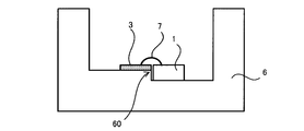
図6は、本発明の光変調器の第3実施例を示す図である。
本発明では、終端基板3の厚さを薄く(薄片化)する実施例である。終端基板に用いられる材料は、マイクロ波帯等の高周波で使用されることから高周波特性に優れたアルミナ等のセラミック材料などがよく使われる。これらセラミック材料は一般的に金属材料と比べ熱伝導性に劣るので、終端基板で発生した熱を効率的に基板外へ移すため、終端基板を薄片化することが効果的である。
本発明では、終端基板3の厚さを薄く(薄片化)する実施例である。終端基板に用いられる材料は、マイクロ波帯等の高周波で使用されることから高周波特性に優れたアルミナ等のセラミック材料などがよく使われる。これらセラミック材料は一般的に金属材料と比べ熱伝導性に劣るので、終端基板で発生した熱を効率的に基板外へ移すため、終端基板を薄片化することが効果的である。
薄片化された終端基板3の厚さは、終端基板に用いる材料の強度、熱伝導性、および、大きさなど、総合的に考慮し選定する必要があるが、少なくとも光導波路が形成され、終端基板の横に設置するチップの厚さ(通常0.5mm~2.0mm)より薄くしてもよい。終端抵抗で発生する熱の放熱を考えると薄ければ薄いほど有利であるが、機械的強度又は終端抵抗のインピーダンス設計を考慮すると、0.05mmから0.8mmの範囲に設定することが好適である。
終端抵抗により発生した熱は、終端基板が薄く形成されているので、効率的に筐体側へ伝導される。これにより、終端抵抗自身が高熱になることが抑制され、終端抵抗の経時劣化又は割れ・剥離等の信頼性問題を解決することができる。また、終端基板が実装される筐体の厚みを、図6に示すように、光導波路基板が実装される部分より厚くするため、筐体の厚い部分の方向に熱が拡散し易くなり、光変調器の温度ドリフトも有効に低減することができる。
本実施例のように、終端基板と光導波路基板の搭載面に段差60を設けることは、熱伝導の非対称性を生み、この段差構成だけでも、終端抵抗の発熱が光導波路基板に伝導する影響を低減させる作用を持つ。
図7は、本発明の光変調器の第4実施例を示す図である。
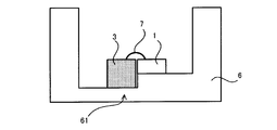
本発明では、終端基板3を実装する筐体6の底面(符号61参照)の肉厚を薄くする実施例である。この実施例では、終端基板の発熱を筐体外に効率的に放出するため、発熱する終端基板の下側に位置する筐体61の肉厚を薄くし、筐体6を固定する光送信装置の構造体へ、熱を効率的に放出するような構成にしている。
本発明では、終端基板3を実装する筐体6の底面(符号61参照)の肉厚を薄くする実施例である。この実施例では、終端基板の発熱を筐体外に効率的に放出するため、発熱する終端基板の下側に位置する筐体61の肉厚を薄くし、筐体6を固定する光送信装置の構造体へ、熱を効率的に放出するような構成にしている。
この部分の肉厚は薄いほど効率的に熱を外部に放出することが出来るようになるが、筐体剛性を一定レベルで維持すること、及び筐体の厚さの制限等から、0.2mm~2mm程度の範囲に設定してもよい。この場合も、終端基板3と光導波路基板1との搭載面に段差を形成される。2つの基板の上面の高さを一致させるので、図7のように、終端基板の厚さを厚くしても良いし、または、終端基板の厚さは変えず、光導波路基板の厚さを薄くしても良い。
図8は、本発明の光変調器の第5実施例を示す図である。
本実施例では、図7の構成に加え、終端基板3の下に良熱伝導材10を設けることを特徴としている。本構成では終端基板での発熱を、良導電材料を用いて、効率的に終端基板から筐体へ熱伝導を促進させる構成を採用している。図8の実施例では、終端基板の厚みは変えず、筐体の肉厚を薄くした分の厚さで良熱伝導体を入れた構成例を示しているが、終端基板をさらに薄片化し、良熱伝導体を入れる構成は、より好適な実施例となる。良熱伝導体の材料又は薄片の厚さなどは、上述したとおりである。
本実施例では、図7の構成に加え、終端基板3の下に良熱伝導材10を設けることを特徴としている。本構成では終端基板での発熱を、良導電材料を用いて、効率的に終端基板から筐体へ熱伝導を促進させる構成を採用している。図8の実施例では、終端基板の厚みは変えず、筐体の肉厚を薄くした分の厚さで良熱伝導体を入れた構成例を示しているが、終端基板をさらに薄片化し、良熱伝導体を入れる構成は、より好適な実施例となる。良熱伝導体の材料又は薄片の厚さなどは、上述したとおりである。
図9は、本発明の光変調器の第6実施例を示す図である。
本実施例の構成は、図8で示した終端基板と光導波路基板との搭載面に段差を設ける構成に対し、従来例と同様に筐体に段差を設けない構成となっている。この構成では、発熱の影響を、終端基板3の薄片化と良熱伝導材10の設置により、ある程度抑圧しつつ、終端基板及び光導波路基板の実装容易性と筐体製造容易性を兼ね備えることも、併せて実現することが可能である。
本実施例の構成は、図8で示した終端基板と光導波路基板との搭載面に段差を設ける構成に対し、従来例と同様に筐体に段差を設けない構成となっている。この構成では、発熱の影響を、終端基板3の薄片化と良熱伝導材10の設置により、ある程度抑圧しつつ、終端基板及び光導波路基板の実装容易性と筐体製造容易性を兼ね備えることも、併せて実現することが可能である。
図10は、本発明の光変調器の第7実施例を示す図である。
本発明の実施例では、終端基板3を薄片化し、搭載面63から終端基板3の一部30を突き出すよう構成している。この構成では、発熱する終端基板3から熱が効率的に金属筐体6へ伝導し、かつ終端基板の一部を突き出した構成により、終端基板と光導波路基板との間に、筐体の段差と終端基板3の突き出し量に応じた空間が形成されるので、筐体を介した熱伝導の影響が更に抑制される。
本発明の実施例では、終端基板3を薄片化し、搭載面63から終端基板3の一部30を突き出すよう構成している。この構成では、発熱する終端基板3から熱が効率的に金属筐体6へ伝導し、かつ終端基板の一部を突き出した構成により、終端基板と光導波路基板との間に、筐体の段差と終端基板3の突き出し量に応じた空間が形成されるので、筐体を介した熱伝導の影響が更に抑制される。
この突き出し量は、大きいほど熱影響の抑圧効果が高く、現実的には終端基板の実装性又はAuボンディングに対する影響を考慮する必要があるものの、選択の幅は広く、およそ10μmから2mm程度の範囲内で設定される。このように終端基板3の一部を突き出した構成であっても、終端基板3の上面と光導波路基板1の上面が略同一高さであり、さらに、両者の間隔が狭い場合には、高周波特性を犠牲にすることも避けることが可能である。この場合の両者の間隔は、100μm以下に設定してもよい。
図11は、本発明の光変調器の第8実施例を示す図である。
本発明の構成は、図10の構成に加え、更に筐体に溝8を入れ、終端抵抗により発生した熱の影響が、光導波路基板へ及ぶことを抑制するものである。終端基板の厚さ、突き出し量、溝の幅又は深さ等は、上述した内容と同等であるので、ここでの説明は省略する。この図11の構成は、列挙する幾つかの実施例の中では、熱影響の抑制に最も効果が高いものである。
本発明の構成は、図10の構成に加え、更に筐体に溝8を入れ、終端抵抗により発生した熱の影響が、光導波路基板へ及ぶことを抑制するものである。終端基板の厚さ、突き出し量、溝の幅又は深さ等は、上述した内容と同等であるので、ここでの説明は省略する。この図11の構成は、列挙する幾つかの実施例の中では、熱影響の抑制に最も効果が高いものである。
図12は、本発明の光変調器の第9実施例を示す図である。
本実施例では、薄片化した終端基板3の端部31を、段差を付けた筐体実装面の角部64から引っ込んで配置することを特徴としている。この構成では、終端基板3での発熱が、終端基板の下側に位置する筐体部分へ多く伝導し、光導波路基板が搭載された部分には伝導が少なくなる。しかも、終端基板3と光導波路基板1との間隔が広くなるので、熱影響をより低減できる構成となっている。
本実施例では、薄片化した終端基板3の端部31を、段差を付けた筐体実装面の角部64から引っ込んで配置することを特徴としている。この構成では、終端基板3での発熱が、終端基板の下側に位置する筐体部分へ多く伝導し、光導波路基板が搭載された部分には伝導が少なくなる。しかも、終端基板3と光導波路基板1との間隔が広くなるので、熱影響をより低減できる構成となっている。
また、本構成により、終端基板3の実装トレランスを拡大し、組立工数削減又は光導波路基板1との干渉による弊害(割れ、欠けなど)も抑制する効果がある。筐体の段差の角部64から終端基板の端部31を引っ込めた距離は、大きいほど熱影響を低減する効果は高いが、高周波信号の反射又は伝送特性に対する悪影響を考慮すると、100μm程度の範囲内に設定してもよい。
図13は、本発明の光変調器の第10実施例を示す図である。
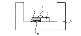
本実施例では、発熱する終端基板3の底面又は側面をAgフィラーを含有する熱伝導性接着剤11で固定したことを特徴としている。Agフィラーを含有する熱伝導性接着剤は、通常の接着剤に比べ粘性調整及び硬化作業がし易く、終端基板3を精度高く、作業性良く、筐体6に実装できると同時に、電気伝導性も高いので高周波特性を安定化させることもできる。また、終端基板の底面と側面との両方に、Agフィラーを含有する熱伝導性接着剤を使用することにより、終端基板の発熱をより効率的に熱伝導させることが可能となる。さらに、Agフィラーを含有する接着剤は、特に、終端基板の側面から熱を効率良く筐体で伝導させるために、終端基板側面に対し、厚く高く形成することが容易になるなど、様々な利点も備えている。
本実施例では、発熱する終端基板3の底面又は側面をAgフィラーを含有する熱伝導性接着剤11で固定したことを特徴としている。Agフィラーを含有する熱伝導性接着剤は、通常の接着剤に比べ粘性調整及び硬化作業がし易く、終端基板3を精度高く、作業性良く、筐体6に実装できると同時に、電気伝導性も高いので高周波特性を安定化させることもできる。また、終端基板の底面と側面との両方に、Agフィラーを含有する熱伝導性接着剤を使用することにより、終端基板の発熱をより効率的に熱伝導させることが可能となる。さらに、Agフィラーを含有する接着剤は、特に、終端基板の側面から熱を効率良く筐体で伝導させるために、終端基板側面に対し、厚く高く形成することが容易になるなど、様々な利点も備えている。
以上のような本発明の構成を採用することにより、終端基板の実装作業性が格段に向上すると同時に、高周波特性に優れ、終端発熱を効果的に低減した光変調器を提供することができる。
図14は、本発明の光変調器を搭載した光送信装置の構成例である。
光送信装置の基本構成は、光変調器に導入する光波を発生する光源、光変調器、光変調器に信号を印加するデータ生成部、及び光変調器から発生する変調光を外部に導出するための光ファイバから構成される。
光送信装置の基本構成は、光変調器に導入する光波を発生する光源、光変調器、光変調器に信号を印加するデータ生成部、及び光変調器から発生する変調光を外部に導出するための光ファイバから構成される。
光送信装置は、稼働を開始させると光変調器が温度ドリフトする。伝送特性を高品質で安定化させるため、光変調器の動作点を適切な状態を保つよう制御しながら運用することは必要となる。この温度ドリフトは、従来、光源又はデータ生成部など光変調器周辺機器の発熱の影響、と考えられていた。
しかしながら、DP-QPSK光変調器又は小型光変調器などにおいては、光送信装置の稼働開始直後に大きな温度ドリフトが発生し、光伝送装置の伝送特性が非常に不安定になる場合が発生している。この原因について、本発明者が鋭意検討を重ねた結果、従来考えられていたような、周辺機器の発熱、環境温度変化では説明できないことが判明した。そして、光変調器自身の内部にある終端抵抗の発熱が影響することを見出し、特に、高周波信号を複数入力する光変調器構成において、複数の終端抵抗を同一基板に形成する場合、入力信号の振幅が大きい場合、さらには光変調器を小型にした場合等に、特に顕著に発生する現象であることを見出した。
この問題に対し、本発明を施した光変調器を光送信装置に配置することにより、終端抵抗の発熱による温度ドリフトを低減することができ、伝送特性を高品で安定化させることができる。
上述した実施例は、LiNbO3基板を用いたDP-QPSK光変調器の構成に限らず、終端抵抗を有する光変調器であり、終端抵抗の発熱が光変調器の特性に影響を及ぼすものであれば、変調方式に依らず本発明を適用できる。また、光導波路基板は、InP又はSi等半導体系材料のものでも良いし、LiNbO3基板を用いた場でも、Xcut又はZcutなど結晶方位に依らず、本発明が適用できることは言うまでもない。
また、上述した実施例では、終端抵抗だけが基板上に形成された終端基板の例を示したが、コンデンサ又はその他の電子部品、貫通導体又は多層化含めた電子回路が同じ終端基板上に形成されていても良い。また、終端抵抗が別々の終端基板に形成されていても良いことは言うまでもない。
以上、説明したように、本発明によれば、温度ドリフトが抑圧され信頼性の高い、小型で低コストな光変調器を提供することができる。また本発明の光変調器を搭載した、高信頼で温度ドリフトが抑圧された光送信装置を提供することができる。
1 光導波路基板
2 信号電極
3 終端基板
4 信号入力用コネクタ
5 終端抵抗(発熱部)
6 筐体
7 電気接続ワイヤ(Auボンディング)
8 筐体部溝
9 筐体段差
10 良熱伝導材
11 熱伝導性接着剤
2 信号電極
3 終端基板
4 信号入力用コネクタ
5 終端抵抗(発熱部)
6 筐体
7 電気接続ワイヤ(Auボンディング)
8 筐体部溝
9 筐体段差
10 良熱伝導材
11 熱伝導性接着剤
Claims (17)
- 光導波路が形成された光導波路基板と、
該光導波路基板に設けられ、該光導波路に電界を印加する信号電極と、
該信号電極を終端する終端抵抗が設けられた終端基板と、
該光導波路基板と該終端基板とを搭載する筐体とを備えた光変調器において、
該終端抵抗で発生した熱が、該筐体を介して該光導波路基板に伝導するのを抑制するため、
該終端基板と該光導波路基板との間に、該筐体に溝が形成されていることを特徴とする光変調器。 - 光導波路が形成された光導波路基板と、
該光導波路基板に設けられ、該光導波路に電界を印加する信号電極と、
該信号電極を終端する終端抵抗が設けられた終端基板と、
該光導波路基板と該終端基板とを搭載する筐体とを備えた光変調器において、
該終端抵抗で発生した熱が、該筐体を介して該光導波路基板に伝導するのを抑制するため、
該終端基板が配置される筐体の一部に、良熱伝導性材料を設けたことを特徴とする光変調器。 - 請求項2に記載の光変調器において、該良熱伝導体材料は、Cu-W、Cu-Mo、Al-SiCの各複合体のうち、少なくとも1種類を用いることを特徴とする光変調器。
- 光導波路が形成された光導波路基板と、
該光導波路基板に設けられ、該光導波路に電界を印加する信号電極と、
該信号電極を終端する終端抵抗が設けられた終端基板と、
該光導波路基板と該終端基板とを搭載する筐体とを備えた光変調器において、
該終端抵抗で発生した熱が、該筐体を介して該光導波路基板に伝導するのを抑制するため、
該終端基板を薄片化したことを特徴とする光変調器。 - 光導波路が形成された光導波路基板と、
該光導波路基板に設けられ、該光導波路に電界を印加する信号電極と、
該信号電極を終端する終端抵抗が設けられた終端基板と、
該光導波路基板と該終端基板とを搭載する筐体とを備えた光変調器において、
該終端抵抗で発生した熱が、該筐体を介して該光導波路基板に伝導するのを抑制するため、
該終端基板が搭載される筐体の搭載面と、該光導波路基板が搭載される筐体の搭載面との間に段差を設けたことを特徴とする光変調器。 - 請求項5に記載の光変調器において、該終端基板が薄片化され、かつ、前記終端基板が搭載される筐体の搭載面が、前記光導波路基板が搭載される筐体の搭載面より高い位置に設けられていることを特徴とする光変調器。
- 請求項5に記載の光変調器において、前記終端基板が搭載される筐体の搭載面が、前記光導波路基板が搭載される筐体の搭載面より低い位置に設けられていることを特徴とする光変調器。
- 光導波路が形成された光導波路基板と、
該光導波路基板に設けられ、該光導波路に電界を印加する信号電極と、
該信号電極を終端する終端抵抗が設けられた終端基板と、
該光導波路基板と該終端基板とを搭載する筐体とを備えた光変調器において、
該終端抵抗で発生した熱が、該筐体を介して該光導波路基板に伝導するのを抑制するため、
該終端基板と該筐体との間に、良熱伝導部材を設置したことを特徴とする光変調器。 - 請求項8に記載の光変調器において、該終端基板を薄片化したことを特徴とする光変調器。
- 光導波路が形成された光導波路基板と、
該光導波路基板に設けられ、該光導波路に電界を印加する信号電極と、
該信号電極を終端する終端抵抗が設けられた終端基板と、
該光導波路基板と該終端基板とを搭載する筐体とを備えた光変調器において、
該終端抵抗で発生した熱が、該筐体を介して該光導波路基板に伝導するのを抑制するため、
該終端基板が搭載される筐体の搭載面と、該光導波路基板が搭載される筐体の搭載面との間に段差を設け、かつ該終端基板の一部を該段差の角部から突き出すように配置することを特徴とする光変調器。 - 光導波路が形成された光導波路基板と、
該光導波路基板に設けられ、該光導波路に電界を印加する信号電極と、
該信号電極を終端する終端抵抗が設けられた終端基板と、
該光導波路基板と該終端基板とを搭載する筐体とを備えた光変調器において、
該終端抵抗で発生した熱が、該筐体を介して該光導波路基板に伝導するのを抑制するため、
該終端基板が搭載される筐体の搭載面と、該光導波路基板が搭載される筐体の搭載面との間に段差を設け、かつ該段差の近傍の筐体に溝を形成したことを特徴とする光変調器。 - 請求項11に記載の光変調器において、該終端基板の一部を該段差の角部から突き出すように配置することを特徴とする光変調器。
- 光導波路が形成された光導波路基板と、
該光導波路基板に設けられ、該光導波路に電界を印加する信号電極と、
該信号電極を終端する終端抵抗が設けられた終端基板と、
該光導波路基板と該終端基板とを搭載する筐体とを備えた光変調器において、
該終端抵抗で発生した熱が、該筐体を介して該光導波路基板に伝導するのを抑制するため、
該終端基板が搭載される筐体の搭載面と、該光導波路基板が搭載される筐体の搭載面との間に段差を設け、かつ該終端基板の端部で該段差の角部に最も近い端部が、該段差の角部より引っ込んで配置されていることを特徴とする光変調器。 - 請求項1乃至13のいずれかに記載の光変調器において、該終端基板の底面又は側面の少なくとも一部が、Agフィラーを含有する熱伝導性接着剤で、該筐体に固定されていることを特徴とする光変調器。
- 請求項1乃至14のいずれかに記載の光変調器において、該終端基板には、少なくとも2個以上の終端抵抗が設けられていることを特徴とする光変調器。
- 請求項1乃至15のいずれかに記載の光変調器において、該光導波路基板は、LiNbO3、InP、GaAs、Siの中から選定された材料で構成されていることを特徴とする光変調器。
- 請求項1乃至16のいずれかに記載の光変調器と、
該光変調器に印加するデータ信号を発生するデータ発生部と、
該光変調器に光波を入力する光源とを備えることを特徴とする光送信装置。
Priority Applications (3)
| Application Number | Priority Date | Filing Date | Title |
|---|---|---|---|
| US16/073,965 US10732481B2 (en) | 2016-01-28 | 2016-08-30 | Optical modulator and optical transmission device using same |
| CN201680078654.3A CN108474971B (zh) | 2016-01-28 | 2016-08-30 | 光调制器及使用该光调制器的光发送装置 |
| US16/911,573 US11187959B2 (en) | 2016-01-28 | 2020-06-25 | Optical modulator and optical transmission device using same |
Applications Claiming Priority (2)
| Application Number | Priority Date | Filing Date | Title |
|---|---|---|---|
| JP2016014087A JP6183479B2 (ja) | 2016-01-28 | 2016-01-28 | 光変調器及びそれを用いた光送信装置 |
| JP2016-014087 | 2016-01-28 |
Related Child Applications (2)
| Application Number | Title | Priority Date | Filing Date |
|---|---|---|---|
| US16/073,965 A-371-Of-International US10732481B2 (en) | 2016-01-28 | 2016-08-30 | Optical modulator and optical transmission device using same |
| US16/911,573 Division US11187959B2 (en) | 2016-01-28 | 2020-06-25 | Optical modulator and optical transmission device using same |
Publications (1)
| Publication Number | Publication Date |
|---|---|
| WO2017130450A1 true WO2017130450A1 (ja) | 2017-08-03 |
Family
ID=59397595
Family Applications (1)
| Application Number | Title | Priority Date | Filing Date |
|---|---|---|---|
| PCT/JP2016/075313 Ceased WO2017130450A1 (ja) | 2016-01-28 | 2016-08-30 | 光変調器及びそれを用いた光送信装置 |
Country Status (4)
| Country | Link |
|---|---|
| US (2) | US10732481B2 (ja) |
| JP (1) | JP6183479B2 (ja) |
| CN (2) | CN112965168A (ja) |
| WO (1) | WO2017130450A1 (ja) |
Cited By (1)
| Publication number | Priority date | Publication date | Assignee | Title |
|---|---|---|---|---|
| WO2020115999A1 (ja) * | 2018-12-05 | 2020-06-11 | 住友大阪セメント株式会社 | 光変調器 |
Families Citing this family (5)
| Publication number | Priority date | Publication date | Assignee | Title |
|---|---|---|---|---|
| JP7087360B2 (ja) * | 2017-11-30 | 2022-06-21 | 住友大阪セメント株式会社 | 光変調器及びそれを用いた光送信装置 |
| JP7098930B2 (ja) * | 2017-12-28 | 2022-07-12 | 住友大阪セメント株式会社 | 光変調器及びそれを用いた光送信装置 |
| JP7135382B2 (ja) * | 2018-03-30 | 2022-09-13 | 住友大阪セメント株式会社 | 光変調器、及び光送信装置 |
| JP7135645B2 (ja) * | 2018-09-19 | 2022-09-13 | 住友大阪セメント株式会社 | 光モジュール |
| CN119024582B (zh) * | 2023-05-23 | 2025-10-17 | 济南量子技术研究院 | 一种铌酸锂调制器 |
Citations (4)
| Publication number | Priority date | Publication date | Assignee | Title |
|---|---|---|---|---|
| WO2003005091A2 (en) * | 2001-07-04 | 2003-01-16 | Alcatel Optronics Uk Limited | Packaged optoelectronic device |
| JP2005128440A (ja) * | 2003-10-27 | 2005-05-19 | Fujitsu Ltd | 電気回路を内蔵する光導波路モジュール及びその製造方法 |
| JP2007065247A (ja) * | 2005-08-31 | 2007-03-15 | Nippon Telegr & Teleph Corp <Ntt> | 光モジュール |
| JP2014199302A (ja) * | 2013-03-29 | 2014-10-23 | 住友大阪セメント株式会社 | 光デバイス |
Family Cites Families (11)
| Publication number | Priority date | Publication date | Assignee | Title |
|---|---|---|---|---|
| US5155778A (en) * | 1991-06-28 | 1992-10-13 | Texas Instruments Incorporated | Optical switch using spatial light modulators |
| JP2002131712A (ja) * | 2000-10-19 | 2002-05-09 | Mitsubishi Electric Corp | 光デバイスおよびその製造方法 |
| US20020154843A1 (en) * | 2001-04-19 | 2002-10-24 | Betts Gary E. | Dielectric backfill for optical modulators using ridged substrates |
| JP4792276B2 (ja) * | 2005-11-16 | 2011-10-12 | 住友大阪セメント株式会社 | 光変調器 |
| JP5092494B2 (ja) * | 2007-03-29 | 2012-12-05 | 住友大阪セメント株式会社 | 光導波路素子、及び光導波路素子の温度クロストーク抑止方法 |
| US7848599B2 (en) * | 2009-03-31 | 2010-12-07 | Oracle America, Inc. | Optical device with large thermal impedance |
| JP6268883B2 (ja) | 2013-09-30 | 2018-01-31 | 住友大阪セメント株式会社 | 光変調器 |
| US9513497B2 (en) * | 2014-02-05 | 2016-12-06 | Aurrion, Inc. | Opto-electronic modulator utilizing one or more heating elements |
| CN206627719U (zh) * | 2014-02-14 | 2017-11-10 | 古河电气工业株式会社 | 光模块 |
| JP6330548B2 (ja) * | 2014-07-23 | 2018-05-30 | 住友電気工業株式会社 | 変調器およびその製造方法 |
| JP5949857B2 (ja) * | 2014-08-29 | 2016-07-13 | 住友大阪セメント株式会社 | 光変調器、及び光スイッチ |
-
2016
- 2016-01-28 JP JP2016014087A patent/JP6183479B2/ja active Active
- 2016-08-30 CN CN202110249992.1A patent/CN112965168A/zh active Pending
- 2016-08-30 WO PCT/JP2016/075313 patent/WO2017130450A1/ja not_active Ceased
- 2016-08-30 US US16/073,965 patent/US10732481B2/en active Active
- 2016-08-30 CN CN201680078654.3A patent/CN108474971B/zh active Active
-
2020
- 2020-06-25 US US16/911,573 patent/US11187959B2/en active Active
Patent Citations (4)
| Publication number | Priority date | Publication date | Assignee | Title |
|---|---|---|---|---|
| WO2003005091A2 (en) * | 2001-07-04 | 2003-01-16 | Alcatel Optronics Uk Limited | Packaged optoelectronic device |
| JP2005128440A (ja) * | 2003-10-27 | 2005-05-19 | Fujitsu Ltd | 電気回路を内蔵する光導波路モジュール及びその製造方法 |
| JP2007065247A (ja) * | 2005-08-31 | 2007-03-15 | Nippon Telegr & Teleph Corp <Ntt> | 光モジュール |
| JP2014199302A (ja) * | 2013-03-29 | 2014-10-23 | 住友大阪セメント株式会社 | 光デバイス |
Cited By (1)
| Publication number | Priority date | Publication date | Assignee | Title |
|---|---|---|---|---|
| WO2020115999A1 (ja) * | 2018-12-05 | 2020-06-11 | 住友大阪セメント株式会社 | 光変調器 |
Also Published As
| Publication number | Publication date |
|---|---|
| US20200326605A1 (en) | 2020-10-15 |
| US20190041717A1 (en) | 2019-02-07 |
| CN112965168A (zh) | 2021-06-15 |
| JP2017134241A (ja) | 2017-08-03 |
| US10732481B2 (en) | 2020-08-04 |
| CN108474971A (zh) | 2018-08-31 |
| JP6183479B2 (ja) | 2017-08-23 |
| US11187959B2 (en) | 2021-11-30 |
| CN108474971B (zh) | 2022-01-14 |
Similar Documents
| Publication | Publication Date | Title |
|---|---|---|
| JP6183479B2 (ja) | 光変調器及びそれを用いた光送信装置 | |
| JP5682182B2 (ja) | 光変調器モジュール | |
| JP4852442B2 (ja) | 光送信モジュール | |
| CN107430293A (zh) | 高频传输线路以及光电路 | |
| JP2005026801A (ja) | 光伝送モジュール | |
| JP2015088641A (ja) | 光モジュール | |
| JP6458603B2 (ja) | 光デバイス | |
| US9436018B2 (en) | Optical module | |
| JP5285719B2 (ja) | 高周波接続配線基板、およびこれを備えた光変調器モジュール | |
| JP6372511B2 (ja) | 光変調器 | |
| WO2022071355A1 (ja) | 光変調器とそれを用いた光送信装置 | |
| CN111936918B (zh) | 光调制器及光发送装置 | |
| CN101305312A (zh) | 光调制器 | |
| CN110007490B (zh) | 光调制器及使用了该光调制器的光发送装置 | |
| JP2019134092A (ja) | フレキシブル基板及び光デバイス | |
| US20250383577A1 (en) | Optical device and optical transmission apparatus using the same | |
| JP7098930B2 (ja) | 光変調器及びそれを用いた光送信装置 | |
| JP7187871B2 (ja) | 光変調器および光送信装置 |
Legal Events
| Date | Code | Title | Description |
|---|---|---|---|
| 121 | Ep: the epo has been informed by wipo that ep was designated in this application |
Ref document number: 16888036 Country of ref document: EP Kind code of ref document: A1 |
|
| NENP | Non-entry into the national phase |
Ref country code: DE |
|
| 122 | Ep: pct application non-entry in european phase |
Ref document number: 16888036 Country of ref document: EP Kind code of ref document: A1 |