WO2017122593A1 - 磁気記録媒体およびこれを製造する方法 - Google Patents
磁気記録媒体およびこれを製造する方法 Download PDFInfo
- Publication number
- WO2017122593A1 WO2017122593A1 PCT/JP2017/000293 JP2017000293W WO2017122593A1 WO 2017122593 A1 WO2017122593 A1 WO 2017122593A1 JP 2017000293 W JP2017000293 W JP 2017000293W WO 2017122593 A1 WO2017122593 A1 WO 2017122593A1
- Authority
- WO
- WIPO (PCT)
- Prior art keywords
- layer
- seed layer
- magnetic recording
- magnetic
- nonmagnetic intermediate
- Prior art date
- Legal status (The legal status is an assumption and is not a legal conclusion. Google has not performed a legal analysis and makes no representation as to the accuracy of the status listed.)
- Ceased
Links
Images









Classifications
-
- G—PHYSICS
- G11—INFORMATION STORAGE
- G11B—INFORMATION STORAGE BASED ON RELATIVE MOVEMENT BETWEEN RECORD CARRIER AND TRANSDUCER
- G11B5/00—Recording by magnetisation or demagnetisation of a record carrier; Reproducing by magnetic means; Record carriers therefor
- G11B5/62—Record carriers characterised by the selection of the material
- G11B5/73—Base layers, i.e. all non-magnetic layers lying under a lowermost magnetic recording layer, e.g. including any non-magnetic layer in between a first magnetic recording layer and either an underlying substrate or a soft magnetic underlayer
- G11B5/7368—Non-polymeric layer under the lowermost magnetic recording layer
- G11B5/7379—Seed layer, e.g. at least one non-magnetic layer is specifically adapted as a seed or seeding layer
-
- G—PHYSICS
- G11—INFORMATION STORAGE
- G11B—INFORMATION STORAGE BASED ON RELATIVE MOVEMENT BETWEEN RECORD CARRIER AND TRANSDUCER
- G11B5/00—Recording by magnetisation or demagnetisation of a record carrier; Reproducing by magnetic means; Record carriers therefor
- G11B5/62—Record carriers characterised by the selection of the material
- G11B5/73—Base layers, i.e. all non-magnetic layers lying under a lowermost magnetic recording layer, e.g. including any non-magnetic layer in between a first magnetic recording layer and either an underlying substrate or a soft magnetic underlayer
- G11B5/7368—Non-polymeric layer under the lowermost magnetic recording layer
- G11B5/7369—Two or more non-magnetic underlayers, e.g. seed layers or barrier layers
-
- G—PHYSICS
- G11—INFORMATION STORAGE
- G11B—INFORMATION STORAGE BASED ON RELATIVE MOVEMENT BETWEEN RECORD CARRIER AND TRANSDUCER
- G11B5/00—Recording by magnetisation or demagnetisation of a record carrier; Reproducing by magnetic means; Record carriers therefor
- G11B5/62—Record carriers characterised by the selection of the material
- G11B5/73—Base layers, i.e. all non-magnetic layers lying under a lowermost magnetic recording layer, e.g. including any non-magnetic layer in between a first magnetic recording layer and either an underlying substrate or a soft magnetic underlayer
- G11B5/7368—Non-polymeric layer under the lowermost magnetic recording layer
- G11B5/7369—Two or more non-magnetic underlayers, e.g. seed layers or barrier layers
- G11B5/737—Physical structure of underlayer, e.g. texture
-
- G—PHYSICS
- G11—INFORMATION STORAGE
- G11B—INFORMATION STORAGE BASED ON RELATIVE MOVEMENT BETWEEN RECORD CARRIER AND TRANSDUCER
- G11B5/00—Recording by magnetisation or demagnetisation of a record carrier; Reproducing by magnetic means; Record carriers therefor
- G11B5/84—Processes or apparatus specially adapted for manufacturing record carriers
- G11B5/8404—Processes or apparatus specially adapted for manufacturing record carriers manufacturing base layers
-
- G—PHYSICS
- G11—INFORMATION STORAGE
- G11B—INFORMATION STORAGE BASED ON RELATIVE MOVEMENT BETWEEN RECORD CARRIER AND TRANSDUCER
- G11B5/00—Recording by magnetisation or demagnetisation of a record carrier; Reproducing by magnetic means; Record carriers therefor
- G11B5/84—Processes or apparatus specially adapted for manufacturing record carriers
- G11B5/851—Coating a support with a magnetic layer by sputtering
Definitions
- the present invention relates to a magnetic recording medium.
- the present invention relates to a magnetic recording medium used in a hard disk magnetic recording device (HDD).
- HDD hard disk magnetic recording device
- Perpendicular magnetic recording is used as a technology for realizing high density magnetic recording.
- the perpendicular magnetic recording medium includes at least a nonmagnetic substrate and a magnetic recording layer formed of a hard magnetic material.
- the perpendicular magnetic recording medium may further include a soft magnetic backing layer formed of a soft magnetic material and responsible for concentrating the magnetic flux generated by the magnetic head on the magnetic recording layer.
- the perpendicular magnetic recording medium may further include an underlayer for orienting the hard magnetic material of the magnetic recording layer in a target direction, a protective layer for protecting the surface of the magnetic recording layer, and the like.
- the granular magnetic material includes magnetic crystal grains and a nonmagnetic material segregated so as to surround the periphery of the magnetic crystal grains. Individual magnetic crystal grains in the granular magnetic material are magnetically separated by a nonmagnetic material.
- a seed layer made of Ru or Ru alloy is often used.
- the seed layer has a (002) -oriented hexagonal close-packed (hcp) structure. This is because the easy axis of magnetization of the CoCrPt random magnetic alloy in the magnetic recording layer is oriented vertically.
- JP 2012-195027 A (Patent Document 1) and JP 2013-54819 A (Patent Document 2) have a seed layer containing Ru and a magnetic recording layer containing a CoCrPt random magnetic alloy.
- Discrete magnetic recording media and patterned magnetic recording media have been proposed.
- the seed layer is a laminated body of a Ru layer and a Ru alloy layer.
- a seed layer of a single Ru layer, and a seed layer which is a laminate of a Ru layer and a Ru-containing layer having a granular structure containing Ru and an oxide are disclosed.
- Japanese Patent Laying-Open No. 2015-135713 Patent Document 3
- Discrete magnetic recording media and patterned magnetic recording media have been proposed.
- Patent Document 4 discloses a (001) -oriented L1 0 type on a seed layer made of Ru or Ru alloy having a (110) -oriented hcp structure.
- a magnetic recording medium having a magnetic recording layer made of an ordered alloy is proposed.
- Patent Document 5 includes Ru, Re, or Os having a (100) -oriented hcp structure in the manufacture of a gradient magnetic recording medium that is expected to improve the magnetic recording density. on the seed layer, it has proposed a magnetic recording medium having a magnetic recording layer composed of L1 0 type ordered alloy oriented (111).
- the simple metal or alloy of Ru or the like is formed by heat treatment necessary for ordering the ordered alloy.
- the seed layer crystal grains agglomerate. Therefore, the ordered alloy has a problem that it is impossible to achieve both a high degree of order and a good granular structure.
- An example of the problem to be solved by the present invention is to provide a magnetic recording medium having a magnetic recording layer containing an ordered alloy suitable for perpendicular magnetic recording.
- another example of the problem to be solved by the present invention is to improve the recording density while ensuring the necessary thermal stability.
- another example of the problem to be solved by the present invention is to achieve both a thick magnetic layer and a finer particle size.
- One example of means for solving the problems of the present invention is a substrate, a first seed layer, a second seed layer containing ZnO, a third seed layer containing MgO, and a magnetic recording layer containing an ordered alloy.
- the first seed layer includes Ru and at least one selected from the group consisting of oxide, carbide, and nitride.
- a nonmagnetic intermediate layer is further included between the first seed layer and the second seed layer, and the nonmagnetic intermediate layer is selected from the group consisting of Pt, oxide, carbon, carbide, and nitride. And at least one of the above.
- it further includes a nonmagnetic intermediate layer between the first seed layer and the second seed layer, the nonmagnetic intermediate layer being essentially made of Pt, and the nonmagnetic intermediate layer being 0.1 to 3 It is preferable to have a thickness of 0.0 nm.
- an orientation control layer formed of Ru or a Ru alloy is further included between the substrate and the first seed layer.
- the ordered alloy, and at least one element selected from Fe and Co, Pt, Pd, Au, Ir, and in L1 0 type ordered alloy containing at least one element selected from the group consisting of Rh Preferably there is.
- the ordered alloy further includes at least one element selected from the group consisting of Ni, Mn, Cu, Ru, Ag, Au, and Cr.
- the magnetic recording layer has a granular structure including magnetic crystal grains and nonmagnetic crystal grain boundaries surrounding the magnetic crystal grains, and the magnetic crystal grains include the ordered alloy.
- Another example of means for solving the problems of the present invention is a method of manufacturing a magnetic recording medium, wherein the method forms a substrate and forms a first seed layer on the substrate.
- the step of heating the substrate within a range of 300 ° C. to 600 ° C. when forming the magnetic recording layer.
- the method further includes a step of forming a nonmagnetic intermediate layer between the first seed layer and the second seed layer, the nonmagnetic intermediate layer being essentially made of Pt, and the nonmagnetic intermediate layer being 0 It is preferable to have a film thickness of 1 to 0.3 nm.
- the method further includes a step of forming an orientation control layer between the substrate and the first seed layer, and the orientation control layer is preferably formed of Ru or a Ru alloy.
- the ordered alloy, L1 0 type ordered alloy comprising the at least one element selected from Fe and Co, Pt, Pd, Au, and at least one element selected from the group consisting of Ir and Rh
- the ordered alloy further includes at least one element selected from the group consisting of Ni, Mn, Cu, Ru, Ag, Au, and Cr.
- the magnetic recording layer has a granular structure including magnetic crystal grains and nonmagnetic crystal grain boundaries surrounding the magnetic crystal grains, and the magnetic crystal grains include the ordered alloy.
- a magnetic recording medium made of an ordered alloy suitable for perpendicular magnetic recording even when a Ru—TiO 2 or Ru—SiO 2 seed layer is used, a magnetic recording medium made of an ordered alloy suitable for perpendicular magnetic recording can be formed.
- both the thickening of the magnetic layer and the refinement of the particle size can be achieved.
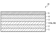
- FIG. 1 It is a schematic sectional drawing which shows one structural example of the magnetic recording medium of this invention. It is a schematic sectional drawing which shows another structural example of the magnetic recording medium of this invention.
- SEM scanning electron microscope
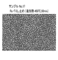
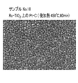
- FIG. 3 is a photograph observed by SEM after forming a Pt—C layer on a Ru—TiO 2 layer and heat-treating it at a heating temperature of 450 ° C. for a heating time of 60 minutes. Forming a Pt-TiO 2 layers of ru-TiO 2 layer on the heating temperature 450 ° C., after heat treatment at the heating time of 60 minutes, a photograph observed by SEM. Forming a Pt-TiO 2 layers of ru-TiO 2 layer on the further form a ZnO layer, a heating temperature 450 ° C., after heat treatment at the heating time of 60 minutes, a photograph observed by SEM. The grain density of the Pt layer on Ru—TiO 2 is shown.
- the Pt (111) peak intensity of X-ray diffraction (XRD) is shown. Is a SEM photograph showing a comparison between the Ta underlayer and Ru-TiO 2 base.
- FIG. 11 is a SEM photograph of a Ru-24 vol% TiO 2 stopper as a reference for FIG.
- the XRD result of the example of FIG. 10 is shown. It is a graph which shows a grain density when formation is stopped in each layer.
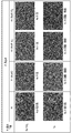
- the SEM observation result of Experimental example 4 is shown. It is a schematic sectional drawing which shows another structural example of the magnetic recording medium of this invention. It is the result of having observed the particle size of the nonmagnetic intermediate
- One example of a mode for carrying out the present invention is a magnetic recording including a substrate 1, a first seed layer 2, a second seed layer 3 containing ZnO, a third seed layer 4 containing MgO, and an ordered alloy.
- the magnetic recording medium 10 includes the layer 5 in this order, and the first seed layer 2 includes Ru and at least one selected from the group consisting of oxide, carbide, and nitride.
- a nonmagnetic intermediate layer 6 is further included between the first seed layer 2 and the second seed layer 3, and the nonmagnetic intermediate layer 6 is made of Pt and an oxide, carbon, carbide, and nitride group. And at least one selected from.
- the nonmagnetic intermediate layer consists essentially of Pt, and the nonmagnetic intermediate layer has a thickness of 0.1 to 3.0 nm.
- the ordered alloy is a L1 0 type ordered alloy containing at least one element selected from Fe and Co, Pt, Pd, Au, and at least one element selected from the group consisting of Ir and Rh It is preferable.
- the ordered alloy preferably further includes at least one element selected from the group consisting of Ni, Mn, Cu, Ru, Ag, Au, and Cr.
- the magnetic recording layer 5 preferably has a granular structure including magnetic crystal grains and nonmagnetic crystal grain boundaries surrounding the magnetic crystal grains, and the magnetic crystal grains preferably include the ordered alloy.
- the nonmagnetic crystal grain boundary preferably includes a nonmagnetic material selected from the group consisting of carbon, oxide, and nitride.
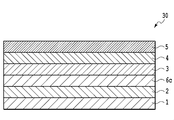
- FIG. 1 includes a substrate 1, a first seed layer 2, a second seed layer 3 containing ZnO, a third seed layer 4 containing MgO, and a magnetic recording layer 5 containing an ordered alloy in this order.
- One configuration example of the magnetic recording medium 10 in which one seed layer 2 includes Ru and at least one selected from the group consisting of oxide, carbide, and nitride is shown.
- the same reference numerals are given to common components, and the description thereof is omitted.
- a notation such as A / B means that A is the upper layer and B is the lower layer.
- the substrate 1 may be various plate-like members having a smooth surface.
- the substrate 1 can be formed using a material generally used for magnetic recording media. Materials that can be used include Al alloys plated with NiP, MgO single crystals, MgAl 2 O 4 , SrTiO 3 , tempered glass, crystallized glass and the like.
- an adhesion layer may be provided between the substrate 1 and the first seed layer 2 described in detail later.
- an adhesion layer (not shown) may be provided.
- the adhesion layer is used to enhance adhesion between a layer formed on the adhesion layer and a layer formed under the adhesion layer.
- the layer formed under the adhesion layer includes the substrate 1.
- the material for forming the adhesion layer includes metals such as Ni, W, Ta, Cr, and Ru, and alloys containing the aforementioned metals.
- the adhesion layer may be a single layer or may have a laminated structure of a plurality of layers.
- a preferable adhesion layer in this configuration example is made of CrTi.
- a soft magnetic backing layer (not shown) may be provided.
- the soft magnetic underlayer controls the magnetic flux from the magnetic head to improve the recording / reproducing characteristics of the magnetic recording medium.
- Materials for forming the soft magnetic backing layer include NiFe alloys, Sendust (FeSiAl) alloys, crystalline materials such as CoFe alloys, microcrystalline materials such as FeTaC, CoFeNi, CoNiP, and Co alloys such as CoZrNb and CoTaZr. Includes amorphous material.
- the optimum value of the thickness of the soft magnetic backing layer depends on the structure and characteristics of the magnetic head used for magnetic recording. When the soft magnetic backing layer is formed continuously with the other layers, the soft magnetic backing layer preferably has a thickness in the range of 10 nm to 500 nm (including both ends) in consideration of productivity.
- a heat sink layer may be provided.
- the heat sink layer is a layer for effectively absorbing excess heat of the magnetic recording layer 5 generated during the heat-assisted magnetic recording.
- the heat sink layer can be formed using a material having high thermal conductivity and specific heat capacity.
- a material includes Cu simple substance, Ag simple substance, Au simple substance, or an alloy material mainly composed of them.
- “mainly” means that the content of the material is 50 wt% or more.
- the heat sink layer can be formed using an Al—Si alloy, a Cu—B alloy, or the like.
- the heat sink layer can be formed using Sendust (FeSiAl) alloy, soft magnetic CoFe alloy, or the like.
- Sendust FeSiAl
- soft magnetic material By using a soft magnetic material, the function of concentrating the perpendicular magnetic field generated by the head on the magnetic recording layer 5 can be imparted to the heat sink layer, and the function of the soft magnetic backing layer can be supplemented.
- the optimum value of the thickness of the heat sink layer varies depending on the heat quantity and heat distribution during heat-assisted magnetic recording, the layer configuration of the magnetic recording medium, and the thickness of each component layer. In the case of continuously forming with other constituent layers, the thickness of the heat sink layer is preferably 10 nm or more and 100 nm or less in consideration of productivity.
- the heat sink layer can be formed using any method known in the art, such as a sputtering method or a vacuum evaporation method. Usually, the heat sink layer is formed using a sputtering method.
- the heat sink layer can be provided between the substrate 1 and the adhesion layer, between the adhesion layer and the orientation control layer, in consideration of characteristics required for the magnetic recording medium.
- an orientation control layer (not shown) may be provided.
- the orientation control layer is a layer for forming a (002) -oriented hcp structure in the first seed layer 2 described later.
- the orientation control layer is formed under the first seed layer 2.
- the orientation control layer may be a single layer or may have a laminated structure of a plurality of layers.
- the material that can be used for forming the orientation control layer is preferably a material having an hcp structure or a face-centered cubic (fcc) structure that is the same crystal structure as the magnetic recording layer, but is not limited thereto. is not.
- materials that can be used to form the orientation control layer include Ru or Ru alloys, Co—Ni alloys, Ni alloys, Pt alloys, Pd alloys, Ta alloys, Cr alloys, Si alloys, and Cu alloys.
- the material further includes one or more elements selected from the group consisting of Ru, W, Mo, Ta, Nb, and Ti for the purpose of improving the consistency of the crystal lattice size with the seed layer. But you can.
- the material may further include one or more materials selected from the group consisting of B, Mn, Al, Si oxide, and Ti oxide.
- a preferred orientation control layer in this configuration example has a NiW alloy layer, a Ru layer, or a laminated structure thereof.
- the orientation control layer can be formed using any method known in the art such as sputtering.
- the total thickness of the orientation control layer is preferably 1 to 20 nm from the viewpoint of the orientation of the first seed layer.
- the first seed layer 2 includes Ru and at least one selected from the group consisting of oxides, carbides, and nitrides.
- at least one selected from the group consisting of oxides, carbides, and nitrides included with Ru can also be called a grain boundary material.
- the grain boundary material may be, for example, an oxide such as SiO 2 , TiO 2 , or ZnO, a carbide such as SiC, TiC, or WC, or a nitride such as SiN or TiN.
- the oxide or the like as an impurity included in the first seed layer 2 is clearly distinguished from at least one selected from the group consisting of oxide, carbide, and nitride included with Ru.
- at least one selected from the group consisting of oxide, carbide, and nitride is, for example, 5% by volume or more based on the total amount of Ru, it is included in the first seed layer 2 together with Ru. Can do.
- the first seed layer 2 typically has a hexagonal wurtzite structure in which the second seed layer 3 is (002) -oriented with a small crystal orientation dispersion and leads to a good granular structure up to the magnetic recording layer 5.
- This granular structure is a structure in which individual crystal grains are surrounded by another material in a plane parallel to the substrate, and in the cross section perpendicular to the substrate, the individual crystal grains have a columnar structure. Is preferred. More specifically, in a cross section perpendicular to the substrate, it is preferable that no grain boundary material is formed on the upper and lower portions of each crystal grain. In this case, Ru corresponds to a crystal grain.
- the first seed layer 2 can be formed by any method known in the art such as sputtering.
- the first seed layer 2 typically includes Ru—TiO 2 or Ru—SiO 2 .
- the first seed layer 2 containing Ru—TiO 2 or the like preferably has a granular structure. This granular structure is a state in which a grain boundary material such as TiO 2 is segregated so as to surround the periphery of the Ru crystal grains in a plane parallel to the substrate.
- the Ru-TiO 2 specifically a phenomenon where Ru and TiO 2 were coexisting
- the Ru-SiO 2 means a state in which Ru and SiO 2 were coexist.
- the first seed layer may be a single layer or a multilayer. Layers having different grain boundary materials may be stacked, or layers of grain boundary materials having different concentrations may be stacked.
- the nonmagnetic intermediate layer may include Pt and at least one selected from the group consisting of oxide, carbon, carbide, and nitride.
- the nonmagnetic intermediate layer may include Pt and at least one selected from the group consisting of oxide, carbon, carbide, and nitride.
- at least one selected from the group consisting of oxide, carbon, carbide, and nitride included with Pt can also be called a grain boundary material, for example, an oxide such as SiO 2 , TiO 2 , or ZnO, Carbides such as carbon (C), SiC, TiC, and WC, and nitrides such as SiN and TiN can be used.
- the oxide or the like as an impurity contained in the nonmagnetic intermediate layer is clearly at least one selected from the group consisting of oxide, carbon (C), carbide, and nitride contained together with Pt. Differentiated. When at least one selected from the group consisting of oxide, carbon, carbide, and nitride is, for example, 5% by volume or more based on the total amount of Pt, it is included in the nonmagnetic intermediate layer together with Pt. be able to.
- a nonmagnetic intermediate layer 6 made of Pt—C or Pt—TiO 2 may be provided between the first seed layer 2 and the second seed layer 3 described in detail later.
- the nonmagnetic intermediate layer 6 (see FIG. 2) is a layer for promoting epitaxial growth of layers formed after the second seed layer 3.
- the nonmagnetic intermediate layer 6 can form a granular structure of the second seed layer 3 inherited from the first seed layer 2.
- the nonmagnetic intermediate layer 6 can be formed by using any method known in the art such as sputtering.
- the nonmagnetic intermediate layer 6 containing Pt—TiO 2 or the like preferably has a granular structure.
- Pt—C means a state in which Pt and carbon (C) coexist.
- the nonmagnetic intermediate layer may be a single layer or a multilayer. Layers having different grain boundary materials may be stacked, or layers of grain boundary materials having different concentrations may be stacked.
- a nonmagnetic intermediate layer consisting essentially of Pt is provided between the first seed layer 2 and the second seed layer 3 described in detail later, and the nonmagnetic intermediate layer has a thickness of 0.1 to 3.0 nm. It is preferable to have a film thickness.
- the nonmagnetic intermediate layer has a thickness of more preferably 0.5 to 2.5 nm, and still more preferably 0.5 to 2.0 nm. Most preferably, it has a thickness of 0.5 to 1.5 nm.
- the nonmagnetic interlayer consists essentially of Pt
- the nonmagnetic interlayer typically does not include a grain boundary material.
- A consists essentially of B
- A may include, for example, additional C in addition to B, but that additional C does not substantially affect the characteristics of A. Used to do. Further typical examples of C are impurities and the like which are mixed unintentionally. If it is the range of the said film thickness, the granular structure of a 1st seed layer can be maintained without breaking.
- the second seed layer 3 contains ZnO.
- the second seed layer 3 preferably contains 70 wt% or more of ZnO.
- ZnO may have a stoichiometric composition or a non-stoichiometric composition.
- ZnO in the second seed layer 3 typically has a (002) -oriented hexagonal wurtzite crystal structure.
- the second seed layer 3 has an effect of forming a sodium chloride type structure in which the third seed layer 4 containing MgO is (002) -oriented on the first seed layer 2 having the (002) plane of the hcp structure. Further, it can be considered that the presence of the second seed layer 3 has an effect of reducing the crystal orientation dispersion of the magnetic recording layer 5 even when the third seed layer 4 is thin. Further, in order to guide the crystal grain separation structure of the first seed layer 2 to the third seed layer 4, the thickness must not be excessively increased. In order to achieve the above effect, the second seed layer 3 preferably has a thickness in the range of 1 nm to 20 nm.
- the third seed layer 4 improves the degree of order of the magnetic recording layer 5 made of an ordered alloy formed thereon. Further, the third seed layer 4 is considered to guide the separation structure of the crystal grains of the second seed layer 3 to the magnetic recording layer 5 and promote the separation of the magnetic crystal grains in the magnetic recording layer 5. In order to achieve the above effect, the third seed layer 4 preferably has a thickness in the range of 1 nm to 20 nm.
- the second seed layer 3 and the third seed layer 4 can be formed using any method known in the art such as sputtering.
- sputtering it is preferable to set the temperature of the board
- the second seed layer 3 containing ZnO it is not necessary to heat the substrate 1 at the time of formation.
- the second seed layer 3 formed without heating the substrate 1 can achieve a surface roughness equal to or lower than that of the third seed layer 4 formed with heating of the substrate 1.
- the crystal orientation of the ordered alloy in the magnetic recording layer 5 is appropriately oriented to the magnetic recording medium. It becomes possible. In particular it is possible to correct (001) orientation of the crystal orientation of the L1 0 type ordered alloy perpendicular magnetic recording medium.
- the magnetic recording layer 5 includes an ordered alloy.
- the ordered alloy includes at least one first element selected from the group consisting of Fe and Co, and at least one second element selected from the group consisting of Pt, Pd, Au, Ir, and Rh.
- Preferred ordered alloy is FePt, CoPt, FePd, and L1 0 type ordered alloy selected from the group consisting of CoPd.
- the ordered alloy may further include at least one element selected from the group consisting of Ni, Mn, Cu, Ru, Ag, Au, and Cr. Desirable property modulation includes a decrease in temperature required for ordering of the ordered alloy.
- the ratio of the first element to the second element may be within the range of 0.7 to 1.3, preferably within the range of 0.8 to 1.1, based on the number of atoms. Good. By using the composition ratio within this range, it is possible to obtain L1 0 ordered structure having a large magnetic anisotropy constant Ku.
- the magnetic recording layer 5 may have a granular structure including magnetic crystal grains and nonmagnetic crystal grain boundaries surrounding the magnetic crystal grains.
- the magnetic crystal grain may include the ordered alloy described above.
- the nonmagnetic crystal grain boundary may include materials such as oxides such as SiO 2 , TiO 2 , and ZnO, nitrides such as SiN and TiN, carbon (C), and boron (B).
- the magnetic recording layer 5 may be composed of a plurality of magnetic layers. Each of the plurality of magnetic layers may have a non-granular structure or a granular structure. Furthermore, an ECC (Exchange-coupled Composite) structure in which a coupling layer such as Ru is sandwiched between magnetic layers may be provided. Further, the second magnetic layer may be provided on the upper part of the magnetic layer having the granular structure as a continuous layer (CAP layer) not including the granular structure.
- ECC Exchange-coupled Composite
- the magnetic recording layer 5 can be formed by depositing a predetermined material by a sputtering method.
- a target including a material forming the ordered alloy can be used. More specifically, it is possible to use a target containing the elements constituting the ordered alloy described above at a predetermined ratio.
- the magnetic recording layer 5 may be formed by using a plurality of targets containing a single element and adjusting the power applied to each target to control the ratio of the elements.
- a target including a material that forms magnetic crystal grains and a material that forms nonmagnetic crystal grain boundaries in a predetermined ratio can be used.
- a target including a material that forms magnetic crystal grains and a target including a material that forms nonmagnetic crystal grain boundaries can be used.
- the magnetic recording layer 5 may be formed by adjusting the power applied to each of these targets to control the constituent ratio of the magnetic crystal grains and the nonmagnetic crystal grain boundaries.
- a plurality of targets separately containing elements constituting the ordered alloy may be used.
- the substrate 1 is heated when the magnetic recording layer 5 is formed. At this time, the temperature of the substrate 1 is in the range of 300 ° C. to 600 ° C. By adopting the temperature of the substrate 1 within this range, the degree of order of the ordered alloy in the magnetic recording layer 5 can be improved. Because it is 300 ° C. or higher, there is an effect that it is possible to improve the degree of order of L1 0 ordered alloy. Since it is 600 degrees C or less, there exists an effect of suppressing surface roughness.
- a protective layer (not shown) may be provided.
- the protective layer can be formed using a material conventionally used in the field of magnetic recording media.
- the protective layer can be formed using a nonmagnetic metal such as Pt, a carbon-based material such as diamond-like carbon, or a silicon-based material such as silicon nitride.
- the protective layer may be a single layer or may have a laminated structure of a plurality of layers.
- the protective layer having a laminated structure may be, for example, a laminated structure of two types of carbon materials having different characteristics, a laminated structure of metals and carbon materials, or a laminated structure of metal oxide layers and carbon materials.
- the protective layer can be formed using any method known in the art, such as sputtering, CVD, and vacuum deposition.
- a liquid lubricant layer (not shown) may be provided.
- the liquid lubricant layer can be formed using a material conventionally used in the field of magnetic recording media.
- a perfluoropolyether lubricant can be used.
- the liquid lubricant layer can be formed using, for example, a coating method such as a dip coating method or a spin coating method.
- Experimental Example 1 is an experimental example of the Ru-TiO 2 first seed layer 2.
- the eight sample Nos. Created Details of 1 to 8 are shown in Table 1.
- Sample No. Reference numerals 1 and 2 are samples in which a 5.9 nm Ru layer is formed on a glass substrate.
- the amount of TiO 2 added to the Ru—TiO 2 layer was 24 vol% based on the total volume of Ru.
- the Ru—TiO 2 layer has three thicknesses of 0.65, 1.3, and 2.6 nm. Of these, only the even-numbered samples were subjected to heat treatment.
- the heating temperature was 450 ° C., which is the temperature during normal formation of FePt, and the heating time was 60 minutes.
- the particle size is the diameter of the particles surrounded by the grain boundary material generated on the sample surface.
- the particle size is analyzed as an equivalent circle diameter from an image obtained by SEM observation using image analysis software (trade name: WinRoof, manufactured by Mitani Corporation), and the average particle size (D), standard deviation ( ⁇ ), The grain density was derived.
- the grain density is the average number of grains per 10,000 nm 2 .
- Example No. 1, 2 A specific sample preparation procedure will be described. First, a chemically strengthened glass substrate (N-10 glass substrate manufactured by HOYA) having a smooth surface was washed to prepare a substrate. The cleaned substrate was introduced into an in-line type sputtering apparatus.
- a chemically strengthened glass substrate N-10 glass substrate manufactured by HOYA having a smooth surface was washed to prepare a substrate. The cleaned substrate was introduced into an in-line type sputtering apparatus.
- a CrTi layer having a thickness of 15 nm was first formed by a DC magnetron sputtering method using a Cr 50 Ti 50 target as an adhesion layer.
- a 5 nm thick RuCr first orientation control layer was formed by DC magnetron sputtering using a Ru 70 Cr 30 target.
- a Ru second orientation control layer having a thickness of 5.9 nm was formed by DC magnetron sputtering using a Ru target.
- the substrate temperature was room temperature (25 ° C.) in Ar gas at a pressure of 0.3 Pa.
- the sputtering power when forming the Ru orientation control layer was 200 W. As described above, sample no. 1-2 were created.
- Sample Nos. 3 to 8 A specific sample preparation procedure will be described. Sample No. First, similarly to 1 and 2, a chemically strengthened glass substrate (N-10 glass substrate manufactured by HOYA) having a smooth surface was washed to prepare a substrate. The cleaned substrate was introduced into an in-line type sputtering apparatus.
- N-10 glass substrate manufactured by HOYA a chemically strengthened glass substrate having a smooth surface was washed to prepare a substrate. The cleaned substrate was introduced into an in-line type sputtering apparatus.
- a CrTi layer having a thickness of 15 nm was first formed by a DC magnetron sputtering method using a Cr 50 Ti 50 target as an adhesion layer.
- a 5 nm thick RuCr first orientation control layer was formed by DC magnetron sputtering using a Ru 70 Cr 30 target.
- a Ru second orientation control layer having a thickness of 5.9 nm was formed by DC magnetron sputtering using a Ru target.
- the substrate temperature was room temperature (25 ° C.) in Ar gas at a pressure of 0.3 Pa.
- the sputtering power when forming the Ru orientation control layer was 200 W.
- a Ru—TiO 2 first seed layer having a thickness of 0.65 to 2.6 nm was formed by DC magnetron sputtering using an Ru-24 vol% TiO 2 target in Ar gas at a pressure of 0.3 Pa (sample). No. 3 to 8).
- the substrate temperature in ru-TiO 2 first seed layer formed was room temperature (25 ° C.).
- the sputtering power when forming the Ru—TiO 2 first seed layer was 50 W. As described above, sample no. 3 to 8 were created.
- the average particle size of the sample in which the magnetic recording layer was not formed and heat-treated was 6.4 to 6.5 nm.
- the Ru—TiO 2 layer was formed, there was no significant change in the particle size with and without heat treatment.
- No. 2 abnormal coarsening of Ru grains was observed.
- the particle size could not be measured with this sample.
- the Ru—TiO 2 first seed layer formed on the Ru layer of the second orientation control layer has an effect of suppressing the coarsening of the Ru grains due to heating. Even if a Ru—TiO 2 layer is formed on the substrate, the coarsening of the Ru particles is suppressed, and it is expected that the same effect can be obtained. That is, it is considered that the coarsening of the Ru particles is suppressed because the TiO 2 or the like surrounds the fine Ru particles. Since fine Ru particles can be maintained, magnetic particles grown one-on-one can be made fine particles. Similar effects were obtained not only in the Ru—TiO 2 layer but also in the Ru—SiO 2 layer.
- the particle structure of the Ru-TiO 2 layer or Ru-SiO 2 layer when FePt magnetic recording layer is epitaxially grown, by receiving the granular structure of the Ru-TiO 2 layer, the magnetic particles take clean granular structure Will be able to.
- the structure in which the particles such as oxide are surrounded by Ru can receive the magnetic particles so that the magnetic particles can have a clean structure.
- coarsening of Ru particles in the orientation control layer due to heat treatment when forming the magnetic recording layer is suppressed. That is, Ru does not become coarse even when heated when forming the magnetic recording layer, and miniaturization is possible.
- One-to-one growth of each layer particle is possible from the seed layer or orientation control layer to the magnetic recording layer.
- Experimental example 2 includes a Ru—TiO 2 first seed layer 2, a ZnO second seed layer 3, and a MgO third seed layer 4, and further includes a Ru—TiO 2 first seed layer 2 and a ZnO second seed layer 3.
- Experimental Example 2 in the layer structure of ZnO layer / Pt layer / Ru-TiO 2 layer, the addition of grain boundaries material Pt layer, Pt layer, to consider whether the particle aggregation by heating in ZnO layer is suppressed Is.
- an adhesion layer and an orientation control layer were provided between the glass substrate and the first seed layer.
- a CrTi layer having a thickness of 15 nm was first formed by a DC magnetron sputtering method using a Cr 50 Ti 50 target as an adhesion layer underlayer.
- a Ru alignment control layer having a thickness of 10 nm was formed as a first alignment control layer by DC magnetron sputtering using a Ru target.
- Table 2 shows conditions for forming a layer using Pt, Pt—C, or Pt—TiO 2 as the nonmagnetic intermediate layer. After the formation of the nonmagnetic intermediate layer, post-heating was performed at 450 ° C. for 60 minutes.
- Table 3 shows the structure of each sample. In Table 3, for example, a sample of Ru—TiO 2 / Ru / adhesion layer / glass substrate means that after heating to Ru—TiO 2 , post heating 450 ° C. ⁇ 60 min was performed.
- the evaluation method was surface observation by SEM. Photographs observed by SEM are shown in FIGS. Generally, in order to order FePt, it is necessary to form a layer at a high temperature. However, when the film thickness of the Pt layer was 8 nm and no grain boundary material was added, it was confirmed that Pt agglomerates due to heating and cannot inherit the Ru particle diameter of the first seed layer. On the other hand, it was confirmed that the grain size of Ru in the orientation control layer and the first seed layer can be inherited by adding a grain boundary material (C or TiO 2 in this experimental example). Note that the sample numbers shown in FIGS. Is a sample No. described in Table 5 below. It corresponds to.
- Table 4 shows conditions when ZnO is formed on the Pt layer, Pt—C layer, or Pt—TiO 2 layer, which is the nonmagnetic intermediate layer. After the formation of the layer, post heating 450 ° C. ⁇ 60 min was performed.
- the Pt—C nonmagnetic intermediate layer or the Pt—TiO 2 nonmagnetic intermediate layer suppresses particle aggregation of the orientation control layer and the first seed layer even by heating during the formation of the magnetic layer. . It was confirmed that the particle diameters of the orientation control layer and the first seed layer can be maintained even after post-heating.
- the layer structure of ZnO / Pt layer / Ru—TiO 2 granular using the hcp-Ru (001) granular first seed layer a grain boundary material is added to the Pt layer, and the ZnO / Pt granular / Ru—TiO 2 is added. If the two- layer structure is used, particle aggregation of the seed layer due to heating during formation of the magnetic recording layer can be suppressed, and the particle size of the seed layer can be maintained even after post-heating.
- Experimental Example 3 is an experimental example for confirming the effect of the Ru—TiO 2 first seed layer.
- the layer structure in the experimental example is Pt—X layer / Ru—TiO 2 layer / Ru orientation control layer / adhesion layer / substrate.
- the experimental conditions up to the formation of the Ru—TiO 2 first seed layer were the same as in Experimental Example 2.
- the grain shapes of the Ru—TiO 2 first seed layer and the Pt layer (Pt, Pt-24 vol% C, or Pt-24 vol% TiO 2 ) formed on the Ta first seed layer as a comparison object were compared and examined. .
- an increase in the amount of TiO 2 added 24 ⁇ 30 vol%) was studied in part.
- FIG. 10 shows an SEM photograph observing the comparison between the Ta first seed layer and the Ru—TiO 2 first seed layer.
- FIG. 11 shows an SEM photograph of the Ru-24 vol% TiO 2 stopper substrate as a reference for FIG.
- stop means that the formation of further layers after that layer is stopped.
- Ru-TiO 2 stop sub in the table, on the glass substrate, means a state of forming to Ru-TiO 2 layers.
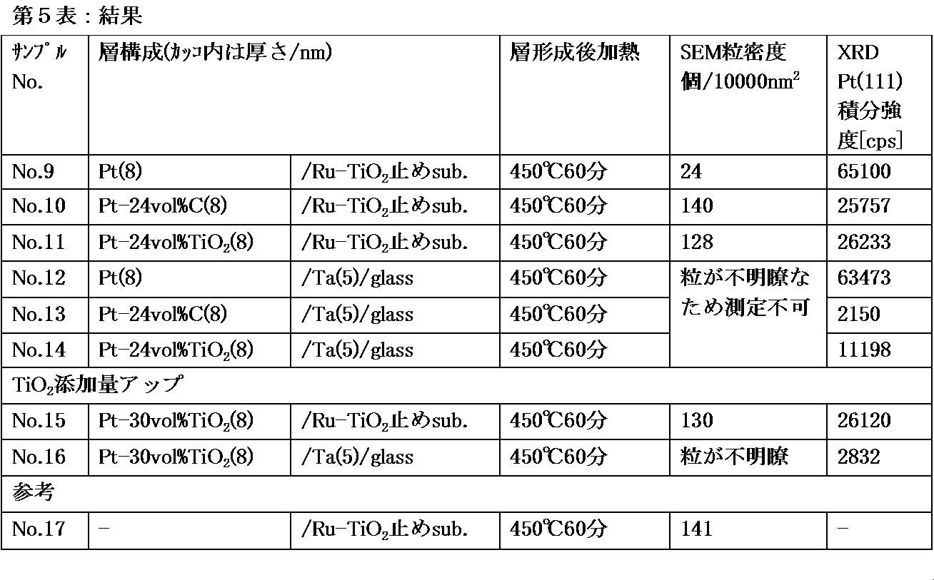
- good in FIG. 10 means that the particle diameter is about 5 to 10 nm. Sample No. In the Ta layers of 12 to 14 and 16, it was confirmed from FIG. 10 that the grains were unclear and the Pt particles were not sufficiently separated.
- FIG. 8 shows the grain density of the Pt layer on Ru—TiO 2 .
- Sample No. With 11 Pt-24 vol% TiO 2 the grain density decreased. Relatively small particles were reduced, resulting in a uniform particle size distribution. Sample No. Even if it was 30 vol% of 15, the result did not change so much.
- the XRD results of the samples in Table 5 are shown in FIG. This is an XRD profile obtained by ⁇ -2 ⁇ measurement in the perpendicular direction using X-ray diffraction.
- the perpendicular of the one-dot chain line with 2 ⁇ of 39.76 degrees is the (111) Pt peak position due to the Pt nonmagnetic intermediate layer
- the one-dot chain line perpendicular to 85.71 degrees is the Pt nonmagnetic intermediate layer.
- FIG. 9 shows the Pt (111) peak intensity of the X-ray diffraction (XRD) of FIG.
- XRD X-ray diffraction
- Experimental Example 4 is an experimental example aimed at confirming the crystal grain separation structure from the Ru—TiO 2 first seed layer to the FePt—C layer.
- the actual layer structure is FePt—C layer / MgO layer / ZnO layer / Pt—TiO 2 layer / Ru—TiO 2 layer / Ru orientation control layer / underlayer / substrate.
- the experimental conditions up to the formation of the Ru—TiO 2 layer were the same as in Experimental Example 2.
- Reference numeral 20 is a sample in which post-heating was performed at 450 ° C. for 60 minutes after all layers of each sample were formed.
- the MgO and FePt—C were formed by heating to 400 ° C.
- FIG. 13 is a graph showing the grain density at this time. Sample No. 17 and sample no. 18 is the same sample.
- the grain density is almost constant up to the Ru—TiO 2 layer, MgO layer, and magnetic layer even by heating when forming the third seed layer and the magnetic layer, and it is good influenced by the lower layer. It has been confirmed that a granular structure has been formed.
- Example 5 In order to increase the recording density of the heat-assisted magnetic recording medium, it is preferable to reduce the magnetic particle diameter of the magnetic recording layer to 6 nm or less. For the miniaturization of the magnetic recording layer, it is effective to make the seed layer formed under the magnetic recording layer fine.
- a magnetic recording medium including a magnetic recording layer / third seed layer (MgO) / second seed layer (ZnO) / nonmagnetic intermediate layer (Pt + grain boundary material) / first seed layer (Ru + grain boundary material)
- the grain boundary material contained in the nonmagnetic intermediate layer has the effect of suppressing grain size enlargement, but the crystal orientation of the second seed layer (ZnO seed layer), which is the original role of the nonmagnetic intermediate layer, is improved. The effect may be deteriorated.
- Experimental Example 5 is an experimental example for the purpose of confirming the structure of the nonmagnetic intermediate layer consisting essentially of Pt.
- FIG. 15 shows a magnetic recording medium 30 including a nonmagnetic intermediate layer 6c consisting essentially of Pt.
- the multilayer thin film shown in the following Tables 7 and 8 was formed by sputtering. Each sample was post-heated at 400 ° C. for 60 minutes after film formation for the purpose of following the film formation process of the MgO seed layer and the magnetic recording layer.
- the reference example has a configuration in which Pt-24 vol% TiO 2 including a grain boundary material is employed as the nonmagnetic intermediate layer, and this reference example was fabricated and evaluated. The film formation process of the reference example was the same as that of Experimental example 5.
- the ZnO (002) integrated intensity is an integrated intensity value of a peak having 2 ⁇ of 33.4 to 35.4 degrees due to ZnO (002) in the XRD profile.
- the particle diameter of the nonmagnetic intermediate layer is easily reflected in the magnetic particle diameter of the magnetic recording layer as it is. Accordingly, in order to achieve a magnetic particle diameter of 6 nm or less, it is preferable that the particle diameter of the nonmagnetic intermediate layer serving as the base is also 6 nm or less. As shown in FIG. 16, when Pt was used as the nonmagnetic intermediate layer, the particle size was almost the same when the film thickness was up to 2 nm as compared with the case of Pt—TiO 2 .
- the film thickness is 4 nm or more, Pt aggregates and a granular structure cannot be seen.
- the particle size enlargement was suppressed up to 2 nm of the nonmagnetic intermediate layer thickness, and a particle size of 6 nm could be achieved.
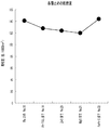
- the film thickness of the nonmagnetic intermediate layer is greater in the case of using either the Pt or Pt—TiO 2 nonmagnetic intermediate layer than in the case where the nonmagnetic intermediate layer is not used (integrated intensity of 0 nm in FIG. 17).
- the film thickness up to 2 nm higher strength was shown. This indicates that the crystal orientation is improved. From the above, it was found that a fine particle diameter of 6 nm or less and a good crystal orientation can be compatible by setting Pt as a nonmagnetic intermediate layer and a film thickness of 2 nm. In this experimental example, the result is a film thickness of 0.5 to 2 nm, but the same effect can be obtained with a film thickness of 0.1 to 3 nm.
- the first seed layer made of Ru to which the grain boundary material is added and the Pt nonmagnetic intermediate layer having a film thickness of 0.1 to 3 nm or less are combined, additional grain boundary material is added to the Pt nonmagnetic intermediate layer. It was found that even if it was not, it would not be a continuous film but would have an island structure. It is considered that the grain boundary width is secured in the first seed layer, the film thickness of the nonmagnetic intermediate layer is thin, and Pt does not aggregate due to these factors. When the thickness of the Pt nonmagnetic intermediate layer is thin, Pt is selectively formed in the top portion of each Ru particle in the first seed layer. That is, Pt is not continuously formed between adjacent Rus, but is formed separately.
- the crystal orientation of the ZnO seed can be further improved as compared with the case where the nonmagnetic intermediate layer is not used, similarly to the configuration using the Pt + grain boundary material for the nonmagnetic intermediate layer.
- the fine particle size ( ⁇ 6 nm) and good crystal orientation can be compatible.
Landscapes
- Engineering & Computer Science (AREA)
- Manufacturing & Machinery (AREA)
- Magnetic Record Carriers (AREA)
- Manufacturing Of Magnetic Record Carriers (AREA)
- Thin Magnetic Films (AREA)
Abstract
Description
実験例1は、Ru-TiO2第1シード層2の実験例である。作成した8種類のサンプルNo.1~8の詳細を第1表に示す。サンプルNo.1~2は、ガラス基板上に5.9nmのRu層が形成されたサンプルである。サンプルNo.3~8はさらにその上にRu-TiO2層を0.65~2.6nm形成したものである。Ru-TiO2層のTiO2添加量はRuの全体体積を基準として24vol(体積)%とした。Ru-TiO2層の厚さは0.65、1.3、2.6nmの3種類とした。これらの内、偶数番のサンプルについてのみ加熱処理を行なった。加熱温度はFePtの通常の形成時の温度である450℃とし、加熱時間は60分とした。作製したサンプルについて走査電子顕微鏡(SEM)により表面形状を観察し、粒径を計測した。なお、粒径とは、前記サンプル表面に生じた粒界材料で取り囲まれた粒子の直径である。具体的には、粒径はSEM観察による画像から画像解析ソフトウェア(三谷商事株式会社製、商品名:WinRoof)により、円相当径として解析し、平均粒径(D)、標準偏差(σ)、粒密度を導出した。なお、前記粒密度は10000nm2当りの平均の粒の個数である。

具体的なサンプル作製手順を説明する。最初に、平滑な表面を有する化学強化ガラス基板(HOYA社製N-10ガラス基板)を洗浄し、基板を準備した。洗浄後の基板を、インライン式のスパッタ装置内に導入した。
具体的なサンプル作製手順を説明する。サンプルNo.1,2と同様に最初に、平滑な表面を有する化学強化ガラス基板(HOYA社製N-10ガラス基板)を洗浄し、基板を準備した。洗浄後の基板を、インライン式のスパッタ装置内に導入した。
実験例2は、Ru-TiO2第1シード層2、ZnO第2シード層3、およびMgO第3シード層4を含み、更にRu-TiO2第1シード層2とZnO第2シード層3との間にPt-C非磁性中間層6aまたはPt-TiO2非磁性中間層6bを含む磁気記録媒体20に関する実験例である。実験例2は、ZnO層/Pt層/Ru-TiO2層の層構成において、Pt層に粒界材料を添加することで、Pt層、ZnO層における加熱による粒の凝集が抑えられるか検討するものである。特に、Ru配向制御層から結晶粒を1対1成長させ、FePt磁性粒子の粒径および粒径のばらつきを低減することを求めたものである。なお、前記実験例1と同様の方法で、ガラス基板と第1シード層の間に、密着層、配向制御層(Ru)を設けた。具体的には、最初に密着層下地層としてCr50Ti50ターゲットを用いたDCマグネトロンスパッタ法により厚さ15nmのCrTi層を形成した。次にRuターゲットを用いたDCマグネトロンスパッタ法により、第1配向制御層として、厚さ10nmのRuの配向制御層を形成した。



実験例3は、Ru-TiO2第1シード層の効果を確認するための実験例である。実験例での層構成はPt-X層/Ru-TiO2層/Ru配向制御層/密着層/基板である。Ru-TiO2第1シード層形成までの実験条件は実験例2と同様とした。Ru-TiO2第1シード層、および比較対象としてのTa第1シード層の上に形成したPt層(Pt、Pt-24vol%C、またはPt-24vol%TiO2)の粒形状を比較検討した。また、一部でTiO2添加量の増量(24→30vol%)を検討した。なお、各サンプルの層を形成後、後加熱450℃×60minを実施した。結果を第5表に示す。なお、表中のSEM粒密度は、1辺100nmの正方形範囲に入る粒子の個数を数えることにより求めた。
実験例4は、Ru-TiO2第1シード層からFePt-C層までの結晶粒の分離構造を確認することを目的とした実験例である。実際の層構成は、FePt-C層/MgO層/ZnO層/Pt-TiO2層/Ru-TiO2層/Ru配向制御層/下地層/基板である。Ru-TiO2層形成までの実験条件は実験例2と同様とした。なお、サンプルNo.18からサンプルNo.20は、各サンプルの層を全て形成した後、後加熱450℃×60minが実施されたサンプルである。また、前記MgO、FePt-Cは400℃に加熱して形成した。各層で止めたサンプルを形成し、各層までの粒構造を比較した。第6表および図14に実験例4のSEM観察結果を示す。図13はこの時の粒密度を示すグラフである。なお、サンプルNo.17とサンプルNo.18は同じサンプルである。

熱アシスト磁気記録媒体の高記録密度化のためには、磁気記録層の磁性粒子径を6nm以下に微細化することが好ましい。磁気記録層の微細化には、磁気記録層下に形成されるシード層の微粒子化が有効である。例えば、磁気記録層/第3シード層(MgO)/第2シード層(ZnO)/非磁性中間層(Pt+粒界材料)/第1シード層(Ru+粒界材料)を含む構成の磁気記録媒体においては、非磁性中間層に含まれる粒界材料は、粒径肥大化を抑制する効果があるが、非磁性中間層本来の役割である第2シード層(ZnOシード層)の結晶配向性改善効果を劣化させる場合がある。
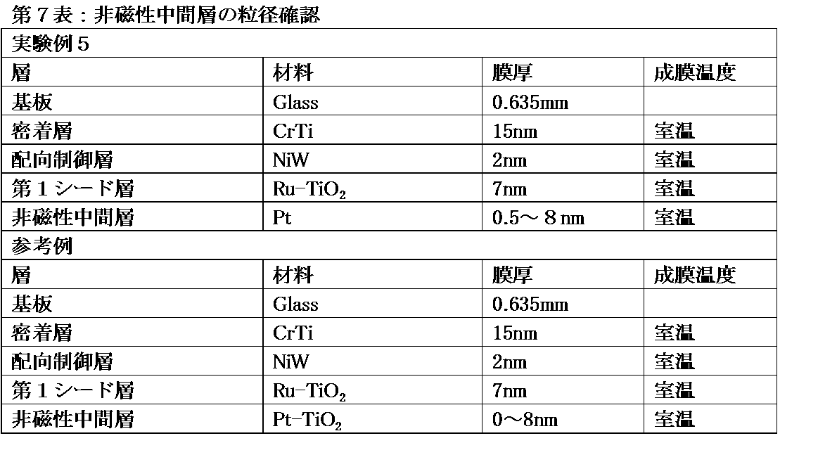
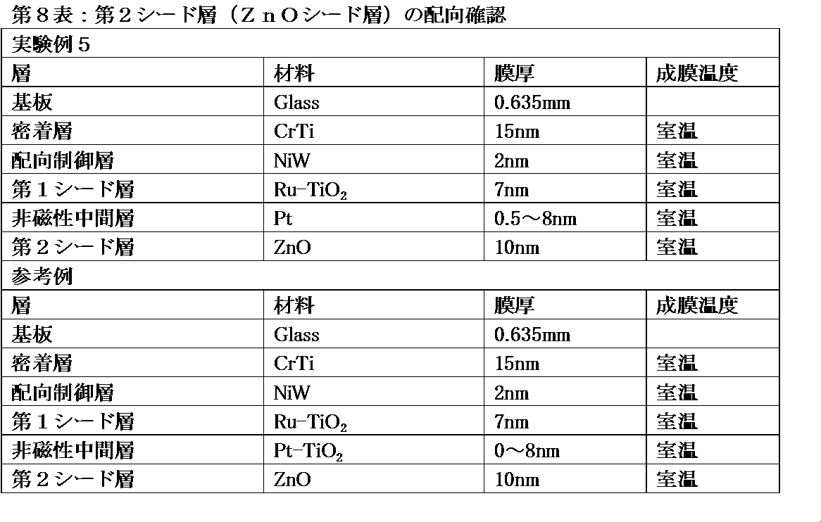
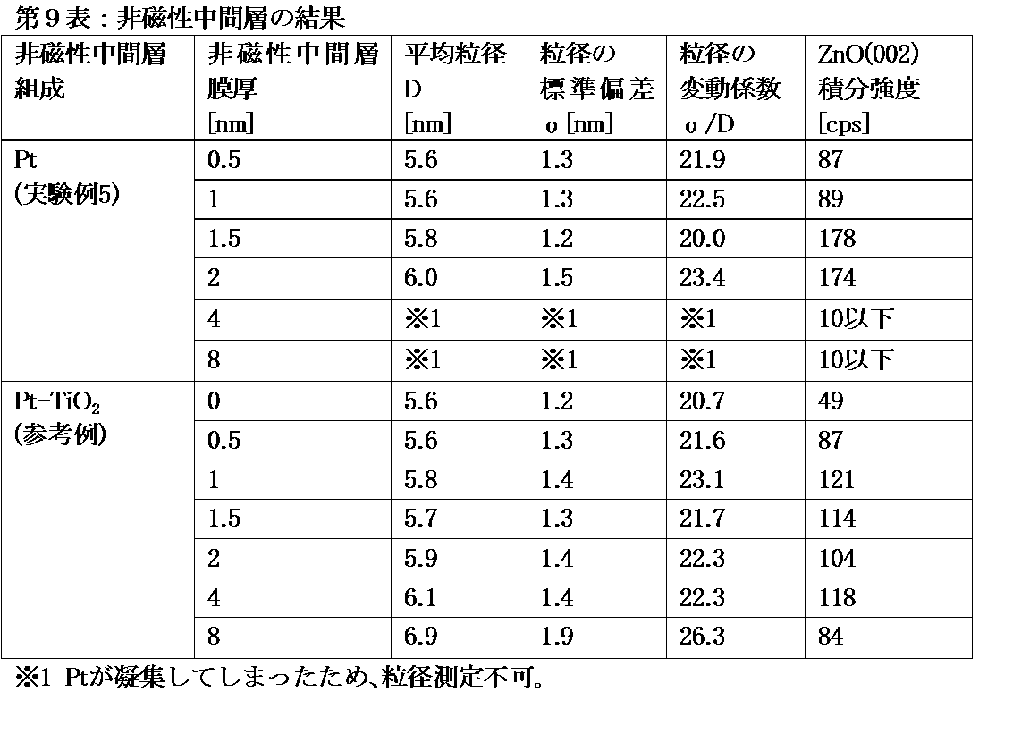
非磁性中間層を用いて、第1シード層から磁気記録層まで1対1の関係でエピタキシャル成長するとき、非磁性中間層の粒子径は磁気記録層の磁性粒子径にそのまま反映されやすい。従って磁性粒子径6nm以下を達成するためには、下地となる非磁性中間層の粒径も6nm以下とするのが好ましい。図16のように、Ptを非磁性中間層として用いた場合、Pt-TiO2の場合に対して、膜厚が2nmまでにおいては、その粒径はほぼ同等であった。しかしながら、膜厚が4nm以上のものでは、Ptが凝集してしまいグラニュラー構造が見られなくなっていた。非磁性中間層膜厚2nmまでは粒径肥大化が抑制されており、粒径6nmを達成できた。また、図17にように、Ptを非磁性中間層として用いた場合とPt-TiO2を用いた場合に対して、その直上に成膜される第2シード層(ZnOシード層)の結晶配向をZnO(002)ピークの積分強度で比較した。その結果、非磁性中間層を用いないもの(図17における膜厚0nmの積分強度)に比べて、Pt、Pt-TiO2どちらの非磁性中間層を用いた場合でも、非磁性中間層膜厚2nmまでの膜厚においては、より高い強度を示した。これは結晶配向が改善されていることを示している。以上から、Ptを非磁性中間層とし、その膜厚を2nmとすることで、6nm以下の微細粒子径と良好な結晶配向を両立できることが分かった。なお、本実験例では、膜厚0.5~2nmの結果であるが、膜厚0.1~3nmでも、同等の効果が得られる。
2 第1シード層
3 ZnOを含む第2シード層
4 MgOを含む第3シード層
5 磁気記録層
6 非磁性中間層
6a Pt-C非磁性中間層
6b Pt-TiO2非磁性中間層
6c Pt非磁性中間層
10、20、30 磁気記録媒体
Claims (20)
- 基板と、第1シード層と、ZnOを含む第2シード層と、MgOを含む第3シード層と、規則合金を含む磁気記録層とをこの順に含み、前記第1シード層が、Ruと、酸化物、炭化物、および窒化物からなる群から選択された少なくとも1つと、を含むことを特徴とする磁気記録媒体。
- 前記第1シード層が、Ruと、TiOm(m=1.5~2.5)またはSiOn(n=1.5~2.5)と、を含むことを特徴とする、請求項1に記載の磁気記録媒体。
- 前記第1シード層と前記第2シード層との間に非磁性中間層をさらに含み、前記非磁性中間層が、Ptと、酸化物、炭素、炭化物、および窒化物からなる群から選択された少なくとも1つと、を含むことを特徴とする請求項1に記載の磁気記録媒体。
- 前記非磁性中間層が、Ptと、TiOm(m=1.5~2.5)またはCと、を含むことを特徴とする請求項3に記載の磁気記録媒体。
- 前記第1シード層と前記第2シード層との間に非磁性中間層をさらに含み、前記非磁性中間層がPtから本質的になり、前記非磁性中間層が、0.1~3.0nmの膜厚を有することを特徴とする請求項1に記載の磁気記録媒体。
- 前記基板と前記第1シード層との間に、RuまたはRu合金から形成された配向制御層をさらに含むことを特徴とする請求項1に記載の磁気記録媒体。
- 前記規則合金は、FeおよびCoから選択される少なくとも一種の元素と、Pt、Pd、Au、Ir、およびRhからなる群から選択される少なくとも一種の元素とを含むL10型規則合金であることを特徴とする請求項1に記載の磁気記録媒体。
- 前記規則合金は、Ni、Mn、Cu、Ru、Ag、Au、およびCrからなる群から選択される少なくとも1種の元素をさらに含むことを特徴とする請求項7に記載の磁気記録媒体。
- 前記規則合金は、FePt、CoPt、FePd、およびCoPdからなる群から選択されるL10型規則合金であることを特徴とする請求項7に記載の磁気記録媒体。
- 前記磁気記録層が、磁性結晶粒と、前記磁性結晶粒を包囲する非磁性結晶粒界とを含むグラニュラー構造を有し、前記磁性結晶粒は前記規則合金を含むことを特徴とする請求項1に記載の磁気記録媒体。
- 磁気記録媒体を製造する方法であって、前記方法が、
基板を準備する工程と、
前記基板の上に第1シード層を形成する工程であって、前記第1シード層が、Ruと、酸化物、炭化物、および窒化物からなる群から選択された少なくとも1つと、を含む、工程と、
前記第1シード層の上にZnOを含む第2シード層を形成する工程と、
前記第2シード層の上にMgOを含む第3シード層を形成する工程と、
前記第3シード層の上に規則合金を含む磁気記録層を形成する工程とを含み、
前記磁気記録層を形成する際に、前記基板が300℃~600℃の範囲内で加熱される、方法。 - 前記第1シード層が、Ruと、TiOm(m=1.5~2.5)またはSiOn(n=1.5~2.5)と、を含むことを特徴とする、請求項11に記載の方法。
- 前記第1シード層と前記第2シード層との間に非磁性中間層を形成する工程をさらに含み、前記非磁性中間層が、Ptと、酸化物、炭素、炭化物、および窒化物からなる群から選択された少なくとも1つと、を含むことを特徴とする請求項11に記載の方法。
- 前記非磁性中間層が、Ptと、TiOm(m=1.5~2.5)またはCと、を含むことを特徴とする請求項13に記載の方法。
- 前記第1シード層と前記第2シード層との間に非磁性中間層を形成する工程をさらに含み、前記非磁性中間層がPtから本質的になり、前記非磁性中間層が、0.1~3.0nmの膜厚を有することを特徴とする請求項11に記載の方法。
- 前記基板と前記第1シード層との間に配向制御層を形成する工程を更に含み、前記配向制御層がRuまたはRu合金から形成されていることを特徴とする請求項11に記載の方法。
- 前記規則合金は、FeおよびCoから選択される少なくとも一種の元素と、Pt、Pd、Au、Ir、およびRhからなる群から選択される少なくとも一種の元素とを含むL10型規則合金であることを特徴とする請求項11に記載の方法。
- 前記規則合金は、Ni、Mn、Cu、Ru、Ag、Au、およびCrからなる群から選択される少なくとも1種の元素をさらに含むことを特徴とする請求項11に記載の方法。
- 前記規則合金は、FePt、CoPt、FePd、およびCoPdからなる群から選択されるL10型規則合金であることを特徴とする請求項11に記載の方法。
- 前記磁気記録層が、磁性結晶粒と、前記磁性結晶粒を包囲する非磁性結晶粒界とを含むグラニュラー構造を有し、前記磁性結晶粒は前記規則合金を含むことを特徴とする請求項11に記載の方法。
Priority Applications (4)
| Application Number | Priority Date | Filing Date | Title |
|---|---|---|---|
| SG11201710860RA SG11201710860RA (en) | 2016-01-12 | 2017-01-06 | Magnetic recording medium and method for producing same |
| JP2017561601A JP6304468B2 (ja) | 2016-01-12 | 2017-01-06 | 磁気記録媒体およびこれを製造する方法 |
| CN201780002234.1A CN107836022B (zh) | 2016-01-12 | 2017-01-06 | 磁记录介质及其制造方法 |
| US15/857,593 US10170145B2 (en) | 2016-01-12 | 2017-12-28 | Magnetic recording medium and method for producing the same |
Applications Claiming Priority (2)
| Application Number | Priority Date | Filing Date | Title |
|---|---|---|---|
| JP2016-003596 | 2016-01-12 | ||
| JP2016003596 | 2016-01-12 |
Related Child Applications (1)
| Application Number | Title | Priority Date | Filing Date |
|---|---|---|---|
| US15/857,593 Continuation US10170145B2 (en) | 2016-01-12 | 2017-12-28 | Magnetic recording medium and method for producing the same |
Publications (1)
| Publication Number | Publication Date |
|---|---|
| WO2017122593A1 true WO2017122593A1 (ja) | 2017-07-20 |
Family
ID=59311978
Family Applications (1)
| Application Number | Title | Priority Date | Filing Date |
|---|---|---|---|
| PCT/JP2017/000293 Ceased WO2017122593A1 (ja) | 2016-01-12 | 2017-01-06 | 磁気記録媒体およびこれを製造する方法 |
Country Status (6)
| Country | Link |
|---|---|
| US (1) | US10170145B2 (ja) |
| JP (1) | JP6304468B2 (ja) |
| CN (1) | CN107836022B (ja) |
| MY (1) | MY166236A (ja) |
| SG (1) | SG11201710860RA (ja) |
| WO (1) | WO2017122593A1 (ja) |
Cited By (2)
| Publication number | Priority date | Publication date | Assignee | Title |
|---|---|---|---|---|
| JP2020030880A (ja) * | 2017-03-10 | 2020-02-27 | 富士電機株式会社 | 磁気記録媒体 |
| JPWO2019065043A1 (ja) * | 2017-09-26 | 2020-11-05 | 富士フイルム株式会社 | 化合物の製造方法、組成物および硬化性組成物 |
Families Citing this family (1)
| Publication number | Priority date | Publication date | Assignee | Title |
|---|---|---|---|---|
| US10373637B2 (en) * | 2017-03-02 | 2019-08-06 | Seagate Technology Llc | Granularity in overlying magnetic and non-magnetic layers |
Citations (3)
| Publication number | Priority date | Publication date | Assignee | Title |
|---|---|---|---|---|
| JP2015026411A (ja) * | 2013-07-26 | 2015-02-05 | 昭和電工株式会社 | 磁気記録媒体および磁気記憶装置 |
| JP2015153447A (ja) * | 2014-02-18 | 2015-08-24 | 昭和電工株式会社 | 垂直磁気記録媒体、垂直磁気記録媒体の製造方法、垂直記録再生装置 |
| WO2016194383A1 (ja) * | 2015-06-02 | 2016-12-08 | 富士電機株式会社 | 磁気記録媒体の製造方法 |
Family Cites Families (8)
| Publication number | Priority date | Publication date | Assignee | Title |
|---|---|---|---|---|
| US7405011B2 (en) | 2004-06-30 | 2008-07-29 | Hitachi Global Storage Technologies Netherlands B.V. | Magnetic recording media for tilted recording |
| JP5561773B2 (ja) | 2010-06-29 | 2014-07-30 | 昭和電工株式会社 | 熱アシスト磁気記録媒体及び磁気記憶装置 |
| JP2012195027A (ja) | 2011-03-15 | 2012-10-11 | Toshiba Corp | 磁気記録媒体、その製造方法、及び磁気記録再生装置 |
| US20130270661A1 (en) * | 2012-04-16 | 2013-10-17 | Ge Yi | Magnetoresistive random access memory cell design |
| US8941950B2 (en) * | 2012-05-23 | 2015-01-27 | WD Media, LLC | Underlayers for heat assisted magnetic recording (HAMR) media |
| JP5444447B2 (ja) | 2012-12-21 | 2014-03-19 | 株式会社東芝 | 磁気記録媒体、その製造方法、及び磁気記録再生装置 |
| JP6199618B2 (ja) | 2013-04-12 | 2017-09-20 | 昭和電工株式会社 | 磁気記録媒体、磁気記憶装置 |
| JP2015135713A (ja) | 2014-01-17 | 2015-07-27 | 株式会社東芝 | 垂直磁気記録媒体、その製造方法、及び磁気記録再生装置 |
-
2017
- 2017-01-06 CN CN201780002234.1A patent/CN107836022B/zh active Active
- 2017-01-06 WO PCT/JP2017/000293 patent/WO2017122593A1/ja not_active Ceased
- 2017-01-06 SG SG11201710860RA patent/SG11201710860RA/en unknown
- 2017-01-06 MY MYPI2017705076A patent/MY166236A/en unknown
- 2017-01-06 JP JP2017561601A patent/JP6304468B2/ja active Active
- 2017-12-28 US US15/857,593 patent/US10170145B2/en active Active
Patent Citations (3)
| Publication number | Priority date | Publication date | Assignee | Title |
|---|---|---|---|---|
| JP2015026411A (ja) * | 2013-07-26 | 2015-02-05 | 昭和電工株式会社 | 磁気記録媒体および磁気記憶装置 |
| JP2015153447A (ja) * | 2014-02-18 | 2015-08-24 | 昭和電工株式会社 | 垂直磁気記録媒体、垂直磁気記録媒体の製造方法、垂直記録再生装置 |
| WO2016194383A1 (ja) * | 2015-06-02 | 2016-12-08 | 富士電機株式会社 | 磁気記録媒体の製造方法 |
Cited By (2)
| Publication number | Priority date | Publication date | Assignee | Title |
|---|---|---|---|---|
| JP2020030880A (ja) * | 2017-03-10 | 2020-02-27 | 富士電機株式会社 | 磁気記録媒体 |
| JPWO2019065043A1 (ja) * | 2017-09-26 | 2020-11-05 | 富士フイルム株式会社 | 化合物の製造方法、組成物および硬化性組成物 |
Also Published As
| Publication number | Publication date |
|---|---|
| CN107836022B (zh) | 2019-05-17 |
| JPWO2017122593A1 (ja) | 2018-04-12 |
| MY166236A (en) | 2018-06-22 |
| US20180122416A1 (en) | 2018-05-03 |
| JP6304468B2 (ja) | 2018-04-04 |
| SG11201710860RA (en) | 2018-02-27 |
| US10170145B2 (en) | 2019-01-01 |
| CN107836022A (zh) | 2018-03-23 |
Similar Documents
| Publication | Publication Date | Title |
|---|---|---|
| JP6439869B2 (ja) | 磁気記録媒体の製造方法 | |
| JP5783330B2 (ja) | 垂直磁気記録媒体 | |
| JP6274305B2 (ja) | 磁気記録媒体 | |
| CN104685566B (zh) | 磁记录介质 | |
| JP5999290B2 (ja) | 磁気記録媒体 | |
| JP6835190B2 (ja) | 磁気記録媒体 | |
| JP6447739B2 (ja) | 垂直磁気記録媒体 | |
| WO2015174083A1 (ja) | 垂直磁気記録媒体の製造方法 | |
| JP6304468B2 (ja) | 磁気記録媒体およびこれを製造する方法 | |
| JP6406462B2 (ja) | 磁気記録媒体 | |
| JP6787433B2 (ja) | 磁気記録媒体 | |
| JP6327357B2 (ja) | 磁気記録媒体 | |
| CN105723460A (zh) | 磁记录介质的制造方法 |
Legal Events
| Date | Code | Title | Description |
|---|---|---|---|
| 121 | Ep: the epo has been informed by wipo that ep was designated in this application |
Ref document number: 17738347 Country of ref document: EP Kind code of ref document: A1 |
|
| ENP | Entry into the national phase |
Ref document number: 2017561601 Country of ref document: JP Kind code of ref document: A |
|
| WWE | Wipo information: entry into national phase |
Ref document number: 11201710860R Country of ref document: SG |
|
| NENP | Non-entry into the national phase |
Ref country code: DE |
|
| 122 | Ep: pct application non-entry in european phase |
Ref document number: 17738347 Country of ref document: EP Kind code of ref document: A1 |