WO2017122436A1 - 固体撮像装置 - Google Patents
固体撮像装置 Download PDFInfo
- Publication number
- WO2017122436A1 WO2017122436A1 PCT/JP2016/085074 JP2016085074W WO2017122436A1 WO 2017122436 A1 WO2017122436 A1 WO 2017122436A1 JP 2016085074 W JP2016085074 W JP 2016085074W WO 2017122436 A1 WO2017122436 A1 WO 2017122436A1
- Authority
- WO
- WIPO (PCT)
- Prior art keywords
- light receiving
- receiving unit
- deep
- shallow
- solid
- Prior art date
Links
- 239000000758 substrate Substances 0.000 claims abstract description 25
- 239000004065 semiconductor Substances 0.000 claims abstract description 22
- 238000003384 imaging method Methods 0.000 claims description 50
- 238000000926 separation method Methods 0.000 claims description 32
- 238000005036 potential barrier Methods 0.000 claims description 18
- 230000004888 barrier function Effects 0.000 claims description 12
- 238000010586 diagram Methods 0.000 description 11
- 230000035945 sensitivity Effects 0.000 description 10
- 238000007599 discharging Methods 0.000 description 8
- 238000000034 method Methods 0.000 description 7
- 101100041125 Arabidopsis thaliana RST1 gene Proteins 0.000 description 6
- 101100443250 Saccharomyces cerevisiae (strain ATCC 204508 / S288c) DIG1 gene Proteins 0.000 description 6
- 230000004048 modification Effects 0.000 description 6
- 238000012986 modification Methods 0.000 description 6
- 101100443251 Saccharomyces cerevisiae (strain ATCC 204508 / S288c) DIG2 gene Proteins 0.000 description 5
- 101100041128 Schizosaccharomyces pombe (strain 972 / ATCC 24843) rst2 gene Proteins 0.000 description 5
- 238000006243 chemical reaction Methods 0.000 description 5
- 230000006866 deterioration Effects 0.000 description 5
- XUIMIQQOPSSXEZ-UHFFFAOYSA-N Silicon Chemical compound [Si] XUIMIQQOPSSXEZ-UHFFFAOYSA-N 0.000 description 3
- 239000002800 charge carrier Substances 0.000 description 3
- 229910052710 silicon Inorganic materials 0.000 description 3
- 239000010703 silicon Substances 0.000 description 3
- 101100042610 Arabidopsis thaliana SIGB gene Proteins 0.000 description 2
- 230000000694 effects Effects 0.000 description 2
- 239000000203 mixture Substances 0.000 description 2
- 101100191136 Arabidopsis thaliana PCMP-A2 gene Proteins 0.000 description 1
- 101100421503 Arabidopsis thaliana SIGA gene Proteins 0.000 description 1
- 108700039882 Protein Glutamine gamma Glutamyltransferase 2 Proteins 0.000 description 1
- 101100294408 Saccharomyces cerevisiae (strain ATCC 204508 / S288c) MOT2 gene Proteins 0.000 description 1
- 101100422768 Saccharomyces cerevisiae (strain ATCC 204508 / S288c) SUL2 gene Proteins 0.000 description 1
- 101100048260 Saccharomyces cerevisiae (strain ATCC 204508 / S288c) UBX2 gene Proteins 0.000 description 1
- 238000010521 absorption reaction Methods 0.000 description 1
- 230000000903 blocking effect Effects 0.000 description 1
- 239000003086 colorant Substances 0.000 description 1
- 238000009792 diffusion process Methods 0.000 description 1
- 239000012535 impurity Substances 0.000 description 1
- 238000004519 manufacturing process Methods 0.000 description 1
- 230000003287 optical effect Effects 0.000 description 1
- 101150117326 sigA gene Proteins 0.000 description 1
Images


Classifications
-
- H—ELECTRICITY
- H01—ELECTRIC ELEMENTS
- H01L—SEMICONDUCTOR DEVICES NOT COVERED BY CLASS H10
- H01L27/00—Devices consisting of a plurality of semiconductor or other solid-state components formed in or on a common substrate
- H01L27/14—Devices consisting of a plurality of semiconductor or other solid-state components formed in or on a common substrate including semiconductor components sensitive to infrared radiation, light, electromagnetic radiation of shorter wavelength or corpuscular radiation and specially adapted either for the conversion of the energy of such radiation into electrical energy or for the control of electrical energy by such radiation
- H01L27/144—Devices controlled by radiation
- H01L27/146—Imager structures
- H01L27/14643—Photodiode arrays; MOS imagers
- H01L27/14645—Colour imagers
- H01L27/14647—Multicolour imagers having a stacked pixel-element structure, e.g. npn, npnpn or MQW elements
-
- H—ELECTRICITY
- H01—ELECTRIC ELEMENTS
- H01L—SEMICONDUCTOR DEVICES NOT COVERED BY CLASS H10
- H01L27/00—Devices consisting of a plurality of semiconductor or other solid-state components formed in or on a common substrate
- H01L27/14—Devices consisting of a plurality of semiconductor or other solid-state components formed in or on a common substrate including semiconductor components sensitive to infrared radiation, light, electromagnetic radiation of shorter wavelength or corpuscular radiation and specially adapted either for the conversion of the energy of such radiation into electrical energy or for the control of electrical energy by such radiation
- H01L27/144—Devices controlled by radiation
- H01L27/146—Imager structures
- H01L27/14643—Photodiode arrays; MOS imagers
- H01L27/14649—Infrared imagers
- H01L27/14652—Multispectral infrared imagers, having a stacked pixel-element structure, e.g. npn, npnpn or MQW structures
-
- H—ELECTRICITY
- H01—ELECTRIC ELEMENTS
- H01L—SEMICONDUCTOR DEVICES NOT COVERED BY CLASS H10
- H01L27/00—Devices consisting of a plurality of semiconductor or other solid-state components formed in or on a common substrate
- H01L27/14—Devices consisting of a plurality of semiconductor or other solid-state components formed in or on a common substrate including semiconductor components sensitive to infrared radiation, light, electromagnetic radiation of shorter wavelength or corpuscular radiation and specially adapted either for the conversion of the energy of such radiation into electrical energy or for the control of electrical energy by such radiation
- H01L27/144—Devices controlled by radiation
- H01L27/146—Imager structures
- H01L27/14643—Photodiode arrays; MOS imagers
- H01L27/14654—Blooming suppression
- H01L27/14656—Overflow drain structures
-
- H—ELECTRICITY
- H01—ELECTRIC ELEMENTS
- H01L—SEMICONDUCTOR DEVICES NOT COVERED BY CLASS H10
- H01L31/00—Semiconductor devices sensitive to infrared radiation, light, electromagnetic radiation of shorter wavelength or corpuscular radiation and specially adapted either for the conversion of the energy of such radiation into electrical energy or for the control of electrical energy by such radiation; Processes or apparatus specially adapted for the manufacture or treatment thereof or of parts thereof; Details thereof
- H01L31/08—Semiconductor devices sensitive to infrared radiation, light, electromagnetic radiation of shorter wavelength or corpuscular radiation and specially adapted either for the conversion of the energy of such radiation into electrical energy or for the control of electrical energy by such radiation; Processes or apparatus specially adapted for the manufacture or treatment thereof or of parts thereof; Details thereof in which radiation controls flow of current through the device, e.g. photoresistors
- H01L31/10—Semiconductor devices sensitive to infrared radiation, light, electromagnetic radiation of shorter wavelength or corpuscular radiation and specially adapted either for the conversion of the energy of such radiation into electrical energy or for the control of electrical energy by such radiation; Processes or apparatus specially adapted for the manufacture or treatment thereof or of parts thereof; Details thereof in which radiation controls flow of current through the device, e.g. photoresistors characterised by at least one potential-jump barrier or surface barrier, e.g. phototransistors
-
- H—ELECTRICITY
- H04—ELECTRIC COMMUNICATION TECHNIQUE
- H04N—PICTORIAL COMMUNICATION, e.g. TELEVISION
- H04N25/00—Circuitry of solid-state image sensors [SSIS]; Control thereof
- H04N25/60—Noise processing, e.g. detecting, correcting, reducing or removing noise
- H04N25/62—Detection or reduction of noise due to excess charges produced by the exposure, e.g. smear, blooming, ghost image, crosstalk or leakage between pixels
-
- H—ELECTRICITY
- H04—ELECTRIC COMMUNICATION TECHNIQUE
- H04N—PICTORIAL COMMUNICATION, e.g. TELEVISION
- H04N25/00—Circuitry of solid-state image sensors [SSIS]; Control thereof
- H04N25/70—SSIS architectures; Circuits associated therewith
-
- H—ELECTRICITY
- H04—ELECTRIC COMMUNICATION TECHNIQUE
- H04N—PICTORIAL COMMUNICATION, e.g. TELEVISION
- H04N25/00—Circuitry of solid-state image sensors [SSIS]; Control thereof
- H04N25/70—SSIS architectures; Circuits associated therewith
- H04N25/76—Addressed sensors, e.g. MOS or CMOS sensors
-
- H—ELECTRICITY
- H01—ELECTRIC ELEMENTS
- H01L—SEMICONDUCTOR DEVICES NOT COVERED BY CLASS H10
- H01L27/00—Devices consisting of a plurality of semiconductor or other solid-state components formed in or on a common substrate
- H01L27/14—Devices consisting of a plurality of semiconductor or other solid-state components formed in or on a common substrate including semiconductor components sensitive to infrared radiation, light, electromagnetic radiation of shorter wavelength or corpuscular radiation and specially adapted either for the conversion of the energy of such radiation into electrical energy or for the control of electrical energy by such radiation
- H01L27/144—Devices controlled by radiation
- H01L27/146—Imager structures
- H01L27/14683—Processes or apparatus peculiar to the manufacture or treatment of these devices or parts thereof
Abstract
Description
以上に説明した事項はいずれも例示であり、これらに限定されるものではない。以下に更に変形例を示すが、やはりこれらに限定されることは無い。
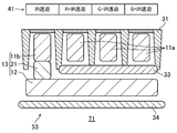
12 深層受光部
13 第2の受光部
21 接続部
31 浅層水平分離部
32 深層水平分離部
33 垂直分離部
34 垂直オーバーフローバリア
41、31a カラーフィルタ
42 IRカットフィルタ
50、51、52、53 固体撮像装置
61 受光部
62 読み出し回路部
63 ドレイン部
71 半導体基板
Claims (8)
- 半導体基板上に二次元配列された複数の画素を備え、
前記複数の画素は、それぞれ、前記半導体基板の表面近傍に形成された少なくとも一つの浅層受光部と、前記浅層受光部の下方に形成された少なくとも一つの深層受光部とを備え、
前記浅層受光部の一部と、前記深層受光部とが接続されて第2の受光部を構成すると共に、他の前記浅層受光部は第1の受光部を構成し、
前記第1の受光部における過剰電荷は、前記深層受光部に排出されることを特徴とする固体撮像装置。 - 請求項1の固体撮像装置において、
前記浅層受光部と前記深層受光部との間に設けられた垂直分離部におけるポテンシャル障壁は、前記複数の浅層受光部同士の間に設けられた浅層水平分離部におけるポテンシャル障壁よりも小さいことを特徴とする固体撮像装置。 - 請求項1又は2の固体撮像装置において、
前記第2の受光部における過剰電荷は、前記第1の受光部又は前記半導体基板に排出されることを特徴とする固体撮像装置。 - 請求項3の固体撮像装置において、
前記浅層受光部と前記深層受光部との間に設けられた垂直分離部におけるポテンシャル障壁、及び、前記深層受光部の下方に設けられた垂直オーバーフローバリアにおけるポテンシャル障壁は、前記深層受光部同士の間に設けられた深層水平分離部におけるポテンシャル障壁よりも小さいことを特徴とする固体撮像装置。 - 請求項1又は2の固体撮像装置において、
前記第2の受光部における過剰電荷は、前記半導体基板に排出されることを特徴とする固体撮像装置。 - 請求項5の固体撮像装置において、
前記深層受光部の下方に設けられた垂直オーバーフローバリアにおけるポテンシャル障壁は、前記浅層受光部と前記深層受光部との間に設けられた垂直分離部におけるポテンシャル障壁、及び、前記深層受光部同士の間に設けられた深層水平分離部におけるポテンシャル障壁よりも小さいことを特徴とする固体撮像装置。 - 請求項1~6のいずれか1つにおいて、
前記複数の画素は、それぞれ、前記第1の受光部から信号を転送するための第1の転送ゲートを更に備え、
前記第2の受光部を用いて撮像する際に、前記第1の転送ゲートを開放し、前記第1の受光部から前記第1の転送ゲートを通じて電荷を排出することを特徴とする固体撮像装置。 - 請求項1~7のいずれか1つにおいて、
前記複数の画素は、それぞれ、前記第2の受光部から信号を転送するための第2の転送ゲートを更に備え、
前記第1の受光部を用いて撮像する際に、前記第2の転送ゲートを開放し、前記第2の受光部から前記第2の転送ゲートを通じて電荷を排出することを特徴とする固体撮像装置。
Priority Applications (3)
| Application Number | Priority Date | Filing Date | Title |
|---|---|---|---|
| JP2017561532A JP6814748B2 (ja) | 2016-01-15 | 2016-11-25 | 固体撮像装置 |
| EP16885039.4A EP3404714B1 (en) | 2016-01-15 | 2016-11-25 | Solid-state image capture device |
| US16/033,478 US11289618B2 (en) | 2016-01-15 | 2018-07-12 | Solid-state imaging device |
Applications Claiming Priority (2)
| Application Number | Priority Date | Filing Date | Title |
|---|---|---|---|
| JP2016005977 | 2016-01-15 | ||
| JP2016-005977 | 2016-01-15 |
Related Child Applications (1)
| Application Number | Title | Priority Date | Filing Date |
|---|---|---|---|
| US16/033,478 Continuation US11289618B2 (en) | 2016-01-15 | 2018-07-12 | Solid-state imaging device |
Publications (1)
| Publication Number | Publication Date |
|---|---|
| WO2017122436A1 true WO2017122436A1 (ja) | 2017-07-20 |
Family
ID=59311164
Family Applications (1)
| Application Number | Title | Priority Date | Filing Date |
|---|---|---|---|
| PCT/JP2016/085074 WO2017122436A1 (ja) | 2016-01-15 | 2016-11-25 | 固体撮像装置 |
Country Status (4)
| Country | Link |
|---|---|
| US (1) | US11289618B2 (ja) |
| EP (1) | EP3404714B1 (ja) |
| JP (1) | JP6814748B2 (ja) |
| WO (1) | WO2017122436A1 (ja) |
Cited By (2)
| Publication number | Priority date | Publication date | Assignee | Title |
|---|---|---|---|---|
| WO2019180898A1 (ja) * | 2018-03-23 | 2019-09-26 | パナソニックIpマネジメント株式会社 | 固体撮像素子 |
| JP2020065026A (ja) * | 2018-10-19 | 2020-04-23 | キヤノン株式会社 | 光電変換装置 |
Families Citing this family (1)
| Publication number | Priority date | Publication date | Assignee | Title |
|---|---|---|---|---|
| WO2024086959A1 (en) * | 2022-10-24 | 2024-05-02 | Huawei Technologies Co., Ltd. | Stacked sensor for simultaneouly detecting visible light and infrared light |
Citations (10)
| Publication number | Priority date | Publication date | Assignee | Title |
|---|---|---|---|---|
| JPH0774340A (ja) * | 1993-09-01 | 1995-03-17 | Toshiba Corp | 固体撮像装置 |
| JP2001053264A (ja) * | 1999-08-09 | 2001-02-23 | Sony Corp | 固体撮像素子 |
| JP2006041866A (ja) * | 2004-07-27 | 2006-02-09 | Sony Corp | 固体撮像装置 |
| JP2008091781A (ja) * | 2006-10-04 | 2008-04-17 | Toshiba Corp | 増幅型固体撮像素子 |
| JP2008147471A (ja) * | 2006-12-12 | 2008-06-26 | Matsushita Electric Ind Co Ltd | 固体撮像装置 |
| JP2009272620A (ja) | 2008-05-09 | 2009-11-19 | Samsung Electronics Co Ltd | 積層型イメージセンサー |
| WO2010004683A1 (ja) * | 2008-07-11 | 2010-01-14 | パナソニック株式会社 | 固体撮像装置 |
| JP2010040840A (ja) * | 2008-08-06 | 2010-02-18 | Toshiba Corp | 固体撮像デバイス及びその製造方法 |
| WO2015037547A1 (ja) * | 2013-09-10 | 2015-03-19 | Sekine Hirokazu | 固体撮像装置 |
| US20160027837A1 (en) * | 2014-07-25 | 2016-01-28 | Omnivision Technologies, Inc. | Visible and infrared image sensor |
Family Cites Families (5)
| Publication number | Priority date | Publication date | Assignee | Title |
|---|---|---|---|---|
| US7755123B2 (en) * | 2007-08-24 | 2010-07-13 | Aptina Imaging Corporation | Apparatus, system, and method providing backside illuminated imaging device |
| JP5029624B2 (ja) * | 2009-01-15 | 2012-09-19 | ソニー株式会社 | 固体撮像装置及び電子機器 |
| US8492865B2 (en) * | 2009-09-24 | 2013-07-23 | Omnivision Technologies, Inc. | Image sensor with contact dummy pixels |
| JP2012124299A (ja) * | 2010-12-08 | 2012-06-28 | Toshiba Corp | 裏面照射型固体撮像装置及びその製造方法 |
| JP2013016729A (ja) * | 2011-07-06 | 2013-01-24 | Sony Corp | 固体撮像素子および電子機器 |
-
2016
- 2016-11-25 EP EP16885039.4A patent/EP3404714B1/en active Active
- 2016-11-25 JP JP2017561532A patent/JP6814748B2/ja active Active
- 2016-11-25 WO PCT/JP2016/085074 patent/WO2017122436A1/ja active Application Filing
-
2018
- 2018-07-12 US US16/033,478 patent/US11289618B2/en active Active
Patent Citations (10)
| Publication number | Priority date | Publication date | Assignee | Title |
|---|---|---|---|---|
| JPH0774340A (ja) * | 1993-09-01 | 1995-03-17 | Toshiba Corp | 固体撮像装置 |
| JP2001053264A (ja) * | 1999-08-09 | 2001-02-23 | Sony Corp | 固体撮像素子 |
| JP2006041866A (ja) * | 2004-07-27 | 2006-02-09 | Sony Corp | 固体撮像装置 |
| JP2008091781A (ja) * | 2006-10-04 | 2008-04-17 | Toshiba Corp | 増幅型固体撮像素子 |
| JP2008147471A (ja) * | 2006-12-12 | 2008-06-26 | Matsushita Electric Ind Co Ltd | 固体撮像装置 |
| JP2009272620A (ja) | 2008-05-09 | 2009-11-19 | Samsung Electronics Co Ltd | 積層型イメージセンサー |
| WO2010004683A1 (ja) * | 2008-07-11 | 2010-01-14 | パナソニック株式会社 | 固体撮像装置 |
| JP2010040840A (ja) * | 2008-08-06 | 2010-02-18 | Toshiba Corp | 固体撮像デバイス及びその製造方法 |
| WO2015037547A1 (ja) * | 2013-09-10 | 2015-03-19 | Sekine Hirokazu | 固体撮像装置 |
| US20160027837A1 (en) * | 2014-07-25 | 2016-01-28 | Omnivision Technologies, Inc. | Visible and infrared image sensor |
Non-Patent Citations (1)
| Title |
|---|
| See also references of EP3404714A4 |
Cited By (3)
| Publication number | Priority date | Publication date | Assignee | Title |
|---|---|---|---|---|
| WO2019180898A1 (ja) * | 2018-03-23 | 2019-09-26 | パナソニックIpマネジメント株式会社 | 固体撮像素子 |
| JP2020065026A (ja) * | 2018-10-19 | 2020-04-23 | キヤノン株式会社 | 光電変換装置 |
| JP7271127B2 (ja) | 2018-10-19 | 2023-05-11 | キヤノン株式会社 | 光電変換装置 |
Also Published As
| Publication number | Publication date |
|---|---|
| JP6814748B2 (ja) | 2021-01-20 |
| US20180323232A1 (en) | 2018-11-08 |
| EP3404714A1 (en) | 2018-11-21 |
| JPWO2017122436A1 (ja) | 2018-11-01 |
| EP3404714A4 (en) | 2018-12-12 |
| US11289618B2 (en) | 2022-03-29 |
| EP3404714B1 (en) | 2020-01-01 |
Similar Documents
| Publication | Publication Date | Title |
|---|---|---|
| US10825847B2 (en) | Solid-state imaging element | |
| KR102430114B1 (ko) | 고체 촬상 소자 및 그 제조 방법 및 전자 기기 | |
| EP1819151B1 (en) | Solid-state imaging device, method for driving solid-state imaging device and camera | |
| US8243176B2 (en) | Solid-state image sensor | |
| US9911773B2 (en) | Virtual high dynamic range large-small pixel image sensor | |
| JP4457325B2 (ja) | 固体撮像装置 | |
| US9143760B2 (en) | Solid-state imaging device | |
| EP2222077A2 (en) | Solid-state imaging device and electronic apparatus | |
| JPWO2017126326A1 (ja) | 固体撮像装置およびその駆動方法、並びに電子機器 | |
| JP5629995B2 (ja) | 撮像素子および撮像装置 | |
| JP2012033583A (ja) | 固体撮像素子及びその製造方法、並びに撮像装置 | |
| KR101661764B1 (ko) | 고체 촬상 장치, 그 제조 방법, 및 전자기기 | |
| JP2018198272A5 (ja) | ||
| KR20210032404A (ko) | 고체 촬상 장치 및 전자 기기 | |
| CN111508982A (zh) | 成像器件和成像装置 | |
| JP2012023137A (ja) | 固体撮像装置およびその製造方法 | |
| WO2016152512A1 (ja) | 固体撮像装置、及び、電子機器 | |
| US10812746B2 (en) | Solid-state imaging device and method for producing the same, and electronic apparatus | |
| US11289618B2 (en) | Solid-state imaging device | |
| JP2007288294A (ja) | 固体撮像装置およびカメラ | |
| JP2004335803A (ja) | Mos型固体撮像装置とその駆動方法 | |
| US20140285691A1 (en) | Solid state imaging device | |
| US20230047442A1 (en) | Solid-state imaging device and electronic device | |
| JP2010153603A (ja) | 固体撮像装置 | |
| US20220415944A1 (en) | Solid-state imaging device and electronic equipment |
Legal Events
| Date | Code | Title | Description |
|---|---|---|---|
| 121 | Ep: the epo has been informed by wipo that ep was designated in this application |
Ref document number: 16885039 Country of ref document: EP Kind code of ref document: A1 |
|
| ENP | Entry into the national phase |
Ref document number: 2017561532 Country of ref document: JP Kind code of ref document: A |
|
| NENP | Non-entry into the national phase |
Ref country code: DE |
|
| WWE | Wipo information: entry into national phase |
Ref document number: 2016885039 Country of ref document: EP |
|
| ENP | Entry into the national phase |
Ref document number: 2016885039 Country of ref document: EP Effective date: 20180816 |