WO2017122318A1 - 半導体装置 - Google Patents
半導体装置 Download PDFInfo
- Publication number
- WO2017122318A1 WO2017122318A1 PCT/JP2016/050957 JP2016050957W WO2017122318A1 WO 2017122318 A1 WO2017122318 A1 WO 2017122318A1 JP 2016050957 W JP2016050957 W JP 2016050957W WO 2017122318 A1 WO2017122318 A1 WO 2017122318A1
- Authority
- WO
- WIPO (PCT)
- Prior art keywords
- region
- semiconductor device
- resistance region
- trench
- high resistance
- Prior art date
- Legal status (The legal status is an assumption and is not a legal conclusion. Google has not performed a legal analysis and makes no representation as to the accuracy of the status listed.)
- Ceased
Links
Images










Classifications
-
- H—ELECTRICITY
- H10—SEMICONDUCTOR DEVICES; ELECTRIC SOLID-STATE DEVICES NOT OTHERWISE PROVIDED FOR
- H10D—INORGANIC ELECTRIC SEMICONDUCTOR DEVICES
- H10D30/00—Field-effect transistors [FET]
- H10D30/60—Insulated-gate field-effect transistors [IGFET]
- H10D30/64—Double-diffused metal-oxide semiconductor [DMOS] FETs
- H10D30/66—Vertical DMOS [VDMOS] FETs
- H10D30/668—Vertical DMOS [VDMOS] FETs having trench gate electrodes, e.g. UMOS transistors
-
- H—ELECTRICITY
- H10—SEMICONDUCTOR DEVICES; ELECTRIC SOLID-STATE DEVICES NOT OTHERWISE PROVIDED FOR
- H10D—INORGANIC ELECTRIC SEMICONDUCTOR DEVICES
- H10D30/00—Field-effect transistors [FET]
- H10D30/01—Manufacture or treatment
- H10D30/021—Manufacture or treatment of FETs having insulated gates [IGFET]
- H10D30/028—Manufacture or treatment of FETs having insulated gates [IGFET] of double-diffused metal oxide semiconductor [DMOS] FETs
- H10D30/0291—Manufacture or treatment of FETs having insulated gates [IGFET] of double-diffused metal oxide semiconductor [DMOS] FETs of vertical DMOS [VDMOS] FETs
- H10D30/0297—Manufacture or treatment of FETs having insulated gates [IGFET] of double-diffused metal oxide semiconductor [DMOS] FETs of vertical DMOS [VDMOS] FETs using recessing of the gate electrodes, e.g. to form trench gate electrodes
-
- H—ELECTRICITY
- H10—SEMICONDUCTOR DEVICES; ELECTRIC SOLID-STATE DEVICES NOT OTHERWISE PROVIDED FOR
- H10D—INORGANIC ELECTRIC SEMICONDUCTOR DEVICES
- H10D30/00—Field-effect transistors [FET]
- H10D30/60—Insulated-gate field-effect transistors [IGFET]
-
- H—ELECTRICITY
- H10—SEMICONDUCTOR DEVICES; ELECTRIC SOLID-STATE DEVICES NOT OTHERWISE PROVIDED FOR
- H10D—INORGANIC ELECTRIC SEMICONDUCTOR DEVICES
- H10D64/00—Electrodes of devices having potential barriers
- H10D64/111—Field plates
- H10D64/115—Resistive field plates, e.g. semi-insulating field plates
-
- H—ELECTRICITY
- H10—SEMICONDUCTOR DEVICES; ELECTRIC SOLID-STATE DEVICES NOT OTHERWISE PROVIDED FOR
- H10D—INORGANIC ELECTRIC SEMICONDUCTOR DEVICES
- H10D64/00—Electrodes of devices having potential barriers
- H10D64/111—Field plates
- H10D64/117—Recessed field plates, e.g. trench field plates or buried field plates
-
- H—ELECTRICITY
- H10—SEMICONDUCTOR DEVICES; ELECTRIC SOLID-STATE DEVICES NOT OTHERWISE PROVIDED FOR
- H10D—INORGANIC ELECTRIC SEMICONDUCTOR DEVICES
- H10D64/00—Electrodes of devices having potential barriers
- H10D64/20—Electrodes characterised by their shapes, relative sizes or dispositions
Definitions
- the present invention relates to a semiconductor device.
- a semiconductor device having a so-called shield gate structure includes a semiconductor substrate 910 including an n + -type drain region 912, an n ⁇ -type drift region 914, a p-type base region 916, and an n + -type source region 918, formed in the semiconductor substrate in 910, n - bottom adjacent to the type drift region 914, and, p-type base region 916 and the n - having a side wall adjacent to the type drift region 914, formed in stripes in plan view
- a shield electrode 930 located between the gate electrode 926 and the bottom of the trench 922, and extends between the gate electrode 926 and the shield electrode 930;
- the shield electrode 930 is provided in the trench 922 and located between the gate electrode 926 and the bottom of the trench 922, the gate electrode 926 to the bottom of the trench 922 is provided. Therefore, the gate-drain capacitance C GD (see FIG. 23B ) is reduced. As a result, the gate charge current amount and the gate discharge current amount are reduced, and the switching speed can be increased. Further, the distance from the corner portion of the trench 922 where the electric field concentration is likely to occur to the gate electrode 926 can be increased, and further, the electric field can be relaxed in the electrically insulating region 928, so that the withstand voltage can be increased.
- the present inventor considered using a high-resistance shield electrode (for example, a shield electrode having a higher resistance than the source electrode and the gate electrode) as the shield electrode (see FIGS. 3 and 4A).
- a high-resistance shield electrode for example, a shield electrode having a higher resistance than the source electrode and the gate electrode
- FIGS. 3 and 4A the shield electrode
- the potential change of the drain electrode can be moderated when the switch is turned off, thereby suppressing the ringing that occurs when the switch is turned off and reducing the surge voltage. (See FIG. 4B).
- the present invention has been made to solve these problems, and can suppress ringing that occurs when the switch is turned off, reduce the surge voltage, and the gate voltage V GS rises when the switch is turned off. It is an object of the present invention to provide a semiconductor device capable of suppressing malfunction (self-turn-on) that occurs due to the above and capable of reducing the problem of increased switching loss.
- a semiconductor device of the present invention includes a first conductivity type drain region, a first conductivity type drift region adjacent to the drain region, a second conductivity type base region adjacent to the drift region, and the base
- a semiconductor substrate including a first conductivity type source region adjacent to the region; a bottom formed in the semiconductor substrate; adjacent to the drift region; and a sidewall adjacent to the base region and the drift region;
- a shield electrode located between the gate electrode and the bottom of the trench, and extending between the gate electrode and the shield electrode, and further An electrically insulating region in the trench and extending above the semiconductor substrate and extending along the side wall and the bottom of the groove to separate the shield electrode from the side wall and the bottom, and electrically connected to the source region
- the above-described high resistance region is located at both ends of the trench in plan view and is referred to as a first region having a first resistance, and the above-described low resistance region is sandwiched between the first regions. It can also be said that the second region is located at a position and has a second resistance lower than the first resistance.
- both the high resistance region and the low resistance region are made of the same semiconductor material containing impurities, and the impurity concentration of the low resistance region is higher than the impurity concentration of the high resistance region. High is preferred.
- the high resistance region and the low resistance region are made of different materials, and the electrical resistivity of the material constituting the low resistance region is the electrical resistance of the material constituting the high resistance region. Preferably it is lower than the resistivity.
- the high resistance region and the low resistance region are each made of the same material, and the cross-sectional area of the high resistance region when cut along a plane orthogonal to the longitudinal direction of the trench is It is preferable that the cross-sectional area of the low-resistance region is smaller than that obtained by cutting along a plane perpendicular to the longitudinal direction of the trench.
- both the high resistance region and the low resistance region are made of the same semiconductor material containing impurities, and the low resistance region has a higher concentration of impurities than the high resistance region. It is preferable to include a high concentration impurity region that is contained and extends along the longitudinal direction of the trench.
- both the high resistance region and the low resistance region are made of the same semiconductor material containing impurities and extend along the longitudinal direction of the trench.
- the cross-sectional area of the high-concentration impurity region of the high-resistance region when it is cut along a plane perpendicular to the longitudinal direction of the trench includes a region, and the low resistance when cut along a plane perpendicular to the longitudinal direction of the trench The area is preferably smaller than the cross-sectional area of the high-concentration impurity region.
- the shield electrodes extending adjacent to the sides of the chip as viewed in plan are all made of the high resistance region.
- the shield electrode extending adjacent to the side of the gate pad in plan view is adjacent to the side of the gate pad in plan view. It is preferable that the extending portion is made of the high resistance region.
- a contact structure for electrically connecting the shield electrode and the source electrode is provided at an end portion connected to the source electrode among both ends of the shield electrode. Preferably it is formed.
- the contact structure is preferably formed in a second low resistance region having a lower resistance than the high resistance region.
- the source electrode is electrically connected to the shield electrode at both ends of the trench when viewed in plan, and the high resistance region is the trench when viewed in plan. It is preferable that the low resistance region is located at a position sandwiched between the high resistance recording regions.
- the shield electrode As the shield electrode, the high resistance region located at the end electrically connected to the source electrode among the both ends of the trench, and the high resistance region as viewed from the source electrode. Since the shield electrode having the low resistance region located at the position of (2) is provided (see FIG. 1, FIG. 2 (a) and FIG. 2 (b)), the resistance between the drain and the source is increased by the presence of the high resistance region. be able to. For this reason, the potential change of the drain electrode at the time of switch-off can be moderated, so that the ringing generated at the time of switch-off can be suppressed (and the surge voltage can be reduced), and the occurrence of malfunction can be suppressed (see FIG. 2 (c).)
- the presence of the low resistance region can reduce the potential difference that occurs along the wiring of the shield electrode, so that it is possible to suppress the rise of V GS in the latter half of the switching period and the malfunction (FIG. 2C). Also, the switching speed can be increased due to the presence of the low resistance region (see FIG. 2C), thereby preventing an increase in switching loss.
- the potential generated at the shield electrode increases, and the depletion layer in the drift region extends through Cds. It is suppressed.
- the switching operation of the MOSFET gradually shifts from the end electrically connected to the source electrode to the center of both ends of the trench, so that the end electrically connected to the source electrode of both ends of the trench.
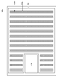
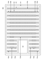
- FIG. 1 is a plan view illustrating a semiconductor device 100 according to a first embodiment.
- 1 is a diagram for explaining a semiconductor device 100 according to a first embodiment.
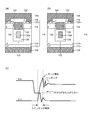
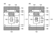
- 2A is a cross-sectional view of a main part (a region including the high resistance region 130a) of the semiconductor device 100
- FIG. 2B is a cross-sectional view of a main part (a region including the low resistance region 130b) of the semiconductor device 100.
- FIG. 2C shows a response waveform when the semiconductor device 100 is switched off.
- 7 is a plan view for explaining a semiconductor device 100a according to a comparative example 1.
- FIG. FIG. 10 is a diagram for explaining a semiconductor device 100a according to Comparative Example 1.
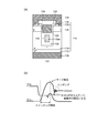
- FIG. 4A is a cross-sectional view of the main part of the semiconductor device 100a
- FIG. 4B is a diagram showing a response waveform when the semiconductor device 100a is switched off.
- 10 is a plan view for explaining a semiconductor device 100b according to Comparative Example 2.
- FIG. 10 is a diagram for explaining a semiconductor device 100b according to Comparative Example 2.
- 6A is a cross-sectional view of a main part of the semiconductor device 100b
- FIG. 6B is a diagram illustrating a response waveform when the semiconductor device 100b is switched off.
- FIG. 3 is a diagram for explaining the operation and effect of the semiconductor device 100 according to the first embodiment.
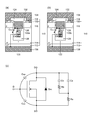
- FIG. 7A is a diagram in which parasitic resistance and parasitic capacitance are added to a cross-sectional view of a main part (a region including the high resistance region 130a) of the semiconductor device 100
- FIG. FIG. 7C is an equivalent circuit diagram of the semiconductor device 100
- FIG. 7C is a diagram in which parasitic resistance and parasitic capacitance are added to the cross-sectional view.
- 6 is a view for explaining a method of manufacturing the semiconductor device 100 according to the first embodiment.
- FIG. FIG. 8A to FIG. 8D are process diagrams. 6 is a view for explaining a method of manufacturing the semiconductor device 100 according to the first embodiment.
- FIG. FIG. 9A to FIG. 9D are process diagrams.
- FIG. 6 is a view for explaining a method of manufacturing the semiconductor device 100 according to the first embodiment.
- FIG. 10A to FIG. 10D are process diagrams. 6 is a view for explaining a method of manufacturing the semiconductor device 100 according to the first embodiment.
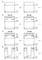
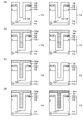
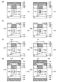
- FIG. FIGS. 11A to 11D are process diagrams. 8 to 11 and FIGS. 15, 18 and 19 to be described later, the drawings in the left column are process diagrams as seen from the cross section of the main part (region including the high resistance region 130a) of the semiconductor device. These drawings are process diagrams as seen from the cross section of the main part (region including the low resistance region 130b) of the semiconductor device.
- FIG. 6 is a main-portion cross-sectional view of a semiconductor device according to a second embodiment.
- FIG. 12A is a cross-sectional view of a main part (a region including the high resistance region 130a) of the semiconductor device
- FIG. 12B is a cross-sectional view of a main part (a region including the low resistance region 130b) of the semiconductor device
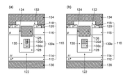
- FIG. 6 is a cross-sectional view of main parts of a semiconductor device 102 according to a third embodiment.
- 13A is a cross-sectional view of a main part (a region including the high resistance region 130a) of the semiconductor device 102
- FIG. 13B is a cross-sectional view of a main part (a region including the low resistance region 130b) of the semiconductor device 102. is there.
- FIG. 6 is a plan view for explaining a semiconductor device 102 according to a third embodiment.
- FIG. 10 is a view for explaining a method for manufacturing the semiconductor device 102 according to the third embodiment.
- FIGS. 15A to 15D are process diagrams. In FIG. 15, the illustration of steps similar to those shown in FIGS. 8 to 11 is omitted.
- FIG. 6 is a cross-sectional view of a main part of a semiconductor device according to a fourth embodiment.
- 16A is a cross-sectional view of a main part (a region including the high resistance region 130a) of the semiconductor device
- FIG. 16B is a cross-sectional view of a main part (a region including the low resistance region 130b) of the semiconductor device.
- FIG. 10 is a cross-sectional view of main parts of a semiconductor device according to a fifth embodiment.
- FIG. 17A is a cross-sectional view of a main part (a region including the high resistance region 130a) of the semiconductor device
- FIG. 17B is a cross-sectional view of a main part (a region including the low resistance region 130b) of the semiconductor device.
- FIG. 10 is a view for explaining a method for manufacturing the semiconductor device according to the fourth embodiment.
- FIG. 18A to FIG. 18D are process diagrams. In FIG. 18, illustration of the same steps as those shown in FIGS. 8 to 11 is omitted.
- FIG. 10 is a view for explaining a method for manufacturing the semiconductor device according to the fifth embodiment.
- 19A to 19D are process diagrams. In FIG. 19, illustration of the same steps as those shown in FIGS. 8 to 11 is omitted.
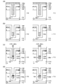
- FIG. 20A is a plan view showing an end portion of the shield electrode 130 in the semiconductor device 100 according to the first embodiment
- FIG. 20B shows an end portion of the shield electrode 130 in the semiconductor device according to the second embodiment
- FIG. 20C is a plan view showing an end portion of the shield electrode 130 in the semiconductor device 102 according to the third embodiment
- FIG. 20D is a plan view showing the shield electrode 130 in the semiconductor device according to the fourth embodiment
- FIG. 20E is a plan view showing an end portion of the shield electrode 130 in the semiconductor device 100 according to the fifth embodiment.
- FIG. 20F is a plan view showing an end portion of the shield electrode 130 in the modification of the semiconductor device 100 according to the first embodiment.
- FIG. 20A is a plan view showing an end portion of the shield electrode 130 in the semiconductor device 100 according to the first embodiment
- FIG. 20B shows an end portion of the shield electrode 130 in the semiconductor device according to the second embodiment
- FIG. 20C is a plan view showing an end portion of the shield electrode 130 in the semiconductor device 102 according
- FIG. 20G is a plan view in the modification of the semiconductor device according to the second embodiment.
- FIG. 20H is a plan view showing an end portion of the shield electrode 130 in a modification of the semiconductor device 102 according to the third embodiment
- FIG. 20I is a plan view showing the end portion of the shield electrode 130.
- FIG. FIG. 20J is a plan view illustrating an end portion of a shield electrode 130 in a modification of the semiconductor device according to the fourth embodiment
- FIG. 20J illustrates an end portion of the shield electrode 130 in a modification of the semiconductor device 100 according to the fifth embodiment. It is a top view.
- FIG. 10 is a plan view for explaining a semiconductor device 105 according to a sixth embodiment.
- FIG. 10 is a plan view for explaining a semiconductor device 105 according to a sixth embodiment.
- FIG. 10 is a plan view for explaining a semiconductor device 106 according to a seventh embodiment. It is a figure shown in order to demonstrate the conventional semiconductor device 900.
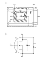
- FIG. 23A is a diagram in which parasitic resistance and parasitic capacitance are added to the cross-sectional view of the semiconductor device 900
- FIG. 23B is an equivalent circuit diagram of the semiconductor device 900.
- the semiconductor device 100 includes an n + -type drain region (first conductivity type drain region) 112, an n + -type, as shown in FIGS. 1, 2A, and 2B.
- the shield electrode 130 is located at a position sandwiched between the high resistance region 130a located at both ends of the trench 122 and the high resistance region 130a when seen in a plan view. It has a low resistance region 130b. Both the high resistance region 130a and the low resistance region 130b are made of the same semiconductor material containing impurities, and the impurity concentration of the low resistance region 130b is higher than the impurity concentration of the high resistance region 130a.
- the shield electrodes extending adjacent to the sides of the chip as viewed in plan are all made of the high resistance region 130a.
- the shield electrode extending adjacent to the side of the gate pad 138 as viewed in a plane has a high resistance at the portion extending adjacent to the side of the gate pad 138 as viewed in plan. It consists of area 130a.
- the thickness of the n + -type drain region 112 is 50 ⁇ m to 500 ⁇ m (eg, 350 ⁇ m), and the impurity concentration of the n + -type drain region 112 is 1 ⁇ 10 18 cm ⁇ 3 to 1 ⁇ 10 20 cm ⁇ 3 (eg, 1 ⁇ 10 19 cm ⁇ 3 ).
- the thickness of the n ⁇ type drift region 114 is 10 ⁇ m to 50 ⁇ m (for example, 15 ⁇ m), and the impurity concentration of the n ⁇ type drift region 114 is 1 ⁇ 10 14 cm ⁇ 3 to 1 ⁇ 10 17 cm ⁇ 3 (for example, 1 ⁇ 10 10). 15 cm ⁇ 3 ).
- the thickness of the p-type base region 116 is 2 ⁇ m to 10 ⁇ m (for example, 5 ⁇ m), and the impurity concentration of the p-type base region 116 is 1 ⁇ 10 16 cm ⁇ 3 to 1 ⁇ 10 18 cm ⁇ 3 (for example, 1 ⁇ 10 17 cm). -3 ).
- the depth of the trench 122 is 4 ⁇ m to 20 ⁇ m (for example, 12 ⁇ m), and the pitch of the trench 122 is 3 ⁇ m to 15 ⁇ m (for example, 10 ⁇ m).
- the gate insulating film 124 is made of, for example, a silicon dioxide film formed by a thermal oxidation method, and the thickness of the gate insulating film 124 is 20 nm to 200 nm (for example, 100 nm).
- the gate electrode 126 is made of, for example, low-resistance polysilicon formed by CVD, and the thickness of the gate electrode 126 is 2 ⁇ m to 10 ⁇ m (for example, 5 ⁇ m).
- the shield electrode 130 is disposed in the trench 122 and is positioned between the gate electrode 126 and the bottom of the trench 122.
- the high resistance region 130a is made of, for example, high resistance polysilicon formed by a CVD method, and the thickness of the high resistance region 130a is 1 ⁇ m to 4 ⁇ m (for example, 3 ⁇ m).
- the low resistance region 130b is made of, for example, low resistance polysilicon formed by a CVD method, and the thickness of the low resistance region 130b is 1 ⁇ m to 4 ⁇ m (for example, 3 ⁇ m).
- the distance between the shield electrode 130 and the gate electrode 126 is 1 ⁇ m to 3 ⁇ m (for example, 2 ⁇ m), and the distance between the shield electrode 130 and the bottom of the trench 122 is 1 ⁇ m to 3 ⁇ m (for example, 2 ⁇ m).
- the distance from the side wall is 1 ⁇ m to 3 ⁇ m (for example, 2 ⁇ m).
- the depth of the n + -type source region 118 is 1 ⁇ m to 3 ⁇ m (for example, 2 ⁇ m), and the impurity concentration of the n + -type source region 118 is 1 ⁇ 10 18 cm ⁇ 3 to 1 ⁇ 10 20 cm ⁇ 3 (for example, 2 ⁇ 10 19 cm ⁇ 3 ).
- the depth of the p + -type contact region 120 is 1 ⁇ m to 3 ⁇ m (for example, 2 ⁇ m), and the impurity concentration of the p + -type contact region 120 is 1 ⁇ 10 18 cm ⁇ 3 to 1 ⁇ 10 20 cm ⁇ 3 (for example, 2 ⁇ 10 19 cm ⁇ 3 ).
- the interlayer insulating film 132 is made of, for example, a silicon dioxide film formed by a CVD method, and the thickness of the interlayer insulating film 132 is 0.5 ⁇ m to 3 ⁇ m (for example, 1 ⁇ m).
- the source electrode 134 is made of, for example, an Al film or an Al alloy film (for example, an AlSi film), and the thickness of the source electrode 134 is 1 ⁇ m to 10 ⁇ m (for example, 3 ⁇ m).
- the drain electrode 136 is a laminated film in which Ti, Ni, and Au are laminated in this order, and the thickness of the drain electrode 136 is 0.2 ⁇ m to 1.5 ⁇ m (for example, 1 ⁇ m).
- the electrical resistivity and impurity concentration of the high resistance region 130a and the low resistance region 130b are not particularly limited, but the electrical resistivity of the high resistance region 130a is that of the low resistance region 130b.
- the electric resistivity is preferably 10 times or more, and more preferably 100 times or more.
- the length (one side length) of the high resistance region 130a and the low resistance region 130b along the longitudinal direction of the trench 122 is not particularly limited, but the length of the high resistance region 130a is the length of the low resistance region 130b. It is preferably 0.2 times or less, and more preferably 0.1 times or less.
- the shield electrode 130 As the shield electrode 130, the high resistance region 130a located at both ends of the trench, and the low resistance region located at a position sandwiched between the high resistance regions 130a. Since the shield electrode 130 having 130b is provided (see FIGS. 1, 2A, and 2B), the resistance value of the resistor Ra (see FIG. 7) in the high resistance region 130a is low. And the resistance value between the drain and the source can be increased by the presence of the high resistance region 130a.
- the resistance value of the resistor Rb (see FIG. 7) in the low resistance region 130b is lower than the resistance value of the resistor Ra (see FIG. 7) in the high resistance region 130a.
- the potential difference generated along the wiring 130 can be reduced, so that a malfunction (self-turn-on) caused by the rise of V GS in the latter half of the switching period can be suppressed (see FIG. 2C).
- the presence of the low resistance region 130b can increase the switching speed (see FIG. 2C), thereby preventing an increase in switching loss.
- the potential generated in the shield electrode 130 is increased, and the depletion layer extension of the n ⁇ type drift region 114 is suppressed through Cds.
- the switching operation of the MOSFET gradually moves from the both ends of the trench 122 to the center, the depletion layer extension at the both ends of the trench 122 is suppressed, so that an adverse effect due to an external surge voltage can be reduced.
- the shield electrodes 130 extending adjacent to the sides of the chip in plan view are all formed of the high resistance region 130a.
- the potential generated in the shield electrode 130 is further increased, and the depletion layer extension of the n ⁇ -type drift region 114 is further suppressed through Cds. For this reason, it is possible to reduce adverse effects due to a surge voltage from the outside of the chip.
- the shield electrode 130 extending adjacent to the side of the gate pad 138 when viewed in plan is the gate pad 138 when viewed in plan. Since the portion extending adjacent to the side of the first electrode is formed of the high resistance region 130a, the potential generated in the shield electrode 130 is further increased in the shield electrode, and the n ⁇ type drift region 114 is depleted via Cds. Layer elongation is further suppressed. For this reason, it is possible to reduce adverse effects due to the surge voltage from the gate pad 138.
- both the high resistance region 130a and the low resistance region 130b are made of the same semiconductor material containing impurities, and the impurity concentration of the low resistance region 130b is high. Since the shield electrode higher than the impurity concentration of the resistance region 130a is provided, the electrical resistivity of the high resistance region 130a and the low resistance region 130b can be set to a desired value relatively easily by setting the impurity doping amount to an appropriate value. Can be set to a value.
- the semiconductor device 100 according to the first embodiment can be manufactured by a manufacturing method (a manufacturing method of a semiconductor device according to the first embodiment) having the following manufacturing process.
- an n + type drain region 112 As shown in FIGS. 8A to 8C, an n + type drain region 112, an n ⁇ type drift region 114 adjacent to the n + type drain region 112, and an n ⁇ type drift
- a semiconductor substrate 110 including a p-type base region 116 adjacent to the region 114, an n + -type source region 118 adjacent to the p-type base region 116 and a p + -type contact region 120 is prepared.
- a mask M3 is formed on the surface of the semiconductor substrate 110, and the n ⁇ type drift region 114 is formed from the surface of the p-type base region 116 using the mask M3 as a mask.
- the trench 122 is formed to reach The depth of the trench 122 is, for example, 12 ⁇ m.
- a silicon oxide film 128 ′ is formed on the inner surface of the trench 122 and the surface of the semiconductor substrate 110 by a thermal oxidation method. Are the bottom and side walls of the electrically insulating region 128.
- the silicon oxide film 128 ′ at the bottom is formed thick by CVD, and then the silicon oxide film 128 ′ at the sidewall is formed by thermal oxidation. It is good.
- a high resistance polysilicon film 130a ′ is formed on the inside of the trench 122 and the surface of the semiconductor substrate 110 by the CVD method.
- the high-resistance polysilicon film 130a ′ is etched only in the region where the low-resistance region 130b is formed, and the high-resistance polysilicon film 130a ′ is removed.
- the high-resistance polysilicon film 130a ′ is formed only in the region where the high-resistance region 130a is formed inside the trench 122.
- a low resistance polysilicon film 130b ′ is formed in the trench 122 and on the surface of the semiconductor substrate 110 only by the CVD method in the region where the low resistance region 130b is to be formed.
- the high resistance polysilicon film 130a ′ and the low resistance polysilicon film 130b ′ are etched back, and the high resistance polysilicon film 130a ′ and the low resistance polysilicon film 130b ′ having a predetermined thickness are left.
- the silicon film 130a ′ and the low resistance polysilicon film 130b ′ are removed.
- the high resistance region 130a and the low resistance region 130b are formed inside the trench 122, and the shield electrode 130 having the high resistance region 130a and the low resistance region 130b is formed as a whole (see FIG. 10A).
- the shield electrode 130 is formed so that a part or all of the shield electrode 130 is positioned deeper than the bottom of the p-type base region 116.
- Second Electrical Insulating Region Formation Step Thereafter, a silicon oxide film having a predetermined thickness is formed on the high resistance region 130a and the low resistance region 130b inside the trench 122 by the CVD method, and this is electrically insulated region. It is set as the top of 128 (refer FIG.10 (b)).
- FIG. 10C the silicon oxide film 128 ′ formed at the site where the gate insulating film 124 is formed is removed by wet etching.
- FIG. 10D a silicon oxide film 124 ′ is formed on the surface of the semiconductor substrate 110 and a portion where the gate insulating film 124 is formed on the inner surface of the trench 122 by a thermal oxidation method.
- a gate insulating film 124 is used.
- a low resistance polysilicon film 126 ′ is formed from the surface side of the semiconductor substrate 110 so as to fill the trench 122.
- the low-resistance polysilicon film 126 ′ is etched back, and the upper low-resistance polysilicon film is left in a state where the low-resistance polysilicon film 126 ′ is left only in the trench 122. 126 'is removed.
- a final gate electrode 126 is formed on the inner peripheral surface of the trench 122.
- a source electrode 134 is formed so as to cover the semiconductor substrate 110 and the interlayer insulating film 132, and is formed on the surface of the n + -type drain region 112.
- a drain electrode 136 is formed.
- the semiconductor device 100 according to the first embodiment can be manufactured.
- the semiconductor device according to the second embodiment basically has the same configuration as the semiconductor device 100 according to the first embodiment, but the configuration of the shield electrode 130 is different from that of the semiconductor device 100 according to the first embodiment. That is, as shown in FIG. 12, in the semiconductor device according to the second embodiment, as the shield electrode 130, the high resistance region 130a and the low resistance region 130b are made of different materials, and the electric resistance of the material constituting the low resistance region 130b. A shield electrode 130 having a rate lower than the electrical resistivity of the material constituting the high resistance region 130a is provided.
- high resistance polysilicon formed by a CVD method As a material constituting the high resistance region 130a, for example, high resistance polysilicon formed by a CVD method can be used.
- a refractory metal for example, W, Mo, Ta, Nb, etc.
- other metal for example, Cu, etc.
- the configuration of the shield electrode 130 is different from that of the semiconductor device 100 according to the first embodiment. Since the shield electrode having the high resistance region 130a located and the low resistance region 130b located between the high resistance regions 130a is provided, the ringing and the like are performed as in the semiconductor device 100 according to the first embodiment. It is possible to suppress surge voltage, suppress malfunction, prevent increase in switching loss, and reduce adverse effects due to external surge voltage.
- the electrical resistivity of the high resistance region 130a and the low resistance region 130b is selected from a wide range by appropriately selecting materials for the high resistance region 130a and the low resistance region 130b. be able to.
- the semiconductor device 102 according to the third embodiment basically has the same configuration as the semiconductor device 100 according to the first embodiment, but the configuration of the shield electrode 130 is different from that of the semiconductor device 100 according to the first embodiment. That is, as shown in FIGS. 13 and 14, in the semiconductor device 102 according to the third embodiment, as the shield electrode 130, the high resistance region 130 a and the low resistance region 130 b are each made of the same material, and are arranged in the longitudinal direction of the trench 122.
- the shield electrode 130 has a smaller cross-sectional area of the high resistance region 130a when cut along a plane perpendicular to the cross section of the low resistance region 130b when cut along a plane perpendicular to the longitudinal direction of the trench 122.
- the semiconductor device 102 according to the third embodiment differs from the semiconductor device 100 according to the first embodiment in the configuration of the shield electrode 130, but the shield electrode 130 has both ends of the trench 122 as viewed in plan. Since the shield electrode having the high resistance region 130a located in the region and the low resistance region 130b located between the high resistance region 130a is provided, the ringing is performed as in the case of the semiconductor device 100 according to the first embodiment. In addition, suppression of surge voltage, suppression of malfunction, prevention of increase in switching loss, and reduction of adverse effects due to external surge voltage can be achieved.
- the thickness of the side wall portion of the electrically insulating region 128 formed in the trench 122 is divided into a region where the high resistance region 130a is formed and a low resistance region 130b.
- the area to be formed is changed (see FIGS. 15A and 15B), and the high resistance area 130a and the low resistance area 130b are formed without changing the impurity concentration (FIG. 15C).
- the semiconductor device can be manufactured by the same method as that of the semiconductor device according to the first embodiment except for (see FIG. 15D).
- the semiconductor device according to the fourth embodiment basically has the same configuration as that of the semiconductor device 100 according to the first embodiment, but the configuration of the shield electrode is different from that of the semiconductor device 100 according to the first embodiment. That is, as shown in FIG. 16, in the semiconductor device according to the fourth embodiment, as the shield electrode 130, both the high resistance region 130a and the low resistance region 130b are made of the same semiconductor material containing impurities, and the low resistance region 130b
- the shield electrode includes a high-concentration impurity region 130 d that contains a higher concentration of impurities than the high-resistance region 130 a and extends along the longitudinal direction of the trench 122. As shown in FIG. 18 (particularly FIG.
- the high resistance region 130a and the low resistance region 130b are only regions where the low resistance region 130b is formed in the polysilicon layer 130c when the ion implantation method is performed. It can be formed by forming a high concentration impurity region 130d.
- the configuration of the shield electrode 130 is different from that in the semiconductor device 100 according to the first embodiment. Since the shield electrode having the high resistance region 130a located and the low resistance region 130b located between the high resistance regions 130a is provided, the ringing and the like are performed as in the semiconductor device 100 according to the first embodiment. It is possible to suppress surge voltage, suppress malfunction, prevent increase in switching loss, and reduce adverse effects due to external surge voltage.
- the semiconductor device according to the fourth embodiment is manufactured by a method similar to the method for manufacturing the semiconductor device according to the first embodiment, except for the step of forming the high resistance region 130a and the low resistance region 130b (see FIG. 19). Can do.
- the semiconductor device according to the fifth embodiment basically has the same configuration as the semiconductor device 100 according to the first embodiment, but the configuration of the shield electrode 130 is different from that of the semiconductor device 100 according to the first embodiment. That is, as shown in FIG. 17, in the semiconductor device according to the fifth embodiment, as the shield electrode 130, both the high resistance region 130a and the low resistance region 130b are made of the same semiconductor material containing impurities, and the trench 122
- the cross-sectional area of the high-concentration impurity region 130d of the high-resistance region 130a when it is cut along a plane perpendicular to the longitudinal direction of the trench 122 includes the high-concentration impurity region 130d extending along the longitudinal direction of the trench 122.
- a shield electrode smaller than the cross-sectional area of the high-concentration impurity region 130d of the low resistance region 130b when cut along a plane orthogonal to the direction is provided. Note that, as shown in FIG. 19 (particularly FIG. 19C), the high resistance region 130a and the low resistance region 130b are formed between the high resistance region 130a and the low resistance region 130b when the ion implantation method is performed. It can be formed by changing the area of ion implantation into the silicon layer 130c and changing the cross-sectional area of the high concentration impurity region 130d.
- the configuration of the shield electrode 130 is different from that of the semiconductor device 100 according to the first embodiment. Since the shield electrode having the high resistance region 130a located and the low resistance region 130b located between the high resistance regions 130a is provided, the ringing and the like are performed as in the semiconductor device 100 according to the first embodiment. It is possible to suppress surge voltage, suppress malfunction, prevent increase in switching loss, and reduce adverse effects due to external surge voltage.
- the semiconductor device according to the fifth embodiment is manufactured by the same method as that of the semiconductor device according to the first embodiment, except for the step of forming the high resistance region 130a and the low resistance region 130b (see FIG. 19). Can do.
- the shield electrode 130 and the source electrode 134 are electrically connected to both ends of the shield electrode 130.
- a contact structure 140 may be formed for connection to the contact.
- the contact structure 140 may be formed in the second low resistance region 130e having a lower resistance than the high resistance region 130a.
- the high resistance region 130a is located in a region sandwiched between the low resistance region 130b and the second low resistance region 130e.
- the semiconductor device 105 according to the sixth embodiment basically has the same configuration as that of the semiconductor device 100 according to the first embodiment. However, the configuration of the shield electrode 130 that extends adjacent to the side of the chip in plan view. However, this is different from the case of the semiconductor device 100 according to the first embodiment. That is, as shown in FIG. 21, in the semiconductor device 105 according to the sixth embodiment, the shield electrode 130 extending adjacent to the side of the chip in plan view is the same as the shield electrode 130 at other positions.
- the low resistance region 130b is located between the high resistance regions 130a.
- the shield electrode 130 extending adjacent to the side of the gate pad 138 when viewed in a plan view also has a high resistance region like the shield electrode 130 at other positions.
- the low resistance region 130b is located at a position sandwiched by 130a.
- the semiconductor device 105 according to the sixth embodiment is different from the semiconductor device 100 according to the first embodiment in the configuration of the shield electrode 130 that extends adjacent to the side of the chip in plan view.
- the shield electrode 130 includes a shield electrode having a high resistance region 130a located at both ends of the trench 122 in a plan view and a low resistance region 130b located at a position sandwiched between the high resistance regions 130a, As in the case of the semiconductor device 100 according to the first embodiment, it is possible to suppress ringing and surge voltage, suppress malfunction, and prevent increase in switching loss.
- the semiconductor device 106 according to the seventh embodiment basically has the same configuration as the semiconductor device 100 according to the first embodiment, but the configuration of the gate finger for connecting the gate pad 138 and the gate electrode 126 is the embodiment. 1 is different from that of the semiconductor device 100 according to 1. That is, in the semiconductor device 100 according to the first embodiment, although not shown, the gate finger 142 extending from the gate pad 138 along the outer periphery of the chip is provided as a gate finger, whereas the semiconductor according to the seventh embodiment. In the device 106, as shown in FIG. 22, in addition to the gate finger 142 extending from the gate pad 138 along the outer periphery of the chip as the gate finger, the gate pad 138 extends through the center of the chip. The second gate finger 144 is provided. Along with this, the trench 122 is divided by the second gate finger 144.
- the semiconductor device 106 according to the seventh embodiment is different from the semiconductor device 100 according to the first embodiment in the configuration of the gate finger, but the shield electrode 130 is formed at both ends of the trench 122 in plan view. Since the shield electrode having the high resistance region 130a located and the low resistance region 130b located between the high resistance regions 130a is provided, the ringing and the like are performed as in the semiconductor device 100 according to the first embodiment. It is possible to suppress surge voltage, suppress malfunction, prevent increase in switching loss, and reduce adverse effects due to external surge voltage.
- the semiconductor device 106 according to the seventh embodiment there is also an effect that the adverse effect due to the surge voltage from the second gate finger 144 can be reduced.
- high resistance polysilicon formed by the CVD method is used as the high resistance region 130a
- low resistance polysilicon formed by, for example, the CVD method is used as the low resistance region 130b.
- the present invention is not limited to this. You may use materials other than these.
- high resistance polysilicon formed by a CVD method is used as the high resistance region 130a, and a refractory metal (for example, W, Mo, Ta, Nb, etc.) is used as the low resistance region 130b. .) And other metals (for example, Cu, etc.) are used, but the present invention is not limited to this. You may use materials other than these.
- the power MOSFET is described as an example of the semiconductor device 100.
- the present invention is not limited to this.
- the present invention can be variously applied to devices other than the power MOSFET without departing from the spirit of the present invention.
- the semiconductor device 100 according to the first embodiment can be manufactured by a method different from the method described in the first embodiment.
- the n + type source region 118 and the p + type contact region 120 may be formed after the shield electrode 130 and the gate electrode 126 are formed. Further, for example, after forming the shield electrode 130 and the gate electrode 126, the n + -type source region 118, the p-type base region 116, and the p + -type contact region 120 may be formed.
- the source electrode is electrically connected to the shield electrode at both ends of the trench when viewed in plan, and the high resistance region is positioned at both ends of the trench when viewed in plan.
- the low resistance region is located at a position sandwiched between the high resistance recording regions, the present invention is not limited to this.
- the source electrode is electrically connected to the shield electrode at one of both ends of the trench when viewed in plan, and the high resistance region is electrically connected to the source electrode at both ends of the trench when viewed in plan.
- the low resistance region may be located at a position ahead of the high resistance region when viewed from the source electrode.
Landscapes
- Electrodes Of Semiconductors (AREA)
- Semiconductor Integrated Circuits (AREA)
Abstract
トレンチ122内にゲート絶縁膜124を介して配設されたゲート電極126と、ゲート電極126とトレンチ122の底との間に位置するシールド電極130と、ゲート電極126とシールド電極130との間に拡がり、さらに、トレンチ122の側壁及び底に沿って拡がって側壁及び底からシールド電極130を離隔させる電気的絶縁領域128と、n+型ソース領域118に電気的に接続されるとともに平面的に見てトレンチ122の両端部においてシールド電極130に電気的に接続されたソース電極134とを備え、シールド電極130は、平面的に見てトレンチ122の両端部に位置する高抵抗領域130a、及び、高抵抗領域130aに挟まれた位置に位置する低抵抗領域130bを有する半導体装置100。リンギング及びサージ電圧の抑制、誤動作の抑制、スイッチング損失の増加防止、並びに、外部からのサージ電圧による悪影響の軽減が可能となる。
Description
本発明は、半導体装置に関する。
従来より、いわゆるシールドゲート構造を有する半導体装置が知られている(例えば、特許文献1参照。)。従来の半導体装置900は、図23(a)に示すように、n+型ドレイン領域912、n-型ドリフト領域914、p型ベース領域916及びn+型ソース領域918を含む半導体基体910と、半導体基体910内に形成され、n-型ドリフト領域914に隣接した底、及び、p型ベース領域916及びn-型ドリフト領域914に隣接した側壁を有し、平面的に見てストライプ状に形成されたトレンチ922と、トレンチ922内に配設され、かつ、側壁の部分でゲート絶縁膜924を介してp型ベース領域916と対向するゲート電極926と、トレンチ922内に配設され、かつ、ゲート電極926とトレンチ922の底との間に位置するシールド電極930と、ゲート電極926とシールド電極930との間に拡がり、さらに、トレンチ922の側壁及び底に沿って拡がって側壁及び底からシールド電極930を離隔させる、トレンチ922内における電気的絶縁領域928と、半導体基体910の上方に形成され、n+型ソース領域918とシールド電極930とに電気的に接続されたソース電極934と、n+型ドレイン領域912に隣接して形成されたドレイン電極936とを備える。
従来の半導体装置900によれば、トレンチ922内に配設され、かつ、ゲート電極926とトレンチ922の底との間に位置するシールド電極930を備えることから、ゲート電極926からトレンチ922の底までの距離が長くなるため、ゲート・ドレイン間容量CGD(図23(b)参照。)が低減し、その結果、ゲート充電電流量及びゲート放電電流量が低減し、スイッチング速度を速くできる。また、電界集中が起こり易いトレンチ922の角部からゲート電極926までの距離を長くでき、さらには、電気的絶縁領域928で電界を緩和することができる結果、耐圧を高くできる。
しかしながら、本発明者の研究により、従来の半導体装置900においては、スイッチオフ時にリンギングが発生したり高いサージ電圧が発生したりする場合があることが分かった。そこで、本発明者は、シールド電極として高抵抗のシールド電極(例えば、ソース電極やゲート電極よりも高抵抗のシールド電極)を用いることを考えた(図3及び図4(a)参照。)。このようにすれば、シールド電極の高い内部抵抗により、スイッチオフ時にドレイン電極の電位変化を緩やかにすることができ、もって、スイッチオフ時に発生するリンギングを抑制するとともにサージ電圧を低減することが可能となる(図4(b)参照)。
しかしながら、上記したようにシールド電極として高抵抗のシールド電極を用いると、スイッチング期間の後半において、シールド電極の配線に沿って電位差が生じるために、ゲート・ソース間の容量CGSを介してゲート電圧VGSが立ち上がってしまい、誤動作(セルフ・ターンオン)が発生し易くなるという問題(図4(b)符号A参照。)が発生する。また、スイッチング速度が遅くなることで(図4(b)参照。)、スイッチング損失が増加するという問題が発生する。
一方、シールド電極として低抵抗のシールド電極を用いた場合には(図5及び図6(a)参照。)、スイッチオフ時にドレイン電極の電位変化を緩やかにすることができないことから、リンギングを抑制するとともにサージ電圧を低減することが可能となるという効果が得られなくなる(図6(b)参照。)。
そこで、本発明は、これらの問題を解決するためになされたもので、スイッチオフ時に発生するリンギングを抑制するとともにサージ電圧を低減することが可能で、かつ、スイッチオフ時にゲート電圧VGSが立ち上がることに起因して発生する誤動作(セルフ・ターンオン)を抑制することが可能で、かつ、スイッチング損失が増加するという問題を軽減することが可能な半導体装置を提供することを目的とする。
[1]本発明の半導体装置は、第1導電型のドレイン領域、前記ドレイン領域に隣接した第1導電型のドリフト領域、前記ドリフト領域に隣接した第2導電型のベース領域、及び、前記ベース領域に隣接した第1導電型のソース領域を含む半導体基体と、前記半導体基体内に形成され、前記ドリフト領域に隣接した底、及び、前記ベース領域及び前記ドリフト領域に隣接した側壁を有し、平面的に見てストライプ状に形成されたトレンチと、前記トレンチ内に配設され、かつ、前記側壁の部分でゲート絶縁膜を介して前記ベース領域と対向するゲート電極と、前記トレンチ内に配設され、かつ、前記ゲート電極と前記トレンチの前記底との間に位置するシールド電極と、前記ゲート電極と前記シールド電極との間に拡がり、さらに、前記トレンチの前記側壁及び前記底に沿って拡がって前記側壁及び前記底から前記シールド電極を離隔させる、前記トレンチ内における電気的絶縁領域と、前記半導体基体の上方に形成され、前記ソース領域に電気的に接続されるとともに平面的に見て前記トレンチの両端部のうち少なくとも一方において前記シールド電極に電気的に接続されたソース電極と、前記ドレイン領域に隣接して形成されたドレイン電極とを備える半導体装置であって、前記シールド電極は、平面的に見て前記トレンチの両端部のうち前記ソース電極に電気的に接続された端部に位置する高抵抗領域、及び、前記ソース電極から見て前記高抵抗領域よりも先の位置に位置する低抵抗領域を有することを特徴とする。
なお、上記した高抵抗領域を、平面的に見て前記トレンチの両端部に位置し、第1の抵抗を有する第1領域と言い、上記した低抵抗領域を、前記第1領域に挟まれた位置に位置し、前記第1の抵抗よりも低い第2の抵抗を有する第2領域と言うこともできる。
[2]本発明の半導体装置においては、前記高抵抗領域及び前記低抵抗領域はともに不純物を含有する同一の半導体材料からなり、前記低抵抗領域の不純物濃度は前記高抵抗領域の不純物濃度よりも高いことが好ましい。
[3]本発明の半導体装置においては、前記高抵抗領域及び前記低抵抗領域はそれぞれ異なる材料からなり、前記低抵抗領域を構成する材料の電気抵抗率は前記高抵抗領域を構成する材料の電気抵抗率よりも低いことが好ましい。
[4]本発明の半導体装置においては、前記高抵抗領域及び前記低抵抗領域はそれぞれ同一の材料からなり、前記トレンチの長手方向に直交する平面で切断したときの前記高抵抗領域の断面積は、前記トレンチの長手方向に直交する平面で切断したときの前記低抵抗領域の断面積よりも小さいことが好ましい。
[5]本発明の半導体装置においては、前記高抵抗領域及び前記低抵抗領域は、ともに不純物を含有する同一の半導体材料からなり、前記低抵抗領域は、前記高抵抗領域より高濃度の不純物を含有するとともに前記トレンチの長手方向に沿って延在する高濃度不純物領域を含むことが好ましい。
[6]本発明の半導体装置においては、前記高抵抗領域及び前記低抵抗領域はともに、不純物を含有する同一の半導体材料からなり、かつ、前記トレンチの長手方向に沿って延在する高濃度不純物領域を含み、前記トレンチの長手方向に直交する平面で切断したときの前記高抵抗領域の前記高濃度不純物領域の断面積は、前記トレンチの長手方向に直交する平面で切断したときの前記低抵抗領域の前記高濃度不純物領域の断面積よりも小さいことが好ましい。
[7]本発明の半導体装置においては、前記シールド電極のうち、平面的に見てチップの辺に隣接して延在する前記シールド電極は、すべて前記高抵抗領域からなることが好ましい。
[8]本発明の半導体装置においては、前記シールド電極のうち、平面的に見てゲートパッドの辺に隣接して延在する前記シールド電極は、平面的に見て前記ゲートパッドの辺に隣接して延在する部分が前記高抵抗領域からなることが好ましい。
[9]本発明の半導体装置においては、前記シールド電極の両端部のうち前記ソース電極に接続された端部には、前記シールド電極と前記ソース電極とを電気的に接続するためのコンタクト構造が形成されていることが好ましい。
[10]本発明の半導体装置においては、前記コンタクト構造は、前記高抵抗領域よりも抵抗の低い第2低抵抗領域に形成されていることが好ましい。
[11]本発明の半導体装置においては、前記ソース電極は、平面的に見て前記トレンチの両端部において前記シールド電極に電気的に接続され、前記高抵抗領域は、平面的に見て前記トレンチの両端部に位置し、前記低抵抗領域は、前記高抵抗記領域に挟まれた位置に位置することが好ましい。
本発明の半導体装置によれば、シールド電極として、トレンチの両端部のうちソース電極に電気的に接続された端部に位置する高抵抗領域、及び、ソース電極から見て高抵抗領域よりも先の位置に位置する低抵抗領域を有するシールド電極を備えることから(図1、図2(a)及び図2(b)参照。)、高抵抗領域の存在によりドレイン・ソース間の抵抗を高くすることができる。このため、スイッチオフ時のドレイン電極の電位変化を緩やかにすることができ、もって、スイッチオフ時に発生するリンギングを抑制(及びサージ電圧を低減)して誤動作の発生を抑制することができる(図2(c)参照。)。
また、低抵抗領域の存在により、シールド電極の配線に沿って生じる電位差を低減することができ、もって、スイッチング期間の後半にVGSが立ち上がって誤動作につながることを抑制できる(図2(c)符号A参照。)また、低抵抗領域の存在により、スイッチング速度を高くすることができ(図2(c)参照。)、もって、スイッチング損失の増加を防止することができる。
さらにまた、トレンチの両端部のうちソース電極に電気的に接続された端部に位置する高抵抗領域の存在により、シールド電極に生じる電位が高くなり、Cdsを介してドリフト領域の空乏層伸長が抑制される。このとき、MOSFETのスイッチング動作はトレンチの両端部のうちソース電極に電気的に接続された端部から徐々に中央に移るため、トレンチの両端部のうちソース電極に電気的に接続された端部における空乏層伸長が抑制される結果、外部からのサージ電圧による悪影響を軽減できる。
以下、本発明の半導体装置について、図に示す実施形態に基づいて説明する。
[実施形態1]
1.半導体装置
実施形態1に係る半導体装置100は、図1、図2(a)及び図2(b)に示すように、n+型ドレイン領域(第1導電型のドレイン領域)112、n+型ドレイン領域112に隣接したn-型ドリフト領域(第1導電型のドリフト領域)114、n-型ドリフト領域114に隣接したp型ベース領域(第2導電型のベース領域)116、及び、p型ベース領域116に隣接したn+型ソース領域(第1導電型のソース領域)118を含む半導体基体110と、半導体基体110内に形成され、n-型ドリフト領域114に隣接した底、及び、p型ベース領域116及びn-型ドリフト領域114に隣接した側壁を有し、平面的に見てストライプ状に形成されたトレンチ122と、トレンチ122内に配設され、かつ、側壁の部分でゲート絶縁膜124を介してp型ベース領域116と対向するゲート電極126と、トレンチ122内に配設され、かつ、ゲート電極126とトレンチ122の底との間に位置するシールド電極130と、ゲート電極126とシールド電極130との間に拡がり、さらに、トレンチ122の側壁及び底に沿って拡がって側壁及び底からシールド電極130を離隔させる、トレンチ122内における電気的絶縁領域128と、半導体基体110の上方に形成され、n+型ソース領域118に電気的に接続されるとともに平面的に見てトレンチ122の両端部においてシールド電極130に電気的に接続されたソース電極134と、n+型ドレイン領域112に隣接して形成されたドレイン電極136とを備える。なお、図2(a)及び図2(b)中、符号132は層間絶縁膜132を示す。
実施形態1に係る半導体装置100は、パワーMOSFETである。
1.半導体装置
実施形態1に係る半導体装置100は、図1、図2(a)及び図2(b)に示すように、n+型ドレイン領域(第1導電型のドレイン領域)112、n+型ドレイン領域112に隣接したn-型ドリフト領域(第1導電型のドリフト領域)114、n-型ドリフト領域114に隣接したp型ベース領域(第2導電型のベース領域)116、及び、p型ベース領域116に隣接したn+型ソース領域(第1導電型のソース領域)118を含む半導体基体110と、半導体基体110内に形成され、n-型ドリフト領域114に隣接した底、及び、p型ベース領域116及びn-型ドリフト領域114に隣接した側壁を有し、平面的に見てストライプ状に形成されたトレンチ122と、トレンチ122内に配設され、かつ、側壁の部分でゲート絶縁膜124を介してp型ベース領域116と対向するゲート電極126と、トレンチ122内に配設され、かつ、ゲート電極126とトレンチ122の底との間に位置するシールド電極130と、ゲート電極126とシールド電極130との間に拡がり、さらに、トレンチ122の側壁及び底に沿って拡がって側壁及び底からシールド電極130を離隔させる、トレンチ122内における電気的絶縁領域128と、半導体基体110の上方に形成され、n+型ソース領域118に電気的に接続されるとともに平面的に見てトレンチ122の両端部においてシールド電極130に電気的に接続されたソース電極134と、n+型ドレイン領域112に隣接して形成されたドレイン電極136とを備える。なお、図2(a)及び図2(b)中、符号132は層間絶縁膜132を示す。
実施形態1に係る半導体装置100は、パワーMOSFETである。
そして、実施形態1に係る半導体装置100においては、シールド電極130は、平面的に見てトレンチ122の両端部に位置する高抵抗領域130a、及び、高抵抗領域130aに挟まれた位置に位置する低抵抗領域130bを有する。高抵抗領域130a及び低抵抗領域130bはともに不純物を含有する同一の半導体材料からなり、低抵抗領域130bの不純物濃度は高抵抗領域130aの不純物濃度よりも高い。
なお、実施形態1に係る半導体装置100においては、シールド電極130のうち、平面的に見てチップの辺に隣接して延在するシールド電極は、すべて高抵抗領域130aからなる。また、シールド電極130のうち、平面的に見てゲートパッド138の辺に隣接して延在するシールド電極は、平面的に見てゲートパッド138の辺に隣接して延在する部分が高抵抗領域130aからなる。
n+型ドレイン領域112の厚さは50μm~500μm(例えば350μm)であり、n+型ドレイン領域112の不純物濃度は1×1018cm-3~1×1020cm-3(例えば1×1019cm-3)である。n-型ドリフト領域114の厚さは10μm~50μm(例えば15μm)であり、n-型ドリフト領域114の不純物濃度は1×1014cm-3~1×1017cm-3(例えば1×1015cm-3)である。p型ベース領域116の厚さは2μm~10μm(例えば5μm)であり、p型ベース領域116の不純物濃度は1×1016cm-3~1×1018cm-3(例えば1×1017cm-3)である。
トレンチ122の深さは4μm~20μm(例えば12μm)であり、トレンチ122のピッチは3μm~15μm(例えば10μm)である。
ゲート絶縁膜124は例えば熱酸化法により形成された二酸化珪素膜からなり、ゲート絶縁膜124の厚さは20nm~200nm(例えば100nm)である。
ゲート電極126は例えばCVD法により形成された低抵抗のポリシリコンからなり、ゲート電極126の厚さは2μm~10μm(例えば5μm)である。
ゲート絶縁膜124は例えば熱酸化法により形成された二酸化珪素膜からなり、ゲート絶縁膜124の厚さは20nm~200nm(例えば100nm)である。
ゲート電極126は例えばCVD法により形成された低抵抗のポリシリコンからなり、ゲート電極126の厚さは2μm~10μm(例えば5μm)である。
シールド電極130は、上記したように、トレンチ122内に配設され、かつ、ゲート電極126とトレンチ122の底との間に位置する。高抵抗領域130aは例えばCVD法により形成された高抵抗のポリシリコンからなり、高抵抗領域130aの厚さは1μm~4μm(例えば3μm)である。低抵抗領域130bは例えばCVD法により形成された低抵抗のポリシリコンからなり、低抵抗領域130bの厚さは1μm~4μm(例えば3μm)である。
シールド電極130とゲート電極126との間隔は1μm~3μm(例えば2μm)であり、シールド電極130とトレンチ122の底との間隔は1μm~3μm(例えば2μm)であり、シールド電極130とトレンチ122の側壁との間隔は1μm~3μm(例えば2μm)である。
n+型ソース領域118の深さは1μm~3μm(例えば2μm)であり、n+型ソース領域118の不純物濃度は1×1018cm-3~1×1020cm-3(例えば2×1019cm-3)である。
p+型コンタクト領域120の深さは1μm~3μm(例えば2μm)であり、p+型コンタクト領域120の不純物濃度は1×1018cm-3~1×1020cm-3(例えば2×1019cm-3)である。
層間絶縁膜132は例えばCVD法により形成された二酸化珪素膜からなり、層間絶縁膜132の厚さは0.5μm~3μm(例えば1μm)である。
p+型コンタクト領域120の深さは1μm~3μm(例えば2μm)であり、p+型コンタクト領域120の不純物濃度は1×1018cm-3~1×1020cm-3(例えば2×1019cm-3)である。
層間絶縁膜132は例えばCVD法により形成された二酸化珪素膜からなり、層間絶縁膜132の厚さは0.5μm~3μm(例えば1μm)である。
ソース電極134は例えばAl膜又はAl合金膜(例えばAlSi膜)からなり、ソース電極134の厚さは1μm~10μm(例えば3μm)である。
ドレイン電極136はTi、Ni及びAuがこの順序で積層された積層膜からなり、ドレイン電極136の厚さは0.2μm~1.5μm(例えば1μm)である。
ドレイン電極136はTi、Ni及びAuがこの順序で積層された積層膜からなり、ドレイン電極136の厚さは0.2μm~1.5μm(例えば1μm)である。
実施形態1に係る半導体装置100において、高抵抗領域130a及び低抵抗領域130bの電気抵抗率や不純物濃度などは特に限定されるものでないが、高抵抗領域130aの電気抵抗率が低抵抗領域130bの電気抵抗率の10倍以上であることが好ましく、100倍以上であることがより一層好ましい。トレンチ122の長手方向に沿った高抵抗領域130a及び低抵抗領域130bの長さ(片側長さ)も特に限定されるものでないが、高抵抗領域130aの長さが低抵抗領域130bの長さの0.2倍以下であることが好ましく、0.1倍以下であることがより一層好ましい。
2.半導体装置の効果
実施形態1に係る半導体装置100によれば、シールド電極130として、トレンチの両端部に位置する高抵抗領域130a、及び、高抵抗領域130aに挟まれた位置に位置する低抵抗領域130bを有するシールド電極130を備えることから(図1、図2(a)及び図2(b)参照。)、高抵抗領域130aにおける抵抗Ra(図7参照。)の抵抗値が低抵抗領域130bにおける抵抗Rb(図7参照。)の抵抗値よりも高くなり、高抵抗領域130aの存在によりドレイン・ソース間の抵抗を高くすることができる。このため、スイッチオフ時のドレイン電極136の電位変化を緩やかにすることができ、もって、スイッチオフ時に発生するリンギングを抑制(及びサージ電圧を低減)して誤動作の発生を抑制することができる(図2(c)参照。)。
実施形態1に係る半導体装置100によれば、シールド電極130として、トレンチの両端部に位置する高抵抗領域130a、及び、高抵抗領域130aに挟まれた位置に位置する低抵抗領域130bを有するシールド電極130を備えることから(図1、図2(a)及び図2(b)参照。)、高抵抗領域130aにおける抵抗Ra(図7参照。)の抵抗値が低抵抗領域130bにおける抵抗Rb(図7参照。)の抵抗値よりも高くなり、高抵抗領域130aの存在によりドレイン・ソース間の抵抗を高くすることができる。このため、スイッチオフ時のドレイン電極136の電位変化を緩やかにすることができ、もって、スイッチオフ時に発生するリンギングを抑制(及びサージ電圧を低減)して誤動作の発生を抑制することができる(図2(c)参照。)。
また、低抵抗領域130bにおける抵抗Rb(図7参照。)の抵抗値が高抵抗領域130aにおける抵抗Ra(図7参照。)の抵抗値よりも低くなり、低抵抗領域130bの存在により、シールド電極130の配線に沿って生じる電位差を低減することができ、もって、スイッチング期間の後半にVGSが立ち上がることに起因して発生する誤動作(セルフ・ターンオン)を抑制できる(図2(c)符号A参照。)また、低抵抗領域130bの存在により、スイッチング速度を高くすることができ(図2(c)参照。)、もって、スイッチング損失の増加を防止することができる。
さらにまた、トレンチ122両端部に位置する高抵抗領域130aの存在により、シールド電極130に生じる電位が高くなり、Cdsを介してn-型ドリフト領域114の空乏層伸長が抑制される。このとき、MOSFETのスイッッチング動作はトレンチ122両端部から徐々に中央に移るため、トレンチ122両端部における空乏層伸長が抑制される結果、外部からのサージ電圧による悪影響を軽減できる。
また、実施形態1に係る半導体装置100によれば、シールド電極130のうち、平面的に見てチップの辺に隣接して延在するシールド電極130は、すべて高抵抗領域130aからなることから、当該シールド電極においては、シールド電極130に生じる電位がより一層高くなり、Cdsを介してn-型ドリフト領域114の空乏層伸長がより一層抑制される。このため、チップ外部からのサージ電圧による悪影響の軽減が可能となる。
また、実施形態1に係る半導体装置100によれば、シールド電極130のうち、平面的に見てゲートパッド138の辺に隣接して延在するシールド電極130は、平面的に見てゲートパッド138の辺に隣接して延在する部分が高抵抗領域130aからなることから、当該シールド電極においては、シールド電極130に生じる電位がより一層高くなり、Cdsを介してn-型ドリフト領域114の空乏層伸長がより一層抑制される。このため、ゲートパッド138からのサージ電圧による悪影響の軽減が可能となる。
また、実施形態1に係る半導体装置100によれば、シールド電極130として、高抵抗領域130a及び低抵抗領域130bがともに不純物を含有する同一の半導体材料からなり、低抵抗領域130bの不純物濃度が高抵抗領域130aの不純物濃度よりも高いシールド電極を備えることから、不純物のドープ量を適宜の値に設定することにより、高抵抗領域130a及び低抵抗領域130bの電気抵抗率を比較的容易に所望の値に設定することができる。
3.半導体装置の製造方法
実施形態1に係る半導体装置100は、以下に示す製造工程を有する製造方法(実施形態1に係る半導体装置の製造方法)により製造することができる。
実施形態1に係る半導体装置100は、以下に示す製造工程を有する製造方法(実施形態1に係る半導体装置の製造方法)により製造することができる。
(1)半導体基体準備工程
図8(a)~図8(c)に示すように、n+型ドレイン領域112、n+型ドレイン領域112に隣接したn-型ドリフト領域114、n-型ドリフト領域114に隣接したp型ベース領域116、p型ベース領域116に隣接したn+型ソース領域118及びp+型コンタクト領域120を含む半導体基体110を準備する。
図8(a)~図8(c)に示すように、n+型ドレイン領域112、n+型ドレイン領域112に隣接したn-型ドリフト領域114、n-型ドリフト領域114に隣接したp型ベース領域116、p型ベース領域116に隣接したn+型ソース領域118及びp+型コンタクト領域120を含む半導体基体110を準備する。
(2)トレンチ形成工程
その後、図8(d)に示すように、半導体基体110の表面にマスクM3を形成し、当該マスクM3をマスクとしてp型ベース領域116の表面からn-型ドリフト領域114に達するようにトレンチ122を形成する。トレンチ122の深さは例えば12μmとする。
その後、図8(d)に示すように、半導体基体110の表面にマスクM3を形成し、当該マスクM3をマスクとしてp型ベース領域116の表面からn-型ドリフト領域114に達するようにトレンチ122を形成する。トレンチ122の深さは例えば12μmとする。
(3)第1の電気的絶縁領域形成工程
その後、図9(a)に示すように、熱酸化法により、トレンチ122の内面及び半導体基体110の表面にシリコン酸化膜128’を形成し、これを電気的絶縁領域128の底部及び側壁部とする。なお、第1の電気的絶縁領域形成工程においては、CVD法により底の部分のシリコン酸化膜128’を厚く形成し、その後、熱酸化法により側壁の部分のシリコン酸化膜128’を形成することとしてもよい。
その後、図9(a)に示すように、熱酸化法により、トレンチ122の内面及び半導体基体110の表面にシリコン酸化膜128’を形成し、これを電気的絶縁領域128の底部及び側壁部とする。なお、第1の電気的絶縁領域形成工程においては、CVD法により底の部分のシリコン酸化膜128’を厚く形成し、その後、熱酸化法により側壁の部分のシリコン酸化膜128’を形成することとしてもよい。
(4)シールド電極形成工程
その後、図9(b)に示すように、CVD法により、トレンチ122の内部及び半導体基体110の表面に高抵抗ポリシリコン膜130a’を形成し、その後、図9(c)に示すように、低抵抗領域130bを形成する領域のみにおいて高抵抗ポリシリコン膜130a’のエッチングを行い、高抵抗ポリシリコン膜130a’を除去する。これにより、トレンチ122内部の高抵抗領域130aを形成する領域のみに高抵抗ポリシリコン膜130a’が形成される。
その後、図9(d)に示すように、CVD法により、低抵抗領域130bを形成する領域のみにおいてトレンチ122の内部及び半導体基体110の表面に低抵抗ポリシリコン膜130b’を形成する。
その後、図9(b)に示すように、CVD法により、トレンチ122の内部及び半導体基体110の表面に高抵抗ポリシリコン膜130a’を形成し、その後、図9(c)に示すように、低抵抗領域130bを形成する領域のみにおいて高抵抗ポリシリコン膜130a’のエッチングを行い、高抵抗ポリシリコン膜130a’を除去する。これにより、トレンチ122内部の高抵抗領域130aを形成する領域のみに高抵抗ポリシリコン膜130a’が形成される。
その後、図9(d)に示すように、CVD法により、低抵抗領域130bを形成する領域のみにおいてトレンチ122の内部及び半導体基体110の表面に低抵抗ポリシリコン膜130b’を形成する。
その後、高抵抗ポリシリコン膜130a’及び低抵抗ポリシリコン膜130b’のエッチバックを行い、所定厚さの高抵抗ポリシリコン膜130a’及び低抵抗ポリシリコン膜130b’を残した状態で高抵抗ポリシリコン膜130a’及び低抵抗ポリシリコン膜130b’を除去する。
これにより、トレンチ122内部に高抵抗領域130a及び低抵抗領域130bが形成され、全体として、高抵抗領域130a及び低抵抗領域130bを有するシールド電極130が形成される(図10(a)参照)。なお、シールド電極130は、当該シールド電極130の一部又は全部が、p型ベース領域116の底部よりも深い位置に位置するよう形成される。
これにより、トレンチ122内部に高抵抗領域130a及び低抵抗領域130bが形成され、全体として、高抵抗領域130a及び低抵抗領域130bを有するシールド電極130が形成される(図10(a)参照)。なお、シールド電極130は、当該シールド電極130の一部又は全部が、p型ベース領域116の底部よりも深い位置に位置するよう形成される。
(5)第2の電気的絶縁領域形成工程
その後、CVD法により、トレンチ122内部の高抵抗領域130a及び低抵抗領域130b上に所定厚さのシリコン酸化膜を形成し、これを電気的絶縁領域128の頂部とする(図10(b)参照。)。
その後、CVD法により、トレンチ122内部の高抵抗領域130a及び低抵抗領域130b上に所定厚さのシリコン酸化膜を形成し、これを電気的絶縁領域128の頂部とする(図10(b)参照。)。
(6)ゲート絶縁膜形成工程
その後、図10(c)に示すように、ウェットエッチングにより、ゲート絶縁膜124を形成する部位に形成されているシリコン酸化膜128’を除去する。その後、図10(d)に示すように、熱酸化法により、トレンチ122の内面におけるゲート絶縁膜124を形成する部位及び半導体基体110の表面にシリコン酸化膜124’を形成し、これを最終的なゲート絶縁膜124とする。
その後、図10(c)に示すように、ウェットエッチングにより、ゲート絶縁膜124を形成する部位に形成されているシリコン酸化膜128’を除去する。その後、図10(d)に示すように、熱酸化法により、トレンチ122の内面におけるゲート絶縁膜124を形成する部位及び半導体基体110の表面にシリコン酸化膜124’を形成し、これを最終的なゲート絶縁膜124とする。
(7)ゲート電極形成工程
その後、図11(a)に示すように、半導体基体110の表面側から、トレンチ122を埋めるように低抵抗ポリシリコン膜126’を形成する。その後、図11(b)に示すように、低抵抗ポリシリコン膜126’のエッチバックを行い、トレンチ122の内部にのみ低抵抗ポリシリコン膜126’を残した状態で上方の低抵抗ポリシリコン膜126’を除去する。これにより、トレンチ122の内周面に最終的なゲート電極126が形成される。
その後、図11(a)に示すように、半導体基体110の表面側から、トレンチ122を埋めるように低抵抗ポリシリコン膜126’を形成する。その後、図11(b)に示すように、低抵抗ポリシリコン膜126’のエッチバックを行い、トレンチ122の内部にのみ低抵抗ポリシリコン膜126’を残した状態で上方の低抵抗ポリシリコン膜126’を除去する。これにより、トレンチ122の内周面に最終的なゲート電極126が形成される。
(8)層間絶縁膜形成工程
その後、半導体基体110の表面におけるシリコン酸化膜124’を除去し、その後、半導体基体110の表面側から気相法によりPSG膜を形成し、さらにその後、ゲート電極126の上部所定部分を残してシリコンの熱酸化膜及びPSG膜をエッチングにより除去する。これにより、図11(c)に示すように、ゲート電極126の上部に層間絶縁膜132が形成される。
その後、半導体基体110の表面におけるシリコン酸化膜124’を除去し、その後、半導体基体110の表面側から気相法によりPSG膜を形成し、さらにその後、ゲート電極126の上部所定部分を残してシリコンの熱酸化膜及びPSG膜をエッチングにより除去する。これにより、図11(c)に示すように、ゲート電極126の上部に層間絶縁膜132が形成される。
(9)ソース電極及びドレイン電極形成工程
その後、図11(d)に示すように、半導体基体110及び層間絶縁膜132を覆うようにソース電極134を形成し、n+型ドレイン領域112の表面にドレイン電極136を形成する。
その後、図11(d)に示すように、半導体基体110及び層間絶縁膜132を覆うようにソース電極134を形成し、n+型ドレイン領域112の表面にドレイン電極136を形成する。
以上の工程を実施することにより、実施形態1に係る半導体装置100を製造することができる。
[実施形態2]
実施形態2に係る半導体装置は、基本的には実施形態1に係る半導体装置100と同様の構成を有するが、シールド電極130の構成が実施形態1に係る半導体装置100の場合とは異なる。すなわち、図12に示すように、実施形態2に係る半導体装置が、シールド電極130として、高抵抗領域130a及び低抵抗領域130bはそれぞれ異なる材料からなり、低抵抗領域130bを構成する材料の電気抵抗率が高抵抗領域130aを構成する材料の電気抵抗率よりも低いシールド電極130を備える。
実施形態2に係る半導体装置は、基本的には実施形態1に係る半導体装置100と同様の構成を有するが、シールド電極130の構成が実施形態1に係る半導体装置100の場合とは異なる。すなわち、図12に示すように、実施形態2に係る半導体装置が、シールド電極130として、高抵抗領域130a及び低抵抗領域130bはそれぞれ異なる材料からなり、低抵抗領域130bを構成する材料の電気抵抗率が高抵抗領域130aを構成する材料の電気抵抗率よりも低いシールド電極130を備える。
高抵抗領域130aを構成する材料としては、例えばCVD法により形成された高抵抗のポリシリコンを用いることができる。また、低抵抗領域130bとしては、高融点金属(例えば、W、Mo、Ta、Nbなど。)やその他の金属(例えば、Cuなど。)を用いることができる。
このように、実施形態2に係る半導体装置は、シールド電極130の構成が実施形態1に係る半導体装置100の場合とは異なるが、シールド電極130として、平面的に見てトレンチ122の両端部に位置する高抵抗領域130a、及び、高抵抗領域130aに挟まれた位置に位置する低抵抗領域130bを有するシールド電極を備えることから、実施形態1に係る半導体装置100の場合と同様に、リンギング及びサージ電圧の抑制、誤動作の抑制、スイッチング損失の増加防止、並びに、外部からのサージ電圧による悪影響の軽減が可能となる。
また、実施形態2に係る半導体装置によれば、高抵抗領域130a及び低抵抗領域130bの材料を適宜選択することにより、高抵抗領域130a及び低抵抗領域130bの電気抵抗率を幅広い範囲から選択することができる。
[実施形態3]
実施形態3に係る半導体装置102は、基本的には実施形態1に係る半導体装置100と同様の構成を有するが、シールド電極130の構成が実施形態1に係る半導体装置100の場合とは異なる。すなわち、図13及び図14に示すように、実施形態3に係る半導体装置102は、シールド電極130として、高抵抗領域130a及び低抵抗領域130bがそれぞれ同一の材料からなり、トレンチ122の長手方向に直交する平面で切断したときの高抵抗領域130aの断面積が、トレンチ122の長手方向に直交する平面で切断したときの低抵抗領域130bの断面積よりも小さいシールド電極130を備える。
実施形態3に係る半導体装置102は、基本的には実施形態1に係る半導体装置100と同様の構成を有するが、シールド電極130の構成が実施形態1に係る半導体装置100の場合とは異なる。すなわち、図13及び図14に示すように、実施形態3に係る半導体装置102は、シールド電極130として、高抵抗領域130a及び低抵抗領域130bがそれぞれ同一の材料からなり、トレンチ122の長手方向に直交する平面で切断したときの高抵抗領域130aの断面積が、トレンチ122の長手方向に直交する平面で切断したときの低抵抗領域130bの断面積よりも小さいシールド電極130を備える。
このように、実施形態3に係る半導体装置102は、シールド電極130の構成が実施形態1に係る半導体装置100の場合とは異なるが、シールド電極130として、平面的に見てトレンチ122の両端部に位置する高抵抗領域130a、及び、高抵抗領域130aに挟まれた位置に位置する低抵抗領域130bを有するシールド電極を備えることから、実施形態1に係る半導体装置100の場合と同様に、リンギング及びサージ電圧の抑制、誤動作の抑制、スイッチング損失の増加防止、並びに、外部からのサージ電圧による悪影響の軽減が可能となる。
実施形態3に係る半導体装置102は、図15に示すように、トレンチ122の内部に形成する電気的絶縁領域128の側壁部の厚さを高抵抗領域130aを形成する領域と低抵抗領域130bを形成する領域とで変えること(図15(a)及び図15(b)参照。)、及び、不純物濃度を変えずに高抵抗領域130a及び低抵抗領域130bを形成すること(図15(c)及び図15(d)参照。)を除いて、実施形態1に係る半導体装置の製造方法と同様の方法で製造することができる。
[実施形態4]
実施形態4に係る半導体装置は、基本的には実施形態1に係る半導体装置100と同様の構成を有するが、シールド電極の構成が実施形態1に係る半導体装置100の場合とは異なる。すなわち、図16に示すように、実施形態4に係る半導体装置は、シールド電極130として、高抵抗領域130a及び低抵抗領域130bがともに不純物を含有する同一の半導体材料からなり、低抵抗領域130bが、高抵抗領域130aより高濃度の不純物を含有するとともにトレンチ122の長手方向に沿って延在する高濃度不純物領域130dを含むシールド電極を備える。なお、高抵抗領域130a及び低抵抗領域130bは、図18(特に図18(c))に示すように、イオン注入法を実施する際にポリシリコン層130cにおける低抵抗領域130bを形成する領域のみに高濃度不純物領域130dを形成することにより形成することができる。
実施形態4に係る半導体装置は、基本的には実施形態1に係る半導体装置100と同様の構成を有するが、シールド電極の構成が実施形態1に係る半導体装置100の場合とは異なる。すなわち、図16に示すように、実施形態4に係る半導体装置は、シールド電極130として、高抵抗領域130a及び低抵抗領域130bがともに不純物を含有する同一の半導体材料からなり、低抵抗領域130bが、高抵抗領域130aより高濃度の不純物を含有するとともにトレンチ122の長手方向に沿って延在する高濃度不純物領域130dを含むシールド電極を備える。なお、高抵抗領域130a及び低抵抗領域130bは、図18(特に図18(c))に示すように、イオン注入法を実施する際にポリシリコン層130cにおける低抵抗領域130bを形成する領域のみに高濃度不純物領域130dを形成することにより形成することができる。
このように、実施形態4に係る半導体装置は、シールド電極130の構成が実施形態1に係る半導体装置100の場合とは異なるが、シールド電極130として、平面的に見てトレンチ122の両端部に位置する高抵抗領域130a、及び、高抵抗領域130aに挟まれた位置に位置する低抵抗領域130bを有するシールド電極を備えることから、実施形態1に係る半導体装置100の場合と同様に、リンギング及びサージ電圧の抑制、誤動作の抑制、スイッチング損失の増加防止、並びに、外部からのサージ電圧による悪影響の軽減が可能となる。
実施形態4に係る半導体装置は、高抵抗領域130a及び低抵抗領域130bを形成する工程(図19参照。)を除いて、実施形態1に係る半導体装置の製造方法と同様の方法で製造することができる。
[実施形態5]
実施形態5に係る半導体装置は、基本的には実施形態1に係る半導体装置100と同様の構成を有するが、シールド電極130の構成が実施形態1に係る半導体装置100の場合とは異なる。すなわち、図17に示すように、実施形態5に係る半導体装置は、シールド電極130として、高抵抗領域130a及び低抵抗領域130bがともに、不純物を含有する同一の半導体材料からなり、かつ、トレンチ122の長手方向に沿って延在する高濃度不純物領域130dを含み、トレンチ122の長手方向に直交する平面で切断したときの高抵抗領域130aの高濃度不純物領域130dの断面積が、トレンチ122の長手方向に直交する平面で切断したときの低抵抗領域130bの高濃度不純物領域130dの断面積よりも小さいシールド電極を備える。なお、高抵抗領域130a及び低抵抗領域130bは、図19(特に図19(c))に示すように、イオン注入法を実施する際に高抵抗領域130aと低抵抗領域130bとの間でポリシリコン層130cにイオン注入する面積を変えて高濃度不純物領域130dの断面積を変えることにより形成することができる。
実施形態5に係る半導体装置は、基本的には実施形態1に係る半導体装置100と同様の構成を有するが、シールド電極130の構成が実施形態1に係る半導体装置100の場合とは異なる。すなわち、図17に示すように、実施形態5に係る半導体装置は、シールド電極130として、高抵抗領域130a及び低抵抗領域130bがともに、不純物を含有する同一の半導体材料からなり、かつ、トレンチ122の長手方向に沿って延在する高濃度不純物領域130dを含み、トレンチ122の長手方向に直交する平面で切断したときの高抵抗領域130aの高濃度不純物領域130dの断面積が、トレンチ122の長手方向に直交する平面で切断したときの低抵抗領域130bの高濃度不純物領域130dの断面積よりも小さいシールド電極を備える。なお、高抵抗領域130a及び低抵抗領域130bは、図19(特に図19(c))に示すように、イオン注入法を実施する際に高抵抗領域130aと低抵抗領域130bとの間でポリシリコン層130cにイオン注入する面積を変えて高濃度不純物領域130dの断面積を変えることにより形成することができる。
このように、実施形態5に係る半導体装置は、シールド電極130の構成が実施形態1に係る半導体装置100の場合とは異なるが、シールド電極130として、平面的に見てトレンチ122の両端部に位置する高抵抗領域130a、及び、高抵抗領域130aに挟まれた位置に位置する低抵抗領域130bを有するシールド電極を備えることから、実施形態1に係る半導体装置100の場合と同様に、リンギング及びサージ電圧の抑制、誤動作の抑制、スイッチング損失の増加防止、並びに、外部からのサージ電圧による悪影響の軽減が可能となる。
実施形態5に係る半導体装置は、高抵抗領域130a及び低抵抗領域130bを形成する工程(図19参照。)を除いて、実施形態1に係る半導体装置の製造方法と同様の方法で製造することができる。
[実施形態1~5におけるコンタクト構造]
実施形態1~5係る本発明の半導体装置においては、図20(a)~図20(e)に示すように、シールド電極130の両端部には、シールド電極130とソース電極134とを電気的に接続するためのコンタクト構造140が形成されていてもよい。この場合、図20(f)~図20(j)に示すように、当該コンタクト構造140は、高抵抗領域130aよりも抵抗の低い第2低抵抗領域130eに形成されていてもよい。この場合、低抵抗領域130bと第2低抵抗領域130eとに挟まれた領域に高抵抗領域130aが位置することとなる。
実施形態1~5係る本発明の半導体装置においては、図20(a)~図20(e)に示すように、シールド電極130の両端部には、シールド電極130とソース電極134とを電気的に接続するためのコンタクト構造140が形成されていてもよい。この場合、図20(f)~図20(j)に示すように、当該コンタクト構造140は、高抵抗領域130aよりも抵抗の低い第2低抵抗領域130eに形成されていてもよい。この場合、低抵抗領域130bと第2低抵抗領域130eとに挟まれた領域に高抵抗領域130aが位置することとなる。
[実施形態6]
実施形態6に係る半導体装置105は、基本的には実施形態1に係る半導体装置100と同様の構成を有するが、平面的に見てチップの辺に隣接して延在するシールド電極130の構成が実施形態1に係る半導体装置100の場合とは異なる。すなわち、図21に示すように、実施形態6に係る半導体装置105においては、平面的に見てチップの辺に隣接して延在するシールド電極130も、そのほかの位置にあるシールド電極130と同様に、高抵抗領域130aに挟まれた位置に位置する低抵抗領域130bを有する。なお、実施形態6に係る半導体装置105においては、平面的に見てゲートパッド138の辺に隣接して延在するシールド電極130も、そのほかの位置にあるシールド電極130と同様に、高抵抗領域130aに挟まれた位置に位置する低抵抗領域130bを有する。
実施形態6に係る半導体装置105は、基本的には実施形態1に係る半導体装置100と同様の構成を有するが、平面的に見てチップの辺に隣接して延在するシールド電極130の構成が実施形態1に係る半導体装置100の場合とは異なる。すなわち、図21に示すように、実施形態6に係る半導体装置105においては、平面的に見てチップの辺に隣接して延在するシールド電極130も、そのほかの位置にあるシールド電極130と同様に、高抵抗領域130aに挟まれた位置に位置する低抵抗領域130bを有する。なお、実施形態6に係る半導体装置105においては、平面的に見てゲートパッド138の辺に隣接して延在するシールド電極130も、そのほかの位置にあるシールド電極130と同様に、高抵抗領域130aに挟まれた位置に位置する低抵抗領域130bを有する。
このように、実施形態6に係る半導体装置105は、平面的に見てチップの辺に隣接して延在するシールド電極130の構成が実施形態1に係る半導体装置100の場合とは異なるが、シールド電極130として、平面的に見てトレンチ122の両端部に位置する高抵抗領域130a、及び、高抵抗領域130aに挟まれた位置に位置する低抵抗領域130bを有するシールド電極を備えることから、実施形態1に係る半導体装置100の場合と同様に、リンギング及びサージ電圧の抑制、誤動作の抑制、並びに、スイッチング損失の増加防止が可能となる。
[実施形態7]
実施形態7に係る半導体装置106は、基本的には実施形態1に係る半導体装置100と同様の構成を有するが、ゲートパッド138とゲート電極126とを連結するためのゲートフィンガーの構成が実施形態1に係る半導体装置100の場合とは異なる。すなわち、実施形態1に係る半導体装置100においては、図示しないが、ゲートフィンガーとして、ゲートパッド138からチップ外周部に沿って延在したゲートフィンガー142を備えるのに対して、実施形態7に係る半導体装置106においては、図22に示すように、ゲートフィンガーとして、ゲートパッド138からチップ外周部に沿って延在したゲートフィンガー142に加えて、ゲートパッド138からチップ中央部を貫通するように延在した第2ゲートフィンガー144を備える。また、これにともない、トレンチ122が第2ゲートフィンガー144により分断されている。
実施形態7に係る半導体装置106は、基本的には実施形態1に係る半導体装置100と同様の構成を有するが、ゲートパッド138とゲート電極126とを連結するためのゲートフィンガーの構成が実施形態1に係る半導体装置100の場合とは異なる。すなわち、実施形態1に係る半導体装置100においては、図示しないが、ゲートフィンガーとして、ゲートパッド138からチップ外周部に沿って延在したゲートフィンガー142を備えるのに対して、実施形態7に係る半導体装置106においては、図22に示すように、ゲートフィンガーとして、ゲートパッド138からチップ外周部に沿って延在したゲートフィンガー142に加えて、ゲートパッド138からチップ中央部を貫通するように延在した第2ゲートフィンガー144を備える。また、これにともない、トレンチ122が第2ゲートフィンガー144により分断されている。
このように、実施形態7に係る半導体装置106は、ゲートフィンガーの構成が実施形態1に係る半導体装置100の場合とは異なるが、シールド電極130として、平面的に見てトレンチ122の両端部に位置する高抵抗領域130a、及び、高抵抗領域130aに挟まれた位置に位置する低抵抗領域130bを有するシールド電極を備えることから、実施形態1に係る半導体装置100の場合と同様に、リンギング及びサージ電圧の抑制、誤動作の抑制、スイッチング損失の増加防止、並びに、外部からのサージ電圧による悪影響の軽減が可能となる。
また、実施形態7に係る半導体装置106によれば、第2ゲートフィンガー144からのサージ電圧による悪影響を軽減できるという効果も得られる。
以上、本発明を上記の実施形態に基づいて説明したが、本発明は上記の実施形態に限定されるものではない。その趣旨を逸脱しない範囲において種々の態様において実施することが可能であり、例えば、次のような変形も可能である。
(1)上記実施形態1においては、高抵抗領域130aとして、例えばCVD法により形成された高抵抗のポリシリコンを用い、低抵抗領域130bとして例えばCVD法により形成された低抵抗のポリシリコンを用いたが、本発明はこれに限定されるものではない。これら以外の材料を用いてもよい。
(2)上記実施形態2においては、高抵抗領域130aとして、例えばCVD法により形成された高抵抗のポリシリコンを用い、低抵抗領域130bとして高融点金属(例えば、W、Mo、Ta、Nbなど。)やその他の金属(例えば、Cuなど。)を用いたが、本発明はこれに限定されるものではない。これら以外の材料を用いてもよい。
(3)上記実施形態1においては、半導体装置100として、パワーMOSFETを例にして説明したが、本発明はこれに限定されるものではない。本発明は、パワーMOSFET以外の他のデバイスにも本発明の趣旨を逸脱しない範囲で種々に適用可能である。
(4)実施形態1に係る半導体装置100は、実施形態1に記載した方法とは別の方法によっても製造することができる。例えば、シールド電極130やゲート電極126を形成した後に、n+型ソース領域118及びp+型コンタクト領域120を形成するようにしてもよい。また、例えば、シールド電極130やゲート電極126を形成した後に、n+型ソース領域118、p型ベース領域116及びp+型コンタクト領域120を形成するようにしてもよい。
(5)上記した各実施形態においては、ソース電極が平面的に見てトレンチの両端部においてシールド電極に電気的に接続され、高抵抗領域が平面的に見てトレンチの両端部に位置し、低抵抗領域が高抵抗記領域に挟まれた位置に位置しているが、本発明はこれに限定されるものではない。例えば、ソース電極が平面的に見て前記トレンチの両端部のうち一方においてシールド電極に電気的に接続され、高抵抗領域が平面的に見てトレンチの両端部のうちソース電極に電気的に接続された端部に位置し、低抵抗領域がソース電極から見て高抵抗領域よりも先の位置に位置していてもよい。
100,100a,100b,102,105,106,900…半導体装置、110…半導体基体、112…n+型ドレイン領域、114…n-型ドリフト領域、116…p型ベース領域、118…n+型ソース領域、120…p+型コンタクト領域、122…トレンチ、124…ゲート絶縁膜、126…ゲート電極、128…電気的絶縁領域、130…シールド電極、130a…高抵抗領域、130b…低抵抗領域、130c…ポリシリコン層、130d…高濃度不純物領域、130e…第2低抵抗領域、132…層間絶縁膜、134…ソース電極、136…ドレイン電極、138…ゲートパッド、140…コンタクト構造、142…ゲートフィンガー、144…第2ゲートフィンガー、M1,M2,M3…マスク
Claims (11)
- 第1導電型のドレイン領域、前記ドレイン領域に隣接した第1導電型のドリフト領域、前記ドリフト領域に隣接した第2導電型のベース領域、及び、前記ベース領域に隣接した第1導電型のソース領域を含む半導体基体と、
前記半導体基体内に形成され、前記ドリフト領域に隣接した底、及び、前記ベース領域及び前記ドリフト領域に隣接した側壁を有し、平面的に見てストライプ状に形成されたトレンチと、
前記トレンチ内に配設され、かつ、前記側壁の部分でゲート絶縁膜を介して前記ベース領域と対向するゲート電極と、
前記トレンチ内に配設され、かつ、前記ゲート電極と前記トレンチの前記底との間に位置するシールド電極と、
前記ゲート電極と前記シールド電極との間に拡がり、さらに、前記トレンチの前記側壁及び前記底に沿って拡がって前記側壁及び前記底から前記シールド電極を離隔させる、前記トレンチ内における電気的絶縁領域と、
前記半導体基体の上方に形成され、前記ソース領域に電気的に接続されるとともに平面的に見て前記トレンチの両端部のうち少なくとも一方において前記シールド電極に電気的に接続されたソース電極と、
前記ドレイン領域に隣接して形成されたドレイン電極とを備える半導体装置であって、
前記シールド電極は、平面的に見て前記トレンチの両端部のうち前記ソース電極に電気的に接続された端部に位置する高抵抗領域、及び、前記ソース電極から見て前記高抵抗領域よりも先の位置に位置する低抵抗領域を有することを特徴とする半導体装置。 - 請求項1に記載の半導体装置において、
前記高抵抗領域及び前記低抵抗領域はともに不純物を含有する同一の半導体材料からなり、前記低抵抗領域の不純物濃度は前記高抵抗領域の不純物濃度よりも高いことを特徴とする半導体装置。 - 請求項1に記載の半導体装置において、
前記高抵抗領域及び前記低抵抗領域はそれぞれ異なる材料からなり、前記低抵抗領域を構成する材料の電気抵抗率は前記高抵抗領域を構成する材料の電気抵抗率よりも低いことを特徴とする半導体装置。 - 請求項1に記載の半導体装置において、
前記高抵抗領域及び前記低抵抗領域はそれぞれ同一の材料からなり、前記トレンチの長手方向に直交する平面で切断したときの前記高抵抗領域の断面積は、前記トレンチの長手方向に直交する平面で切断したときの前記低抵抗領域の断面積よりも小さいことを特徴とする半導体装置。 - 請求項1に記載の半導体装置において、
前記高抵抗領域及び前記低抵抗領域は、ともに不純物を含有する同一の半導体材料からなり、前記低抵抗領域は、前記高抵抗領域より高濃度の不純物を含有するとともに前記トレンチの長手方向に沿って延在する高濃度不純物領域を含むことを特徴とする半導体装置。 - 請求項1に記載の半導体装置において、
前記高抵抗領域及び前記低抵抗領域はともに、不純物を含有する同一の半導体材料からなり、かつ、前記トレンチの長手方向に沿って延在する高濃度不純物領域を含み、
前記トレンチの長手方向に直交する平面で切断したときの前記高抵抗領域の前記高濃度不純物領域の断面積は、前記トレンチの長手方向に直交する平面で切断したときの前記低抵抗領域の前記高濃度不純物領域の断面積よりも小さいことを特徴とする半導体装置。 - 請求項1~6のいずれかに記載の半導体装置において、
前記シールド電極のうち、平面的に見てチップの辺に隣接して延在する前記シールド電極は、すべて前記高抵抗領域からなることを特徴とする半導体装置。 - 請求項1~7のいずれかに記載の半導体装置において、
前記シールド電極のうち、平面的に見てゲートパッドの辺に隣接して延在する前記シールド電極は、平面的に見て前記ゲートパッドの辺に隣接して延在する部分が前記高抵抗領域からなることを特徴とする半導体装置。 - 請求項1~8のいずれかに記載の半導体装置において、
前記シールド電極の両端部のうち前記ソース電極に接続された端部には、前記シールド電極と前記ソース電極とを電気的に接続するためのコンタクト構造が形成されていることを特徴とする半導体装置。 - 請求項9に記載の半導体装置において、
前記コンタクト構造は、前記高抵抗領域よりも抵抗の低い第2低抵抗領域に形成されていることを特徴とする半導体装置。 - 請求項1~10のいずれかに記載の半導体装置において、
前記ソース電極は、平面的に見て前記トレンチの両端部において前記シールド電極に電気的に接続され、
前記高抵抗領域は、平面的に見て前記トレンチの両端部に位置し、前記低抵抗領域は、前記高抵抗記領域に挟まれた位置に位置することを特徴とする半導体装置。
Priority Applications (4)
| Application Number | Priority Date | Filing Date | Title |
|---|---|---|---|
| CN201680078396.9A CN109075195A (zh) | 2016-01-14 | 2016-01-14 | 半导体装置 |
| US15/775,442 US20200295179A1 (en) | 2016-01-14 | 2016-01-14 | Semiconductor device |
| JP2017561460A JP6369886B2 (ja) | 2016-01-14 | 2016-01-14 | 半導体装置 |
| PCT/JP2016/050957 WO2017122318A1 (ja) | 2016-01-14 | 2016-01-14 | 半導体装置 |
Applications Claiming Priority (1)
| Application Number | Priority Date | Filing Date | Title |
|---|---|---|---|
| PCT/JP2016/050957 WO2017122318A1 (ja) | 2016-01-14 | 2016-01-14 | 半導体装置 |
Publications (1)
| Publication Number | Publication Date |
|---|---|
| WO2017122318A1 true WO2017122318A1 (ja) | 2017-07-20 |
Family
ID=59311325
Family Applications (1)
| Application Number | Title | Priority Date | Filing Date |
|---|---|---|---|
| PCT/JP2016/050957 Ceased WO2017122318A1 (ja) | 2016-01-14 | 2016-01-14 | 半導体装置 |
Country Status (4)
| Country | Link |
|---|---|
| US (1) | US20200295179A1 (ja) |
| JP (1) | JP6369886B2 (ja) |
| CN (1) | CN109075195A (ja) |
| WO (1) | WO2017122318A1 (ja) |
Cited By (3)
| Publication number | Priority date | Publication date | Assignee | Title |
|---|---|---|---|---|
| JP2021145122A (ja) * | 2020-03-10 | 2021-09-24 | 株式会社東芝 | 半導体装置 |
| JP2022051356A (ja) * | 2020-09-18 | 2022-03-31 | サンケン電気株式会社 | 半導体装置 |
| JP2024043424A (ja) * | 2022-09-16 | 2024-03-29 | サンケン電気株式会社 | 半導体装置 |
Citations (4)
| Publication number | Priority date | Publication date | Assignee | Title |
|---|---|---|---|---|
| JP2008227533A (ja) * | 2008-05-12 | 2008-09-25 | Hitachi Ltd | 半導体装置 |
| JP2012033951A (ja) * | 2011-10-07 | 2012-02-16 | Renesas Electronics Corp | 半導体装置 |
| JP2012209330A (ja) * | 2011-03-29 | 2012-10-25 | Renesas Electronics Corp | 半導体装置 |
| US20150048445A1 (en) * | 2013-08-19 | 2015-02-19 | Infineon Technologies Austria Ag | Semiconductor Chip with Integrated Series Resistances |
Family Cites Families (4)
| Publication number | Priority date | Publication date | Assignee | Title |
|---|---|---|---|---|
| CN100437942C (zh) * | 2002-05-31 | 2008-11-26 | Nxp股份有限公司 | 沟槽栅半导体器件及制造方法 |
| US7319256B1 (en) * | 2006-06-19 | 2008-01-15 | Fairchild Semiconductor Corporation | Shielded gate trench FET with the shield and gate electrodes being connected together |
| US8664713B2 (en) * | 2008-12-31 | 2014-03-04 | Stmicroelectronics S.R.L. | Integrated power device on a semiconductor substrate having an improved trench gate structure |
| JP6033054B2 (ja) * | 2012-11-22 | 2016-11-30 | エスアイアイ・セミコンダクタ株式会社 | 半導体装置 |
-
2016
- 2016-01-14 US US15/775,442 patent/US20200295179A1/en not_active Abandoned
- 2016-01-14 JP JP2017561460A patent/JP6369886B2/ja active Active
- 2016-01-14 WO PCT/JP2016/050957 patent/WO2017122318A1/ja not_active Ceased
- 2016-01-14 CN CN201680078396.9A patent/CN109075195A/zh active Pending
Patent Citations (4)
| Publication number | Priority date | Publication date | Assignee | Title |
|---|---|---|---|---|
| JP2008227533A (ja) * | 2008-05-12 | 2008-09-25 | Hitachi Ltd | 半導体装置 |
| JP2012209330A (ja) * | 2011-03-29 | 2012-10-25 | Renesas Electronics Corp | 半導体装置 |
| JP2012033951A (ja) * | 2011-10-07 | 2012-02-16 | Renesas Electronics Corp | 半導体装置 |
| US20150048445A1 (en) * | 2013-08-19 | 2015-02-19 | Infineon Technologies Austria Ag | Semiconductor Chip with Integrated Series Resistances |
Cited By (6)
| Publication number | Priority date | Publication date | Assignee | Title |
|---|---|---|---|---|
| JP2021145122A (ja) * | 2020-03-10 | 2021-09-24 | 株式会社東芝 | 半導体装置 |
| JP7366869B2 (ja) | 2020-03-10 | 2023-10-23 | 株式会社東芝 | 半導体装置 |
| JP2022051356A (ja) * | 2020-09-18 | 2022-03-31 | サンケン電気株式会社 | 半導体装置 |
| JP7094611B2 (ja) | 2020-09-18 | 2022-07-04 | サンケン電気株式会社 | 半導体装置 |
| JP2024043424A (ja) * | 2022-09-16 | 2024-03-29 | サンケン電気株式会社 | 半導体装置 |
| JP7841399B2 (ja) | 2022-09-16 | 2026-04-07 | サンケン電気株式会社 | 半導体装置 |
Also Published As
| Publication number | Publication date |
|---|---|
| CN109075195A (zh) | 2018-12-21 |
| JPWO2017122318A1 (ja) | 2018-04-12 |
| JP6369886B2 (ja) | 2018-08-08 |
| US20200295179A1 (en) | 2020-09-17 |
Similar Documents
| Publication | Publication Date | Title |
|---|---|---|
| JP6224257B2 (ja) | 半導体装置 | |
| JP6178927B2 (ja) | 半導体装置 | |
| CN102623499B (zh) | 半导体元件 | |
| JP7482198B2 (ja) | 半導体装置 | |
| US20200295150A1 (en) | Semiconductor device | |
| JP6666671B2 (ja) | 半導体装置 | |
| JP4890780B2 (ja) | 電界効果トランジスタ | |
| US9450087B2 (en) | Semiconductor device, and manufacturing method for same | |
| JP2000223707A (ja) | 横型絶縁ゲートバイポーラトランジスタ | |
| JP6135181B2 (ja) | 半導体装置 | |
| JP7530757B2 (ja) | 半導体装置及び半導体装置の製造方法 | |
| TW201135939A (en) | Termination structure with multiple embedded potential spreading capacitive structures for trench MOSFET and method | |
| JP2017045827A (ja) | 半導体装置 | |
| CN113767478A (zh) | 半导体装置及其制造方法 | |
| JP6369886B2 (ja) | 半導体装置 | |
| US20180374939A1 (en) | Power semiconductor device and method of manufacturing power semiconductor device | |
| JP2016096307A (ja) | 半導体装置 | |
| JP2019176104A (ja) | スイッチング素子 | |
| JP6440220B2 (ja) | 半導体装置の製造方法 | |
| JP5670808B2 (ja) | 横型igbt | |
| JP6158036B2 (ja) | 半導体装置 | |
| JP2004193281A (ja) | 半導体装置とその製造方法 | |
| JP7201005B2 (ja) | 半導体装置 | |
| JP2025012367A (ja) | 半導体装置 | |
| JP2015072973A (ja) | 半導体装置及びその製造方法 |
Legal Events
| Date | Code | Title | Description |
|---|---|---|---|
| ENP | Entry into the national phase |
Ref document number: 2017561460 Country of ref document: JP Kind code of ref document: A |
|
| 121 | Ep: the epo has been informed by wipo that ep was designated in this application |
Ref document number: 16884921 Country of ref document: EP Kind code of ref document: A1 |
|
| NENP | Non-entry into the national phase |
Ref country code: DE |
|
| 122 | Ep: pct application non-entry in european phase |
Ref document number: 16884921 Country of ref document: EP Kind code of ref document: A1 |