WO2017119054A1 - 電力線通信装置、および電力線通信装置を備えた電子制御装置 - Google Patents
電力線通信装置、および電力線通信装置を備えた電子制御装置 Download PDFInfo
- Publication number
- WO2017119054A1 WO2017119054A1 PCT/JP2016/050032 JP2016050032W WO2017119054A1 WO 2017119054 A1 WO2017119054 A1 WO 2017119054A1 JP 2016050032 W JP2016050032 W JP 2016050032W WO 2017119054 A1 WO2017119054 A1 WO 2017119054A1
- Authority
- WO
- WIPO (PCT)
- Prior art keywords
- communication
- power line
- current
- circuit
- actuator
- Prior art date
- Legal status (The legal status is an assumption and is not a legal conclusion. Google has not performed a legal analysis and makes no representation as to the accuracy of the status listed.)
- Ceased
Links
Images




Classifications
-
- H—ELECTRICITY
- H04—ELECTRIC COMMUNICATION TECHNIQUE
- H04B—TRANSMISSION
- H04B3/00—Line transmission systems
- H04B3/54—Systems for transmission via power distribution lines
- H04B3/548—Systems for transmission via power distribution lines the power on the line being DC
-
- H—ELECTRICITY
- H04—ELECTRIC COMMUNICATION TECHNIQUE
- H04B—TRANSMISSION
- H04B14/00—Transmission systems not characterised by the medium used for transmission
- H04B14/02—Transmission systems not characterised by the medium used for transmission characterised by the use of pulse modulation
- H04B14/026—Transmission systems not characterised by the medium used for transmission characterised by the use of pulse modulation using pulse time characteristics modulation, e.g. width, position, interval
-
- H—ELECTRICITY
- H04—ELECTRIC COMMUNICATION TECHNIQUE
- H04B—TRANSMISSION
- H04B3/00—Line transmission systems
- H04B3/54—Systems for transmission via power distribution lines
- H04B3/542—Systems for transmission via power distribution lines the information being in digital form
-
- H—ELECTRICITY
- H04—ELECTRIC COMMUNICATION TECHNIQUE
- H04L—TRANSMISSION OF DIGITAL INFORMATION, e.g. TELEGRAPHIC COMMUNICATION
- H04L25/00—Baseband systems
- H04L25/02—Details ; arrangements for supplying electrical power along data transmission lines
-
- H—ELECTRICITY
- H04—ELECTRIC COMMUNICATION TECHNIQUE
- H04L—TRANSMISSION OF DIGITAL INFORMATION, e.g. TELEGRAPHIC COMMUNICATION
- H04L25/00—Baseband systems
- H04L25/02—Details ; arrangements for supplying electrical power along data transmission lines
- H04L25/0264—Arrangements for coupling to transmission lines
- H04L25/028—Arrangements specific to the transmitter end
-
- H—ELECTRICITY
- H04—ELECTRIC COMMUNICATION TECHNIQUE
- H04L—TRANSMISSION OF DIGITAL INFORMATION, e.g. TELEGRAPHIC COMMUNICATION
- H04L25/00—Baseband systems
- H04L25/38—Synchronous or start-stop systems, e.g. for Baudot code
- H04L25/40—Transmitting circuits; Receiving circuits
- H04L25/49—Transmitting circuits; Receiving circuits using code conversion at the transmitter; using predistortion; using insertion of idle bits for obtaining a desired frequency spectrum; using three or more amplitude levels ; Baseband coding techniques specific to data transmission systems
- H04L25/4902—Pulse width modulation; Pulse position modulation
-
- H—ELECTRICITY
- H04—ELECTRIC COMMUNICATION TECHNIQUE
- H04B—TRANSMISSION
- H04B2203/00—Indexing scheme relating to line transmission systems
- H04B2203/54—Aspects of powerline communications not already covered by H04B3/54 and its subgroups
- H04B2203/5404—Methods of transmitting or receiving signals via power distribution lines
- H04B2203/5416—Methods of transmitting or receiving signals via power distribution lines by adding signals to the wave form of the power source
-
- H—ELECTRICITY
- H04—ELECTRIC COMMUNICATION TECHNIQUE
- H04B—TRANSMISSION
- H04B2203/00—Indexing scheme relating to line transmission systems
- H04B2203/54—Aspects of powerline communications not already covered by H04B3/54 and its subgroups
- H04B2203/5429—Applications for powerline communications
- H04B2203/5445—Local network
-
- H—ELECTRICITY
- H04—ELECTRIC COMMUNICATION TECHNIQUE
- H04B—TRANSMISSION
- H04B2203/00—Indexing scheme relating to line transmission systems
- H04B2203/54—Aspects of powerline communications not already covered by H04B3/54 and its subgroups
- H04B2203/5429—Applications for powerline communications
- H04B2203/5458—Monitor sensor; Alarm systems
Definitions
- the present invention relates to a power line communication device using a power line of a DC power source and an electronic control device including the power line communication device.
- Patent Document 1 a communication phase and a power feeding phase are provided for use of a power line, and the power line is used for either communication or power feeding for each phase.
- Patent Document 1 provides a communication phase and a power supply phase for use of a power line so that communication is not affected by power supply. However, it may not be allowed to intermittently supply power from a DC power source used for driving the actuator in correspondence with the phase.
- a DC power source used for driving the actuator in correspondence with the phase.
- PWM Pulse Width Modulation
- power supply from a DC power source cannot be interrupted. If power supply is interrupted, desired control of the actuator cannot be realized.
- PWM Pulse Width Modulation
- the disclosed power line communication device generates a control pulse for controlling an actuator, and an actuator control circuit that controls the transition timing of the control pulse during the operation period set in the communication cycle by the communication clock, and the transition timing is controlled Based on the control pulse, a drive block including a drive circuit that controls the drive current of the actuator supplied from the DC power supply through the power line, and a signal transmission that is different from the operation period set in the communication cycle by generating a communication clock A communication block that modulates the current flowing through the power line according to data to be transmitted is included in the period.
- an electronic control device including the above power line communication device is disclosed.
- communication using the power line can be realized in a situation where power supply from the DC power supply to the power line cannot be interrupted in phases (continuous power supply).
- composition of an electronic controller provided with a power line communication device It is a figure showing control operation of an operation timing control circuit. It is a current wave form diagram showing operation of a current modulation circuit. It is a figure which shows the identification method which identifies the code
- 6 is a configuration example of an electronic control device including a power line communication device according to a second embodiment. It is a structural example of an actuator control circuit. It is an example of a structure of an operation timing control circuit. It is a timing chart showing operation of an operation timing control circuit. It is a specific example of a drive current transition time detection circuit. It is an example of the timing chart showing operation
- timing control circuit It is a specific example of a timing control circuit. It is an example of the timing chart showing operation
- 3 is a timing chart that outlines communication between a control station communication block 2 and an actuator having a communication function.
- 7 is a configuration example of an electronic control device including the power line communication device according to the third embodiment. 7 is a configuration example of an electronic control device including the power line communication device according to the fourth embodiment. 2 is a configuration example of an electronic control device in which a plurality of ECUs are bus-connected to a power source.
- a power line communication device and an electronic control device including the power line communication device are disclosed.
- the power line communication device generates a control pulse for controlling the actuator, and an actuator control circuit for controlling the transition timing of the control pulse during the operation period set in the communication cycle by the communication clock, and the control pulse for which the transition timing is controlled.
- a drive block including a drive circuit for controlling a drive current of an actuator supplied from a DC power source through a power line, and a signal transmission period different from an operation period generated in a communication cycle by generating a communication clock.
- the communication block modulates the current flowing through the power line according to the data to be transmitted.
- block is used in order to avoid the complication of the term associated with the nesting configuration in which a certain circuit includes another circuit, but the use of the term is not significant.
- FIG. 1 is a configuration example of an electronic control device including a power line communication device.
- the electronic control unit includes an ECU (Electronic Control Unit) 1, a control station communication block 2, an actuator 3 having a communication function, a power line bus 4, and a power source (DC power source) 5.
- the ECU 1 and the actuator 3 communicate with the control station communication block 2 via the power line communication device by the communication block 31 of the actuator 3 having a communication function.
- the control station communication block 2 includes a communication logic circuit 23, a voltage modulation circuit 21, and a current demodulation circuit 22, and each circuit operates based on a communication clock CK from the ECU 1.
- the communication logic circuit 23 interfaces with the ECU 1 to detect encoding / decoding of communication data with the actuator 3 and a communication error.
- the communication logic circuit 23 outputs transmission data from the ECU 1 (such as control command data for controlling the actuator) as input data Dos of the voltage modulation circuit 21.
- the voltage modulation circuit 21 converts the input data Dos into a voltage signal and superimposes it on the power line bus 4. Superimposing the voltage signal on the power line bus 4 transmits to the communication block 31.
- the current demodulation circuit 22 has a current detection circuit 221 and a reception identification circuit 222.
- the current detection circuit 221 detects a current flowing through the power line bus 4 and converts the detected current into a voltage signal.
- the reception identification circuit 222 identifies the reception data Dir from the voltage signal output from the current detector circuit 221 and outputs the identified reception data to the communication logic circuit 23.
- the communication between ECU 1 and actuator 3 is a message response form in which actuator 3 responds to a message (transmission data) from ECU 1 to actuator 3, and ECU 1 transmits a message. Since there is no response from the actuator 3 during the period, it is desirable that the ECU 1 controls so that the current detector circuit 221 does not operate during that period.
- the actuator 3 having a communication function includes a communication block 31, a drive block 32, and an actuator 33.
- the communication block 31 converts the transmission data from the drive block 32 to the ECU 1 into a current signal (modulates the current Ibus flowing through the power line bus 4 according to the transmission data), from the voltage signal of the power line bus 4 A voltage demodulation circuit 312 that demodulates the data Rd, and a communication control circuit 313 that controls communication with the control station communication block 2 and generates a communication clock CKA.
- the drive block 32 includes an actuator control circuit 321 that controls the operation of the actuator 33 and a drive circuit 322 that drives the actuator 33.
- the actuator control circuit 321 includes a control circuit 3211 and an operation timing control circuit 3212 whose operation is synchronized with the communication clock CKA of the communication control circuit 313.
- the actuator 33 is driven and controlled by a drive circuit 322 controlled by an actuator control circuit 321 whose operation is synchronized with the communication clock CKA.
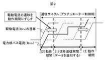
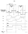
- FIG. 2 is a diagram illustrating the control operation of the operation timing control circuit 3212.
- the operation timing control circuit 3212 communicates the transition timing of the drive current Idrv (the transition timing of the drive current Idrv to the drive circuit 322 rising from off (Low) to on (High) or falling from on to off).
- (2) Transition operation period (shown in the figure) in which the transition timing is provided before and after the signal transmission period. During the operation period).
- the power line bus current Ibus does not change in driving current because no transition occurs in the driving current within the (1) signal transmission period of the communication cycle.
- the rising timing of the drive current Idrv is shown to be shifted forward in time.
- the drive current Idrv is controlled to be shifted relative to the signal transmission period.
- the current for controlling the actuator 33 average current of the drive current Idrv
- the frequency at which the drive current Idrv changes and the communication frequency are generally 3 to 4 orders of magnitude different, so the variation is negligible.
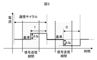
- FIG. 3 is a current waveform diagram showing the operation of the current modulation circuit 311.
- the modulation by the current modulation circuit 311 changes the current transition direction with respect to a predetermined reference current according to the sign of the transmission data.
- the current modulation circuit 311 has a transmission current waveform corresponding to a predetermined reference current when the sign of the data DSA from the actuator control circuit 321 via the communication control circuit 313 is “1” within the signal transmission period.
- the transmission current waveform When the positive transition (+ ⁇ Ip) occurs and the sign of the data DSA is “0”, the transmission current waveform generates a transmission current waveform in which a negative transition ( ⁇ Ip) occurs with respect to a predetermined reference current, This transmission current waveform is superimposed on the power line bus current Ibus.
- the current detection circuit 221 detects the current Ibus of the power line bus 4 and is similar to the waveform of the power line bus current (current waveform transitioning to the positive side or the negative side with respect to a predetermined reference current) Convert to a simple voltage waveform. Therefore, the output waveform of the current detection circuit 221 is also a voltage waveform like the current waveform shown in FIG.
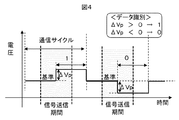
- FIG. 4 is a diagram showing an identification method for identifying the code from the output waveform of the current detection circuit 221 by the reception identification circuit 222.
- the reception identification circuit 222 In the case of “1” and transition to the negative side with respect to a predetermined reference voltage ( ⁇ Vp ⁇ 0), “0” and the sign of the received data Dir are identified.
- the signal transmission period can be said to be a signal reception period, but the terms are used here in a unified manner.
- communication using the power line can be realized in a situation where power supply from the DC power supply to the power line is continued. Specifically, by changing the transition timing of the drive current Idrv of the actuator 33 to the operation period provided in the communication cycle, it is possible to prevent current fluctuation due to drive control of the actuator 33 during the signal transmission period. As a result, current communication in the power line communication device by the actuator 3 having the communication function and the control station communication block 2 does not cause a communication error by exchanging data within the communication period.
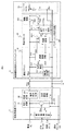
- FIG. 5 is a configuration example of an electronic control device provided with the power line communication device of the present embodiment. However, illustration of the ECU 1 and the power source 5 is omitted.
- the present embodiment is an electronic control device in which a solenoid coil is applied to the actuator 33 of the first embodiment.
- the drive circuit 322 has two switches SW1 and SW2. These two switches operate complementarily by the operation timing signal OPdrv from the operation timing control circuit 3212. When the switch SW1 is on, the switch SW2 is turned off, and when the switch SW1 is off, the switch SW2 is turned on.
- the average current of the drive current Idrv flowing through the solenoid coil 33 is controlled by the time width when the switch SW1 is turned on with respect to the ON / OFF cycle of the switch SW1, that is, the pulse width of the operation timing signal OPdrv that turns on the switch SW1. That is, the drive current Idrv is PWM (pulse width modulation) controlled by the operation timing signal OPdrv.
- the operation timing signal OPdrv for turning on the switch SW1 is such that the transition timing of the control pulse (OP) generated by the control circuit 3211 of the actuator control circuit 321 is controlled during the operation period in the communication cycle.
- the frequency of the control pulse (OP) is several hundreds Hz (switch SW1 on / off switching frequency). Therefore, the drive current Idrv of the solenoid coil 33 varies at several hundred Hz.
- communication frequencies communication clocks CK and CKA
- the frequency of the control pulse (OP) differs from the communication frequency by 3 to 4 digits. Therefore, the fluctuation of the average current of the drive current Idrv accompanying the control to the operation period in the communication cycle of the transition timing of the control pulse (OP) can be ignored.
- FIG. 6 is a configuration example of the actuator control circuit 321 focusing on the output of the control pulse OP.
- the actuator control circuit 321 includes a control circuit 3211 and an operation timing control circuit 3212.
- the control circuit 3211 includes a current setting circuit 32111 that stores a set current value corresponding to a command value (control command) from the ECU 1, a current monitor circuit 32115 that monitors a current value flowing through the solenoid coil 33, a set current value and a current monitor circuit It has a difference circuit 32112 that outputs a difference from a current value (current monitor result) flowing through the solenoid coil 33 monitored by 32115, a triangular wave generation circuit 32114 that generates a PWM control pulse, and a difference circuit 32113.
- the control circuit 3211 outputs a control pulse OP having a pulse width corresponding to the difference output of the difference circuit 32112, and performs control so that the set current value matches the current monitor result. That is, when the set current value matches the current value of the solenoid coil 33, the control circuit 3211 outputs a control pulse OP having a predetermined pulse width, and when the set current value is larger, the control circuit 3211 A control pulse OP having a larger pulse width is output.
- control circuit 3211 transmits the transmission data to the control station communication block 2.
- the transmission data is control state data of the actuator 33, for example, a current monitor result.
- the transmission data is output from the control circuit 3211 to the communication control circuit 313 in synchronization with the communication clock CKA.
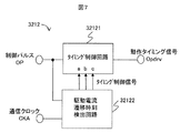
- FIG. 7 shows a configuration example of the operation timing control circuit 3212.
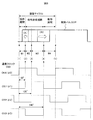
- FIG. 8 is a timing chart showing the operation of the operation timing control circuit 3212.
- the operation timing control circuit 3212 includes a timing control circuit 32121 and a drive current transition time detection circuit 32122.
- the timing control circuit 32121 receives the control pulse OP from the control circuit 3211 and the timing control signals a, b, and c from the drive current transition time detection circuit 32122, and outputs the operation timing signal Opdrv.
- the drive current transition time detection circuit 32122 receives the control pulse OP and the communication clock CKA, and outputs timing control signals a, b, and c to the timing control circuit 32121.
- FIG. 8 is a timing chart showing the operation of the operation timing control circuit 3212.
- the drive current transition time detection circuit 32122 uses the communication clock CKA as the basic clock CKA ( ⁇ 0), the clock CK1 delayed by ⁇ 1 (for example, 60 °) from CKA, the clock CK2 delayed by ⁇ 2 (for example, 120 °) by CKA, and A clock CK3 delayed by ⁇ 3 (for example, 240 °) from CKA is used.
- the clocks CK1 to CK3 are generated from the communication clock CKA by the drive current transition time detection circuit 32122, as will be described later.
- One cycle of the communication clock CKA is called a communication cycle as described above.
- the communication cycle is divided into four windows W1 to W4.
- the window W1 is between (1) the rising time of CKA and (2) the rising time of CK1.
- the window W2 is between (2) the rising time of CK1 and (3) the rising time of CK2.
- the window W3 is between (3) the rising time of CK2 and (4) the rising time of CK3.
- the window W4 is from (4) the rising time of CK3 to (5) the rising time of the next cycle of CKA (communication cycle end time).
- the drive current transition time detection circuit 32122 detects the level (High or Low) of the control pulse OP (input from the difference circuit 32113) at the start and end times (1) to (5) of each window.
- the difference exceeds a predetermined threshold value
- the drive current transition time detection circuit 32122 outputs a high level “1” to the timing control signal a if the edge is switched to the window W2 and is high to the timing control signal c if the edge is switched to the window W3. If level “1” is output and there is no switching edge in windows W2 and W3, high level “1” is output to timing control signal b.
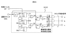
- FIG. 9A is a specific example of the drive current transition time detection circuit 32122.
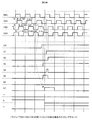
- FIG. 9B is a timing chart of the case where there is a switching edge of the control pulse OP in the window W3 of the drive current transition time detection circuit 32122 as an example.
- D1, D2, and D3 are delay circuits for generating clocks CK1 to CK3 having delay times from the communication clock CKA.
- the delay circuit D1 has a delay time D1 corresponding to the aforementioned phase ⁇ 1.
- the delay circuit D2 has a delay time D2 corresponding to the aforementioned phase ( ⁇ 2 ⁇ 1).
- the delay circuit D3 has a delay time D3 corresponding to the aforementioned phase ( ⁇ 3- ⁇ 2- ⁇ 1).
- the delay time D1 is the delay time of CK1 with respect to CKA
- the delay time D2 is the delay time of CK2 with respect to CK1
- the delay time D3 is the delay time of CK3 with respect to CK2. is there.
- the latch circuit (not shown in the figure) outputs signals S1, S2, and S3 obtained by latching the control pulse OP at the rising edges of CK1, CK2, and CK3, respectively.
- the sample hold circuit SH holds the output S4 of the exclusive OR circuit for the signals S1 and S2 and the output S5 of the exclusive OR circuit for the signals S2 and S3, respectively, and outputs them as S6 and S7.
- the output S4 of the exclusive OR circuit represents the presence of the switching edge of the control pulse OP in the window W2, and the output S5 of the exclusive OR circuit represents the presence of the switching edge of the control pulse OP in the window W3.
- the output S5 of the exclusive OR circuit is held by the sample hold circuit SH and outputs “1” (High) to the timing control signal c as exemplified in FIG. 9B.
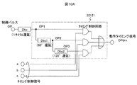
- FIG. 10A is a specific example of the timing control circuit 32121.
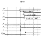
- FIG. 10B is a timing chart illustrating an example in which the timing edge of the control pulse OP is present in the window W3 of the timing control circuit 32121.
- the timing control signal a of the drive current transition time detection circuit 32122 is “1”
- the timing control circuit 32121 advances the phase of the control pulse OP compared to when the timing control signal b is “1”.
- the signal c is “1”
- the phase of the control pulse OP is delayed compared to when the timing control signal b is “1” and is output as the operation timing signal OPdrv.
- the delay time tc of the delay circuit Dtc is set to the time of one cycle (communication cycle) of the communication clock CKA.
- the delay time ts1 of the delay circuit Dts1 is set to the window width of the window W2.
- the delay time ts2 of the delay circuit Dts2 is set to the window width of the window W3.
- the control pulse OP obtains OP1 delayed by the delay time tc, OP2 delayed by the delay time tc + ts1, and OP3 delayed by the delay time tc + ts1 + ts2.
- the operation timing signal OPdrv is earlier by the delay time ts1 when the timing control signal a is “1” than when the timing control signal b is “1”.
- the operation timing signal OPdrv is delayed by a delay time ts2 when the timing control signal c is “1” compared to when the timing control signal b is “1”. Therefore, the switching edge of the control pulse OP moves to the operation period described above and does not exist in the signal transmission period.
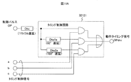
- FIG. 11A shows another specific example of the timing control circuit 32121.
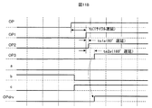
- FIG. 11B is a timing chart of another timing control circuit 32121 as an example in which there is a switching edge of the control pulse OP in the window W3.
- the operation timing signal OPdrv is advanced by the delay time ts1a when the timing control signal b is “1”, when the a is “1”, and the delay time ts2a ⁇ when the c is “1”.
- a signal delayed by ts1a is output.
- the delay time ts1a is set to the window width of the window W2, and the difference between the delay time Ts1a and the delay time Ts2a is set to the window width of the window W3, thereby operating similarly to the timing control circuit 32121 of FIG. 11A. Since FIG. 11A and FIG. 11B can be understood in combination with the description of FIG. 10A and FIG. 10B, detailed description thereof will be omitted.
- FIG. 12 is a specific example of the current demodulating circuit 22.
- the current demodulation circuit 22 includes the current detection circuit 221 and the reception identification circuit 222 as described above.
- the current detection circuit 221 includes a resistor 2212 and a differential amplifier circuit 2211.
- the differential amplifier circuit 2211 amplifies the voltage drop of the power line bus current Ibus due to the resistor 2212, that is, the voltage difference (V2 ⁇ V1) across the resistor 2212, and outputs a voltage signal n1.
- the reception identification circuit 222 includes three sample and hold circuits (SH) 2221, 2222, and 2224, a difference circuit 2223, and a clock generation circuit 2225.
- the reception identification circuit 222 identifies the output voltage signal n1 of the current detection circuit 221 and converts it into reception data.
- FIG. 13 is a timing chart showing the operation of the reception identification circuit 222.
- the output voltage signal n1 of the current detection circuit 221 is held by the sample and hold circuits 2221 and 2222 as voltage signals n2 and n3, respectively, with two phases ⁇ 5 and ⁇ 6 within the signal transmission period.
- the reception identification circuit 222 obtains the difference n4 between the voltage signals of the sample and hold circuits 2221 and 2222 by the difference circuit 2223, synchronizes the difference voltage signal n4 with the clock of the phase ⁇ 4, and outputs the reception data n5 (Dir). Therefore, the reception identifying circuit 222 identifies the received data in synchronization with the communication clock (phase ⁇ 4) with the data in the signal transmission period.
- the communication clock CKA of the clock generation circuit 2225 of the reception identification circuit 222 is generated by receiving data n5 via a PLL (Phase Locked Loop) circuit and phase adjustment (delay), although not shown.
- PLL Phase Locked Loop
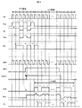
- FIG. 14 is a timing chart outlining communication between the control station communication block 2 and the actuator 3 having a communication function.
- the transmission data Dos is voltage-modulated in the voltage modulation circuit 21 in synchronization with the communication clock CK from the ECU 1, superimposed on the power supply voltage Vb, and input to the communication block 31 as Vbus.
- the voltage demodulation circuit 312 demodulates the voltage of Vbus and converts it into data Rd.
- the data Rd is output to the drive block 32 via the communication control circuit 313.
- the uplink communication is current communication synchronized with the communication clock CKA generated by the communication control circuit 313.
- the communication control circuit 313 outputs the data from the actuator control circuit 321 to the current modulation circuit 311 as transmission data DSA.
- the current modulation circuit 311 generates a transmission current waveform corresponding to the transmission data DSA, and superimposes this transmission current waveform on the power line bus current Ibus.
- the transmission current waveform superimposed on the power line bus current Ibus is identified by the current detection circuit 221 and the reception identification circuit 222 and output to the communication logic circuit 23 as reception data Dir.
- the transition timing of the drive current Idrv according to the control pulse OP that is the output of the control circuit is the operation timing signal of the operation timing control circuit 3212 during the operation period (see FIG. 2) in the communication cycle determined by the communication clock CKA. Since it is shifted by OPdrv, as shown in the figure, the transmission current waveform corresponding to the transmission data DSA is synchronized with the communication clock CKA and does not cause an error.
- communication using the power line can be realized in a situation where power supply from the DC power supply to the power line is continued.
- the control circuit 3211 controls the PWM control pulse width, and is controlled by the operation timing control circuit 3212 so that the transition of the PWM control pulse does not occur in the signal transmission period. Therefore, current communication between the actuator 3 and the control station communication block 2 does not cause a communication error by exchanging data within the communication period.
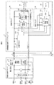
- FIG. 15 is a configuration example of an electronic control device including the power line communication device of the present embodiment, and is an example in which the communication block 31 of the actuator 3 having the communication function of the first embodiment is replaced with another configuration.
- a series circuit (ringing prevention series circuit) 314 of a capacitor 3141 and a resistor 3142 is connected between two power lines.
- Series circuit 314 suppresses the ringing phenomenon of power line bus current Ibus generated by the inductance component of the power line. By suppressing the ringing phenomenon of the power line bus current Ibus by the series circuit 314, it is possible to suppress a malfunction of detection of the transition time of the drive current Idrv by the drive current transition time detection circuit 32122.
- FIG. 16 is a configuration example of an electronic control device including the power line communication device of the present embodiment, in the actuator 3 having the communication function of the first embodiment, the detection block 34 having the drive block 32 and the power source Vb in common.
- the actuator 3 having a communication function includes a communication block 31, a drive block 32, an actuator 33, a detection block 34, and a sensor 35.
- the communication block 31 communicates with the control station communication block 2 and exchanges transmission / reception data between the drive block 32 of the actuator 33 and the detection block 34 of the sensor 34.
- the detection block 34 has a sensor control circuit 341 and an ADC (analog / digital conversion circuit) 342.
- the sensor control circuit 341 outputs the sensor control data to the ADC 342 based on the control data of the sensor 35 via the communication block 31, and the sensor data from the sensor 35 converted into digital data by the ADC 342 to the communication block 31. Output.
- the ADC 342 converts the sensor control data from the sensor control circuit 341 into an analog signal and outputs it to the sensor 35, and converts the analog sensor data from the sensor 35 into digital data and outputs it to the sensor control circuit 341.
- the sensor 35 may incorporate an ADC 342.
- Sensor data is transmitted by the communication block 31 at the same timing (signal transmission period) as the transmission data from the actuator control circuit 321.
- communication using the power line can be realized in a situation where power supply from the DC power supply to the power line is continued.
- the detection block 34 and the sensor 35 generally do not have a factor that causes the power supply Vb to fluctuate like the PWM control of the drive block 32 and the actuator 33. Therefore, the current communication timing by the communication block 31 may be controlled as described in the first embodiment. Therefore, also in this embodiment, the current communication between the actuator 3 and the control station communication block 2 does not cause a communication error by exchanging data within the communication period.
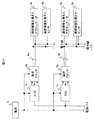
- FIG. 17 is a configuration example in which the first embodiment is applied as an electronic control device in which a plurality of ECUs 1a and 1b are connected to a power source 5 by a bus.
- Each ECU 1a, 1b is connected to a power line communication device.
- the power line communication device connected to the ECU 1a includes an actuator 3a having a communication function and a sensor 3b having a communication function on the power line 4a connected to the communication block 2a.
- the power line communication device connected to the ECU 1b has the same configuration.
- the sensor 3b having a communication function is, for example, the actuator 3 having a communication function excluding the drive block 32 and the actuator 33 in FIG.
- communication using the power line can be realized in a situation where power supply from the DC power supply to the power line is continued.
- the actuators 3a and 3c are controlled in the same manner as in the first embodiment. Therefore, the actuator having the communication function and the sensors 3a to 3d having the communication function and the control station communication block 2a The current communication with 2b does not cause a communication error by exchanging data within the communication period.
- communication using a power line can be realized in a situation where power supply from the DC power supply to the power line is continued.
Landscapes
- Engineering & Computer Science (AREA)
- Computer Networks & Wireless Communication (AREA)
- Signal Processing (AREA)
- Power Engineering (AREA)
- Physics & Mathematics (AREA)
- Spectroscopy & Molecular Physics (AREA)
- Dc Digital Transmission (AREA)
- Cable Transmission Systems, Equalization Of Radio And Reduction Of Echo (AREA)
Abstract
Description
Claims (15)
- アクチュエータを制御する制御パルスを生成し、通信クロックによる通信サイクル内に設定した動作期間に、前記制御パルスの遷移タイミングを制御するアクチュエータ制御回路、および、前記遷移タイミングを制御された前記制御パルスに基づいて、直流電源から電力線を通して供給される前記アクチュエータの駆動電流を制御する駆動回路を含む駆動ブロック、並びに、
前記通信クロックを生成し、前記通信サイクル内に設定した、前記動作期間とは異なる信号送信期間に、送信するデータに応じて、前記電力線に流れる電流を変調する通信ブロックを有することを特徴とする電力線通信装置。 - 前記アクチュエータ制御回路は、前記制御パルスの前記遷移タイミングを制御する動作タイミング制御回路を含むことを特徴とする請求項1記載の電力線通信装置。
- 前記通信ブロックによる前記電力線に流れる電流の変調は、所定の基準電流に対して前記電流を遷移させることを特徴とする請求項2記載の電力線通信装置。
- 前記所定の基準電流に対する前記電流の遷移は、前記データが1のとき立ち上り遷移であり、前記データが0のとき立ち下り遷移であることを特徴とする請求項3記載の電力線通信装置。
- 前記通信ブロックに前記電力線を介して接続し、前記電力線に流れる、前記所定の基準電流に対する前記電流の遷移を検出し、検出した前記遷移の方向に基づいて前記データの符号を識別する電流復調回路を有することを特徴とする請求項4記載の電力線通信装置。
- 前記通信ブロックは、前記電力線にリンギング防止用直列回路を接続することを特徴とする請求項1記載の電力線通信装置。
- ECU(Electronic Control Unit)からアクチュエータを制御するための制御指令を送信し、前記アクチュエータの制御状態情報のデータを受信する第1の通信ブロック、
前記制御指令に対応した、前記アクチュエータを制御する制御パルスを生成し、通信クロックによる通信サイクル内に設定した動作期間に、前記制御パルスの遷移タイミングを制御するアクチュエータ制御回路、および、前記遷移タイミングを制御された前記制御パルスに基づいて、直流電源から電力線を通して供給される前記アクチュエータの駆動電流を制御する駆動回路を含む駆動ブロック、並びに、
前記第1の通信ブロックと前記電力線を介して接続し、前記通信クロックを生成し、前記通信サイクル内に設定した、前記動作期間とは異なる信号送信期間に、前記第1の通信ブロックへ送信する前記データに応じて、前記電力線に流れる電流を変調する第2の通信ブロックを有することを特徴とする電子制御装置。 - 前記アクチュエータ制御回路は、前記制御パルスの前記遷移タイミングを制御する動作タイミング制御回路を含むことを特徴とする請求項7記載の電子制御装置。
- 前記第2の通信ブロックによる前記電力線に流れる電流の変調は、所定の基準電流に対して前記電流を遷移させることを特徴とする請求項8記載の電子制御装置。
- 前記所定の基準電流に対する前記電流の遷移は、前記データの符号が1のとき立ち上り遷移であり、前記データの符号が0のとき立ち下り遷移であることを特徴とする請求項9記載の電子制御装置。
- 前記第1の通信ブロックは、前記電力線に流れる、前記所定の基準電流に対する前記電流の遷移を検出し、検出した前記遷移の方向に基づいて前記データの符号を識別する電流復調回路を有することを特徴とする請求項10記載の電子制御装置。
- 前記第1の通信ブロックは、前記制御指令を電圧変調し、前記電力線を介して送信することを特徴とする請求項7記載の電子制御装置。
- 前記第2の通信ブロックは、前記電力線にリンギング防止用直列回路を接続することを特徴とする請求項7記載の電子制御装置。
- センサからのセンサデータを前記第2の通信ブロックへ出力する検出ブロックを有し、
前記第2の通信ブロックは、前記信号送信期間に、前記第1の通信ブロックへ送信する前記センサデータに応じて、前記電力線に流れる電流を変調することを特徴とする請求項7記載の電子制御装置。 - 前記ECU、前記第1の通信ブロック及び前記第2の通信ブロックを有する複数の構成を、前記電力線を介して前記直流電源に接続することを特徴とする請求項7記載の電子制御装置。
Priority Applications (5)
| Application Number | Priority Date | Filing Date | Title |
|---|---|---|---|
| DE112016005568.4T DE112016005568B4 (de) | 2016-01-04 | 2016-01-04 | Leistungsleitungs-kommunikationsvorrichtung und elektronische steuervorrichtung, die eine leistungsleitungs-kommunikationsvorrichtung enthält |
| CN201680073193.0A CN108370260B (zh) | 2016-01-04 | 2016-01-04 | 电力线通信装置以及具备电力线通信装置的电子控制装置 |
| JP2017559953A JP6518793B2 (ja) | 2016-01-04 | 2016-01-04 | 電力線通信装置、および電力線通信装置を備えた電子制御装置 |
| PCT/JP2016/050032 WO2017119054A1 (ja) | 2016-01-04 | 2016-01-04 | 電力線通信装置、および電力線通信装置を備えた電子制御装置 |
| US16/067,663 US10498395B2 (en) | 2016-01-04 | 2016-01-04 | Power line communication apparatus and electronic control apparatus including power line communication apparatus |
Applications Claiming Priority (1)
| Application Number | Priority Date | Filing Date | Title |
|---|---|---|---|
| PCT/JP2016/050032 WO2017119054A1 (ja) | 2016-01-04 | 2016-01-04 | 電力線通信装置、および電力線通信装置を備えた電子制御装置 |
Publications (1)
| Publication Number | Publication Date |
|---|---|
| WO2017119054A1 true WO2017119054A1 (ja) | 2017-07-13 |
Family
ID=59273433
Family Applications (1)
| Application Number | Title | Priority Date | Filing Date |
|---|---|---|---|
| PCT/JP2016/050032 Ceased WO2017119054A1 (ja) | 2016-01-04 | 2016-01-04 | 電力線通信装置、および電力線通信装置を備えた電子制御装置 |
Country Status (5)
| Country | Link |
|---|---|
| US (1) | US10498395B2 (ja) |
| JP (1) | JP6518793B2 (ja) |
| CN (1) | CN108370260B (ja) |
| DE (1) | DE112016005568B4 (ja) |
| WO (1) | WO2017119054A1 (ja) |
Cited By (1)
| Publication number | Priority date | Publication date | Assignee | Title |
|---|---|---|---|---|
| WO2018179483A1 (ja) * | 2017-03-27 | 2018-10-04 | 日立オートモティブシステムズ株式会社 | 負荷駆動システムおよび負荷駆動方法 |
Families Citing this family (7)
| Publication number | Priority date | Publication date | Assignee | Title |
|---|---|---|---|---|
| DE102016119548A1 (de) * | 2016-10-13 | 2018-04-19 | Endress+Hauser SE+Co. KG | Verfahren zur Datenübertragung zwischen einem Feldgerät der Automatisierungstechnik und einer Kommunikationsbox |
| CN109923790B (zh) * | 2016-11-10 | 2021-10-08 | 株式会社自动网络技术研究所 | 车载通信系统 |
| US10847979B2 (en) * | 2018-12-14 | 2020-11-24 | Zhuhai Jieli Technology Co., Ltd | Charging and communication system |
| CN109672477B (zh) * | 2019-01-29 | 2023-08-29 | 四川天源宏创科技有限公司 | 一种基于脉冲密度调制的声阵列供电与命令下行复用系统及其控制方法 |
| KR102767187B1 (ko) * | 2019-12-26 | 2025-02-13 | 삼성전자주식회사 | 모바일 장치 및 상기 모바일 장치의 동작 방법 |
| US11552676B2 (en) | 2020-02-11 | 2023-01-10 | Samsung Electronics Co., Ltd. | Mobile device for performing power line communication and operating method thereof |
| FR3114680B1 (fr) * | 2020-09-30 | 2023-01-20 | Schneider Electric Ind Sas | Dispositif de communication pour un appareil de commutation électrique |
Citations (3)
| Publication number | Priority date | Publication date | Assignee | Title |
|---|---|---|---|---|
| JP2007306209A (ja) * | 2006-05-10 | 2007-11-22 | Denso Corp | 通信装置 |
| JP2010081340A (ja) * | 2008-09-26 | 2010-04-08 | Denso Corp | 差動通信装置 |
| WO2012056927A1 (ja) * | 2010-10-27 | 2012-05-03 | 株式会社オートネットワーク技術研究所 | 電力線通信システム |
Family Cites Families (31)
| Publication number | Priority date | Publication date | Assignee | Title |
|---|---|---|---|---|
| US5691898A (en) * | 1995-09-27 | 1997-11-25 | Immersion Human Interface Corp. | Safe and low cost computer peripherals with force feedback for consumer applications |
| JP3262046B2 (ja) * | 1997-09-17 | 2002-03-04 | トヨタ自動車株式会社 | ギヤ機構における歯打ち音の低減方法、動力出力装置およびこの動力出力装置を搭載したハイブリッド車輌 |
| US6498698B1 (en) * | 1999-06-29 | 2002-12-24 | Western Digital Technologies, Inc. | Servowriter employing method of unlatching actuator arm using VCM voltage limiting circuit to limit actuator arm velocity |
| DE10248456A1 (de) * | 2001-10-19 | 2003-06-18 | Denso Corp | Fahrzeugkommunikationssystem |
| JP3994956B2 (ja) * | 2002-12-18 | 2007-10-24 | ソニー株式会社 | ロボット装置、並びに負荷吸収装置及び負荷吸収方法 |
| US6989645B2 (en) * | 2002-12-18 | 2006-01-24 | Sony Corporation | Robot apparatus, and load absorbing apparatus and method |
| JP4263023B2 (ja) * | 2003-06-02 | 2009-05-13 | パナソニック株式会社 | 2線式データ通信方法、システム、コントロール装置およびデータ記憶装置 |
| US7652390B2 (en) * | 2004-12-28 | 2010-01-26 | Calix Networks, Inc. | Network interface device communication via power line |
| US7889476B2 (en) * | 2006-09-22 | 2011-02-15 | Siemens Industry, Inc. | Electronics for multipole remote operated relay |
| US8248762B2 (en) * | 2006-09-22 | 2012-08-21 | Siemens Industry, Inc. | Reliable asynchronous serial protocol between remote operated devices and input/output controller |
| JP2008259361A (ja) * | 2007-04-06 | 2008-10-23 | Mitsuba Corp | 電動車両用駆動装置 |
| JP4600453B2 (ja) * | 2007-09-26 | 2010-12-15 | セイコーエプソン株式会社 | 送電制御装置、送電装置、受電装置、無接点電力伝送システム、電子機器、2次コイル位置検出方法および1次コイルの位置決め方法 |
| JP5046345B2 (ja) * | 2008-05-29 | 2012-10-10 | 株式会社オートネットワーク技術研究所 | 通信装置、及び通信システム |
| DE102009041481A1 (de) | 2008-09-16 | 2010-04-29 | Denso Corporation, Kariya-City | Elektronische Vorrichtung |
| JP5515032B2 (ja) * | 2009-06-24 | 2014-06-11 | 国立大学法人京都大学 | 雑音検出方法、雑音検出装置、シミュレーション方法、シミュレーション装置、及び通信システム |
| US8659183B2 (en) * | 2009-07-17 | 2014-02-25 | Rain Bird Corporation | Variable initialization time in the charging of energy reserves in an irrigation control system |
| CN102076077B (zh) * | 2009-11-24 | 2015-01-28 | 中兴通讯股份有限公司 | 一种上行同步控制方法、系统和基站 |
| EP2485406B1 (en) * | 2011-02-07 | 2017-03-15 | Sony Corporation | Power line communication apparatus including ac power socket |
| EP2672632A4 (en) * | 2011-03-10 | 2014-07-23 | Panasonic Corp | Power line communication device, power line communication system, power line communication method, and power line communication program |
| US8816830B2 (en) * | 2011-08-19 | 2014-08-26 | Legendaire Technology Co., Ltd. | Motor control system and the method of controlling motor |
| US11199824B2 (en) * | 2012-01-17 | 2021-12-14 | Fisher-Rosemount Systems, Inc. | Reducing controller updates in a control loop |
| US9641122B2 (en) * | 2012-06-26 | 2017-05-02 | Johnson Controls Technology Company | HVAC actuator with automatic end stop recalibration |
| AT513542B1 (de) * | 2012-11-15 | 2014-07-15 | Fronius Int Gmbh | Verfahren und Anordnung zur Datenkommunikation zwischen einem Wechselrichter und einer Netzüberwachungseinheit |
| TWI504182B (zh) * | 2013-04-19 | 2015-10-11 | 東林科技股份有限公司 | A method of transmitting a signal using a power waveform |
| US9374855B2 (en) * | 2013-10-24 | 2016-06-21 | Osram Sylvania Inc. | Power line communication for lighting systems |
| JP6060878B2 (ja) * | 2013-11-20 | 2017-01-18 | トヨタ自動車株式会社 | 送受電部を備えた車両 |
| US9191038B2 (en) * | 2013-12-24 | 2015-11-17 | Shimano Inc. | Wireless bicycle communication apparatus and wireless bicycle communication system |
| CN103840485B (zh) * | 2014-02-28 | 2015-02-25 | 山东大学 | 分布式并网逆变系统全局同步脉宽调制系统及方法 |
| US10009100B2 (en) * | 2014-06-18 | 2018-06-26 | Qualcomm Incorporated | Transmission of identifiers using visible light communication |
| US9739840B2 (en) * | 2015-02-12 | 2017-08-22 | Tri-Tec Manufacturing, LLC | Power detection system for valve actuators |
| US10727782B2 (en) * | 2015-05-12 | 2020-07-28 | Dennis Peet | Schedule-based sun tracker for increasing directness of sun exposure upon a solar panel to improve energy production |
-
2016
- 2016-01-04 WO PCT/JP2016/050032 patent/WO2017119054A1/ja not_active Ceased
- 2016-01-04 CN CN201680073193.0A patent/CN108370260B/zh active Active
- 2016-01-04 US US16/067,663 patent/US10498395B2/en active Active
- 2016-01-04 DE DE112016005568.4T patent/DE112016005568B4/de active Active
- 2016-01-04 JP JP2017559953A patent/JP6518793B2/ja active Active
Patent Citations (3)
| Publication number | Priority date | Publication date | Assignee | Title |
|---|---|---|---|---|
| JP2007306209A (ja) * | 2006-05-10 | 2007-11-22 | Denso Corp | 通信装置 |
| JP2010081340A (ja) * | 2008-09-26 | 2010-04-08 | Denso Corp | 差動通信装置 |
| WO2012056927A1 (ja) * | 2010-10-27 | 2012-05-03 | 株式会社オートネットワーク技術研究所 | 電力線通信システム |
Non-Patent Citations (1)
| Title |
|---|
| ARABIA, E. ET AL.: "Electromechanical actuators for automotive applications exploiting power line communication, International Symposium on Power Electronics, Electrical Drives", POWER ELECTRONICS, ELECTRICAL DRIVES, AUTOMATION AND MOTION, 2006. SPE EDAM 2006. INTERNATIONAL SYMPOSIUM ON TAORMINA, ITALY MAY, 23RD - 26TH, 2006, 23 May 2006 (2006-05-23), pages 909 - 914, XP010924617, DOI: 10.1109/SPEEDAM.2006.1649897 * |
Cited By (1)
| Publication number | Priority date | Publication date | Assignee | Title |
|---|---|---|---|---|
| WO2018179483A1 (ja) * | 2017-03-27 | 2018-10-04 | 日立オートモティブシステムズ株式会社 | 負荷駆動システムおよび負荷駆動方法 |
Also Published As
| Publication number | Publication date |
|---|---|
| JP6518793B2 (ja) | 2019-05-22 |
| JPWO2017119054A1 (ja) | 2018-08-02 |
| US10498395B2 (en) | 2019-12-03 |
| DE112016005568B4 (de) | 2021-10-21 |
| DE112016005568T5 (de) | 2018-09-06 |
| CN108370260B (zh) | 2021-04-30 |
| US20190007100A1 (en) | 2019-01-03 |
| CN108370260A (zh) | 2018-08-03 |
Similar Documents
| Publication | Publication Date | Title |
|---|---|---|
| JP6518793B2 (ja) | 電力線通信装置、および電力線通信装置を備えた電子制御装置 | |
| US7656687B2 (en) | Modulated transformer-coupled gate control signaling method and apparatus | |
| US10067895B2 (en) | Systems and methods for asynchronous toggling of I2C data line | |
| US10700741B2 (en) | Electronic control apparatus provided with power line communication function, actuator, electronic control system, and automobile using same | |
| US9252655B2 (en) | Phase shift circuit and power factor correction circuit including the same | |
| JP2005080256A (ja) | 制御・監視信号伝送システム | |
| JP4760955B2 (ja) | 負荷駆動装置及び負荷駆動装置の制御システム | |
| US10063050B2 (en) | Power supply system and power supply apparatus | |
| CA2766342A1 (en) | Method and device for programming a microcontroller | |
| US7079589B1 (en) | Serial digital communication superimposed on a digital signal over a single wire | |
| JP4250634B2 (ja) | データ通信装置、データ通信システム及びデータ通信方法 | |
| JP4089445B2 (ja) | 半導体集積回路装置 | |
| CN202276287U (zh) | 在脉宽调制控制中补偿死区时间的控制系统 | |
| TW200644553A (en) | Synchronization circuits and methods | |
| US9239027B2 (en) | Motor control device | |
| JP6191698B2 (ja) | 電源システム | |
| JP5388953B2 (ja) | 制御・監視信号リモート伝送システム | |
| JP5072813B2 (ja) | 出力ターミナル及び制御・監視信号伝送システム | |
| JP3654103B2 (ja) | スイッチ制御回路 | |
| US20150042637A1 (en) | Source driver and operation method thereof | |
| KR102087771B1 (ko) | 무선으로 전송된 입력전력의 주파수 변화에 적응하는 동기식 정류장치 | |
| CN116470888A (zh) | Dtof驱动电路的延迟时间控制电路 | |
| JP2004280617A (ja) | 電源回路及び電源供給制御装置 | |
| JP2008072637A (ja) | 位相比較信号処理回路 | |
| JP2009153284A (ja) | ステッピングモータ制御装置 |
Legal Events
| Date | Code | Title | Description |
|---|---|---|---|
| 121 | Ep: the epo has been informed by wipo that ep was designated in this application |
Ref document number: 16883559 Country of ref document: EP Kind code of ref document: A1 |
|
| ENP | Entry into the national phase |
Ref document number: 2017559953 Country of ref document: JP Kind code of ref document: A |
|
| WWE | Wipo information: entry into national phase |
Ref document number: 112016005568 Country of ref document: DE |
|
| 122 | Ep: pct application non-entry in european phase |
Ref document number: 16883559 Country of ref document: EP Kind code of ref document: A1 |