WO2017117847A1 - 多路复用型显示驱动电路 - Google Patents
多路复用型显示驱动电路 Download PDFInfo
- Publication number
- WO2017117847A1 WO2017117847A1 PCT/CN2016/074466 CN2016074466W WO2017117847A1 WO 2017117847 A1 WO2017117847 A1 WO 2017117847A1 CN 2016074466 W CN2016074466 W CN 2016074466W WO 2017117847 A1 WO2017117847 A1 WO 2017117847A1
- Authority
- WO
- WIPO (PCT)
- Prior art keywords
- electrically connected
- thin film
- film transistor
- sub
- pixel
- Prior art date
- Legal status (The legal status is an assumption and is not a legal conclusion. Google has not performed a legal analysis and makes no representation as to the accuracy of the status listed.)
- Ceased
Links
Images
Classifications
-
- G—PHYSICS
- G09—EDUCATION; CRYPTOGRAPHY; DISPLAY; ADVERTISING; SEALS
- G09G—ARRANGEMENTS OR CIRCUITS FOR CONTROL OF INDICATING DEVICES USING STATIC MEANS TO PRESENT VARIABLE INFORMATION
- G09G3/00—Control arrangements or circuits, of interest only in connection with visual indicators other than cathode-ray tubes
- G09G3/20—Control arrangements or circuits, of interest only in connection with visual indicators other than cathode-ray tubes for presentation of an assembly of a number of characters, e.g. a page, by composing the assembly by combination of individual elements arranged in a matrix no fixed position being assigned to or needed to be assigned to the individual characters or partial characters
- G09G3/34—Control arrangements or circuits, of interest only in connection with visual indicators other than cathode-ray tubes for presentation of an assembly of a number of characters, e.g. a page, by composing the assembly by combination of individual elements arranged in a matrix no fixed position being assigned to or needed to be assigned to the individual characters or partial characters by control of light from an independent source
- G09G3/36—Control arrangements or circuits, of interest only in connection with visual indicators other than cathode-ray tubes for presentation of an assembly of a number of characters, e.g. a page, by composing the assembly by combination of individual elements arranged in a matrix no fixed position being assigned to or needed to be assigned to the individual characters or partial characters by control of light from an independent source using liquid crystals
- G09G3/3611—Control of matrices with row and column drivers
- G09G3/3674—Details of drivers for scan electrodes
- G09G3/3677—Details of drivers for scan electrodes suitable for active matrices only
-
- G—PHYSICS
- G09—EDUCATION; CRYPTOGRAPHY; DISPLAY; ADVERTISING; SEALS
- G09G—ARRANGEMENTS OR CIRCUITS FOR CONTROL OF INDICATING DEVICES USING STATIC MEANS TO PRESENT VARIABLE INFORMATION
- G09G3/00—Control arrangements or circuits, of interest only in connection with visual indicators other than cathode-ray tubes
- G09G3/20—Control arrangements or circuits, of interest only in connection with visual indicators other than cathode-ray tubes for presentation of an assembly of a number of characters, e.g. a page, by composing the assembly by combination of individual elements arranged in a matrix no fixed position being assigned to or needed to be assigned to the individual characters or partial characters
- G09G3/34—Control arrangements or circuits, of interest only in connection with visual indicators other than cathode-ray tubes for presentation of an assembly of a number of characters, e.g. a page, by composing the assembly by combination of individual elements arranged in a matrix no fixed position being assigned to or needed to be assigned to the individual characters or partial characters by control of light from an independent source
- G09G3/36—Control arrangements or circuits, of interest only in connection with visual indicators other than cathode-ray tubes for presentation of an assembly of a number of characters, e.g. a page, by composing the assembly by combination of individual elements arranged in a matrix no fixed position being assigned to or needed to be assigned to the individual characters or partial characters by control of light from an independent source using liquid crystals
-
- G—PHYSICS
- G09—EDUCATION; CRYPTOGRAPHY; DISPLAY; ADVERTISING; SEALS
- G09G—ARRANGEMENTS OR CIRCUITS FOR CONTROL OF INDICATING DEVICES USING STATIC MEANS TO PRESENT VARIABLE INFORMATION
- G09G3/00—Control arrangements or circuits, of interest only in connection with visual indicators other than cathode-ray tubes
- G09G3/20—Control arrangements or circuits, of interest only in connection with visual indicators other than cathode-ray tubes for presentation of an assembly of a number of characters, e.g. a page, by composing the assembly by combination of individual elements arranged in a matrix no fixed position being assigned to or needed to be assigned to the individual characters or partial characters
- G09G3/34—Control arrangements or circuits, of interest only in connection with visual indicators other than cathode-ray tubes for presentation of an assembly of a number of characters, e.g. a page, by composing the assembly by combination of individual elements arranged in a matrix no fixed position being assigned to or needed to be assigned to the individual characters or partial characters by control of light from an independent source
- G09G3/36—Control arrangements or circuits, of interest only in connection with visual indicators other than cathode-ray tubes for presentation of an assembly of a number of characters, e.g. a page, by composing the assembly by combination of individual elements arranged in a matrix no fixed position being assigned to or needed to be assigned to the individual characters or partial characters by control of light from an independent source using liquid crystals
- G09G3/3607—Control arrangements or circuits, of interest only in connection with visual indicators other than cathode-ray tubes for presentation of an assembly of a number of characters, e.g. a page, by composing the assembly by combination of individual elements arranged in a matrix no fixed position being assigned to or needed to be assigned to the individual characters or partial characters by control of light from an independent source using liquid crystals for displaying colours or for displaying grey scales with a specific pixel layout, e.g. using sub-pixels
-
- G—PHYSICS
- G09—EDUCATION; CRYPTOGRAPHY; DISPLAY; ADVERTISING; SEALS
- G09G—ARRANGEMENTS OR CIRCUITS FOR CONTROL OF INDICATING DEVICES USING STATIC MEANS TO PRESENT VARIABLE INFORMATION
- G09G3/00—Control arrangements or circuits, of interest only in connection with visual indicators other than cathode-ray tubes
- G09G3/20—Control arrangements or circuits, of interest only in connection with visual indicators other than cathode-ray tubes for presentation of an assembly of a number of characters, e.g. a page, by composing the assembly by combination of individual elements arranged in a matrix no fixed position being assigned to or needed to be assigned to the individual characters or partial characters
- G09G3/34—Control arrangements or circuits, of interest only in connection with visual indicators other than cathode-ray tubes for presentation of an assembly of a number of characters, e.g. a page, by composing the assembly by combination of individual elements arranged in a matrix no fixed position being assigned to or needed to be assigned to the individual characters or partial characters by control of light from an independent source
- G09G3/36—Control arrangements or circuits, of interest only in connection with visual indicators other than cathode-ray tubes for presentation of an assembly of a number of characters, e.g. a page, by composing the assembly by combination of individual elements arranged in a matrix no fixed position being assigned to or needed to be assigned to the individual characters or partial characters by control of light from an independent source using liquid crystals
- G09G3/3611—Control of matrices with row and column drivers
- G09G3/3614—Control of polarity reversal in general
-
- G—PHYSICS
- G09—EDUCATION; CRYPTOGRAPHY; DISPLAY; ADVERTISING; SEALS
- G09G—ARRANGEMENTS OR CIRCUITS FOR CONTROL OF INDICATING DEVICES USING STATIC MEANS TO PRESENT VARIABLE INFORMATION
- G09G3/00—Control arrangements or circuits, of interest only in connection with visual indicators other than cathode-ray tubes
- G09G3/20—Control arrangements or circuits, of interest only in connection with visual indicators other than cathode-ray tubes for presentation of an assembly of a number of characters, e.g. a page, by composing the assembly by combination of individual elements arranged in a matrix no fixed position being assigned to or needed to be assigned to the individual characters or partial characters
- G09G3/34—Control arrangements or circuits, of interest only in connection with visual indicators other than cathode-ray tubes for presentation of an assembly of a number of characters, e.g. a page, by composing the assembly by combination of individual elements arranged in a matrix no fixed position being assigned to or needed to be assigned to the individual characters or partial characters by control of light from an independent source
- G09G3/36—Control arrangements or circuits, of interest only in connection with visual indicators other than cathode-ray tubes for presentation of an assembly of a number of characters, e.g. a page, by composing the assembly by combination of individual elements arranged in a matrix no fixed position being assigned to or needed to be assigned to the individual characters or partial characters by control of light from an independent source using liquid crystals
- G09G3/3611—Control of matrices with row and column drivers
- G09G3/3648—Control of matrices with row and column drivers using an active matrix
-
- G—PHYSICS
- G09—EDUCATION; CRYPTOGRAPHY; DISPLAY; ADVERTISING; SEALS
- G09G—ARRANGEMENTS OR CIRCUITS FOR CONTROL OF INDICATING DEVICES USING STATIC MEANS TO PRESENT VARIABLE INFORMATION
- G09G3/00—Control arrangements or circuits, of interest only in connection with visual indicators other than cathode-ray tubes
- G09G3/20—Control arrangements or circuits, of interest only in connection with visual indicators other than cathode-ray tubes for presentation of an assembly of a number of characters, e.g. a page, by composing the assembly by combination of individual elements arranged in a matrix no fixed position being assigned to or needed to be assigned to the individual characters or partial characters
- G09G3/34—Control arrangements or circuits, of interest only in connection with visual indicators other than cathode-ray tubes for presentation of an assembly of a number of characters, e.g. a page, by composing the assembly by combination of individual elements arranged in a matrix no fixed position being assigned to or needed to be assigned to the individual characters or partial characters by control of light from an independent source
- G09G3/36—Control arrangements or circuits, of interest only in connection with visual indicators other than cathode-ray tubes for presentation of an assembly of a number of characters, e.g. a page, by composing the assembly by combination of individual elements arranged in a matrix no fixed position being assigned to or needed to be assigned to the individual characters or partial characters by control of light from an independent source using liquid crystals
- G09G3/3611—Control of matrices with row and column drivers
- G09G3/3685—Details of drivers for data electrodes
- G09G3/3688—Details of drivers for data electrodes suitable for active matrices only
-
- G—PHYSICS
- G09—EDUCATION; CRYPTOGRAPHY; DISPLAY; ADVERTISING; SEALS
- G09G—ARRANGEMENTS OR CIRCUITS FOR CONTROL OF INDICATING DEVICES USING STATIC MEANS TO PRESENT VARIABLE INFORMATION
- G09G2310/00—Command of the display device
- G09G2310/02—Addressing, scanning or driving the display screen or processing steps related thereto
- G09G2310/0264—Details of driving circuits
- G09G2310/0297—Special arrangements with multiplexing or demultiplexing of display data in the drivers for data electrodes, in a pre-processing circuitry delivering display data to said drivers or in the matrix panel, e.g. multiplexing plural data signals to one D/A converter or demultiplexing the D/A converter output to multiple columns
Definitions
- the present invention relates to the field of display technologies, and in particular, to a multiplexed display driving circuit.
- a plurality of array-arranged pixels are respectively included in a flat panel display device such as a liquid crystal display (LCD) and an organic light emitting display (OLED), and each pixel generally includes red and green colors.
- a flat panel display device such as a liquid crystal display (LCD) and an organic light emitting display (OLED)
- each pixel generally includes red and green colors.
- Three sub-pixels of blue color, each sub-pixel is controlled by one gate line and one data line, the gate line is used to control the opening and closing of the sub-pixel, and the data line applies different data voltage signals to the sub-pixels.
- the sub-pixels are displayed with different gray levels to realize the display of the full-color picture.
- a four-color display device consisting of four colors of red, green, blue and white is proposed, and a white sub-pixel is added to each pixel to form a red sub-pixel R, a green sub-pixel G, and a blue sub-pixel.
- the RGBW pixel structure composed of the pixel B and the white sub-pixel W.
- a display device using an RGBW pixel structure has a larger pixel pitch than a display device employing an RGB three-color sub-pixel structure under the same display screen, and the increased white sub-pixel has a high transmittance, so that the use
- the display device of the RGBW four-color pixel structure has the advantages of high transmittance and high aperture ratio, and is sought after by consumers.
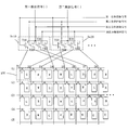
- FIG. 1 is a multiplexed display driving circuit used in a conventional display device using an RGBW four-color pixel structure, comprising: a plurality of driving units, each of which includes: eight parallel and sequentially Arranged vertical data lines D1-D8, at least two horizontal scanning lines Gn (n is a positive integer) arranged in parallel and sequentially arranged, and at least two rows and eight columns of sixteen sub-pixels 100 arranged in an array And the first and second multiplexing modules De10 and De20; each of the sub-pixels 100 is electrically connected to the scan line corresponding to the row of the sub-pixel 100 and the data line corresponding to the column of the sub-pixel 100;
- the circuit multiplexing modules each include four thin film transistors, and the gates of the four thin film transistors are electrically connected to the first shunt control signal Demux1, the second shunt control signal Demux2, the third shunt control signal Demux3, and the The four-way control signal Demux4 has a source electrically connected to the same data signal, and
- the first multiplexing module De10 includes: a first thin film transistor T10, a gate of the first thin film transistor T10 is electrically connected to the first shunt control signal Demux1, and a source is electrically connected to the first One
- the data signal Data10, the drain is electrically connected to the first data line D1;
- the second thin film transistor T20, the gate of the second thin film transistor T20 is electrically connected to the second shunt control signal Demux2, and the source is electrically connected to The first data signal Data10, the drain is electrically connected to the sixth data line D6;
- the third thin film transistor T30, the gate of the third thin film transistor T30 is electrically connected to the third shunt control signal Demux3, and the source is electrically Connected to the first data signal Data10, the drain is electrically connected to the seventh data line D7;
- the fourth thin film transistor T40, the gate of the fourth thin film transistor T40 is electrically connected to the fourth shunt control signal Demux4, the source Electrically connected to the first data signal
- the gate control signal Demux2 the source is electrically connected to the second data signal Data20, the drain is electrically connected to the second data line D2, and the seventh thin film transistor T70 is electrically connected to the gate of the seventh thin film transistor T70.
- the three-way control signal Demux3 is electrically connected to the second data signal Data20, the drain is electrically connected to the third data line D3, and the eighth thin film transistor T80 is electrically connected to the gate of the eighth thin film transistor T80.
- the fourth branch control signal Demux4 is electrically connected to the second data signal Data20, and the drain is electrically connected to the eighth data line D8.
- the first data signal Data10 is positive polarity
- the second data signal Data20 is negative polarity
- the scan line Gn is connected to the scan signal Gate
- the first, second, third, and fourth shunt control signals Demux1 The pulse period of Demux2, Demux3, and Demux4 is equal to 1/4 of the pulse period of the scan signal Gate.
- the pulse period of the scan signal Gate is also shortened, thereby continuously compressing the first, second, third, and fourth shunt control signals Demux1, Demux2, Demux3, During the pulse period of Demux4, the data switching time allocated to each sub-pixel is also reduced, resulting in insufficient sub-pixel charging rate, and the data signal entering the sub-pixel does not reach the level voltage.
- the present invention provides a multiplexed display driving circuit comprising: a plurality of driving units, each of which includes: twenty-four vertical data lines which are parallel to each other and are sequentially arranged, At least two horizontal scan lines parallel to each other and arranged in sequence, at least two rows of two Fourteen columns of a total of forty eight sub-pixels arranged in an array, and eight multiplexing modules;
- Each sub-pixel is electrically connected to a scan line corresponding to a row of the sub-pixel and a data line corresponding to the column where the sub-pixel is located;
- Each multiplexer module includes three thin film transistors, and the gates of the three thin film transistors are electrically connected to the first shunt control signal, the second shunt control signal, and the third shunt control signal, respectively.
- the poles are electrically connected to the same data signal, and the drains are electrically connected to a data line respectively;
- the first multiplexing module includes: a first thin film transistor, a gate of the first thin film transistor is electrically connected to the first shunt control signal, and a source is electrically connected to the first data signal, and the drain is electrically Connected to the first data line; the second thin film transistor, the gate of the second thin film transistor is electrically connected to the second shunt control signal, the source is electrically connected to the first data signal, and the drain is electrically connected to the drain a fourth data line; and a third thin film transistor, the gate of the third thin film transistor is electrically connected to the third shunt control signal, the source is electrically connected to the first data signal, and the drain is electrically connected to the sixth Data line
- the second multiplexing module includes: a fourth thin film transistor, the gate of the fourth thin film transistor is electrically connected to the first shunt control signal, the source is electrically connected to the second data signal, and the drain is electrically connected a second thin film transistor, a gate of the fifth thin film transistor is electrically connected to the second shunt control signal, a source is electrically connected to the second data signal, and a drain is electrically connected to the third a data line; and a sixth thin film transistor, the gate of the sixth thin film transistor is electrically connected to the third shunt control signal, the source is electrically connected to the second data signal, and the drain is electrically connected to the fifth data line ;
- the third multiplexing module includes: a seventh thin film transistor, the gate of the seventh thin film transistor is electrically connected to the first shunt control signal, the source is electrically connected to the third data signal, and the drain is electrically connected
- the seventh thin film transistor, the gate of the eighth thin film transistor is electrically connected to the second shunt control signal, the source is electrically connected to the third data signal, and the drain is electrically connected to the ninth a data line; and a ninth thin film transistor, the gate of the ninth thin film transistor is electrically connected to the third shunt control signal, the source is electrically connected to the third data signal, and the drain is electrically connected to the twelfth data line;
- the fourth multiplexing module includes: a tenth thin film transistor, the gate of the tenth thin film transistor is electrically connected to the first shunt control signal, the source is electrically connected to the fourth data signal, and the drain is electrically connected The eighth data line; the eleventh thin film transistor, the gate of the eleventh thin film transistor is electrically connected to the second shunt control signal, the source is electrically connected to the fourth data signal, and the drain is electrically connected to a tenth data line; and a twelfth thin film transistor, the gate of the twelfth thin film transistor is electrically connected to the third shunt control signal, the source is electrically connected to the fourth data signal, and the drain is electrically connected to Eleventh data line;
- the fifth multiplexing module includes: a thirteenth thin film transistor, the gate of the thirteenth thin film transistor is electrically connected to the first shunt control signal, the source is electrically connected to the fifth data signal, and the drain is electrically Connected to the fourteenth data line; the fourteenth thin film transistor, the gate of the fourteenth thin film transistor is electrically connected to the second shunt control signal, the source is electrically connected to the fifth data signal, and the drain is electrically Connected to the fifteenth data line; and the fifteenth thin film transistor, the gate of the fifteenth thin film transistor is electrically connected to the third shunt control signal, and the source is electrically connected to the fifth data signal, and the drain Electrically connected to the seventeenth data line;
- the sixth multiplexing module includes: a sixteenth thin film transistor, the gate of the sixteenth thin film transistor is electrically connected to the first shunt control signal, and the source is electrically connected to the sixth data signal, and the drain is electrically Connected to the thirteenth data line; the seventeenth thin film transistor, the gate of the seventeenth thin film transistor is electrically connected to the second shunt control signal, and the source is electrically connected to the sixth data signal, and the drain is electrically connected Connected to the sixteenth data line; and the eighteenth thin film transistor, the gate of the eighteenth thin film transistor is electrically connected to the third shunt control signal, and the source is electrically connected to the sixth data signal, and the drain Electrically connected to the eighteenth data line;
- the seventh multiplexing module includes: a nineteenth thin film transistor, the gate of the nineteenth thin film transistor is electrically connected to the first shunt control signal, and the source is electrically connected to the seventh data signal, and the drain is electrically Connected to the twentieth data line; the twentieth thin film transistor, the gate of the twentieth thin film transistor is electrically connected to the second shunt control signal, and the source is electrically connected to the seventh data signal, and the drain is electrically The second eleventh thin film transistor is electrically connected to the third shunt control signal, and the source is electrically connected to the seventh data signal. The drain is electrically connected to the twenty-third data line;
- the eighth multiplexing module includes: a twenty-second thin film transistor, the gate of the twenty-second thin film transistor is electrically connected to the first shunt control signal, and the source is electrically connected to the eighth data signal, and the drain is electrically connected Electrode is electrically connected to the nineteenth data line; the twenty-third thin film transistor, the gate of the twenty-third thin film transistor is electrically connected to the second shunt control signal, and the source is electrically connected to the eighth data signal a drain electrically connected to the XXth data line; and a twenty-fourth thin film transistor, the gate of the twenty-fourth thin film transistor is electrically connected to the third shunt control signal, and the source is electrically connected An eighth data signal, the drain is electrically connected to the twenty-fourth data line;
- the adjacent two data signals have opposite polarities.
- Each sub-pixel is composed of a thin film transistor and a pixel electrode; the gate of the thin film transistor is electrically connected to the scan line corresponding to the row of the sub-pixel, and the source is electrically connected to the data line corresponding to the column of the sub-pixel. The drain is electrically connected to the pixel electrode.
- the sub-pixel includes: a red sub-pixel, a green sub-pixel, a blue sub-pixel, and a white sub-pixel; a red sub-pixel, a green sub-pixel, a blue sub-pixel, and a white sub-pixel The same constitutes a display pixel.
- the same column of sub-pixels have the same polarity; in the same row of display pixels, the polarity of the sub-pixels of the same color of the adjacent two columns of display pixels is different; in the same column of display pixels, the adjacent two rows display the same color of the pixels
- the sub-pixels have different polarities.
- the green sub-pixel, the blue sub-pixel, the red sub-pixel, and the white sub-pixel are sequentially arranged; in the second row of sub-display pixels, the red sub-pixel, the white sub-pixel, the green sub-pixel, and The blue sub-pixels are sequentially arranged; in the third row of display pixels, the green sub-pixel, the red sub-pixel, the blue sub-pixel, and the white sub-pixel are sequentially arranged; in the fourth row of sub-display pixels, the blue sub-pixel, white The sub-pixel, the green sub-pixel, and the red sub-pixel are sequentially arranged.
- the scan line is connected to the scan signal.
- the pulse periods of the first, second, and third shunt control signals are equal to 1/3 of the pulse period of the scan signal.
- a rising edge of the first shunt control signal is generated simultaneously with a rising edge of the scan signal during a pulse period of a scan signal, a rising edge of the second shunt control signal and the first shunt control a falling edge of the signal is simultaneously generated, a rising edge of the third shunt control signal is generated simultaneously with a falling edge of the second shunt control signal, a falling edge of the third shunt control signal and the scan signal The falling edge is generated at the same time.
- the first, third, fifth, and seventh data signals are all positive polarity
- the second, fourth, sixth, and eighth data signals are all negative polarity
- the polarities of the first to third column sub-pixels are positive, negative, and negative, respectively; the polarities of the fourth to sixth column sub-pixels are positive, negative, and positive, respectively; and the polarities of the seventh to ninth column sub-pixels are positive, respectively.
- the polarities of the tenth to twelfth column sub-pixels are negative, negative, and positive respectively; the polarities of the thirteenth to fifteenth column sub-pixels are negative, positive, and positive, respectively; sixteenth to eighteenth
- the polarity of the column sub-pixels are negative, positive and negative respectively; the polarities of the nineteenth to twenty-first column sub-pixels are negative, positive and negative, respectively; the polarities of the twenty-second to twenty-fourth column sub-pixels are respectively Positive, positive, negative.
- the present invention also provides a multiplexed display driving circuit comprising: a plurality of driving units, each driving unit comprising: twenty-four parallel data lines arranged in parallel and sequentially arranged, at least two parallel to each other And horizontally arranged horizontal scanning lines, at least two rows and twenty four columns, a total of forty eight sub-pixels arranged in an array, and eight multiplexing modules;
- Each sub-pixel is electrically connected to a scan line corresponding to a row of the sub-pixel and a data line corresponding to the column where the sub-pixel is located;
- Each multiplexer module includes three thin film transistors, and the gates of the three thin film transistors are electrically connected to the first shunt control signal, the second shunt control signal, and the third shunt control signal, respectively.
- the poles are electrically connected to the same data signal, and the drains are electrically connected to a data line respectively;
- the first multiplexing module includes: a first thin film transistor, a gate of the first thin film transistor is electrically connected to the first shunt control signal, and a source is electrically connected to the first data signal, and the drain is electrically Connected to the first data line; the second thin film transistor, the gate of the second thin film transistor is electrically connected to the second shunt control signal, the source is electrically connected to the first data signal, and the drain is electrically connected to the drain a fourth data line; and a third thin film transistor, the gate of the third thin film transistor is electrically connected to the third shunt control signal, the source is electrically connected to the first data signal, and the drain is electrically connected to the sixth Data line
- the second multiplexing module includes: a fourth thin film transistor, the gate of the fourth thin film transistor is electrically connected to the first shunt control signal, the source is electrically connected to the second data signal, and the drain is electrically connected a second thin film transistor, a gate of the fifth thin film transistor is electrically connected to the second shunt control signal, a source is electrically connected to the second data signal, and a drain is electrically connected to the third a data line; and a sixth thin film transistor, the gate of the sixth thin film transistor is electrically connected to the third shunt control signal, the source is electrically connected to the second data signal, and the drain is electrically connected to the fifth data line ;
- the third multiplexing module includes: a seventh thin film transistor, the gate of the seventh thin film transistor is electrically connected to the first shunt control signal, the source is electrically connected to the third data signal, and the drain is electrically connected
- the seventh thin film transistor, the gate of the eighth thin film transistor is electrically connected to the second shunt control signal, the source is electrically connected to the third data signal, and the drain is electrically connected to the ninth a data line; and a ninth thin film transistor, the gate of the ninth thin film transistor is electrically connected to the third shunt control signal, the source is electrically connected to the third data signal, and the drain is electrically connected to the twelfth data line;
- the fourth multiplexing module includes: a tenth thin film transistor, the gate of the tenth thin film transistor is electrically connected to the first shunt control signal, the source is electrically connected to the fourth data signal, and the drain is electrically connected The eighth data line; the eleventh thin film transistor, the gate of the eleventh thin film transistor is electrically connected to the second shunt control signal, the source is electrically connected to the fourth data signal, and the drain is electrically connected to a tenth data line; and a twelfth thin film transistor, the gate of the twelfth thin film transistor is electrically connected to the third shunt control signal, the source is electrically connected to the fourth data signal, and the drain is electrically connected to Eleventh data line;
- the fifth multiplexing module includes: a thirteenth thin film transistor, the gate of the thirteenth thin film transistor is electrically connected to the first shunt control signal, the source is electrically connected to the fifth data signal, and the drain is electrically Connected to the fourteenth data line; the fourteenth thin film transistor, the gate of the fourteenth thin film transistor is electrically connected to the second shunt control signal, the source is electrically connected to the fifth data signal, and the drain is electrically Connected to the fifteenth data line; and the fifteenth thin film transistor, the gate of the fifteenth thin film transistor is electrically connected to the third shunt control signal, and the source is electrically connected to the fifth data signal, The drain is electrically connected to the seventeenth data line;
- the sixth multiplexing module includes: a sixteenth thin film transistor, the gate of the sixteenth thin film transistor is electrically connected to the first shunt control signal, and the source is electrically connected to the sixth data signal, and the drain is electrically Connected to the thirteenth data line; the seventeenth thin film transistor, the gate of the seventeenth thin film transistor is electrically connected to the second shunt control signal, and the source is electrically connected to the sixth data signal, and the drain is electrically connected Connected to the sixteenth data line; and the eighteenth thin film transistor, the gate of the eighteenth thin film transistor is electrically connected to the third shunt control signal, and the source is electrically connected to the sixth data signal, and the drain Electrically connected to the eighteenth data line;
- the seventh multiplexing module includes: a nineteenth thin film transistor, the gate of the nineteenth thin film transistor is electrically connected to the first shunt control signal, and the source is electrically connected to the seventh data signal, and the drain is electrically Connected to the twentieth data line; the twentieth thin film transistor, the gate of the twentieth thin film transistor is electrically connected to the second shunt control signal, and the source is electrically connected to the seventh data signal, and the drain is electrically The second eleventh thin film transistor is electrically connected to the third shunt control signal, and the source is electrically connected to the seventh data signal. The drain is electrically connected to the twenty-third data line;
- the eighth multiplexing module includes: a twenty-second thin film transistor, the gate of the twenty-second thin film transistor is electrically connected to the first shunt control signal, and the source is electrically connected to the eighth data signal, and the drain is electrically connected Electrode is electrically connected to the nineteenth data line; the twenty-third thin film transistor, the gate of the twenty-third thin film transistor is electrically connected to the second shunt control signal, and the source is electrically connected to the eighth data signal a drain electrically connected to the XXth data line; and a twenty-fourth thin film transistor, the gate of the twenty-fourth thin film transistor is electrically connected to the third shunt control signal, and the source is electrically connected An eighth data signal, the drain is electrically connected to the twenty-fourth data line;
- the adjacent two data signals have opposite polarities
- Each sub-pixel is composed of a thin film transistor and a pixel electrode; a gate of the thin film transistor is electrically connected to a scan line corresponding to a row of the sub-pixel, and a source is electrically connected to a column corresponding to the sub-pixel. a data line, the drain is electrically connected to the pixel electrode;
- the sub-pixel includes: a red sub-pixel, a green sub-pixel, a blue sub-pixel, and a white sub-pixel; a red sub-pixel, a green sub-pixel, a blue sub-pixel, and a white sub-pixel together form a Display pixel
- the scan line is connected to the scan signal
- the first, third, fifth, and seventh data signals are all positive polarity, and the second, fourth, sixth, and eighth data signals are all negative polarity.
- the present invention provides a multiplexed display driving circuit suitable for a high-resolution display device using an RGBW four-color pixel structure, which is provided with a plurality of driving
- Each of the driving units is provided with eight multiplexing modules, each of which includes three thin film transistors, and the gates of the three thin film transistors are electrically connected to the first shunt control signal, respectively.
- the two-way control signal and the third shunt control signal, the source is electrically connected to the same data signal, and the drain is electrically connected to a data line by a jumper, so that the pulse period of each shunt control signal can be made. It is equal to 1/3 of the scanning signal period, so that the charging time of the data signal is increased and the charging rate of the sub-pixel is increased without changing the scanning signal pulse period.
- FIG. 1 is a schematic diagram of a multiplexed display driving circuit used in a conventional display device using an RGBW four-color pixel structure
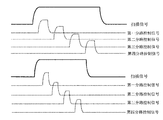
- FIG. 2 is a comparison diagram of the shunt control signals of the display driving circuit shown in FIG. 1 at different resolutions;
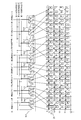
- FIG. 3 is a schematic diagram of a multiplex type display driving circuit of the present invention.
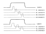
- FIG. 4 is a comparison diagram of the shunt control signals of the multiplexed display drive circuit of the present invention and the display drive circuit of FIG. 1 at the same high resolution.
- the present invention provides a multiplexed display driving circuit, including: a plurality of driving units, each of which includes: twenty-four vertical data lines D1- arranged in parallel and sequentially arranged. D24, at least two horizontal scanning lines Gn (n is a positive integer) arranged in parallel and sequentially, at least two rows and twenty four columns, a total of forty-eight sub-pixels 10 arranged in an array, and eight multiplexing Modules De1-De8.
- Each sub-pixel is electrically connected to a scan line corresponding to a row of the sub-pixel and a data line corresponding to the column where the sub-pixel is located;
- Each multiplexer module includes three thin film transistors, and the gates of the three thin film transistors are electrically connected to the first shunt control signal Demoux1, the second shunt control signal Demux2, and the third shunt control signal Demux3, respectively.
- the source is electrically connected to the same data signal, and the drain is electrically connected to a data line;
- the first multiplexing module De1 includes: a first thin film transistor T1, a gate of the first thin film transistor T1 is electrically connected to the first shunt control signal Demux1, and a source is electrically connected to the first The data signal Data1, the drain is electrically connected to the first data line D1; the second thin film transistor T2, the gate of the second thin film transistor T2 is electrically connected to the second shunt control signal Demux2, and the source is electrically connected to The first data signal Data1, the drain is electrically connected to the fourth data line D4; and the third thin film transistor T3, the gate of the third thin film transistor T3 is electrically connected to the third shunt control signal Demux3, and the source is electrically Connected to the first data signal Data1, the drain is electrically connected to the sixth data line D6;
- the second multiplexing module De2 includes a fourth thin film transistor T4, the gate of the fourth thin film transistor T4 is electrically connected to the first shunt control signal Demux1, and the source is electrically connected to the second data signal Data2.
- the drain is electrically connected to the second data line D2; the fifth thin film transistor T5, the gate of the fifth thin film transistor T5 is electrically connected to the second shunt control signal Demux2, and the source is electrically connected to the second data signal.
- the drain is electrically connected to the third data line D3; and the sixth thin film transistor T6, the gate of the sixth thin film transistor T6 is electrically connected to the third shunt control signal Demux3, and the source is electrically connected to the The second data signal Data2, the drain is electrically connected to the fifth data line D5;
- the third multiplexing module De3 includes a seventh thin film transistor T7, the gate of the seventh thin film transistor T7 is electrically connected to the first shunt control signal Demux1, and the source is electrically connected to the third data signal Data3.
- the drain is electrically connected to the seventh data line D7; the eighth thin film transistor T8, the gate of the eighth thin film transistor T8 is electrically connected to the second shunt control signal Demux2, and the source is electrically connected to the third data signal.
- the drain is electrically connected to the ninth data line D9; and the ninth thin film transistor T9, the gate of the ninth thin film transistor T9 is electrically connected to the third shunt control signal Demux3, and the source is electrically connected to the The third data signal Data3, the drain is electrically connected to the twelfth data line D12;
- the fourth multiplexing module De4 includes a tenth thin film transistor T10, the gate of the tenth thin film transistor T10 is electrically connected to the first shunt control signal Demux1, and the source is electrically connected to the fourth data signal Data4.
- the drain is electrically connected to the eighth data line D8; the eleventh thin film transistor T11, the gate of the eleventh thin film transistor T11 is electrically connected to the second shunt control signal Demux2, and the source is electrically connected to the fourth The data signal Data4, the drain is electrically connected to the tenth data line D10; and the twelfth thin film transistor T12, the gate of the twelfth thin film transistor T12 is electrically connected to the third shunt control signal Demux3, and the source is electrically Connected to the fourth data signal Data4, the drain is electrically connected to the eleventh data line D11;
- the fifth multiplexing module De5 includes: a thirteenth thin film transistor T13, the gate of the thirteenth thin film transistor T13 is electrically connected to the first shunt control signal Demux1, and the source is electrically connected.
- the drain is electrically connected to the fourteenth data line D14; the fourteenth thin film transistor T14, the gate of the fourteenth thin film transistor T14 is electrically connected to the second shunt control signal Demux2,
- the source is electrically connected to the fifth data signal Data5, the drain is electrically connected to the fifteenth data line D15; and the fifteenth thin film transistor T15, the gate of the fifteenth thin film transistor T15 is electrically connected to the third The shunt control signal Demux3, the source is electrically connected to the fifth data signal Data5, and the drain is electrically connected to the seventeenth data line D17;
- the sixth multiplexing module De6 includes: a sixteenth thin film transistor T16, the gate of the sixteenth thin film transistor T16 is electrically connected to the first shunt control signal Demux1, and the source is electrically connected to the sixth data signal. Data6, the drain is electrically connected to the thirteenth data line D13; the seventeenth thin film transistor T17, the gate of the seventeenth thin film transistor T17 is electrically connected to the second shunt control signal Demux2, and the source is electrically connected.
- the drain is electrically connected to the sixteenth data line D16; and the eighteenth thin film transistor T18, the gate of the eighteenth thin film transistor T18 is electrically connected to the third shunt control signal Demux3
- the source is electrically connected to the sixth data signal Data6, and the drain is electrically connected to the eighteenth data line D18;
- the seventh multiplexing module De7 includes: a nineteenth thin film transistor T19, the gate of the nineteenth thin film transistor T19 is electrically connected to the first shunt control signal Demux1, and the source is electrically connected to the seventh data signal.
- the gate of the twentieth thin film transistor T20 is electrically connected to the second shunt control signal Demux2, and the source is electrically connected.
- the seventh data signal Data7, the drain is electrically connected to the twenty-second data line D22; and the twenty-first thin film transistor T21, the gate of the twenty-first thin film transistor T21 is electrically connected to the third branch Control signal Demux3, the source is electrically connected to the seventh data signal Data7, the drain is electrically connected to the twenty-third data line D23;
- the eighth multiplexing module De8 includes: a twenty-second thin film transistor T22, the gate of the twenty-second thin film transistor T22 is electrically connected to the first shunt control signal Demux1, and the source is electrically connected to the eighth The data signal Data8, the drain is electrically connected to the nineteenth data line D19; the twenty-third thin film transistor T23, the gate of the twenty-third thin film transistor T23 is electrically connected to the second shunt control signal Demux2, the source The gate is electrically connected to the eighth data signal Data8, the drain is electrically connected to the second eleventh data line D21, and the twenty-fourth thin film transistor T24 is electrically connected to the gate of the twenty-fourth thin film transistor T24.
- the third shunt control signal Demux3 is electrically connected to the eighth data signal Data8, and the drain is electrically connected to the twenty-fourth data line D24.
- the polarity of the two adjacent data signals is opposite.
- the first, third, fifth, and seventh data signals Data1, Data3, Data5, and Data7 are all positive polarity
- the second, fourth, and fourth The sixth and eighth data signals Data2, Data4, Data6, and Data8 are both negative polarity
- the drains of the three thin film transistors in each multiplexing module are electrically connected to each other by the above jumper method.
- the data lines are such that the polarities of the first to third column sub-pixels 10 are positive, negative, and negative, respectively; the polarities of the fourth to sixth column sub-pixels 10 are positive, negative, and positive, respectively; and the seventh to ninth columns of sub-pixels 10
- the polarities of the tenth to twelfth columns of the sub-pixels 10 are negative, negative, and positive, respectively; and the polarities of the thirteenth to fifteenth column sub-pixels 10 are negative, positive, and respectively.
- the polarity of the sixteenth to eighteenth column sub-pixels 10 are negative, positive, and negative respectively; the polarities of the nineteenth to twenty-first column sub-pixels 10 are negative, positive, and negative, respectively; The polarities of the twenty-fourth column sub-pixel 10 are positive, positive, and negative, respectively.
- each sub-pixel 10 is composed of a thin film transistor T and a pixel electrode 20.
- the gate of the thin film transistor T is electrically connected to the scan line corresponding to the row of the sub-pixel 10
- the source is electrically connected to the data line corresponding to the column of the sub-pixel 10
- the drain is electrically connected to the pixel electrode. 20.
- the sub-pixel 10 includes: a red sub-pixel R, a green sub-pixel G, a blue sub-pixel B, and a white sub-pixel W; a red sub-pixel R, a green sub-pixel G, and a blue sub-pixel B And a white sub-pixel W together constitute a display pixel. As shown in FIG.
- the green sub-pixel G, the blue sub-pixel B, the red sub-pixel R, and the white sub-pixel W are sequentially arranged; in the second row of sub-display pixels, the red sub-pixel R, white sub-pixel W, green sub-pixel G, and blue sub-pixel B are sequentially arranged; in the third row of display pixels, green sub-pixel G, red sub-pixel R, blue sub-pixel B, and white sub-pixel W In the fourth row of sub-display pixels, the blue sub-pixel B, the white sub-pixel W, the green sub-pixel G, and the red sub-pixel R are sequentially arranged.
- Such a sub-pixel arrangement manner is matched with the wiring manner of each of the multiplex modules described above such that the same column sub-pixels 10 have the same polarity; in the same row of display pixels, the adjacent two columns display pixels of the same color of the sub-pixels The polarity is different; in the same column of display pixels, the polarity of the sub-pixels of the same color of the adjacent two rows of display pixels is different.
- the positive and negative polarities of the sub-pixels of the same color cancel out, which avoids picture crosstalk and ensures display quality.
- the scan line is connected to a scan signal Gate, the scan signal Gate is provided by a gate driver, and the data signal is provided by a source driver.
- the pulse periods of the first, second, and third shunt control signals Demux1, Demux2, and Demux3 are equal to 1/3 of the pulse period of the scan signal Gate.
- a rising edge of the first shunt control signal Demux1 is generated simultaneously with a rising edge of the scan signal Gate, and a rising edge of the second shunt control signal Demux2 and the first A falling edge of a shunt control signal Demux1 is simultaneously generated, and a rising edge of the third shunt control signal Demux3 is simultaneously generated with a falling edge of the second shunt control signal Demux2, the third shunt control signal Demux3
- the falling edge is generated simultaneously with the falling edge of the scan signal Gate.
- the multiplexed display driving circuit of the present invention sets three shunt control signals under the same short scan signal Gate pulse period, and the pulse period of each shunt control signal is compared with the prior art.
- the opening time of each column of sub-pixels 10 is extended, so that the charging time of the data signal can be increased without changing the pulse period of the scan signal, and the sub-pixel can be raised. 10 charge rate.
- the multiplexed display driving circuit of the present invention is suitable for a high-resolution display device using an RGBW four-color pixel structure, which is provided with a plurality of driving units, and each driving unit is provided with eight multi-channels.
- a multiplexing module each of the multiplexing modules includes three thin film transistors, and the gates of the three thin film transistors are electrically connected to the first shunt control signal, the second shunt control signal, and the third shunt, respectively
- the control signal, the source is electrically connected to the same data signal, and the drain is electrically connected to a data line by a jumper, so that the pulse period of each shunt control signal is equal to 1/3 of the scan signal period, thereby When the scanning signal pulse period is not changed, the charging time of the data signal is increased, and the charging rate of the sub-pixel is increased.
Landscapes
- Engineering & Computer Science (AREA)
- Chemical & Material Sciences (AREA)
- Crystallography & Structural Chemistry (AREA)
- Physics & Mathematics (AREA)
- Computer Hardware Design (AREA)
- General Physics & Mathematics (AREA)
- Theoretical Computer Science (AREA)
- Control Of Indicators Other Than Cathode Ray Tubes (AREA)
Abstract
提供一种多路复用型显示驱动电路,适用于高解析度的RGBW四色像素结构的显示装置,其装置设置有多个驱动单元,每个驱动单元设置有八个多路复用模块(De1, De2, De3, De4, De5 De6, De7, De8),每一多路复用模块均包括三个薄膜晶体管(T1,…T24),该三个薄膜晶体管(T1,…T24)的栅极分别电性连接于第一分路控制信号(Demux1)、第二分路控制信号(Demux2)、第三分路控制信号(Demux3)、源极均电性连接同一数据信号(Data1,…Data8),漏极以跳线方式分别电性连接一数据线(D1,…D24),使得每一分路控制信号(Demux1,Demux2,Demux3)的脉冲周期等于扫描周期的1/3,从而在不改变扫描信号脉冲周期的情况下,增加数据信号的充电时间,提升子像素(R、G、B、W)的充电率。
Description
本发明涉及显示技术领域,尤其涉及一种多路复用型显示驱动电路。
在液晶显示装置(Liquid Crystal Display,LCD)与有机发光二极管显示装置(Organic Light Emitting Display,OLED)等平板显示装置中均包括多个阵列式排布的像素,每个像素通常包括红、绿、蓝三种颜色的子像素,每个子像素均受控于一条栅极线与一条数据线,栅极线用于控制子像素的开启和关闭,数据线通过向子像素施加不同的数据电压信号,使子像素显示不同的灰阶,从而实现全彩画面的显示。
随着显示技术的发展,人们对显示装置的显示亮度、色彩还原性、画面色彩的丰富性等显示品质的追求越来越高,仅利用红色、绿色和蓝色三基色的显示装置,已不能满足人们对显示装置的需求。随之提出了一种由红、绿、蓝、白四种颜色组成的四色显示装置,在每个像素中增加一白色子像素,形成由红色子像素R、绿色子像素G、蓝色子像素B、及白色子像素W构成的RGBW像素结构。采用RGBW像素结构的显示装置在同样的显示画面下,比采用RGB三色子像素结构的显示装置具有更大的像素间距(pixel pitch),且增加的白色子像素具有高穿透率,使得采用RGBW四色像素结构的显示装置具有高穿透率和高开口率的优点,受到消费者的追捧。
图1所示为一种现有的采用RGBW四色像素结构的显示装置所使用的多路复用型显示驱动电路,包括:多个驱动单元,每一驱动单元均包括:八条相互平行并依次排列的竖直的数据线D1-D8、至少两条相互平行并依次排列的水平的扫描线Gn(n为正整数)、至少二行八列共十六个呈阵列式排布的子像素100、以及第一和第二多路复用模块De10、De20;每一子像素100电性连接于该子像素100所在行对应的扫描线和该子像素100所在列对应的数据线;每一多路复用模块均包括四个薄膜晶体管,该四个薄膜晶体管的栅极分别电性连接于第一分路控制信号Demux1、第二分路控制信号Demux2、第三分路控制信号Demux3、和第四分路控制信号Demux4,源极均电性连接同一数据信号,漏极分别电性连接一数据线。具体地,所述第一多路复用模块De10包括:第一薄膜晶体管T10,所述第一薄膜晶体管T10的栅极电性连接于第一分路控制信号Demux1,源极电性连接于第一
数据信号Data10,漏极电性连接于第一数据线D1;第二薄膜晶体管T20,所述第二薄膜晶体管T20的栅极电性连接于第二分路控制信号Demux2,源极电性连接于第一数据信号Data10,漏极电性连接于第六数据线D6;第三薄膜晶体管T30,所述第三薄膜晶体管T30的栅极电性连接于第三分路控制信号Demux3,源极电性连接于第一数据信号Data10,漏极电性连接于第七数据线D7;第四薄膜晶体管T40,所述第四薄膜晶体管T40的栅极电性连接于第四分路控制信号Demux4,源极电性连接于第一数据信号Data10,漏极电性连接于第四数据线D4;第二多路复用模块De20包括:第五薄膜晶体管T50,所述第五薄膜晶体管T50的栅极电性连接于第一分路控制信号Demux1,源极电性连接于第二数据信号Data20,漏极电性连接于第五数据线D5;第六薄膜晶体管T60,所述第六薄膜晶体管T60的栅极电性连接于第二分路控制信号Demux2,源极电性连接于第二数据信号Data20,漏极电性连接于第二数据线D2;第七薄膜晶体管T70,所述第七薄膜晶体管T70的栅极电性连接于第三分路控制信号Demux3,源极电性连接于第二数据信号Data20,漏极电性连接于第三数据线D3;第八薄膜晶体管T80,所述第八薄膜晶体管T80的栅极电性连接于第四分路控制信号Demux4,源极电性连接于第二数据信号Data20,漏极电性连接于第八数据线D8。所述第一数据信号Data10为正极性,第二数据信号Data20为负极性,所述扫描线Gn接入扫描信号Gate,所述第一、第二、第三、和第四分路控制信号Demux1、Demux2、Demux3、Demux4的脉冲周期等于扫描信号Gate的脉冲周期的1/4。
请参阅图2,随着显示装置的解析度不断提高,扫描信号Gate的脉冲周期也不断缩短,从而不断压缩第一、第二、第三、和第四分路控制信号Demux1、Demux2、Demux3、Demux4的脉冲周期,每列子像素分配到的数据开关时间也随之缩小,导致子像素的充电率不足,进入子像素的数据信号达不到位准电压。
发明内容
本发明的目的在于提供一种多路复用型显示驱动电路,适用于高解析度的显示装置,能够在不改变扫描信号脉冲周期的情况下,增加数据信号的充电时间,提升子像素的充电率。
为实现上述目的,本发明提供了一种多路复用型显示驱动电路,包括:多个驱动单元,每一驱动单元均包括:二十四条相互平行并依次排列的竖直的数据线、至少两条相互平行并依次排列的水平的扫描线、至少二行二
十四列共四十八个呈阵列式排布的子像素、以及八个多路复用模块;
每一子像素电性连接于该子像素所在行对应的扫描线和该子像素所在列对应的数据线;
每一多路复用模块均包括三个薄膜晶体管,该三个薄膜晶体管的栅极分别电性连接于第一分路控制信号、第二分路控制信号、和第三分路控制信号,源极均电性连接同一数据信号,漏极分别电性连接一数据线;
所述第一多路复用模块包括:第一薄膜晶体管,所述第一薄膜晶体管的栅极电性连接于第一分路控制信号,源极电性连接于第一数据信号,漏极电性连接于第一数据线;第二薄膜晶体管,所述第二薄膜晶体管的栅极电性连接于第二分路控制信号,源极电性连接于第一数据信号,漏极电性连接于第四数据线;以及第三薄膜晶体管,所述第三薄膜晶体管的栅极电性连接于第三分路控制信号,源极电性连接于第一数据信号,漏极电性连接于第六数据线;
第二多路复用模块包括:第四薄膜晶体管,所述第四薄膜晶体管的栅极电性连接于第一分路控制信号,源极电性连接于第二数据信号,漏极电性连接于第二数据线;第五薄膜晶体管,所述第五薄膜晶体管的栅极电性连接于第二分路控制信号,源极电性连接于第二数据信号,漏极电性连接于第三数据线;以及第六薄膜晶体管,所述第六薄膜晶体管的栅极电性连接于第三分路控制信号,源极电性连接于第二数据信号,漏极电性连接于第五数据线;
第三多路复用模块包括:第七薄膜晶体管,所述第七薄膜晶体管的栅极电性连接于第一分路控制信号,源极电性连接于第三数据信号,漏极电性连接于第七数据线;第八薄膜晶体管,所述第八薄膜晶体管的栅极电性连接于第二分路控制信号,源极电性连接于第三数据信号,漏极电性连接于第九数据线;以及第九薄膜晶体管,所述第九薄膜晶体管的栅极电性连接于第三分路控制信号,源极电性连接于第三数据信号,漏极电性连接于第十二数据线;
第四多路复用模块包括:第十薄膜晶体管,所述第十薄膜晶体管的栅极电性连接于第一分路控制信号,源极电性连接于第四数据信号,漏极电性连接于第八数据线;第十一薄膜晶体管,所述第十一薄膜晶体管的栅极电性连接于第二分路控制信号,源极电性连接于第四数据信号,漏极电性连接于第十数据线;以及第十二薄膜晶体管,所述第十二薄膜晶体管的栅极电性连接于第三分路控制信号,源极电性连接于第四数据信号,漏极电性连接于第十一数据线;
第五多路复用模块包括:第十三薄膜晶体管,所述第十三薄膜晶体管的栅极电性连接于第一分路控制信号,源极电性连接于第五数据信号,漏极电性连接于第十四数据线;第十四薄膜晶体管,所述第十四薄膜晶体管的栅极电性连接于第二分路控制信号,源极电性连接于第五数据信号,漏极电性连接于第十五数据线;以及第十五薄膜晶体管,所述第十五薄膜晶体管的栅极电性连接于第三分路控制信号,源极电性连接于第五数据信号,漏极电性连接于第十七数据线;
第六多路复用模块包括:第十六薄膜晶体管,所述第十六薄膜晶体管的栅极电性连接于第一分路控制信号,源极电性连接于第六数据信号,漏极电性连接于第十三数据线;第十七薄膜晶体管,所述第十七薄膜晶体管的栅极电性连接于第二分路控制信号,源极电性连接于第六数据信号,漏极电性连接于第十六数据线;以及第十八薄膜晶体管,所述第十八薄膜晶体管的栅极电性连接于第三分路控制信号,源极电性连接于第六数据信号,漏极电性连接于第十八数据线;
第七多路复用模块包括:第十九薄膜晶体管,所述第十九薄膜晶体管的栅极电性连接于第一分路控制信号,源极电性连接于第七数据信号,漏极电性连接于第二十数据线;第二十薄膜晶体管,所述第二十薄膜晶体管的栅极电性连接于第二分路控制信号,源极电性连接于第七数据信号,漏极电性连接于第二十二数据线;以及第二十一薄膜晶体管,所述第二十一薄膜晶体管的栅极电性连接于第三分路控制信号,源极电性连接于第七数据信号,漏极电性连接于第二十三数据线;
第八多路复用模块包括:第二十二薄膜晶体管,所述第二十二薄膜晶体管的栅极电性连接于第一分路控制信号,源极电性连接于第八数据信号,漏极电性连接于第十九数据线;第二十三薄膜晶体管,所述第二十三薄膜晶体管的栅极电性连接于第二分路控制信号,源极电性连接于第八数据信号,漏极电性连接于第二十一数据线;以及第二十四薄膜晶体管,所述第二十四薄膜晶体管的栅极电性连接于第三分路控制信号,源极电性连接于第八数据信号,漏极电性连接于第二十四数据线;
相邻两条数据信号的极性相反。
每一子像素由一薄膜晶体管以及一像素电极构成;所述薄膜晶体管的栅极电性连接于该子像素所在行对应的扫描线,源极电性连接于该子像素所在列对应的数据线,漏极电性连接于所述像素电极。
所述子像素包括:红色子像素、绿色子像素、蓝色子像素、和白色子像素;一红色子像素、一绿色子像素、一蓝色子像素、和一白色子像素共
同构成一显示像素。
同一列子像素的极性相同;在同一行显示像素中,相邻两列显示像素的同种颜色的子像素的极性不同;在同一列显示像素中,相邻两行显示像素的同种颜色的子像素的极性不同。
在第一行显示像素中,绿色子像素、蓝色子像素、红色子像素、和白色子像素依次排列;在第二行子显示像素中,红色子像素、白色子像素、绿色子像素、和蓝色子像素依次排列;在第三行显示像素中,绿色子像素、红色子像素、蓝色子像素、和白色子像素依次排列;在第四行子显示像素中,蓝色子像素、白色子像素、绿色子像素、和红色子像素依次排列。
所述扫描线接入扫描信号。
所述第一、第二、和第三分路控制信号的脉冲周期等于扫描信号的脉冲周期的1/3。
在一个扫描信号的脉冲周期内,所述第一分路控制信号的上升沿与所述扫描信号的上升沿同时产生,所述第二分路控制信号的上升沿与所述第一分路控制信号的下降沿同时产生,所述第三分路控制信号的上升沿与所述第二分路控制信号的下降沿同时产生,所述第三分路控制信号的下降沿与所述扫描信号的下降沿同时产生。
优选的,所述第一、第三、第五、和第七数据信号均为正极性,所述第二、第四、第六、和第八数据信号均为负极性。
第一至第三列子像素的极性分别为正、负、负;第四至第六列子像素的极性分别为正、负、正;第七至第九列子像素的极性分别为正、负、正;第十至第十二列子像素的极性分别为负、负、正;第十三至第十五列子像素的极性分别为负、正、正;第十六至第十八列子像素的极性分别为负、正、负;第十九至第二十一列子像素的极性分别为负、正、负;第二十二至第二十四列子像素的极性分别为正、正、负。
本发明还提供一种多路复用型显示驱动电路,包括:多个驱动单元,每一驱动单元均包括:二十四条相互平行并依次排列的竖直的数据线、至少两条相互平行并依次排列的水平的扫描线、至少二行二十四列共四十八个呈阵列式排布的子像素、以及八个多路复用模块;
每一子像素电性连接于该子像素所在行对应的扫描线和该子像素所在列对应的数据线;
每一多路复用模块均包括三个薄膜晶体管,该三个薄膜晶体管的栅极分别电性连接于第一分路控制信号、第二分路控制信号、和第三分路控制信号,源极均电性连接同一数据信号,漏极分别电性连接一数据线;
所述第一多路复用模块包括:第一薄膜晶体管,所述第一薄膜晶体管的栅极电性连接于第一分路控制信号,源极电性连接于第一数据信号,漏极电性连接于第一数据线;第二薄膜晶体管,所述第二薄膜晶体管的栅极电性连接于第二分路控制信号,源极电性连接于第一数据信号,漏极电性连接于第四数据线;以及第三薄膜晶体管,所述第三薄膜晶体管的栅极电性连接于第三分路控制信号,源极电性连接于第一数据信号,漏极电性连接于第六数据线;
第二多路复用模块包括:第四薄膜晶体管,所述第四薄膜晶体管的栅极电性连接于第一分路控制信号,源极电性连接于第二数据信号,漏极电性连接于第二数据线;第五薄膜晶体管,所述第五薄膜晶体管的栅极电性连接于第二分路控制信号,源极电性连接于第二数据信号,漏极电性连接于第三数据线;以及第六薄膜晶体管,所述第六薄膜晶体管的栅极电性连接于第三分路控制信号,源极电性连接于第二数据信号,漏极电性连接于第五数据线;
第三多路复用模块包括:第七薄膜晶体管,所述第七薄膜晶体管的栅极电性连接于第一分路控制信号,源极电性连接于第三数据信号,漏极电性连接于第七数据线;第八薄膜晶体管,所述第八薄膜晶体管的栅极电性连接于第二分路控制信号,源极电性连接于第三数据信号,漏极电性连接于第九数据线;以及第九薄膜晶体管,所述第九薄膜晶体管的栅极电性连接于第三分路控制信号,源极电性连接于第三数据信号,漏极电性连接于第十二数据线;
第四多路复用模块包括:第十薄膜晶体管,所述第十薄膜晶体管的栅极电性连接于第一分路控制信号,源极电性连接于第四数据信号,漏极电性连接于第八数据线;第十一薄膜晶体管,所述第十一薄膜晶体管的栅极电性连接于第二分路控制信号,源极电性连接于第四数据信号,漏极电性连接于第十数据线;以及第十二薄膜晶体管,所述第十二薄膜晶体管的栅极电性连接于第三分路控制信号,源极电性连接于第四数据信号,漏极电性连接于第十一数据线;
第五多路复用模块包括:第十三薄膜晶体管,所述第十三薄膜晶体管的栅极电性连接于第一分路控制信号,源极电性连接于第五数据信号,漏极电性连接于第十四数据线;第十四薄膜晶体管,所述第十四薄膜晶体管的栅极电性连接于第二分路控制信号,源极电性连接于第五数据信号,漏极电性连接于第十五数据线;以及第十五薄膜晶体管,所述第十五薄膜晶体管的栅极电性连接于第三分路控制信号,源极电性连接于第五数据信号,
漏极电性连接于第十七数据线;
第六多路复用模块包括:第十六薄膜晶体管,所述第十六薄膜晶体管的栅极电性连接于第一分路控制信号,源极电性连接于第六数据信号,漏极电性连接于第十三数据线;第十七薄膜晶体管,所述第十七薄膜晶体管的栅极电性连接于第二分路控制信号,源极电性连接于第六数据信号,漏极电性连接于第十六数据线;以及第十八薄膜晶体管,所述第十八薄膜晶体管的栅极电性连接于第三分路控制信号,源极电性连接于第六数据信号,漏极电性连接于第十八数据线;
第七多路复用模块包括:第十九薄膜晶体管,所述第十九薄膜晶体管的栅极电性连接于第一分路控制信号,源极电性连接于第七数据信号,漏极电性连接于第二十数据线;第二十薄膜晶体管,所述第二十薄膜晶体管的栅极电性连接于第二分路控制信号,源极电性连接于第七数据信号,漏极电性连接于第二十二数据线;以及第二十一薄膜晶体管,所述第二十一薄膜晶体管的栅极电性连接于第三分路控制信号,源极电性连接于第七数据信号,漏极电性连接于第二十三数据线;
第八多路复用模块包括:第二十二薄膜晶体管,所述第二十二薄膜晶体管的栅极电性连接于第一分路控制信号,源极电性连接于第八数据信号,漏极电性连接于第十九数据线;第二十三薄膜晶体管,所述第二十三薄膜晶体管的栅极电性连接于第二分路控制信号,源极电性连接于第八数据信号,漏极电性连接于第二十一数据线;以及第二十四薄膜晶体管,所述第二十四薄膜晶体管的栅极电性连接于第三分路控制信号,源极电性连接于第八数据信号,漏极电性连接于第二十四数据线;
相邻两条数据信号的极性相反;
其中,每一子像素由一薄膜晶体管以及一像素电极构成;所述薄膜晶体管的栅极电性连接于该子像素所在行对应的扫描线,源极电性连接于该子像素所在列对应的数据线,漏极电性连接于所述像素电极;
其中,所述子像素包括:红色子像素、绿色子像素、蓝色子像素、和白色子像素;一红色子像素、一绿色子像素、一蓝色子像素、和一白色子像素共同构成一显示像素;
其中,所述扫描线接入扫描信号;
其中,所述第一、第三、第五、和第七数据信号均为正极性,所述第二、第四、第六、和第八数据信号均为负极性。
本发明的有益效果:本发明提供的一种多路复用型显示驱动电路,适用于高解析度的采用RGBW四色像素结构的显示装置,其设置有多个驱动
单元,每一驱动单元设置八个多路复用模块,每一多路复用模块均包括三个薄膜晶体管,该三个薄膜晶体管的栅极分别电性连接于第一分路控制信号、第二分路控制信号、和第三分路控制信号,源极均电性连接同一数据信号,漏极以跳线方式分别电性连接一数据线,这样能够使得每一分路控制信号的脉冲周期等于扫描信号周期的1/3,从而在不改变扫描信号脉冲周期的情况下,增加数据信号的充电时间,提升子像素的充电率。
为了能更进一步了解本发明的特征以及技术内容,请参阅以下有关本发明的详细说明与附图,然而附图仅提供参考与说明用,并非用来对本发明加以限制。
附图中,
图1为现有的采用RGBW四色像素结构的显示装置所使用的多路复用型显示驱动电路的示意图;
图2为图1所示的显示驱动电路在不同解析度下分路控制信号的对比图;
图3为本发明的多路复用型显示驱动电路的示意图;
图4为本发明的多路复用型显示驱动电路与图1所示的显示驱动电路在同一高解析度下分路控制信号的对比图。
为更进一步阐述本发明所采取的技术手段及其效果,以下结合本发明的优选实施例及其附图进行详细描述。
请参阅图3,本发明提供一种多路复用型显示驱动电路,包括:多个驱动单元,每一驱动单元均包括:二十四条相互平行并依次排列的竖直的数据线D1-D24、至少两条相互平行并依次排列的水平的扫描线Gn(n为正整数)、至少二行二十四列共四十八个呈阵列式排布的子像素10、以及八个多路复用模块De1-De8。
每一子像素电性连接于该子像素所在行对应的扫描线和该子像素所在列对应的数据线;
每一多路复用模块均包括三个薄膜晶体管,该三个薄膜晶体管的栅极分别电性连接于第一分路控制信号Demux1、第二分路控制信号Demux2、第三分路控制信号Demux3,源极均电性连接同一数据信号,漏极分别电性连接一数据线;
其中,所述第一多路复用模块De1包括:第一薄膜晶体管T1,所述第一薄膜晶体管T1的栅极电性连接于第一分路控制信号Demux1,源极电性连接于第一数据信号Data1,漏极电性连接于第一数据线D1;第二薄膜晶体管T2,所述第二薄膜晶体管T2的栅极电性连接于第二分路控制信号Demux2,源极电性连接于第一数据信号Data1,漏极电性连接于第四数据线D4;以及第三薄膜晶体管T3,所述第三薄膜晶体管T3的栅极电性连接于第三分路控制信号Demux3,源极电性连接于第一数据信号Data1,漏极电性连接于第六数据线D6;
第二多路复用模块De2包括:第四薄膜晶体管T4,所述第四薄膜晶体管T4的栅极电性连接于第一分路控制信号Demux1,源极电性连接于第二数据信号Data2,漏极电性连接于第二数据线D2;第五薄膜晶体管T5,所述第五薄膜晶体管T5的栅极电性连接于第二分路控制信号Demux2,源极电性连接于第二数据信号Data2,漏极电性连接于第三数据线D3;以及第六薄膜晶体管T6,所述第六薄膜晶体管T6的栅极电性连接于第三分路控制信号Demux3,源极电性连接于第二数据信号Data2,漏极电性连接于第五数据线D5;
第三多路复用模块De3包括:第七薄膜晶体管T7,所述第七薄膜晶体管T7的栅极电性连接于第一分路控制信号Demux1,源极电性连接于第三数据信号Data3,漏极电性连接于第七数据线D7;第八薄膜晶体管T8,所述第八薄膜晶体管T8的栅极电性连接于第二分路控制信号Demux2,源极电性连接于第三数据信号Data3,漏极电性连接于第九数据线D9;以及第九薄膜晶体管T9,所述第九薄膜晶体管T9的栅极电性连接于第三分路控制信号Demux3,源极电性连接于第三数据信号Data3,漏极电性连接于第十二数据线D12;
第四多路复用模块De4包括:第十薄膜晶体管T10,所述第十薄膜晶体管T10的栅极电性连接于第一分路控制信号Demux1,源极电性连接于第四数据信号Data4,漏极电性连接于第八数据线D8;第十一薄膜晶体管T11,所述第十一薄膜晶体管T11的栅极电性连接于第二分路控制信号Demux2,源极电性连接于第四数据信号Data4,漏极电性连接于第十数据线D10;以及第十二薄膜晶体管T12,所述第十二薄膜晶体管T12的栅极电性连接于第三分路控制信号Demux3,源极电性连接于第四数据信号Data4,漏极电性连接于第十一数据线D11;
第五多路复用模块De5包括:第十三薄膜晶体管T13,所述第十三薄膜晶体管T13的栅极电性连接于第一分路控制信号Demux1,源极电性连接
于第五数据信号Data5,漏极电性连接于第十四数据线D14;第十四薄膜晶体管T14,所述第十四薄膜晶体管T14的栅极电性连接于第二分路控制信号Demux2,源极电性连接于第五数据信号Data5,漏极电性连接于第十五数据线D15;以及第十五薄膜晶体管T15,所述第十五薄膜晶体管T15的栅极电性连接于第三分路控制信号Demux3,源极电性连接于第五数据信号Data5,漏极电性连接于第十七数据线D17;
第六多路复用模块De6包括:第十六薄膜晶体管T16,所述第十六薄膜晶体管T16的栅极电性连接于第一分路控制信号Demux1,源极电性连接于第六数据信号Data6,漏极电性连接于第十三数据线D13;第十七薄膜晶体管T17,所述第十七薄膜晶体管T17的栅极电性连接于第二分路控制信号Demux2,源极电性连接于第六数据信号Data6,漏极电性连接于第十六数据线D16;以及第十八薄膜晶体管T18,所述第十八薄膜晶体管T18的栅极电性连接于第三分路控制信号Demux3,源极电性连接于第六数据信号Data6,漏极电性连接于第十八数据线D18;
第七多路复用模块De7包括:第十九薄膜晶体管T19,所述第十九薄膜晶体管T19的栅极电性连接于第一分路控制信号Demux1,源极电性连接于第七数据信号Data7,漏极电性连接于第二十数据线D20;第二十薄膜晶体管T20,所述第二十薄膜晶体管T20的栅极电性连接于第二分路控制信号Demux2,源极电性连接于第七数据信号Data7,漏极电性连接于第二十二数据线D22;以及第二十一薄膜晶体管T21,所述第二十一薄膜晶体管T21的栅极电性连接于第三分路控制信号Demux3,源极电性连接于第七数据信号Data7,漏极电性连接于第二十三数据线D23;
第八多路复用模块De8包括:第二十二薄膜晶体管T22,所述第二十二薄膜晶体管T22的栅极电性连接于第一分路控制信号Demux1,源极电性连接于第八数据信号Data8,漏极电性连接于第十九数据线D19;第二十三薄膜晶体管T23,所述第二十三薄膜晶体管T23的栅极电性连接于第二分路控制信号Demux2,源极电性连接于第八数据信号Data8,漏极电性连接于第二十一数据线D21;以及第二十四薄膜晶体管T24,所述第二十四薄膜晶体管T24的栅极电性连接于第三分路控制信号Demux3,源极电性连接于第八数据信号Data8,漏极电性连接于第二十四数据线D24。
相邻两条数据信号的极性相反,优选的,所述第一、第三、第五、和第七数据信号Data1、Data3、Data5、Data7均为正极性,所述第二、第四、第六、和第八数据信号Data2、Data4、Data6、Data8均为负极性,由于每一多路复用模块内三个薄膜晶体管的漏极以上述跳线方式分别电性连接一
数据线,使得第一至第三列子像素10的极性分别为正、负、负;第四至第六列子像素10的极性分别为正、负、正;第七至第九列子像素10的极性分别为正、负、正;第十至第十二列子像素10的极性分别为负、负、正;第十三至第十五列子像素10的极性分别为负、正、正;第十六至第十八列子像素10的极性分别为负、正、负;第十九至第二十一列子像素10的极性分别为负、正、负;第二十二至第二十四列子像素10的极性分别为正、正、负。
具体地,每一子像素10由一薄膜晶体管T以及一像素电极20构成。所述薄膜晶体管T的栅极电性连接于该子像素10所在行对应的扫描线,源极电性连接于该子像素10所在列对应的数据线,漏极电性连接于所述像素电极20。
进一步地,所述子像素10包括:红色子像素R、绿色子像素G、蓝色子像素B、和白色子像素W;一红色子像素R、一绿色子像素G、一蓝色子像素B、和一白色子像素W共同构成一显示像素。如图3所示,在第一行显示像素中,绿色子像素G、蓝色子像素B、红色子像素R、和白色子像素W依次排列;在第二行子显示像素中,红色子像素R、白色子像素W、绿色子像素G、和蓝色子像素B依次排列;在第三行显示像素中,绿色子像素G、红色子像素R、蓝色子像素B、和白色子像素W依次排列;在第四行子显示像素中,蓝色子像素B、白色子像素W、绿色子像素G、和红色子像素R依次排列。这样的子像素排布方式搭配上述每一多路复用模块的布线方式使得同一列子像素10的极性相同;在同一行显示像素中,相邻两列显示像素的同种颜色的子像素的极性不同;在同一列显示像素中,相邻两行显示像素的同种颜色的子像素的极性不同。在纯色画面下,同种颜色的子像素的正、负极性相抵消,能够避免画面串扰,保证显示质量。
所述扫描线接入扫描信号Gate,所述扫描信号Gate由栅极驱动器提供,数据信号由源极驱动器提供。
特别地,请参阅图4,所述第一、第二、和第三分路控制信号Demux1、Demux2、Demux3的脉冲周期等于扫描信号Gate的脉冲周期的1/3。在一个扫描信号Gate的脉冲周期内,所述第一分路控制信号Demux1的上升沿与所述扫描信号Gate的上升沿同时产生,所述第二分路控制信号Demux2的上升沿与所述第一分路控制信号Demux1的下降沿同时产生,所述第三分路控制信号Demux3的上升沿与所述第二分路控制信号Demux2的下降沿同时产生,所述第三分路控制信号Demux3的下降沿与所述扫描信号Gate的下降沿同时产生。对于采用RGBW四色像素结构的显示装置以高解析度
显示时,在同一较短的扫描信号Gate脉冲周期下,本发明的多路复用型显示驱动电路设置三个分路控制信号,相比于现有技术,每一分路控制信号的脉冲周期由扫描信号脉冲周期的1/4提升至1/3,每一列子像素10的打开时间得以延长,从而能够在不改变扫描信号Gate脉冲周期的情况下,增加数据信号的充电时间,提升子像素10的充电率。
综上所述,本发明的多路复用型显示驱动电路,适用于高解析度的采用RGBW四色像素结构的显示装置,其设置有多个驱动单元,每一驱动单元设置八个多路复用模块,每一多路复用模块均包括三个薄膜晶体管,该三个薄膜晶体管的栅极分别电性连接于第一分路控制信号、第二分路控制信号、和第三分路控制信号,源极均电性连接同一数据信号,漏极以跳线方式分别电性连接一数据线,这样能够使得每一分路控制信号的脉冲周期等于扫描信号周期的1/3,从而在不改变扫描信号脉冲周期的情况下,增加数据信号的充电时间,提升子像素的充电率。
以上所述,对于本领域的普通技术人员来说,可以根据本发明的技术方案和技术构思作出其他各种相应的改变和变形,而所有这些改变和变形都应属于本发明权利要求的保护范围。
Claims (16)
- 一种多路复用型显示驱动电路,包括:多个驱动单元,每一驱动单元均包括:二十四条相互平行并依次排列的竖直的数据线、至少两条相互平行并依次排列的水平的扫描线、至少二行二十四列共四十八个呈阵列式排布的子像素、以及八个多路复用模块;每一子像素电性连接于该子像素所在行对应的扫描线和该子像素所在列对应的数据线;每一多路复用模块均包括三个薄膜晶体管,该三个薄膜晶体管的栅极分别电性连接于第一分路控制信号、第二分路控制信号、和第三分路控制信号,源极均电性连接同一数据信号,漏极分别电性连接一数据线;所述第一多路复用模块包括:第一薄膜晶体管,所述第一薄膜晶体管的栅极电性连接于第一分路控制信号,源极电性连接于第一数据信号,漏极电性连接于第一数据线;第二薄膜晶体管,所述第二薄膜晶体管的栅极电性连接于第二分路控制信号,源极电性连接于第一数据信号,漏极电性连接于第四数据线;以及第三薄膜晶体管,所述第三薄膜晶体管的栅极电性连接于第三分路控制信号,源极电性连接于第一数据信号,漏极电性连接于第六数据线;第二多路复用模块包括:第四薄膜晶体管,所述第四薄膜晶体管的栅极电性连接于第一分路控制信号,源极电性连接于第二数据信号,漏极电性连接于第二数据线;第五薄膜晶体管,所述第五薄膜晶体管的栅极电性连接于第二分路控制信号,源极电性连接于第二数据信号,漏极电性连接于第三数据线;以及第六薄膜晶体管,所述第六薄膜晶体管的栅极电性连接于第三分路控制信号,源极电性连接于第二数据信号,漏极电性连接于第五数据线;第三多路复用模块包括:第七薄膜晶体管,所述第七薄膜晶体管的栅极电性连接于第一分路控制信号,源极电性连接于第三数据信号,漏极电性连接于第七数据线;第八薄膜晶体管,所述第八薄膜晶体管的栅极电性连接于第二分路控制信号,源极电性连接于第三数据信号,漏极电性连接于第九数据线;以及第九薄膜晶体管,所述第九薄膜晶体管的栅极电性连接于第三分路控制信号,源极电性连接于第三数据信号,漏极电性连接于第十二数据线;第四多路复用模块包括:第十薄膜晶体管,所述第十薄膜晶体管的栅 极电性连接于第一分路控制信号,源极电性连接于第四数据信号,漏极电性连接于第八数据线;第十一薄膜晶体管,所述第十一薄膜晶体管的栅极电性连接于第二分路控制信号,源极电性连接于第四数据信号,漏极电性连接于第十数据线;以及第十二薄膜晶体管,所述第十二薄膜晶体管的栅极电性连接于第三分路控制信号,源极电性连接于第四数据信号,漏极电性连接于第十一数据线;第五多路复用模块包括:第十三薄膜晶体管,所述第十三薄膜晶体管的栅极电性连接于第一分路控制信号,源极电性连接于第五数据信号,漏极电性连接于第十四数据线;第十四薄膜晶体管,所述第十四薄膜晶体管的栅极电性连接于第二分路控制信号,源极电性连接于第五数据信号,漏极电性连接于第十五数据线;以及第十五薄膜晶体管,所述第十五薄膜晶体管的栅极电性连接于第三分路控制信号,源极电性连接于第五数据信号,漏极电性连接于第十七数据线;第六多路复用模块包括:第十六薄膜晶体管,所述第十六薄膜晶体管的栅极电性连接于第一分路控制信号,源极电性连接于第六数据信号,漏极电性连接于第十三数据线;第十七薄膜晶体管,所述第十七薄膜晶体管的栅极电性连接于第二分路控制信号,源极电性连接于第六数据信号,漏极电性连接于第十六数据线;以及第十八薄膜晶体管,所述第十八薄膜晶体管的栅极电性连接于第三分路控制信号,源极电性连接于第六数据信号,漏极电性连接于第十八数据线;第七多路复用模块包括:第十九薄膜晶体管,所述第十九薄膜晶体管的栅极电性连接于第一分路控制信号,源极电性连接于第七数据信号,漏极电性连接于第二十数据线;第二十薄膜晶体管,所述第二十薄膜晶体管的栅极电性连接于第二分路控制信号,源极电性连接于第七数据信号,漏极电性连接于第二十二数据线;以及第二十一薄膜晶体管,所述第二十一薄膜晶体管的栅极电性连接于第三分路控制信号,源极电性连接于第七数据信号,漏极电性连接于第二十三数据线;第八多路复用模块包括:第二十二薄膜晶体管,所述第二十二薄膜晶体管的栅极电性连接于第一分路控制信号,源极电性连接于第八数据信号,漏极电性连接于第十九数据线;第二十三薄膜晶体管,所述第二十三薄膜晶体管的栅极电性连接于第二分路控制信号,源极电性连接于第八数据信号,漏极电性连接于第二十一数据线;以及第二十四薄膜晶体管,所述第二十四薄膜晶体管的栅极电性连接于第三分路控制信号,源极电性连接于第八数据信号,漏极电性连接于第二十四数据线;相邻两条数据信号的极性相反。
- 如权利要求1所述的多路复用型显示驱动电路,其中,每一子像素由一薄膜晶体管以及一像素电极构成;所述薄膜晶体管的栅极电性连接于该子像素所在行对应的扫描线,源极电性连接于该子像素所在列对应的数据线,漏极电性连接于所述像素电极。
- 如权利要求1所述的多路复用型显示驱动电路,其中,所述子像素包括:红色子像素、绿色子像素、蓝色子像素、和白色子像素;一红色子像素、一绿色子像素、一蓝色子像素、和一白色子像素共同构成一显示像素。
- 如权利要求3所述的多路复用型显示驱动电路,其中,同一列子像素的极性相同;在同一行显示像素中,相邻两列显示像素的同种颜色的子像素的极性不同;在同一列显示像素中,相邻两行显示像素的同种颜色的子像素的极性不同。
- 如权利要求4所述的多路复用型显示驱动电路,其中,在第一行显示像素中,绿色子像素、蓝色子像素、红色子像素、和白色子像素依次排列;在第二行子显示像素中,红色子像素、白色子像素、绿色子像素、和蓝色子像素依次排列;在第三行显示像素中,绿色子像素、红色子像素、蓝色子像素、和白色子像素依次排列;在第四行子显示像素中,蓝色子像素、白色子像素、绿色子像素、和红色子像素依次排列。
- 如权利要求1所述的多路复用型显示驱动电路,其中,所述扫描线接入扫描信号。
- 如权利要求6所述的多路复用型显示驱动电路,其中,所述第一、第二、和第三分路控制信号的脉冲周期等于扫描信号的脉冲周期的1/3。
- 如权利要求7所述的多路复用型显示驱动电路,其中,在一个扫描信号的脉冲周期内,所述第一分路控制信号的上升沿与所述扫描信号的上升沿同时产生,所述第二分路控制信号的上升沿与所述第一分路控制信号的下降沿同时产生,所述第三分路控制信号的上升沿与所述第二分路控制信号的下降沿同时产生,所述第三分路控制信号的下降沿与所述扫描信号的下降沿同时产生。
- 如权利要求1所述的多路复用型显示驱动电路,其中,所述第一、第三、第五、和第七数据信号均为正极性,所述第二、第四、第六、和第八数据信号均为负极性。
- 如权利要求9所述的多路复用型显示驱动电路,其中,第一至第三列子像素的极性分别为正、负、负;第四至第六列子像素的极性分别为 正、负、正;第七至第九列子像素的极性分别为正、负、正;第十至第十二列子像素的极性分别为负、负、正;第十三至第十五列子像素的极性分别为负、正、正;第十六至第十八列子像素的极性分别为负、正、负;第十九至第二十一列子像素的极性分别为负、正、负;第二十二至第二十四列子像素的极性分别为正、正、负。
- 一种多路复用型显示驱动电路,包括:多个驱动单元,每一驱动单元均包括:二十四条相互平行并依次排列的竖直的数据线、至少两条相互平行并依次排列的水平的扫描线、至少二行二十四列共四十八个呈阵列式排布的子像素、以及八个多路复用模块;每一子像素电性连接于该子像素所在行对应的扫描线和该子像素所在列对应的数据线;每一多路复用模块均包括三个薄膜晶体管,该三个薄膜晶体管的栅极分别电性连接于第一分路控制信号、第二分路控制信号、和第三分路控制信号,源极均电性连接同一数据信号,漏极分别电性连接一数据线;所述第一多路复用模块包括:第一薄膜晶体管,所述第一薄膜晶体管的栅极电性连接于第一分路控制信号,源极电性连接于第一数据信号,漏极电性连接于第一数据线;第二薄膜晶体管,所述第二薄膜晶体管的栅极电性连接于第二分路控制信号,源极电性连接于第一数据信号,漏极电性连接于第四数据线;以及第三薄膜晶体管,所述第三薄膜晶体管的栅极电性连接于第三分路控制信号,源极电性连接于第一数据信号,漏极电性连接于第六数据线;第二多路复用模块包括:第四薄膜晶体管,所述第四薄膜晶体管的栅极电性连接于第一分路控制信号,源极电性连接于第二数据信号,漏极电性连接于第二数据线;第五薄膜晶体管,所述第五薄膜晶体管的栅极电性连接于第二分路控制信号,源极电性连接于第二数据信号,漏极电性连接于第三数据线;以及第六薄膜晶体管,所述第六薄膜晶体管的栅极电性连接于第三分路控制信号,源极电性连接于第二数据信号,漏极电性连接于第五数据线;第三多路复用模块包括:第七薄膜晶体管,所述第七薄膜晶体管的栅极电性连接于第一分路控制信号,源极电性连接于第三数据信号,漏极电性连接于第七数据线;第八薄膜晶体管,所述第八薄膜晶体管的栅极电性连接于第二分路控制信号,源极电性连接于第三数据信号,漏极电性连接于第九数据线;以及第九薄膜晶体管,所述第九薄膜晶体管的栅极电性连接于第三分路控制信号,源极电性连接于第三数据信号,漏极电性连接于 第十二数据线;第四多路复用模块包括:第十薄膜晶体管,所述第十薄膜晶体管的栅极电性连接于第一分路控制信号,源极电性连接于第四数据信号,漏极电性连接于第八数据线;第十一薄膜晶体管,所述第十一薄膜晶体管的栅极电性连接于第二分路控制信号,源极电性连接于第四数据信号,漏极电性连接于第十数据线;以及第十二薄膜晶体管,所述第十二薄膜晶体管的栅极电性连接于第三分路控制信号,源极电性连接于第四数据信号,漏极电性连接于第十一数据线;第五多路复用模块包括:第十三薄膜晶体管,所述第十三薄膜晶体管的栅极电性连接于第一分路控制信号,源极电性连接于第五数据信号,漏极电性连接于第十四数据线;第十四薄膜晶体管,所述第十四薄膜晶体管的栅极电性连接于第二分路控制信号,源极电性连接于第五数据信号,漏极电性连接于第十五数据线;以及第十五薄膜晶体管,所述第十五薄膜晶体管的栅极电性连接于第三分路控制信号,源极电性连接于第五数据信号,漏极电性连接于第十七数据线;第六多路复用模块包括:第十六薄膜晶体管,所述第十六薄膜晶体管的栅极电性连接于第一分路控制信号,源极电性连接于第六数据信号,漏极电性连接于第十三数据线;第十七薄膜晶体管,所述第十七薄膜晶体管的栅极电性连接于第二分路控制信号,源极电性连接于第六数据信号,漏极电性连接于第十六数据线;以及第十八薄膜晶体管,所述第十八薄膜晶体管的栅极电性连接于第三分路控制信号,源极电性连接于第六数据信号,漏极电性连接于第十八数据线;第七多路复用模块包括:第十九薄膜晶体管,所述第十九薄膜晶体管的栅极电性连接于第一分路控制信号,源极电性连接于第七数据信号,漏极电性连接于第二十数据线;第二十薄膜晶体管,所述第二十薄膜晶体管的栅极电性连接于第二分路控制信号,源极电性连接于第七数据信号,漏极电性连接于第二十二数据线;以及第二十一薄膜晶体管,所述第二十一薄膜晶体管的栅极电性连接于第三分路控制信号,源极电性连接于第七数据信号,漏极电性连接于第二十三数据线;第八多路复用模块包括:第二十二薄膜晶体管,所述第二十二薄膜晶体管的栅极电性连接于第一分路控制信号,源极电性连接于第八数据信号,漏极电性连接于第十九数据线;第二十三薄膜晶体管,所述第二十三薄膜晶体管的栅极电性连接于第二分路控制信号,源极电性连接于第八数据信号,漏极电性连接于第二十一数据线;以及第二十四薄膜晶体管,所述第 二十四薄膜晶体管的栅极电性连接于第三分路控制信号,源极电性连接于第八数据信号,漏极电性连接于第二十四数据线;相邻两条数据信号的极性相反;其中,每一子像素由一薄膜晶体管以及一像素电极构成;所述薄膜晶体管的栅极电性连接于该子像素所在行对应的扫描线,源极电性连接于该子像素所在列对应的数据线,漏极电性连接于所述像素电极;其中,所述子像素包括:红色子像素、绿色子像素、蓝色子像素、和白色子像素;一红色子像素、一绿色子像素、一蓝色子像素、和一白色子像素共同构成一显示像素;其中,所述扫描线接入扫描信号;其中,所述第一、第三、第五、和第七数据信号均为正极性,所述第二、第四、第六、和第八数据信号均为负极性。
- 如权利要求11所述的多路复用型显示驱动电路,其中,同一列子像素的极性相同;在同一行显示像素中,相邻两列显示像素的同种颜色的子像素的极性不同;在同一列显示像素中,相邻两行显示像素的同种颜色的子像素的极性不同。
- 如权利要求12所述的多路复用型显示驱动电路,其中,在第一行显示像素中,绿色子像素、蓝色子像素、红色子像素、和白色子像素依次排列;在第二行子显示像素中,红色子像素、白色子像素、绿色子像素、和蓝色子像素依次排列;在第三行显示像素中,绿色子像素、红色子像素、蓝色子像素、和白色子像素依次排列;在第四行子显示像素中,蓝色子像素、白色子像素、绿色子像素、和红色子像素依次排列。
- 如权利要求11所述的多路复用型显示驱动电路,其中,所述第一、第二、和第三分路控制信号的脉冲周期等于扫描信号的脉冲周期的1/3。
- 如权利要求14所述的多路复用型显示驱动电路,其中,在一个扫描信号的脉冲周期内,所述第一分路控制信号的上升沿与所述扫描信号的上升沿同时产生,所述第二分路控制信号的上升沿与所述第一分路控制信号的下降沿同时产生,所述第三分路控制信号的上升沿与所述第二分路控制信号的下降沿同时产生,所述第三分路控制信号的下降沿与所述扫描信号的下降沿同时产生。
- 如权利要求11所述的多路复用型显示驱动电路,其中,第一至第三列子像素的极性分别为正、负、负;第四至第六列子像素的极性分别为正、负、正;第七至第九列子像素的极性分别为正、负、正;第十至第十二列子像素的极性分别为负、负、正;第十三至第十五列子像素的极性分 别为负、正、正;第十六至第十八列子像素的极性分别为负、正、负;第十九至第二十一列子像素的极性分别为负、正、负;第二十二至第二十四列子像素的极性分别为正、正、负。
Priority Applications (1)
| Application Number | Priority Date | Filing Date | Title |
|---|---|---|---|
| US15/026,596 US10049638B2 (en) | 2016-01-04 | 2016-02-24 | Demultiplex type display driving circuit |
Applications Claiming Priority (2)
| Application Number | Priority Date | Filing Date | Title |
|---|---|---|---|
| CN201610003066.5 | 2016-01-04 | ||
| CN201610003066.5A CN105469765B (zh) | 2016-01-04 | 2016-01-04 | 多路复用型显示驱动电路 |
Publications (1)
| Publication Number | Publication Date |
|---|---|
| WO2017117847A1 true WO2017117847A1 (zh) | 2017-07-13 |
Family
ID=55607396
Family Applications (1)
| Application Number | Title | Priority Date | Filing Date |
|---|---|---|---|
| PCT/CN2016/074466 Ceased WO2017117847A1 (zh) | 2016-01-04 | 2016-02-24 | 多路复用型显示驱动电路 |
Country Status (3)
| Country | Link |
|---|---|
| US (1) | US10049638B2 (zh) |
| CN (1) | CN105469765B (zh) |
| WO (1) | WO2017117847A1 (zh) |
Cited By (1)
| Publication number | Priority date | Publication date | Assignee | Title |
|---|---|---|---|---|
| TWI831587B (zh) * | 2023-01-30 | 2024-02-01 | 友達光電股份有限公司 | 畫素陣列基板 |
Families Citing this family (39)
| Publication number | Priority date | Publication date | Assignee | Title |
|---|---|---|---|---|
| CN105810173B (zh) * | 2016-05-31 | 2018-08-14 | 武汉华星光电技术有限公司 | 多路复用型显示驱动电路 |
| CN105913823A (zh) * | 2016-06-23 | 2016-08-31 | 武汉华星光电技术有限公司 | 高解析度解复用器驱动电路 |
| CN105957484B (zh) * | 2016-07-01 | 2019-01-04 | 武汉华星光电技术有限公司 | 一种基于液晶面板的驱动电路及液晶面板 |
| CN106057164A (zh) | 2016-08-10 | 2016-10-26 | 武汉华星光电技术有限公司 | Rgbw四基色面板驱动架构 |
| CN106128388B (zh) * | 2016-08-29 | 2018-12-11 | 武汉华星光电技术有限公司 | 一种驱动电路及液晶显示面板 |
| CN106710502A (zh) * | 2016-12-26 | 2017-05-24 | 武汉华星光电技术有限公司 | 一种显示面板及用于驱动显示面板的多路复用驱动电路 |
| CN106782405B (zh) * | 2017-02-07 | 2019-04-30 | 武汉华星光电技术有限公司 | 显示驱动电路及液晶显示面板 |
| WO2018235130A1 (ja) * | 2017-06-19 | 2018-12-27 | シャープ株式会社 | 表示装置およびその駆動方法 |
| CN107393474B (zh) * | 2017-08-29 | 2019-09-10 | 深圳市华星光电半导体显示技术有限公司 | 透明双面显示装置及其驱动方法 |
| US10249247B2 (en) | 2017-08-29 | 2019-04-02 | Shenzhen China Star Optoelectronics Semiconductor Display Technology Co., Ltd. | Transparent dual-sided display device and driving method thereof |
| CN107632477B (zh) * | 2017-10-12 | 2024-06-28 | 惠科股份有限公司 | 阵列基板及其应用的显示面板 |
| KR102698364B1 (ko) | 2017-10-26 | 2024-08-23 | 매직 립, 인코포레이티드 | 증강 현실 디스플레이를 위한 광대역 적응형 렌즈 어셈블리 |
| CN108181770A (zh) * | 2018-02-11 | 2018-06-19 | 厦门天马微电子有限公司 | 一种显示面板及显示装置 |
| CN108333841B (zh) * | 2018-02-13 | 2021-04-09 | 厦门天马微电子有限公司 | 显示面板、显示装置及其驱动方法 |
| CN108198539A (zh) * | 2018-02-13 | 2018-06-22 | 厦门天马微电子有限公司 | 显示面板及其驱动方法、显示装置 |
| CN110176202B (zh) | 2018-04-16 | 2021-04-06 | 京东方科技集团股份有限公司 | 信号处理电路及其驱动方法、显示面板及显示装置 |
| CN108615504B (zh) * | 2018-05-10 | 2020-11-03 | 武汉华星光电半导体显示技术有限公司 | Demux显示面板及oled显示器 |
| CN108648681A (zh) * | 2018-06-29 | 2018-10-12 | 厦门天马微电子有限公司 | 一种显示面板、其驱动方法、驱动装置及显示装置 |
| CN108803174B (zh) * | 2018-07-03 | 2022-04-01 | 京东方科技集团股份有限公司 | 一种阵列基板、显示面板及其驱动方法、显示装置 |
| KR102482983B1 (ko) * | 2018-08-02 | 2022-12-30 | 삼성디스플레이 주식회사 | 표시 패널 및 표시 장치 |
| TWI695205B (zh) * | 2018-08-10 | 2020-06-01 | 友達光電股份有限公司 | 影像感測顯示裝置以及影像處理方法 |
| CN108877641B (zh) * | 2018-09-28 | 2022-05-20 | 京东方科技集团股份有限公司 | 一种显示面板的驱动方法和计算机可读存储介质 |
| JP7585206B2 (ja) * | 2019-01-11 | 2024-11-18 | マジック リープ, インコーポレイテッド | 種々の深度における仮想コンテンツの時間多重化された表示 |
| CN109785813B (zh) * | 2019-03-26 | 2021-01-26 | 京东方科技集团股份有限公司 | 源极驱动电路及驱动方法、源极驱动单元、源极驱动器、显示装置 |
| CN110335561B (zh) * | 2019-04-03 | 2021-03-16 | 武汉华星光电技术有限公司 | 多路复用电路 |
| CN110060650B (zh) * | 2019-05-28 | 2020-12-04 | 武汉华星光电技术有限公司 | 多路复用型液晶显示驱动电路 |
| CN110910845A (zh) * | 2019-11-18 | 2020-03-24 | 福建华佳彩有限公司 | Dot显示的驱动方法 |
| KR102741069B1 (ko) * | 2019-12-31 | 2024-12-09 | 엘지디스플레이 주식회사 | 유기발광 다이오드 표시장치 및 이의 구동방법 |
| CN111223463A (zh) * | 2020-02-25 | 2020-06-02 | 厦门天马微电子有限公司 | 显示面板及其驱动方法和显示装置 |
| CN111402813B (zh) * | 2020-04-27 | 2021-06-22 | 维沃移动通信有限公司 | 显示模组及电子设备 |
| CN113903312A (zh) | 2020-06-19 | 2022-01-07 | 群创光电股份有限公司 | 充电方法以及显示设备 |
| TWI729907B (zh) * | 2020-08-14 | 2021-06-01 | 凌巨科技股份有限公司 | 顯示器以及用於顯示器的多工器 |
| WO2022056901A1 (zh) * | 2020-09-21 | 2022-03-24 | 京东方科技集团股份有限公司 | 显示基板、显示装置 |
| CN113362762B (zh) * | 2021-06-30 | 2022-12-09 | 合肥京东方卓印科技有限公司 | 一种显示面板及其控制方法、显示装置 |
| CN113781948B (zh) * | 2021-09-24 | 2023-11-28 | 武汉华星光电技术有限公司 | 显示面板及显示装置 |
| CN114255715B (zh) * | 2021-12-16 | 2022-11-08 | 武汉华星光电技术有限公司 | 多路复用显示面板及其驱动方法 |
| CN115113446B (zh) * | 2022-06-13 | 2023-08-08 | 武汉华星光电技术有限公司 | 显示模组、驱动方法及显示装置 |
| KR102822560B1 (ko) * | 2024-03-06 | 2025-06-18 | 연세대학교 산학협력단 | 펜타일 기반 스트레처블 디스플레이 장치 |
| CN119516949A (zh) * | 2025-01-02 | 2025-02-25 | 京东方科技集团股份有限公司 | 显示面板、显示装置和显示方法 |
Citations (5)
| Publication number | Priority date | Publication date | Assignee | Title |
|---|---|---|---|---|
| CN101494020A (zh) * | 2008-01-25 | 2009-07-29 | 株式会社日立显示器 | 显示装置 |
| CN101833906A (zh) * | 2009-03-11 | 2010-09-15 | 乐金显示有限公司 | 液晶显示器及其驱动方法 |
| US20120299983A1 (en) * | 2011-05-24 | 2012-11-29 | Apple Inc. | Writing data to sub-pixels using different write sequences |
| KR20140109697A (ko) * | 2013-03-06 | 2014-09-16 | 엘지디스플레이 주식회사 | 액정표시장치 |
| CN105206211A (zh) * | 2014-06-27 | 2015-12-30 | 乐金显示有限公司 | 显示装置 |
Family Cites Families (13)
| Publication number | Priority date | Publication date | Assignee | Title |
|---|---|---|---|---|
| JP4154911B2 (ja) * | 2002-03-29 | 2008-09-24 | 松下電器産業株式会社 | 液晶表示装置の駆動方法と液晶表示装置 |
| US7365722B2 (en) * | 2002-09-11 | 2008-04-29 | Samsung Electronics Co., Ltd. | Four color liquid crystal display and driving device and method thereof |
| JP3659247B2 (ja) * | 2002-11-21 | 2005-06-15 | セイコーエプソン株式会社 | 駆動回路、電気光学装置及び駆動方法 |
| KR100951350B1 (ko) * | 2003-04-17 | 2010-04-08 | 삼성전자주식회사 | 액정 표시 장치 |
| KR101142995B1 (ko) * | 2004-12-13 | 2012-05-08 | 삼성전자주식회사 | 표시 장치 및 그 구동 방법 |
| KR100624135B1 (ko) * | 2005-08-17 | 2006-09-13 | 삼성에스디아이 주식회사 | 데이터 구동장치 및 이를 포함하는 유기전계발광표시장치 |
| JP4883989B2 (ja) * | 2005-11-21 | 2012-02-22 | ルネサスエレクトロニクス株式会社 | 液晶表示装置の動作方法、液晶表示装置、表示パネルドライバ、及び表示パネルの駆動方法 |
| KR101430149B1 (ko) * | 2007-05-11 | 2014-08-18 | 삼성디스플레이 주식회사 | 액정 표시 장치 및 그 구동 방법 |
| JP2010122355A (ja) * | 2008-11-18 | 2010-06-03 | Canon Inc | 表示装置及びカメラ |
| KR101127593B1 (ko) * | 2010-04-07 | 2012-03-23 | 삼성모바일디스플레이주식회사 | 액정 표시 장치 |
| US10013940B2 (en) * | 2012-12-31 | 2018-07-03 | Nvidia Corporation | Method and apparatus to reduce panel power through horizontal interlaced addressing |
| CN104505038B (zh) * | 2014-12-24 | 2017-07-07 | 深圳市华星光电技术有限公司 | 一种液晶面板的驱动电路及液晶显示装置 |
| KR102350392B1 (ko) * | 2015-04-30 | 2022-01-17 | 엘지디스플레이 주식회사 | 표시장치 |
-
2016
- 2016-01-04 CN CN201610003066.5A patent/CN105469765B/zh active Active
- 2016-02-24 WO PCT/CN2016/074466 patent/WO2017117847A1/zh not_active Ceased
- 2016-02-24 US US15/026,596 patent/US10049638B2/en active Active
Patent Citations (5)
| Publication number | Priority date | Publication date | Assignee | Title |
|---|---|---|---|---|
| CN101494020A (zh) * | 2008-01-25 | 2009-07-29 | 株式会社日立显示器 | 显示装置 |
| CN101833906A (zh) * | 2009-03-11 | 2010-09-15 | 乐金显示有限公司 | 液晶显示器及其驱动方法 |
| US20120299983A1 (en) * | 2011-05-24 | 2012-11-29 | Apple Inc. | Writing data to sub-pixels using different write sequences |
| KR20140109697A (ko) * | 2013-03-06 | 2014-09-16 | 엘지디스플레이 주식회사 | 액정표시장치 |
| CN105206211A (zh) * | 2014-06-27 | 2015-12-30 | 乐金显示有限公司 | 显示装置 |
Cited By (1)
| Publication number | Priority date | Publication date | Assignee | Title |
|---|---|---|---|---|
| TWI831587B (zh) * | 2023-01-30 | 2024-02-01 | 友達光電股份有限公司 | 畫素陣列基板 |
Also Published As
| Publication number | Publication date |
|---|---|
| US20180047353A1 (en) | 2018-02-15 |
| CN105469765B (zh) | 2018-03-30 |
| CN105469765A (zh) | 2016-04-06 |
| US10049638B2 (en) | 2018-08-14 |
Similar Documents
| Publication | Publication Date | Title |
|---|---|---|
| WO2017117847A1 (zh) | 多路复用型显示驱动电路 | |
| CN102902120B (zh) | 立体显示面板、显示面板及其驱动方法 | |
| US9934752B2 (en) | Demultiplex type display driving circuit | |
| US10222665B2 (en) | Array substrate and driving method for the same, display device | |
| US10861396B2 (en) | Driving method of a display panel | |
| TWI460518B (zh) | 顯示面板之陣列基板及畫素單元 | |
| US10571768B2 (en) | Pixel array, display panel and display device | |
| CN206194295U (zh) | 数据线多路分配器、显示基板、显示面板及显示装置 | |
| US20150235614A1 (en) | Display apparatus | |
| TWI417849B (zh) | 利用重疊式多重掃描驅動之色序法顯示裝置及相關方法 | |
| CN105047167B (zh) | 一种源极驱动电路、显示装置及其驱动方法 | |
| CN104537989B (zh) | 一种双向扫描的电荷分享型像素结构及其驱动方法 | |
| WO2019119812A1 (zh) | 显示面板的驱动方法、驱动装置及显示装置 | |
| US9965987B2 (en) | Display device and method for driving the same | |
| WO2019119813A1 (zh) | 显示面板的驱动方法、驱动装置及显示装置 | |
| WO2019119881A1 (zh) | 显示面板的驱动方法及驱动装置 | |
| US10203575B2 (en) | Array substrate and liquid crystal panel | |
| WO2019119557A1 (zh) | 显示面板的驱动方法、驱动装置及显示装置 | |
| KR20070111041A (ko) | 액정표시장치 및 이의 구동방법 | |
| US9715859B2 (en) | LCD panel of dot inversion mode | |
| US20090251403A1 (en) | Liquid crystal display panel | |
| US20130229398A1 (en) | Display apparatus and method of driving the same | |
| US20190189069A1 (en) | Driving method and driving apparatus of display panel, and display apparatus | |
| CN106409252A (zh) | 一种阵列基板及其驱动方法、显示面板、显示装置 | |
| US8605228B2 (en) | Display device and display panel |
Legal Events
| Date | Code | Title | Description |
|---|---|---|---|
| WWE | Wipo information: entry into national phase |
Ref document number: 15026596 Country of ref document: US |
|
| 121 | Ep: the epo has been informed by wipo that ep was designated in this application |
Ref document number: 16882992 Country of ref document: EP Kind code of ref document: A1 |
|
| NENP | Non-entry into the national phase |
Ref country code: DE |
|
| 122 | Ep: pct application non-entry in european phase |
Ref document number: 16882992 Country of ref document: EP Kind code of ref document: A1 |