WO2017115494A1 - ミリ波アンテナおよびそれを用いたミリ波センサ - Google Patents
ミリ波アンテナおよびそれを用いたミリ波センサ Download PDFInfo
- Publication number
- WO2017115494A1 WO2017115494A1 PCT/JP2016/075767 JP2016075767W WO2017115494A1 WO 2017115494 A1 WO2017115494 A1 WO 2017115494A1 JP 2016075767 W JP2016075767 W JP 2016075767W WO 2017115494 A1 WO2017115494 A1 WO 2017115494A1
- Authority
- WO
- WIPO (PCT)
- Prior art keywords
- millimeter wave
- antenna
- slit
- circuit board
- slot
- Prior art date
- Legal status (The legal status is an assumption and is not a legal conclusion. Google has not performed a legal analysis and makes no representation as to the accuracy of the status listed.)
- Ceased
Links
Images






Classifications
-
- G—PHYSICS
- G01—MEASURING; TESTING
- G01S—RADIO DIRECTION-FINDING; RADIO NAVIGATION; DETERMINING DISTANCE OR VELOCITY BY USE OF RADIO WAVES; LOCATING OR PRESENCE-DETECTING BY USE OF THE REFLECTION OR RERADIATION OF RADIO WAVES; ANALOGOUS ARRANGEMENTS USING OTHER WAVES
- G01S13/00—Systems using the reflection or reradiation of radio waves, e.g. radar systems; Analogous systems using reflection or reradiation of waves whose nature or wavelength is irrelevant or unspecified
- G01S13/02—Systems using reflection of radio waves, e.g. primary radar systems; Analogous systems
- G01S13/50—Systems of measurement based on relative movement of target
- G01S13/58—Velocity or trajectory determination systems; Sense-of-movement determination systems
-
- G—PHYSICS
- G01—MEASURING; TESTING
- G01S—RADIO DIRECTION-FINDING; RADIO NAVIGATION; DETERMINING DISTANCE OR VELOCITY BY USE OF RADIO WAVES; LOCATING OR PRESENCE-DETECTING BY USE OF THE REFLECTION OR RERADIATION OF RADIO WAVES; ANALOGOUS ARRANGEMENTS USING OTHER WAVES
- G01S7/00—Details of systems according to groups G01S13/00, G01S15/00, G01S17/00
- G01S7/02—Details of systems according to groups G01S13/00, G01S15/00, G01S17/00 of systems according to group G01S13/00
- G01S7/03—Details of HF subsystems specially adapted therefor, e.g. common to transmitter and receiver
-
- H—ELECTRICITY
- H01—ELECTRIC ELEMENTS
- H01P—WAVEGUIDES; RESONATORS, LINES, OR OTHER DEVICES OF THE WAVEGUIDE TYPE
- H01P5/00—Coupling devices of the waveguide type
- H01P5/08—Coupling devices of the waveguide type for linking dissimilar lines or devices
- H01P5/10—Coupling devices of the waveguide type for linking dissimilar lines or devices for coupling balanced lines or devices with unbalanced lines or devices
- H01P5/107—Hollow-waveguide/strip-line transitions
-
- H—ELECTRICITY
- H01—ELECTRIC ELEMENTS
- H01Q—ANTENNAS, i.e. RADIO AERIALS
- H01Q1/00—Details of, or arrangements associated with, antennas
- H01Q1/36—Structural form of radiating elements, e.g. cone, spiral, umbrella; Particular materials used therewith
- H01Q1/38—Structural form of radiating elements, e.g. cone, spiral, umbrella; Particular materials used therewith formed by a conductive layer on an insulating support
-
- H—ELECTRICITY
- H01—ELECTRIC ELEMENTS
- H01Q—ANTENNAS, i.e. RADIO AERIALS
- H01Q13/00—Waveguide horns or mouths; Slot antennas; Leaky-waveguide antennas; Equivalent structures causing radiation along the transmission path of a guided wave
- H01Q13/02—Waveguide horns
-
- H—ELECTRICITY
- H01—ELECTRIC ELEMENTS
- H01Q—ANTENNAS, i.e. RADIO AERIALS
- H01Q15/00—Devices for reflection, refraction, diffraction or polarisation of waves radiated from an antenna, e.g. quasi-optical devices
- H01Q15/02—Refracting or diffracting devices, e.g. lens, prism
- H01Q15/08—Refracting or diffracting devices, e.g. lens, prism formed of solid dielectric material
-
- H—ELECTRICITY
- H01—ELECTRIC ELEMENTS
- H01Q—ANTENNAS, i.e. RADIO AERIALS
- H01Q19/00—Combinations of primary active antenna elements and units with secondary devices, e.g. with quasi-optical devices, for giving the antenna a desired directional characteristic
- H01Q19/06—Combinations of primary active antenna elements and units with secondary devices, e.g. with quasi-optical devices, for giving the antenna a desired directional characteristic using refracting or diffracting devices, e.g. lens
- H01Q19/08—Combinations of primary active antenna elements and units with secondary devices, e.g. with quasi-optical devices, for giving the antenna a desired directional characteristic using refracting or diffracting devices, e.g. lens for modifying the radiation pattern of a radiating horn in which it is located
-
- H—ELECTRICITY
- H01—ELECTRIC ELEMENTS
- H01Q—ANTENNAS, i.e. RADIO AERIALS
- H01Q13/00—Waveguide horns or mouths; Slot antennas; Leaky-waveguide antennas; Equivalent structures causing radiation along the transmission path of a guided wave
- H01Q13/02—Waveguide horns
- H01Q13/0275—Ridged horns
Definitions
- the present invention relates to a millimeter wave antenna that radiates millimeter wave band electromagnetic waves and a millimeter wave sensor using the same.
- the atmospheric characteristic impedance can be roughly calculated from the vacuum dielectric constant ⁇ 0 and magnetic permeability ⁇ 0 , and is about 377 ⁇ .
- a system antenna system is used.
- the patch element often used in the millimeter wave band is also an antenna using resonance with a conductor size of ⁇ / 2.
- the opening area with a gain of 20 dBi or more in the millimeter wave band (76 GHz) requires a size of about 5 cm, and a tournament type or a branch type so that millimeter wave radio waves can be efficiently radiated from the patch elements arranged over the entire area.
- There are various power feeding circuits such as (Patent Document 1) and series-fed type (Patent Document 2).
- This power supply circuit is designed using a ⁇ / 4 matching device in order to distribute power to the patch element while matching impedance from one power supply point. Therefore, in a patch array antenna using a patch element and a ⁇ / 4 matching unit, a frequency band (hereinafter referred to as a use band) in which good reflection characteristics can be obtained is about 5% of the carrier frequency.
- a horn antenna using a waveguide has a wide band because it has a high-pass characteristic at a frequency higher than the cut-off frequency.
- the characteristic impedance of the waveguide is as high as 300 ⁇ , and it is a line having a large reflection coefficient for connection to a 50 ⁇ transmission line.
- Patent Document 3 microstrip-waveguide converters (Patent Document 3) via resonators using patch elements and millimeter-wave band transceivers (Patent Document 4) using a plurality of ⁇ / 4 matching devices are being studied. .
- the patch element and ⁇ / 4 matching unit used in these structures are provided on the metal conductor of the multilayer substrate.
- Horn antennas have a low-impedance antenna with a ridge structure in the signal input section.
- the waveguide structure has a cut-off frequency, and has a wide-band electrical characteristic with a high-pass characteristic.
- the ridged horn antenna that is generally manufactured has a transmission line input portion having a coaxial structure. Although there are parasitic components resulting from the difference between the metal conductors of the coaxial structure and the ridge structure, the phase fluctuation is small in the microwave band having a wavelength of 1 cm or more, and the influence on the 50 ⁇ transmission line is small.
- a slit is used as a radiating element when connecting to a horn antenna from a transmission line such as a microstrip line. Since the slit has a rectangular opening shape and is a transmission line with a high-pass characteristic having a cut-off frequency, it is a radiating element expected to have a wide band. The long side dimension of the rectangular opening portion of the slit is small because the wavelength is compressed by the dielectric constant.
- the long side size of the rectangular opening of the horn antenna requires a length of ⁇ / 2 or more so that the cut-off frequency is sufficiently lower than the use frequency. If the characteristic impedance of the horn antenna is made closer to the slit side for the purpose of widening the bandwidth, the aspect ratio of the rectangular opening of the horn antenna is formed so that the length in the electric field direction is shortened (capacity is increased). Therefore, in the connection part where the slit and the opening of the horn antenna are directly overlapped, the impedance seen from the slit side appears to be a line with increased capacitance (low impedance line). This is a circuit equivalent to an increased line (a high impedance line because the long side of the opening is short).
- the characteristic impedance of the slit and the horn antenna is adjusted in order to widen the frequency characteristic. Differences in size occur, and parasitic elements of capacitance components and inductance components are generated due to the different shapes of the metal conductors. It is necessary to be able to handle the parasitic elements due to the different shapes of the metal conductors in a lumped constant without depending on the frequency.
- An object of the present invention is to provide a technique for increasing the bandwidth of a transmission line by not using a frequency-dependent line in the propagation path.
- a millimeter wave antenna includes a slit provided in a first metal conductor formed on a first surface of a circuit board, a horn antenna provided with a first opening and a second opening, and a slit and a horn antenna. And a slot-shaped impedance matching device provided between the first opening and the first opening.
- an RF circuit and at least one electric circuit of ADC / DAC, DSP, and a power supply circuit are provided on a circuit board, and an electric signal generated by the RF circuit is transmitted to the circuit board. It is configured to function as a sensor that transmits and receives by a horn antenna via a slit provided in a metal conductor and an impedance matching unit, and calculates a speed component from a Doppler frequency detected from a difference between transmission and reception signals in an electric circuit. .
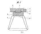
- FIG. 2 is a cross-sectional view of the millimeter wave antenna taken along line A-A ′ of FIG. 1.
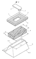
- FIG. 2 is an exploded view of the millimeter wave antenna of FIG. 1.
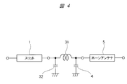
- FIG. 2 is an equivalent circuit diagram of the millimeter wave antenna of FIG. 1. It is sectional drawing which shows the millimeter wave antenna of the 2nd example in Embodiment 1 of this invention. It is sectional drawing which shows the millimeter wave antenna of the 3rd example in Embodiment 1 of this invention. It is sectional drawing which shows the millimeter wave antenna of the 4th example in Embodiment 1 of this invention.
- FIG. 10 is a cross-sectional view of the millimeter wave antenna taken along line A-A ′ of FIG. 9. It is a perspective view which shows the millimeter wave antenna of the 2nd example in Embodiment 2 of this invention. It is a perspective view which shows the millimeter wave antenna of the 1st example in Embodiment 3 of this invention.
- FIG. 13 is an exploded view of the millimeter wave antenna of FIG. 12. It is sectional drawing which shows the millimeter wave antenna of the 2nd example in Embodiment 3 of this invention.
- FIG. 22 is an equivalent circuit diagram of the millimeter wave antenna of FIG. 21.
- the constituent elements are not necessarily indispensable unless otherwise specified and apparently indispensable in principle. Needless to say.
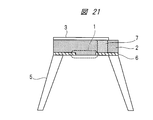
- FIG. 21 is a cross-sectional view showing a millimeter wave antenna in the comparison technique with respect to the present embodiment.
- 1 is a slit
- 2 is a circuit board
- 3 is a microstrip line
- 5 is a horn antenna
- 6 is a GND (ground) conductor
- 7 is an interlayer via that connects the interlayer conductors.
- the millimeter wave antenna shown in FIG. 21 is a millimeter wave antenna in which the slit 1 and the horn antenna 5 are directly overlapped, and a parasitic component is generated due to the difference in the shape of the metal conductor.
- a ridged horn antenna in the millimeter wave band it is necessary to reduce the parasitic component caused by the difference in the metal conductor of the transmission line conversion section.
- the wavelength in free space in the 76 GHz band is about 4 mm.
- the difference between the metal conductors In order to suppress the phase difference generated in the parasitic component to 10 degrees or less, the difference between the metal conductors must be 0.1 mm or less, which is 1/36 or less of the wavelength, and is almost equal to the minimum dimension at the time of metal mass production processing. Requires unrealistic costs.
- the slit provided in the circuit board filled with the dielectric having the dielectric constant er is 1 / ⁇ er of wavelength compression, the size of the hole provided in the metal conductor is reduced.
- the difference in conductor shape is enlarged and the parasitic component is increased. Therefore, since the structure of the connecting portion needs to be further reduced in size, the millimeter wave antenna in which the slit and the horn antenna are directly connected cannot realize a matching method commensurate with the mass production cost.
- a device is devised for the problems existing in the above-described comparative technique.
- the technical idea of the present embodiment in which this device has been devised is to increase the bandwidth of the transmission line by not using a frequency-dependent line in the propagation path.
- the present invention provides an antenna and a sensor using the same, which do not use a ⁇ / 2-size resonant antenna or a ⁇ / 4 matching device that limits the bandwidth.
- a slot made of a dielectric is provided between a slit as a radiating element and a horn antenna.
- the slot is a rectangular prism slot shape, and the cross-sectional shape is rectangular (rectangular), but the aspect ratio of this rectangle is longer than the slit in the long side direction (magnetic field direction) in order to increase the capacity.
- the slot is a slot shape of a concave column (concave column shape), and the cross-sectional shape is a concave shape.
- the aspect ratio of the concave shape is the length in the long side direction (magnetic field direction) in order to increase the capacity. Is formed sufficiently longer than the slit.
- filling the inside of the slot with a dielectric having a large dielectric constant also has the effect of increasing the capacitance value.
- the long side of the slot is formed longer than the long side of the opening of the horn antenna, a capacitive effect can be generated between the conductor surface forming the slit and the metal conductor surface of the horn antenna. It is.
- the length of the slot in the propagation direction is set to be less than 1 ⁇ 4 of the upper limit of the usable frequency band that causes lumped constant behavior in order to effectively function as a capacitive element.
- an impedance matching device to be a ⁇ -type LC circuit shown in FIG. 4 to be described later is formed by a conductor surface forming a slit, a slot made of a dielectric, and components of a metal conductor of a horn antenna.
- FIG. 1 is a perspective view showing a millimeter wave antenna of a first example in the first embodiment.
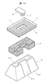
- FIG. 2 is a cross-sectional view of the millimeter wave antenna taken along line AA ′ of FIG. 3 is an exploded view of the millimeter wave antenna of FIG. 1 to 3, 1 is a slit, 2 is a circuit board, 3 is a microstrip line, 4 is a slot, 5 is a horn antenna, 6 is a GND (ground) conductor, and 7 is an interlayer via that connects interlayer conductors. It is.
- the electric field direction, magnetic field direction, and propagation direction are as shown in FIG.
- the electric field direction is the direction from the upper left to the lower right in FIG. 1
- the magnetic field direction is the direction orthogonal to the electric field direction (the direction from the upper right to the lower left in FIG. 1)
- the propagation direction is the direction orthogonal to the electric field direction and the magnetic field direction (FIG. 1). In the direction from top to bottom).
- the microstrip line 3 is formed on the upper surface of the circuit board 2
- the GND conductor 6 is formed on the lower surface of the circuit board 2
- the GND conductor 6 functions as a GND electrode of the microstrip line 3.
- the circuit board 2 is a multilayer board in which the metal conductors of the microstrip line 3 and the GND conductor 6 and a dielectric formed between the metal conductors are multilayered.
- the end of the microstrip line 3 is connected to the GND conductor 6 through the interlayer via 7 across the slit 1.
- the slit 1 is a rectangular hole provided in the GND conductor 6. This rectangular hole has a rectangular shape, the magnetic field direction is the long side, and the electric field direction is the short side.
- the electromagnetic wave between the microstrip line 3 and the GND conductor 6 propagates in the TEM mode, but is radiated as a TE01 mode radio wave when applied between the long sides of the slit 1.
- the lower frequency limit is f1
- the upper frequency limit is f2.
- the long side of the punched hole is set to have a length ⁇ 1 / (2 ⁇ e1) or more which is wavelength-compressed by the dielectric constant e1 of the circuit board 2 so that the cut-off frequency of the slit 1 is f1 or less.
- the horn antenna 5 radiates the TE01 mode radio wave radiated from the slit 1 to the space.
- the horn antenna 5 has a radiation opening 5-2 having an opening area of a desired rectangular shape (rectangular, magnetic field direction long side, electric field direction short side) for defining antenna gain and radiation direction, and a conductor surface.
- the signal input part of the horn antenna 5 adjacent to the slit 1 is a waveguide shape having an opening 5-1 having a rectangular shape (rectangular, magnetic field direction is long side, electric field direction is short side), and the long side is Since the antenna radiates into the space, the length is equal to or longer than the in-tube wavelength ⁇ 1 / 2 determined by the wavelength compression ⁇ 1 (dielectric constant 1).
- the length of the rectangular long sides of the slit 1 and the horn antenna 5 provided on the circuit board 2 has a relative ratio of ⁇ e1 times due to the intervening dielectric.
- the dielectric used for the circuit board 2 is a glass epoxy resin having a dielectric constant of 4
- the relative ratio of the lengths of the conductor long sides is as large as about twice.
- the millimeter wave antenna in which the slit 1 and the horn antenna 5 of the comparative technique shown in FIG. 21 described above when the slit 1 and the horn antenna 5 having different long side sizes are in contact, they are viewed from the slit 1 side.
- the horn antenna 5 is low impedance, and the slit 1 viewed from the horn antenna 5 side is treated as a high impedance transmission line, and the conductor discontinuity surface is an equivalent circuit shown in FIG.
- FIG. 22 is an equivalent circuit diagram of the millimeter wave antenna of FIG.
- a parasitic inductance 31 and a parasitic capacitance 32 are generated between the slit 1 and the horn antenna 5, and the parasitic inductance 31 is generated between the slit 1 and the horn antenna 5, and the parasitic capacitance 32 is on the slit 1 side. Between the ground potential and the GND potential.
- FIG. 4 is an equivalent circuit diagram of the millimeter wave antenna shown in FIGS. As shown in the equivalent circuit of FIG. 4, a ⁇ -type equivalent circuit is formed by the parasitic inductance 31, the parasitic capacitance 32, and the capacitive component of the slot 4.
- the length of the propagation direction of the slot 4 is 90 ° (with respect to the wavelength ⁇ 2 of the frequency upper limit f2 of the millimeter wave antenna) so that the equivalent circuit shown in FIG. 4 can be treated as a lumped constant circuit. It is desirable to be less than. That is, the length L3 in the propagation direction of the slot 4 shown in FIG. 3 is less than 1 ⁇ 4 of the wavelength ⁇ 2 of the use frequency upper limit f2. Also, the slot 4 shown in FIGS. 1 to 3 can increase the capacitance component by providing it larger than the conductor inner surface of the signal input portion of the horn antenna 5. In particular, it is possible to increase the capacitance component more effectively by increasing the size of the magnetic field direction in the slot 4.
- the length L1 of the slot 4 shown in FIG. 3 in the magnetic field direction is longer than the length L11 of the opening 5-1 of the horn antenna 5 in the magnetic field direction.
- the length L2 of the slot 4 in the electric field direction is also longer than the length L12 of the opening 5-1 of the horn antenna 5 in the electric field direction.
- the length of the slot 4 in the electric field direction is preferably equal to or shorter than the length of the short side of the slit 1 in order to increase the capacitance component.
- the capacitance component can be increased by a factor of e2.
- the capacitance component value in the slot 4 is a correction coefficient for the parasitic element, and is a design matter for optimizing the cross-sectional rectangular size, length (propagation direction), and dielectric constant e2 in the slot shape (square column) of the slot 4. .
- the slit 1 and the signal input portion of the horn antenna 5 are connected via a slot 4 filled with a dielectric having a dielectric constant e2 in a transmission line designed with a specific characteristic impedance, the discontinuous portion of the cross-sectional conductor Thus, it is possible to reduce the characteristic impedance difference and suppress the voltage standing wave ratio between the transmission lines. Therefore, by using the slot 4 as an impedance matching unit between the slit 1 and the horn antenna 5, it is possible to use a wide band in a millimeter wave antenna including the circuit board 2 in a wide band.
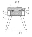
- FIG. 5 is a cross-sectional view showing a millimeter wave antenna of a second example in the first embodiment.
- 1 is a slit
- 2 is a circuit board
- 3 is a microstrip line
- 4 is a slot
- 5 is a horn antenna
- 6 is a GND conductor
- 7 is an interlayer via for connecting interlayer conductors
- 8 is a housing.
- the millimeter wave antenna shown in FIG. 5 is provided with a slot-shaped hole in the housing 8 to form a slot 4 filled with a dielectric having a dielectric constant e2.
- Various circuit components such as semiconductor components, passive components, and connectors are mounted on the circuit board 2 in order to realize a desired circuit operation.
- the substrate temperature changes due to heat generation in the circuit board 2 or the operating environment, a part or the whole of the circuit board 2 expands and warps.
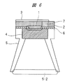
- FIG. 6 is a cross-sectional view showing a third example of a millimeter wave antenna according to the first embodiment.
- 1 is a slit
- 2 is a circuit board
- 3 is a microstrip line
- 4 is a slot
- 5 is a horn antenna
- 6 is a GND conductor
- 7 is an interlayer via that connects interlayer conductors.
- the housing 8 shown in FIG. 5 is integrated with the horn antenna 5, and a slot-shaped hole is provided in the signal input portion of the horn antenna 5 to fill it with a dielectric having a dielectric constant e2.
- a slot 4 is formed.
- FIG. 7 is a cross-sectional view showing a millimeter wave antenna of a fourth example in the first embodiment.
- 1 is a slit
- 2 is a circuit board
- 3 is a microstrip line
- 4 is a slot
- 5 is a horn antenna
- 6-1 and 6-2 are GND conductors
- 7 is an interlayer via for connecting interlayer conductors. It is.
- differences from the above-described example will be mainly described.
- the circuit board 2 is a multilayer board in which a dielectric layer having a dielectric constant e1 (on the microstrip line 3 side) and a dielectric layer having a dielectric constant e2 (on the horn antenna 5 side) are stacked.
- the dielectric layer having a dielectric constant e2 has a structure simulating a slot 4 in which interlayer vias 7 are arrayed in a square shape.
- FIG. 8 is a perspective view showing the slot 4 formed using the interlayer via 7 in the dielectric layer having the dielectric constant e2 of the circuit board 2.
- the GND conductor 6 includes a GND conductor 6-1 that forms the slit 1 and a GND conductor 6-2 that is in contact with the signal input portion of the horn antenna 5, and shares the potentials of the GND conductors 6-1 and 6-2. They are connected by interlayer vias 7.
- the inter-layer vias 7 (hereinafter referred to as via array 9) arrayed in a square shape are arranged outside the punched holes of the slit 1 so that the dielectric layer having the dielectric constant e2 inside the via array 9 is the above-described FIG.
- the thickness of the dielectric layer having the dielectric constant e2 is the length of the slot 4 (propagation direction), and the via inner surface distance of the via array 9 is equivalent to the rectangular cross-sectional size of the slot 4, and the layer thickness of the dielectric layer having the dielectric constant e2
- the vertical and horizontal size of the inner surface distance of the via array 9 is a design item of the capacitance component value shown in the above-described equivalent circuit of FIG.
- the capacitance value of the opening size of the slit 1 provided in the GND conductor 6-1 and the opening size of the signal input portion of the horn antenna 5 also vary depending on the relative difference from the via array 9, the opening size of the slit 1 and the like are set. It can also be used as an optimization design item.
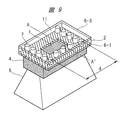
- FIG. 9 is a perspective view showing a millimeter wave antenna of the first example in the second embodiment.
- FIG. 10 is a cross-sectional view of the millimeter wave antenna taken along line AA ′ of FIG. 9 and 10, 1 is a slit, 2 is a circuit board, 11 is a pseudo waveguide line, 4 is a slot, 5 is a horn antenna, 6-1 and 6-3 are GND conductors, and 7 is an interlayer conductor. Is an interlayer via that connects the two.
- differences from the above-described example will be mainly described.
- the pseudo waveguide line 11 is formed on the circuit board 2 and is formed on the upper and lower conductor surfaces of the circuit board 2 connected by the interlayer vias 7-3.
- 6-1 a waveguide line in which a cutoff frequency is defined by a distance d between interlayer vias 7 arranged in the direction of the magnetic field in the propagation direction.
- the slit 1 is a rectangular hole provided in the GND conductor 6-1 on the lower surface side of the circuit board 2.
- the long side of the hole of the slit 1 and the distance between vias of the pseudo waveguide line 11 are lengths ⁇ 1 / (2 ⁇ e1) that are wavelength-compressed by the dielectric constant e1 of the circuit board 2 so that the cutoff frequency is f1 or less. ) Or more.
- the horn antenna 5 has a radiation opening 5-2 having a desired rectangular opening area for defining an antenna gain and a radiation direction, and has a tapered shape by a waveguide constituted by a conductor surface.
- the signal input portion of the horn antenna 5 adjacent to the slit 1 has a waveguide shape having a rectangular opening 5-1 and its long side is an antenna that radiates into space.
- the in-tube wavelength ⁇ 1 / 2 or more obtained by the dielectric constant 1) is obtained.
- the line is defined by a dielectric having a dielectric constant e1, and therefore the short side of the slit 1 and the dielectric constant e1
- the thickness of the dielectric is inevitably an approximate length.
- the length of the long side of the rectangular shape of the slit 1 and the horn antenna 5 provided on the circuit board 2 depends on the intervening dielectric. A relative ratio of ⁇ e1 occurs. Therefore, the conductor discontinuous surface becomes an equivalent circuit as shown in FIG.
- the slot 4 is disposed between the slit 1 and the horn antenna 5.
- a ⁇ -type equivalent circuit is formed by the parasitic inductance 31, the parasitic capacitance 32, and the capacitance component of the slot 4 as shown in the equivalent circuit of FIG.
- the capacitance component due to the slot 4 cancels out the high impedance component due to the parasitic inductance, and the impedance of the equivalent circuit is brought close to the line characteristic impedance of the slit 1 and the horn antenna 5, thereby suppressing the voltage standing wave ratio between the lines.
- the length in the propagation direction of the slot 4 is preferably such that the propagation phase rotation amount of the slot 4 is less than 90 ° so that the equivalent circuit shown in FIG. 4 described above can be handled as a lumped constant circuit.
- the slot 4 shown in FIG. 9 and FIG. 10 can increase the capacitance component by providing it larger than the conductor inner surface of the signal input portion of the horn antenna 5. In particular, it is possible to increase the capacitance component more effectively by increasing the size of the magnetic field direction in the slot 4. Further, the length of the slot 4 in the electric field direction is preferably equal to or shorter than the length of the short side of the slit 1 in order to increase the capacitance component.
- the capacitance component can be increased by a factor of e2.
- the capacitance component value in the slot 4 is a correction coefficient for the parasitic element, and is a design matter for optimizing the cross-sectional rectangular size, length (propagation direction), and dielectric constant e2 in the slot shape (square column) of the slot 4. .
- the discontinuous portion of the cross-sectional conductor can use a wide band.
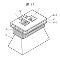
- FIG. 11 is a perspective view showing a millimeter wave antenna of a second example in the second embodiment.
- 1 is a slit
- 2 is a circuit board
- 12 is a coplanar line with a ground
- 4 is a slot
- 5 is a horn antenna
- 6-1 and 6-3 are GND conductors
- 7 is an interlayer connecting interlayer conductors. Beer.
- differences from the above-described example will be mainly described.
- the grounded coplanar line 12 is formed on the upper surface of the circuit board 2, the GND conductor 6-1 is formed on the lower surface of the circuit board 2, and the GND conductor 6-1 is connected to the grounded coplanar line. It functions as 12 GND electrodes.
- the end of the grounded coplanar line 12 is connected to the GND conductor 6-1 on the lower surface of the circuit board 2 and the GND conductor 6-3 on the upper surface of the circuit board 2 connected by the interlayer via 7.
- the slit 1 is a rectangular hole provided in the GND conductor 6-1.
- the electromagnetic wave between the coplanar line with ground 12 and the GND conductor 6-1 propagates mainly in the TEM mode, but is radiated as an electromagnetic wave in the TE01 mode by being applied between the long sides of the slit 1.
- the long side of the punched hole is a length ⁇ 1 / (2 ⁇ which is wavelength-compressed by the dielectric constant e1 of the circuit board 2 so that the cutoff frequency of the slit 1 is f1 or less.
- the slot 4 is disposed between the slit 1 and the horn antenna 5.
- a ⁇ -type equivalent circuit is formed by the parasitic inductance 31, the parasitic capacitance 32, and the capacitance component of the slot 4 as shown in the equivalent circuit of FIG.
- the discontinuous portion of the cross-sectional conductor can use a wide band.
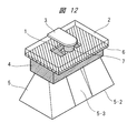
- FIG. 12 is a perspective view showing a millimeter wave antenna of the first example in the third embodiment.
- FIG. 13 is an exploded view of the millimeter wave antenna of FIG. 12 and 13, 1 is a slit, 2 is a circuit board, 3 is a microstrip line, 4 is a slot, 5 is a horn antenna, 6 is a GND conductor, and 7 is an interlayer via that connects interlayer conductors.
- differences from the above-described example will be mainly described.
- the microstrip line 3 is formed on the upper surface of the circuit board 2
- the GND conductor 6 is formed on the lower surface of the circuit board 2
- the GND conductor 6 is the GND of the microstrip line 3. Functions as an electrode.
- the end of the microstrip line 3 is connected to the GND conductor 6 through the interlayer via 7 across the slit 1.
- the slit 1 is a concave hole provided in the GND conductor 6.
- the electromagnetic wave between the microstrip line 3 and the GND conductor 6 propagates in the TEM mode, but is radiated as a TE01 mode radio wave when applied between the long sides of the slit 1.
- the lower frequency limit is f1
- the upper frequency limit is f2.
- the long side of the punched hole is set to have a length ⁇ 1 / (2 ⁇ e1) or more which is wavelength-compressed by the dielectric constant e1 of the circuit board 2 so that the cut-off frequency of the slit 1 is f1 or less.
- the characteristic impedance of the microstrip line 3 provided on the circuit board 2 is 50 ⁇ , the characteristic impedance is effectively maintained while maintaining the cut-off frequency of the slit 1 by making the shape of the hole of the slit 1 concave. Can be reduced.
- the horn antenna 5 has a radiation opening 5-2 having a desired concave opening area for defining an antenna gain and a radiation direction, and has a tapered shape by a waveguide constituted by a conductor surface.
- the signal input portion of the horn antenna 5 adjacent to the slit 1 has a waveguide shape having a concave opening 5-1, and its long side is an antenna that radiates into space. The length is equal to or longer than the guide wavelength ⁇ 1 / 2 determined by the ratio 1).
- Consistency with the spatial impedance of the atmosphere is achieved by converting impedance in the horn antenna 5 by gradually shortening the ridge-shaped protrusions toward the inner surface of the waveguide in the tapered waveguide.
- the horn antenna 5 needs a finite opening area that can obtain a desired radiation directivity, and the length of the horn antenna 5 itself is as long as 5 times the wavelength ⁇ 1 or more, so even if a ridge-shaped protrusion is provided. The length of the horn antenna 5 is not extended.
- the length of the concave long side of the slit 1 provided on the circuit board 2 and the horn antenna 5 has a relative ratio of ⁇ e1 times due to the intervening dielectric. Therefore, when the slit 1 and the horn antenna 5 having different long side sizes are in contact with each other, the horn antenna 5 viewed from the slit 1 side is a low impedance transmission line, and the slit 1 viewed from the horn antenna 5 side is a high impedance transmission line.
- the conductor discontinuity surface becomes an equivalent circuit as shown in FIG.
- a parasitic inductance 31 and a parasitic capacitance 32 are generated between the slit 1 and the horn antenna 5, and the parasitic inductance 31 is generated between the slit 1 and the horn antenna 5, and the parasitic capacitance 32 has a GND potential on the slit 1 side. Occurs during
- the slot 4 is a slot shape of a concave column (concave column shape), and the cross-sectional shape is a concave shape.
- Capacitance component due to slot 4 cancels high impedance component due to parasitic inductance, and impedance of equivalent circuit is made close to the line characteristic impedance of concave slit 1 and ridged horn antenna 5, thereby suppressing the voltage standing wave ratio between lines To do.
- the length of the propagation direction of the slot 4 is 90 ° (with respect to the wavelength ⁇ 2 of the frequency upper limit f2 of the millimeter wave antenna) so that the equivalent circuit shown in FIG. 4 can be treated as a lumped constant circuit. It is desirable to be less than
- the size of the slot 4 shown in FIG. 12 and FIG. 13 can be increased by providing a larger size than the inner surface of the conductor of the signal input portion of the horn antenna 5. In particular, it is possible to increase the capacitance component more effectively by increasing the size of the magnetic field direction in the slot 4.
- the length of the slot 4 in the electric field direction is preferably equal to or shorter than the length of the short side of the slit 1 in order to increase the capacitance component.
- the slot 4 when the slot 4 is filled with a dielectric having a dielectric constant e2, a capacitance component that establishes the above-described equivalent circuit of FIG. 4 can be realized by the effect of increasing the capacitance of the dielectric constant e2, and the slot 1 is longer than the length of the concave protrusion of the slit 1. It is possible to shorten the four concave projections.
- the capacitance component value in the slot 4 is a correction coefficient for the parasitic element, and is a design item for optimizing the concave section size of the slot 4, the length in the radio wave propagation direction, the length and width of the concave protrusion, and the dielectric constant e2. It is.
- the cross-sectional conductor is not affected. It is possible to reduce the characteristic impedance difference including the continuous part and to suppress the voltage standing wave ratio between the transmission lines, and it is possible to use the wide band in the millimeter wave antenna including the circuit board 2.
- FIG. 14 is a cross-sectional view showing a second example of the millimeter wave antenna according to the third embodiment.
- 1 is a slit
- 2 is a circuit board
- 3 is a microstrip line
- 4 is a slot
- 5 is a horn antenna
- 6-1 and 6-2 are GND conductors
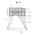
- 7 is an interlayer via that connects interlayer conductors. It is.
- differences from the above-described example will be mainly described.
- the circuit board 2 is a multilayer substrate in which a dielectric layer having a dielectric constant e1 and a dielectric layer having a dielectric constant e2 are stacked. It has a structure simulating a slot 4 in which 7 are arrayed in a square shape.
- the conductors of the slit 1, the slot 4 and the signal input portion of the horn antenna 5 have a concave shape.
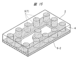
- FIG. 15 is a perspective view showing the slot 4 having a concave hole formed in the dielectric layer having the dielectric constant e2 of the circuit board 2 using the interlayer via 7.
- the GND conductor 6 includes a GND conductor 6-1 that forms the slit 1 and a GND conductor 6-2 that is in contact with the signal input portion of the horn antenna 5, and shares the potentials of the GND conductors 6-1 and 6-2. They are connected by interlayer vias 7.
- the interlayer vias 7 (via array 9) arrayed in a concave shape are arranged outside the punched holes of the slit 1, so that the dielectric layer having the dielectric constant e2 inside the via array 9 is the slot shown in FIG. 4 is realized.
- the thickness of the dielectric layer having the dielectric constant e2 is the length of the slot 4, the via inner surface distance of the via array 9 is equivalent to the concave size of the slot 4, the layer thickness of the dielectric layer having the dielectric constant e2, and the via array 9
- the vertical / horizontal size of the inner surface distance is a design item of the capacitance component value shown in the equivalent circuit of FIG. 4 described above.
- the capacitance value of the opening size of the slit 1 provided in the GND conductor 6-1 and the opening size of the signal input portion of the horn antenna 5 also vary depending on the relative difference from the via array 9, the opening size of the slit 1 and the like are set. It can also be used as an optimization design item.
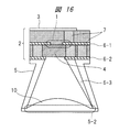
- FIG. 16 is a cross-sectional view showing a millimeter wave antenna of the first example in the fourth embodiment.
- 1 is a slit
- 2 is a circuit board
- 3 is a microstrip line
- 4 is a slot
- 5 is a horn antenna
- 6-1 and 6-2 are GND conductors
- 7 is an interlayer via that connects interlayer conductors.
- Reference numeral 10 denotes a dielectric lens.
- the millimeter wave antenna shown in FIG. 16 is an example in which a dielectric lens 10 is added to the millimeter wave antenna shown in FIGS. 14 and 15 described above.
- the present embodiment is not limited to this, and can also be applied to the other millimeter wave antennas shown in FIGS. 1 to 13 described above.
- the circuit board 2 is a multilayer substrate in which a dielectric layer having a dielectric constant e1 and a dielectric layer having a dielectric constant e2 are stacked. It has a structure simulating a slot 4 in which 7 are arrayed in a square shape.
- the conductors of the slit 1, the slot 4 and the signal input portion of the horn antenna 5 have a concave shape.
- the slot 4 is constituted by the GND conductors 6-1 and 6-2 and the interlayer via 7 in the circuit board 2 as shown in FIGS. 14 and 15 described above.
- the dielectric lens 10 is a lens that is installed in the radiation opening 5-2 of the horn antenna 5 and adjusts the phase of the electromagnetic wave diffused radially in the horn antenna 5 in the propagation direction.
- a single-sided convex lens, a double-sided convex lens, or a single-sided cylindrical lens is used.
- a one-side convex lens that is convex on the signal input part side of the horn antenna 5 is used.
- the lens curvature and the lens focal length can be adjusted by increasing the dielectric constant of the lens material, and the length of the horn antenna 5 can be shortened by using a lens material having a high dielectric constant.
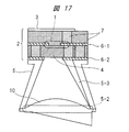
- FIG. 17 is a cross-sectional view showing a second example of the millimeter wave antenna according to the fourth embodiment.
- the millimeter wave antenna shown in FIG. 17 is an example in which the dielectric lens 10 of the millimeter wave antenna shown in FIG. 16 is changed. In this example, differences from the above-described example will be mainly described.
- the lens 10 is installed in the radiation opening 5-2 of the horn antenna 5.
- the dielectric lens 10 as shown in FIG. 17 is provided, the propagation direction of electromagnetic waves (radiation direction) can be deflected by the lens refractive index.
- the millimeter wave sensor according to the fifth embodiment will be described with reference to FIGS.
- the millimeter wave sensor according to the fifth embodiment is a sensor using the millimeter wave antenna described in the first to fourth embodiments.
- FIG. 18 is a perspective view showing a millimeter wave sensor of the first example in the fifth embodiment.
- 2 is a circuit board
- 3 is a microstrip line
- 5 is a horn antenna
- 21 is a millimeter wave band RF (Radio Frequency) circuit
- 22 is an ADC (Analog / Digital Converter) / DAC (Digital / Analog Converter)
- Reference numeral 23 denotes a DSP (Digital Signal Processing Unit)
- 24 denotes a power supply unit
- 26 denotes an input / output terminal.
- the circuit board 2, the microstrip line 3, and the horn antenna 5 are components of the millimeter wave antenna shown in the first to fourth embodiments.
- the millimeter wave sensor shown in FIG. 18 is an example using the millimeter wave antenna shown in FIGS. 12 and 13 described above.
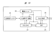
- FIG. 19 is a circuit configuration diagram of the millimeter wave sensor of FIG.
- reference numeral 25 denotes a transmitting / receiving antenna, which corresponds to the millimeter wave antenna described in the first to fourth embodiments.
- the millimeter wave signal generated by the millimeter wave band RF circuit 21 is radiated from the horn antenna 5 via the microstrip line 3 of the transmission / reception antenna 25, and It reaches the object to be measured and is reflected, and is received by the horn antenna 5 again.
- the received millimeter wave signal includes a Doppler signal due to a relative speed difference, and the millimeter wave band RF circuit 21 extracts the Doppler signal by comparing the received wave with the transmitted wave.
- the extracted Doppler signal is converted into a digital signal by the ADC of the ADC / DAC 22, and Fourier-transformed by the DSP 23 to detect and analyze the Doppler frequency, thereby calculating the relative operation state of the object to be measured such as a relative speed. .
- the processing result by the DSP 23 can be output through the input / output terminal 26. Further, a digital signal input through the input / output terminal 26 can be processed by the DSP 23, converted into an analog signal by the DAC of the ADC / DAC 22, and transmitted to the millimeter wave band RF circuit 21.
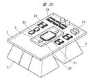
- FIG. 20 is a perspective view showing a millimeter wave sensor of a second example in the fifth embodiment.
- 2 is a circuit board
- 3 is a microstrip line
- 5 is a horn antenna
- 21 is a millimeter wave band RF circuit
- 22 is an ADC / DAC
- 23 is a DSP
- 24 is a power supply unit
- 26 is an input / output terminal
- 28 Is a cover that covers the millimeter-wave band RF circuit 21.
- a plurality of horn antennas 5 are used for the purpose of reducing isolation between transmission and reception and improving the dynamic lens of the receiving circuit (FIG. 20 shows two examples). Separate the antenna. Further, if two or more horn antennas 5 are used for transmission and reception, respectively, a phase difference between a plurality of antennas is actively provided by the millimeter wave band RF circuit 21, thereby scanning in the radial direction (active beam scanning). ) Is feasible. Furthermore, if a plurality of horn antennas 5 for both transmission and reception are provided and a dielectric lens that changes the radiation direction shown in FIG. 17 to an arbitrary direction is used, a plurality of antenna beams having different radiation directions can be realized. is there.
- millimeter wave band RF circuit 21, ADC / DAC 22 and DSP 23 are mounted on the same substrate surface to reduce mounting costs. Since the millimeter wave signal has a short wavelength, leakage of the millimeter wave signal from the millimeter wave band RF circuit 21 or the microstrip line 3 to the ADC / DAC 22 or DSP 23 occurs, resulting in sensing malfunction.
- a lid 28 is provided to cover the millimeter wave band RF circuit 21 and the microstrip line 3.
- the millimeter wave band RF circuit 21 and the microstrip line 3 are formed on the upper surface of the circuit board 2, and are electrically connected by the horn antenna 5 and the GND conductor 6 in the circuit board 2. Isolated. If the millimeter wave antenna structure in the present embodiment described above is used, it is possible to shield the millimeter wave signal inside the millimeter wave sensor in the closed space formed by the circuit board 2 and the lid 28.
- the lid 28 is made of a metal having a shielding effect or a conductive resin such as carbon.
- a material such as carbon that uses dielectric loss due to molecular polarization reaction or ferrite that uses magnetic loss is used as part of the resin composition, and a lid 28 that achieves both radio wave absorption characteristics and radio wave shielding effects is used. For example, low-cost productivity of injection molding and light weight of the resin material can be realized.
- the transmission line can be widened by not using the frequency-dependent line in the propagation path.
- Capacitance can be increased by providing a dielectric slot 4 between the slit 1 and the horn antenna 5.
- the capacitance value can be increased by filling the slot 4 with a dielectric having a high dielectric constant.
- the slot 4 By making the length of the propagation direction of the slot 4 less than 1 ⁇ 4 of the wavelength of the upper limit of the use frequency, the slot 4 can effectively function as a capacitive element and behave as a lumped constant. it can.
- (4) By forming the long side of the rectangular or concave shape of the slot 4 longer than the long side of the opening of the horn antenna 5, the gap between the conductor surface forming the slit 1 and the metal conductor surface of the horn antenna 5 Can also produce capacitive effects.
Landscapes
- Engineering & Computer Science (AREA)
- Radar, Positioning & Navigation (AREA)
- Remote Sensing (AREA)
- Computer Networks & Wireless Communication (AREA)
- Physics & Mathematics (AREA)
- General Physics & Mathematics (AREA)
- Waveguide Aerials (AREA)
- Radar Systems Or Details Thereof (AREA)
- Aerials With Secondary Devices (AREA)
Abstract
伝搬経路中に周波数依存性のある線路を用いないことで伝送線路の広帯域化を図る技術である。ミリ波アンテナは、回路基板2の第1面に形成されたGND導体6に設けたスリット1と、第1開口部および第2開口部を設けたホーンアンテナ5と、スリット1とホーンアンテナ5の第1開口部との間に設けたスロット形状(スロット4)のインピーダンス整合器と、を有する。インピーダンス整合器は、回路基板2を構成する誘電体とは誘電率の異なる誘電体によって満たされたスロット形状である。インピーダンス整合器は、スロット形状の伝搬方向の長さが利用周波数上限の波長の1/4未満である。インピーダンス整合器は、スロット形状の矩形形状の磁界方向のサイズがホーンアンテナ5の第1開口部より大きい。
Description
本発明は、ミリ波帯電磁波を放射するミリ波アンテナおよびそれを用いたミリ波センサに関するものである。
大気の特性インピーダンスは、真空の誘電率ε0、透磁率μ0からおおよそ計算可能であり、377Ω程度である。これに対し、高周波回路に用いられる特性インピーダンスは、50Ω系を用いる。これらのインピーダンス比は6倍と大きく(電圧定在波比VSWR=7.5)、50Ω系の伝送線路から大気への放射はアンテナ長がλ/2となるダイポールアンテナに代表されるように共振系のアンテナシステムを用いる。ミリ波帯でよく採用されているパッチ素子も、導体サイズがλ/2長さとなる共振を利用したアンテナである。
パッチアンテナは、平面基板上の導体面に作製できるため、薄型化や低コスト化が容易である。ミリ波帯(76GHz)での利得20dBi以上となる開口面積は5cm程度の大きさを必要とし、この面積全面に配置したパッチ素子からミリ波電波を効率よく放射するように、トーナメント型や枝型(特許文献1)、シリーズフェッド型(特許文献2)などの様々な給電回路がある。この給電回路は、1つの給電点からインピーダンス整合を図りつつパッチ素子へ電力分配するため、λ/4整合器を多用しながら設計する。よって、パッチ素子とλ/4整合器を用いたパッチアレイアンテナでは、良好な反射特性が得られる周波数帯域(以下、利用帯域と略す)はキャリア周波数の5%程度である。
これに対し、導波管を用いたホーンアンテナは、カットオフ周波数よりも高い周波数でハイパス特性であるために広帯域である。しかし、導波管の特性インピーダンスは300Ωと高く、50Ω系伝送路と接続するには反射係数が大きい線路である。この対策として、パッチ素子による共振器を介したマイクロストリップ-導波管変換器(特許文献3)やλ/4整合器を複数利用したミリ波帯送受信機(特許文献4)が検討されている。これらの構造に用いられるパッチ素子やλ/4整合器は、多層基板の金属導体に設ける。このような変換構造においても広帯域化を図るには、共振周波数の異なるパッチ素子を複数用いる方法や、λ/4整合器を複数利用して特性インピーダンス変化量が小さくなるように段階的に配置する方法が採られており、必然的に多層基板の層数が多く加工コストが高い問題が生じている。
ホーンアンテナには、信号入力部にリッジ構造を設け、低インピーダンス化したアンテナが存在する。導波管構造にはカットオフ周波数があり、ハイパス特性の広帯域な電気特性を有する。一般に製造されているリッジ付ホーンアンテナは、伝送線路入力部が同軸構造である。同軸構造とリッジ構造の金属導体の差異から生じる寄生成分は存在するが、波長1cm以上であるマイクロ波帯では位相変動が小さく、50Ω系伝送路への影響は小さい。
前述した特許文献3に記載された技術では、マイクロストリップ線路などの伝送線路からホーンアンテナに接続する際、放射素子にスリットを用いる。スリットの開口形状は矩形であり、カットオフ周波数を有するハイパス特性の伝送線路であるため、広帯域化が期待される放射素子である。スリットの矩形開口部の長辺寸法は、誘電率により波長圧縮されて小型である。
一方、ホーンアンテナの矩形開口部の長辺サイズは、利用周波数より十分低いカットオフ周波数となるように、λ/2以上の長さを必要とする。広帯域化の目的で、ホーンアンテナの特性インピーダンスをスリット側に近づけると、ホーンアンテナの矩形開口部の縦横比は電界方向の長さが短くなるように(容量が増すように)形成される。従って、スリットとホーンアンテナの開口部を直接重ねた接続部では、スリット側から見たインピーダンスは容量性の増した線路(低インピーダンスな線路)と見え、逆にホーンアンテナ側から見れば誘導性の増した線路(開口部の長辺が短いために高インピーダンスな線路)と等価な回路である。
このように、スリットとホーンアンテナを直接重ねた接続部では、周波数特性の広帯域化を図るため、スリットとホーンアンテナとの特性インピーダンスを調整するが、互いの誘電体媒体が異なるために開口部のサイズに差異が生じ、金属導体の差異形状により、キャパシタンス成分とインダクタンス成分の寄生素子が発生する。この金属導体の差異形状による寄生素子を、周波数に依存せずに集中定数的に取り扱えるようにする必要がある。
本発明の目的は、伝搬経路中に周波数依存性のある線路を用いないことで伝送線路の広帯域化を図る技術を提供することにある。
本発明の前記ならびにその他の目的と新規な特徴は、本明細書の記述および添付図面から明らかになるであろう。
本願において開示される発明のうち、代表的なものの概要を簡単に説明すれば、次のとおりである。
一実施の形態におけるミリ波アンテナは、回路基板の第1面に形成された第1金属導体に設けたスリットと、第1開口部および第2開口部を設けたホーンアンテナと、スリットとホーンアンテナの第1開口部との間に設けたスロット形状のインピーダンス整合器と、を有する。
一実施の形態におけるミリ波センサは、回路基板上に、RF回路と、ADC/DAC、DSPおよび電源回路の少なくとも1つの電気回路とが設けられ、RF回路で生成された電気信号を、回路基板の金属導体に設けたスリットおよびインピーダンス整合器を介してホーンアンテナによって送受信し、電気回路にて、送受信信号の差分から検知したドップラー周波数より速度成分を算出するセンサとして機能するように構成されている。
本願において開示される発明のうち、代表的なものによって得られる効果を簡単に説明すれば以下の通りである。
一実施の形態によれば、伝搬経路中に周波数依存性のある線路を用いないことで伝送線路の広帯域化を図ることができる。
以下の実施の形態においては、便宜上その必要があるときは、複数のセクションまたは実施の形態に分割して説明するが、特に明示した場合を除き、それらは互いに無関係なものではなく、一方は他方の一部または全部の変形例、詳細、補足説明などの関係にある。
また、以下の実施の形態において、要素の数など(個数、数値、量、範囲などを含む)に言及する場合、特に明示した場合および原理的に明らかに特定の数に限定される場合などを除き、その特定の数に限定されるものではなく、特定の数以上でも以下でもよい。
さらに、以下の実施の形態において、その構成要素(要素ステップなども含む)は、特に明示した場合および原理的に明らかに必須であると考えられる場合などを除き、必ずしも必須のものではないことは言うまでもない。
同様に、以下の実施の形態において、構成要素などの形状、位置関係などに言及するときは、特に明示した場合および原理的に明らかにそうではないと考えられる場合などを除き、実質的にその形状などに近似または類似するものなどを含むものとする。このことは、上記数値および範囲についても同様である。
また、実施の形態を説明するための全図において、同一の部材には原則として同一の符号を付し、その繰り返しの説明は省略する。なお、図面を分かり易くするために、斜視図や分解図などであってもハッチングを付す場合があり、また断面図であってもハッチングを省略する場合があり、さらに各図において部分的にハッチングを付す場合あるいは省略する場合もある。
また、以下の実施の形態においては、本発明の特徴を分かり易くするために、本実施の形態に対する比較技術と比較して説明する。まず、本実施の形態に対する比較技術を説明する。
[本実施の形態に対する比較技術]
本実施の形態に対する比較技術におけるミリ波アンテナについて、図21を用いて説明する。図21は、本実施の形態に対する比較技術におけるミリ波アンテナを示す断面図である。
本実施の形態に対する比較技術におけるミリ波アンテナについて、図21を用いて説明する。図21は、本実施の形態に対する比較技術におけるミリ波アンテナを示す断面図である。
図21において、1はスリットであり、2は回路基板、3はマイクロストリップ線路、5はホーンアンテナ、6はGND(グランド)導体、7は層間導体を接続する層間ビアである。図21に示すミリ波アンテナは、スリット1とホーンアンテナ5とを直接重ねたミリ波アンテナであり、金属導体の形状の差により寄生成分が発生する。ミリ波帯でリッジ付ホーンアンテナを採用するには、伝送線路変換部の金属導体の差異で生じる寄生成分を小さくする必要がある。76GHz帯での自由空間での波長は約4mmである。寄生成分に生じる位相差を10度以下に抑えるには、金属導体の差異は波長の1/36以下となる0.1mm以下にする必要があり、金属量産加工時の最小寸法とほぼ等しく、量産には非現実的なコストが必要である。
さらに、誘電率erの誘電体で満たされた回路基板に設けたスリットは、1/√erの波長圧縮が生じるために、金属導体に設けた抜き穴のサイズが小型化する。これらの線路をリッジ付ホーンアンテナに接続すると、導体形状の差異が拡大して寄生成分が増大する。従って、接続部の構造はさらに小型化が必要なため、スリットとホーンアンテナとを直接接続したミリ波アンテナは、量産コストに見合う整合方法が実現できていない。
そこで、本実施の形態では、上述した比較技術に存在する課題に対する工夫を施している。この工夫を施した本実施の形態における技術的思想は、伝搬経路中に周波数依存性のある線路を用いないことで伝送線路の広帯域化を図ることである。言い換えれば、帯域制限となるλ/2サイズの共振系アンテナやλ/4整合器を用いずに、広帯域化するアンテナおよびそれを用いたセンサを提供するものである。
本実施の形態における技術的思想を実現するための手段として、放射素子であるスリットとホーンアンテナとの間に誘電体によるスロットを設ける。スロットは、四角柱のスロット形状であり、断面形状は矩形形状(長方形)であるが、この矩形の縦横比は容量性を増すために長辺方向(磁界方向)の長さをスリットより十分長く形成する。あるいは、スロットは、凹型柱(凹型形状の柱状)のスロット形状であり、断面形状は凹型形状であるが、この凹型の縦横比は容量性を増すために長辺方向(磁界方向)の長さをスリットより十分長く形成する。また、誘電率の大きな誘電体を用いてスロット内を満たすことでも容量値を増加させる効果がある。また、スロットの長辺をホーンアンテナの開口部の長辺よりも長く形成すれば、スリットを形成する導体面とホーンアンテナの金属導体面との間にも容量性の効果を生成することが可能である。また、スロットの伝搬方向の長さは、容量性の素子として効果的に機能させるために、集中定数的な振る舞いとなる利用周波数帯域上限の波長の1/4未満とする。
これらの手段による効果として、スリットを形成する導体面、誘電体によるスロット、およびホーンアンテナの金属導体の構成要素により、後述する図4に示すπ型のLC回路となるインピーダンス整合器を形成する。これにより、後述する図22に示す誘導性の高インピーダンスを打ち消す容量性成分が付加されることで、インピーダンス整合器の特性インピーダンスを判断指数である電圧定在波比VSWR=1に近づけられるように、スリットやホーンアンテナの値に寄せることが可能となる。従って、スリットやホーンアンテナの広帯域性を犠牲にすることなく、伝送線路間の反射特性を改善した低損失のミリ波帯のアンテナ、およびそれを用いたセンサを実現することができる。
以下では、上述した本実施の形態における技術的思想、これを実現するための手段、この手段による効果などについて、図面を参照しながら説明する。
[実施の形態1]
本実施の形態1におけるミリ波アンテナについて、図1~図8を用いて説明する。
本実施の形態1におけるミリ波アンテナについて、図1~図8を用いて説明する。
<実施の形態1における第1例>
図1は、本実施の形態1における第1例のミリ波アンテナを示す斜視図である。図2は、図1のA-A’線によるミリ波アンテナの断面図である。図3は、図1のミリ波アンテナの分解図である。図1~図3において、1はスリットであり、2は回路基板、3はマイクロストリップ線路、4はスロット、5はホーンアンテナ、6はGND(グランド)導体、7は層間導体を接続する層間ビアである。このミリ波アンテナにおいて、電界方向、磁界方向、伝搬方向は、図1に示した通りである。電界方向は図1において左上から右下への方向、磁界方向は電界方向に直交する方向(図1において右上から左下への方向)、伝搬方向は電界方向および磁界方向に直交する方向(図1において上から下への方向)である。
図1は、本実施の形態1における第1例のミリ波アンテナを示す斜視図である。図2は、図1のA-A’線によるミリ波アンテナの断面図である。図3は、図1のミリ波アンテナの分解図である。図1~図3において、1はスリットであり、2は回路基板、3はマイクロストリップ線路、4はスロット、5はホーンアンテナ、6はGND(グランド)導体、7は層間導体を接続する層間ビアである。このミリ波アンテナにおいて、電界方向、磁界方向、伝搬方向は、図1に示した通りである。電界方向は図1において左上から右下への方向、磁界方向は電界方向に直交する方向(図1において右上から左下への方向)、伝搬方向は電界方向および磁界方向に直交する方向(図1において上から下への方向)である。
このミリ波アンテナにおいて、マイクロストリップ線路3は回路基板2の上面に形成され、GND導体6は回路基板2の下面に形成され、GND導体6がマイクロストリップ線路3のGND電極として機能する。回路基板2は、マイクロストリップ線路3およびGND導体6の金属導体と、この金属導体間に形成された誘電体とを多層化した多層基板である。マイクロストリップ線路3の末端は、スリット1を跨いで層間ビア7を介してGND導体6と接続する。スリット1は、GND導体6に設けられた矩形状の抜き穴である。この矩形状の抜き穴は、長方形からなり、磁界方向が長辺であり、電界方向が短辺である。マイクロストリップ線路3とGND導体6との間の電磁波はTEMモードで伝搬するが、スリット1の長辺間に加えられることでTE01モードの電波として放射される。ミリ波アンテナを通過する電磁波の利用帯域において、周波数下限をf1、周波数上限をf2とする。スリット1のカットオフ周波数がf1以下となるように、抜き穴の長辺は回路基板2の誘電率e1により波長圧縮した長さλ1/(2√e1)以上とする。
ホーンアンテナ5は、スリット1から放射されたTE01モードの電波を空間に放射する。ホーンアンテナ5は、アンテナ利得や放射方向を定義するための所望の矩形状(長方形、磁界方向が長辺、電界方向が短辺)の開口面積による放射開口部5-2を有し、導体面により構成された導波管によるテーパ状の形状を有する。スリット1と近接するホーンアンテナ5の信号入力部は、矩形状(長方形、磁界方向が長辺、電界方向が短辺)の開口部5-1を有する導波管形状であり、その長辺は、空間に放射するアンテナであるため、波長圧縮√1(誘電率1)によって求まる管内波長λ1/2以上の長さとなる。
回路基板2に設けられるスリット1とホーンアンテナ5の矩形状の長辺の長さは、媒介する誘電体により√e1倍の相対比が生じる。回路基板2に用いる誘電体が誘電率4のガラスエポキシ樹脂である場合、導体長辺の長さの相対比は約2倍と大きい。上述した図21に示した比較技術のスリット1とホーンアンテナ5とを直接接続したミリ波アンテナにおいて、導体の長辺サイズが異なるスリット1とホーンアンテナ5とが接する場合、スリット1側から見たホーンアンテナ5は低インピーダンス的、ホーンアンテナ5側から見たスリット1は高インピーダンス的な伝送線路として扱われ、導体不連続面が図22に示す等価回路となる。
図22は、図21のミリ波アンテナの等価回路図である。図22において、スリット1とホーンアンテナ5との間に、寄生インダクタンス31と寄生キャパシタンス32とが生成され、寄生インダクタンス31はスリット1とホーンアンテナ5との間に生じ、寄生キャパシタンス32はスリット1側にGND電位との間に生ずる。
これに対して、図1~図3に示すミリ波アンテナでは、スロット4をスリット1とホーンアンテナ5との間に配置する。スロット4は、四角柱のスロット形状である。ミリ波アンテナにスロット4を追加することで、図4のような等価回路となる。図4は、図1~図3に示すミリ波アンテナの等価回路図である。図4の等価回路に示すように、寄生インダクタンス31と寄生キャパシタンス32とスロット4による容量成分とによりπ型の等価回路を形成する。スロット4による容量成分で寄生インダクタンスによる高インピーダンス成分を相殺し、等価回路のインピーダンスをスリット1およびホーンアンテナ5の線路特性インピーダンスに近づけることで、線路間の電圧定在波比を抑制する。すなわち、特性インピーダンスを、判断指数である電圧定在波比VSWR=1に近づける。
スロット4の伝搬方向の長さは、図4に示す等価回路が集中定数回路として扱えるように、スロット4の伝搬位相回転量は90°(ミリ波アンテナの周波数上限f2の波長λ2に対して)未満となることが望ましい。すなわち、図3に示すスロット4の伝搬方向の長さL3は、利用周波数上限f2の波長λ2の1/4未満である。また、図1~図3に示すスロット4は、ホーンアンテナ5の信号入力部の導体内面よりも大きく設けることで容量成分を増加させることが可能である。特に、スロット4内の磁界方向のサイズを広げることで容量成分をより効果的に増加させることが可能である。すなわち、図3に示すスロット4の磁界方向の長さL1は、ホーンアンテナ5の開口部5-1の磁界方向の長さL11よりも長い。また、図3に示すスロット4の例では、スロット4の電界方向の長さL2も、ホーンアンテナ5の開口部5-1の電界方向の長さL12よりも長くなっている。また、スロット4の電界方向の長さは、容量成分を増すためにスリット1の短辺の長さ以下とすることが望ましい。さらに、スロット4を誘電率e2の誘電体で満たすと、容量成分をe2倍に増加可能である。スロット4における容量成分値は、寄生素子に対する補正係数であり、スロット4のスロット形状(四角柱)における断面矩形サイズ、長さ(伝搬方向)、誘電率e2を最適化するための設計事項である。
上記スリット1および上記ホーンアンテナ5の信号入力部を特定の特性インピーダンスで設計された伝送路において、誘電率e2の誘電体で満たされたスロット4を介して接続すれば、断面導体の不連続部を含め、特性インピーダンス差を小さくし、伝送路間の電圧定在波比を抑えることが可能となる。従って、スロット4をスリット1とホーンアンテナ5との間のインピーダンス整合器として利用することで、回路基板2を含むミリ波アンテナで利用帯域を広帯域に用いることが可能である。
<実施の形態1における第2例>
図5は、本実施の形態1における第2例のミリ波アンテナを示す断面図である。図5において、1はスリットであり、2は回路基板、3はマイクロストリップ線路、4はスロット、5はホーンアンテナ、6はGND導体、7は層間導体を接続する層間ビア、8は筐体である。この例では、上述した例と異なる点を主に説明する。
図5は、本実施の形態1における第2例のミリ波アンテナを示す断面図である。図5において、1はスリットであり、2は回路基板、3はマイクロストリップ線路、4はスロット、5はホーンアンテナ、6はGND導体、7は層間導体を接続する層間ビア、8は筐体である。この例では、上述した例と異なる点を主に説明する。
図5に示すミリ波アンテナは、筐体8にスロット形状の抜き穴を設け、誘電率e2の誘電体で満たしたスロット4を形成する。上記回路基板2には、所望の回路動作を実現すべく半導体部品や受動部品、コネクタなどの様々な回路部品が搭載される。回路基板2での発熱や動作環境により基板温度が変化する場合、回路基板2の一部もしくは全体が膨張して反り返りが発生する。回路基板2およびホーンアンテナ5を筐体8に固定することにより、熱応力によるスロット4との位置ずれや分離を抑制し、機械的に安定したミリ波アンテナを形成することが可能である。
<実施の形態1における第3例>
図6は、本実施の形態1における第3例のミリ波アンテナを示す断面図である。図6において、1はスリットであり、2は回路基板、3はマイクロストリップ線路、4はスロット、5はホーンアンテナ、6はGND導体、7は層間導体を接続する層間ビアである。この例では、上述した例と異なる点を主に説明する。
図6は、本実施の形態1における第3例のミリ波アンテナを示す断面図である。図6において、1はスリットであり、2は回路基板、3はマイクロストリップ線路、4はスロット、5はホーンアンテナ、6はGND導体、7は層間導体を接続する層間ビアである。この例では、上述した例と異なる点を主に説明する。
図6に示すミリ波アンテナは、図5に示した筐体8をホーンアンテナ5と一体化し、ホーンアンテナ5の信号入力部にスロット形状の抜き穴を設け、誘電率e2の誘電体で満たしたスロット4を形成する。回路基板2をホーンアンテナ5に固定することにより、スロット4との位置ずれや分離を抑制し、機械的に安定したミリ波アンテナを形成することが可能である。
<実施の形態1における第4例>
図7は、本実施の形態1における第4例のミリ波アンテナを示す断面図である。図7において、1はスリットであり、2は回路基板、3はマイクロストリップ線路、4はスロット、5はホーンアンテナ、6-1,6-2はGND導体、7は層間導体を接続する層間ビアである。この例では、上述した例と異なる点を主に説明する。
図7は、本実施の形態1における第4例のミリ波アンテナを示す断面図である。図7において、1はスリットであり、2は回路基板、3はマイクロストリップ線路、4はスロット、5はホーンアンテナ、6-1,6-2はGND導体、7は層間導体を接続する層間ビアである。この例では、上述した例と異なる点を主に説明する。
図7に示すミリ波アンテナにおいて、回路基板2は、誘電率e1の誘電体層(マイクロストリップ線路3側)と誘電率e2の誘電体層(ホーンアンテナ5側)とを積層した複層基板であり、誘電率e2の誘電体層には層間ビア7を四角形状にアレイ化したスロット4を模擬した構造を有する。
図8は、回路基板2の誘電率e2の誘電体層に層間ビア7を用いて形成したスロット4を示す斜視図である。GND導体6は、スリット1を形成するGND導体6-1と、ホーンアンテナ5の信号入力部と接するGND導体6-2とからなり、GND導体6-1,6-2の電位を共通化する層間ビア7により接続されている。四角形状にアレイ化された層間ビア7(以下、ビアアレイ9と記す)は、スリット1の抜き穴より外側に配置することで、ビアアレイ9の内側の誘電率e2の誘電体層が上述した図1などに示すスロット4と同等の機能を実現する。誘電率e2の誘電体層の厚さはスロット4の長さ(伝搬方向)となり、ビアアレイ9のビア内面距離はスロット4の断面矩形サイズと等価であり、誘電率e2の誘電体層の層厚さ、ビアアレイ9の内面距離の縦横サイズが、上述した図4の等価回路に示す容量成分値の設計事項となる。また、GND導体6-1に設けたスリット1の開口サイズ、ホーンアンテナ5の信号入力部の開口サイズも、ビアアレイ9との相対的差分により容量値が変動するため、スリット1の開口サイズなどを最適化設計事項として利用することも可能である。
[実施の形態2]
本実施の形態2におけるミリ波アンテナについて、図9~図11を用いて説明する。
本実施の形態2におけるミリ波アンテナについて、図9~図11を用いて説明する。
<実施の形態2における第1例>
図9は、本実施の形態2における第1例のミリ波アンテナを示す斜視図である。図10は、図9のA-A’線によるミリ波アンテナの断面図である。図9および図10において、1はスリットであり、2は回路基板、11は擬似導波管線路、4はスロット、5はホーンアンテナ、6-1,6-3はGND導体、7は層間導体を接続する層間ビアである。この例では、上述した例と異なる点を主に説明する。
図9は、本実施の形態2における第1例のミリ波アンテナを示す斜視図である。図10は、図9のA-A’線によるミリ波アンテナの断面図である。図9および図10において、1はスリットであり、2は回路基板、11は擬似導波管線路、4はスロット、5はホーンアンテナ、6-1,6-3はGND導体、7は層間導体を接続する層間ビアである。この例では、上述した例と異なる点を主に説明する。
図9および図10に示すミリ波アンテナにおいて、擬似導波管線路11は、回路基板2に形成され、層間ビア7で接続された回路基板2の上下導体面に形成されたGND導体6-3,6-1間を伝搬する電磁波に対し、伝搬方向の磁界方向に配した層間ビア7間の距離dによりカットオフ周波数を定義した導波管線路である。スリット1は、回路基板2の下面側のGND導体6-1に設けられた矩形状の抜き穴である。スリット1の抜き穴の長辺、および擬似導波管線路11のビア間距離はカットオフ周波数がf1以下となるように回路基板2の誘電率e1により波長圧縮した長さλ1/(2√e1)以上とする。
ホーンアンテナ5は、アンテナ利得や放射方向を定義するための所望の矩形状の開口面積による放射開口部5-2を有し、導体面により構成された導波管によるテーパ状の形状を有する。スリット1と近接するホーンアンテナ5の信号入力部は、矩形状の開口部5-1を有する導波管形状であり、その長辺は、空間に放射するアンテナであるため、波長圧縮√1(誘電率1)によって求まる管内波長λ1/2以上の長さとなる。擬似導波管線路11とスリット1との接続部の反射特性を抑えるように特性インピーダンスを揃えると、誘電率e1の誘電体により定義される線路であるため、スリット1の短辺と誘電率e1の誘電体の厚さは必然的に近似的な長さとなる。図9および図10に示す擬似導波管線路11を用いたミリ波アンテナにおいても、回路基板2に設けられるスリット1とホーンアンテナ5の矩形状の長辺の長さは、媒介する誘電体により√e1倍の相対比が生じる。従って、導体不連続面が、上述した図22に示すような等価回路となる。
しかしながら、図9および図10に示すミリ波アンテナでは、スロット4をスリット1とホーンアンテナ5との間に配置する。ミリ波アンテナにスロット4を追加することで、上述した図4の等価回路に示すように、寄生インダクタンス31と寄生キャパシタンス32とスロット4による容量成分とによりπ型の等価回路を形成する。スロット4による容量成分で寄生インダクタンスによる高インピーダンス成分を相殺し、等価回路のインピーダンスをスリット1およびホーンアンテナ5の線路特性インピーダンスに近づけることで、線路間の電圧定在波比を抑制する。
スロット4の伝搬方向の長さは、上述した図4に示す等価回路が集中定数回路として扱えるように、スロット4の伝搬位相回転量は90°未満となることが望ましい。また、図9および図10に示すスロット4は、ホーンアンテナ5の信号入力部の導体内面よりも大きく設けることで容量成分を増加させることが可能である。特に、スロット4内の磁界方向のサイズを広げることで容量成分をより効果的に増加させることが可能である。また、スロット4の電界方向の長さは、容量成分を増すためにスリット1の短辺の長さ以下とすることが望ましい。さらに、スロット4を誘電率e2の誘電体で満たすと、容量成分をe2倍に増加可能である。スロット4における容量成分値は、寄生素子に対する補正係数であり、スロット4のスロット形状(四角柱)における断面矩形サイズ、長さ(伝搬方向)、誘電率e2を最適化するための設計事項である。
上記スリット1および上記ホーンアンテナ5の信号入力部を特定の特性インピーダンスで設計された伝送路において、誘電率e2の誘電体で満たされたスロット4を介して接続すれば、断面導体の不連続部を含め、特性インピーダンス差を小さくし、伝送路間の電圧定在波比を抑えることが可能となり、回路基板2を含むミリ波アンテナで利用帯域を広帯域に用いることが可能である。
<実施の形態2における第2例>
図11は、本実施の形態2における第2例のミリ波アンテナを示す斜視図である。図11において、1はスリットであり、2は回路基板、12はグランド付コプレーナ線路、4はスロット、5はホーンアンテナ、6-1,6-3はGND導体、7は層間導体を接続する層間ビアである。この例では、上述した例と異なる点を主に説明する。
図11は、本実施の形態2における第2例のミリ波アンテナを示す斜視図である。図11において、1はスリットであり、2は回路基板、12はグランド付コプレーナ線路、4はスロット、5はホーンアンテナ、6-1,6-3はGND導体、7は層間導体を接続する層間ビアである。この例では、上述した例と異なる点を主に説明する。
図11に示すミリ波アンテナにおいて、グランド付コプレーナ線路12は、回路基板2の上面に形成され、GND導体6-1は回路基板2の下面に形成され、GND導体6-1がグランド付コプレーナ線路12のGND電極として機能する。グランド付コプレーナ線路12の末端は、回路基板2の下面のGND導体6-1と層間ビア7で接続された回路基板2の上面のGND導体6-3と接続される。スリット1は、GND導体6-1に設けられた矩形状の抜き穴である。グランド付コプレーナ線路12とGND導体6-1との間の電磁波は主にTEMモードで伝搬するが、スリット1の長辺間に加えられることでTE01モードの電磁波として放射される。ミリ波アンテナを通過する電磁波の利用帯域において、スリット1のカットオフ周波数がf1以下となるように、抜き穴の長辺は回路基板2の誘電率e1により波長圧縮した長さλ1/(2√e1)以上とする。
図11のグランド付コプレーナ線路12を用いたミリ波アンテナにおいても、スロット4はスリット1とホーンアンテナ5との間に配置する。ミリ波アンテナにスロット4を追加することで、上述した図4の等価回路に示すように、寄生インダクタンス31と寄生キャパシタンス32とスロット4による容量成分とによりπ型の等価回路を形成する。
上記スリット1および上記ホーンアンテナ5の信号入力部を特定の特性インピーダンスで設計された伝送路において、誘電率e2の誘電体で満たされたスロット4を介して接続すれば、断面導体の不連続部を含め、特性インピーダンス差を小さくし、伝送路間の電圧定在波比を抑えることが可能となり、回路基板2を含むミリ波アンテナで利用帯域を広帯域に用いることが可能である。
[実施の形態3]
本実施の形態3におけるミリ波アンテナについて、図12~図15を用いて説明する。
本実施の形態3におけるミリ波アンテナについて、図12~図15を用いて説明する。
<実施の形態3における第1例>
図12は、本実施の形態3における第1例のミリ波アンテナを示す斜視図である。図13は、図12のミリ波アンテナの分解図である。図12および図13において、1はスリットであり、2は回路基板、3はマイクロストリップ線路、4はスロット、5はホーンアンテナ、6はGND導体、7は層間導体を接続する層間ビアである。この例では、上述した例と異なる点を主に説明する。
図12は、本実施の形態3における第1例のミリ波アンテナを示す斜視図である。図13は、図12のミリ波アンテナの分解図である。図12および図13において、1はスリットであり、2は回路基板、3はマイクロストリップ線路、4はスロット、5はホーンアンテナ、6はGND導体、7は層間導体を接続する層間ビアである。この例では、上述した例と異なる点を主に説明する。
図12および図13に示すミリ波アンテナにおいて、マイクロストリップ線路3は、回路基板2の上面に形成され、GND導体6は回路基板2の下面に形成され、GND導体6がマイクロストリップ線路3のGND電極として機能する。マイクロストリップ線路3の末端は、スリット1を跨いで層間ビア7を介してGND導体6と接続する。スリット1は、GND導体6に設けられた凹型形状の抜き穴である。マイクロストリップ線路3とGND導体6との間の電磁波はTEMモードで伝搬するが、スリット1の長辺間に加えられることでTE01モードの電波として放射される。ミリ波アンテナを通過する電磁波の利用帯域において、周波数下限をf1、周波数上限をf2とする。スリット1のカットオフ周波数がf1以下となるように、抜き穴の長辺は回路基板2の誘電率e1により波長圧縮した長さλ1/(2√e1)以上とする。回路基板2上に設けられたマイクロストリップ線路3の特性インピーダンスが50Ωの場合など、スリット1の抜き穴形状を凹型とすることで、スリット1のカットオフ周波数を維持しつつ、特性インピーダンスを効果的に低減可能である。
ホーンアンテナ5は、アンテナ利得や放射方向を定義するための所望の凹型の開口面積による放射開口部5-2を有し、導体面により構成された導波管によるテーパ状の形状を有する。スリット1と近接するホーンアンテナ5の信号入力部は、凹型の開口部5-1を有する導波管形状であり、その長辺は、空間に放射するアンテナであるため、波長圧縮√1(誘電率1)によって求まる管内波長λ1/2以上の長さとなる。ホーンアンテナ5の信号入力部もまた凹型のリッジ構造5-3に加工することで、カットオフ周波数を維持しつつ、特性インピーダンスを効果的に低減可能である。大気の空間インピーダンスとの整合性は、テーパ状に加工された導波管において、リッジ状の突起を徐々に短くし導波管内面に寄せることでホーンアンテナ5内でのインピーダンス変換を行う。ホーンアンテナ5は、所望の放射指向性を得ることのできる有限の開口面積が必要であり、ホーンアンテナ5の長さそのものが波長λ1の5倍以上と長いため、リッジ状の突起を設けてもホーンアンテナ5の長さが延長することはない。
図12および図13に示すミリ波アンテナにおいても、回路基板2に設けられるスリット1とホーンアンテナ5の凹型形状の長辺の長さは、媒介する誘電体により√e1倍の相対比が生じる。従って、導体の長辺サイズが異なるスリット1とホーンアンテナ5とが接する場合、スリット1側から見たホーンアンテナ5は低インピーダンス的、ホーンアンテナ5側から見たスリット1は高インピーダンス的な伝送線路として扱われ、導体不連続面が上述した図22に示すような等価回路となる。スリット1とホーンアンテナ5との間に、寄生インダクタンス31と寄生キャパシタンス32とが生成され、寄生インダクタンス31はスリット1とホーンアンテナ5との間に生じ、寄生キャパシタンス32はスリット1側にGND電位との間に生ずる。
しかしながら、図12および図13に示すミリ波アンテナでは、スリット1とホーンアンテナ5との間にスロット4を追加することで、上述した図4の等価回路に示すように、寄生インダクタンス31と寄生キャパシタンス32とスロット4による容量成分とによりπ型の等価回路を形成する。スロット4の伝搬方向の断面も電波強度の急激な変化を生じないように凹型とする。すなわち、スロット4は、凹型柱(凹型形状の柱状)のスロット形状であり、断面形状は凹型形状である。スロット4による容量成分で寄生インダクタンスによる高インピーダンス成分を相殺し、等価回路のインピーダンスを凹型のスリット1およびリッジ付ホーンアンテナ5の線路特性インピーダンスに近づけることで、線路間の電圧定在波比を抑制する。
スロット4の伝搬方向の長さは、上述した図4に示す等価回路が集中定数回路として扱えるように、スロット4の伝搬位相回転量は90°(ミリ波アンテナの周波数上限f2の波長λ2に対して)未満となることが望ましい。また、図12および図13に示すスロット4のサイズはホーンアンテナ5の信号入力部の導体内面よりも大きく設けることで容量成分を増加させることが可能である。特に、スロット4内の磁界方向のサイズを広げることで容量成分をより効果的に増加させることが可能である。また、スロット4の電界方向の長さは容量成分を増すためにスリット1の短辺の長さ以下とすることが望ましい。さらに、スロット4を誘電率e2の誘電体で満たすと、誘電率e2の容量増加効果により上述した図4の等価回路を成立させる容量成分が実現でき、スリット1の凹型の突起の長さよりもスロット4の凹型の突起を短くすることが可能である。スロット4における容量成分値は、寄生素子に対する補正係数であり、スロット4の断面凹型サイズ、電波伝搬方向の長さ、凹型の突起の長さおよび幅、誘電率e2を最適化するための設計事項である。
上記スリット1および上記ホーンアンテナ5の信号入力部を特定の特性インピーダンスで設計された伝送路において、誘電率e2の誘電体で満たされた凹型のスロット4を介して接続すれば、断面導体の不連続部を含め、特性インピーダンス差を小さくし、伝送路間の電圧定在波比を抑えることが可能となり、回路基板2を含むミリ波アンテナで利用帯域を広帯域に用いることが可能である。
<実施の形態3における第2例>
図14は、本実施の形態3における第2例のミリ波アンテナを示す断面図である。図14において、1はスリットであり、2は回路基板、3はマイクロストリップ線路、4はスロット、5はホーンアンテナ、6-1,6-2はGND導体、7は層間導体を接続する層間ビアである。この例では、上述した例と異なる点を主に説明する。
図14は、本実施の形態3における第2例のミリ波アンテナを示す断面図である。図14において、1はスリットであり、2は回路基板、3はマイクロストリップ線路、4はスロット、5はホーンアンテナ、6-1,6-2はGND導体、7は層間導体を接続する層間ビアである。この例では、上述した例と異なる点を主に説明する。
図14に示すミリ波アンテナにおいて、回路基板2は、誘電率e1の誘電体層と誘電率e2の誘電体層とを積層した複層基板であり、誘電率e2の誘電体層には層間ビア7を四角形状にアレイ化したスロット4を模擬した構造を有する。スリット1、スロット4およびホーンアンテナ5の信号入力部の導体は凹型の形状をなす。
図15は、回路基板2の誘電率e2の誘電体層に層間ビア7を用いて形成した凹型の抜き穴を有するスロット4を示す斜視図である。GND導体6は、スリット1を形成するGND導体6-1と、ホーンアンテナ5の信号入力部と接するGND導体6-2とからなり、GND導体6-1,6-2の電位を共通化する層間ビア7により接続されている。凹型状にアレイ化された層間ビア7(ビアアレイ9)は、スリット1の抜き穴より外側に配置することで、ビアアレイ9の内側の誘電率e2の誘電体層が上述した図1などに示すスロット4と同等の機能を実現する。誘電率e2の誘電体層の厚さはスロット4の長さとなり、ビアアレイ9のビア内面距離はスロット4の凹型サイズと等価であり、誘電率e2の誘電体層の層厚さ、ビアアレイ9の内面距離の縦横サイズが、上述した図4の等価回路に示す容量成分値の設計事項となる。また、GND導体6-1に設けたスリット1の開口サイズ、ホーンアンテナ5の信号入力部の開口サイズも、ビアアレイ9との相対的差分により容量値が変動するため、スリット1の開口サイズなどを最適化設計事項として利用することも可能である。
[実施の形態4]
本実施の形態4におけるミリ波アンテナについて、図16~図17を用いて説明する。
本実施の形態4におけるミリ波アンテナについて、図16~図17を用いて説明する。
<実施の形態4における第1例>
図16は、本実施の形態4における第1例のミリ波アンテナを示す断面図である。図16において、1はスリットであり、2は回路基板、3はマイクロストリップ線路、4はスロット、5はホーンアンテナ、6-1,6-2はGND導体、7は層間導体を接続する層間ビア、10は誘電体レンズである。この例では、上述した例と異なる点を主に説明する。
図16は、本実施の形態4における第1例のミリ波アンテナを示す断面図である。図16において、1はスリットであり、2は回路基板、3はマイクロストリップ線路、4はスロット、5はホーンアンテナ、6-1,6-2はGND導体、7は層間導体を接続する層間ビア、10は誘電体レンズである。この例では、上述した例と異なる点を主に説明する。
図16に示すミリ波アンテナは、上述した図14および図15に示したミリ波アンテナに誘電体レンズ10を追加した例である。本実施の形態は、これに限らず、上述した図1~図13などに示した他のミリ波アンテナにも適用可能である。
図16に示すミリ波アンテナにおいて、回路基板2は、誘電率e1の誘電体層と誘電率e2の誘電体層とを積層した複層基板であり、誘電率e2の誘電体層には層間ビア7を四角形状にアレイ化したスロット4を模擬した構造を有する。スリット1、スロット4およびホーンアンテナ5の信号入力部の導体は凹型の形状をなす。スロット4は、上述した図14および図15に示したように、回路基板2内にGND導体6-1,6-2と層間ビア7により構成する。
誘電体レンズ10は、ホーンアンテナ5の放射開口部5-2に設置し、ホーンアンテナ5内で放射状に拡散した電磁波を、伝搬方向に位相を調整するためのレンズである。所望するレンズ焦点距離により、片側凸レンズ、両面凸レンズ、片面シリンドリカルレンズを用いる。図16では、ホーンアンテナ5の信号入力部側に凸状となる片側凸レンズを用いている。レンズ材の誘電率を増すことでレンズ曲率やレンズ焦点距離を調整可能であり、高誘電率のレンズ材を用いることでホーンアンテナ5の長さを短縮することも可能である。
<実施の形態4における第2例>
図17は、本実施の形態4における第2例のミリ波アンテナを示す断面図である。図17に示すミリ波アンテナは、上述した図16に示したミリ波アンテナの誘電体レンズ10を変更した例である。この例では、上述した例と異なる点を主に説明する。
図17は、本実施の形態4における第2例のミリ波アンテナを示す断面図である。図17に示すミリ波アンテナは、上述した図16に示したミリ波アンテナの誘電体レンズ10を変更した例である。この例では、上述した例と異なる点を主に説明する。
図17に示すミリ波アンテナでは、片面凸レンズと三角形のプリズムとを合成した形状、すなわち片面に凸レンズが形成され、他方の面に線形的となる傾斜状の厚みを持たせたレンズ形状の誘電体レンズ10をホーンアンテナ5の放射開口部5-2に設置する。図17に示すような誘電体レンズ10を設けると、レンズ屈折率により電磁波の伝搬方向(電波放射方向)を偏向することも可能である。
[実施の形態5]
本実施の形態5におけるミリ波センサについて、図18~図20を用いて説明する。本実施の形態5におけるミリ波センサは、上述した実施の形態1~4に示したミリ波アンテナを用いたセンサである。
本実施の形態5におけるミリ波センサについて、図18~図20を用いて説明する。本実施の形態5におけるミリ波センサは、上述した実施の形態1~4に示したミリ波アンテナを用いたセンサである。
<実施の形態5における第1例>
図18は、本実施の形態5における第1例のミリ波センサを示す斜視図である。図18において、2は回路基板、3はマイクロストリップ線路、5はホーンアンテナ、21はミリ波帯RF(Radio Frequency)回路、22はADC(Analog/Digital Converter)/DAC(Digital/Analog Converter)、23はDSP(Digital Signal Processing Unit)、24は電源ユニット、26は入出力端子である。図18に示すミリ波センサにおいて、回路基板2、マイクロストリップ線路3およびホーンアンテナ5は、上述した実施の形態1~4に示したミリ波アンテナの構成要素である。図18に示すミリ波センサは、上述した図12および図13に示したミリ波アンテナを用いた例である。
図18は、本実施の形態5における第1例のミリ波センサを示す斜視図である。図18において、2は回路基板、3はマイクロストリップ線路、5はホーンアンテナ、21はミリ波帯RF(Radio Frequency)回路、22はADC(Analog/Digital Converter)/DAC(Digital/Analog Converter)、23はDSP(Digital Signal Processing Unit)、24は電源ユニット、26は入出力端子である。図18に示すミリ波センサにおいて、回路基板2、マイクロストリップ線路3およびホーンアンテナ5は、上述した実施の形態1~4に示したミリ波アンテナの構成要素である。図18に示すミリ波センサは、上述した図12および図13に示したミリ波アンテナを用いた例である。
図19は、図18のミリ波センサの回路構成図である。図19において、25は送受信アンテナであり、上述した実施の形態1~4に示したミリ波アンテナに対応する。
図18および図19に示すミリ波センサにおいて、例えば、ミリ波帯RF回路21で生成されたミリ波信号は、送受信アンテナ25のマイクロストリップ線路3を経由し、ホーンアンテナ5から放射され、ターゲットとなる被測定物に到達して反射され、再度、ホーンアンテナ5により受信される。この受信されたミリ波信号には相対速度差によるドップラー信号が含まれており、ミリ波帯RF回路21で受信波を送信波と比較することによりドップラー信号を抽出する。この抽出されたドップラー信号はADC/DAC22のADCでデジタル信号に変換され、DSP23によりフーリエ変換し、ドップラー周波数を検出して解析することで、相対速度等の被測定物の相対動作状況を算出する。
また、DSP23による処理結果は、入出力端子26を通じて出力することができる。また、入出力端子26を通じて入力されたデジタル信号を、DSP23で処理し、ADC/DAC22のDACでアナログ信号に変換してミリ波帯RF回路21に伝送することも可能である。
<実施の形態5における第2例>
図20は、本実施の形態5における第2例のミリ波センサを示す斜視図である。図20において、2は回路基板、3はマイクロストリップ線路、5はホーンアンテナ、21はミリ波帯RF回路、22はADC/DAC、23はDSP、24は電源ユニット、26は入出力端子、28はミリ波帯RF回路21を覆う蓋である。この例では、上述した例と異なる点を主に説明する。
図20は、本実施の形態5における第2例のミリ波センサを示す斜視図である。図20において、2は回路基板、3はマイクロストリップ線路、5はホーンアンテナ、21はミリ波帯RF回路、22はADC/DAC、23はDSP、24は電源ユニット、26は入出力端子、28はミリ波帯RF回路21を覆う蓋である。この例では、上述した例と異なる点を主に説明する。
図20に示すミリ波センサでは、送受信間のアイソレーションを低減し、受信回路のダイナミックレンズを改善する目的で、ホーンアンテナ5を複数用い(図20は2個の例)、送信用と受信用のアンテナを分離する。また、ホーンアンテナ5を送信用と受信用に各々2個以上用いれば、複数配置したアンテナ間の位相差をミリ波帯RF回路21にて能動的に設けることで、放射方向走査(アクティブビームスキャン)を実現可能である。さらに、送受信共用のホーンアンテナ5を複数設け、上述した図17に示した放射方向を任意の方向に変更する誘電体レンズを用いれば、放射方向の異なる複数のアンテナビームを実現することが可能である。
ミリ波帯RF回路21やADC/DAC22、DSP23などの表面実装部品は、実装コスト低減のために同一基板面に実装する。ミリ波信号は波長が短いため、ミリ波帯RF回路21やマイクロストリップ線路3からADC/DAC22、DSP23へミリ波信号の漏えいが発生し、センシングの誤作動を生じる。
この対策として、ミリ波帯RF回路21およびマイクロストリップ線路3を覆う蓋28を設ける。上述した図18や図20に示したように、ミリ波帯RF回路21とマイクロストリップ線路3は回路基板2の上面に構成され、ホーンアンテナ5と回路基板2内のGND導体6により電気的に隔離されている。上述した本実施の形態におけるミリ波アンテナの構造を用いれば、ミリ波センサ内部のミリ波信号を回路基板2と蓋28で形成される閉空間に遮蔽することが可能となる。蓋28は、遮蔽効果のある金属製あるいはカーボンなどの導電性樹脂により成形される。蓋28によって生成される閉空間サイズによっては、空間共振により利用するミリ波帯域でノイズが発生する。この対策として、分子分極反応による誘電損失を利用したカーボンなどの材料や磁性損失を利用するフェライトなどを樹脂組成の一部として利用し、電波吸収特性と電波遮蔽効果とを両立する蓋28を用いれば、射出成型の低コスト生産性と樹脂材料の軽量性を実現可能である。
[実施の形態1~5における効果]
以上説明した実施の形態1~5におけるミリ波アンテナおよびそれを用いたミリ波センサによれば、伝搬経路中に周波数依存性のある線路を用いないことで伝送線路の広帯域化を図ることができる。言い換えれば、帯域制限となるλ/2サイズの共振系アンテナやλ/4整合器を用いずに、広帯域化するアンテナおよびそれを用いたセンサを提供することができる。より詳細には、以下の通りである。
以上説明した実施の形態1~5におけるミリ波アンテナおよびそれを用いたミリ波センサによれば、伝搬経路中に周波数依存性のある線路を用いないことで伝送線路の広帯域化を図ることができる。言い換えれば、帯域制限となるλ/2サイズの共振系アンテナやλ/4整合器を用いずに、広帯域化するアンテナおよびそれを用いたセンサを提供することができる。より詳細には、以下の通りである。
(1)スリット1とホーンアンテナ5との間に誘電体によるスロット4を設けることで、容量性を増加させることができる。(2)誘電率の大きな誘電体を用いてスロット4内を満たすことで、容量値を増加させることができる。(3)スロット4の伝搬方向の長さを利用周波数上限の波長の1/4未満とすることで、容量性の素子として効果的に機能させ、集中定数的な振る舞いとなるようにすることができる。(4)スロット4の矩形形状または凹型形状の長辺をホーンアンテナ5の開口部の長辺よりも長く形成することで、スリット1を形成する導体面とホーンアンテナ5の金属導体面との間にも容量性の効果を生成することができる。
(5)上記(1)~(4)に示したスロット4による容量性成分を付加して、スロット4をスリット1とホーンアンテナ5との間のインピーダンス整合器として利用することで、金属導体の差異形状による寄生素子の合成インピーダンスをスリット1やホーンアンテナ5の特性インピーダンスに合わせることができる。この結果、スリット1やホーンアンテナ5の広帯域性を犠牲にすることなく、伝送線路間の反射特性を改善した低損失のミリ波帯のアンテナ、およびそれを用いたセンサを実現することができる。
以上、本発明者によってなされた発明をその実施の形態に基づき具体的に説明したが、本発明は前記実施の形態に限定されるものではなく、その要旨を逸脱しない範囲で種々変更可能であることは言うまでもない。
例えば、上記した実施の形態は、本発明を分かり易く説明するために詳細に説明したものであり、必ずしも説明した全ての構成を備えるものに限定されるものではない。また、ある実施の形態の構成の一部を他の実施の形態の構成に置き換えることが可能であり、また、ある実施の形態の構成に他の実施の形態の構成を加えることも可能である。また、各実施の形態の構成の一部について、他の構成の追加・削除・置換をすることが可能である。
1 スリット
2 回路基板
3 マイクロストリップ線路
4 スロット
5 ホーンアンテナ
5-1 開口部
5-2 放射開口部
5-3 リッジ構造
6,6-1,6-2,6-3 GND導体
7 層間ビア
8 筺体
9 ビアアレイ
10 誘電体レンズ
11 擬似導波管線路
12 グランド付コプレーナ線路
21 ミリ波帯RF回路
22 ADC/DAC
23 DSP
24 電源ユニット
25 送受信アンテナ
26 入出力端子
28 蓋
2 回路基板
3 マイクロストリップ線路
4 スロット
5 ホーンアンテナ
5-1 開口部
5-2 放射開口部
5-3 リッジ構造
6,6-1,6-2,6-3 GND導体
7 層間ビア
8 筺体
9 ビアアレイ
10 誘電体レンズ
11 擬似導波管線路
12 グランド付コプレーナ線路
21 ミリ波帯RF回路
22 ADC/DAC
23 DSP
24 電源ユニット
25 送受信アンテナ
26 入出力端子
28 蓋
Claims (12)
- 回路基板の第1面に形成された第1金属導体に設けたスリットと、
第1開口部および第2開口部を設けたホーンアンテナと、
前記スリットと前記ホーンアンテナの前記第1開口部との間に設けたスロット形状のインピーダンス整合器と、
を有する、ミリ波アンテナ。 - 請求項1に記載のミリ波アンテナにおいて、
前記インピーダンス整合器は、前記回路基板を構成する誘電体とは誘電率の異なる誘電体によって満たされた前記スロット形状である、ミリ波アンテナ。 - 請求項1に記載のミリ波アンテナにおいて、
前記インピーダンス整合器は、前記スロット形状の伝搬方向の長さが利用周波数上限の波長の1/4未満である、ミリ波アンテナ。 - 請求項2に記載のミリ波アンテナにおいて、
前記インピーダンス整合器は、前記スロット形状の矩形形状の磁界方向のサイズが前記ホーンアンテナの前記第1開口部より大きい、ミリ波アンテナ。 - 請求項1に記載のミリ波アンテナにおいて、
前記回路基板は、前記回路基板の前記第1面とは反対側の第2面に形成された第2金属導体に、マイクロストリップ線路またはグランド付コプレーナ線路あるいは導波管線路が形成され、前記スリットに給電する伝送線路として利用される、ミリ波アンテナ。 - 請求項1に記載のミリ波アンテナにおいて、
前記回路基板は、前記回路基板の前記第1面に形成された前記第1金属導体と、前記回路基板の前記第1面とは反対側の第2面に形成された第2金属導体と、前記第1金属導体と前記第2金属導体との間に形成された誘電体と、を多層化した多層基板であり、
前記回路基板は、
前記第1金属導体で形成された前記スリットおよび前記第2金属導体で形成されたマイクロストリップ線路の伝送線路と、
前記第1金属導体と、前記第2金属導体と、前記第1金属導体および前記第2金属導体の金属導体間を接続する層間ビアと、によって形成された前記スロット形状と、
が形成され、
前記回路基板に前記スロット形状の前記インピーダンス整合器が内蔵されている、ミリ波アンテナ。 - 請求項1に記載のミリ波アンテナにおいて、
前記スリットの形状、前記インピーダンス整合器の前記スロット形状および前記ホーンアンテナの前記第1開口部の形状が凹型形状であり、前記回路基板の50Ω系特性インピーダンス伝送線路との整合性が確保されている、ミリ波アンテナ。 - 請求項1に記載のミリ波アンテナにおいて、
前記ホーンアンテナの放射範囲を定義する開口面積を有する前記第2開口部に、誘電体レンズの誘電率または曲率にて焦点距離を制御した誘電体レンズが配置されている、ミリ波アンテナ。 - 請求項8に記載のミリ波アンテナにおいて、
前記誘電体レンズは、片面に凸レンズが形成され、他方の面に線形的となる傾斜状の厚みを持たせたレンズ形状であり、電波放射方向が屈折効果で偏向される、ミリ波アンテナ。 - 回路基板上に、RF回路と、ADC/DAC、DSPおよび電源回路の少なくとも1つの電気回路とが設けられ、前記RF回路で生成された電気信号を、前記回路基板の金属導体に設けたスリットおよびインピーダンス整合器を介してホーンアンテナによって送受信し、前記電気回路にて、送受信信号の差分から検知したドップラー周波数より速度成分を算出するセンサとして機能するように構成されている、ミリ波センサ。
- 請求項10に記載のミリ波センサにおいて、
前記ドップラー周波数より算出して相対速度を計測するミリ波センサであり、前記スリット、前記インピーダンス整合器および前記ホーンアンテナからなるミリ波アンテナが複数形成され、ミリ波電気信号の送信と受信とにおいて別のミリ波アンテナが用いられることで、送受信回路間のアイソレーションが改善されている、ミリ波センサ。 - 請求項10に記載のミリ波センサにおいて、
前記スリット、前記インピーダンス整合器および前記ホーンアンテナからなるミリ波アンテナは、前記回路基板の第1面に形成された第1金属導体に設けた前記スリットと、第1開口部および第2開口部を設けた前記ホーンアンテナと、前記スリットと前記ホーンアンテナの前記第1開口部との間に設けたスロット形状の前記インピーダンス整合器と、を有する、ミリ波センサ。
Priority Applications (3)
| Application Number | Priority Date | Filing Date | Title |
|---|---|---|---|
| CN201680066337.XA CN108352616B (zh) | 2015-12-28 | 2016-09-02 | 毫米波天线和使用它的毫米波传感器 |
| US15/775,445 US10444340B2 (en) | 2015-12-28 | 2016-09-02 | Millimeter-wave antenna and millimeter-wave sensor using the same |
| DE112016004868.8T DE112016004868B4 (de) | 2015-12-28 | 2016-09-02 | Millimeterwellenantenne und diese verwendender Millimeterwellensensor |
Applications Claiming Priority (2)
| Application Number | Priority Date | Filing Date | Title |
|---|---|---|---|
| JP2015-257214 | 2015-12-28 | ||
| JP2015257214A JP6482456B2 (ja) | 2015-12-28 | 2015-12-28 | ミリ波アンテナおよびそれを用いたミリ波センサ |
Publications (1)
| Publication Number | Publication Date |
|---|---|
| WO2017115494A1 true WO2017115494A1 (ja) | 2017-07-06 |
Family
ID=59225664
Family Applications (1)
| Application Number | Title | Priority Date | Filing Date |
|---|---|---|---|
| PCT/JP2016/075767 Ceased WO2017115494A1 (ja) | 2015-12-28 | 2016-09-02 | ミリ波アンテナおよびそれを用いたミリ波センサ |
Country Status (5)
| Country | Link |
|---|---|
| US (1) | US10444340B2 (ja) |
| JP (1) | JP6482456B2 (ja) |
| CN (1) | CN108352616B (ja) |
| DE (1) | DE112016004868B4 (ja) |
| WO (1) | WO2017115494A1 (ja) |
Cited By (1)
| Publication number | Priority date | Publication date | Assignee | Title |
|---|---|---|---|---|
| WO2022209834A1 (ja) * | 2021-03-29 | 2022-10-06 | 京セラ株式会社 | 電子機器 |
Families Citing this family (24)
| Publication number | Priority date | Publication date | Assignee | Title |
|---|---|---|---|---|
| JP6723133B2 (ja) * | 2016-10-04 | 2020-07-15 | 日立オートモティブシステムズ株式会社 | アンテナ、センサ及び車載システム |
| JP6838250B2 (ja) * | 2017-06-05 | 2021-03-03 | 日立Astemo株式会社 | アンテナ、アレーアンテナ、レーダ装置及び車載システム |
| US11081801B2 (en) * | 2017-12-26 | 2021-08-03 | Vayyar Imaging Ltd. | Cavity backed antenna with in-cavity resonators |
| US11710904B2 (en) | 2017-12-26 | 2023-07-25 | Vayyar Imaging Ltd. | Cavity backed antenna with in-cavity resonators |
| US11404758B2 (en) * | 2018-05-04 | 2022-08-02 | Whirlpool Corporation | In line e-probe waveguide transition |
| CN109066054A (zh) * | 2018-08-14 | 2018-12-21 | 上海安费诺永亿通讯电子有限公司 | 一种毫米波天线系统以及通信装置 |
| KR102572820B1 (ko) | 2018-11-19 | 2023-08-30 | 삼성전자 주식회사 | 혼 구조를 이용한 안테나 및 그것을 포함하는 전자 장치 |
| KR102456844B1 (ko) | 2018-11-27 | 2022-10-21 | 한국전자통신연구원 | 초고주파 기반 빔포밍 안테나 및 이를 이용한 통신 방법 |
| CN112701451A (zh) * | 2019-10-23 | 2021-04-23 | 苏州博海创业微系统有限公司 | 一种基于多物理量结合的辐射振子设计的微带天线 |
| CN110957574B (zh) * | 2019-11-27 | 2025-08-08 | 广东盛路通信科技股份有限公司 | 一种带状线馈电的宽带毫米波天线单元 |
| US11946878B2 (en) * | 2019-12-13 | 2024-04-02 | University Of Manitoba | Device and related method for providing unidirectional microwave propagation |
| CN113126173B (zh) * | 2019-12-30 | 2022-06-03 | 清华大学 | 被动式安检设备及其接收天线单元 |
| DE102020112787A1 (de) * | 2020-01-13 | 2021-07-29 | Infineon Technologies Ag | Hochfrequenz-Vorrichtung mit Hochfrequenz-Chip und Hohlleiterstruktur |
| KR102952015B1 (ko) * | 2020-02-18 | 2026-04-13 | 현대모비스 주식회사 | 차량용 레이더 센서 |
| JP7294191B2 (ja) * | 2020-03-06 | 2023-06-20 | 株式会社デンソー | 両面基板、レーダ装置、伝送部材、および伝送部材の製造方法 |
| CN111900533B (zh) * | 2020-06-30 | 2025-08-22 | 北京遥测技术研究所 | 一种基于微波pcb板的毫米波频段带状线探针天线 |
| CN112186347B (zh) * | 2020-09-22 | 2023-01-31 | 北京子兆信息技术有限公司 | 应用于毫米波安检成像的带状线馈电喇叭天线 |
| TWI766633B (zh) * | 2020-11-18 | 2022-06-01 | 稜研科技股份有限公司 | 寬頻線極化天線結構 |
| CN112436257A (zh) * | 2020-11-27 | 2021-03-02 | 北京秋点科技有限公司 | 介质基板传输线 |
| TWI752780B (zh) * | 2020-12-31 | 2022-01-11 | 啓碁科技股份有限公司 | 寬波束之天線結構 |
| EP4063805B1 (en) * | 2021-03-22 | 2025-03-12 | Rosemount Tank Radar AB | Microwave transmission arrangement with encapsulation, communication and/or measurement system and radar level gauge system |
| US20250102453A1 (en) * | 2022-01-06 | 2025-03-27 | Nippon Telegraph And Telephone Corporation | Dielectric Spectroscopy Sensor |
| CN116315614B (zh) * | 2023-04-07 | 2026-04-21 | 西安电子科技大学 | 一种基于高频扼流槽的宽带双极化波纹喇叭天线 |
| CN119297584B (zh) * | 2024-10-15 | 2025-07-22 | 北京邮电大学 | 一种应用于毫米波多通道近距离通信的高隔离天线 |
Citations (5)
| Publication number | Priority date | Publication date | Assignee | Title |
|---|---|---|---|---|
| JP2000252711A (ja) * | 1999-02-24 | 2000-09-14 | Trw Inc | 導波管/マイクロストリップ結合装置 |
| WO2001041257A1 (en) * | 1999-12-01 | 2001-06-07 | Allgon Ab | Antenna device with transceiver circuitry |
| JP2002124822A (ja) * | 2000-10-16 | 2002-04-26 | Nec Corp | レンズアンテナ装置及び無線装置 |
| JP2009206686A (ja) * | 2008-02-27 | 2009-09-10 | Kyocera Corp | 高周波線路−導波管変換器 |
| WO2015182325A1 (ja) * | 2014-05-30 | 2015-12-03 | 日立オートモティブシステムズ株式会社 | アンテナ装置およびそれを用いた速度センサ |
Family Cites Families (15)
| Publication number | Priority date | Publication date | Assignee | Title |
|---|---|---|---|---|
| US5061943A (en) * | 1988-08-03 | 1991-10-29 | Agence Spatiale Europenne | Planar array antenna, comprising coplanar waveguide printed feed lines cooperating with apertures in a ground plane |
| US5600286A (en) * | 1994-09-29 | 1997-02-04 | Hughes Electronics | End-on transmission line-to-waveguide transition |
| AU2000277887A1 (en) * | 2000-10-18 | 2002-04-29 | Nokia Corporation | Waveguide to stripline transition |
| US7193578B1 (en) * | 2005-10-07 | 2007-03-20 | Lockhead Martin Corporation | Horn antenna array and methods for fabrication thereof |
| KR100706024B1 (ko) | 2005-10-19 | 2007-04-12 | 한국전자통신연구원 | 밀리미터파 대역 광대역 마이크로스트립-도파관 변환 장치 |
| JP4568235B2 (ja) * | 2006-02-08 | 2010-10-27 | 株式会社デンソー | 伝送路変換器 |
| JP4648292B2 (ja) | 2006-11-30 | 2011-03-09 | 日立オートモティブシステムズ株式会社 | ミリ波帯送受信機及びそれを用いた車載レーダ |
| US7498896B2 (en) * | 2007-04-27 | 2009-03-03 | Delphi Technologies, Inc. | Waveguide to microstrip line coupling apparatus |
| JP5050986B2 (ja) * | 2008-04-30 | 2012-10-17 | ソニー株式会社 | 通信システム |
| US8089327B2 (en) * | 2009-03-09 | 2012-01-03 | Toyota Motor Engineering & Manufacturing North America, Inc. | Waveguide to plural microstrip transition |
| CN201540963U (zh) * | 2009-07-01 | 2010-08-04 | 电子科技大学 | 一种后馈式毫米波宽带双脊喇叭天线 |
| JP5620757B2 (ja) | 2010-09-01 | 2014-11-05 | 株式会社豊田中央研究所 | レーダ装置 |
| JP5472187B2 (ja) | 2011-04-06 | 2014-04-16 | 株式会社デンソー | アンテナ装置 |
| US9520635B2 (en) * | 2013-03-22 | 2016-12-13 | Peraso Technologies Inc. | RF system-in-package with microstrip-to-waveguide transition |
| US10283832B1 (en) * | 2017-12-26 | 2019-05-07 | Vayyar Imaging Ltd. | Cavity backed slot antenna with in-cavity resonators |
-
2015
- 2015-12-28 JP JP2015257214A patent/JP6482456B2/ja active Active
-
2016
- 2016-09-02 WO PCT/JP2016/075767 patent/WO2017115494A1/ja not_active Ceased
- 2016-09-02 US US15/775,445 patent/US10444340B2/en active Active
- 2016-09-02 DE DE112016004868.8T patent/DE112016004868B4/de active Active
- 2016-09-02 CN CN201680066337.XA patent/CN108352616B/zh not_active Expired - Fee Related
Patent Citations (5)
| Publication number | Priority date | Publication date | Assignee | Title |
|---|---|---|---|---|
| JP2000252711A (ja) * | 1999-02-24 | 2000-09-14 | Trw Inc | 導波管/マイクロストリップ結合装置 |
| WO2001041257A1 (en) * | 1999-12-01 | 2001-06-07 | Allgon Ab | Antenna device with transceiver circuitry |
| JP2002124822A (ja) * | 2000-10-16 | 2002-04-26 | Nec Corp | レンズアンテナ装置及び無線装置 |
| JP2009206686A (ja) * | 2008-02-27 | 2009-09-10 | Kyocera Corp | 高周波線路−導波管変換器 |
| WO2015182325A1 (ja) * | 2014-05-30 | 2015-12-03 | 日立オートモティブシステムズ株式会社 | アンテナ装置およびそれを用いた速度センサ |
Cited By (4)
| Publication number | Priority date | Publication date | Assignee | Title |
|---|---|---|---|---|
| WO2022209834A1 (ja) * | 2021-03-29 | 2022-10-06 | 京セラ株式会社 | 電子機器 |
| JP2022153009A (ja) * | 2021-03-29 | 2022-10-12 | 京セラ株式会社 | 電子機器 |
| JP7678691B2 (ja) | 2021-03-29 | 2025-05-16 | 京セラ株式会社 | 電子機器 |
| US12693411B2 (en) | 2021-03-29 | 2026-07-28 | Kyocera Corporation | Electronic device |
Also Published As
| Publication number | Publication date |
|---|---|
| DE112016004868T5 (de) | 2018-07-19 |
| JP2017121011A (ja) | 2017-07-06 |
| US10444340B2 (en) | 2019-10-15 |
| CN108352616A (zh) | 2018-07-31 |
| JP6482456B2 (ja) | 2019-03-13 |
| US20180267161A1 (en) | 2018-09-20 |
| DE112016004868B4 (de) | 2024-01-25 |
| CN108352616B (zh) | 2020-08-11 |
Similar Documents
| Publication | Publication Date | Title |
|---|---|---|
| JP6482456B2 (ja) | ミリ波アンテナおよびそれを用いたミリ波センサ | |
| JP6195935B2 (ja) | アンテナ要素、アンテナ要素を有する放射器、二重偏波電流ループ放射器およびフェーズドアレイアンテナ | |
| US8089327B2 (en) | Waveguide to plural microstrip transition | |
| US20200091599A1 (en) | Antenna device | |
| CN107026327B (zh) | 一种半模基片集成波导漏波天线 | |
| US10333214B2 (en) | Antenna radiating elements and sparse array antennas and method for producing an antenna radiating element | |
| US20180145420A1 (en) | Wideband antenna radiating element and method for producing wideband antenna radiating element | |
| CN108400423A (zh) | 模块、无线通信装置及雷达装置 | |
| CA3096346C (en) | Array antenna apparatus and communication device | |
| KR20000075673A (ko) | 공명 안테나 | |
| Yu et al. | Investigation of patch phase array antenna orientation at 28 GHz for 5G applications | |
| CN107978858B (zh) | 一种工作于60GHz频段的方向图可重构天线 | |
| KR101496302B1 (ko) | 마이크로스트립 라인과 도파관 사이 밀리미터파 천이 방법 | |
| Al Henawy et al. | New thermoplastic polymer substrate for microstrip antennas at 60 GHz | |
| CN111244600B (zh) | 天线结构及具有所述天线结构的无线通信装置 | |
| WO2021106418A1 (ja) | ミリ波電波センサ及びこれを備えた車両 | |
| US9214729B2 (en) | Antenna and array antenna | |
| US20140062824A1 (en) | Circular polarization antenna and directional antenna array having the same | |
| US8026855B2 (en) | Radio apparatus and antenna thereof | |
| KR20120025587A (ko) | 모바일 핸드셋 및 컴퓨터 네트워크용 전기적 소형 광대역 안테나 | |
| EP3830903B1 (en) | Broadband antenna having polarization dependent output | |
| Kumar et al. | A comprehensive review on the implementation of substrate‐integrated waveguide technology in microwave circuits and antennas | |
| US20250392042A1 (en) | Beamformer | |
| KR20200067602A (ko) | 가변유전층을 포함하는 위상배열 안테나 | |
| Rashid et al. | A 5.8-GHz planar beam tracking antenna using a magic-T |
Legal Events
| Date | Code | Title | Description |
|---|---|---|---|
| 121 | Ep: the epo has been informed by wipo that ep was designated in this application |
Ref document number: 16881474 Country of ref document: EP Kind code of ref document: A1 |
|
| WWE | Wipo information: entry into national phase |
Ref document number: 15775445 Country of ref document: US |
|
| WWE | Wipo information: entry into national phase |
Ref document number: 112016004868 Country of ref document: DE |
|
| 122 | Ep: pct application non-entry in european phase |
Ref document number: 16881474 Country of ref document: EP Kind code of ref document: A1 |