WO2017115484A1 - 有機el表示装置の製造方法 - Google Patents
有機el表示装置の製造方法 Download PDFInfo
- Publication number
- WO2017115484A1 WO2017115484A1 PCT/JP2016/071574 JP2016071574W WO2017115484A1 WO 2017115484 A1 WO2017115484 A1 WO 2017115484A1 JP 2016071574 W JP2016071574 W JP 2016071574W WO 2017115484 A1 WO2017115484 A1 WO 2017115484A1
- Authority
- WO
- WIPO (PCT)
- Prior art keywords
- display panel
- organic
- oled display
- substrate
- stage
- Prior art date
- Legal status (The legal status is an assumption and is not a legal conclusion. Google has not performed a legal analysis and makes no representation as to the accuracy of the status listed.)
- Ceased
Links
Images




Classifications
-
- H—ELECTRICITY
- H10—SEMICONDUCTOR DEVICES; ELECTRIC SOLID-STATE DEVICES NOT OTHERWISE PROVIDED FOR
- H10K—ORGANIC ELECTRIC SOLID-STATE DEVICES
- H10K71/00—Manufacture or treatment specially adapted for the organic devices covered by this subclass
- H10K71/80—Manufacture or treatment specially adapted for the organic devices covered by this subclass using temporary substrates
-
- B—PERFORMING OPERATIONS; TRANSPORTING
- B23—MACHINE TOOLS; METAL-WORKING NOT OTHERWISE PROVIDED FOR
- B23K—SOLDERING OR UNSOLDERING; WELDING; CLADDING OR PLATING BY SOLDERING OR WELDING; CUTTING BY APPLYING HEAT LOCALLY, e.g. FLAME CUTTING; WORKING BY LASER BEAM
- B23K26/00—Working by laser beam, e.g. welding, cutting or boring
- B23K26/36—Removing material
-
- G—PHYSICS
- G09—EDUCATION; CRYPTOGRAPHY; DISPLAY; ADVERTISING; SEALS
- G09F—DISPLAYING; ADVERTISING; SIGNS; LABELS OR NAME-PLATES; SEALS
- G09F9/00—Indicating arrangements for variable information in which the information is built-up on a support by selection or combination of individual elements
- G09F9/30—Indicating arrangements for variable information in which the information is built-up on a support by selection or combination of individual elements in which the desired character or characters are formed by combining individual elements
-
- H—ELECTRICITY
- H05—ELECTRIC TECHNIQUES NOT OTHERWISE PROVIDED FOR
- H05B—ELECTRIC HEATING; ELECTRIC LIGHT SOURCES NOT OTHERWISE PROVIDED FOR; CIRCUIT ARRANGEMENTS FOR ELECTRIC LIGHT SOURCES, IN GENERAL
- H05B33/00—Electroluminescent light sources
- H05B33/02—Details
- H05B33/04—Sealing arrangements, e.g. against humidity
-
- H—ELECTRICITY
- H05—ELECTRIC TECHNIQUES NOT OTHERWISE PROVIDED FOR
- H05B—ELECTRIC HEATING; ELECTRIC LIGHT SOURCES NOT OTHERWISE PROVIDED FOR; CIRCUIT ARRANGEMENTS FOR ELECTRIC LIGHT SOURCES, IN GENERAL
- H05B33/00—Electroluminescent light sources
- H05B33/10—Apparatus or processes specially adapted to the manufacture of electroluminescent light sources
-
- H—ELECTRICITY
- H10—SEMICONDUCTOR DEVICES; ELECTRIC SOLID-STATE DEVICES NOT OTHERWISE PROVIDED FOR
- H10K—ORGANIC ELECTRIC SOLID-STATE DEVICES
- H10K50/00—Organic light-emitting devices
- H10K50/10—OLEDs or polymer light-emitting diodes [PLED]
- H10K50/11—OLEDs or polymer light-emitting diodes [PLED] characterised by the electroluminescent [EL] layers
-
- H—ELECTRICITY
- H10—SEMICONDUCTOR DEVICES; ELECTRIC SOLID-STATE DEVICES NOT OTHERWISE PROVIDED FOR
- H10K—ORGANIC ELECTRIC SOLID-STATE DEVICES
- H10K59/00—Integrated devices, or assemblies of multiple devices, comprising at least one organic light-emitting element covered by group H10K50/00
- H10K59/30—Devices specially adapted for multicolour light emission
- H10K59/32—Stacked devices having two or more layers, each emitting at different wavelengths
-
- H—ELECTRICITY
- H10—SEMICONDUCTOR DEVICES; ELECTRIC SOLID-STATE DEVICES NOT OTHERWISE PROVIDED FOR
- H10K—ORGANIC ELECTRIC SOLID-STATE DEVICES
- H10K71/00—Manufacture or treatment specially adapted for the organic devices covered by this subclass
-
- H—ELECTRICITY
- H10—SEMICONDUCTOR DEVICES; ELECTRIC SOLID-STATE DEVICES NOT OTHERWISE PROVIDED FOR
- H10K—ORGANIC ELECTRIC SOLID-STATE DEVICES
- H10K71/00—Manufacture or treatment specially adapted for the organic devices covered by this subclass
- H10K71/20—Changing the shape of the active layer in the devices, e.g. patterning
- H10K71/221—Changing the shape of the active layer in the devices, e.g. patterning by lift-off techniques
-
- H—ELECTRICITY
- H10—SEMICONDUCTOR DEVICES; ELECTRIC SOLID-STATE DEVICES NOT OTHERWISE PROVIDED FOR
- H10K—ORGANIC ELECTRIC SOLID-STATE DEVICES
- H10K71/00—Manufacture or treatment specially adapted for the organic devices covered by this subclass
- H10K71/40—Thermal treatment, e.g. annealing in the presence of a solvent vapour
-
- H—ELECTRICITY
- H10—SEMICONDUCTOR DEVICES; ELECTRIC SOLID-STATE DEVICES NOT OTHERWISE PROVIDED FOR
- H10K—ORGANIC ELECTRIC SOLID-STATE DEVICES
- H10K2102/00—Constructional details relating to the organic devices covered by this subclass
- H10K2102/301—Details of OLEDs
- H10K2102/311—Flexible OLED
Definitions
- the present invention relates to an organic EL display device, and more particularly to a method for manufacturing a flexible organic EL display device.
- Organic EL (Electro Luminescence) display devices have begun to be put into practical use.
- One of the characteristics of the organic EL display device is that a flexible display device can be obtained.
- the organic EL display device has at least one OLED (Organic Light-Emitting Diode) for each pixel and at least one TFT (Thin Film Transistor) for controlling the current supplied to each OLED.
- OLED Organic Light-Emitting Diode
- TFT Thin Film Transistor
- the organic EL display device is referred to as an OLED display device.
- An OLED display device having a switching element such as a TFT for each OLED is called an active matrix OLED display device.
- a plastic substrate, a metal foil, a polymer film, and the like have been studied, but in order to obtain the same level of display performance as a liquid crystal display, it is necessary to form the TFT described above.
- a heat-resistant polymer film (for example, a polyimide film) is used to cope with a high temperature process in the manufacturing process.
- a polymer film is formed on a support substrate (typically a glass substrate), and a display panel unit including TFTs and OLEDs is formed on the polymer film on the support substrate.
- a flexible OLED display panel is obtained by peeling the film from the support substrate. Thereafter, a flexible OLED display device is obtained by mounting a drive circuit on the OLED display panel as necessary.
- a laser lift-off (LLO) method has been studied as a method for peeling a polymer film from a support substrate (for example, Patent Documents 1 and 2).
- LLO laser lift-off
- high-power pulsed laser light emitted from an excimer laser or YAG laser is condensed and irradiated on the interface between the polymer film and the support substrate, and the polymer film is physically or chemically changed to increase the power.
- the molecular film is peeled from the support substrate.
- the pulse laser beam is shaped into a light beam having a long and narrow cross-sectional shape extending in a line shape. Such a linear light beam is called a “line beam”.
- the shape on the irradiation surface of the line beam that is, the shape of the light irradiation region is, for example, a rectangle having a major axis direction of 350 mm and a minor axis direction of 1 mm or less.
- Patent Document 2 describes that if it is peeled over the entire surface of the support substrate as described in Patent Document 1, it is necessary to perform a post process in a state including a portion that is not used as a flexible display panel. Yes. Patent Document 2 discloses a method of selectively peeling only a portion used as a flexible display panel by forming a peeling prevention layer at a predetermined position.
- Patent Documents 1 and 2 both increase the cost because it is necessary to form an extra layer (surface residual film or anti-peeling layer) for the peeling step by the LLO method.
- the main object of the present invention is to provide a method capable of manufacturing a flexible OLED display device at a lower cost than before.
- a method for manufacturing an organic EL display device includes a step (a) of forming a polymer film on a support substrate and a step of forming a plurality of organic EL display panel portions on the polymer film. (B) and, on the stage, directing the plurality of organic EL display panel parts to the stage, and irradiating at least the interface between the polymer film and the support substrate from the support substrate side, A step of relatively moving a line beam and the support substrate, the step being performed in a state where the plurality of organic EL display panel portions are substantially thermally insulated from the stage.
- the step (c) is performed in a state where the plurality of organic EL display panel units are separated from the stage.
- the step of forming the plurality of organic EL display panel units includes a step of forming a plurality of organic EL display panel units arranged in at least one row, and before the step (c), The method further includes a step of mounting a drive circuit on the plurality of organic EL display panel units arranged in at least one column.
- the plurality of organic EL display panel units are provided by a spacer member disposed between a region between the plurality of organic EL display panel units on the support substrate and the stage. Is kept away from the stage.
- a method of manufacturing an organic EL display device includes a step (a) of forming a polymer film on a support substrate, and forming a plurality of organic EL display panel portions on the polymer film.
- a step (b), and on the stage, the plurality of organic EL display panel portions are directed toward the stage, and a line beam is condensed from the support substrate side to at least an interface between the polymer film and the support substrate.
- the step (c) is performed with the stage heated.
- a method capable of manufacturing a flexible OLED display device at a lower cost than the conventional one is provided.
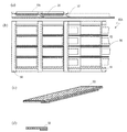
- FIG. 2 is a schematic cross-sectional view taken along line 1C-1C.
- A) And (b) is a typical top view of OLED display panel 10A and 10B obtained by the manufacturing method of the OLED display apparatus by embodiment of this invention. It is a perspective view which shows typically the structural example of the line beam irradiation apparatus 1000 used for manufacture of the OLED display apparatus by embodiment of this invention.
- (A) is sectional drawing which shows typically the process of peeling the polyimide film 14 from the panel board
- (b) is the heat
- (A) And (b) is a schematic diagram which shows the LLO process in the manufacturing method of the OLED display apparatus by embodiment of this invention. It is a schematic diagram which shows the other LLO process in the manufacturing method of the OLED display apparatus by embodiment of this invention. It is an optical image of a polyimide film after irradiating with laser beams with different energy densities.
- FIG. 2 is an optical image showing a state (left) in which the prototype OLED display panel is peeled from the glass substrate, and (c) is an optical image showing a light emission state of the prototype OLED display panel.
- A) And (b) is a schematic diagram which shows 42 A of spacer members.
- FIG. (A)-(c) is a figure for demonstrating the spacer member 50.
- FIG. (A)-(d) is a figure for demonstrating the spacer member 50A.
- (A) And (b) is a figure for demonstrating the spacer member 50B.
- 2 is a cross-sectional view schematically showing a top emission type OLED display panel 200.
- FIG. 1A and 1B are schematic plan views of multi-panel panel substrates 10a and 10b obtained in the manufacturing process of the OLED display device according to the embodiment of the present invention.
- FIG. 1C is a schematic cross-sectional view taken along line 1C-1C in FIG.
- a plurality of OLED display panel sections 20 are formed on the heat-resistant polymer film 14 formed on the support substrate 12.
- membrane 14 as the heat resistant polymer film 14 is demonstrated.
- the support substrate 12 only needs to sufficiently transmit light for peeling the heat-resistant polymer film 14 and have stable heat resistance and mechanical properties (including dimensional stability).
- the heat resistant polymer film 14 is preferably polyimide from the viewpoints of flexibility, mechanical strength, heat resistance, chemical resistance, etc., but is not limited thereto.
- the characteristics of the semiconductor layer used in the OLED display panel unit 20 tend to become better as the deposition temperature, the growth temperature of the semiconductor layer, or the annealing temperature of the semiconductor layer once deposited increases. Therefore, it is preferable that the heat-resistant polymer film 14 has heat resistance such that the semiconductor layer can be heated to, for example, more than 400 ° C., preferably 450 ° C. or more.
- the thickness of the polyimide film 14 is, for example, 10 ⁇ m to 30 ⁇ m.
- the plurality of OLED display panel sections 20 are arranged in a matrix having a plurality of rows and a plurality of columns, as shown in FIG.
- the row direction and the column direction are arbitrary, but here, the horizontal direction (long side direction of the substrate) is defined as the row direction, and the vertical direction (short side direction of the substrate) is defined as the column direction.
- the arrangement pitch of the OLED display panel unit 20 is arbitrarily set. It can be appropriately set according to the size of the panel substrate 10 a and the size of the OLED display panel unit 20. For example, as shown in the panel substrate 10b shown in FIG. 1B, the interval between the OLED display panel portions 20 adjacent to each other in the row direction can be increased as compared with the arrangement of the panel substrates 10a shown in FIG. Good. For example, as will be described later, the panel substrate 10b shown in FIG. 1B can be subjected to a peeling process after mounting a drive circuit, for example.
- the OLED display panel unit 20 includes an element layer 22 on which TFTs and OLEDs are formed, a barrier layer 24 formed on the element layer 22, and an upper layer of the barrier layer 24. It has the sealing film 26 formed in this.
- the OLED display panel unit 20 those having a known configuration can be widely used.
- the thickness of the element layer 22 is, for example, 2 ⁇ m to 5 ⁇ m.
- the barrier layer 24 is formed of, for example, a silicon nitride insulating layer, an organic material layer, or a multilayer structure thereof, and the thickness of the barrier layer 24 is, for example, 2 ⁇ m to 20 ⁇ m.
- the sealing film 26 is made of, for example, PEN (polyethylene naphthalate) or PET (polyethylene terephthalate), and the thickness of the sealing film 26 is, for example, 20 ⁇ m to 100 ⁇ m.
- PEN polyethylene naphthalate
- PET polyethylene terephthalate
- the OLED display panel unit 20 is peeled off from the glass substrate 12 together with the polyimide film 14 and separated into, for example, an OLED display panel 10A shown in FIG.
- the OLED display panel 10A is mounted with a drive circuit (for example, a driver IC) as necessary to become an OLED display module.
- an OLED display module 10B is obtained by connecting an FPC (Flexible Printed Circuits) 32 on which a driver IC 34 is mounted to the OLED display panel 10A.
- the driver IC may be directly mounted on the OLED display panel 10A.
- the driver IC may be formed monolithically.
- the OLED display panel 10A and the OLED display module 10B are included and referred to as an OLED display device.
- the final form including the power supply circuit and the control circuit in the OLED display module and the casing is also referred to as the OLED display device.
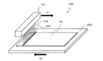
- FIG. 3 is a perspective view schematically showing a configuration example of the line beam irradiation apparatus 1000 used for manufacturing the OLED display device according to the embodiment of the present invention.
- the line beam irradiation apparatus 1000 includes a stage 200S and a line beam light source (laser head) 100 that irradiates the multi-panel panel substrate 10a placed on the stage 200S with the line beam 100L.
- a line beam light source laser head
- the line beam irradiation apparatus 1000 is a transfer apparatus (not shown) that moves at least one of the stage 200S and the line beam light source 100 so as to move the irradiation position 100P of the line beam 100L on the panel substrate 10a in a direction intersecting the line beam 100L. ). That is, the line beam light source 100 is moved in the direction indicated by the arrow LA, and / or the stage 200S is moved in the direction indicated by the arrow SA.
- the scanning speed of the line beam 100L on the panel substrate 10a is, for example, 1 cm / sec to 20 cm / sec (for example, 16 cm / sec).
- the line beam light source 100 for example, an excimer laser having a wavelength of 308 nm, a line beam 100L having a length of 750 mm, a width of 250 ⁇ m, and a laser energy density of 750 mJ / cm 2 is commercially available.
- a YAG laser (wavelength: 355 nm, line beam 100L length: 200 mm, width: 20 ⁇ m, laser energy density: 210 mJ / cm 2 ) can be used.
- FIG. 4A is a cross-sectional view schematically showing a process of peeling the polyimide film 14 from the panel substrate 10 a by the LLO method using the line beam irradiation apparatus 1000.
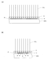
- FIG. 4B schematically shows the heat flow (dashed arrow) during line beam irradiation.
- the OLED display panel unit 20 of the panel substrate 10a and the gap between the OLED display panel unit 20 the region of the panel substrate 10a where the OLED display panel unit 20 does not exist).
- the polyimide film 14 cannot be uniformly peeled.
- the OLED display panel unit 20 is in contact with the stage 200S of the line beam irradiation apparatus 1000.
- the line beam 100L is simultaneously irradiated to the OLED display panel unit 20 of the panel substrate 10a and the gap portion of the OLED display panel unit 20 (region of the panel substrate 10a where the OLED display panel unit 20 does not exist).
- the temperature of the polyimide film 14 in the vicinity of the interface rapidly increases due to heat generated by the polyimide film 14 absorbing the line beam 100L condensed and irradiated on the interface between the polyimide film 14 and the glass substrate 12.
- the polyimide near the interface is decomposed, and the polyimide film 14 is peeled off from the glass substrate 12.
- the interface on the back surface side (upper side in the figure) of the OLED display panel unit 20 is relatively difficult to peel off, and the interface of the gap portion of the OLED display panel unit 20 is relatively easily peeled off. Accordingly, when the line beam 100L having an energy density capable of appropriately peeling the interface on the back surface side of the OLED display panel unit 20 is irradiated, the interface of the gap portion of the OLED display panel unit 20 cannot be peeled, or conversely, When the line beam 100L having an energy density capable of appropriately peeling the interface of the gap portion is irradiated, a large amount of ash (polyimide decomposition residue) is generated in the peeling portion on the back side of the OLED display panel unit 20. In addition, there is a possibility that the light emission characteristics of the OLED display panel are deteriorated due to heat generated by laser irradiation with high energy density.
- the polyimide film 14 and the glass substrate 12 are arranged from the glass substrate 12 side with the glass substrate 12 on the stage 200S and the OLED display panel unit 20 facing the stage 200S.
- the step of relatively moving the line beam 100L and the glass substrate 12 LLO step
- the OLED display panel unit from the interface between the polyimide film 14 and the glass substrate 12
- the heat release rate to 20 and the heat release rate from the interface between the polyimide film 14 and the glass substrate 12 to the gap portion of the OLED display panel unit 20 are made substantially equal.
- Whether or not the heat dissipation rates are substantially equal can be determined by whether or not a good peeling state can be obtained by irradiating the same line beam 100L.
- Good peeling state means that the polyimide film 14 does not remain on the glass substrate 12 and the amount of ash generated is sufficiently small.
- a specific example of the determination of the quality of the peeled state will be described later by showing an experimental example. Since the temperature rise due to the irradiation of the line beam 100L occurs in a very short time, it is difficult to obtain the heat dissipation rate by actually measuring the temperature change or the like.
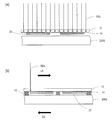
- the OLED display panel unit 20 is substantially insulated from the stage 200S. Specifically, as shown schematically in FIGS. 5A and 5B, the OLED display panel unit 20 is separated from the stage 200S. If it does so, it will mutually insulate with the air (atmosphere) which exists in the clearance gap between the OLED display panel part 20 and the stage 200S.
- a member having low thermal conductivity may be disposed in the gap.
- the low thermal conductivity member for example, a member formed of plastic can be used.
- the thermal conductivity is preferably 0.2 W / m ⁇ K or less, for example. Foamed plastic can also be used.
- heat radiation from the OLED display panel unit 20 may be suppressed by heating the stage 200S while the OLED display panel unit 20 is in contact with the stage 200S.
- the line beam 100L along the long side (side extending in the row direction) of the panel substrate 10a shown in FIG. 1A is parallel to the short side (side extending in the column direction).
- An example of moving (scanning) relative to is shown.
- a spacer member 42 extending in the row direction is arranged between the OLED display panel portions 20 adjacent in the column direction, and the OLED display panel portion 20 is separated from the stage 200S. Yes.
- the spacer member 42 may be formed using a material having relatively high thermal conductivity (for example, glass, metal (for example, stainless steel, aluminum)).
- the spacer member 42 extending in the row direction is provided between the OLED display panel portions 20 adjacent in the column direction, and the spacer member is not disposed between the OLED display panel portions 20 adjacent in the row direction.
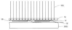
- the LLO process can be performed after the FPC 32 is mounted on the OLED display panel unit 20.
- the pitch in the row direction of the OLED display panel unit 20 can be increased unnecessarily. Absent.
- the spacer member 42 can be modified in various forms.
- the spacer member may have a plate shape having an opening at a position corresponding to the OLED display panel unit 20 and being thicker than the OLED display panel unit 20 (see, for example, FIG. 10).
- a spacer member in which walls are arranged in a lattice pattern in the gaps between the OLED display panel portions 20 arranged in a matrix can also be used.
- the spacer members may be arranged discretely.
- Stage 200S is made of stainless steel, and the feed rate is 5.175 cm / sec.
- a glass substrate and a PET film as a sealing film were used as a sample resembling the above-mentioned panel substrate.
- As the glass substrate AN100 manufactured by Asahi Glass, thickness 0.5 mm, 33 mm ⁇ 33 mm was used.
- Polyimide includes high heat resistant varnish material (Ube Industries' polyimide precursor solution U-Varnish-S (solvent NMP: N-methyl-2-pyrrolidone), solid content 18% by mass Using a slot coater, a film was formed so that the thickness after firing was 15 ⁇ m. Firing was performed using a hot-air circulating firing furnace at 400 to 500 ° C. for 0.1 to 1 hour.
- varnish material Ube Industries' polyimide precursor solution U-Varnish-S (solvent NMP: N-methyl-2-pyrrolidone)
- a PET (A4100 manufactured by Toyobo) thickness of 0.1 mm was used instead of the sealing film.
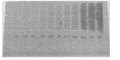
- FIG. 7 shows an optical image of the polyimide film after irradiation with laser beams having different energy densities using the above excimer laser.
- Energy density 120 mJ / cm 2 from the left, 130mJ / cm 2, 140mJ / cm 2, 150mJ / cm 2, 160mJ / cm 2, 170mJ / cm 2, 180mJ / cm 2, 190mJ / cm 2, 200mJ / cm 2 210 mJ / cm 2 and 220 mJ / cm 2 .
- the energy density was adjusted with an attenuator. The energy density when the attenuation by the attenuator is zero is the maximum energy density.
- the polyimide film When the energy density was 140 mJ / cm 2 or less, the polyimide film could not be peeled, and when the energy density was 150 mJ / cm 2 or more, the polyimide film could be peeled uniformly. Further, when the energy density was 170 mJ / cm 2 or more, the amount of ash generated increased as the energy density increased. In the optical image of FIG. 7, the color of the region irradiated with the laser light is dark due to the occurrence of ash. In particular, when the energy density was 200 mJ / cm 2 or more, the amount of ash generated was extremely large.
- the polyimide film can be uniformly peeled and the amount of ash generated can be sufficiently reduced. If the amount of ash generated is large, the cleaning process for removing ash takes time and the tact time becomes long.
- Table 1 shows the results of evaluating the possibility of peeling and the amount of ash generated by changing the energy density using a sample with a PET film attached to the center in the width direction of the glass substrate.
- ⁇ indicates an unpeeled region
- ⁇ indicates an unpeeled portion (point)
- ⁇ indicates that the entire surface has been completely peeled.
- the amount of ash generated was evaluated by the amount of ash that adheres to the gauze when the gauze was used to wipe off.
- ⁇ indicates that brown ash can be easily wiped off
- ⁇ indicates that it is extremely thinly attached to brown
- ⁇ indicates that gauze is not discolored.
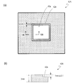
- the spacer member 42A shown in FIGS. 10A and 10B was used as a spacer member that supports the PET film in a state of being separated from the stage.
- An aluminum plate having a thickness of about 3 mm (the surface is anodized) has an opening 42a, and the sample was supported by a step 42s inside the opening 42a.
- the polyimide film can be peeled in all regions including the region where the PET film is pasted, and the ash is obtained. Can be reduced.
- the optimum energy density depends on the configuration and size of the panel substrate to be peeled, but the polyimide film can be peeled in the entire region including the OLED display panel, and the amount of ash generated is also high. There is an optimal energy density that can be reduced.
- FIG. 9A shows an optical image of the glass substrate (left) after peeling the polyimide film and the polyimide film (right) attached with PET in the above example under the condition of energy density of 170 mJ / cm 2. Show. As is clear from FIG. 9A, the polyimide film is completely peeled from the entire surface of the glass substrate, and the occurrence of ash is small.
- spacer member 42A shown in FIG. 10 was produced using a glass plate instead of the aluminum plate, and the result of the same peeling experiment using this spacer member was also good as in FIG. .
- the spacer member need not be a single member as exemplified above, and may be composed of a plurality of members, for example, a tray.
- the spacer member 50 can be used, for example, in the peeling process of the panel substrate 10a shown in FIG.
- the spacer member 50 includes a substrate 52 (for example, 375 ⁇ 620 ⁇ 0.5 mm) and two first spacers arranged along the long side (end side) of the substrate 52. 54 (for example, 620 ⁇ 20 ⁇ 2 mm) and three second spacers 56 (for example, 620 ⁇ 3 ⁇ 1.5 mm) extending in parallel with the first spacer 54.
- the substrate 52 is, for example, a glass substrate or an aluminum substrate.
- the first spacer 54 and the second spacer 56 are made of, for example, aluminum (the surface is anodized).
- the first spacer 54 has been processed to have a shape for mounting the panel substrate, and has a step portion 54s.
- the first spacer 54 supports the panel substrate with the step 54s and prevents the panel substrate from being displaced in the lateral direction.
- the second spacer 56 prevents the panel substrate from being bent downward due to its own weight, and keeps the height of the interface of the panel substrate irradiated with the laser light horizontally.
- the number of the second spacers 56 can be appropriately changed as necessary.
- the height of the second spacer 56 is set equal to the height of the step portion 54s of the first spacer 54 in order to match the height of the panel substrate from the stage.
- the height of the first spacer 54 is 2 mm and the thickness of the panel substrate is 0.5 mm
- the height of the stepped portion 54 s is required in order to match the height of the first spacer 54 and the height of the panel substrate.
- the length is 1.5 mm.
- the height of the second spacer 56 is 1.5 mm.
- the OLED display panel unit 20 peels off the panel substrate arranged in a matrix.
- the OLED display panel unit 20 has a plurality of OLED display panel units 20 arranged in one row.
- a plurality of panel substrates 10c can also be peeled together.
- the panel substrate 10c has an FPC 32 mounted on each OLED display panel section 20.
- the FPC 32 is mounted in the state of the panel substrate 10c having the plurality of OLED display panel sections 20, the throughput can be increased as compared with mounting the FPC 32 individually after the OLED display panel section 20 is peeled from the glass substrate.
- FIGS. 12A to 12D the structure and usage of the spacer member 50A will be described.
- the spacer member 50 ⁇ / b> A has a substrate 52, a first spacer 54, and a second spacer 56 like the spacer member 50 shown in FIG. 11A.
- the panel substrates 10c are arranged in a row with respect to the spacer member 50A.
- An FPC protection member 58 shown in FIGS. 12B and 12C is disposed between and both ends of two adjacent panel substrates 10c. The FPC protection member 58 protects the FPC from the laser light and adjusts the relative position of each panel substrate 10c.
- FIGS. 13A and 13B the structure and usage of the spacer member 50B will be described.
- the spacer member 50B has a tray shape having a plurality of cavities 50Ba each receiving the panel substrate 10c. As shown in FIG. 13B, the panel substrate 10c is disposed in the cavity 50Ba. At this time, the third spacer 50Bb is disposed as necessary. Of course, the third spacer 50Bb may be formed integrally with the spacer member 50B. Further, a support plate 57 may be disposed under the panel substrate 10c.
- the spacer member 50B, the third spacer 50Bb, and the support plate 57 are made of a low thermal conductivity material, for example, plastic.
- a spacer member 50B containing the panel substrate 10c in the cavity 50Ba is disposed on the stage.
- the spacer member 50B unlike the previous example, the OLED display panel unit 20 included in the panel substrate 10c comes into contact with the stage via the spacer member 50B, the third spacer 50Bb, and the support plate 57.
- the spacer member 50B, the third spacer 50Bb, and the support plate 57 are all made of a low thermal conductivity material (for example, thermal conductivity is 0.2 W / m ⁇ K or less), the OLED display panel unit 20 The same effect as that in the case of providing a gap between the stage and the stage can be obtained.
- the LLO process in the method for manufacturing an organic EL display device according to the embodiment of the present invention is not limited to the spacer member exemplified above, and various types of spacer members can be used.
- the organic EL display device manufactured by the manufacturing method according to the embodiment of the present invention may be, for example, a top emission type OLED display panel 200 shown in FIG. That is, the OLED display panel unit 20 in the previous embodiment may have the same structure as the OLED display panel 200 shown in FIG.
- FIG. 14 is a cross-sectional view schematically showing a top emission type OLED display panel 200.
- the OLED display panel 200 includes an active matrix substrate (TFT substrate) 210 and a sealing film 220, and includes a red pixel Pr, a green pixel Pg, and a blue pixel Pb.
- TFT substrate active matrix substrate
- sealing film 220 includes a red pixel Pr, a green pixel Pg, and a blue pixel Pb.
- the TFT substrate 210 includes an insulating substrate and a TFT circuit formed on the insulating substrate (both not shown).
- a flattening film 211 is provided in order to prevent the influence of the unevenness of the substrate when forming the TFT circuit.
- the planarizing film 211 is made of an organic insulating material.
- Lower electrodes 212R, 212G, and 212B are provided on the planarizing film 211.
- the lower electrodes 212R, 212G, and 212B are formed on the red pixel Pr, the green pixel Pg, and the blue pixel Pb, respectively.
- the lower electrodes 212R, 212G and 212B are connected to the TFT circuit and function as an anode.
- a bank 213 that covers the ends of the lower electrodes 212R, 212G, and 212B is provided between adjacent pixels.
- the bank 213 is made of an insulating material.
- Organic EL layers 214R, 214G, and 214B are provided on the lower electrodes 212R, 212G, and 212B of the red pixel Pr, the green pixel Pg, and the blue pixel Pb, respectively.
- Each of the organic EL layers 214R, 214G, and 214B has a stacked structure including a plurality of layers formed from an organic semiconductor material. This stacked structure includes, for example, a hole injection layer, a hole transport layer, a light emitting layer, an electron transport layer, and an electron injection layer in this order from the lower electrodes 212R, 212G, and 212B side.
- the organic EL layer 214R of the red pixel Pr includes a light emitting layer that emits red light.
- the organic EL layer 214G of the green pixel Pg includes a light emitting layer that emits green light.
- the organic EL layer 214B of the blue pixel Pb includes a light emitting layer that emits blue light.
- the upper electrode 215 is provided on the organic EL layers 214R, 214G, and 214B.
- the upper electrode 215 is formed using a transparent conductive material so as to be continuous over the entire display area (that is, common to the red pixel Pr, the green pixel Pg, and the blue pixel Pb), and functions as a cathode.
- a sealing layer 216 is provided on the upper electrode 215.
- the sealing layer 216 is formed of inorganic or organic, or an insulating material in which they are stacked.
- the above-described structure of the TFT substrate 210 is sealed with a sealing film 220 bonded to the TFT substrate 210 with a transparent resin layer 217.
- the organic EL display device manufactured by the manufacturing method according to the embodiment of the present invention is not limited to the above example, and may be various known organic EL display devices.
- a bottom emission type organic EL display device can be manufactured.
- the heat resistant polymer film 14 is preferably transparent to visible light, and a transparent polyimide film is preferably used.
- the organic EL display device manufactured by the manufacturing method according to the embodiment of the present invention is not limited to one having three independent pixels (OLED), and for example, emits white light and is colored by a color filter.
- An organic EL display device can also be manufactured.
- the present invention is used in a method for manufacturing an organic EL display device, particularly a flexible organic EL display device.
- 10a, 10b, 10c Panel substrate 12: Support substrate (glass substrate) 14: Heat-resistant polymer film (polyimide film) 20: OLED display panel unit 22: element layer 24: barrier layer 26: sealing film 32: FPC 34: Driver IC 42: Spacer member 42a: Opening 42s: Step 50: Spacer member 100: Line beam light source 100L: Line beam 100P: Irradiation position 200: OLED display panel 200S: Stage 1000: Line beam irradiation apparatus
Landscapes
- Engineering & Computer Science (AREA)
- Manufacturing & Machinery (AREA)
- Physics & Mathematics (AREA)
- Optics & Photonics (AREA)
- General Physics & Mathematics (AREA)
- Theoretical Computer Science (AREA)
- Plasma & Fusion (AREA)
- Mechanical Engineering (AREA)
- Electroluminescent Light Sources (AREA)
- Devices For Indicating Variable Information By Combining Individual Elements (AREA)
- Laser Beam Processing (AREA)
Abstract
実施形態による有機EL表示装置の製造方法は、支持基板(12)上に高分子膜(14)を形成する工程(a)と、高分子膜(14)の上に、複数の有機EL表示パネル部(20)を形成する工程(b)と、ステージ(200S)上で、有機EL表示パネル部(20)をステージ(200S)に向け、支持基板(12)側から、少なくとも高分子膜(14)と支持基板(12)との界面にラインビーム(100L)を照射しながら、ラインビーム(100L)と支持基板(12)とを相対的に移動させる工程であって、有機EL表示パネル部(20)をステージ(200S)から実質的に断熱した状態で行われる工程(c)とを包含する。
Description
本発明は、有機EL表示装置、特に、フレキシブルな有機EL表示装置の製造方法に関する。
有機EL(Electro Luminescence)表示装置が実用化され始めた。有機EL表示装置の特徴の1つにフレキシブルな表示装置が得られる点が挙げられる。有機EL表示装置は、画素ごとに少なくとも1つのOLED(Organic Light-Emitting Diode)と、各OLEDに供給される電流を制御する少なくとも1つのTFT(Thin Film Transistor)とを有する。以下、有機EL表示装置をOLED表示装置と呼ぶことにする。このようにOLEDごとにTFTなどのスイッチング素子を有するOLED表示装置は、アクティブマトリクス型OLED表示装置と呼ばれる。
フレキシブルOLED表示装置の基板としては、プラスチック基板、金属箔、高分子フィルムなどは検討されているが、液晶ディスプレイと同レベルの表示性能を得るためには前述のTFTを形成する必要があり、TFT製作工程における高温プロセスに対応するために耐熱性高分子フィルム(例えば、ポリイミドフィルム)が用いられている。しかしながら、フレキシブルな高分子フィルムを基板として用いて、高分子フィルム上にTFTやOLEDを形成することは寸法精度等の観点から極めて難しい。そこで、現在は、支持基板(典型的にはガラス基板)上に高分子フィルムを形成し、支持基板上の高分子フィルムの上に、TFTやOLEDを含む表示パネル部を形成した後、高分子フィルムを支持基板から剥離することによって、フレキシブルOLED表示パネルを得ている。この後、OLED表示パネルに必要に応じて、駆動回路を実装する等して、フレキシブルOLED表示装置が得られる。
高分子フィルムを支持基板から剥離する方法として、レーザリフトオフ(Laser Lift-Off:LLO)法が検討されている(例えば、特許文献1および2)。LLO法は、エキシマレーザまたはYAGレーザから出射された高出力のパルスレーザ光を高分子フィルムと支持基板との界面に集光、照射し、高分子フィルムを物理的または化学的に変化させ、高分子フィルムを支持基板から剥離する。パルスレーザ光は、断面形状が細長くライン状に延びた光ビームに成形される。このようなライン状の光ビームは「ラインビーム」と称されている。ラインビームの照射面における形状、すなわち光照射領域の形状は、例えば、長軸方向350mm、短軸方向1mm以下の矩形である。ラインビームを支持基板に対して短軸方向に相対的に移動させることによって、支持基板の全面にわたって高分子フィルムを連続して剥離することができる。
しかしながら、支持基板の全面にわたって高分子フィルムを均一に剥離することは容易ではない。特許文献1に記載の方法は、高分子フィルムの表示パネル部が形成される側とは反対側に、金属または金属酸化物を含む表面残留膜を形成している。表面残留膜と支持基板との間、または、表面残留膜と高分子フィルムとの間で剥離が起こる。
一方、特許文献2には、特許文献1に記載のように支持基板の全面にわたって剥離すると、フレキシブル表示パネルとして利用されない部分を含む状態で後工程を行う必要があるので煩雑であると記載されている。特許文献2は、剥離防止層を所定の位置に形成することによって、フレキシブル表示パネルとして利用される部分だけを選択的に剥離する方法を開示している。
しかしながら、特許文献1および2に記載の方法は、いずれもLLO法による剥離工程のための余分な層(表面残留膜または剥離防止層)を形成する必要があるので、コストを上昇させる。
本発明は従来よりも低コストでフレキシブルOLED表示装置を製造することができる方法を提供することを主な目的とする。
本発明の実施形態による有機EL表示装置の製造方法は、支持基板上に高分子膜を形成する工程(a)と、前記高分子膜の上に、複数の有機EL表示パネル部を形成する工程(b)と、ステージ上で、前記複数の有機EL表示パネル部を前記ステージに向け、前記支持基板側から、少なくとも前記高分子膜と前記支持基板との界面にラインビームを照射しながら、前記ラインビームと前記支持基板とを相対的に移動させる工程であって、前記複数の有機EL表示パネル部を前記ステージから実質的に断熱した状態で行われる工程(c)とを包含する。
ある実施形態において、前記工程(c)は、前記複数の有機EL表示パネル部が前記ステージから離間した状態で行われる。
ある実施形態において、前記複数の有機EL表示パネル部を形成する工程は、少なくとも1列に配列された複数の有機EL表示パネル部を形成する工程を含み、前記工程(c)の前に、前記少なくとも1列に配列された複数の有機EL表示パネル部に駆動回路を実装する工程をさらに含む。
ある実施形態において、前記工程(c)において、前記支持基板の前記複数の有機EL表示パネル部の間の領域と前記ステージとの間に配置されたスペーサ部材によって、前記複数の有機EL表示パネル部が前記ステージから離間した状態が維持される。
本発明の他の実施形態による有機EL表示装置の製造方法は、支持基板上に高分子膜を形成する工程(a)と、前記高分子膜の上に、複数の有機EL表示パネル部を形成する工程(b)と、ステージ上で、前記複数の有機EL表示パネル部を前記ステージに向け、前記支持基板側から、少なくとも前記高分子膜と前記支持基板との界面にラインビームを集光して照射しながら、前記ラインビームと前記支持基板とを相対的に移動させる工程であって、前記高分子膜と前記支持基板との界面から前記複数の有機EL表示パネル部への放熱速度と、前記高分子膜と前記支持基板との界面から前記複数の有機EL表示パネル部の間隙部分への放熱速度とを実質的に等しくした状態で行われる工程(c)とを包含する。
ある実施形態において、前記工程(c)は、前記ステージを加熱した状態で行われる。
本発明の実施形態によると、従来よりも低コストでフレキシブルOLED表示装置を製造することができる方法が提供される。
以下、図面を参照して本発明の実施形態によるOLED表示装置の製造方法を説明する。図1(a)および(b)に、本発明の実施形態によるOLED表示装置の製造過程で得られる、多面取りパネル基板10aおよび10bの模式的な平面図を示す。図1(c)は、図1(a)中の1C-1C線に沿った模式的な断面図である。
図1(c)に示す様に、支持基板12上に形成された耐熱性高分子膜14上に、複数のOLED表示パネル部20が形成されている。以下では、支持基板12として、ガラス基板12を用い、耐熱性高分子膜14としてポリイミド(芳香族ポリイミド)膜14を用いる例を説明する。一般に、支持基板12は、耐熱性高分子膜14を剥離するための光を十分に透過し、耐熱性および機械特性(寸法安定性を含む)が安定していればよい。耐熱性高分子膜14は、柔軟性、機械強度、耐熱性、耐薬品性等の観点からポリイミドが好ましいが、これに限られない。ただし、OLED表示パネル部20に用いられる半導体層の特性は、半導体層の堆積温度、成長温度、または一旦堆積された半導体層のアニール温度が高いほど優れる傾向にある。したがって、耐熱性高分子膜14は、半導体層が例えば400℃超、好ましくは450℃以上に加熱され得る耐熱性を有していることが好ましい。ポリイミド膜14の厚さは、例えば、10μm~30μmである。
複数のOLED表示パネル部20は、図1(a)に示す様に、複数の行および複数の列を有するマトリクス状に配列されている。行方向および列方向は任意であるが、ここでは、横方向(基板の長辺方向)を行方向とし、縦方向(基板の短辺方向)を列方向とする。
OLED表示パネル部20の配列ピッチは、任意に設定される。パネル基板10aのサイズおよびOLED表示パネル部20のサイズに応じて適宜設定され得る。例えば、図1(b)に示すパネル基板10bに示す様に、図1(a)に示すパネル基板10aの配列と比較して、行方向に隣接するOLED表示パネル部20の間隔を広げてもよい。例えば、図1(b)に示すパネル基板10bは、後述するように、例えば、駆動回路を実装した後に、剥離工程を行うことができる。
OLED表示パネル部20は、図1(c)に模式的に示す様に、TFTやOLEDが形成された素子層22と、素子層22の上に形成されたバリア層24およびバリア層24の上に形成された封止フィルム26を有している。OLED表示パネル部20としては公知の構成を有するものを広く用いることができる。素子層22の厚さは、例えば、2μm~5μmである。バリア層24は、例えば、窒化シリコン系絶縁層または有機物層またはそれらの多層構造で形成されており、バリア層24の厚さは、例えば、2μm~20μmである。封止フィルム26は、例えば、PEN(polyethylene naphthalate)、またはPET(polyethylene terephthalate)で形成されており、封止フィルム26の厚さは、例えば、20μm~100μmである。OLED表示パネル部20の構成例は、後に図14を参照して簡単に説明する。
OLED表示パネル部20は、後に説明するように、ポリイミド膜14とともにガラス基板12から剥離され、分離され、例えば、図2(a)に示すOLED表示パネル10Aとなる。OLED表示パネル10Aは、必要に応じて、駆動回路(例えばドライバIC)が実装され、OLED表示モジュールとなる。
例えば、図2(b)に示す様に、OLED表示パネル10Aに、ドライバIC34が実装されたFPC(Flexible Printed Circuits)32を接続することによって、OLED表示モジュール10Bが得られる。もちろん、ドライバICをOLED表示パネル10Aに直接実装してもよい。また、OLED表示パネル部20の製造工程において、ドライバICをモノリシックに形成してもよい。本明細書では、OLED表示パネル10AおよびOLED表示モジュール10Bを包含してOLED表示装置という。もちろん、OLED表示モジュールに電源回路および制御回路、さらに筺体を含む最終的な形態もOLED表示装置という。
次に、図3を参照して、LLO法を説明する。図3は、本発明の実施形態によるOLED表示装置の製造に用いられるラインビーム照射装置1000の構成例を模式的に示す斜視図である。
ラインビーム照射装置1000は、ステージ200Sと、ステージ200S上に置かれた多面取りパネル基板10aをラインビーム100Lで照射するラインビーム光源(レーザヘッド)100とを備える。
ラインビーム照射装置1000は、パネル基板10a上におけるラインビーム100Lの照射位置100Pをラインビーム100Lに交差する方向に移動させるようにステージ200Sおよびラインビーム光源100の少なくとも一方を移動させる搬送装置(不図示)を備えている。すなわち、ラインビーム光源100を矢印LAで示す方向に移動させる、および/またはステージ200Sを矢印SAで示す方向に移動させる。パネル基板10a上におけるラインビーム100Lの走査速度は、例えば、1cm/sec~20cm/sec(例えば16cm/sec)である。ラインビーム光源100として、例えば、波長308nmのエキシマレーザで、ラインビーム100Lの長さが750mm、幅が250μm、レーザエネルギー密度が750mJ/cm2であるエキシマレーザが市販されている。また、YAGレーザ(波長:355nm、ラインビーム100Lの長さ:200mm、幅:20μm、レーザエネルギー密度:210mJ/cm2)を用いることができる。
図4(a)および(b)を参照して、本発明の実施形態によって解決される課題を説明する。図4(a)は、ラインビーム照射装置1000を用いてLLO法によって、パネル基板10aからポリイミド膜14を剥離する工程を模式的に示す断面図である。図4(b)は、ラインビーム照射時における熱の流れ(破線矢印)を模式的に示したものである。後に実験例を示して説明するように、従来の方法では、パネル基板10aのOLED表示パネル部20と、OLED表示パネル部20の間隙部分(OLED表示パネル部20が存在しないパネル基板10aの領域)とで、均一にポリイミド膜14を剥離できないという問題があった。
従来は、図4(a)に示すように、OLED表示パネル部20をラインビーム照射装置1000のステージ200Sに接触させた状態で行っていた。ラインビーム100Lは、パネル基板10aのOLED表示パネル部20と、OLED表示パネル部20の間隙部分(OLED表示パネル部20が存在しないパネル基板10aの領域)とに同時に照射される。そうすると、ポリイミド膜14とガラス基板12との界面に集光、照射されたラインビーム100Lをポリイミド膜14が吸収することによって生じる熱によって、界面付近のポリイミド膜14の温度が急激に上昇する。その結果、界面付近のポリイミドが分解され、ガラス基板12からポリイミド膜14が剥がれる。
このとき、図4(b)に模式的に示す様に、界面付近で発生した熱の一部は、OLED表示パネル部20に伝達され、さらにはステージ200Sに伝達される(図中の破線矢印参照)。一方、OLED表示パネル部20の間隙部分には、OLED表示パネル部20が存在せず、ポリイミド膜14しか存在しない(バリア膜等は存在し得るがここでは説明の簡単のためにポリイミド膜14だけが存在することにする。)ので、ポリイミド膜14の界面で発生した熱は放熱され難い。その結果、OLED表示パネル部20の裏面側(図中上側)の界面は相対的に剥離され難く、OLED表示パネル部20の間隙部分の界面は相対的に剥離されやすくなる。したがって、OLED表示パネル部20の裏面側の界面を適切に剥離できるエネルギー密度のラインビーム100Lを照射すると、OLED表示パネル部20の間隙部分の界面を剥離できない、あるいは逆に、OLED表示パネル部20の間隙部分の界面を適切に剥離できるエネルギー密度のラインビーム100Lを照射すると、OLED表示パネル部20の裏面側の剥離部分に、多くのアッシュ(ポリイミドの分解残渣)が生成されることが起こる。また、高エネルギー密度のレーザ照射に伴う発熱により、OLED表示パネルの発光特性が低下する現象が生じる可能性がある。
本発明の実施形態による有機EL表示装置の製造方法においては、ガラス基板12をステージ200S上で、OLED表示パネル部20をステージ200Sに向け、ガラス基板12側から、少なくともポリイミド膜14とガラス基板12との界面にラインビーム100Lを照射しながら、ラインビーム100Lとガラス基板12とを相対的に移動させる工程(LLO工程)を行うとき、ポリイミド膜14とガラス基板12との界面からOLED表示パネル部20への放熱速度と、ポリイミド膜14とガラス基板12との界面からOLED表示パネル部20の間隙部分への放熱速度とを実質的に等しくする。放熱速度が実質的に等しいか否かは、同じラインビーム100Lを照射することによって、良好な剥離状態が得られるか否かで判定され得る。剥離状態が良好であるとは、ガラス基板12にポリイミド膜14が残っておらず、かつ、アッシュの発生量が十分に少ないことをいう。剥離状態の良否の判定の具体例は後に実験例を示して説明する。ラインビーム100Lの照射による温度の上昇は極めて短時間に起こるので、温度変化等を実測することによって、放熱速度を求めることは難しい。
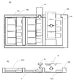
例えば、OLED表示パネル部20をステージ200Sから実質的に断熱した状態で行う。具体的には、図5(a)および(b)に模式的に示す様に、OLED表示パネル部20がステージ200Sから離間した状態で行う。そうすると、OLED表示パネル部20とステージ200Sとの間隙に存在する空気(大気)によって互いに断熱される。間隙に低熱伝導性の部材を配置してもよい。低熱伝導性の部材として、例えば、プラスチックで形成された部材を用いることができる。熱伝導率は、例えば、0.2W/m・K以下であることが好ましい。発泡プラスチックを用いることもできる。また、OLED表示パネル部20がステージ200Sに接触した状態で、ステージ200Sを加熱することによって、OLED表示パネル部20からの放熱を抑制してもよい。
図5(a)および(b)は、図1(a)に示したパネル基板10aの長辺(行方向に延びる辺)に沿ったラインビーム100Lを短辺(列方向に延びる辺)に平行に相対的に移動させる(走査する)例を示している。図5(b)に示すように、列方向に隣接するOLED表示パネル部20の間に行方向に延びるスペーサ部材42を配置し、OLED表示パネル部20がステージ200Sから離間した状態を実現している。スペーサ部材42は、熱伝導率が比較的高い材料(例えば、ガラス、金属(例えば、ステンレス鋼、アルミニウム)を用いて形成してもよい。
上述したように、列方向に隣接するOLED表示パネル部20の間に行方向に延びるスペーサ部材42を設け、行方向に隣接するOLED表示パネル部20の間にはスペーサ部材を配置しない構成を採用すると、例えば、図6に模式的に示す様に、OLED表示パネル部20にFPC32を実装した後で、LLO工程を行うことができる。このとき、図6に示すように、行方向に隣接するOLED表示パネル部20の下にFPC32を配置することができるので、OLED表示パネル部20の行方向のピッチを不必要に大きくすることがない。
スペーサ部材42は、種々の形態に改変され得る。スペーサ部材は、例えば、OLED表示パネル部20に対応する位置に開口部を有し、OLED表示パネル部20よりも厚いプレート状であってもよい(例えば、図10参照)。また、マトリクス状に配列されたOLED表示パネル部20の間隙に壁が格子状に配置されたスペーサ部材を用いることもできる。さらに、スペーサ部材を離散的に配置してもよい。
次に、実験例を説明する。
LLO工程には、波長が308nmのエキシマレーザ(JSW社製の装置C300)を用いた。エキシマレーザのパルスの条件は、以下の通りである。
発振周波数:300Hz
レーザの照射面積:750mm×345μm(25.9cm2)
最大エネルギー密度:235mJ/cm2
オーバーラップ率:50%
発振周波数:300Hz
レーザの照射面積:750mm×345μm(25.9cm2)
最大エネルギー密度:235mJ/cm2
オーバーラップ率:50%
ステージ200Sは、ステンレス製で、送り速度は5.175cm/secである。
上述のパネル基板に見立てたサンプルとして、ガラス基板と封止フィルムとしてPETのフィルムとを用いた。
ガラス基板としては、旭硝子製のAN100、厚さ0.5mm、33mm×33mmを用いた。
ポリイミドとしては、高耐熱性ワニス材料(宇部興産製のポリイミド前駆体溶液U-ワニス-S(溶媒NMP:N-メチル-2-ピロリドン (N-methyl-2-pyrrolidone))、ソリッドコンテンツ18質量%))を用いて、スロットコータを用いて、焼成後の厚さが15μmとなるように成膜した。焼成は、熱風循環式焼成炉を用いて、400℃~500℃、0.1時間~1時間、行った。
封止フィルムの代わりに、PET(東洋紡製のA4100)厚さ0.1mmを用いた。
まず、図7を参照して、ガラス基板からポリイミド膜を剥離するための最適エネルギー密度を検討した結果を説明する。図7は、上記のエキシマレーザを用いて、エネルギー密度が異なるレーザ光を照射した後のポリイミド膜の光学像を示す。エネルギー密度は、左から120mJ/cm2、130mJ/cm2、140mJ/cm2、150mJ/cm2、160mJ/cm2、170mJ/cm2、180mJ/cm2、190mJ/cm2、200mJ/cm2、210mJ/cm2、220mJ/cm2であった。エネルギー密度はアッテネータによって調節した。アッテネータによる減衰がゼロの時のエネルギー密度が、上記の最大エネルギー密度である。
エネルギー密度が140mJ/cm2以下ではポリイミド膜を剥離できず、150mJ/cm2以上のエネルギー密度のとき、ポリイミド膜を均一に剥離することができた。また、エネルギー密度が170mJ/cm2以上になると、エネルギー密度の増大とともにアッシュの発生量が増加した。図7の光学像において、レーザ光が照射された領域の色が濃くなっているのは、アッシュの発生による。特に、エネルギー密度が200mJ/cm2以上では、アッシュの発生量がきわめて多かった。このことからわかるように、エネルギー密度を適切な範囲に制御すれば、ポリイミド膜を均一に剥離し、かつ、アッシュの発生量を十分に少なくすることができる。なお、アッシュの発生量が多いと、アッシュを除去するための洗浄工程に時間がかかり、タクトタイムが長くなる。
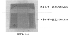
次に、OLED表示パネル部20に見立てて、ガラス基板の幅方向の中央に粘着剤を用いてPETフィルムを貼り付けた試料について、レーザ照射を行った。このとき、PETフィルムがステージに接触するように配置した。照射開始時のエネルギー密度を150mJ/cm2とし、短時間、レーザ照射を中断後、途中でエネルギー密度を170mJ/cm2に増大させた。レーザ照射後のポリイミド膜の光学像を図8に示す。
図8の結果から、エネルギー密度が150mJ/cm2では、PETフィルムを貼った領域(OLED表示パネル部を模擬した領域)のポリイミド膜を剥離できないことがわかった。また、エネルギー密度が150mJ/cm2で剥離することができた領域は、図7の場合(左から4本目)よりもアッシュの発生量が多かった。エネルギー密度を150mJ/cm2から170mJ/cm2に増大させると、増大直後には剥離できない領域が一部に生じたが、その後は、PETフィルムを貼った領域を含む全ての領域でポリイミド膜を剥離することができた。これらの実験結果から、図4を参照して説明したメカニズムで剥離不良が発生していると考えた。
ガラス基板の幅方向の中央にPETフィルムを貼った試料を用いて、エネルギー密度を変えて、剥離の可否、およびアッシュの発生量を評価した結果を表1に示す。剥離の程度の評価結果において、×は、未剥離領域あり、△は未剥離箇所(点)あり、○は全面にわたって完全に剥離出来たことを示す。アッシュの発生量の程度は、ガーゼを用いて拭き取った際にガーゼに付着するアッシュの量で評価した。アッシュの発生量の評価結果において、×は、容易に茶色のアッシュが拭き取れる程度、△は、極薄く茶色に付着する程度、○は、ガーゼが変色しない程度であったことを示す。
なお、実施例において、PETフィルムをステージから離間した状態で支持するスペーサ部材として、図10(a)および(b)に示すスペーサ部材42Aを用いた。厚さが約3mmのアルミニウム板(表面はアルマイト処理)に開口部42aを有しており、開口部42aの内側の段差部42sで試料を支持した。

表1の結果から分かるように、今回の試料では、エネルギー密度が170mJ/cm2であれば、PETフィルムを貼った領域を含む全ての領域でポリイミド膜を剥離することが可能で、かつ、アッシュの発生量も少なくできる。もちろん、最適なエネルギー密度は、剥離対象となるパネル基板の構成や大きさに依存するが、OLED表示パネル部を含む全領域でポリイミド膜を剥離することが可能で、かつ、アッシュの発生量も少なくできる最適なエネルギー密度が存在する。
図9(a)に上記実施例において、エネルギー密度が170mJ/cm2の条件で、ポリイミド膜を剥離した後のガラス基板(左)およびPETが貼り付けられたポリイミド膜(右)の光学像を示す。図9(a)から明らかなように、ポリイミド膜はガラス基板から全面にわたって完全に剥離されており、かつ、アッシュの発生も少ない。
ポリイミド膜上にOLED表示パネル部を作製し、封止用PETフィルム(バリアフィルム)を貼り合せた試作品を用いて、同様の実験を行った。図9(b)に示すように、図9(a)と同様に、アッシュの発生が少なく、且つ均一に剥離することができた。また、図9(c)に示すように、ガラス基板から剥離したOLED表示パネルは問題無く発光し、剥離によるダメージもなく、良好な発光が確認された。
また、図10に示したスペーサ部材42Aをアルミニウム板に代えてガラス板を用いて作製し、このスペーサ部材を用いて同様の剥離実験を行った結果も、図9と同様に、良好であった。
以下、図11から図14を参照して、スペーサ部材の例を説明する。なお、スペーサ部材は、先に例示したような単一の部材である必要はなく、複数の部材から構成されてもよく、例えば、トレイを含んでもよい。
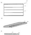
図11(a)~(c)を参照して、スペーサ部材50の構造および使用形態を説明する。スペーサ部材50は、例えば、図1(a)に示したパネル基板10aの剥離工程に用いられ得る。
図11(a)に示す様に、スペーサ部材50は、基板52(例えば、375×620×0.5mm)と、基板52の長辺(端辺)に沿って配置された2つの第1スペーサ54(例えば、620×20×2mm)と、第1スペーサ54と平行に延びる3本の第2スペーサ56(例えば、620×3×1.5mm)とを有している。基板52は、例えば、ガラス基板またはアルミニウム基板である。第1スペーサ54および第2スペーサ56は、例えばアルミニウム(表面はアルマイト処理)で作製される。
第1スペーサ54は、図11(b)に示す様に、パネル基板を載せるための形状加工がなされており段差部54sを有している。第1スペーサ54は、段差部54sでパネル基板を支持するとともに、横方向へのパネル基板の位置ずれを防止する。第2スペーサ56は、パネル基板の自重による下方向へのたわみを防止し、レーザ光が照射されるパネル基板の界面の高さを水平に保持する。第2スペーサ56の本数は、必要に応じて適宜変更され得る。第2スペーサ56の高さは、ステージからのパネル基板の高さを合せるために、第1スペーサ54の段差部54sの高さと等しく設定される。例えば、第1スペーサ54の高さを2mmとし、パネル基板の厚さを0.5mmとすると、第1スペーサ54の高さとパネル基板の高さを一致されるためには、段差部54sの高さは1.5mmとなる。このとき、第2スペーサ56の高さは1.5mmになる。
上記では、OLED表示パネル部20がマトリクス状に配列されたパネル基板を剥離する例を説明したが、例えば、図12に示すように、1列に配列された複数のOLED表示パネル部20を有するパネル基板10cを複数枚まとめて、剥離することもできる。
パネル基板10cは、各OLED表示パネル部20に対して、FPC32が実装されている。複数のOLED表示パネル部20を有するパネル基板10cの状態で、FPC32を実装すると、OLED表示パネル部20をガラス基板から剥離した後に、個別にFPC32を実装するよりもスループットを高めることができる。
図12(a)~(d)を参照して、スペーサ部材50Aの構造および使用形態を説明する。
スペーサ部材50Aは図12(b)に示すように、図11(a)に示したスペーサ部材50と同様に、基板52と、第1スペーサ54と、第2スペーサ56とを有している。スペーサ部材50Aに対して、パネル基板10cを一列ずつ配置する。隣接する2つのパネル基板10cの間および両端には、図12(b)および(c)に示すFPC保護部材58を配置する。FPC保護部材58は、レーザ光からFPCを保護するとともに、各パネル基板10cの相対位置を調整する。
図13(a)および(b)を参照して、スペーサ部材50Bの構造および使用形態を説明する。
スペーサ部材50Bは、それぞれがパネル基板10cを受容する複数のキャビティ50Baを有するトレイ形状である。図13(b)に示すように、パネル基板10cをキャビティ50Baに配置する。このとき、必要に応じて、第3スペーサ50Bbを配置する。もちろん、第3スペーサ50Bbは、スペーサ部材50Bと一体に形成されてもよい。また、パネル基板10cの下に支持板57を配置してもよい。スペーサ部材50B、第3スペーサ50Bbおよび支持板57は、低熱伝導性の材料、例えばプラスチックで形成される。
パネル基板10cをキャビティ50Baに収容したスペーサ部材50Bがステージ上に配置される。スペーサ部材50Bを用いると、先の例とは異なり、パネル基板10cが有するOLED表示パネル部20が、スペーサ部材50B、第3スペーサ50Bbおよび支持板57を介してステージと接触する。しかしながら、スペーサ部材50B、第3スペーサ50Bbおよび支持板57はいずれも低熱伝性の材料(例えば、熱伝導率が0.2W/m・K以下)で形成されているので、OLED表示パネル部20とステージとの間に空隙を設ける場合と同様の効果を得ることができる。
本発明の実施形態による有機EL表示装置の製造方法におけるLLO工程には、上記に例示したスペーサ部材に限らずれ、種々の形態のスペーサ部材を用いることができる。
また、本発明の実施形態による製造方法で製造される有機EL表示装置は、例えば、図14に示すトップエミッション方式のOLED表示パネル200であり得る。すなわち、先の実施形態におけるOLED表示パネル部20は、図14に示すOLED表示パネル200と同じ構造を有し得る。
図14は、トップエミッション方式のOLED表示パネル200を模式的に示す断面図である。
図14に示すように、OLED表示パネル200は、アクティブマトリクス基板(TFT基板)210および封止フィルム220を備え、赤画素Pr、緑画素Pgおよび青画素Pbを有する。
TFT基板210は、絶縁基板と、絶縁基板上に形成されたTFT回路とを含む(いずれも不図示)。TFT回路形成時、基板の凹凸の影響を防ぐために、平坦化膜211が設けられている。平坦化膜211は、有機絶縁材料から形成されている。
平坦化膜211上に、下部電極212R、212Gおよび212Bが設けられている。下部電極212R、212Gおよび212Bは、赤画素Pr、緑画素Pgおよび青画素Pbにそれぞれ形成されている。下部電極212R、212Gおよび212Bは、TFT回路に接続されており、陽極として機能する。隣接する画素間に、下部電極212R、212Gおよび212Bの端部を覆うバンク213が設けられている。バンク213は、絶縁材料から形成されている。
赤画素Pr、緑画素Pgおよび青画素Pbの下部電極212R、212Gおよび212B上に、有機EL層214R、214Gおよび214Bがそれぞれ設けられている。有機EL層214R、214Gおよび214Bのそれぞれは、有機半導体材料から形成された複数の層を含む積層構造を有する。この積層構造は、例えば、下部電極212R、212Gおよび212B側から、ホール注入層、ホール輸送層、発光層、電子輸送層および電子注入層をこの順で含んでいる。赤画素Prの有機EL層214Rは、赤色光を発する発光層を含む。緑画素Pgの有機EL層214Gは、緑色光を発する発光層を含む。青画素Pbの有機EL層214Bは、青色光を発する発光層を含む。
有機EL層214R、214Gおよび214B上に、上部電極215が設けられている。上部電極215は、透明導電材料を用いて表示領域全体にわたって連続するように(つまり赤画素Pr、緑画素Pgおよび青画素Pbに共通に)形成されており、陰極として機能する。上部電極215上に、封止層216が設けられている。封止層216は、無機または有機、またはそれらを積層した絶縁材料から形成されている。
TFT基板210の上述した構造は、TFT基板210に対して透明樹脂層217によって接着された封止フィルム220によって封止されている。
本発明の実施形態による製造方法で製造される有機EL表示装置は、上記の例に限られず、種々の公知の有機EL表示装置であり得る。例えば、ボトムエミッション方式の有機EL表示装置を製造することもできる。このとき、耐熱性高分子膜14は、可視光に対して透明であることが好ましく、透明ポリイミド膜を用いることが好ましい。また、本発明の実施形態による製造方法で製造される有機EL表示装置は、3色独立した画素(OLED)を有するものに限られず、例えば、白色を発光し、カラーフィルタでカラー化するタイプの有機EL表示装置を製造することもできる。
本発明は、有機EL表示装置、特に、フレキシブルな有機EL表示装置の製造方法に用いられる。
10a、10b、10c :パネル基板
12 :支持基板(ガラス基板)
14 :耐熱性高分子膜(ポリイミド膜)
20 :OLED表示パネル部
22 :素子層
24 :バリア層
26 :封止フィルム
32 :FPC
34 :ドライバIC
42 :スペーサ部材
42a :開口部
42s :段差部
50 :スペーサ部材
100 :ラインビーム光源
100L :ラインビーム
100P :照射位置
200 :OLED表示パネル
200S :ステージ
1000 :ラインビーム照射装置
12 :支持基板(ガラス基板)
14 :耐熱性高分子膜(ポリイミド膜)
20 :OLED表示パネル部
22 :素子層
24 :バリア層
26 :封止フィルム
32 :FPC
34 :ドライバIC
42 :スペーサ部材
42a :開口部
42s :段差部
50 :スペーサ部材
100 :ラインビーム光源
100L :ラインビーム
100P :照射位置
200 :OLED表示パネル
200S :ステージ
1000 :ラインビーム照射装置
Claims (6)
- 支持基板上に高分子膜を形成する工程(a)と、
前記高分子膜の上に、複数の有機EL表示パネル部を形成する工程(b)と、
ステージ上で、前記複数の有機EL表示パネル部を前記ステージに向け、前記支持基板側から、少なくとも前記高分子膜と前記支持基板との界面にラインビームを照射しながら、前記ラインビームと前記支持基板とを相対的に移動させる工程であって、前記複数の有機EL表示パネル部を前記ステージから実質的に断熱した状態で行われる工程(c)と
を包含する、有機EL表示装置の製造方法。 - 前記工程(c)は、前記複数の有機EL表示パネル部が前記ステージから離間した状態で行われる、請求項1に記載の有機EL表示装置の製造方法。
- 前記複数の有機EL表示パネル部を形成する工程は、少なくとも1列に配列された複数の有機EL表示パネル部を形成する工程を含み、
前記工程(c)の前に、前記少なくとも1列に配列された複数の有機EL表示パネル部に駆動回路を実装する工程をさらに含む、請求項1または2に記載の有機EL表示装置の製造方法。 - 前記工程(c)において、前記支持基板の前記複数の有機EL表示パネル部の間の領域と前記ステージとの間に配置されたスペーサ部材によって、前記複数の有機EL表示パネル部が前記ステージから離間した状態が維持される、請求項1から3のいずれかに記載の有機EL表示装置の製造方法。
- 支持基板上に高分子膜を形成する工程(a)と、
前記高分子膜の上に、複数の有機EL表示パネル部を形成する工程(b)と、
ステージ上で、前記複数の有機EL表示パネル部を前記ステージに向け、前記支持基板側から、少なくとも前記高分子膜と前記支持基板との界面にラインビームを集光して照射しながら、前記ラインビームと前記支持基板とを相対的に移動させる工程であって、前記高分子膜と前記支持基板との界面から前記複数の有機EL表示パネル部への放熱速度と、前記高分子膜と前記支持基板との界面から前記複数の有機EL表示パネル部の間隙部分への放熱速度とを実質的に等しくした状態で行われる工程(c)と
を包含する、有機EL表示装置の製造方法。 - 前記工程(c)は、前記ステージを加熱した状態で行われる、請求項5に記載の有機EL表示装置の製造方法。
Priority Applications (3)
| Application Number | Priority Date | Filing Date | Title |
|---|---|---|---|
| CN201680076648.4A CN108432345B (zh) | 2015-12-28 | 2016-07-22 | 有机el显示装置的制造方法 |
| JP2017558853A JP6410282B2 (ja) | 2015-12-28 | 2016-07-22 | 有機el表示装置の製造方法 |
| US16/066,590 US11158841B2 (en) | 2015-12-28 | 2016-07-22 | Method for manufacturing organic el display device |
Applications Claiming Priority (2)
| Application Number | Priority Date | Filing Date | Title |
|---|---|---|---|
| JP2015-256464 | 2015-12-28 | ||
| JP2015256464 | 2015-12-28 |
Publications (2)
| Publication Number | Publication Date |
|---|---|
| WO2017115484A1 true WO2017115484A1 (ja) | 2017-07-06 |
| WO2017115484A8 WO2017115484A8 (ja) | 2017-09-14 |
Family
ID=59227378
Family Applications (1)
| Application Number | Title | Priority Date | Filing Date |
|---|---|---|---|
| PCT/JP2016/071574 Ceased WO2017115484A1 (ja) | 2015-12-28 | 2016-07-22 | 有機el表示装置の製造方法 |
Country Status (5)
| Country | Link |
|---|---|
| US (1) | US11158841B2 (ja) |
| JP (1) | JP6410282B2 (ja) |
| CN (1) | CN108432345B (ja) |
| TW (1) | TW201725768A (ja) |
| WO (1) | WO2017115484A1 (ja) |
Cited By (5)
| Publication number | Priority date | Publication date | Assignee | Title |
|---|---|---|---|---|
| JP6334080B1 (ja) * | 2017-10-26 | 2018-05-30 | 堺ディスプレイプロダクト株式会社 | フレキシブルoledデバイスの製造方法および製造装置 |
| JP6334079B1 (ja) * | 2017-10-26 | 2018-05-30 | 堺ディスプレイプロダクト株式会社 | フレキシブルoledデバイスの製造方法および製造装置 |
| WO2019215832A1 (ja) * | 2018-05-09 | 2019-11-14 | 堺ディスプレイプロダクト株式会社 | フレキシブル発光デバイスの製造方法および製造装置 |
| WO2019215835A1 (ja) * | 2018-05-09 | 2019-11-14 | 堺ディスプレイプロダクト株式会社 | フレキシブル発光デバイスの製造方法および製造装置 |
| US11127726B2 (en) | 2018-05-09 | 2021-09-21 | Sakai Display Products Corporation | Method and device for manufacturing flexible light emission device |
Citations (5)
| Publication number | Priority date | Publication date | Assignee | Title |
|---|---|---|---|---|
| JP2003163337A (ja) * | 2001-08-10 | 2003-06-06 | Semiconductor Energy Lab Co Ltd | 剥離方法および半導体装置の作製方法 |
| JP2003229548A (ja) * | 2001-11-30 | 2003-08-15 | Semiconductor Energy Lab Co Ltd | 乗物、表示装置、および半導体装置の作製方法 |
| US20130011969A1 (en) * | 2011-07-04 | 2013-01-10 | Industrial Technology Research Institute | Method for fabricating the flexible electronic device |
| US20140327006A1 (en) * | 2013-05-01 | 2014-11-06 | Au Optronics Corporation | Active Device Substrate and Manufacturing Method Thereof |
| JP2015083373A (ja) * | 2013-09-18 | 2015-04-30 | 株式会社半導体エネルギー研究所 | 積層体の作製装置 |
Family Cites Families (16)
| Publication number | Priority date | Publication date | Assignee | Title |
|---|---|---|---|---|
| JP4202065B2 (ja) | 2001-07-27 | 2008-12-24 | トヨタ自動車株式会社 | リベット品質モニタリング装置、リベット品質モニタリング方法およびリベット品質モニタリングプログラム |
| TW554398B (en) | 2001-08-10 | 2003-09-21 | Semiconductor Energy Lab | Method of peeling off and method of manufacturing semiconductor device |
| TWI258317B (en) * | 2002-01-25 | 2006-07-11 | Semiconductor Energy Lab | A display device and method for manufacturing thereof |
| TWI307612B (en) * | 2005-04-27 | 2009-03-11 | Sony Corp | Transfer method and transfer apparatus |
| US7820531B2 (en) * | 2007-10-15 | 2010-10-26 | Sony Corporation | Method of manufacturing semiconductor device, method of manufacturing display apparatus, apparatus of manufacturing semiconductor device, and display apparatus |
| KR101307549B1 (ko) * | 2007-12-31 | 2013-09-12 | 엘지디스플레이 주식회사 | 유기전계발광표시장치의 제조방법 |
| JP5244680B2 (ja) * | 2008-04-14 | 2013-07-24 | 株式会社半導体エネルギー研究所 | 発光装置の作製方法 |
| KR101318442B1 (ko) * | 2008-04-25 | 2013-10-16 | 엘지디스플레이 주식회사 | 유기전계발광표시장치의 제조방법 |
| KR101579872B1 (ko) * | 2008-04-29 | 2015-12-24 | 삼성디스플레이 주식회사 | 전사 기판, 이의 제조방법 및 유기 전계 발광소자의제조방법 |
| KR101149433B1 (ko) | 2009-08-28 | 2012-05-22 | 삼성모바일디스플레이주식회사 | 플렉서블 표시 장치 및 그 제조 방법 |
| JP2014048619A (ja) | 2012-09-04 | 2014-03-17 | Panasonic Corp | フレキシブルデバイスの製造方法 |
| KR102015400B1 (ko) * | 2012-11-29 | 2019-10-22 | 삼성디스플레이 주식회사 | 캐리어 기판의 박리 장치, 캐리어 기판의 박리 방법 및 표시 장치의 제조 방법 |
| KR20140102518A (ko) * | 2013-02-14 | 2014-08-22 | 삼성디스플레이 주식회사 | 도너 필름, 이의 제조 방법 및 이를 이용한 유기 발광 표시 장치의 제조 방법 |
| KR20150007740A (ko) * | 2013-07-12 | 2015-01-21 | 삼성디스플레이 주식회사 | 전사용 도너 기판 및 유기 발광 표시 장치의 제조 방법 |
| TWI561325B (en) * | 2014-08-01 | 2016-12-11 | Au Optronics Corp | Display module manufacturing method and display module |
| KR102180647B1 (ko) * | 2014-09-03 | 2020-11-23 | 삼성디스플레이 주식회사 | 광학 마스크 |
-
2016
- 2016-07-22 CN CN201680076648.4A patent/CN108432345B/zh active Active
- 2016-07-22 US US16/066,590 patent/US11158841B2/en active Active
- 2016-07-22 JP JP2017558853A patent/JP6410282B2/ja active Active
- 2016-07-22 WO PCT/JP2016/071574 patent/WO2017115484A1/ja not_active Ceased
- 2016-07-27 TW TW105123732A patent/TW201725768A/zh unknown
Patent Citations (5)
| Publication number | Priority date | Publication date | Assignee | Title |
|---|---|---|---|---|
| JP2003163337A (ja) * | 2001-08-10 | 2003-06-06 | Semiconductor Energy Lab Co Ltd | 剥離方法および半導体装置の作製方法 |
| JP2003229548A (ja) * | 2001-11-30 | 2003-08-15 | Semiconductor Energy Lab Co Ltd | 乗物、表示装置、および半導体装置の作製方法 |
| US20130011969A1 (en) * | 2011-07-04 | 2013-01-10 | Industrial Technology Research Institute | Method for fabricating the flexible electronic device |
| US20140327006A1 (en) * | 2013-05-01 | 2014-11-06 | Au Optronics Corporation | Active Device Substrate and Manufacturing Method Thereof |
| JP2015083373A (ja) * | 2013-09-18 | 2015-04-30 | 株式会社半導体エネルギー研究所 | 積層体の作製装置 |
Cited By (14)
| Publication number | Priority date | Publication date | Assignee | Title |
|---|---|---|---|---|
| US10497887B1 (en) | 2017-10-26 | 2019-12-03 | Sakai Display Products Corporation | Method and apparatus for producing flexible OLED device |
| JP6334080B1 (ja) * | 2017-10-26 | 2018-05-30 | 堺ディスプレイプロダクト株式会社 | フレキシブルoledデバイスの製造方法および製造装置 |
| WO2019082360A1 (ja) * | 2017-10-26 | 2019-05-02 | 堺ディスプレイプロダクト株式会社 | フレキシブルoledデバイスの製造方法および製造装置 |
| WO2019082359A1 (ja) * | 2017-10-26 | 2019-05-02 | 堺ディスプレイプロダクト株式会社 | フレキシブルoledデバイスの製造方法および製造装置 |
| US10505155B1 (en) | 2017-10-26 | 2019-12-10 | Sakai Display Products Corporation | Method and apparatus for producing flexible OLED device |
| JP6334079B1 (ja) * | 2017-10-26 | 2018-05-30 | 堺ディスプレイプロダクト株式会社 | フレキシブルoledデバイスの製造方法および製造装置 |
| US11127726B2 (en) | 2018-05-09 | 2021-09-21 | Sakai Display Products Corporation | Method and device for manufacturing flexible light emission device |
| JPWO2019215832A1 (ja) * | 2018-05-09 | 2020-05-28 | 堺ディスプレイプロダクト株式会社 | フレキシブル発光デバイスの製造方法および製造装置 |
| WO2019215835A1 (ja) * | 2018-05-09 | 2019-11-14 | 堺ディスプレイプロダクト株式会社 | フレキシブル発光デバイスの製造方法および製造装置 |
| JPWO2019215835A1 (ja) * | 2018-05-09 | 2020-05-28 | 堺ディスプレイプロダクト株式会社 | フレキシブル発光デバイスの製造方法および製造装置 |
| CN112042272A (zh) * | 2018-05-09 | 2020-12-04 | 堺显示器制品株式会社 | 柔性发光器件的制造方法以及制造装置 |
| US11101258B2 (en) | 2018-05-09 | 2021-08-24 | Sakai Display Products Corporation | Method and apparatus for manufacturing flexible light-emitting device |
| WO2019215832A1 (ja) * | 2018-05-09 | 2019-11-14 | 堺ディスプレイプロダクト株式会社 | フレキシブル発光デバイスの製造方法および製造装置 |
| US11158804B2 (en) | 2018-05-09 | 2021-10-26 | Sakai Display Products Corporation | Method and apparatus for manufacturing flexible light emitting device |
Also Published As
| Publication number | Publication date |
|---|---|
| US11158841B2 (en) | 2021-10-26 |
| JPWO2017115484A1 (ja) | 2018-12-06 |
| CN108432345A (zh) | 2018-08-21 |
| TW201725768A (zh) | 2017-07-16 |
| JP6410282B2 (ja) | 2018-10-24 |
| WO2017115484A8 (ja) | 2017-09-14 |
| CN108432345B (zh) | 2020-02-28 |
| US20190044096A1 (en) | 2019-02-07 |
Similar Documents
| Publication | Publication Date | Title |
|---|---|---|
| JP6410282B2 (ja) | 有機el表示装置の製造方法 | |
| US9276212B2 (en) | Method of cutting flexible display device and method of fabricating flexible display device using the same | |
| TWI259803B (en) | Method of manufacturing color filter substrate, method of manufacturing electro-optical device, electro-optical device, and electronic apparatus | |
| CN102683379B (zh) | 柔性显示装置及其制造方法 | |
| JP6674592B1 (ja) | フレキシブル発光デバイスの製造方法および製造装置 | |
| JP6333502B1 (ja) | フレキシブルoledデバイスの製造方法および製造装置 | |
| JP6334078B1 (ja) | フレキシブルoledデバイスの製造方法および製造装置 | |
| JP2017058509A (ja) | 表示装置の製造方法、および、表示装置 | |
| JP6694558B2 (ja) | フレキシブル発光デバイスの製造方法および製造装置 | |
| CN112042271A (zh) | 柔性发光器件的制造方法以及制造装置 | |
| JP6670425B1 (ja) | フレキシブル発光デバイスの製造方法および製造装置 | |
| JP6692003B2 (ja) | フレキシブル発光デバイスの製造方法および製造装置 | |
| JP6674593B1 (ja) | フレキシブル発光デバイスの製造方法および製造装置 | |
| JPWO2014049904A1 (ja) | El表示装置の製造方法、el表示装置の製造に用いられる転写基板 | |
| JPWO2019215829A1 (ja) | フレキシブル発光デバイスの製造方法および製造装置 | |
| JPH10233286A (ja) | 有機エレクトロルミネッセンス表示装置 | |
| WO2021005798A1 (ja) | フレキシブル発光デバイスの製造方法及び支持基板 | |
| JP6535122B2 (ja) | フレキシブルoledデバイスの製造方法および製造装置 | |
| KR101335639B1 (ko) | 레이저 결정화 장치 및 이를 이용한 실리콘 결정화 방법 | |
| JP2010160943A (ja) | 有機elパネル製造用転写装置、有機elパネルの製造方法および有機elパネル製造用担持体 | |
| JP2018137403A (ja) | 表示装置の製造方法および光照射装置 | |
| JP2020115238A (ja) | フレキシブル発光デバイスの製造方法および製造装置 | |
| WO2021005796A1 (ja) | フレキシブル発光デバイス、その製造方法及び支持基板 |
Legal Events
| Date | Code | Title | Description |
|---|---|---|---|
| 121 | Ep: the epo has been informed by wipo that ep was designated in this application |
Ref document number: 16881464 Country of ref document: EP Kind code of ref document: A1 |
|
| ENP | Entry into the national phase |
Ref document number: 2017558853 Country of ref document: JP Kind code of ref document: A |
|
| NENP | Non-entry into the national phase |
Ref country code: DE |
|
| 122 | Ep: pct application non-entry in european phase |
Ref document number: 16881464 Country of ref document: EP Kind code of ref document: A1 |