WO2017110432A1 - レギュレーションプレート、これを備えためっき装置及びめっき方法 - Google Patents
レギュレーションプレート、これを備えためっき装置及びめっき方法 Download PDFInfo
- Publication number
- WO2017110432A1 WO2017110432A1 PCT/JP2016/086021 JP2016086021W WO2017110432A1 WO 2017110432 A1 WO2017110432 A1 WO 2017110432A1 JP 2016086021 W JP2016086021 W JP 2016086021W WO 2017110432 A1 WO2017110432 A1 WO 2017110432A1
- Authority
- WO
- WIPO (PCT)
- Prior art keywords
- opening
- substrate
- blades
- diameter
- regulation plate
- Prior art date
- Legal status (The legal status is an assumption and is not a legal conclusion. Google has not performed a legal analysis and makes no representation as to the accuracy of the status listed.)
- Ceased
Links
Images










Classifications
-
- C—CHEMISTRY; METALLURGY
- C25—ELECTROLYTIC OR ELECTROPHORETIC PROCESSES; APPARATUS THEREFOR
- C25D—PROCESSES FOR THE ELECTROLYTIC OR ELECTROPHORETIC PRODUCTION OF COATINGS; ELECTROFORMING; APPARATUS THEREFOR
- C25D17/00—Constructional parts, or assemblies thereof, of cells for electrolytic coating
- C25D17/001—Apparatus specially adapted for electrolytic coating of wafers, e.g. semiconductors or solar cells
-
- C—CHEMISTRY; METALLURGY
- C25—ELECTROLYTIC OR ELECTROPHORETIC PROCESSES; APPARATUS THEREFOR
- C25D—PROCESSES FOR THE ELECTROLYTIC OR ELECTROPHORETIC PRODUCTION OF COATINGS; ELECTROFORMING; APPARATUS THEREFOR
- C25D17/00—Constructional parts, or assemblies thereof, of cells for electrolytic coating
- C25D17/007—Current directing devices
-
- C—CHEMISTRY; METALLURGY
- C25—ELECTROLYTIC OR ELECTROPHORETIC PROCESSES; APPARATUS THEREFOR
- C25D—PROCESSES FOR THE ELECTROLYTIC OR ELECTROPHORETIC PRODUCTION OF COATINGS; ELECTROFORMING; APPARATUS THEREFOR
- C25D17/00—Constructional parts, or assemblies thereof, of cells for electrolytic coating
- C25D17/008—Current shielding devices
-
- C—CHEMISTRY; METALLURGY
- C25—ELECTROLYTIC OR ELECTROPHORETIC PROCESSES; APPARATUS THEREFOR
- C25D—PROCESSES FOR THE ELECTROLYTIC OR ELECTROPHORETIC PRODUCTION OF COATINGS; ELECTROFORMING; APPARATUS THEREFOR
- C25D17/00—Constructional parts, or assemblies thereof, of cells for electrolytic coating
- C25D17/10—Electrodes, e.g. composition, counter electrode
-
- C—CHEMISTRY; METALLURGY
- C25—ELECTROLYTIC OR ELECTROPHORETIC PROCESSES; APPARATUS THEREFOR
- C25D—PROCESSES FOR THE ELECTROLYTIC OR ELECTROPHORETIC PRODUCTION OF COATINGS; ELECTROFORMING; APPARATUS THEREFOR
- C25D17/00—Constructional parts, or assemblies thereof, of cells for electrolytic coating
- C25D17/10—Electrodes, e.g. composition, counter electrode
- C25D17/12—Shape or form
-
- C—CHEMISTRY; METALLURGY
- C25—ELECTROLYTIC OR ELECTROPHORETIC PROCESSES; APPARATUS THEREFOR
- C25D—PROCESSES FOR THE ELECTROLYTIC OR ELECTROPHORETIC PRODUCTION OF COATINGS; ELECTROFORMING; APPARATUS THEREFOR
- C25D21/00—Processes for servicing or operating cells for electrolytic coating
- C25D21/12—Process control or regulation
-
- C—CHEMISTRY; METALLURGY
- C25—ELECTROLYTIC OR ELECTROPHORETIC PROCESSES; APPARATUS THEREFOR
- C25D—PROCESSES FOR THE ELECTROLYTIC OR ELECTROPHORETIC PRODUCTION OF COATINGS; ELECTROFORMING; APPARATUS THEREFOR
- C25D5/00—Electroplating characterised by the process; Pretreatment or after-treatment of workpieces
- C25D5/02—Electroplating of selected surface areas
- C25D5/022—Electroplating of selected surface areas using masking means
-
- C—CHEMISTRY; METALLURGY
- C25—ELECTROLYTIC OR ELECTROPHORETIC PROCESSES; APPARATUS THEREFOR
- C25D—PROCESSES FOR THE ELECTROLYTIC OR ELECTROPHORETIC PRODUCTION OF COATINGS; ELECTROFORMING; APPARATUS THEREFOR
- C25D5/00—Electroplating characterised by the process; Pretreatment or after-treatment of workpieces
- C25D5/04—Electroplating with moving electrodes
-
- H—ELECTRICITY
- H10—SEMICONDUCTOR DEVICES; ELECTRIC SOLID-STATE DEVICES NOT OTHERWISE PROVIDED FOR
- H10P—GENERIC PROCESSES OR APPARATUS FOR THE MANUFACTURE OR TREATMENT OF DEVICES COVERED BY CLASS H10
- H10P14/00—Formation of materials, e.g. in the shape of layers or pillars
- H10P14/40—Formation of materials, e.g. in the shape of layers or pillars of conductive or resistive materials
- H10P14/46—Formation of materials, e.g. in the shape of layers or pillars of conductive or resistive materials using a liquid
-
- H—ELECTRICITY
- H10—SEMICONDUCTOR DEVICES; ELECTRIC SOLID-STATE DEVICES NOT OTHERWISE PROVIDED FOR
- H10P—GENERIC PROCESSES OR APPARATUS FOR THE MANUFACTURE OR TREATMENT OF DEVICES COVERED BY CLASS H10
- H10P14/00—Formation of materials, e.g. in the shape of layers or pillars
- H10P14/40—Formation of materials, e.g. in the shape of layers or pillars of conductive or resistive materials
- H10P14/46—Formation of materials, e.g. in the shape of layers or pillars of conductive or resistive materials using a liquid
- H10P14/47—Electrolytic deposition, i.e. electroplating; Electroless plating
Definitions
- the present invention relates to a regulation plate, a plating apparatus provided with the regulation plate, and a plating method.
- bumps that form wiring in fine wiring grooves, holes, or resist openings provided on the surface of a substrate such as a semiconductor wafer, or that are electrically connected to package electrodes or the like on the surface of the substrate Forming an electrode).
- a method for forming the wiring and the bump for example, an electrolytic plating method, a vapor deposition method, a printing method, a ball bump method and the like are known.
- electrolytic plating methods that can be miniaturized and have relatively stable performance have come to be used.
- a seed layer (feeding layer) having a low electrical resistance is formed on the surface of the barrier metal provided in the wiring groove, hole, or resist opening on the substrate.
- a plated film grows on the surface of the seed layer.
- a seed layer having a thinner film thickness has been used. As the seed layer becomes thinner, the electrical resistance (sheet resistance) of the seed layer increases.
- a substrate to be plated has an electrical contact at the periphery. For this reason, a current corresponding to a combined resistance of the electrical resistance value of the plating solution and the electrical resistance value of the seed layer from the central part of the substrate to the electrical contact flows through the central part of the substrate. On the other hand, a current corresponding to the electric resistance value of the plating solution flows almost at the peripheral edge of the substrate (near the electrical contact). That is, the current hardly flows through the central portion of the substrate by the amount of the electrical resistance of the seed layer from the central portion of the substrate to the electrical contact. This phenomenon of current concentration at the peripheral edge of the substrate is called a terminal effect.
- a substrate having a relatively thin seed layer has a relatively large electrical resistance value of the seed layer from the center of the substrate to the electrical contact. For this reason, when plating is performed on a substrate having a relatively thin seed layer, the terminal effect becomes significant. As a result, the plating rate at the center of the substrate is reduced, the film thickness of the plating film at the center of the substrate is thinner than the plating film at the periphery of the substrate, and the in-plane uniformity of the film thickness is reduced.
- a plating apparatus in which an adjustment plate for adjusting a potential distribution between an anode and a substrate is installed between the anode and the substrate (see Patent Document 1).
- the influence of the terminal effect varies depending on the thickness of the substrate seed layer. Specifically, as described above, when the seed layer is relatively thin, the sheet resistance is relatively large, so that the influence of the terminal effect appears remarkably. On the other hand, when the seed layer is relatively thick, the sheet resistance is relatively small, so the influence of the terminal effect is relatively small.
- the effect of the terminal effect can vary depending on not only the film thickness of the seed layer but also other factors.
- the resist opening ratio of the substrate the proportion of the area of the region bordered by the resist outer edge that is not covered by the resist (the opening portion of the resist)
- the area of the plating film is relatively large.
- the plating film is formed on the substrate, the current easily flows through the central portion of the substrate due to the formed plating film.
- the electric resistance value from the central portion of the substrate to the electrical contact is reduced, so that the influence of the terminal effect is gradually reduced.
- the resist opening ratio of the substrate when the resist opening ratio of the substrate is relatively low, the area of the plating film formed on the substrate is relatively small. For this reason, when the resist opening ratio of the substrate is relatively low, even if a plating film is formed on the substrate, the electrical resistance from the center of the substrate to the electrical contact is larger than when the resist opening ratio of the substrate is relatively high. The change in value is small and the effect of the terminal effect remains large.
- the influence of the terminal effect is smaller than when the electric resistance value of the plating solution for treating the substrate is relatively small.
- the electric resistance value of the plating solution is R1
- the electric resistance value of the seed layer from the central portion of the substrate to the electric contact is R2
- the central portion of the substrate corresponds to the combined resistance value (R1 + R2).
- Current flows.
- a current corresponding to the electric resistance value R1 of the plating solution almost flows through the peripheral edge of the substrate (near the electrical contact). Therefore, if the electric resistance value R1 is increased, the influence of the electric resistance value R2 on the current flowing through the center of the substrate is reduced, and the influence of the terminal effect is reduced.
- the influence of the terminal effect varies depending on the characteristics of the substrate and the conditions for processing the substrate. For this reason, when sequentially plating a plurality of substrates having different effects of the terminal effect in a single plating apparatus, in order to suppress a decrease in in-plane uniformity of the film thickness due to the terminal effect, the characteristics of each substrate and It is necessary to adjust the electric field applied to the substrate in accordance with conditions for processing the substrate.
- the adjustment plate as described in Patent Document 1, an adjustment plate suitable for the characteristics of the substrate and the conditions for processing the substrate You have to prepare several.
- the present invention has been made in view of the above problems, and one of its purposes is to suppress a reduction in in-plane uniformity due to the influence of the terminal effect when plating on a plurality of substrates having different characteristics and processing conditions. It is providing the regulation plate which can be performed, the plating apparatus provided with this, and the plating method.
- a regulation plate for adjusting the current between the anode and the substrate to be plated.
- the regulation plate includes a plate main body portion having an edge portion forming a first opening through which a current passes, a plurality of first blades for reducing the diameter of the first opening, and the plurality of first blades.
- a first moving mechanism that translates in the radial direction of the first opening.
- the diameter of the opening of the regulation plate can be adjusted by narrowing the diameter of the opening with the first blade.
- the characteristics or processing conditions of the first substrate and the second substrate are different from each other, it is possible to suppress a decrease in in-plane uniformity due to the influence of the terminal effect.
- the film formation speed at the peripheral edge of the substrate can be suppressed by reducing the diameter of the opening of the regulation plate.
- In-plane uniformity of the substrate can be improved.
- the first blade is configured to move in translation, the plurality of first blades can move in the radial direction while maintaining the angular relationship with the other first blades. Therefore, compared to a case where a plurality of aperture blades rotate about a predetermined axis to reduce the diameter of the aperture as in the aperture mechanism of a camera, the perfect circular shape of the aperture formed by the first blade can be maintained. it can.
- the first moving mechanism includes a ring member arranged along the edge, and one of the ring member and the plurality of first blades is A slide long hole inclined with respect to the radial direction of the first opening is provided, and the other of the ring member and the plurality of first blades has a slide pin that slides through the slide long hole.
- the slide pin provided in the other of the ring member and the plurality of first blades slides through the slide long hole provided in one of the ring member and the plurality of first blades. Therefore, by rotating the ring member in the circumferential direction, the slide pin slides in the slide long hole, and the first blade can be moved in the radial direction of the opening.
- the first moving mechanism includes a blade pressing member fixed to the opposite side of the ring member of the plurality of first blades, and the blade pressing member and the plurality of the blade pressing members Any one of the first blades has a guide elongated hole formed in parallel with the translational movement direction of the first blade, and the other of the blade pressing member and the plurality of first blades is the guide elongated hole. It has a guide pin that slides.
- the guide pin provided in the other of the blade pressing member and the plurality of first blades slides through the guide long hole provided in either the blade pressing member or the plurality of first blades. . Therefore, when the plurality of first blades are moved by the moving mechanism, the first blades can be translated in a desired direction while preventing the plurality of first blades from rotating.
- the first moving mechanism includes a rotating member for rotating the ring member in a circumferential direction, and the rotating member is fixed to the ring member.
- the ring portion can be rotated in the circumferential direction by operating the lever portion by an actuator or manually. Since the ring portion is fixed to the ring member, the ring member rotates as the ring portion rotates. Thereby, the slide long hole or slide pin provided in the ring member slides with the slide pin or slide long hole provided in the plurality of first blades, and the plurality of first blades can be translated.
- either one of the plate main body part and the ring part has a support long hole formed along the rotation direction of the ring part, and the plate main body part and The other of the ring portions has a support pin that slidably engages with the support slot.
- the support pin provided on the other of the plate main body part and the ring part is slidably engaged with the support long hole provided on one of the plate main body part and the ring part.
- the ring portion is supported by the plate body portion by the support pin engaging with the support slot. Since the support long hole is formed along the rotation direction of the ring portion, the ring portion can be rotated by the support pin sliding on the support long hole.
- each of the plurality of first blades has an inner peripheral edge formed in an arc shape and overlaps with the other first blades to be substantially circular. Forming the inner periphery of
- the inner peripheral edges of the plurality of first blades can be maintained in a substantially circular shape.
- the regulation plate is disposed at a position displaced from the plurality of first blades in a direction perpendicular to the radial direction of the first opening, A plurality of second blades for reducing the diameter of the first opening; and a second moving mechanism that translates the plurality of second blades in a radial direction of the first opening.
- the regulation plate has an opening having a first diameter formed by the plurality of first blades and an opening having a second diameter formed by the plurality of second blades.
- a straight line connecting the centers of the openings formed by the plurality of first blades and the centers of the openings formed by the plurality of second blades is a radial direction of these openings.
- the first blade and the second blade are arranged so as to be orthogonal to each other.
- the first blade and the second blade are arranged so that the opening center formed by the first blade and the opening center formed by the second blade coincide with each other. Therefore, when positioning the regulation plate in the plating tank, there is no need to separately position the opening center formed by the plurality of first blades and the opening center formed by the plurality of second blades. For this reason, even if it is a case where high precision is calculated
- a regulation plate for adjusting the current between the anode and the substrate to be plated.
- the regulation plate includes a first plate body having a first edge forming a first opening through which a current passes, and a plurality of first blades for reducing the diameter of the first opening, And a second plate body having a second edge that forms a second opening through which the first opening passes and a plurality of second blades for reducing the diameter of the second opening.
- the first plate body portion so that a straight line connecting the centers of the openings formed by the plurality of first blades and the centers of the openings formed by the plurality of second blades is orthogonal to the radial direction of the openings.
- the second plate body is connected to each other.
- the regulation plate has an opening having a first diameter formed by the plurality of first blades and an opening having a second diameter formed by the plurality of second blades.
- the first blade and the second blade are arranged so that the opening center formed by the first blade and the opening center formed by the second blade coincide with each other. Therefore, when positioning the regulation plate in the plating tank, there is no need to separately position the opening center formed by the plurality of first blades and the opening center formed by the plurality of second blades. For this reason, even if it is a case where high precision is calculated
- an opening diameter formed by the plurality of first blades and an opening diameter formed by the plurality of second blades are independent from each other. And can be adjusted.
- the diameter of the opening defined by the plurality of first blades can be made different from the diameter of the opening defined by the plurality of second blades.
- the diameter of the opening defined by the blade close to the substrate is reduced, and the diameter of the opening defined by the blade far from the substrate is increased. Can be small.
- a plating apparatus includes an anode holder configured to hold an anode, a substrate holder disposed to face the anode holder and configured to hold a substrate, and is integrally attached to the anode holder.
- An anode mask having a second opening through which a current flowing between the anode and the substrate passes, and any one of the regulation plates, wherein the anode mask adjusts a diameter of the second opening.
- the diameter of the second opening of the anode mask can be adjusted for each of the first substrate and the second substrate.
- the characteristics or processing conditions of the first substrate and the second substrate are different from each other, it is possible to suppress a decrease in in-plane uniformity due to the influence of the terminal effect.
- the diameter of the first opening of the regulation plate is reduced, the film formation speed at the peripheral edge of the substrate can be suppressed. Therefore, by adjusting both the diameter of the first opening of the regulation plate and the diameter of the second opening of the anode mask, the in-plane uniformity of the substrate W can be further improved.
- a plating method includes a step of arranging an anode holder integrally provided with an anode mask having a first opening through which a current flowing between the anode and the substrate passes, and a substrate holder for holding the first substrate. And a regulation plate having a second opening and a third opening through which a current flowing between the anode and the substrate passes is disposed between the anode mask and the substrate.
- the It has a Kkisuru step.
- the diameter of the first opening of the anode mask can be adjusted for each of the first substrate and the second substrate.
- FIG. 6 is a rear view of a regulation plate having a minimum inner diameter opening. It is a front side perspective view of a regulation plate which has a plurality of 1st blades and a plurality of 2nd blades concerning other embodiments.
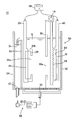
- FIG. 1 is a schematic sectional side view of a plating apparatus according to this embodiment.
- the plating apparatus 10 according to the present embodiment includes an anode holder 20 configured to hold the anode 21, a substrate holder 40 configured to hold the substrate W, the anode holder 20, and the substrate. And a plating tank 50 that houses the holder 40 therein.
- the plating tank 50 includes a plating treatment tank 52 that contains a plating solution Q containing an additive, a plating solution discharge tank 54 that receives and discharges the plating solution Q overflowed from the plating treatment tank 52, A partition wall 55 that partitions the plating treatment tank 52 and the plating solution discharge tank 54.
- the anode holder 20 holding the anode 21 and the substrate holder 40 holding the substrate W are immersed in the plating solution Q in the plating tank 52 so that the anode 21 and the surface to be plated W1 of the substrate W face each other.
- a voltage is applied to the anode 21 and the substrate W by the plating power source 59 in a state where the anode 21 and the substrate W are immersed in the plating solution Q of the plating treatment tank 52.
- the metal ions are reduced on the plated surface W1 of the substrate W, and a film is formed on the plated surface W1.
- the plating tank 52 has a plating solution supply port 56 for supplying the plating solution Q to the inside of the vessel.
- the plating solution discharge tank 54 has a plating solution discharge port 57 for discharging the plating solution Q overflowed from the plating treatment tank 52.
- the plating solution supply port 56 is disposed at the bottom of the plating treatment tank 52, and the plating solution discharge port 57 is disposed at the bottom of the plating solution discharge tank 54.
- the plating solution Q When the plating solution Q is supplied from the plating solution supply port 56 to the plating treatment tank 52, the plating solution Q overflows from the plating treatment tank 52 and flows into the plating solution discharge tank 54 over the partition wall 55.
- the plating solution Q flowing into the plating solution discharge tank 54 is discharged from the plating solution discharge port 57, and impurities are removed by a filter or the like included in the plating solution circulation device 58.
- the plating solution Q from which impurities have been removed is supplied to the plating treatment tank 52 through the plating solution supply port 56 by the plating solution circulation device 58.
- the anode holder 20 has an anode mask 25 for adjusting the electric field between the anode 21 and the substrate W.
- the anode mask 25 is a substantially plate-like member made of, for example, a dielectric material, and is provided on the front surface of the anode holder 20.
- the front surface of the anode holder 20 refers to the surface on the side facing the substrate holder 40. That is, the anode mask 25 is disposed between the anode 21 and the substrate holder 40.
- the anode mask 25 has an opening 25a (corresponding to an example of a second opening) through which a current flowing between the anode 21 and the substrate W passes in a substantially central portion.
- the diameter of the opening 25a is preferably smaller than the diameter of the anode 21.
- the anode mask 25 is configured such that the diameter of the opening 25a can be adjusted.
- the anode mask 25 has an anode mask attachment portion 25b for attaching the anode mask 25 to the anode holder 20 integrally on the outer periphery thereof.
- the position of the anode mask 25 may be between the anode holder 20 and the substrate holder 40, but is preferably closer to the anode holder 20 than an intermediate position between the anode holder 20 and the substrate holder 40. Further, for example, the anode mask 25 may be disposed on the front surface of the anode holder 20 without being attached to the anode holder 20.
- the relative position of the anode mask 25 with respect to the anode holder 20 is fixed, so that the position of the anode 21 and the position of the opening 25a are shifted. Can be prevented.
- the anode 21 held by the anode holder 20 is preferably an insoluble anode.
- the anode 21 is not dissolved even when the plating process proceeds, and the shape of the anode 21 does not change. For this reason, since the positional relationship (distance) between the anode mask 25 and the surface of the anode 21 does not change, the positional relationship between the anode mask 25 and the surface of the anode 21 changes, whereby the electric field between the anode 21 and the substrate W is changed. Can be prevented from changing.
- the plating apparatus 10 further includes a regulation plate 60 for adjusting the current between the anode 21 and the substrate W.
- the regulation plate 60 is a substantially plate-like member made of, for example, a dielectric material, and is disposed between the anode mask 25 and the substrate holder 40 (substrate W).
- the regulation plate 60 has an opening 60a (corresponding to an example of a first opening) through which a current flowing between the anode 21 and the substrate W passes.
- the diameter of the opening 60a is preferably smaller than the diameter of the substrate W.
- the regulation plate 60 is configured to be able to adjust the diameter of the opening 60a.
- the regulation plate 60 is preferably located closer to the substrate holder 40 than an intermediate position between the anode holder 20 and the substrate holder 40. By adjusting the diameter of the opening 60a of the regulation plate 60 as the regulation plate 60 is arranged closer to the substrate holder 40, the film thickness of the peripheral portion of the substrate W can be controlled more accurately.
- a paddle 18 for stirring the plating solution Q in the vicinity of the surface W1 to be plated of the substrate W is provided.
- the paddle 18 is a substantially rod-shaped member, and is provided in the plating treatment tank 52 so as to face the vertical direction.
- One end of the paddle 18 is fixed to the paddle driving device 19.
- the paddle 18 is horizontally moved along the to-be-plated surface W1 of the substrate W by the paddle driving device 19, whereby the plating solution Q is agitated.
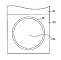
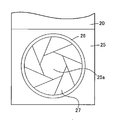
- FIG. 2 and 3 are schematic front views of the anode mask 25.
- FIG. FIG. 2 shows the anode mask 25 when the diameter of the opening 25a is relatively large.
- FIG. 3 shows the anode mask 25 when the diameter of the opening 25a is relatively small.
- the opening 25a of the anode mask 25 is smaller, the current flowing from the anode 21 to the substrate W is concentrated on the central portion of the surface W1 to be plated of the substrate W. Therefore, when the opening 25a is made small, the film thickness of the central portion of the surface W1 to be plated of the substrate W tends to increase.
- the anode mask 25 has a substantially annular edge 26.
- the diameter of the opening 25a of the anode mask 25 shown in FIG. 2 is the maximum. In this case, the diameter of the opening 25 a matches the inner diameter of the edge portion 26.
- the anode mask 25 has a plurality of aperture blades 27 (corresponding to an example of an adjusting mechanism) configured to be able to adjust the opening 25a.
- the diaphragm blades 27 cooperate to define the opening 25a.
- Each of the diaphragm blades 27 enlarges or reduces the diameter of the opening 25a (adjusts the diameter of the opening 25a) by the same structure as the diaphragm mechanism of the camera.
- the opening 25 a of the anode mask 25 shown in FIG. 3 is formed in a non-circular shape (for example, a polygonal shape) by the diaphragm blades 27.
- the diameter of the opening 25a in this case refers to the shortest distance between opposing sides of the polygon or the diameter of an inscribed circle.
- the diameter of the opening 25a can be defined by the diameter of a circle having an area equivalent to the opening area.
- the distance between the anode 21 and the surface of the diaphragm blade 27 facing the anode 21 is, for example, 0 mm or more and 8 mm or less.
- Each of the diaphragm blades 27 enlarges or reduces the diameter of the opening 25a manually, for example.
- Each of the diaphragm blades 27 may be configured to be driven using air pressure or an electric driving force.
- the adjusting mechanism using the diaphragm blades 27 has a feature that the opening 25a can be made variable in a relatively wide range. Further, when the substrate is circular, the opening 25a of the anode mask 25 is preferably circular. However, in the opening 25a having a variable diameter in a relatively wide range, maintaining a complete circle in the entire range from the minimum diameter to the maximum diameter of the opening 25a is accompanied by mechanical difficulties.
- the azimuth distribution of the electric field becomes uneven, and the plating film thickness distribution formed on the peripheral edge of the substrate W
- the shape of the opening may be transferred to
- the anode mask 25 is integrally attached to the anode holder 20
- a sufficient distance from the substrate can be obtained, and the influence on the plating film thickness distribution is maximized even when the opening is not completely circular. Can be suppressed.
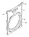
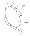
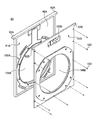
- FIG. 4 shows a front perspective view of the regulation plate 60 in a state where the diameter of the opening 60a is relatively large
- FIG. 5 shows a rear perspective view of the regulation plate 60 in a state where the diameter of the opening 60a is relatively large
- FIG. 6 is a front perspective view of the regulation plate 60 in a state where the diameter of the opening 60a is relatively small.
- the regulation plate 60 has a substantially plate-shaped plate body 61.
- the plate main body 61 has a pair of suspending portions 62 for suspending and suspending the regulation plate 60 on the edge of the plating bath 52 shown in FIG. Further, the plate main body 61 has an opening 60a at a substantially central portion thereof.
- the opening 60 a is formed by an opening adjusting portion 63 provided in the plate main body portion 61.
- a rotating member 100 that constitutes a part of the opening adjustment portion 63 is attached to the back side of the regulation plate 60.
- the regulation plate 60 includes a blade body 70 configured to reduce the diameter of the opening 60a. Details of the rotating member 100 and the blade body 70 will be described later.
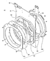
- FIG. 7 is an exploded perspective view of the regulation plate 60.
- the regulation plate 60 includes a plate body portion 61, a blade body 70, a ring member 80, a blade pressing member 90, a rotating member 100, and a protection member 110.
- the blade body 70, the ring member 80, the blade pressing member 90, the rotating member 100, and the protection member 110 constitute an opening adjustment unit 63.
- the regulation plate 60 has an edge portion 64 that forms an opening 60 a together with the plate body portion 61.
- the blade body 70 has a plurality of first blades 71 for reducing the diameter of the opening 60 a and is positioned on the front side of the edge portion 64 of the regulation plate 60.
- the front side of the regulation plate 60 refers to the surface facing the substrate holder 40 shown in FIG.
- the regulation plate 60 may be disposed in the plating treatment tank 52 of FIG. 1 so that the front side of the regulation plate 60 faces the anode holder 20 shown in FIG.
- the ring member 80 is configured to translate the plurality of first blades 71 in the radial direction of the opening 60a.
- the ring member 80 is disposed along the edge 64 of the regulation plate 60.
- the ring member 80 is disposed along the inner peripheral surface of the edge portion 64 of the regulation plate 60.
- the present invention is not limited thereto, and the ring member 80 may be disposed on the front side of the edge portion 64 of the regulation plate 60, for example.
- the blade pressing member 90 is disposed on the front side of the blade body 70 (the side opposite to the ring member 80).
- the rotating member 100 is disposed on the rear surface side of the plate body 61 and is coupled to the ring member 80 as will be described later.
- each member which comprises the regulation plate 60 is demonstrated in detail.
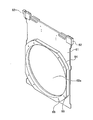
- FIG. 8 shows a front perspective view of the plate body 61
- FIG. 9 shows a rear perspective view of the plate body 61
- the plate main body 61 is a substantially plate-like member, and has an opening 60a at a substantially central portion thereof.
- An edge portion 64 having substantially the same opening as the opening 60 a is fixed to the front surface side of the plate main body portion 61.
- the edge portion 64 forms an opening 60 a together with the plate body portion 61.
- the plate main body 61 has a plurality of pin holes 65 for inserting support pins that slidably support the rotating member 100 on the rear surface side.
- the edge portion 64 has a plurality of screw holes 66 on the front side thereof for screwing screws for fixing the blade pressing member 90 and the protection member 110 together.
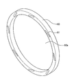
- FIG. 10 is a front perspective view of the ring member 80.
- the ring member 80 is disposed along the inner peripheral surface of the opening 60a of the plate main body 61 shown in FIGS. Therefore, the outer diameter of the ring member 80 is configured to approximately match the inner diameter of the edge portion 64 that forms the opening 60 a of the plate main body portion 61. For this reason, the inner diameter of the ring member 80 becomes the maximum inner diameter of the opening 60a.
- the ring member 80 (corresponding to an example of the first moving mechanism) has a plurality of slide long holes 81 on the front side thereof. In the present embodiment, eight slide long holes 81 corresponding to the number of first blades 71 constituting the blade body 70 are provided in the ring member 80.
- the slide long hole 81 may or may not penetrate through the ring member 80 toward the rear surface side.
- the slide long hole 81 is configured to be inclined with respect to the radial direction of the opening 60a.
- the slide elongated hole 81 is disposed so as to be inclined so that the longitudinal direction of the elongated hole does not face the center of the opening 60a.
- Each of the slide long holes 81 is provided in the ring member 80 so as to be rotationally symmetric with respect to the central axis of the opening 60a. In this embodiment, since eight slide long holes 81 are provided, each of the slide long holes 81 is eight-fold rotationally symmetric.
- FIG. 11 is a front perspective view of the rotating member 100.
- the rotating member 100 includes a ring part 101 and a plate-like lever part 102 attached to the ring part 101.
- the ring part 101 is fixed to the rear surface side of the ring member 80 shown in FIG.
- the inner diameter of the ring portion 101 is configured to substantially match the inner diameter of the ring member 80.
- the lever portion 102 is coupled to the outer peripheral portion of the ring portion 101, and the ring portion 101 rotates in the circumferential direction within the range of the swing angle by swinging the lever portion 102 in the circumferential direction of the ring portion 101.
- convex portions 104 are provided on the outer periphery of the ring portion 101, and support long holes 103 along the circumferential direction of the ring portion 101 are formed in each of the convex portions 104.
- the support elongated hole 103 is slidably supported by a support pin fixed to the pin hole 65 of the plate main body 61 shown in FIG.
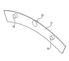
- FIG. 12 is a front perspective view of the first blade 71 constituting the blade body 70.
- the first blade 71 is a fan-shaped member having an inner peripheral edge formed in an arc shape.
- the first blade 71 overlaps with the other first blades 71 to form a substantially circular inner periphery of the blade body 70 as a whole.
- the blade body 70 is configured by the eight first blades 71, but the blade body 70 can be configured by any number of the first blades 71 without being limited thereto.
- a slide pin 72 configured to slide in the slide long hole 81 of the ring member 80 shown in FIG. 10 is provided on the rear surface side of the first blade 71.
- one slide pin 72 is provided on the first blade 71, but not limited thereto, two or more slide pins 72 may be provided on the first blade 71. In this case, it is necessary to match the number of the slide long holes 81 of the ring member 80 shown in FIG.
- a guide pin 73 configured to slide in a guide slot 91 of a blade pressing member 90 shown in FIG.
- the two guide pins 73 are provided on the first blade 71, but not limited to this, one or three or more guide pins 73 may be provided on the first blade 71.
- FIG. 13 is a front perspective view of the blade pressing member 90.
- the blade pressing member 90 is a substantially plate-like member, and an opening 60a is formed at a substantially central portion thereof.
- the diameter of the opening 60a of the blade pressing member 90 is substantially the same as the inner diameter of the ring member 80 shown in FIG.
- the blade pressing member 90 has a plurality of guide long holes 91.
- 16 guide elongated holes 91 are provided in the blade pressing member 90, and the two guide elongated holes 91 correspond to the two guide pins 73 of the first blade 71 shown in FIG.
- the number of guide elongated holes 91 can be changed as appropriate according to the number of guide pins 73.
- the guide slot 91 is formed in parallel with the translational movement direction of the first blade 71.
- the blade pressing member 90 has a plurality of screw holes 92. The position of the screw hole 66 and the position of the screw hole 92 formed in the edge portion 64 of the plate main body 61 shown in FIG. Can be fixed.
- the blade pressing member 90 is disposed so that the rear surface side is in contact with the front surface side of the blade body 70. Therefore, when the first blade 71 of the blade body 70 is translated in the radial direction of the opening 60 a, the first blade 71 is translated while being in contact with the blade pressing member 90.
- the blade pressing member 90 is preferably made of a low friction resin such as PTFE.
- FIG. 14 is a front perspective view of the protection member 110.
- the protection member 110 is a substantially plate-like member, and an opening 60a is formed at a substantially central portion thereof.
- the diameter of the opening 60a of the protection member 110 is substantially the same as the inner diameter of the ring member 80 shown in FIG.
- the protection member 110 is disposed on the front side of the blade pressing member 90.
- the protection member 110 has a plurality of screw holes 111.
- the position of the screw hole 66 shown in FIG. 8 and the position of the screw hole 92 shown in FIG. 13 and the position of the screw hole 111 are matched, and the screw is screwed to fix the protective member 110 to the plate main body 61. it can.
- the protection member 110 is made of, for example, vinyl chloride, and protects the front side of the blade pressing member 90.
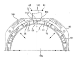
- FIG. 15 is a partial front view of the regulation plate 60 from the front side.
- the rotary member 100, the plurality of first blades 71, the blade pressing member 90, and the slide elongated holes 81 of the ring member 80 are shown in a transparent manner, and the other members are simplified in the drawing. Therefore, it is omitted.
- the plurality of first blades 71 are arranged so as to have overlapping portions 75 that partially overlap with the other first blades 71.
- the inner peripheral edges of the plurality of first blades 71 are formed in a substantially circular shape.
- the slide pins 72 of the plurality of first blades 71 are located in a substantially middle part of the slide long hole 81, and the guide pin 73 is located in a substantially middle part of the guide long hole 91.
- the inner diameters of the inner peripheral edges of the plurality of first blades 71 are smaller than the inner diameter of the opening 60 a of the regulation plate 60. Therefore, the plurality of first blades 71 reduce the inner diameter of the opening 60 a of the regulation plate 60.
- the ring member 80 (not shown) coupled to the ring portion 101 also rotates in the circumferential direction.
- the lever portion 102 moves in the direction of the arrow A1 (clockwise in the figure)
- the ring member 80 rotates clockwise.
- the slide pin 72 of the first blade 71 slides in the slide long hole 81, and the minimum diameter portion 81 a of the slide long hole 81 moves toward the slide pin 72.
- the first blade 71 moves toward the inside in the radial direction of the opening 60a. Since the guide pin 73 of the first blade 71 slides inside the guide slot 91, movement and rotation of the first blade 71 in the circumferential direction is prevented. Therefore, the first blade 71 can reliably translate in the radial direction.
- the ring member 80 rotates counterclockwise.
- the slide pin 72 of the first blade 71 slides in the slide long hole 81, and the maximum diameter portion 81 b of the slide long hole 81 moves toward the slide pin 72.
- the first blade 71 translates toward the radially outer side of the opening 60a.
- the plurality of first blades 71 are similarly translated in the radial direction. Accordingly, the plurality of first blades can move in the radial direction while maintaining the angular relationship between the first blade 71 and the other first blades 71. As a result, the circular shape of the inner peripheral edge formed by the first blade 71 is reduced as compared with the case where a plurality of diaphragm blades rotate about a predetermined axis to reduce the diameter of the opening as in the diaphragm mechanism of a camera. Can keep.
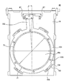
- FIG. 16 is a rear view of the regulation plate 60 having the opening 60a having the maximum inner diameter
- FIG. 17 is a rear view of the regulation plate 60 having the opening 60a having the minimum inner diameter.
- the lever portion 102 of the rotating member 100 is positioned relatively to the right and is movable by a stopper 67 provided on the plate body portion 61. The range is limited.
- the first blade 71 (not shown) is located at the outermost position in the radial direction of the opening 60 a, and the inner peripheral edge of the first blade 71 substantially coincides with the inner peripheral edge of the ring portion 101 of the rotating member 100. To do.
- the plate main body 61 is provided with four support pins 105.
- the support pin 105 is slidably engaged with a support long hole 103 provided in the convex portion 104 of the ring portion 101.
- the lever portion 102 of the rotating member 100 is positioned relatively to the left and is movable by a stopper 67 provided on the plate body portion 61.
- the range is limited.
- the plurality of first blades 71 are positioned at the innermost position in the radial direction of the opening 60 a, and the first blade 71 reduces the opening 60 a of the regulation plate 60.
- the lever unit 102 may be automatically operated by a mechanical actuator, for example, or may be manually operated by an operator.
- the lever portion 102 can also be fixed at an arbitrary position between the pair of stoppers 67.
- the diameter of the opening 60 a can be adjusted by narrowing the diameter of the opening 60 a with the plurality of first blades 71.
- the characteristics or processing conditions of the first substrate and the second substrate are different from each other, it is possible to suppress a decrease in in-plane uniformity due to the influence of the terminal effect.
- the substrate is plated under the condition where the influence of the terminal effect is conspicuous, by reducing the diameter of the opening a of the regulation plate 60, the film formation speed at the peripheral edge of the substrate is suppressed. And in-plane uniformity of the substrate can be improved.
- the plurality of first blades 71 can move in the radial direction while maintaining the angular relationship with the other first blades 71. Therefore, compared to the case where a plurality of aperture blades rotate about a predetermined axis to reduce the diameter of the opening as in the aperture mechanism of a camera, the circular shape of the inner peripheral edge formed by the first blade 71 is maintained. be able to.
- the first blade 71 has the slide pin 72 and the ring member 80 has the slide long hole 81.
- the present invention is not limited to this, and the ring member 80 may have the slide pin 72 and the first blade 71 may have the slide long hole 81 corresponding thereto. Even in the case where the first blade 71 and the ring member 80 are configured in this way, the ring pin 80 rotates in the circumferential direction, whereby the slide pin 72 slides in the slide long hole 81, and the first blade 71. Can move in the radial direction.
- the first blade 71 has a guide pin 73 and the blade pressing member 90 has a guide long hole 91.
- the present invention is not limited to this, and the blade pressing member 90 may have the guide pin 73 and the first blade 71 may have the guide long hole 91 corresponding thereto. Even when the first blade 71 and the blade pressing member 90 are configured in this way, when the first blade 71 is moved by the ring member 80, the guide pin 73 slides in the guide long hole 91, and the first blade 71 and the blade pressing member 90 are moved. The circumferential movement and rotation of the blade 71 can be prevented.
- a convex portion 104 having a support elongated hole 103 is formed in the ring portion 101 of the rotating member 100, and the support pin 105 is fixed to the plate main body portion 61.
- the present invention is not limited thereto, and the ring portion 101 of the rotating member 100 may have the support pins 105, and the plate main body portion 61 may have the corresponding support long holes 103. Even when the rotating member 100 and the plate main body 61 are configured in this way, when the ring portion 101 is swung by the lever portion 102, the support pin 105 slides in the support elongated hole 103, and the ring portion 101 can be rotated in its circumferential direction.
- the regulation plate 60 has only the blade body 70 (the plurality of first blades 71) as means for reducing the diameter of the opening 60a.
- the regulation plate 60 may include a plurality of second blades different from the plurality of first blades 71 and a mechanism that translates the plurality of second blades.
- the plurality of second blades are arranged at positions shifted from the plurality of first blades 71 in a direction orthogonal to the radial direction of the opening 60a.
- the mechanism that translates the plurality of second blades is the same as the above-described mechanism that translates the plurality of first blades 71, whereby the plurality of second blades translate in the radial direction of the opening 60a. Specific examples will be described below with reference to the drawings.
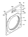
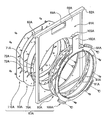
- FIG. 18 is a front perspective view of a regulation plate having a plurality of first blades and a plurality of second blades according to another embodiment
- FIG. 19 is a rear perspective view of the regulation plate.
- Components corresponding to those shown in FIGS. 4 to 17 in the drawings to be described below are given the same reference numerals used in FIGS. 4 to 17 with “A” or “B” added, and redundant descriptions are given. Is omitted.
- the regulation plate 60 of the present embodiment includes a first plate body 61A and a second plate body 61B.
- the first plate main body portion 61A has a first opening adjustment portion 63A
- the second plate main body portion 61B has a second opening adjustment portion 63B.
- the first plate body 61A and the second plate body 61B are connected to each other by an arbitrary fixing means 120 such as a screw or a bolt.
- the first plate body 61A and the second plate body 62B are brought into close contact with each other so as not to have a gap, and are connected to each other by the fixing means 120.
- the present invention is not limited to this, and the first plate body 61A and the second plate body 62B may be connected to each other with a gap. Further, the fixing means 120 may have an adjustment mechanism that adjusts the size of the gap between the first plate body 61A and the second plate body 62B. Thereby, the mutual distance of the some 1st braid
- the first plate main body 61A has an opening 69A for exposing the handle 105A of the rotating member 100A to the outside.
- the second plate body 61B has an opening 69B for exposing the handle 105B of the rotating member 100B to the outside.
- the handle portion 105A exposed from the opening 69A and the handle portion 105B exposed from the opening 69B can be independently operated using any actuator or manually. Accordingly, the plurality of first blades 71A and the plurality of second blades 71B shown in FIG. 21 can be independently translated in the radial direction.
- FIG. 20 is an exploded perspective view of the first plate body 61A and the second plate body 62B. As illustrated, the first plate body 61A and the second plate body 62B are connected to each other such that the surface on which the rotating member 100A is provided faces the surface on which the rotating member 100B is provided.
- the first plate body 61A has a cavity 68A that can accommodate the rotating member 100A and the rotating member 100B.
- the cavity 68A is configured to accommodate the rotating member 100A and the rotating member 100B when the first plate body 61A and the second plate body 61B are connected.
- the first plate main body 61A has a first opening 169A through which a current passes at a substantially central portion thereof.
- the second plate main body 61B has a second opening 169B through which a current passes at a substantially central portion thereof.
- the first plate body 61A and the second plate body 61B are connected to each other such that the center of the first opening 169A and the center of the second opening 169B are concentric.
- the first plate body 61A and the second plate body 61B are connected to each other so that the straight line connecting the center of the first opening 169A and the center of the second opening 169B is orthogonal to the radial direction of each opening. Is done.
- FIG. 21 is an exploded perspective view of the first plate body 61A.
- the first plate body 61A includes a blade body 70A, a ring member 80A, a blade pressing member 90A, a rotating member 100A, and a protection member 110A.
- the plurality of first blades 71A constituting the blade body 70 have two slide pins 72A.
- the ring member 80A has a pair of slide long holes 81A, two corresponding to the two slide pins 72A.
- FIG. 22 is an exploded perspective view of the second plate body 61B.
- the second plate body 61B includes a blade body 70B, a ring member 80B, a blade pressing member 90B, a rotating member 100B, and a protective member 110B.
- the plurality of second blades 71B constituting the blade body 70 have two slide pins 72B.
- the ring member 80B has a pair of slide long holes 81B, two corresponding to the two slide pins 72B.
- the first plate main body portion 61A and the second plate main body portion 61B are the centers of the openings formed by the plurality of first blades 71A shown in FIG. 21 and the openings formed by the plurality of second blades 71B shown in FIG. Are connected to each other so that their centers are concentric.
- the straight line connecting the centers of the openings formed by the plurality of first blades 71A and the centers of the openings formed by the plurality of second blades 71B is orthogonal to the radial direction of the respective openings.
- the plate body 61A and the second plate body 61B are connected to each other.
- the diameter of the opening 60a is reduced in both the plurality of first blades 71A and the plurality of second blades 71B. Can be squeezed.
- the film formation speed at the peripheral edge of the substrate can be further suppressed by the plurality of first blades 71A and the plurality of second blades 71B. Therefore, the in-plane uniformity of the substrate having a tendency to increase the film thickness at the peripheral edge of the substrate can be improved.
- the blade body 70A of the regulation plate 60 is composed of a plurality of first blades 71A
- the shape of the opening is not strictly a perfect circle. For this reason, it is difficult to completely remove the variation in the electric field applied to the substrate W due to the shape of the opening.
- the variation in the electric field due to the opening shape of the plurality of first blades 71A and the variation in the electric field due to the opening shape of the plurality of second blades 71B cancel each other.
- the variation in the electric field can be alleviated, and the plating film formed on the substrate W can be brought close to a perfect circle.
- the plurality of first blades 71 in the regulation plate 60 have an overlapping portion 75 with the adjacent first blade 71 and a portion that does not overlap with the adjacent first blade 71. Since the overlapping portion 75 is thicker than the non-overlapping portion, the electric field suppressing effect is different between the overlapping portion 75 and the non-overlapping portion. Therefore, the electric field may vary in the circumferential direction of the opening.
- the regulation plate 60 includes a plurality of second blades 71B in addition to the plurality of first blades 71A, the circumferential position of the overlapping portion of the plurality of second blades 71B is set to the overlap of the plurality of first blades 71A.
- the variation in the electric field due to the overlapping part of both blades can be reduced.
- the variation in electric field can be further alleviated by staggering the circumferential positions of the overlapping portions of the plurality of second blades 71B and the circumferential positions of the overlapping portions of the plurality of first blades 71A.
- the diameter of the opening 60A defined by the plurality of first blades 71A and the opening 60B defined by the plurality of second blades 71B can be made different. As a result, for example, the diameter of the opening defined by the blade close to the substrate is reduced, and the diameter of the opening defined by the blade far from the substrate is increased. Can be small.
- the in-plane uniformity of the plating film of the substrate W is adjusted by adjusting at least the diameter of the opening 25a of the anode mask 25 according to the characteristics of the substrate W or the conditions for processing the substrate W. Can be suppressed.
- the second substrate has a resist opening ratio.
- the change in the electrical resistance value from the center of the substrate to the electrical contact is small.
- the influence of the terminal effect on the second substrate remains large. Therefore, when the first substrate and the second substrate are plated under the same conditions other than the resist opening ratio of the substrate, the thickness of the peripheral portion of the second substrate is thicker than that of the first substrate. The film thickness at the center is relatively thin.
- the diameter of the opening 25 a of the anode mask 25 is made smaller than the diameter of the opening 25 a when plating the first substrate. Therefore, the film thickness of the center part of the second substrate can be increased. Therefore, it is possible to suppress a reduction in in-plane uniformity due to the influence of the terminal effect in both the first substrate and the second substrate.
- the terminal effect on the second substrate becomes remarkable.
- the thickness of the peripheral portion of the second substrate is larger than that of the first substrate,
- the film thickness at the center of the substrate is relatively thin. Therefore, when the second substrate is plated by the plating apparatus 10, the diameter of the opening 25 a of the anode mask 25 is made smaller than the diameter of the opening 25 a when plating the first substrate. Thereby, the film thickness of the center part of the second substrate can be increased. Therefore, it is possible to suppress a reduction in in-plane uniformity due to the influence of the terminal effect in both the first substrate and the second substrate.
- the second substrate is plated using a plating solution having a lower electrical resistance value than the plating solution used for the first substrate, as described above, the terminal effect on the second substrate is remarkable. Become. For this reason, when the first substrate and the second substrate are plated under the same conditions other than the electric resistance value of the plating solution, the thickness of the peripheral portion of the second substrate is thicker than that of the first substrate. The film thickness at the center of the substrate becomes relatively thin. Therefore, when the second substrate is plated by the plating apparatus 10, the diameter of the opening 25 a of the anode mask 25 is made smaller than the diameter of the opening 25 a when plating the first substrate. Thereby, the film thickness of the center part of the second substrate can be increased. Therefore, it is possible to suppress a reduction in in-plane uniformity due to the influence of the terminal effect in both the first substrate and the second substrate.
- the diameter of the opening 60a of the regulation plate 60 is adjusted, so that the in-plane of the plating film of the substrate W is adjusted. Uniformity can be improved.
- the regulation plate 60 is provided at a position closer to the substrate W than the anode mask 25. For this reason, the plating current that has passed through the opening 60 a of the regulation plate 60 is difficult to diffuse to the peripheral edge of the substrate W. Therefore, if the diameter of the opening 60a of the regulation plate 60 is reduced, the film thickness of the peripheral part of the substrate W can be reduced, and if the diameter of the opening 60a is increased, the film thickness of the peripheral part of the substrate W can be increased.
- the diameter of the opening 60 a of the regulation plate 60 is preferably adjusted as appropriate according to the film thickness distribution of the substrate W that changes by adjusting the diameter of the opening 25 a of the anode mask 25. Therefore, when plating on a second substrate having different characteristics of the first substrate or different conditions for processing the first substrate, the diameter of the opening 25a of the anode mask 25 is smaller than the diameter when processing the first substrate. Alternatively, the diameter is adjusted so as to increase, and the diameter of the opening 60a of the regulation plate 60 is appropriately changed.
- the regulation plate 60 has a plurality of first blades 71A and a plurality of second blades 71B as shown in FIGS. 18 to 22, openings 69A and 69B formed by the respective blades are independently formed. It can be changed as appropriate. Therefore, when plating on a plurality of substrates having different characteristics and processing conditions, it is possible to obtain an apparatus configuration capable of controlling the reduction of in-plane uniformity due to the influence of the terminal effect with higher accuracy.
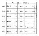
- FIG. 23 is a diagram showing the profile of the plating film of the substrate W having a high resist opening ratio (80%) and the substrate W having a low resist opening ratio (10%).
- “AM” is the diameter of the opening 25a of the anode mask 25
- “RP” is the diameter of the opening 60a of the regulation plate 60
- “HDP” is the substrate W having a high resist opening ratio
- “LDP” is the low resist opening ratio.
- the substrate W is shown.
- the substrate W with a high resist aperture ratio and the substrate W with a low resist aperture ratio both have a seed layer thickness of 50 nm to 100 nm, and the profile in FIG. 23 is plated using a relatively low resistance plating solution. This is the profile when
- condition A when the substrate W having a high resist aperture ratio is plated with the diameter of the opening 25a being 230 mm and the diameter of the opening 60a being 276 mm (hereinafter referred to as condition A), the film thickness at the center of the substrate is thick. The film thickness at the peripheral edge is reduced.
- condition C when the substrate W having a high resist opening ratio is plated with the diameter of the opening 25a being 270 mm and the diameter of the opening 60a being 276 mm (hereinafter referred to as condition C), the condition C is that the diameter of the opening 25a is the condition A. Therefore, the thickness of the central portion of the substrate is reduced.
- condition B when the substrate W having a high resist opening ratio is plated with the diameter of the opening 25a being 270 mm and the diameter of the opening 60a being 280 mm (hereinafter referred to as condition B), the condition B is smaller than the condition C in the diameter of the opening 60a. Since it is large, the film thickness at the peripheral edge of the substrate becomes thick.
- condition E When the substrate W having a low resist opening ratio is plated with the diameter of the opening 25a being 270 mm and the diameter of the opening 60a being 276 mm (hereinafter referred to as condition E), the film thickness at the center of the substrate is thin and the film thickness at the peripheral edge of the substrate. Becomes thicker. This means that the film thickness at the peripheral edge of the substrate is increased due to the influence of the terminal effect.
- condition F when the substrate W having a low resist opening ratio is plated with the diameter of the opening 25a being 220 mm and the diameter of the opening 60a being 276 mm (hereinafter referred to as condition F), the condition F is that the diameter of the opening 25a is the condition E. Therefore, the thickness of the central portion of the substrate becomes thicker.
- condition D when the substrate W having a low resist opening ratio is plated with the diameter of the opening 25a being 220 mm and the diameter of the opening 60a being 274 mm (hereinafter referred to as condition D), the condition D is smaller than the condition F in the diameter of the opening 60a. Since it is small, the film thickness at the peripheral edge of the substrate becomes thin.
- the diameter of the opening 25a is set to an opening 25a suitable for the plating process of the substrate W having a high resist opening ratio.
- the diameter of the opening 60a of the regulation plate 60 By adjusting the diameter of the opening 60a of the regulation plate 60, the film thickness of the peripheral portion of the substrate W can be adjusted, and the reduction in the in-plane uniformity of the film thickness of the substrate W due to the terminal effect is further suppressed. (See Condition D).
- FIG. 24 is a diagram showing the profile of the plating film of the substrate W having a thick seed layer (500 nm or more) and the substrate W having a thin seed layer (50 to 100 nm). Note that both the substrate W having a thick seed layer and the substrate W having a thin seed layer have a resist opening ratio of 10%, and the profile of FIG. 24 is obtained when plating is performed using a relatively low resistance plating solution. It is a profile.
- condition A when the substrate W having a thick seed layer is plated with the diameter of the opening 25a being 230 mm and the diameter of the opening 60a being 276 mm (hereinafter referred to as condition A), the film thickness at the center of the substrate is thick. The film thickness at the peripheral edge is reduced.
- condition C when the substrate W having a thick seed layer is plated with the diameter of the opening 25a being 270 mm and the diameter of the opening 60a being 276 mm (hereinafter referred to as condition C), the condition C is that the diameter of the opening 25a is the condition A. Therefore, the thickness of the central portion of the substrate is reduced.
- condition B when the substrate W having a thick seed layer is plated with the diameter of the opening 25a being 270 mm and the diameter of the opening 60a being 278 mm (hereinafter referred to as condition B), the condition B is smaller than the condition C in the diameter of the opening 60a. Since it is large, the film thickness at the peripheral edge of the substrate becomes thick.
- condition E When the substrate W having a thin seed layer is plated with the diameter of the opening 25a being 270 mm and the diameter of the opening 60a being 276 mm (hereinafter referred to as condition E), the film thickness at the center of the substrate is thin and the film thickness at the peripheral edge of the substrate. Becomes thicker. This means that the film thickness at the peripheral edge of the substrate is increased due to the influence of the terminal effect.
- condition F when the substrate W having a thin seed layer is plated with the diameter of the opening 25a being 220 mm and the diameter of the opening 60a being 276 mm (hereinafter referred to as condition F), the condition F is that the diameter of the opening 25a is equal to the condition E. Therefore, the thickness of the central portion of the substrate becomes thicker.
- condition D when the substrate W having a thin seed layer is plated with the diameter of the opening 25a being 220 mm and the diameter of the opening 60a being 274 mm (hereinafter referred to as condition D), the condition D is smaller than the condition F in the diameter of the opening 60a. Since it is small, the film thickness at the peripheral edge of the substrate becomes thin.
- the diameter of the opening 25a is set to an opening 25a suitable for the plating process of the substrate W having a thick seed layer.
- the diameter of the opening 60a of the regulation plate 60 By adjusting the diameter of the opening 60a of the regulation plate 60, the film thickness of the peripheral portion of the substrate W can be adjusted, and the reduction in the in-plane uniformity of the film thickness of the substrate W due to the terminal effect is further suppressed. (See Condition D).
- FIG. 25 shows the profile of the plating film of the substrate W plated with a plating solution having a relatively high electrical resistance (type-A) and the substrate W plated with a plating solution having a relatively low electrical resistance (type-B).
- condition A when the substrate W to be plated with a plating solution having a relatively high electrical resistance is plated with the diameter of the opening 25a being 230 mm and the diameter of the opening 60a being 276 mm (hereinafter referred to as condition A), The film thickness of the part is thick, and the film thickness of the peripheral part of the substrate is thin.
- condition C when the substrate W to be plated with a plating solution having a relatively high electrical resistance is plated with the diameter of the opening 25a being 260 mm and the diameter of the opening 60a being 276 mm (hereinafter referred to as condition C), the condition C Since the diameter of the opening 25a is larger than that of the condition A, the film thickness at the central portion of the substrate is reduced.
- condition B When the substrate W to be plated with a plating solution having a relatively high electrical resistance is plated with the diameter of the opening 25a being 260 mm and the diameter of the opening 60a being 272 mm (hereinafter referred to as condition B), the condition B is the opening 60a. Is smaller than the condition C, the film thickness at the peripheral edge of the substrate is reduced.
- the film thickness at the center of the substrate is It is thin, and the film thickness at the peripheral edge of the substrate is increased. This means that the film thickness at the peripheral edge of the substrate is increased due to the influence of the terminal effect.
- condition F when the substrate W to be plated with a plating solution having a relatively low electric resistance is plated with the diameter of the opening 25a being 220 mm and the diameter of the opening 60a being 276 mm (hereinafter referred to as condition F), the condition F Since the diameter of the opening 25a is smaller than that of the condition E, the film thickness at the central portion of the substrate is increased.
- condition D When the substrate W to be plated with a plating solution having a relatively low electrical resistance is plated with the diameter of the opening 25a being 220 mm and the diameter of the opening 60a being 274 mm (hereinafter referred to as condition D), the condition D is the opening 60a. Is smaller than the condition F, the film thickness at the peripheral edge of the substrate is reduced.
- the diameter of the opening 25a is set to a plating process for the substrate W plated with a plating solution having a relatively high electrical resistance.
- the change width of the diameter of the opening 25a of the anode mask 25 is the opening 60a of the regulation plate 60. It is desirable to make it larger than the change width of the diameter.
- a mechanism using the diaphragm blade 27 as described above is suitable.
- the anode mask 25 and the substrate W are separated from each other, even if the opening 25a of the anode mask 25 is reduced, the electric flux spreads between the anode mask 25 and the substrate W, and the film thickness of the plating film over a large range of the substrate W The distribution can be adjusted.
- the electric flux that spreads outside between the anode mask 25 and the substrate W is concentrated on the peripheral portion of the substrate W, so that the plating film tends to be thick.
- Such adjustment of the plating film thickness in a relatively narrow region of the peripheral edge of the substrate W is achieved by the opening adjusting portion 63 of the regulation plate 60. Since the regulation plate 60 is close to the substrate W, the electric field at the peripheral portion of the substrate W can be directly shielded, and the plating film thickness at the peripheral portion of the substrate W can be adjusted even with a relatively small change in opening diameter. .
- the plurality of diaphragm blades 27 are used as a mechanism for adjusting the diameter of the opening 25a of the anode mask 25, and the plurality of first blades 71A and the mechanism for adjusting the diameter of the opening 60a of the regulation plate 60 are used.
- a plurality of second blades 71B are used.
- the diameter of the opening 25a of the anode mask 25 may be adjusted by using the plurality of first blades 71A and the plurality of second blades 71B, and the opening 60a of the regulation plate 60 is adjusted by the plurality of diaphragm blades 27. You may do it.
Landscapes
- Chemical & Material Sciences (AREA)
- Engineering & Computer Science (AREA)
- Chemical Kinetics & Catalysis (AREA)
- Electrochemistry (AREA)
- Materials Engineering (AREA)
- Metallurgy (AREA)
- Organic Chemistry (AREA)
- Life Sciences & Earth Sciences (AREA)
- Sustainable Development (AREA)
- Automation & Control Theory (AREA)
- Electroplating Methods And Accessories (AREA)
- Electrodes Of Semiconductors (AREA)
Abstract
特徴及び処理条件の異なる複数の基板に対して、ターミナルエフェクトの影響による面内均一性の低下を抑制し得るレギュレーションプレート及びこれを備えためっき装置を提供する。 本発明の一形態によれば、アノードとめっきされる基板との間の電流を調整するためのレギュレーションプレートが提供される。このレギュレーションプレートは、電流が通過する開口を有するプレート本体部と、前記開口の径を絞るための複数の第1ブレードと、前記複数の第1ブレードを前記開口の径方向に並進移動させる第1移動機構と、を有する。
Description
本発明は、レギュレーションプレート、これを備えためっき装置及びめっき方法に関する。
従来、半導体ウェハ等の基板の表面に設けられた微細な配線用溝、ホール、又はレジスト開口部に配線を形成したり、基板の表面にパッケージの電極等と電気的に接続するバンプ(突起状電極)を形成したりすることが行われている。この配線及びバンプを形成する方法として、例えば、電解めっき法、蒸着法、印刷法、ボールバンプ法等が知られている。半導体チップのI/O数の増加、細ピッチ化に伴い、微細化が可能で性能が比較的安定している電解めっき法が多く用いられるようになってきている。
電解めっき法で配線又はバンプを形成する場合、基板上の配線用溝、ホール、又はレジスト開口部に設けられるバリアメタルの表面に電気抵抗の低いシード層(給電層)が形成される。このシード層の表面において、めっき膜が成長する。近年、配線及びバンプの微細化に伴って、より薄い膜厚のシード層が用いられている。シード層の膜厚が薄くなると、シード層の電気抵抗(シート抵抗)が増加する。
一般的に、めっきされる基板は、その周縁部に電気接点を有する。このため、基板の中央部には、めっき液の電気抵抗値と基板の中央部から電気接点までのシード層の電気抵抗値との合成抵抗に対応する電流が流れる。一方で、基板の周縁部(電気接点近傍)には、ほぼ、めっき液の電気抵抗値に対応する電流が流れる。即ち、基板の中央部には、基板の中央部から電気接点までのシード層の電気抵抗値の分だけ、電流が流れにくい。基板の周縁部に電流が集中するこの現象はターミナルエフェクトと呼ばれる。
比較的薄い膜厚のシード層を有する基板は、基板の中央部から電気接点までのシード層の電気抵抗値が比較的大きい。このため、比較的薄い膜厚のシード層を有する基板にめっきを行う場合、ターミナルエフェクトが顕著になる。その結果、基板の中央部におけるめっき速度が低下し、基板の中央部におけるめっき膜の膜厚が基板の周縁部におけるめっき膜よりも薄くなり、膜厚の面内均一性が低下する。
ターミナルエフェクトによる膜厚の面内均一性の低下を抑制するためには、基板に加わる電界を調節することが必要になる。たとえば、アノードと基板との間の電位分布を調整するための調整板をアノードと基板との間に設置しためっき装置が知られている(特許文献1参照)。
ところで、ターミナルエフェクトの影響は、基板のシード層の膜厚の大小によって異なる。具体的には、上述したように、シード層の膜厚が比較的薄い場合はシート抵抗が比較的大きいので、ターミナルエフェクトの影響が顕著に現れる。一方、シード層の膜厚が比較的厚い場合は、シート抵抗が比較的小さいので、ターミナルエフェクトの影響が比較的小さくなる。
また、ターミナルエフェクトの影響はシード層の膜厚の大小だけでなく、その他の要素によっても異なり得る。例えば、基板のレジスト開口率(レジスト外縁に縁取られる領域の面積のうち、レジストに覆われていない部分(レジストの開口部分)の面積の割合)が比較的高い場合は、基板上に形成されるめっき膜の面積が比較的大きい。このため、基板上にめっき膜が形成されるにつれて、形成されためっき膜によって基板中央部にも電流が流れやすくなる。言い換えれば、基板上にめっき膜が形成されるにつれて、基板の中央部から電気接点までの電気抵抗値が小さくなるので、ターミナルエフェクトの影響が徐々に小さくなる。一方で、基板のレジスト開口率が比較的低い場合は、基板上に形成されるめっき膜の面積が相対的に小さい。このため、基板のレジスト開口率が比較的低い場合は、基板上にめっき膜が形成されても、基板のレジスト開口率が比較的高い場合に比べて基板の中央部から電気接点までの電気抵抗値の変化が小さく、ターミナルエフェクトの影響が大きいままとなる。
また、基板を処理するめっき液の電気抵抗値が比較的大きい場合は、基板を処理するめっき液の電気抵抗値が比較的小さい場合に比べて、ターミナルエフェクトの影響が小さい。具体的には、めっき液の電気抵抗値をR1とし、基板の中央部から電気接点までのシード層の電気抵抗値をR2とした場合、基板中央部には、合成抵抗値(R1+R2)に対応する電流が流れる。一方で、基板周縁部(電気接点近傍)には、ほぼ、めっき液の電気抵抗値R1に対応する電流が流れる。したがって、電気抵抗値R1が大きくなれば、基板中央部に流れる電流に対する電気抵抗値R2の影響は小さくなり、ターミナルエフェクトの影響が小さくなる。
以上のように、ターミナルエフェクトの影響は、基板の特徴及び基板を処理する条件等によって異なる。このため、単一のめっき装置においてターミナルエフェクトの影響が異なる複数の基板に順次めっきをする場合、ターミナルエフェクトによる膜厚の面内均一性の低下を抑制するためには、それぞれの基板の特徴及び基板を処理する条件等に合わせて基板に加わる電界を調節する必要がある。しかしながら、特許文献1に記載されるような調整板で基板の特徴及び基板を処理する条件等に合わせて電界を調節するためには、基板の特徴及び基板を処理する条件等に合った調整板を複数用意しなくてはならない。
また、調整板を複数用意したとしても、特徴及び処理条件の異なる基板を処理するたびに、調整板をめっき槽から取り出し、別の調整板を設置する等の手間がかかる。
本発明は上記課題に鑑みてなされたものであり、その目的の一つは、特徴及び処理条件の異なる複数の基板に対してめっきするにあたり、ターミナルエフェクトの影響による面内均一性の低下を抑制し得るレギュレーションプレート、これを備えためっき装置及びめっき方法を提供することである。
第1形態によれば、アノードとめっきされる基板との間の電流を調整するためのレギュレーションプレートが提供される。このレギュレーションプレートは、電流が通過する第1の開口を形成する縁部を有するプレート本体部と、前記第1の開口の径を絞るための複数の第1ブレードと、前記複数の第1ブレードを前記第1の開口の径方向に並進移動させる第1移動機構と、を有する。
第1形態によれば、レギュレーションプレートの開口の径を第1ブレードにより絞ることで、開口の径を調節することができる。これにより、第1の基板と第2の基板の特徴又は処理条件が互いに異なる場合に、ターミナルエフェクトの影響による面内均一性の低下を抑制し得る。具体的には、ターミナルエフェクトの影響が顕著に現れる条件下で基板にめっきをする際には、レギュレーションプレートの開口の径を小さくすることにより、基板周縁部における成膜速度を抑制することができ、基板の面内均一性を向上させることができる。また、第1ブレードは並進移動するように構成されるので、他の第1ブレードとの角度関係を維持したまま、複数の第1ブレードが径方向に移動することができる。したがって、カメラの絞り機構のように複数の絞り羽根が所定の軸を中心に回転して開口の径を小さくする場合に比べて、第1ブレードによって形成される開口の真円形状を保つことができる。
第2形態によれば、第1形態において、前記第1移動機構は、前記縁部に沿うように配置されるリング部材を含み、前記リング部材及び前記複数の第1ブレードのいずれか一方は、前記第1の開口の径方向に対して傾斜したスライド長穴を有し、前記リング部材及び前記複数の第1ブレードの他方は、前記スライド長穴を摺動するスライドピンを有する。
第2形態によれば、リング部材及び複数の第1ブレードのいずれか一方に設けられたスライド長穴を、リング部材及び複数の第1ブレードの他方に設けられたスライドピンが摺動する。したがって、リング部材を周方向に回転させることで、スライドピンがスライド長穴を摺動し、第1ブレードを開口の径方向に移動させることができる。
第3形態によれば、第2形態において、前記第1移動機構は、前記複数の第1ブレードの前記リング部材とは逆側に固定されるブレード押さえ部材を含み、前記ブレード押さえ部材及び前記複数の第1ブレードのいずれか一方は、前記第1ブレードの並進移動方向と平行に形成されるガイド長穴を有し、前記ブレード押さえ部材及び前記複数の第1ブレードの他方は、前記ガイド長穴を摺動するガイドピンを有する。
第2形態によれば、ブレード押さえ部材及び複数の第1ブレードのいずれか一方に設けられたガイド長穴を、ブレード押さえ部材及び複数の第1ブレードの他方に設けられたガイドピンが摺動する。したがって、移動機構によって複数の第1ブレードが移動されたときに、複数の第1ブレードが回転運動することを防止しつつ、第1ブレードを所望の方向に並進移動させることができる。
第4形態によれば、第2又は第3形態において、前記第1移動機構は、前記リング部材を周方向に回転させるための回転部材を含み、前記回転部材は、前記リング部材に固定されるリング部と、前記リング部を周方向に回転させるレバー部と、を有する。
第4形態によれば、レバー部をアクチュエータや手動で操作することにより、リング部を周方向に回転させることができる。リング部はリング部材に固定されているので、リング部の回転に伴ってリング部材が回転する。これにより、リング部材に設けられたスライド長穴又はスライドピンが、複数の第1ブレードに設けられたスライドピン又はスライド長穴と摺動し、複数の第1ブレードを並進移動させることができる。
第5形態によれば、第4形態において、前記プレート本体部及び前記リング部のいずれか一方は、前記リング部の回転方向に沿って形成された支持長穴を有し、前記プレート本体部及び前記リング部の他方は、前記支持長穴と摺動可能に係合する支持ピンを有する。
第5形態によれば、プレート本体部及びリング部のいずれか一方に設けられた支持長穴に対して、プレート本体部及びリング部の他方に設けられた支持ピンが摺動可能に係合する。支持ピンが支持長穴と係合することにより、リング部がプレート本体部に支持される。支持長穴はリング部の回転方向に沿って形成されるので、支持ピンが支持長穴を摺動することで、リング部を回転させることができる。
第6形態によれば、第1から第5形態のいずれかにおいて、前記複数の第1ブレードの各々は、その内周縁が円弧状に形成され、他の前記第1ブレードと互いに重なり合って略円形の内周縁を形成する。
第6形態によれば、複数の第1ブレードが開口の径方向に並進移動して開口の径を縮小させたとき、複数の第1ブレードの内周縁が略円形を保つことができる。
第7形態によれば、第1から第6形態のいずれかにおいて、レギュレーションプレートは、前記第1の開口の径方向と直交する方向に前記複数の第1ブレードからずれた位置に配置され、前記第1の開口の径を絞るための複数の第2ブレードと、前記複数の第2ブレードを前記第1の開口の径方向に並進移動させる第2移動機構と、を有する。
第7形態によれば、レギュレーションプレートは、複数の第1ブレードによって形成される第1の径を有する開口と、複数の第2ブレードによって形成される第2の径を有する開口とを有する。第1の径と第2の径との大きさをそれぞれ適切に調節することにより、レギュレーションプレートの開口を通過する電流をより適切に調整することができる。
第8形態によれば、第7形態において、前記複数の第1ブレードにより形成される開口の中心と前記複数の第2ブレードにより形成される開口の中心とを結ぶ直線がこれらの開口の径方向と直交するように、前記第1ブレード及び前記第2ブレードが配置される。
第8形態によれば、第1ブレードにより形成される開口中心と第2ブレードにより形成される開口中心が互いに一致するように、第1ブレード及び第2ブレードが配置される。したがって、レギュレーションプレートをめっき槽に位置決めする際に、複数の第1ブレードにより形成される開口中心と、複数の第2ブレードにより形成される開口中心とを、それぞれ別々に位置決めする必要がない。このため、レギュレーションプレートの開口中心の位置に高い精度が求められる場合であっても、レギュレーションプレートを容易に位置決めすることができる。
第9形態によれば、アノードとめっきされる基板との間の電流を調整するためのレギュレーションプレートが提供される。このレギュレーションプレートは、電流が通過する第1の開口を形成する第1縁部と、前記第1の開口の径を絞るための複数の第1ブレードと、を有する第1プレート本体部と、電流が通過する第2の開口を形成する第2縁部と、前記第2の開口の径を絞るための複数の第2ブレードと、を有する第2プレート本体部と、を有する。前記複数の第1ブレードにより形成される開口の中心と前記複数の第2ブレードにより形成される開口の中心とを結ぶ直線がこれら開口の径方向と直交するように、前記第1プレート本体部と第2プレート本体部とが互いに連結される。
第9形態によれば、レギュレーションプレートは、複数の第1ブレードによって形成される第1の径を有する開口と、複数の第2ブレードによって形成される第2の径を有する開口とを有する。第1の径と第2の径との大きさをそれぞれ適切に調節することにより、レギュレーションプレートの開口を通過する電流をより適切に調整することができる。また、第1ブレードにより形成される開口中心と第2ブレードにより形成される開口中心が互いに一致するように、第1ブレード及び第2ブレードが配置される。したがって、レギュレーションプレートをめっき槽に位置決めする際に、複数の第1ブレードにより形成される開口中心と、複数の第2ブレードにより形成される開口中心とを、それぞれ別々に位置決めする必要がない。このため、レギュレーションプレートの開口中心の位置に高い精度が求められる場合であっても、レギュレーションプレートを容易に位置決めすることができる。
第10形態によれば、第7から第9形態のいずれかにおいて、前記複数の第1ブレードにより形成される開口の径と、前記複数の第2ブレードにより形成される開口の径とを互いに独立して調整することができるように構成される。
第10形態によれば、複数の第1ブレードが画定する開口の径と、複数の第2ブレードが画定する開口の径とを異ならせることができる。これにより、例えば、基板に近いブレードが画定する開口の径を小さくし、基板に遠いブレードが画定する開口の径を大きくする等、基板の特徴や処理条件に合わせて開口の径を段階的に小さくすることができる。
第11形態によれば、めっき装置が提供される。このめっき装置は、アノードを保持するように構成されたアノードホルダと、前記アノードホルダと対向して配置され、基板を保持するように構成された基板ホルダと、前記アノードホルダに一体に取り付けられ、前記アノードと前記基板との間に流れる電流が通過する第2の開口を有するアノードマスクと、上記いずれかのレギュレーションプレートと、を有し、前記アノードマスクは、前記第2の開口の径を調節する調節機構を有する。
第11形態によれば、第1の基板と第2の基板のそれぞれに対して、アノードマスクの第2の開口の径を調節することができる。これにより、第1の基板と第2の基板の特徴又は処理条件が互いに異なる場合に、ターミナルエフェクトの影響による面内均一性の低下を抑制し得る。具体的には、ターミナルエフェクトの影響が顕著に現れる条件下で第2の基板にめっきをする際には、第2の開口の径を小さくすることにより、基板中央部に電界を集中して、基板中央部の膜厚を厚くすることができる。また、レギュレーションプレートの第1の開口の径を小さくすると、基板周縁部における成膜速度を抑制することができる。したがって、レギュレーションプレートの第1の開口の径と、アノードマスクの第2の開口の径との両方を調節することで、基板Wの面内均一性をいっそう向上させることができる。
第12形態によれば、めっき方法が提供される。このめっき方法は、アノードと基板との間に流れる電流が通過する第1の開口を有するアノードマスクを一体に備えるアノードホルダをめっき槽内に配置する工程と、第1の基板を保持する基板ホルダをめっき槽内に配置する工程と、前記アノードと前記基板との間に流れる電流が通過する第2の開口及び第3の開口を有するレギュレーションプレートを前記アノードマスクと前記基板との間に配置する工程と、前記第1の開口の径を第1の径に調節して、第1の基板にめっきする工程と、第2の基板を保持する基板ホルダをめっき槽内に配置する工程と、前記第1の開口の径を前記第1の径よりも小さい第2の径に調節するとともに、前記レギュレーションプレートの第2の開口及び第3の開口の径をそれぞれ変更して、前記第2の基板をめっきする工程と、を有する。
第12形態によれば、第1の基板と第2の基板のそれぞれに対して、アノードマスクの第1の開口の径を調節することができる。これにより、第1の基板と第2の基板の特徴又は処理条件が互いに異なる場合に、ターミナルエフェクトの影響による面内均一性の低下を抑制し得る。具体的には、ターミナルエフェクトの影響が顕著に現れる条件下で第2の基板にめっきをする際には、第1の開口の径を小さくすることにより、基板中央部に電界を集中して、基板中央部の膜厚を厚くすることができる。また、レギュレーションプレートの第2の開口の径及び第3の開口の径をそれぞれ変更することで、基板周縁部における成膜速度を抑制することができ、基板Wの面内均一性を向上させることができる。
以下、本発明の実施形態について図面を参照して説明する。以下で説明する図面において、同一の又は相当する構成要素には、同一の符号を付して重複した説明を省略する。
図1は、本実施形態に係るめっき装置の概略側断面図である。図示のように、本実施形態に係るめっき装置10は、アノード21を保持するように構成されたアノードホルダ20と、基板Wを保持するように構成された基板ホルダ40と、アノードホルダ20と基板ホルダ40とを内部に収容するめっき槽50と、を有する。
図1に示すように、めっき槽50は、添加剤を含むめっき液Qを収容するめっき処理槽52と、めっき処理槽52からオーバーフローしためっき液Qを受けて排出するめっき液排出槽54と、めっき処理槽52とめっき液排出槽54とを仕切る仕切り壁55と、を有する。
アノード21を保持したアノードホルダ20と基板Wを保持した基板ホルダ40は、めっき処理槽52内のめっき液Qに浸漬され、アノード21と基板Wの被めっき面W1が略平行になるように対向して設けられる。アノード21と基板Wは、めっき処理槽52のめっき液Qに浸漬された状態で、めっき電源59により電圧が印加される。これにより、金属イオンが基板Wの被めっき面W1において還元され、被めっき面W1に膜が形成される。
めっき処理槽52は、槽内部にめっき液Qを供給するためのめっき液供給口56を有する。めっき液排出槽54は、めっき処理槽52からオーバーフローしためっき液Qを排出するためのめっき液排出口57を有する。めっき液供給口56はめっき処理槽52の底部に配置され、めっき液排出口57はめっき液排出槽54の底部に配置される。
めっき液Qがめっき液供給口56からめっき処理槽52に供給されると、めっき液Qはめっき処理槽52から溢れ、仕切り壁55を越えてめっき液排出槽54に流入する。めっき液排出槽54に流入しためっき液Qはめっき液排出口57から排出され、めっき液循環装置58が有するフィルタ等で不純物が除去される。不純物が除去されためっき液Qは、めっき液循環装置58によりめっき液供給口56を介してめっき処理槽52に供給される。
アノードホルダ20は、アノード21と基板Wとの間の電界を調節するためのアノードマスク25を有する。アノードマスク25は、例えば誘電体材料からなる略板状の部材であり、アノードホルダ20の前面に設けられる。ここで、アノードホルダ20の前面とは、基板ホルダ40に対向する側の面をいう。すなわち、アノードマスク25は、アノード21と基板ホルダ40の間に配置される。アノードマスク25は、アノード21と基板Wとの間に流れる電流が通過する開口25a(第2の開口の一例に相当する)を略中央部に有する。開口25aの径は、アノード21の径よりも小さいことが好ましい。後述するように、アノードマスク25は、開口25aの径を調節可能に構成される。
アノードマスク25は、アノードマスク25をアノードホルダ20に一体に取り付けるためのアノードマスク取付け部25bを、その外周に有する。なお、アノードマスク25の位置は、アノードホルダ20と基板ホルダ40との間であればよいが、アノードホルダ20と基板ホルダ40との中間位置よりもアノードホルダ20に近い位置であることが好ましい。また、例えばアノードマスク25は、アノードホルダ20に取り付けられずにアノードホルダ20の前面に配置してもよい。ただし、本実施形態のようにアノードマスク25がアノードホルダ20に取り付けられる場合は、アノードホルダ20に対するアノードマスク25の相対位置が固定されるので、アノード21の位置と開口25aの位置とがずれることを防止することができる。
アノードホルダ20に保持されるアノード21は、不溶性アノードであることが好ましい。アノード21が不溶性アノードである場合は、めっき処理が進んでもアノード21は溶解せず、アノード21の形状が変化することがない。このため、アノードマスク25とアノード21の表面との位置関係(距離)が変化しないので、アノードマスク25とアノード21の表面との位置関係が変化することによりアノード21と基板Wとの間の電界が変化することを防止することができる。
めっき装置10は、さらに、アノード21と基板Wとの間の電流を調整するためのレギュレーションプレート60を有する。レギュレーションプレート60は、例えば誘電体材料からなる略板状の部材であり、アノードマスク25と基板ホルダ40(基板W)との間に配置される。レギュレーションプレート60は、アノード21と基板Wとの間に流れる電流が通過する開口60a(第1の開口の一例に相当する)を有する。開口60aの径は、基板Wの径より小さいことが好ましい。後述するように、レギュレーションプレート60は、開口60aの径を調節可能に構成される。
レギュレーションプレート60は、アノードホルダ20と基板ホルダ40との中間位置よりも基板ホルダ40に近い位置にあることが好ましい。レギュレーションプレート60が基板ホルダ40に近い位置に配置されるほど、レギュレーションプレート60の開口60aの径を調節することにより、基板Wの周縁部の膜厚をより正確に制御することができる。
レギュレーションプレート60と基板ホルダ40との間には、基板Wの被めっき面W1近傍のめっき液Qを撹拌するためのパドル18が設けられる。パドル18は、略棒状の部材であり、鉛直方向を向くようにめっき処理槽52内に設けられる。パドル18の一端は、パドル駆動装置19に固定される。パドル18は、パドル駆動装置19により基板Wの被めっき面W1に沿って水平移動され、これによりめっき液Qが撹拌される。
次に、図1に示したアノードマスク25について詳細に説明する。図2及び図3はアノードマスク25の概略正面図である。図2は、開口25aの径が比較的大きいときのアノードマスク25を示す。図3は、開口25aの径が比較的小さいときのアノードマスク25を示す。ここで、アノードマスク25の開口25aが小さいほど、アノード21から基板Wへ流れる電流が、基板Wの被めっき面W1の中央部に集中する。したがって、開口25aを小さくすると、基板Wの被めっき面W1の中央部の膜厚が増大する傾向がある。
図2に示すように、アノードマスク25は、略環状の縁部26を有する。図2に示すアノードマスク25の開口25aの径の大きさは最大となっている。この場合の開口25aの径は、縁部26の内径と一致する。
図3に示すように、アノードマスク25は、開口25aを調節可能に構成される複数の絞り羽根27(調節機構の一例に相当する)を有する。絞り羽根27は、協働して開口25aを画定する。絞り羽根27の各々は、カメラの絞り機構と同様の構造により、開口25aの径を拡大又は縮小させる(開口25aの径を調節する)。図3に示すアノードマスク25の開口25aは、絞り羽根27によって非円形状(例えば多角形状)に形成される。この場合の開口25aの径は、多角形の対向する辺の最短距離、又は内接する円の直径をいう。あるいは、開口25aの径は、開口面積と等価な面積を有する円の直径で定義することもできる。なお、アノード21と、絞り羽根27のアノード21と対向する面の距離は、例えば0mm以上8mm以下である。
絞り羽根27の各々は、例えば手動により開口25aの径を拡大又は縮小させる。また、絞り羽根27の各々は、エア圧力あるいは電気的な駆動力を利用して駆動するように構成されてもよい。絞り羽根27を用いた調節機構は、比較的広範囲に開口25aを可変とすることができる特徴がある。また、基板が円形である場合には、アノードマスク25の開口25aは円形であることが望ましい。しかし、比較的広範囲に径が可変である開口25aにおいて、開口25aの最小径から最大径に至る全ての範囲で完全な円形を維持することは機構的な困難を伴う。一般的に、アノード21と基板Wとの間を流れる電流が通過する開口が完全な円形でない場合、電場の方位角分布が不均等になり、基板Wの周縁部に形成されるめっき膜厚分布に開口の形状が転写される可能性がある。しかしながら、アノードマスク25はアノードホルダ20に一体的に取り付けられているため、基板との距離を十分に取ることができ、開口が完全な円形でない場合でも、めっき膜厚分布に与える影響を最大限に抑えることができる。
次に、図1に示したレギュレーションプレート60について詳細に説明する。図4は、開口60aの径が比較的大きい状態のレギュレーションプレート60の前面側斜視図を示し、図5は、開口60aの径が比較的大きい状態のレギュレーションプレート60の後面側斜視図を示す。また、図6は、開口60aの径が比較的小さい状態のレギュレーションプレート60の正面側斜視図を示す。
図4ないし図6に示すように、レギュレーションプレート60は、略板状のプレート本体部61を有する。プレート本体部61は、その上部の左右端部に、図1に示しためっき処理槽52の縁にレギュレーションプレート60を懸架して吊下げるための一対の吊下げ部62を有する。また、プレート本体部61は、その略中央部に開口60aを有する。開口60aは、プレート本体部61に設けられる開口調節部63によって形成される。
図5に示すように、レギュレーションプレート60の背面側には、開口調節部63の一部を構成する回転部材100が取り付けられる。また、図6に示すように、レギュレーションプレート60は、開口60aの径を絞るように構成されたブレード体70を有する。回転部材100及びブレード体70の詳細は後述する。
図7は、レギュレーションプレート60の分解斜視図である。図7に示すように、レギュレーションプレート60は、プレート本体部61と、ブレード体70と、リング部材80と、ブレード押さえ部材90と、回転部材100と、保護部材110と、を有する。ブレード体70、リング部材80、ブレード押さえ部材90、回転部材100、及び保護部材110により、開口調節部63が構成される。また、レギュレーションプレート60は、プレート本体部61とともに開口60aを形成する縁部64を有する。
ブレード体70は、開口60aの径を絞るための複数の第1ブレード71を有し、レギュレーションプレート60の縁部64の前面側に位置する。なお、本実施形態において、レギュレーションプレート60の前面側とは、図1に示した基板ホルダ40に対向する面をいう。しかしながら、他の実施形態では、レギュレーションプレート60の前面側が図1に示したアノードホルダ20に対向するように、レギュレーションプレート60を図1のめっき処理槽52に配置してもよい。
リング部材80は、複数の第1ブレード71を開口60aの径方向に並進移動させるように構成される。リング部材80は、レギュレーションプレート60の縁部64に沿って配置される。本実施形態では、リング部材80は、レギュレーションプレート60の縁部64の内周面に沿って配置される。しかし、これに限らず、リング部材80は、例えば、レギュレーションプレート60の縁部64の前面側に配置されてもよい。
ブレード押さえ部材90は、ブレード体70の前面側(リング部材80とは反対側)に配置される。回転部材100は、プレート本体部61の後面側に配置され、後述するようにリング部材80と結合される。以下、レギュレーションプレート60を構成する各部材について詳細に説明する。
図8は、プレート本体部61の前面側斜視図を示し、図9は、プレート本体部61の後面側斜視図を示す。図8に示すように、プレート本体部61は、略板状の部材であり、その略中央部に開口60aを有する。プレート本体部61の前面側には、開口60aと略同一の開口を有する縁部64が固定される。縁部64は、プレート本体部61と共に開口60aを形成している。図9に示すように、プレート本体部61は、後面側に、回転部材100を摺動可能に支持する支持ピンを挿入するための複数のピン穴65を有する。また、縁部64は、ブレード押さえ部材90と保護部材110とを固定するねじを螺合するための複数のねじ穴66をその前面側に有する。
図10は、リング部材80の前面側斜視図を示す図である。上述したように、リング部材80は、図8及び図9に示したプレート本体部61の開口60aの内周面に沿って配置される。したがって、リング部材80の外径は、プレート本体部61の開口60aを構成する縁部64の内径とおよそ一致するように構成される。このため、リング部材80の内径が、開口60aの最大内径となる。図示のように、リング部材80(第1移動機構の一例に相当する)は、その前面側に複数のスライド長穴81を有する。本実施形態では、ブレード体70を構成する第1ブレード71の数に対応する8つのスライド長穴81がリング部材80に設けられる。スライド長穴81は、リング部材80の後面側に向かって貫通していても、そうでなくてもよい。スライド長穴81は、開口60aの径方向に対して傾斜するように構成される。言い換えれば、スライド長穴81は、その長穴の長手方向が開口60aの中心を向かないように傾斜して配置される。スライド長穴81の各々は、互いに開口60aの中心軸に対して回転対称となるように、リング部材80に設けられる。本実施形態では、8つのスライド長穴81が設けられるので、スライド長穴81の各々は、8回回転対称となる。
図11は、回転部材100の前面側斜視図を示す。回転部材100は、リング部101と、リング部101に取り付けられる板状のレバー部102とを有する。リング部101は、図10に示したリング部材80の後面側に固定される。リング部101の内径は、リング部材80の内径と略一致するように構成される。レバー部102は、リング部101の外周部に結合され、レバー部102をリング部101の周方向に揺動させることにより、リング部101が揺動角度の範囲で周方向に回転する。
リング部101の外周には4つの凸部104が設けられ、凸部104の各々には、リング部101の周方向に沿った支持長穴103が形成される。後述するように、支持長穴103は、図9に示したプレート本体部61のピン穴65に固定される支持ピンにより、摺動可能に支持される。
図12は、ブレード体70を構成する第1ブレード71の前面側斜視図を示す。図示のように第1ブレード71は、その内周縁が円弧状に形成された扇形の部材である。第1ブレード71は、図7に示したように他の第1ブレード71と互いに重なり合って、全体としてブレード体70の略円形の内周縁を形成する。本実施形態では、8つの第1ブレード71によりブレード体70が構成されるが、これに限らず任意の数の第1ブレード71でブレード体70を構成することができる。
第1ブレード71の後面側には、図10に示したリング部材80のスライド長穴81内を摺動するように構成されるスライドピン72が設けられる。本実施形態では、1つのスライドピン72が第1ブレード71に設けられるが、これに限らず、2つ以上のスライドピン72を第1ブレード71に設けてもよい。この場合、図10に示したリング部材80のスライド長穴81の数をスライドピン72の数に合わせる必要がある。
また、第1ブレード71の前面側には、後述する図13に示すブレード押さえ部材90のガイド長穴91を摺動するように構
成されるガイドピン73が設けられる。本実施形態では、2つのガイドピン73が第1ブレード71に設けられるが、これに限らず、1つ又は3つ以上のガイドピン73が第1ブレード71に設けられてもよい。
成されるガイドピン73が設けられる。本実施形態では、2つのガイドピン73が第1ブレード71に設けられるが、これに限らず、1つ又は3つ以上のガイドピン73が第1ブレード71に設けられてもよい。
図13は、ブレード押さえ部材90の前面側斜視図である。ブレード押さえ部材90は、略板状の部材であり、その略中央部に開口60aが形成される。ブレード押さえ部材90の開口60aの径は、図10に示したリング部材80の内径と略同一の径を有する。ブレード押さえ部材90は、複数のガイド長穴91を有する。本実施形態では、16のガイド長穴91がブレード押さえ部材90に設けられ、図12に示した第1ブレード71の2つのガイドピン73のそれぞれに2つのガイド長穴91が対応する。ガイド長穴91の数は、ガイドピン73の数に応じて適宜変更可能である。ガイド長穴91は、第1ブレード71の並進移動方向と平行に形成される。また、ブレード押さえ部材90は複数のねじ穴92を有する。図8に示したプレート本体部61の縁部64に形成されたねじ穴66の位置とねじ穴92の位置を合わせて、ねじを螺合することで、ブレード押さえ部材90をプレート本体部61に固定することができる。
ブレード押さえ部材90は、その後面側がブレード体70の前面側と接触するように配置される。したがって、ブレード体70の第1ブレード71が開口60aの径方向に並進移動したとき、第1ブレード71はブレード押さえ部材90と接触しながら並進移動する。ブレード押さえ部材90と第1ブレード71との摩耗を低減するために、ブレード押さえ部材90は、例えばPTFE等の低摩擦の樹脂から構成されることが好ましい。
図14は、保護部材110の前面側斜視図である。保護部材110は、略板状の部材であり、その略中央部に開口60aが形成される。保護部材110の開口60aの径は、図10に示したリング部材80の内径と略同一の径を有する。保護部材110は、ブレード押さえ部材90の前面側に配置される。保護部材110は複数のねじ穴111を有する。図8に示したねじ穴66及び図13に示したねじ穴92の位置とねじ穴111の位置を合わせて、ねじを螺合することで、保護部材110をプレート本体部61に固定することができる。保護部材110は、例えば塩化ビニル等から構成され、ブレード押さえ部材90の前面側を保護する。
次に、図12に示した第1ブレード71を並進移動させる機構について詳細に説明する。図15は、レギュレーションプレート60の前面側からの部分正面図である。図15においては、回転部材100、複数の第1ブレード71、ブレード押さえ部材90、及びリング部材80のスライド長穴81が、それぞれ透過されて示されており、その他の部材は図示の簡略化のため省略されている。
図15に示すように、複数の第1ブレード71は、他の第1ブレード71と互いに一部が重なる重なり部75を有するように配置される。複数の第1ブレード71の内周縁は、略円形状に形成される。図示の状態では、複数の第1ブレード71のスライドピン72はスライド長穴81の略中間部に位置し、ガイドピン73はガイド長穴91の略中間部に位置している。図示の状態では、複数の第1ブレード71の内周縁の内径は、レギュレーションプレート60の開口60aの内径よりも小さい。したがって、複数の第1ブレード71は、レギュレーションプレート60の開口60aの内径を縮小させている。
回転部材100のレバー部102が矢印A1又はA2の方向、即ちリング部101の周方向に移動すると、リング部101と結合した図示しないリング部材80もその周方向に回転する。例えば、レバー部102が矢印A1の方向(図中時計回り)に移動すると、リング部材80が時計回りに回転する。これにより、第1ブレード71のスライドピン72はスライド長穴81内を摺動し、スライド長穴81の最小径部分81aがスライドピン72に向かって移動する。このとき、スライド長穴81の最小径部分81aがスライドピン72に向かって移動するのに伴い、第1ブレード71は、開口60aの径方向内側に向かって移動する。第1ブレード71のガイドピン73は、ガイド長穴91の内部を摺動するので、第1ブレード71の周方向の移動及び回転運動が防止される。したがって、第1ブレード71は、確実に径方向に並進移動することができる。
また、例えば、レバー部102が矢印A2の方向(図中反時計回り)に移動すると、リング部材80が反時計回りに回転する。これにより、第1ブレード71のスライドピン72はスライド長穴81内を摺動し、スライド長穴81の最大径部分81bがスライドピン72に向かって移動する。このとき、スライド長穴81の最大径部分81bがスライドピン72に向かって移動するのに伴い、第1ブレード71は、開口60aの径方向外側に向かって並進移動する。
複数の第1ブレード71は、それぞれ同様に径方向に並進移動する。したがって、第1ブレード71と他の第1ブレード71との角度関係を維持したまま、複数の第1ブレードが径方向に移動することができる。これにより、カメラの絞り機構のように複数の絞り羽根が所定の軸を中心に回転して開口の径を小さくする場合に比べて、第1ブレード71によって形成される内周縁の真円形状を保つことができる。
図16は、最大内径の開口60aを有するレギュレーションプレート60の後面図であり、図17は、最小内径の開口60aを有するレギュレーションプレート60の後面図である。図16に示すように、レギュレーションプレート60が最大内径の開口60aを有するときは、回転部材100のレバー部102は相対的に右方向に位置し、プレート本体部61に設けられるストッパ67によってその可動範囲が制限される。図16に示す状態では、図示しない第1ブレード71は、開口60aの径方向で最外位置に位置し、第1ブレード71の内周縁は、回転部材100のリング部101の内周縁と略一致する。
プレート本体部61には、4つの支持ピン105が設けられる。支持ピン105は、リング部101の凸部104に設けられる支持長穴103と摺動可能に係合する。これにより、レバー部102を操作したときに、リング部101が、支持長穴103に沿って周方向に回転するようにガイドされる。
図17に示すように、レギュレーションプレート60が最小内径の開口60aを有するときは、回転部材100のレバー部102は相対的に左方向に位置し、プレート本体部61に設けられるストッパ67によってその可動範囲が制限される。図17に示す状態では、複数の第1ブレード71は、開口60aの径方向で最内位置に位置し、第1ブレード71は、レギュレーションプレート60の開口60aを縮小させている。
レバー部102は、例えば機械的なアクチュエータによって自動的に操作されてもよいし、作業員により手動で操作されてもよい。また、レバー部102は、一対のストッパ67間の任意の位置で固定することもできる。
以上で説明したように、本実施形態に係るレギュレーションプレート60によれば、開口60aの径を複数の第1ブレード71により絞ることで、開口60aの径を調節することができる。これにより、第1の基板と第2の基板の特徴又は処理条件が互いに異なる場合に、ターミナルエフェクトの影響による面内均一性の低下を抑制し得る。具体的には、ターミナルエフェクトの影響が顕著に現れる条件下で基板にめっきをする際には、レギュレーションプレート60の開口aの径を小さくすることにより、基板周縁部における成膜速度を抑制することができ、基板の面内均一性を向上させることができる。また、第1ブレード71は並進移動するように構成されるので、他の第1ブレード71との角度関係を維持したまま、複数の第1ブレード71が径方向に移動することができる。したがって、カメラの絞り機構のように複数の絞り羽根が所定の軸を中心に回転して開口の径を小さくする場合に比べて、第1ブレード71によって形成される内周縁の真円形状を保つことができる。
なお、本実施形態では、第1ブレード71がスライドピン72を有し、リング部材80がスライド長穴81を有する。しかしながら、これに限らず、リング部材80がスライドピン72を有し、これに対応するスライド長穴81を第1ブレード71が有してもよい。このように第1ブレード71とリング部材80を構成した場合であっても、リング部材80が周方向に回転することで、スライドピン72がスライド長穴81内を摺動し、第1ブレード71が径方向に移動することができる。
本実施形態では、第1ブレード71がガイドピン73を有し、ブレード押さえ部材90がガイド長穴91を有する。しかしながら、これに限らず、ブレード押さえ部材90がガイドピン73を有し、これに対応するガイド長穴91を第1ブレード71が有してもよい。このように第1ブレード71とブレード押さえ部材90を構成した場合であっても、第1ブレード71がリング部材80によって移動したとき、ガイドピン73がガイド長穴91内を摺動し、第1ブレード71の周方向の移動及び回転運動を防止することができる。
本実施形態では、回転部材100のリング部101に支持長穴103を有する凸部104が形成され、プレート本体部61に支持ピン105が固定される。しかしながら、これに限らず、回転部材100のリング部101が支持ピン105を有し、これに対応する支持長穴103をプレート本体部61が有してもよい。このように回転部材100とプレート本体部61を構成した場合であっても、リング部101がレバー部102によって揺動されたとき、支持ピン105が支持長穴103内を摺動し、リング部101をその周方向に回転させることができる。
さらに、本実施形態では、レギュレーションプレート60は、開口60aの径を縮小する手段として、ブレード体70(複数の第1ブレード71)のみを有する。しかしながら、レギュレーションプレート60は、複数の第1ブレード71とは別の複数の第2ブレードと、複数の第2ブレードを並進移動させる機構を有してもよい。この場合、複数の第2ブレードは、開口60aの径方向と直交する方向に複数の第1ブレード71からずれた位置に配置される。この複数の第2ブレードを並進移動させる機構は、複数の第1ブレード71を並進移動させる上述した機構と同一であり、これにより、複数の第2ブレードが開口60aの径方向に並進移動する。以下、図面を参照して具体例を説明する。
図18は、他の実施形態に係る複数の第1ブレードと複数の第2ブレードとを有するレギュレーションプレートの前面側斜視図であり、図19は、同レギュレーションプレートの後面側斜視図である。以下で説明する図面における図4ないし17に示した部分に対応する構成要素には、図4ないし図17に使用した符号に「A」又は「B」を加えた符号を付し、重複した説明を省略する。
図18及び図19に示すように、本実施形態のレギュレーションプレート60は、第1プレート本体部61Aと第2プレート本体部61Bを有する。第1プレート本体部61Aは、第1開口調節部63Aを有し、第2プレート本体部61Bは第2開口調節部63Bを有する。第1プレート本体部61Aと第2プレート本体部61Bは、ネジ、ボルト等の任意の固定手段120により、互いに連結される。図示のレギュレーションプレート60では、第1プレート本体部61Aと第2プレート本体部62Bが、互いに隙間が無いように密着されて、固定手段120により互いに連結されている。しかしながら、これに限らず、第1プレート本体部61Aと第2プレート本体部62Bとが隙間を有して互いに連結されてもよい。また、固定手段120は、第1プレート本体部61Aと第2プレート本体部62Bとの隙間の大きさを調整する調整機構を有してもよい。これにより、後述する複数の第1ブレード71A(図21参照)と複数の第2ブレード71B(図22参照)との互いの距離を任意に調整することができる。
第1プレート本体部61Aは、回転部材100Aの取っ手部105Aを外部に露出させるための開口部69Aを有する。また、第2プレート本体部61Bは、回転部材100Bの取っ手部105Bを外部に露出させるための開口部69Bを有する。開口部69Aから露出した取っ手部105A及び開口部69Bから露出した取っ手部105Bを、任意のアクチュエータを使用して又は手動でそれぞれ独立して操作することができる。これにより、図21に示す複数の第1ブレード71Aと複数の第2ブレード71Bとを独立して径方向に並進移動させることができる。
図20は、第1プレート本体部61A及び第2プレート本体部62Bの分解斜視図である。図示のように、第1プレート本体部61Aと第2プレート本体部62Bは、回転部材100Aが設けられる面と回転部材100Bが設けられる面とが対向するように、互いに連結される。第1プレート本体部61Aは、回転部材100A及び回転部材100Bを収容可能なキャビティ68Aを有する。第1プレート本体部61Aと第2プレート本体部61Bを連結したときに、キャビティ68Aは回転部材100A及び回転部材100Bを収容するように構成される。
第1プレート本体部61Aは、その略中央部に、電流が通過する第1開口169Aを有する。また、第2プレート本体部61Bは、その略中央部に、電流が通過する第2開口169Bを有する。第1プレート本体部61Aと第2プレート本体部61Bは、第1開口169Aの中心と第2開口169Bの中心が同心となるように、互いに連結される。言い換えれば、第1開口169Aの中心と第2開口169Bの中心とを結ぶ直線は、それぞれの開口の径方向と直交するように、第1プレート本体部61Aと第2プレート本体部61Bが互いに連結される。
図21は、第1プレート本体部61Aの分解斜視図である。図示のように、第1プレート本体部61Aは、ブレード体70Aと、リング部材80Aと、ブレード押さえ部材90Aと、回転部材100Aと、保護部材110Aと、を有する。本実施形態では、ブレード体70を構成する複数の第1ブレード71Aは、2つのスライドピン72Aを有する。リング部材80Aは、2つのスライドピン72Aに対応する2つで一組のスライド長穴81Aを有する。
図22は、第2プレート本体部61Bの分解斜視図である。図示のように、第2プレート本体部61Bは、ブレード体70Bと、リング部材80Bと、ブレード押さえ部材90Bと、回転部材100Bと、保護部材110Bと、を有する。本実施形態では、ブレード体70を構成する複数の第2ブレード71Bは、2つのスライドピン72Bを有する。リング部材80Bは、2つのスライドピン72Bに対応する2つで一組のスライド長穴81Bを有する。
第1プレート本体部61Aと第2プレート本体部61Bは、図21に示した複数の第1ブレード71Aにより形成される開口の中心と図22に示した複数の第2ブレード71Bにより形成される開口の中心が同心となるように、互いに連結される。言い換えれば、複数の第1ブレード71Aにより形成される開口の中心と複数の第2ブレード71Bにより形成される開口の中心とを結ぶ直線は、それぞれの開口の径方向と直交するように、第1プレート本体部61Aと第2プレート本体部61Bが互いに連結される。
このように、複数の第1ブレード71Aと複数の第2ブレード71Bとを有するレギュレーションプレート60によれば、複数の第1ブレード71Aと複数の第2ブレード71Bとの両方で、開口60aの径を絞ることができる。この場合、複数の第1ブレード71Aと複数の第2ブレード71Bとによって、いっそう基板周縁部における成膜速度を抑制することができる。したがって、基板周縁部の膜厚が厚くなる傾向を有する基板の面内均一性を向上させることができる。
従来のレギュレーションプレートをめっき槽内に複数設置する場合は、複数のレギュレーションプレート毎に開口の中心の位置決めをする必要があり、手間がかかった。これに対して、共通するレギュレーションプレート60に複数の第1ブレード71Aと複数の第2ブレード71Bが設けられる場合は、第1ブレード71Aにより形成される開口中心と第2ブレード71Bにより形成される開口中心が、相対的に固定される。したがって、レギュレーションプレート60をめっき槽に位置決めする際に、複数の第1ブレード71Aにより形成される開口中心と、複数の第2ブレード71Bにより形成される開口中心とを、それぞれ別々に位置決めする必要がない。このため、レギュレーションプレート60の開口中心の位置に高い精度が求められる場合であっても、レギュレーションプレート60を容易に位置決めすることができる。
また、レギュレーションプレート60が有するブレード体70Aは、複数の第1ブレード71Aから構成されているので、その開口の形状は厳密には真円ではない。このため、その開口の形状に起因する基板Wに加わる電場のバラつきを完全に除去することは困難である。しかしながら、複数の第2ブレード71Bを有することで、複数の第1ブレード71Aの開口形状に起因する電場のバラつきと複数の第2ブレード71Bの開口形状に起因する電場のバラつきとが、互いに打ち消され、この電場のバラつきを緩和し、基板Wに形成されるめっき膜を真円に近づけることができる。
さらに、レギュレーションプレート60は、図15に示したように、複数の第1ブレード71は、隣接する第1ブレード71との重なり部75と、隣接する第1ブレード71と重ならない部分とを有する。この重なり部75は、重ならない部分に比べて厚みが大きくなるので、重なり部75と重ならない部分とにおいて、電場の抑制効果が異なる。したがって、開口の周方向に電場のバラつきが生じ得る。一方で、レギュレーションプレート60が複数の第1ブレード71Aに加えて複数の第2ブレード71Bを有する場合は、複数の第2ブレード71Bの重なり部の周方向位置を、複数の第1ブレード71Aの重なり部の周方向位置からずらすことで、両ブレードの重なり部に起因する電場のバラつきを緩和することができる。好ましくは、複数の第2ブレード71Bの重なり部の周方向位置と複数の第1ブレード71Aの重なり部の周方向位置とを千鳥配列にすることで、電場のバラつきを一層緩和することができる。
また、複数の第1ブレード71Aと複数の第2ブレード71Bとを有するレギュレーションプレートによれば、複数の第1ブレード71Aが画定する開口60Aの径と、複数の第2ブレード71Bが画定する開口60Bの径とを異ならせることができる。これにより、例えば、基板に近いブレードが画定する開口の径を小さくし、基板に遠いブレードが画定する開口の径を大きくする等、基板の特徴や処理条件に合わせて開口の径を段階的に小さくすることができる。
次に、図1に示しためっき装置10で、基板Wにめっき処理するプロセスについて説明する。上述したように、ターミナルエフェクトの影響は、基板Wの特徴及び基板Wを処理する条件等によって異なる。このため、単一のめっき装置10においてターミナルエフェクトの影響が異なる複数の基板Wにめっきをする場合、ターミナルエフェクトによる膜厚の面内均一性の低下を抑制するためには、それぞれの基板Wの特徴及び基板Wを処理する条件等に合わせて基板Wに加わる電界を調節する必要がある。
本実施形態に係るめっき装置10では、基板Wの特徴又は基板Wを処理する条件に合わせて、少なくともアノードマスク25の開口25aの径を調節することで、基板Wのめっき膜の面内均一性の低下を抑制することができる。
具体的には、第2の基板のレジスト開口率が第1の基板のレジスト開口率よりも低い場合、上述したように、第2の基板は基板上にめっき膜が形成されても、レジスト開口率が比較的高い第1の基板に比べて基板の中央部から電気接点までの電気抵抗値の変化が小さい。このため、第2の基板上にめっき膜がある程度形成されても、第2の基板へのターミナルエフェクトの影響が大きいままとなる。したがって、基板のレジスト開口率以外の条件を同一として第1の基板と第2の基板をめっきした場合、第2の基板は第1の基板に比べて基板周辺部の膜厚が厚くなり、基板中央部の膜厚が相対的に薄くなる。そこで、めっき装置10で第2の基板をめっきするときは、アノードマスク25の開口25aの径は、第1の基板をめっきするときの開口25aの径に比べて小さくされる。これにより、第2の基板の基板中央部の膜厚を厚くすることができる。したがって、第1の基板と第2の基板の両方において、ターミナルエフェクトの影響による面内均一性の低下を抑制することができる。
また、第2の基板が有するシード層が、第1の基板が有するシード層よりも薄い場合、上述したように、第2の基板に対するターミナルエフェクトが顕著になる。このため、シード層の厚さ以外の条件を同一として第1の基板と第2の基板をめっきした場合、第2の基板は第1の基板に比べて基板周辺部の膜厚が厚くなり、基板中央部の膜厚が相対的に薄くなる。そこで、めっき装置10で第2の基板をめっきするときは、アノードマスク25の開口25aの径は、第1の基板をめっきするときの開口25aの径に比べて小さくされる。これにより、第2の基板の基板中央部の膜厚を厚くすることができる。したがって、第1の基板と第2の基板の両方において、ターミナルエフェクトの影響による面内均一性の低下を抑制することができる。
さらに、第2の基板が、第1の基板に使用するめっき液よりも電気抵抗値の低いめっき液を用いてめっきされる場合は、上述したように、第2の基板に対するターミナルエフェクトが顕著になる。このため、めっき液の電気抵抗値以外の条件を同一として第1の基板と第2の基板をめっきした場合、第2の基板は第1の基板に比べて基板周辺部の膜厚が厚くなり、基板中央部の膜厚が相対的に薄くなる。そこで、めっき装置10で第2の基板をめっきするときは、アノードマスク25の開口25aの径は、第1の基板をめっきするときの開口25aの径に比べて小さくされる。これにより、第2の基板の基板中央部の膜厚を厚くすることができる。したがって、第1の基板と第2の基板の両方において、ターミナルエフェクトの影響による面内均一性の低下を抑制することができる。
さらに、本実施形態に係るめっき装置10では、アノードマスク25の開口25aの径を調節することに加えて、レギュレーションプレート60の開口60aの径を調節することで、基板Wのめっき膜の面内均一性を向上させることができる。
レギュレーションプレート60は、アノードマスク25よりも基板Wに近い位置に設けられる。このため、レギュレーションプレート60の開口60aを通過しためっき電流は、基板Wの周縁部へ拡散し難くなる。したがって、レギュレーションプレート60の開口60aの径を小さくすると基板Wの周縁部の膜厚を薄くすることができ、開口60aの径を大きくすると基板Wの周縁部の膜厚を厚くすることができる。
レギュレーションプレート60の開口60aの径は、アノードマスク25の開口25aの径を調節することによって変化する基板Wの膜厚分布に応じて、適宜調節することが好ましい。したがって、第1の基板の特徴又は第1の基板を処理する条件が異なる第2の基板にめっきするときは、アノードマスク25の開口25aの径を第1の基板を処理するときの径より小さく又は大きくするように径を調整するとともに、レギュレーションプレート60の開口60aの径を適宜変更する。レギュレーションプレート60が、図18ないし22に示したような複数の第1ブレード71Aと複数の第2ブレード71Bとを有する場合は、それぞれのブレードにより形成される開口部69A、69Bをそれぞれ独立して適宜変更することができる。したがって、特徴及び処理条件の異なる複数の基板に対してめっきするにあたり、より精度よく、ターミナルエフェクトの影響による面内均一性の低下を制御し得る装置構成とすることができる。
次に、アノードマスク25の開口25aの径と、レギュレーションプレート60の開口60aの径を変化させることによる基板Wのめっき膜のプロファイルの変化を具体的に説明する。以下、図4ないし図17に示したレギュレーションプレート60を用いる例を示す。
図23は、高レジスト開口率(80%)の基板Wと低レジスト開口率(10%)の基板Wのめっき膜のプロファイルを示す図である。図中、「AM」はアノードマスク25の開口25aの径、「RP」はレギュレーションプレート60の開口60aの径、「HDP」は高レジスト開口率の基板W、「LDP」は低レジスト開口率の基板Wを示す。なお、高レジスト開口率の基板Wと低レジスト開口率の基板Wは、共にシード層の厚さは50nmから100nmであり、図23のプロファイルは、比較的低抵抗のめっき液を用いてめっきされた場合のプロファイルである。
図示のように、高レジスト開口率の基板Wを、開口25aの径を230mmとし、開口60aの径を276mmとしてめっき処理した場合(以下条件Aという)、基板中央部の膜厚が厚く、基板周縁部の膜厚が薄くなる。これに対して、高レジスト開口率の基板Wを、開口25aの径を270mmとし、開口60aの径を276mmとしてめっき処理した場合(以下条件Cという)、条件Cは開口25aの径が条件Aに比べて大きいので、基板中央部の膜厚が薄くなる。また、高レジスト開口率の基板Wを、開口25aの径を270mmとし、開口60aの径を280mmとしてめっき処理した場合(以下条件Bという)、条件Bは開口60aの径が条件Cに比べて大きいので、基板周縁部の膜厚が厚くなる。
低レジスト開口率の基板Wを、開口25aの径を270mmとし、開口60aの径を276mmとしてめっき処理した場合(以下条件Eという)、基板中央部の膜厚が薄く、基板周縁部の膜厚が厚くなる。これは、ターミナルエフェクトの影響により、基板周縁部の膜厚が厚くなっていることを意味する。これに対して、低レジスト開口率の基板Wを、開口25aの径を220mmとし、開口60aの径を276mmとしてめっき処理した場合(以下条件Fという)、条件Fは開口25aの径が条件Eに比べて小さいので、基板中央部の膜厚が厚くなる。また、低レジスト開口率の基板Wを、開口25aの径を220mmとし、開口60aの径を274mmとしてめっき処理した場合(以下条件Dという)、条件Dは開口60aの径が条件Fに比べて小さいので、基板周縁部の膜厚が薄くなる。
図23に示すように、ターミナルエフェクトの影響が比較的顕著に現れる低レジスト開口率の基板Wであっても、開口25aの径を、高レジスト開口率の基板Wのめっき処理に適切な開口25aの径(270mm、条件B,C)よりも小さくすることにより、ターミナルエフェクトによる基板Wの膜厚の面内均一性の低下を抑制することができる(条件D,F参照)。さらに、レギュレーションプレート60の開口60aの径を調節することにより、基板Wの周縁部の膜厚を調節することができ、ターミナルエフェクトによる基板Wの膜厚の面内均一性の低下をさらに抑制することができる(条件D参照)。
図24は、厚いシード層(500nm以上)を有する基板Wと薄いシード層(50から100nm)を有する基板Wのめっき膜のプロファイルを示す図である。なお、厚いシード層を有する基板Wと薄いシード層を有する基板Wは、共にレジスト開口率は10%であり、図24のプロファイルは、比較的低抵抗のめっき液を用いてめっきされた場合のプロファイルである。
図示のように、厚いシード層を有する基板Wを、開口25aの径を230mmとし、開口60aの径を276mmとしてめっき処理した場合(以下条件Aという)、基板中央部の膜厚が厚く、基板周縁部の膜厚が薄くなる。これに対して、厚いシード層を有する基板Wを、開口25aの径を270mmとし、開口60aの径を276mmとしてめっき処理した場合(以下条件Cという)、条件Cは開口25aの径が条件Aに比べて大きいので、基板中央部の膜厚が薄くなる。また、厚いシード層を有する基板Wを、開口25aの径を270mmとし、開口60aの径を278mmとしてめっき処理した場合(以下条件Bという)、条件Bは開口60aの径が条件Cに比べて大きいので、基板周縁部の膜厚が厚くなる。
薄いシード層を有する基板Wを、開口25aの径を270mmとし、開口60aの径を276mmとしてめっき処理した場合(以下条件Eという)、基板中央部の膜厚が薄く、基板周縁部の膜厚が厚くなる。これは、ターミナルエフェクトの影響により、基板周縁部の膜厚が厚くなっていることを意味する。これに対して、薄いシード層を有する基板Wを、開口25aの径を220mmとし、開口60aの径を276mmとしてめっき処理した場合(以下条件Fという)、条件Fは開口25aの径が条件Eに比べて小さいので、基板中央部の膜厚が厚くなる。また、薄いシード層を有する基板Wを、開口25aの径を220mmとし、開口60aの径を274mmとしてめっき処理した場合(以下条件Dという)、条件Dは開口60aの径が条件Fに比べて小さいので、基板周縁部の膜厚が薄くなる。
図24に示すように、ターミナルエフェクトの影響が比較的顕著に現れる薄いシード層を有する基板Wであっても、開口25aの径を、厚いシード層を有する基板Wのめっき処理に適切な開口25aの径(270mm、条件B,C)よりも小さくすることにより、ターミナルエフェクトによる基板Wの膜厚の面内均一性の低下を抑制することができる(条件D,F参照)。さらに、レギュレーションプレート60の開口60aの径を調節することにより、基板Wの周縁部の膜厚を調節することができ、ターミナルエフェクトによる基板Wの膜厚の面内均一性の低下をさらに抑制することができる(条件D参照)。
図25は、比較的高い電気抵抗を有するめっき液(タイプ-A)でめっきされる基板Wと比較的低い電気抵抗を有するめっき液(タイプ-B)でめっきされる基板Wのめっき膜のプロファイルを示す図である。なお、比較的高い電気抵抗を有するめっき液でめっきされる基板Wと比較的低い電気抵抗を有するめっき液でめっきされる基板Wは、共にレジスト開口率は10%であり、シード層の厚さは50nmから100nmである。
図示のように、比較的高い電気抵抗を有するめっき液でめっきされる基板Wを、開口25aの径を230mmとし、開口60aの径を276mmとしてめっき処理した場合(以下条件Aという)、基板中央部の膜厚が厚く、基板周縁部の膜厚が薄くなる。これに対して、比較的高い電気抵抗を有するめっき液でめっきされる基板Wを、開口25aの径を260mmとし、開口60aの径を276mmとしてめっき処理した場合(以下条件Cという)、条件Cは開口25aの径が条件Aに比べて大きいので、基板中央部の膜厚が薄くなる。また、比較的高い電気抵抗を有するめっき液でめっきされる基板Wを、開口25aの径を260mmとし、開口60aの径を272mmとしてめっき処理した場合(以下条件Bという)、条件Bは開口60aの径が条件Cに比べて小さいので、基板周縁部の膜厚が薄くなる。
比較的低い電気抵抗を有するめっき液でめっきされる基板Wを、開口25aの径を270mmとし、開口60aの径を276mmとしてめっき処理した場合(以下条件Eという)、基板中央部の膜厚が薄く、基板周縁部の膜厚が厚くなる。これは、ターミナルエフェクトの影響により、基板周縁部の膜厚が厚くなっていることを意味する。これに対して、比較的低い電気抵抗を有するめっき液でめっきされる基板Wを、開口25aの径を220mmとし、開口60aの径を276mmとしてめっき処理した場合(以下条件Fという)、条件Fは開口25aの径が条件Eに比べて小さいので、基板中央部の膜厚が厚くなる。また、比較的低い電気抵抗を有するめっき液でめっきされる基板Wを、開口25aの径を220mmとし、開口60aの径を274mmとしてめっき処理した場合(以下条件Dという)、条件Dは開口60aの径が条件Fに比べて小さいので、基板周縁部の膜厚が薄くなる。
図25に示すように、比較的低い電気抵抗を有するめっき液で基板Wがめっきされても、開口25aの径を、比較的高い電気抵抗を有するめっき液でめっきされる基板Wのめっき処理に適切な開口25aの径(260mm、条件B,C)よりも小さくすることにより、ターミナルエフェクトによる基板Wの膜厚の面内均一性の低下を抑制することができる(条件D,F参照)。さらに、レギュレーションプレート60の開口60aの径を調節することにより、基板Wの周縁部の膜厚を調節することができ、ターミナルエフェクトによる基板Wの膜厚の面内均一性の低下をさらに抑制することができる(条件D参照)。
図23ないし図25に示すように、ターミナルエフェクトの影響が異なる各々の条件において均一性の良いめっきを行うためには、アノードマスク25の開口25aの径の変化幅は、レギュレーションプレート60の開口60aの径の変化幅に比べて大きくすることが望ましい。アノードマスク25の開口25aの径を大きな変化幅で調整可能とするために、前述したような絞り羽根27を用いた機構が好適である。アノードマスク25と基板Wは離れているので、アノードマスク25の開口25aを小さくしても、電束はアノードマスク25と基板Wの間で広がり、基板Wの大きな範囲に渡るめっき膜の膜厚分布を調整することができる。
基板Wの周縁部は、ターミナルエフェクトの影響を除いても、アノードマスク25と基板Wの間で外側に広がった電束が基板Wの周縁部で集中するため、めっき膜が厚くなりやすい。このような基板Wの周縁部の比較的狭い範囲の領域のめっき膜厚調整は、レギュレーションプレート60の開口調節部63により達成される。レギュレーションプレート60は基板Wに近いので、基板Wの周縁部の電場を直接的に遮蔽することができ、開口径の比較的小さな変化でも基板Wの周縁部のめっき膜厚を調整することができる。
以上、本発明の実施形態について説明したが、上述した発明の実施の形態は、本発明の理解を容易にするためのものであり、本発明を限定するものではない。本発明は、その趣旨を逸脱することなく、変更、改良され得るとともに、本発明にはその等価物が含まれることはもちろんである。また、上述した課題の少なくとも一部を解決できる範囲、または、効果の少なくとも一部を奏する範囲において、特許請求の範囲及び明細書に記載された各構成要素の任意の組み合わせ、又は省略が可能である。例えば、以上の実施形態では、アノードマスク25の開口25aの径を調節する機構として複数の絞り羽根27が使用され、レギュレーションプレート60の開口60aの径を調節する機構として複数の第1ブレード71A及び複数の第2ブレード71Bが使用されている。しかしながら、アノードマスク25の開口25aの径を複数の第1ブレード71A及び複数の第2ブレード71Bを使用して調節してもよいし、レギュレーションプレート60の開口60aを複数の絞り羽根27で調節するようにしてもよい。また、複数の絞り羽根27、複数の第1ブレード71A及び複数の第2ブレード71Bに限らず、他の形態の調節機構を採用することが可能である。
10 めっき装置
20 アノードホルダ
21 アノード
25 アノードマスク
25a 開口
40 基板ホルダ
60 レギュレーションプレート
60a 開口
71,71A 第1ブレード
71B 第2ブレード
72,72A,72B スライドピン
73 ガイドピン
80,80A,80B リング部材
81,81A,81B スライド長穴
90,90A,90B ブレード押さえ部材
91 ガイド長穴
W 基板
20 アノードホルダ
21 アノード
25 アノードマスク
25a 開口
40 基板ホルダ
60 レギュレーションプレート
60a 開口
71,71A 第1ブレード
71B 第2ブレード
72,72A,72B スライドピン
73 ガイドピン
80,80A,80B リング部材
81,81A,81B スライド長穴
90,90A,90B ブレード押さえ部材
91 ガイド長穴
W 基板
Claims (12)
- アノードとめっきされる基板との間の電流を調整するためのレギュレーションプレートであって、
電流が通過する第1の開口を形成する縁部を有するプレート本体部と、
前記第1の開口の径を絞るための複数の第1ブレードと、
前記複数の第1ブレードを前記第1の開口の径方向に並進移動させる第1移動機構と、を有する、レギュレーションプレート。 - 請求項1に記載されたレギュレーションプレートにおいて、
前記第1移動機構は、前記縁部に沿うように配置されるリング部材を含み、
前記リング部材及び前記複数の第1ブレードのいずれか一方は、前記第1の開口の径方向に対して傾斜したスライド長穴を有し、
前記リング部材及び前記複数の第1ブレードの他方は、前記スライド長穴を摺動するスライドピンを有する、レギュレーションプレート。 - 請求項2に記載されたレギュレーションプレートにおいて、
前記第1移動機構は、前記複数の第1ブレードの前記リング部材とは逆側に固定されるブレード押さえ部材を含み、
前記ブレード押さえ部材及び前記複数の第1ブレードのいずれか一方は、前記第1ブレードの並進移動方向と平行に形成されるガイド長穴を有し、
前記ブレード押さえ部材及び前記複数の第1ブレードの他方は、前記ガイド長穴を摺動するガイドピンを有する、レギュレーションプレート。 - 請求項2又は3に記載されたレギュレーションプレートにおいて、
前記第1移動機構は、前記リング部材を周方向に回転させるための回転部材を含み、
前記回転部材は、前記リング部材に固定されるリング部と、前記リング部を周方向に回転させるレバー部と、を有する、レギュレーションプレート。 - 請求項4に記載されたレギュレーションプレートにおいて、
前記プレート本体部及び前記リング部のいずれか一方は、前記リング部の回転方向に沿って形成された支持長穴を有し、
前記プレート本体部及び前記リング部の他方は、前記支持長穴と摺動可能に係合する支持ピンを有する、レギュレーションプレート。 - 請求項1ないし5のいずれか一項に記載されたレギュレーションプレートにおいて、
前記複数の第1ブレードの各々は、その内周縁が円弧状に形成され、他の前記第1ブレードと互いに重なり合って略円形の内周縁を形成する、レギュレーションプレート。 - 請求項1ないし6のいずれか一項に記載されたレギュレーションプレートにおいて、
前記第1の開口の径方向と直交する方向に前記複数の第1ブレードからずれた位置に配置され、前記第1の開口の径を絞るための複数の第2ブレードと、
前記複数の第2ブレードを前記第1の開口の径方向に並進移動させる第2移動機構と、を有する、レギュレーションプレート。 - 請求項7に記載されたレギュレーションプレートにおいて、
前記複数の第1ブレードにより形成される開口の中心と前記複数の第2ブレードにより形成される開口の中心とを結ぶ直線がこれらの開口の径方向と直交するように、前記第1ブレード及び前記第2ブレードが配置される、レギュレーションプレート。 - アノードとめっきされる基板との間の電流を調整するためのレギュレーションプレートであって、
電流が通過する第1の開口を形成する第1縁部と、前記第1の開口の径を絞るための複数の第1ブレードと、を有する第1プレート本体部と、
電流が通過する第2の開口を形成する第2縁部と、前記第2の開口の径を絞るための複数の第2ブレードと、を有する第2プレート本体部と、を有し、
前記複数の第1ブレードにより形成される開口の中心と前記複数の第2ブレードにより形成される開口の中心とを結ぶ直線がこれら開口の径方向と直交するように、前記第1プレート本体部と第2プレート本体部とが互いに連結される、レギュレーションプレート。 - 請求項7ないし9のいずれか一項に記載されたレギュレーションプレートにおいて、
前記複数の第1ブレードにより形成される開口の径と、前記複数の第2ブレードにより形成される開口の径とを互いに独立して調整することができるように構成される、レギュレーションプレート。 - アノードを保持するように構成されたアノードホルダと、
前記アノードホルダと対向して配置され、基板を保持するように構成された基板ホルダと、
前記アノードホルダに一体に取り付けられ、前記アノードと前記基板との間に流れる電流が通過する第2の開口を有するアノードマスクと、
請求項1ないし10のいずれか一項に記載されたレギュレーションプレートと、を有し、
前記アノードマスクは、前記第2の開口の径を調節する調節機構を有する、めっき装置。 - アノードと基板との間に流れる電流が通過する第1の開口を有するアノードマスクを一体に備えるアノードホルダをめっき槽内に配置する工程と、
第1の基板を保持する基板ホルダをめっき槽内に配置する工程と、
前記アノードと前記基板との間に流れる電流が通過する第2の開口及び第3の開口を有するレギュレーションプレートを前記アノードマスクと前記基板との間に配置する工程と、
前記第1の開口の径を第1の径に調節して、第1の基板にめっきする工程と、
第2の基板を保持する基板ホルダをめっき槽内に配置する工程と、
前記第1の開口の径を前記第1の径よりも小さい第2の径に調節するとともに、前記レギュレーションプレートの第2の開口及び第3の開口の径をそれぞれ変更して、前記第2の基板をめっきする工程と、
を有する、めっき方法。
Priority Applications (3)
| Application Number | Priority Date | Filing Date | Title |
|---|---|---|---|
| US16/063,979 US20200270760A1 (en) | 2015-12-21 | 2016-12-05 | Regulation plate, plating apparatus equipped with the same, and plating method |
| CN201680074509.8A CN108474132B (zh) | 2015-12-21 | 2016-12-05 | 调节板、具备该调节板的镀覆装置及镀覆方法 |
| KR1020187015318A KR102354727B1 (ko) | 2015-12-21 | 2016-12-05 | 레귤레이션 플레이트, 이것을 구비한 도금 장치 및 도금 방법 |
Applications Claiming Priority (2)
| Application Number | Priority Date | Filing Date | Title |
|---|---|---|---|
| JP2015-248380 | 2015-12-21 | ||
| JP2015248380A JP6538541B2 (ja) | 2015-12-21 | 2015-12-21 | レギュレーションプレート、これを備えためっき装置及びめっき方法 |
Publications (1)
| Publication Number | Publication Date |
|---|---|
| WO2017110432A1 true WO2017110432A1 (ja) | 2017-06-29 |
Family
ID=59090075
Family Applications (1)
| Application Number | Title | Priority Date | Filing Date |
|---|---|---|---|
| PCT/JP2016/086021 Ceased WO2017110432A1 (ja) | 2015-12-21 | 2016-12-05 | レギュレーションプレート、これを備えためっき装置及びめっき方法 |
Country Status (6)
| Country | Link |
|---|---|
| US (1) | US20200270760A1 (ja) |
| JP (1) | JP6538541B2 (ja) |
| KR (1) | KR102354727B1 (ja) |
| CN (1) | CN108474132B (ja) |
| TW (1) | TWI687556B (ja) |
| WO (1) | WO2017110432A1 (ja) |
Cited By (3)
| Publication number | Priority date | Publication date | Assignee | Title |
|---|---|---|---|---|
| KR20210016624A (ko) * | 2018-09-05 | 2021-02-16 | 큐빅 센서 앤드 인스트루먼트 컴퍼니 리미티드 | 상이한 입경 입자상 물질의 질량 농도를 동시에 측정하는 방법 및 장치 |
| US11332838B2 (en) | 2017-09-22 | 2022-05-17 | Ebara Corporation | Plating apparatus |
| JP7114009B1 (ja) * | 2022-02-16 | 2022-08-05 | 株式会社荏原製作所 | めっき装置、及びめっき方法 |
Families Citing this family (10)
| Publication number | Priority date | Publication date | Assignee | Title |
|---|---|---|---|---|
| JP6993288B2 (ja) | 2018-05-07 | 2022-01-13 | 株式会社荏原製作所 | めっき装置 |
| JP7193418B2 (ja) * | 2019-06-13 | 2022-12-20 | 株式会社荏原製作所 | めっき装置 |
| JP7227875B2 (ja) * | 2019-08-22 | 2023-02-22 | 株式会社荏原製作所 | 基板ホルダおよびめっき装置 |
| JP7316908B2 (ja) * | 2019-10-30 | 2023-07-28 | 株式会社荏原製作所 | アノード組立体 |
| EP3872236B1 (en) * | 2020-02-28 | 2022-02-16 | Semsysco GmbH | Distribution system for a process fluid for chemical and/or electrolytic surface treatment of a substrate |
| KR102388661B1 (ko) * | 2020-11-16 | 2022-04-20 | 가부시키가이샤 에바라 세이사꾸쇼 | 플레이트, 도금 장치 및 플레이트의 제조 방법 |
| JP7128385B1 (ja) * | 2021-11-05 | 2022-08-30 | 株式会社荏原製作所 | めっき装置、及びめっき装置の製造方法 |
| JP7655836B2 (ja) | 2021-11-05 | 2025-04-02 | 株式会社荏原製作所 | めっき装置及びめっき方法 |
| US11913132B2 (en) * | 2022-05-18 | 2024-02-27 | Advanced Semiconductor Engineering, Inc. | Method for manufacturing a package |
| US20250341015A1 (en) * | 2022-06-27 | 2025-11-06 | Ebara Corporation | Plating apparatus and plating method |
Citations (9)
| Publication number | Priority date | Publication date | Assignee | Title |
|---|---|---|---|---|
| JPS5633500A (en) * | 1979-08-28 | 1981-04-03 | Fujitsu Ltd | Averaging apparatus of distribution of plating electric current |
| US5776327A (en) * | 1996-10-16 | 1998-07-07 | Mitsubishi Semiconuctor Americe, Inc. | Method and apparatus using an anode basket for electroplating a workpiece |
| JPH11246999A (ja) * | 1998-03-03 | 1999-09-14 | Ebara Corp | ウエハのメッキ方法及び装置 |
| JP2004225129A (ja) * | 2003-01-24 | 2004-08-12 | Ebara Corp | めっき方法及びめっき装置 |
| JP2010170008A (ja) * | 2009-01-26 | 2010-08-05 | Nikon Corp | カメラ |
| JP2011094242A (ja) * | 2011-02-16 | 2011-05-12 | C Uyemura & Co Ltd | めっき槽 |
| JP2012155005A (ja) * | 2011-01-24 | 2012-08-16 | National Institute Of Advanced Industrial & Technology | 絞り機構 |
| JP2014129603A (ja) * | 2012-12-31 | 2014-07-10 | Samsung Electro-Mechanics Co Ltd | プリント基板用メッキ装置 |
| JP2015079198A (ja) * | 2013-10-18 | 2015-04-23 | オリンパスイメージング株式会社 | 光量調整装置 |
Family Cites Families (4)
| Publication number | Priority date | Publication date | Assignee | Title |
|---|---|---|---|---|
| JP4136830B2 (ja) | 2003-07-10 | 2008-08-20 | 株式会社荏原製作所 | めっき装置 |
| JP4711805B2 (ja) * | 2005-11-08 | 2011-06-29 | 上村工業株式会社 | めっき槽 |
| KR20130033722A (ko) * | 2011-09-27 | 2013-04-04 | 삼성전기주식회사 | 도금 차폐 기구 및 이를 구비한 도금 장치 |
| US20140231245A1 (en) * | 2013-02-18 | 2014-08-21 | Globalfoundries Inc. | Adjustable current shield for electroplating processes |
-
2015
- 2015-12-21 JP JP2015248380A patent/JP6538541B2/ja active Active
-
2016
- 2016-12-05 KR KR1020187015318A patent/KR102354727B1/ko active Active
- 2016-12-05 CN CN201680074509.8A patent/CN108474132B/zh active Active
- 2016-12-05 WO PCT/JP2016/086021 patent/WO2017110432A1/ja not_active Ceased
- 2016-12-05 US US16/063,979 patent/US20200270760A1/en not_active Abandoned
- 2016-12-06 TW TW105140222A patent/TWI687556B/zh active
Patent Citations (9)
| Publication number | Priority date | Publication date | Assignee | Title |
|---|---|---|---|---|
| JPS5633500A (en) * | 1979-08-28 | 1981-04-03 | Fujitsu Ltd | Averaging apparatus of distribution of plating electric current |
| US5776327A (en) * | 1996-10-16 | 1998-07-07 | Mitsubishi Semiconuctor Americe, Inc. | Method and apparatus using an anode basket for electroplating a workpiece |
| JPH11246999A (ja) * | 1998-03-03 | 1999-09-14 | Ebara Corp | ウエハのメッキ方法及び装置 |
| JP2004225129A (ja) * | 2003-01-24 | 2004-08-12 | Ebara Corp | めっき方法及びめっき装置 |
| JP2010170008A (ja) * | 2009-01-26 | 2010-08-05 | Nikon Corp | カメラ |
| JP2012155005A (ja) * | 2011-01-24 | 2012-08-16 | National Institute Of Advanced Industrial & Technology | 絞り機構 |
| JP2011094242A (ja) * | 2011-02-16 | 2011-05-12 | C Uyemura & Co Ltd | めっき槽 |
| JP2014129603A (ja) * | 2012-12-31 | 2014-07-10 | Samsung Electro-Mechanics Co Ltd | プリント基板用メッキ装置 |
| JP2015079198A (ja) * | 2013-10-18 | 2015-04-23 | オリンパスイメージング株式会社 | 光量調整装置 |
Cited By (5)
| Publication number | Priority date | Publication date | Assignee | Title |
|---|---|---|---|---|
| US11332838B2 (en) | 2017-09-22 | 2022-05-17 | Ebara Corporation | Plating apparatus |
| KR20210016624A (ko) * | 2018-09-05 | 2021-02-16 | 큐빅 센서 앤드 인스트루먼트 컴퍼니 리미티드 | 상이한 입경 입자상 물질의 질량 농도를 동시에 측정하는 방법 및 장치 |
| KR102435967B1 (ko) | 2018-09-05 | 2022-08-24 | 큐빅 센서 앤드 인스트루먼트 컴퍼니 리미티드 | 상이한 입경 입자상 물질의 질량 농도를 동시에 측정하는 방법 및 장치 |
| JP7114009B1 (ja) * | 2022-02-16 | 2022-08-05 | 株式会社荏原製作所 | めっき装置、及びめっき方法 |
| WO2023157105A1 (ja) * | 2022-02-16 | 2023-08-24 | 株式会社荏原製作所 | めっき装置、及びめっき方法 |
Also Published As
| Publication number | Publication date |
|---|---|
| KR20180090797A (ko) | 2018-08-13 |
| JP2017115171A (ja) | 2017-06-29 |
| TW201732092A (zh) | 2017-09-16 |
| CN108474132A (zh) | 2018-08-31 |
| US20200270760A1 (en) | 2020-08-27 |
| TWI687556B (zh) | 2020-03-11 |
| KR102354727B1 (ko) | 2022-01-25 |
| JP6538541B2 (ja) | 2019-07-03 |
| CN108474132B (zh) | 2020-09-18 |
Similar Documents
| Publication | Publication Date | Title |
|---|---|---|
| JP6538541B2 (ja) | レギュレーションプレート、これを備えためっき装置及びめっき方法 | |
| JP7014553B2 (ja) | めっき装置 | |
| JP6335763B2 (ja) | めっき装置及びめっき方法 | |
| US11549192B2 (en) | Electroplating apparatus for tailored uniformity profile | |
| CN106245078B (zh) | 用于调节在电镀中的方位角均匀性的装置和方法 | |
| CN106149024B (zh) | 利用离子阻性离子可穿透元件电镀金属的装置和方法 | |
| US10662545B2 (en) | Enhancement of electrolyte hydrodynamics for efficient mass transfer during electroplating | |
| JP2021011624A (ja) | めっき装置 | |
| KR20170020983A (ko) | 차폐 유닛 및 이를 포함하는 도금 장치 | |
| JP2024003761A (ja) | めっき装置、および、めっき方法 | |
| WO2025134313A1 (ja) | めっき装置 |
Legal Events
| Date | Code | Title | Description |
|---|---|---|---|
| 121 | Ep: the epo has been informed by wipo that ep was designated in this application |
Ref document number: 16878325 Country of ref document: EP Kind code of ref document: A1 |
|
| ENP | Entry into the national phase |
Ref document number: 20187015318 Country of ref document: KR Kind code of ref document: A |
|
| NENP | Non-entry into the national phase |
Ref country code: DE |
|
| 122 | Ep: pct application non-entry in european phase |
Ref document number: 16878325 Country of ref document: EP Kind code of ref document: A1 |