WO2017104818A1 - センサ素子用電極及びセンサ素子 - Google Patents
センサ素子用電極及びセンサ素子 Download PDFInfo
- Publication number
- WO2017104818A1 WO2017104818A1 PCT/JP2016/087597 JP2016087597W WO2017104818A1 WO 2017104818 A1 WO2017104818 A1 WO 2017104818A1 JP 2016087597 W JP2016087597 W JP 2016087597W WO 2017104818 A1 WO2017104818 A1 WO 2017104818A1
- Authority
- WO
- WIPO (PCT)
- Prior art keywords
- electrode
- detection
- sensor element
- electrodes
- granular
- Prior art date
- Legal status (The legal status is an assumption and is not a legal conclusion. Google has not performed a legal analysis and makes no representation as to the accuracy of the status listed.)
- Ceased
Links
Images









Classifications
-
- G—PHYSICS
- G01—MEASURING; TESTING
- G01N—INVESTIGATING OR ANALYSING MATERIALS BY DETERMINING THEIR CHEMICAL OR PHYSICAL PROPERTIES
- G01N15/00—Investigating characteristics of particles; Investigating permeability, pore-volume or surface-area of porous materials
- G01N15/06—Investigating concentration of particle suspensions
- G01N15/0656—Investigating concentration of particle suspensions using electric, e.g. electrostatic methods or magnetic methods
-
- G—PHYSICS
- G01—MEASURING; TESTING
- G01N—INVESTIGATING OR ANALYSING MATERIALS BY DETERMINING THEIR CHEMICAL OR PHYSICAL PROPERTIES
- G01N27/00—Investigating or analysing materials by the use of electric, electrochemical, or magnetic means
- G01N27/02—Investigating or analysing materials by the use of electric, electrochemical, or magnetic means by investigating impedance
- G01N27/04—Investigating or analysing materials by the use of electric, electrochemical, or magnetic means by investigating impedance by investigating resistance
- G01N27/12—Investigating or analysing materials by the use of electric, electrochemical, or magnetic means by investigating impedance by investigating resistance of a solid body in dependence upon absorption of a fluid; of a solid body in dependence upon reaction with a fluid, for detecting components in the fluid
-
- G—PHYSICS
- G01—MEASURING; TESTING
- G01M—TESTING STATIC OR DYNAMIC BALANCE OF MACHINES OR STRUCTURES; TESTING OF STRUCTURES OR APPARATUS, NOT OTHERWISE PROVIDED FOR
- G01M15/00—Testing of engines
- G01M15/04—Testing internal-combustion engines
- G01M15/10—Testing internal-combustion engines by monitoring exhaust gases or combustion flame
- G01M15/102—Testing internal-combustion engines by monitoring exhaust gases or combustion flame by monitoring exhaust gases
-
- G—PHYSICS
- G01—MEASURING; TESTING
- G01N—INVESTIGATING OR ANALYSING MATERIALS BY DETERMINING THEIR CHEMICAL OR PHYSICAL PROPERTIES
- G01N15/00—Investigating characteristics of particles; Investigating permeability, pore-volume or surface-area of porous materials
- G01N15/06—Investigating concentration of particle suspensions
-
- G—PHYSICS
- G01—MEASURING; TESTING
- G01N—INVESTIGATING OR ANALYSING MATERIALS BY DETERMINING THEIR CHEMICAL OR PHYSICAL PROPERTIES
- G01N15/00—Investigating characteristics of particles; Investigating permeability, pore-volume or surface-area of porous materials
- G01N15/06—Investigating concentration of particle suspensions
- G01N15/0606—Investigating concentration of particle suspensions by collecting particles on a support
-
- G—PHYSICS
- G01—MEASURING; TESTING
- G01N—INVESTIGATING OR ANALYSING MATERIALS BY DETERMINING THEIR CHEMICAL OR PHYSICAL PROPERTIES
- G01N27/00—Investigating or analysing materials by the use of electric, electrochemical, or magnetic means
- G01N27/02—Investigating or analysing materials by the use of electric, electrochemical, or magnetic means by investigating impedance
- G01N27/04—Investigating or analysing materials by the use of electric, electrochemical, or magnetic means by investigating impedance by investigating resistance
-
- G—PHYSICS
- G01—MEASURING; TESTING
- G01N—INVESTIGATING OR ANALYSING MATERIALS BY DETERMINING THEIR CHEMICAL OR PHYSICAL PROPERTIES
- G01N27/00—Investigating or analysing materials by the use of electric, electrochemical, or magnetic means
- G01N27/02—Investigating or analysing materials by the use of electric, electrochemical, or magnetic means by investigating impedance
- G01N27/04—Investigating or analysing materials by the use of electric, electrochemical, or magnetic means by investigating impedance by investigating resistance
- G01N27/12—Investigating or analysing materials by the use of electric, electrochemical, or magnetic means by investigating impedance by investigating resistance of a solid body in dependence upon absorption of a fluid; of a solid body in dependence upon reaction with a fluid, for detecting components in the fluid
- G01N27/125—Composition of the body, e.g. the composition of its sensitive layer
-
- F—MECHANICAL ENGINEERING; LIGHTING; HEATING; WEAPONS; BLASTING
- F01—MACHINES OR ENGINES IN GENERAL; ENGINE PLANTS IN GENERAL; STEAM ENGINES
- F01N—GAS-FLOW SILENCERS OR EXHAUST APPARATUS FOR MACHINES OR ENGINES IN GENERAL; GAS-FLOW SILENCERS OR EXHAUST APPARATUS FOR INTERNAL-COMBUSTION ENGINES
- F01N11/00—Monitoring or diagnostic devices for exhaust-gas treatment apparatus
- F01N11/007—Monitoring or diagnostic devices for exhaust-gas treatment apparatus the diagnostic devices measuring oxygen or air concentration downstream of the exhaust apparatus
-
- G—PHYSICS
- G01—MEASURING; TESTING
- G01N—INVESTIGATING OR ANALYSING MATERIALS BY DETERMINING THEIR CHEMICAL OR PHYSICAL PROPERTIES
- G01N15/00—Investigating characteristics of particles; Investigating permeability, pore-volume or surface-area of porous materials
- G01N2015/0042—Investigating dispersion of solids
- G01N2015/0046—Investigating dispersion of solids in gas, e.g. smoke
Definitions
- the present invention relates to a sensor element electrode used for a particulate matter detection sensor and the like, and a sensor element using the same.
- an electrical resistance particulate matter detection sensor In order to detect the amount of particulate matter (ie, particulate matter (PM)) in exhaust gas discharged from an internal combustion engine, an electrical resistance particulate matter detection sensor is used.
- the particulate matter detection sensor has an insulating substrate and a detection electrode at least partially embedded in the insulating substrate. And the sensor element which makes a detection surface the end surface or side surface of an insulating base
- Detecting electrodes of different polarities are alternately arranged on the detection surface of such a sensor element with an insulating layer interposed therebetween.
- An electrostatic field is formed by applying a voltage between these electrodes.
- the charged particulate matter is attracted to the electrostatic field and collected on the detection surface, and the electrodes are electrically connected. Therefore, the amount of particulate matter contained in the exhaust gas can be detected from the change in resistance value between the electrodes.
- Patent Document 1 discloses an electrode made of Pt and a glass material having a softening temperature of 1000 ° C. or higher.
- JP 2014-66547 A German Patent Application Publication No. 102008041707
- the conventional Pt electrode described in Patent Document 1 and the like is porous because it includes a ceramic particle phase that becomes an aggregate.
- volatilization due to oxidation of Pt tends to occur under high temperature conditions (for example, 850 ° C. or higher). Therefore, when the Pt electrode is applied to the particulate matter detection sensor, Pt is oxidized to PtO 2 having a low vapor pressure, and may be volatilized and disappear from the detection surface.
- the detection electrode shrinks and disappears from the detection surface toward the inside of the insulating substrate and is no longer exposed to the detection surface, the distance between the electrodes becomes long, and the detection accuracy decreases.
- Patent Document 2 by adding a glass material, pores and gaps are filled during heat treatment to suppress Pt volatilization.
- a glass material leads to an increase in resistance value as an electrode.
- the present invention has been made in view of such a background, and suppresses both the volatilization of Pt on the detection surface and the increase of the electrode resistance value to improve detection accuracy, and a sensor using the same.
- An element is to be provided.
- One aspect of the present invention is an electrode for a sensor element (1) for detecting a specific substance in a gas to be measured, Embedded in the insulating substrate (2) having the detection surface (11) to which the specific substance adheres so that a part of the detection surface is exposed;
- a sensor in which the content of the metal in the alloy is 40% by mass or less, and the number of the granular voids per unit volume of the sensor element electrode is 3/100 ⁇ m 3 to 50/100 ⁇ m 3 It exists in the electrode for elements.
- Another aspect of the present invention is a sensor element (1) for detecting a specific substance in a gas to be measured,
- the detection electrode includes an alloy (7) of at least one metal selected from the group consisting of Rh, Ru, Ir, Os, and Pd and Pt, and granular voids (5) distributed between the alloys,
- the content of the metal in the alloy is 40% by mass or less, and the number of the granular voids per unit volume of the detection electrode is 3/100 ⁇ m 3 to 50/100 ⁇ m 3. is there.
- symbol in a parenthesis is attached
- the sensor element electrode is mainly composed of an alloy of Pt and the metal, so that the effect of suppressing the disappearance of Pt from the detection surface in a high temperature range can be obtained.
- the internal metal segregates on the detection surface to form a resistance layer at a high temperature range (for example, 700 ° C. to 800 ° C.), and the electrode resistance value increases. It has been found.
- the metal also oxidizes the outermost layer metal.
- the segregation of the metal can be suppressed by the granular voids dispersedly arranged between the alloys.
- the interior of the electrode the sensor elements the presence of particulate void in the range of 3/100 [mu] m 3 ⁇ 50 pieces / 100 [mu] m 3, oxidation of the metal occurs in contact with the particulate voids.
- diffusion of the metal to the electrode surface and further segregation of the oxide on the detection surface are suppressed.
- the sensor element electrode can achieve both suppression of Pt volatilization / disappearance and suppression of increase in electrode resistance. Therefore, the sensor element suppresses a change in the electrode interval on the detection surface, maintains the electrode resistance value low, and improves the detection accuracy.
- the sensor element uses the sensor element electrode as the pair of detection electrodes.
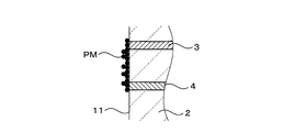
- FIG. 2 is a schematic cross-sectional view showing a configuration of detection electrodes of sensor elements in the first embodiment.
- FIG. FIG. 3 is an enlarged cross-sectional view of a region III in FIG.
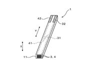
- FIG. 3 is an overall perspective view of the sensor element in the first embodiment.
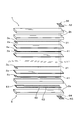
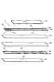
- FIG. 3 is a development view showing the entire configuration of the sensor element in the first embodiment.
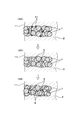
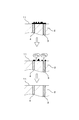
- FIG. 3 is a schematic cross-sectional view showing a sensor element manufacturing process and a change in detection electrode configuration after manufacturing in the first embodiment.
- FIG. 3 is a schematic diagram illustrating a process of removing PM after PM detection of the sensor element in the first embodiment.
- FIG. 4 is an overall perspective view of a sensor element in Embodiment 2.
- FIG. 1 The principal part expansion perspective view of the sensor element in Embodiment 1.
- FIG. 3 is an enlarged cross-sectional view of a region III in FIG.
- FIG. 3 is an overall perspective view of the
- FIG. 6 is a longitudinal sectional view of a sensor element in the second embodiment.
- FIG. 6 is a development view showing the entire configuration of a sensor element in Embodiment 2.
- the principal part expansion perspective view of the sensor element which shows the area
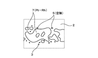
- FIG. FIG. 12 is a schematic diagram showing a cross-sectional structure of a region XII in FIG. 11, which is a cross section of a sensor element in the vicinity of a detection surface observed with a scanning electron microscope in Experimental Example 1.
- FIG. 6 is a cross-sectional view of a sensor element in the vicinity of a detection surface observed with a scanning electron microscope and an enlarged cross-sectional view thereof in a conventional element and Experimental Example 5, and a representative example in which Rh is alloyed among the metals shown in Experimental Example 5
- the measurement result of the electrode resistance change rate of the sensor element after the endurance test in Experimental Example 5 is shown in comparison with the conventional sensor element, and Rh is alloyed among the metals shown in Experimental Example 5.
- the present embodiment is an application example to a particulate matter detection sensor provided with a laminated sensor element 1.
- the particulate matter detection sensor is installed in, for example, an exhaust passage of an internal combustion engine and constitutes a part of the exhaust aftertreatment device.
- the sensor element 1 can detect particulate matter (hereinafter referred to as PM) as the specific substance contained in the gas to be measured.
- the gas to be measured is, for example, combustion exhaust gas discharged from an internal combustion engine, and includes minute PM made of conductive soot or the like.
- the sensor element 1 has a detection surface 11 at one end surface of the insulating substrate 2. On the detection surface 11, a part of the pair of detection electrodes 3 and 4 that are electrodes for the sensor element is exposed to form a linear electrode. The remaining portions of the detection electrodes 3 and 4 are embedded in the insulating substrate 2. As shown in FIG. 2, the detection electrode 3 and the detection electrode 4 having different polarities are each composed of a plurality of electrodes 3a and 4a. The electrodes 3a and 4a are alternately disposed on the insulating base 2 to constitute opposing electrode pairs. The plurality of electrodes 3 a and 4 a constituting the detection electrodes 3 and 4 are connected to the extraction electrodes 31 and 41 inside the insulating base 2.
- the extraction electrodes 31 and 41 extend from the detection surface 11 toward the end surface on the side facing the detection surface 11 inside the insulating substrate 2.
- the electrode 3a of the detection electrode 3 and the electrode 4a of the detection electrode 4 constituting each electrode pair have the same shape on the detection surface 11, and are arranged in parallel at a predetermined interval.
- interval and number of electrode pairs can be selected suitably.
- the exposed surfaces of the detection electrodes 3 and 4 are flush with one end surface of the insulating substrate 2 that becomes the detection surface 11.
- the surface of the insulating substrate 2 between the detection electrodes 3 and 4 serves as a PM collection surface.
- PM adheres to the detection surface 11 of the sensor element 1 and accumulates on the exposed surfaces of the detection electrodes 3 and 4 and the surface of the insulating substrate 2.
- the resistance value between the electrodes changes in accordance with the PM deposition amount.
- a current flows through the detection electrodes 3 and 4, and the PM deposition amount can be detected from the value of the detection current I.
- FIG. 1 As shown in FIG.
- the current flow direction is the longitudinal direction Y of the sensor element 1 orthogonal to the stacking direction X of the detection electrodes 3, 4, and the end surface on the detection surface 11 side of the detection electrodes 3, 4 and its end surface Is a direction connecting the end faces facing each other.
- a ceramic material excellent in electrical insulation and heat resistance or a known ceramic material is used as the material of the insulating base 2.
- the ceramic material include insulating materials such as alumina, magnesia, titania, and mullite.
- Known ceramic materials include a dielectric material obtained by mixing a high dielectric constant material such as barium titanate and alumina or zirconia.
- a conductive material whose main component is an alloy of at least one metal selected from the group consisting of Rh, Ru, Ir, Os, and Pd and Pt is used as the group consisting of Rh, Ru, Ir, Os, and Pd and Pt is used.
- the conductive material to be the detection electrodes 3 and 4 can include the known ceramic material as an aggregate.
- the insulating substrate 2 is made of alumina (ie, Al 2 O 3 ), and the detection electrodes 3 and 4 are made of an alloy of Pt and Rh (hereinafter referred to as Pt— Rh alloy).
- Pt— Rh alloy an alloy of Pt and Rh
- minute granular voids 5 are dispersedly arranged between the alloy particles 7 made of a Pt—Rh alloy or the like.
- the granular void 5 functions as an oxygen donating part that donates oxygen to a metal such as Rh contained in the alloy particle 7 to form a metal oxide 8 such as Rh 2 O 3 .
- the number of granular voids 5 per unit volume is preferably 3/100 ⁇ m 3 to 50/100 ⁇ m 3 .
- the number of granular voids 5 is in the above range in the entire current flow direction (that is, the direction orthogonal to the stacking direction X).
- the granular voids 5 are dispersed at a predetermined ratio throughout the detection electrodes 3 and 4 embedded in the insulating substrate 2.
- the metal oxide 8 such as Rh 2 O 3 is dispersedly formed on the entire detection electrodes 3 and 4.
- metals, such as Rh are spread
- the number of granular voids 5 per unit volume should be within the above range, and the conductive path by the alloy particles 7 such as a Pt—Rh alloy can be maintained.
- the number of the granular voids 5 is less than 3/100 ⁇ m 3, segregation of the metal oxide 8 on the surface of the detection surface 11 is not eliminated.
- the number of the granular voids 5 is larger than 50/100 ⁇ m 3 , the metal oxide 8 increases and the formation of a conductive path through which the detection current I flows is prevented.
- the content of the metal such as Rh in the Pt alloy is such that the content of the metal such as Rh is 40% by mass or less, preferably 0.5% by mass to 40% with respect to the total amount of Pt and the metal such as Rh. Desirably, it is in the range of 2% by mass to 30% by mass, more preferably 2% by mass.
- the size of the granular void 5 formed inside the detection electrodes 3 and 4 is usually sufficiently smaller than the average particle diameter of the alloy particles 7.
- the particle size of the granular void 5 is 5 ⁇ m or less, preferably 2.5 ⁇ m or less. If the particle size of the granular voids 5 is larger than 5 ⁇ m, the formation of the conductive path by the alloy particles 7 may be hindered.
- the detection electrodes 3 and 4 are divided into a central portion and both end portions in the stacking direction X of the detection electrodes 3 and 4 (that is, a direction orthogonal to the current flow direction), more particles are formed at both end portions.
- the gaps 5 are dispersedly arranged. That is, it is desirable that the degree of gap dispersion, which represents the deviation of the granular gap 5 inside the detection electrodes 3 and 4, is larger than 0.5.
- the void dispersion is a ratio of the number of granular voids 5 existing at both ends when the detection electrodes 3 and 4 are equally divided into the center and both ends.
- the number of voids at both ends of the detection electrodes 3 and 4 can be calculated as the total number of voids. Since the gap dispersion degree is larger than 0.5 and more granular gaps 5 are arranged at both ends of the detection electrodes 3 and 4, it becomes easier for current to flow through the central portion, and an increase in electrode resistance can be suppressed. .
- the void dispersity is in the range of 0.55 to 0.95.
- the insulating base 2 has a rectangular parallelepiped shape as a whole, and the end face on one end side in the longitudinal direction Y (that is, the end face on the near side of the insulating base 2 shown in FIG. 4) is the first face. And The end surface of the insulating base 2 shown in FIG. 4 facing the first surface is taken as the second surface. A detection surface 11 from which the detection electrodes 3 and 4 are exposed is provided on the first surface. Terminal electrodes 32 and 42 are arranged on the second surface and connected to a measurement unit (not shown). The terminal electrodes 32 and 42 are connected to the detection electrodes 3 and 4 via the extraction electrodes 31 and 41, respectively, inside the insulating substrate 2.
- the insulating base 2 is formed by laminating ceramic green sheets 2a and 2b made of the above-described ceramic material such as alumina.
- the electrodes 3a and 4a that become the detection electrodes 3 and 4 and the extraction electrodes 31 and 41 are opposed to each other with the ceramic green sheet 2a having a relatively thin sheet thickness interposed therebetween.
- the uppermost layer of the sensor element 1 is a ceramic green sheet of the sensor element 1 located on the uppermost side of the drawing of FIG.
- two ceramic green sheets 2b having a relatively large sheet thickness are disposed on the uppermost layer of the sensor element 1 or the lowermost layer facing the uppermost layer, respectively.
- the thickness of the ceramic green sheet 2a corresponds to the distance between the detection electrodes 3 and 4 and is set to a desired inter-electrode distance.
- Terminal electrodes 32 and 42 are formed on the surface of the ceramic green sheet 2 b which is the uppermost layer of the insulating substrate 2.
- a heater electrode 61 and extraction electrodes 62 and 63 are embedded between two ceramic green sheets 2b to form the heater portion 6.
- Terminal electrodes 64 and 65 for the heater section 6 are formed on the surface of the ceramic green sheet 2b, which is the lowest layer, at the end on the side facing the heater electrode 61.
- the heater electrode 61 is provided corresponding to the formation position of the electrodes 3a and 4a to be the detection electrodes 3 and 4, and the entire detection surface 11 can be heated.
- the particulate matter detection sensor energizes the heater unit 6 when the sensor element 1 is operated to remove moisture and PM adhering to the surface of the detection surface 11 to prevent detection errors.
- Such a laminated sensor element 1 is manufactured by a sheet forming step S1, an electrode printing step S2, a lamination step S3, a cutting step S4, and a firing step S5.
- the sheet forming step S1 a plurality of ceramic green sheets 2a and 2b are formed.
- the electrode printing step S2 the detection electrodes 3 and 4 are printed.
- the lamination step S3, the plurality of ceramic green sheets 2a and 2b are laminated.
- the cutting step S4 the laminate obtained in the lamination step S3 is cut into a predetermined shape.
- the firing step S5 the laminate is fired.
- the obtained sensor element becomes the sensor element 1 for the particulate matter detection sensor through the processing step S6 and the assembly step S7.
- the sheet forming step S1 an organic solvent and an organic binder are added to a powder of a ceramic material such as alumina to form a slurry. Then, the slurry is formed into a sheet having a predetermined thickness by a known doctor blade method and dried to obtain ceramic green sheets 2a and 2b.
- electrodes 3a and 4a to be the detection electrodes 3 or the detection electrodes 4 are formed on the surface of the ceramic green sheet 2a.
- alloy particles 7 such as Pt—Rh, aggregates such as alumina, void-forming particles for forming granular voids 5 such as resin beads, and paste-like electrode material may be used. It can.
- the paste-like electrode material is obtained by adding and mixing an organic solvent and an organic binder.
- electrode 3a, 4a can be formed so that it may become a predetermined pattern by screen printing, for example.
- the electrodes 3a and 4a to be the detection electrodes 3 and 4 are configured by the same rectangular electrode film, but two types of symmetrical electrode patterns may be employed.
- the resin beads which are void-forming particles, are spherical particles that are burned down by firing and form granular voids 5 around the alloy particles 7.
- the resin beads are melted and decomposed at the same temperature as the organic binder (for example, about 400 ° C.).
- resin beads made of a resin material having excellent solvent resistance retain the shape without being dissolved in a solvent used for a paste-like electrode material. For this reason, it is possible to easily adjust the void diameter and the number of voids.
- a plurality of electrodes are formed on the surface of the ceramic green sheet 2b so as to have a predetermined pattern, for example, by screen printing.
- the plurality of electrodes are the extraction electrodes 31 and 41, the terminal electrodes 32 and 42, the heater electrode 61, the extraction electrodes 62 and 63, or the terminal electrodes 64 and 65 for the heater section 6.
- the ceramic green sheets 2a and 2b are cut into a predetermined size in advance. Through holes for connecting the extraction electrodes 31 and 41 to the terminal electrodes 32 and 42 and the extraction electrodes 62 and 63 to the terminal electrodes 64 and 65 are provided at predetermined positions of the ceramic green sheets 2a and 2b. These through holes are filled with the same electrode material in the electrode printing step S2.
- the ceramic green sheets 2a and 2b are laminated in a predetermined order, and are pressed and pressed to form a laminated body.
- cutting process S4 the obtained block-shaped laminated body is cut
- the firing step S5 the laminate is degreased and then fired at a temperature equal to or higher than the sintering temperature of the ceramic material (for example, 1450 ° C.).
- resin beads 51 which are void-forming particles, are dispersed in the electrode films to be the detection electrodes 3 and 4.
- the resin beads 51 are melted and decomposed in the temperature rising process.
- the granular voids 5 are formed.
- the number of granular voids 5 included in the detection electrodes 3 and 4 can be adjusted by the amount of the resin beads 51 mixed.
- the size of the granular void 5 can be adjusted by the particle size of the resin beads 51.
- processing step S6 the detection surface 11 of the obtained fired body is polished to expose the detection electrodes 3 and 4 to obtain the sensor element 1.
- the sensor element 1 is further held in a mounting cylindrical housing (not shown) and covered with a cover body provided with a through hole to form a particulate matter detection sensor.
- the sensor element 1 manufactured in this way is used for a particulate matter detection sensor disposed on, for example, an exhaust gas outlet side of an exhaust gas purification filter provided in an exhaust passage of an internal combustion engine.
- the sensor element 1 detects PM in the combustion exhaust gas that has passed through the exhaust gas purification filter.
- the sensor element 1 can also be used for the particulate matter detection sensor arranged on the exhaust gas inlet side of the exhaust gas purification filter. In this case, PM in the combustion exhaust gas before passing through the exhaust gas purification filter can be detected.
- the exhaust gas purification filter may be a diesel particulate filter (ie, DPF) or a gasoline particulate filter (ie, GPF).
- the particulate matter detection sensor including the sensor element 1 may be used for detecting PM contained in combustion exhaust gas exhausted from a diesel engine. Moreover, you may use in order to detect PM contained in the combustion exhaust gas exhausted from a gasoline engine.
- S8 is a process of PM detection and PM removal, and after this PM detection, the process of removing the deposited PM is repeated.
- the detection electrodes 3 and 4 are exposed on the detection surface 11, are opposed to each other with the insulating base 2 interposed therebetween, and are exposed to the combustion exhaust gas flowing through the exhaust passage.
- a predetermined voltage is applied between the detection electrodes 3 and 4 to form an electrostatic field, and PM is attracted and deposited on the surface of the detection surface 11.
- the PMs are continuously connected between the detection electrodes 3 and 4. From this state, in order to remove PM, the heater section 6 of the sensor element 1 is energized, and the surface of the detection surface 11 is heated to a temperature at which PM can be combusted or higher (for example, 750 ° C.). Thereby, as shown in the figure in FIG. 7, PM containing carbon as a main component burns, CO 2 is released, and PM is removed from the detection surface 11 as shown in the lower figure of FIG. 7.
- the heating temperature in PM removal in S8 is a temperature at which a metal such as Rh contained in the Pt—Rh alloy constituting the detection electrodes 3 and 4 is oxidized. Therefore, as shown in FIG. 6, a metal oxide 8 (Rh 2 O 3 ) in which Rh is oxidized is generated in the detection electrodes 3 and 4. At this time, Rh 2 O 3 is generated not only on the detection surface 11 exposed to the gas to be measured, but also at a site in contact with the granular void 5 serving as an oxygen donating portion, so that segregation of Rh 2 O 3 does not occur.
- the sensor element 1 has a laminated electrode structure in which the electrode films of the plurality of detection electrodes 3 and 4 are embedded in layers inside the insulating substrate 2. A part of the plurality of pairs of detection electrodes 3 and 4 is a first group, and the remaining pair of detection electrodes 3 and 4 is a second group. As shown in Embodiment 2 in FIGS. 8 to 10, in the sensor element 1, the first group is printed on the surface to be the detection surface 11 of the insulating substrate 2, and the printing group in which the second group is embedded. It can also be set as the electrode structure.
- the basic configuration of the sensor element 1 is the same as that of the first embodiment, and the difference from the first embodiment will be mainly described below.
- the sensor element 1 has a flat rectangular parallelepiped insulating base 2.
- a part of the upper surface of the insulating substrate 2 (that is, the upper surface on the front side of the insulating substrate 2 shown in FIG. 8 and the upper surface on the left side of the insulating substrate 2 shown in FIGS. 9 and 10) is used as the detection surface 11.
- the heater unit 6 is disposed on the side facing the detection surface 11.
- the pair of detection electrodes 3 and 4 includes detection units 33 and 43 including a pair of comb-like electrodes disposed on the detection surface 11, and lead portions 34 and 44.
- the lead portions 34 and 44 are embedded in the insulating base 2.
- the terminal electrodes 32 and 42 are formed on a part of the upper surface of the insulating substrate 2 (that is, the upper surface on the back side in FIG. 8 and the upper surface on the right side in FIGS. 9 and 10).
- Lead-out parts 34 and 44 extending along the longitudinal direction Y of the insulating base 2 connect the detection parts 33 and 43 and the terminal electrodes 32 and 42.
- the detection units 33 and 43 are comb-like electrodes each having a plurality of linear electrodes. The plurality of linear electrodes are connected at one end side and connected to the lead-out portions 34 and 44.
- the insulating base 2 is configured by laminating ceramic green sheets 2 a and 2 b having different sheet thicknesses, for example.
- a plurality of ceramic green sheets 2a having a relatively small sheet thickness are arranged with a ceramic green sheet 2b having a relatively large sheet thickness interposed therebetween.
- the pair of detection electrodes 3 and 4 and the terminal electrodes 32 and 42 are formed on the surface of the ceramic green sheet 2a located immediately above the ceramic green sheet 2b.
- a ceramic green sheet 2 a that covers the upper surfaces of the lead portions 34 and 44 is disposed on the uppermost layer of the insulating substrate 2.
- the detection electrodes 3 and 4 can be formed by screen printing or the like using an alloy particle 7 such as Pt—Rh, an aggregate such as alumina, and an electrode material so as to form a predetermined pattern. it can.
- the electrode material includes void-forming particles.
- a heater electrode 61 and extraction electrodes 62 and 63 serving as the heater section 6 are embedded. These electrodes are connected to terminal electrodes 64 and 65 formed exposed on the lower surface of the ceramic green sheet 2b.
- the heater electrode 61, the extraction electrodes 62 and 63, and the terminal electrodes 64 and 65 can be formed by screen printing or the like using a normal electrode material so as to form a predetermined pattern.
- Detecting electrodes 3 and 4 terminal electrodes 32 and 42, heater electrodes 61, extraction electrodes 62 and 63, and terminal electrodes 64 and 65 were printed on these ceramic green sheets 2 a and 2 b to be the insulating base 2. Thereafter, the ceramic green sheets 2a and 2b are stacked in a predetermined order and integrally fired, whereby the sensor element 1 is formed.
- the lead-out portions 34 and 44 that form part of the detection electrodes 3 and 4 are embedded in the insulating base 2. Even in such a configuration, the same effect as that of the first embodiment can be obtained by setting the granular void 5 existing inside the detection electrodes 3 and 4 within the predetermined range. That is, the metal such as Rh serving as the electrode material is prevented from diffusing from the lead portions 34 and 44 to the detection portions 33 and 43. The detection units 33 and 43 are exposed on the detection surface 11. And it can suppress that the distance between electrodes changes at the time of the temperature rise by the removal process after PM detection.
- the sensor element 1 of Embodiment 1 was produced by the method described above, and an endurance test was performed to examine changes in the electrode resistance values of the detection electrodes 3 and 4.
- An electrode material was used for the detection electrodes 3 and 4.
- the electrode material was obtained by adding void-forming particles made of resin beads to alloy particles 7 made of a Pt—Rh alloy, aggregate made of alumina, and electrode paste.
- the electrode paste is obtained by mixing and kneading an organic solvent and an organic binder.
- the alloy particles 7 were prepared by mixing an acid solution containing Pt ions and Rh ions and performing a reduction reaction with a reducing agent.
- Pt was changed in the range of 98 mass% to 69 mass% and Rh: 2 mass% to 31 mass%. This is a blending ratio when the total amount of Pt and Rh is 100% by mass.
- the amount of resin beads used as void-forming particles added to the electrode paste is increased or decreased.
- the number of granular voids 5 per unit volume as shown in Table 1, can be varied in a range of 3/100 [mu] m 3 ⁇ 79 pieces / 100 [mu] m 3 (i.e., Examples 1-11 Comparative Examples 1 and 2).
- the number of the granular voids 5 is a value converted into the number per unit volume by preparing a three-dimensional image of the detection electrodes 3 and 4 and observing the granular voids 5 included therein.
- a three-dimensional scanning electron microscope (hereinafter referred to as 3D-SEM) and an energy dispersive X-ray spectrometer (hereinafter referred to as EDX) were used for observation and three-dimensional image preparation.
- the void diameter is an average diameter (unit: ⁇ m) of the granular void 5, and is an average value obtained by measuring the particle diameter of 30 granular voids 5 using a 3D image by 3D-SEM and EDX. .
- FIGS. 11 to 13 for example, as shown in FIGS. The electrode cross section was divided into four in the stacking direction X (that is, the direction orthogonal to the current flow direction). Then, the ratio of the number of voids at both ends to the total number of voids (that is, the number of voids at both ends / total number of voids) was calculated.
- Rate of change in electrode resistance (electrode resistance value after endurance / initial electrode resistance value) ⁇ 100 Durability evaluation, electrode resistance change rate, Shun good the case is less than 10 ⁇ 10 2%, and allowed to be a 10 ⁇ 10 2% ⁇ 40 ⁇ 10 2%, more than 40 ⁇ 10 2% The case was disabled.
- Example 2 In the same manner as in Experimental Example 1, a sensor element 1 was manufactured under the following conditions, and Examples 12 to 15 and Comparative Examples 3 and 4 were obtained.
- the number of granular void 5 is in the range of 19/100 [mu] m 3 ⁇ 28 pieces / 100 [mu] m 3, (2) mixing ratio of Pt and Rh, Pt: 100% to 39 wt%, Rh: 0 wt% The range of ⁇ 61% by mass.
- These Examples 12 to 15 and Comparative Examples 3 to 5 were subjected to the same durability test as in Experimental Example 1. And the result of having measured the change of the electrode resistance value of the detection electrodes 3 and 4 is shown in Table 2 with a space
- Comparative Example 3 In Table 2, in Comparative Example 3, the detection electrodes 3 and 4 are reduced from the detection surface 11 of the sensor element 1 and disappear toward the inside of the insulating substrate. Thereby, the electrode resistance value after an endurance test became impossible to measure. Comparative Example 3 does not contain Rh in Pt. In addition, the rate of change in electrode resistance increases with an increase in the mixing ratio of Rh to Pt. In Comparative Examples 4 and 5 in which the content of Rh exceeds 40% by mass, the electrode resistance value after the durability test increases, and sufficient durability is not obtained.
- Step (b) is a step of heating to a high temperature in order to oxidize and remove PM adhering to the detection surface 11 of the sensor element 1. Therefore, when the PM removal shown in (c) is completed, the detection electrodes 3 and 4 disappear from the detection surface 11 toward the inside of the insulating substrate while being reduced. In the step (d), when detecting PM again, the actual inter-electrode distance becomes longer than the initial state.
- the detection time until the detected current reaches the specified value becomes longer as indicated by the dotted line B with respect to the detected current characteristic A in the initial state indicated by the solid line in FIG.
- the detection time becomes longer as indicated by the dotted line C exceeds the specified time t, and cannot be detected.
- Example 3 In the same manner as in Experimental Example 1, the sensor element 1 was manufactured under the following conditions, and Examples 16 to 25 were obtained.
- the number of granular voids 5 of Pt and Rh is in the range of 19/100 [mu] m 3 ⁇ 28 pieces / 100 [mu] m 3, (2) size range of 0.3 [mu] m ⁇ 4.8 .mu.m particulate void 5, (3 ) Void dispersion degree is in the range of 0.49 to 0.79.
- the same durability test was performed, and the results of measuring the change in the electrode resistance value of the detection electrodes 3 and 4 are shown in Table 3 together with the blending ratio of Pt and Rh.
- Example 4 In the same manner as in Experimental Example 1, a sensor element 1 was produced under the following conditions, and Examples 26 to 35 were obtained.
- the number of granular voids 5 of Pt and Rh is in the range of 19/100 [mu] m 3 ⁇ 28 pieces / 100 [mu] m 3, (2) size range of 0.9 .mu.m ⁇ 4.1 .mu.m particulate void 5, (3 )
- the void dispersion is in the range of 0.51 to 0.95.
- the same durability test was performed, and the results of measuring the change in the electrode resistance value of the detection electrodes 3 and 4 are shown in Table 4 together with the blend ratio of Pt and Rh.
- Example 5 Next, the effect of Pt on the volatilization of Pt and the following metal was used as the electrode material of the detection electrodes 3 and 4 in place of the alloy of Pt and Rh.
- the metal is a metal selected from at least one selected from Rh, Ru, Ir, Os and Pd.
- an alloy of Pt and these metals, an aggregate, and an electrode paste were used, and the sensor element 1 was produced by the same method as in Experimental Example 1.
- the electrode paste is obtained by mixing and kneading an organic solvent and an organic binder.
- a sensor element 1 was produced in the same manner using an electrode material having a Pt of 100% by mass.
- the obtained sensor element 1 was subjected to a high temperature durability test. First, each sensor element 1 was heated at a temperature of 900 ° C. for 250 hours. Thereafter, the distance between the detection electrodes 3 and 4 on the detection surface 11 was measured, and the rate of change from the distance before the high temperature durability test was calculated. In the evaluation, a case where the rate of change was 0% was evaluated as good, a case where the rate of change exceeded 0% and 5% or less was evaluated as acceptable, and a case where the rate of change exceeded 5% was regarded as impossible.
- the sensor element 1 having a Pt of 100% by mass had a rate of change of more than 5% and was evaluated as being impossible.
- the sensor element 1 using an alloy of Pt and Rh, Ru, Ir, or Os had a change rate of 0%, and good results were obtained.
- the sensor element 1 using an alloy of Pt and Pd has a rate of change of 5% or less, and although slightly inferior to other metals, an effect of suppressing Pt volatilization was observed.
- “Before measures” shown in FIG. 18 is a conventional sensor element, and resin beads are not added to the electrode material.
- the sensor element 1 manufactured by adding resin beads to the electrode material as in Experimental Example 1 before the countermeasure.
- the sensor element using an alloy of Pt and Rh in the above test example was adjusted to a range of 19/100 ⁇ m 3 to 28/100 ⁇ m 3 .
- an endurance test was performed and the rate of change in electrode resistance was measured.
- FIG. 17 it was confirmed that the granular void 5 was formed inside the electrode of the sensor element 1 as compared with the conventional element.
- Example 37 in which the granular voids 5 were formed, the rate of change in electrode resistance was reduced and the durability was improved.
- the metal oxide 8 is generated not only in the detection surface 11 but also in the electrode by oxygen donation from the granular void 5 in the electrode. Therefore, the difference in Rh concentration in the electrode alloy is reduced between the outermost surface of the detection electrodes 3 and 4 and the inside thereof, and the diffusion amount of Rh to the outermost electrode surface is reduced. As a result, the production amount of the metal oxide 8 on the outermost surface of the electrode exposed on the detection surface 11 is reduced, and the rate of increase in the resistance value on the outermost surface portion of the electrode is reduced. Thereby, volatilization of Pt in the detection electrodes 3 and 4 can be suppressed, and the overall resistance value increase rate of the detection electrodes 3 and 4 can be suppressed low.
- the electrode for sensor element and the sensor element 1 of the present invention are not limited to the above-described embodiment and the above-described examples, and various modifications can be made without departing from the spirit of the present invention.
- the application example to the particulate matter detection sensor for detecting the particulate matter contained in the combustion exhaust gas of the internal combustion engine has been described, but the gas to be measured containing the particulate matter is the combustion exhaust gas.
- the gas to be measured containing the particulate matter is the combustion exhaust gas.
- it may be used for purposes other than failure diagnosis of post-processing devices such as DPF.
- it can of course be applied to a sensor element having a similar detection electrode structure and detecting a substance other than the particulate substance.
- the sensor element 1 is not limited to the one described in the above embodiment, and may be any configuration as long as it has a detection surface 11 where a part of the detection electrodes 3 and 4 is exposed on the surface of the insulating substrate 2.
- the shape of the insulating substrate 2 and the detection electrodes 3 and 4 of the sensor element 1 can be changed as appropriate.
Landscapes
- Chemical & Material Sciences (AREA)
- Physics & Mathematics (AREA)
- General Physics & Mathematics (AREA)
- General Health & Medical Sciences (AREA)
- Immunology (AREA)
- Life Sciences & Earth Sciences (AREA)
- Analytical Chemistry (AREA)
- Biochemistry (AREA)
- Pathology (AREA)
- Health & Medical Sciences (AREA)
- Chemical Kinetics & Catalysis (AREA)
- Electrochemistry (AREA)
- Dispersion Chemistry (AREA)
- Engineering & Computer Science (AREA)
- Combustion & Propulsion (AREA)
- Investigating Or Analyzing Materials By The Use Of Electric Means (AREA)
- Measuring Oxygen Concentration In Cells (AREA)
Abstract
被測定ガス中の特定物質を検出するセンサ素子1用電極であって、上記特定物質が付着する検出面11を有する絶縁性基体2に、上記検出面に一部が露出するように埋設されており、Rh、Ru、Ir、Os及びPdからなるグループから選ばれる少なくとも1種の金属とPtとの合金7と、該合金間に分散配置された粒状空隙5と、を有し、上記合金中の上記金属の含有量が40質量%以下であると共に、上記センサ素子用電極の単位体積あたりの上記粒状空隙の個数が、3個/100μm3~50個/100μm3である。
Description
本発明は、粒子状物質検出センサ等に用いられるセンサ素子用電極と、それを用いたセンサ素子に関する。
内燃機関から排出される排ガス中の粒子状物質(すなわち、Particulate Matter:PM)の量を検出するために、電気抵抗式の粒子状物質検出センサが使用されている。粒子状物質検出センサは、絶縁性基体と、該絶縁性基体に少なくとも一部が埋設された検出電極を有する。そして、検出電極が露出する、絶縁性基体の端面又は側面を検出面とするセンサ素子を備えている。
このようなセンサ素子の検出面には、異なる極性の検出電極が、絶縁層を挟んで交互に配設される。これら電極間に電圧を印加することで、静電場が形成される。これにより、帯電した粒子状物質が静電場に引き寄せられて検出面に捕集され、電極間が導通する。したがって、電極間の抵抗値の変化から、排ガスに含まれる粒子状物質の量を検出することができる。
一般に、検出電極には、Pt電極が用いられる。各種センサ用のPt又はPt合金からなるセンサ用電極は、例えば、特許文献1に開示されている。また、粒子状物質検出センサ用の検出電極として、特許文献2には、Ptと軟化温度が1000℃以上のガラス材料とからなる電極が開示されている。
特許文献1等に記載される、従来のPt電極は、骨材となるセラミック粒子相を含むことから多孔質となる。そして、Pt電極において、高温条件下(例えば850℃以上)でPtの酸化による揮散が生じやすい。そのため、Pt電極を粒子状物質検出センサに適用した場合には、Ptが酸化して蒸気圧の低いPtO2となり、検出面から揮散して消失してしまうおそれがある。その結果、検出電極が縮小しながら検出面から絶縁性基体の内部に向かって消失していき、検出面に露出しなくなると、電極間距離が長くなって、検出精度が低下する。
一方、特許文献2では、ガラス材料を添加することにより、熱処理時に孔や隙間を埋めて、Ptの揮散を抑制している。しかしながら、ガラス材料の添加は、電極としての抵抗値上昇につながる。このように現状では、Ptの揮散・消失による検出電極の縮小を抑制しつつ、所望の電極抵抗値を実現することは難しい。
本発明は、かかる背景に鑑みてなされたものであり、検出面におけるPtの揮散と、電極抵抗値の上昇とを共に抑制して、検出精度を向上させるセンサ素子用電極及びそれを用いたセンサ素子を提供しようとするものである。
本発明の一態様は、被測定ガス中の特定物質を検出するセンサ素子(1)用電極であって、
上記特定物質が付着する検出面(11)を有する絶縁性基体(2)に、上記検出面に一部が露出するように埋設されており、
Rh、Ru、Ir、Os及びPdからなるグループから選ばれる少なくとも1種の金属とPtとの合金(7)と、該合金間に分散配置された粒状空隙(5)と、を有し、
上記合金中の上記金属の含有量が40質量%以下であると共に、上記センサ素子用電極の単位体積あたりの上記粒状空隙の個数が、3個/100μm3~50個/100μm3である、センサ素子用電極にある。
上記特定物質が付着する検出面(11)を有する絶縁性基体(2)に、上記検出面に一部が露出するように埋設されており、
Rh、Ru、Ir、Os及びPdからなるグループから選ばれる少なくとも1種の金属とPtとの合金(7)と、該合金間に分散配置された粒状空隙(5)と、を有し、
上記合金中の上記金属の含有量が40質量%以下であると共に、上記センサ素子用電極の単位体積あたりの上記粒状空隙の個数が、3個/100μm3~50個/100μm3である、センサ素子用電極にある。
本発明の他の態様は、被測定ガス中の特定物質を検出するセンサ素子(1)であって、
上記特定物質が付着する検出面(11)を有する絶縁性基体(2)と、
上記検出面に一部が露出して対向位置し、残部が上記絶縁性基体に埋設される、極性の異なる一対の検出電極(3、4)と、を備えており、
上記検出電極は、Rh、Ru、Ir、Os及びPdからなるグループから選ばれる少なくとも1種の金属とPtとの合金(7)と、該合金間に分散配置された粒状空隙(5)と、を有し、
上記合金中の上記金属の含有量が40質量%以下であると共に、上記検出電極の単位体積あたりの上記粒状空隙の個数が、3個/100μm3~50個/100μm3である、センサ素子にある。
なお、括弧内の符号は、参考のために付したものであり、本発明はこれら符号により限定されるものではない。
上記特定物質が付着する検出面(11)を有する絶縁性基体(2)と、
上記検出面に一部が露出して対向位置し、残部が上記絶縁性基体に埋設される、極性の異なる一対の検出電極(3、4)と、を備えており、
上記検出電極は、Rh、Ru、Ir、Os及びPdからなるグループから選ばれる少なくとも1種の金属とPtとの合金(7)と、該合金間に分散配置された粒状空隙(5)と、を有し、
上記合金中の上記金属の含有量が40質量%以下であると共に、上記検出電極の単位体積あたりの上記粒状空隙の個数が、3個/100μm3~50個/100μm3である、センサ素子にある。
なお、括弧内の符号は、参考のために付したものであり、本発明はこれら符号により限定されるものではない。
上記センサ素子用電極は、Ptと上記金属との合金を主成分とすることで、高温域で検出面からPtが揮散して消失するのを抑制する効果が得られる。しかし、電極の主成分を合金とするだけでは、高温域(例えば700℃~800℃の範囲)において、内部の上記金属が検出面に偏析して抵抗層を形成し、電極抵抗値が上昇することが判明した。なお、上記高温域において、上記金属は最表層の金属も酸化する。これに対して、上記センサ素子用電極においては、合金間に分散配置された粒状空隙により、上記金属の偏析をも抑制できる。すなわち、上記センサ素子用電極の内部に、粒状空隙を3個/100μm3~50個/100μm3の範囲で存在させることで、粒状空隙に接する上記金属の酸化が生じる。その結果、上記金属の電極表面への拡散、さらには酸化物の検出面への偏析が抑制される。また、電極抵抗値の上昇率を小さくすることが可能になる。
上記センサ素子用電極は、Ptの揮散・消失の抑制と、電極抵抗値の上昇の抑制とを両立させることができる。したがって、センサ素子は、検出面における電極間隔の変化が抑制され、電極抵抗値を低く維持して、検出精度を向上させる。センサ素子は、上記センサ素子用電極を上記一対の検出電極とする。
(実施形態1)
次に、センサ素子用電極及びそれを用いたセンサ素子の実施形態について、図面を参照して説明する。本形態は、図1~図5に示すように、積層型のセンサ素子1を備えた、粒子状物質検出センサへの適用例である。粒子状物質検出センサは、例えば、内燃機関の排気通路に設置されて排気後処理装置の一部を構成する。そして、センサ素子1により、被測定ガスに含まれる特定物質として、粒子状物質(以下、PMと称する)を検出することができる。被測定ガスは、例えば、内燃機関から排出される燃焼排ガスであり、導電性を有する煤等からなる微小なPMを含んでいる。
次に、センサ素子用電極及びそれを用いたセンサ素子の実施形態について、図面を参照して説明する。本形態は、図1~図5に示すように、積層型のセンサ素子1を備えた、粒子状物質検出センサへの適用例である。粒子状物質検出センサは、例えば、内燃機関の排気通路に設置されて排気後処理装置の一部を構成する。そして、センサ素子1により、被測定ガスに含まれる特定物質として、粒子状物質(以下、PMと称する)を検出することができる。被測定ガスは、例えば、内燃機関から排出される燃焼排ガスであり、導電性を有する煤等からなる微小なPMを含んでいる。
図1~図3に示すように、センサ素子1は、絶縁性基体2の一端面を検出面11としている。検出面11には、センサ素子用電極である一対の検出電極3、4の一部が露出して線状電極が形成されている。検出電極3、4の残部は、絶縁性基体2に埋設されている。図2に示すように、極性の異なる検出電極3と検出電極4は、それぞれ複数の電極3a、4aからなる。それら電極3a、4aが交互に絶縁性基体2に配設されて、対向する電極対を構成している。検出電極3、4を構成する複数の電極3a、4aは、絶縁性基体2の内部において引出電極31、41に接続されている。引出電極31、41は、絶縁性基体2の内部を、検出面11から検出面11とは対向する側の端面へ向けて延びている。各電極対を構成する検出電極3の電極3aと検出電極4の電極4aは、検出面11において同一形状であり、所定間隔で平行に配置される。電極対の間隔や数は、適宜選択することができる。
図3に示すように、検出電極3、4の露出表面は、検出面11となる絶縁性基体2の一端面と面一となっている。検出電極3、4の間の絶縁性基体2の表面は、PMの捕集面となる。PMは、センサ素子1の検出面11に付着して、検出電極3、4の露出表面と絶縁性基体2の表面に堆積していく。電極対を構成する隣り合う検出電極3、4の間がPMを介して電気的に接続されると、PM堆積量に応じて電極間の抵抗値が変化する。このとき、図1中に矢印で示すように、検出電極3、4内を電流が流れ、検出電流Iの値からPM堆積量を検出することができる。電流の流れ方向は、図4に示すように、検出電極3、4の積層方向Xと直交するセンサ素子1の長手方向Yであり、検出電極3、4の検出面11側の端面とその端面と向かい合う端面とを結ぶ方向である。
絶縁性基体2の材質としては、電気絶縁性及び耐熱性に優れたセラミックス材料や公知のセラミック材料が用いられる。セラミックス材料は、例えば、アルミナ、マグネシア、チタニア、ムライト等の絶縁材料が挙げられる。公知のセラミック材料はチタン酸バリウム等の高誘電率材料とアルミナやジルコニアを混合した誘電体材料等が挙げられる。検出電極3、4の材質としては、Rh、Ru、Ir、Os及びPdからなるグループから選ばれる少なくとも1種の金属とPtとの合金を主成分とする導電性材料が用いられる。検出電極3、4となる導電性材料は、骨材として上記公知のセラミック材料を含むことができる。
好適には、図1中に示すように、例えば、絶縁性基体2をアルミナ(すなわち、Al2O3)で構成し、検出電極3、4を、PtとRhとの合金(以下、Pt-Rh合金と称する)で構成することができる。検出電極3、4の内部において、Pt-Rh合金等からなる合金粒子7同士の間には、微小な粒状空隙5が分散配置される。本形態において、粒状空隙5は、合金粒子7に含まれるRh等の金属に酸素を供与して、Rh2O3等の金属酸化物8を形成する、酸素供与部として機能する。この機能を得るために、単位体積あたりの粒状空隙5の個数は、3個/100μm3~50個/100μm3であるとよい。好ましくは、電流流れ方向(すなわち、積層方向Xと直交する方向)の全体において、粒状空隙5の個数が上記範囲にあるとよい。
絶縁性基体2に埋設される検出電極3、4の全体に、粒状空隙5が所定の割合で分散して存在する。これにより、検出電極3、4の全体に、Rh2O3等の金属酸化物8が分散形成される。これにより、Rh等の金属が、検出面11へ拡散して表面に金属酸化物8が偏析することが抑制される。この効果を得るには、単位体積あたりの粒状空隙5の個数を上記範囲にするのがよく、Pt-Rh合金等の合金粒子7による導電パスが維持される。粒状空隙5の個数が3個/100μm3より少ないと、検出面11の表面の金属酸化物8の偏析が解消されない。粒状空隙5の個数が50個/100μm3より多いと、金属酸化物8が多くなり、検出電流Iが流れる導電パスの形成を妨げる。
Pt合金中のRh等の金属の含有量は、PtとRh等の金属との合計量に対して、Rh等の金属の含有量が、40質量%以下、好ましくは0.5質量%~40質量%、より好ましくは2質量%~30質量%の範囲にあることが望ましい。また、検出電極3、4の内部に形成される粒状空隙5の大きさは、通常、合金粒子7の平均粒径に対して十分小さい。例えば、粒状空隙5の粒径は、5μm以下、好適には、2.5μm以下であることが望ましい。粒状空隙5の粒径が、5μmより大きいと、合金粒子7による導電パスの形成を妨げるおそれがある。
好適には、検出電極3、4の積層方向X(すなわち、電流流れ方向と直交する方向)において、検出電極3、4を中央部と両端部とに分割したときに、両端部により多くの粒状空隙5が分散配置されるとよい。つまり、検出電極3、4の内部における粒状空隙5の偏りを表わす、空隙分散度が、0.5より大きいことが望ましい。空隙分散度は、検出電極3、4を中央部と両端部に等分割したときに、両端部に存在する粒状空隙5の個数の全体に対する比率である。例えば、電流流れ方向(すなわち、積層方向Xと直交する方向)の電極断面において、検出電極3、4の両端部の空隙個数/総空隙個数として算出することができる。空隙分散度が0.5より大きく、検出電極3、4の両端部により多くの粒状空隙5が配置されることで、中央部により電流が流れやすくなり、電極抵抗の上昇を抑制することができる。好ましくは、空隙分散度が0.55~0.95の範囲にあるとよい。
図4に示すように、絶縁性基体2は、全体が直方体形状で、その長手方向Yの一端側の端面(すなわち、図4に示す絶縁性基体2の手前側の端面)を第1の面とする。第1の面と対向している、図4に示されている絶縁性基体2の端面を第2の面とする。第1の面には検出電極3、4が露出する検出面11が設けられる。第2の面には、端子電極32、42が配置されて、図示しない測定部に接続される。端子電極32、42は、絶縁性基体2の内部において、検出電極3、4と、それぞれ引出電極31、41を介して接続している。
図5に示すように、絶縁性基体2は、上述したアルミナ等のセラミックス材料からなるセラミックグリーンシート2a、2bを積層して構成される。検出電極3、4となる電極3a、4a、引出電極31、41は、それぞれ比較的シート厚の薄いセラミックグリーンシート2aを挟んで対向配置される。センサ素子1の最上層を、図5の図面の最も上側に位置するセンサ素子1のセラミックグリーンシートとする。センサ素子1の最上層又は最上層と対向する最下層には、比較的シート厚の厚いセラミックグリーンシート2bが、例えば、それぞれ2枚配置される。セラミックグリーンシート2aの厚さは、検出電極3、4の距離に相当し、所望の電極間距離となるように設定される。絶縁性基体2の最上層となるセラミックグリーンシート2bの表面には、端子電極32、42が形成される。
センサ素子1の最下層には、2枚のセラミックグリーンシート2bの間に、ヒータ電極61と引出電極62、63が埋設されて、ヒータ部6が形成される。ヒータ電極61と対向する側の端部において、最下層となるセラミックグリーンシート2bの表面には、ヒータ部6用の端子電極64、65が形成される。ヒータ電極61は、検出電極3、4となる電極3a、4aの形成位置に対応して設けられ、検出面11全体を加熱可能となっている。粒子状物質検出センサは、センサ素子1の作動時にヒータ部6に通電して、検出面11の表面に付着する水分やPMを除去し、検出誤差を防止する。
このような積層型のセンサ素子1は、シート形成工程S1と電極印刷工程S2と、積層工程S3と切断工程S4と焼成工程S5とにより製造される。シート形成工程S1は、複数のセラミックグリーンシート2a、2bを形成する。電極印刷工程S2は検出電極3、4を印刷する。積層工程S3は上記複数のセラミックグリーンシート2a、2bを積層する。切断工程S4は積層工程S3で得られた積層体を所定形状に切断する。焼成工程S5は積層体を焼成する。得られたセンサ素子は、加工工程S6、組付け工程S7を経て、粒子状物質検出センサ用のセンサ素子1となる。以下に、図6を参照しながら、センサ素子1の製造工程について、詳述する。
シート形成工程S1では、アルミナ等のセラミックス材料の粉末に有機溶媒と有機バインダを添加してスラリー状とする。そして、そのスラリー状物を公知のドクターブレード法により所定厚のシート状に成形し、乾燥して、セラミックグリーンシート2a、2bとする。次いで、電極印刷工程S2において、セラミックグリーンシート2aの表面に、検出電極3又は検出電極4となる電極3a、4aを形成する。
電極3a、4aの材料として、Pt-Rh等の合金粒子7と、アルミナ等の骨材と、粒状空隙5を形成するための空隙形成粒子、例えば樹脂ビーズと、ペースト状の電極材料用いることができる。ペースト状の電極材料は有機溶媒及び有機バインダを添加、混合したものである。そして、例えばスクリーン印刷により所定のパターンとなるように電極3a、4aを形成することができる。ここでは、検出電極3、4となる電極3a、4aを、長方形状の同一パターンの電極膜で構成するが、対称形状の2種類の電極パターンを採用することもできる。
ここで、空隙形成粒子である樹脂ビーズは、焼成により焼失して合金粒子7の周囲に粒状空隙5を形成する球状粒子である。そして、樹脂ビーズは、有機バインダと同等の温度(例えば、400℃程度)で、溶融分解する。具体的には、例えば、耐溶剤性に優れる樹脂材料からなる樹脂ビーズは、ペースト状の電極材料に使用される溶剤に溶解することなく、形状を保持する。このため、空隙径や空隙個数の調整が容易にできる。
同様にして、セラミックグリーンシート2bの表面に、複数の電極を、例えばスクリーン印刷により所定のパターンとなるように形成する。上記複数の電極とは、引出電極31、41、端子電極32、42、ヒータ電極61、引出電極62、63、又はヒータ部6用の端子電極64、65である。なお、セラミックグリーンシート2a、2bは、予め所定のサイズに切断される。セラミックグリーンシート2a、2bの所定位置には、引出電極31、41を端子電極32、42に、引出電極62、63を端子電極64、65に、それぞれ接続するためのスルーホールが設けられる。これらスルーホール内には、電極印刷工程S2において、同様の電極材料が充填される。
積層工程S3では、これらセラミックグリーンシート2a、2bを所定の順に積層し、加圧、圧着して積層体とする。切断工程S4では、得られたブロック状の積層体を、切断機又はダイシングにより、センサ素子1の形状に合わせて切断する。焼成工程S5では、積層体を脱脂後、セラミック材料の焼結温度以上で焼成する(例えば、1450℃)。
図6中に示すように、積層工程S3により得られた積層体において、検出電極3、4となる電極膜中には、空隙形成粒子である樹脂ビーズ51が分散している。焼成工程S5において、この積層体を焼成すると、昇温過程で樹脂ビーズ51が溶融分解する。そして、樹脂ビーズが焼失した後に、粒状空隙5が形成される。検出電極3、4中に含まれる粒状空隙5の数は、樹脂ビーズ51の混合量によって、調整することができる。また、粒状空隙5の大きさは、樹脂ビーズ51の粒径によって、調整することができる。
加工工程S6では、得られた焼成体の検出面11を研磨することで、検出電極3、4を露出させて、センサ素子1を得る。組付け工程S7では、さらに、図示しない取付用の筒状ハウジング内にセンサ素子1を保持し、通孔を設けたカバー体で覆って、粒子状物質検出センサとする。
このようにして製造されるセンサ素子1は、内燃機関の排気通路に設けられる排ガス浄化フィルタの、例えば排ガスの流出口側に配置される粒子状物質検出センサに用いられる。そして、センサ素子1は排ガス浄化フィルタを通過した燃焼排ガス中のPMを検出する。また、排ガス浄化フィルタの、排ガスの流入口側に配置される粒子状物質検出センサに、センサ素子1を用いることもできる。この場合には、排ガス浄化フィルタを通過する前の燃焼排ガス中のPMを検出できる。
排ガス浄化フィルタは、ディーゼルパティキュレートフィルタ(すなわち、DPF)であっても、ガソリンパティキュレートフィルタ(すなわち、GPF)であってもよい。センサ素子1を備える粒子状物質検出センサは、ディーゼルエンジンから排気される燃焼排ガス中に含まれるPMを検出するために用いられてもよい。また、ガソリンエンジンから排気される燃焼排ガス中に含まれるPMを検出するために用いられてもよい。
排ガス浄化フィルタは、ディーゼルパティキュレートフィルタ(すなわち、DPF)であっても、ガソリンパティキュレートフィルタ(すなわち、GPF)であってもよい。センサ素子1を備える粒子状物質検出センサは、ディーゼルエンジンから排気される燃焼排ガス中に含まれるPMを検出するために用いられてもよい。また、ガソリンエンジンから排気される燃焼排ガス中に含まれるPMを検出するために用いられてもよい。
S8はPM検出とPM除去の工程であり、このPM検出を行った後、堆積したPMを除去する処理を繰り返し行う。このとき、図6に示すように、検出面11には検出電極3、4が露出して、絶縁性基体2を挟んで対向し、排気通路を流通する燃焼排ガスに晒される。PM検出時には、検出電極3、4間に所定の電圧が印加されて静電場が形成され、PMが引き寄せられて、検出面11の表面に堆積する。
図7上図に示すように、PM検出完了時には、検出電極3、4の間をPMが連なって導通している。この状態から、PMを除去するために、センサ素子1のヒータ部6に通電し、検出面11の表面をPMが燃焼可能な温度以上(例えば、750℃)に加熱する。これにより、図7中図に示すように、カーボンを主成分とするPMが燃焼して、CO2が放出され、図7下図に示すように、検出面11からPMが除去される。
S8のPM除去における加熱温度は、検出電極3、4を構成するPt-Rh合金に含まれるRh等の金属が酸化を生じる温度である。そのため、図6中に示すように検出電極3、4内には、Rhが酸化した金属酸化物8(Rh2O3)が生じる。このとき、Rh2O3は、被測定ガスに晒される検出面11のみならず、酸素供与部となる粒状空隙5に接する部位で生成するので、Rh2O3の偏析は生じない。つまり、検出電極3、4の内部に粒状空隙5が適度に分散していることで、Rh2O3の生成によるRh濃度の減少も検出電極3、4の全体で生じる。また、Rh濃度の減少を補うためのRhの移動が生じにくい。そのため、検出面11において、検出電極3、4の表面が面一に保たれ、電極間距離の変動を抑制することができる。
(実施形態2)
上記実施形態1では、積層型のセンサ素子1の一端面を検出面11としている。また、センサ素子1は、複数の検出電極3、4の電極膜が、絶縁性基体2の内部に層状に埋設された積層型の電極構造としている。複数の一対の検出電極3、4の一部を、第1のグループとし、残りの複数の一対の検出電極3、4を第2のグループとする。図8~図10に実施形態2として示すように、センサ素子1において、第1のグループを、絶縁性基体2の検出面11となる表面に印刷形成し、第2のグループを埋設した印刷型の電極構造とすることもできる。センサ素子1の基本構成は、実施形態1と同様であり、以下、実施形態1との相違点を中心に説明する。
上記実施形態1では、積層型のセンサ素子1の一端面を検出面11としている。また、センサ素子1は、複数の検出電極3、4の電極膜が、絶縁性基体2の内部に層状に埋設された積層型の電極構造としている。複数の一対の検出電極3、4の一部を、第1のグループとし、残りの複数の一対の検出電極3、4を第2のグループとする。図8~図10に実施形態2として示すように、センサ素子1において、第1のグループを、絶縁性基体2の検出面11となる表面に印刷形成し、第2のグループを埋設した印刷型の電極構造とすることもできる。センサ素子1の基本構成は、実施形態1と同様であり、以下、実施形態1との相違点を中心に説明する。
本形態において、センサ素子1は、偏平な直方体形状の絶縁性基体2を有している。絶縁性基体2の上面の一部(すなわち、図8に示す絶縁性基体2の手前側上面、図9、10に示す絶縁性基体2の左側上面)を検出面11としている。検出面11と対向する側には、ヒータ部6が配置される。一対の検出電極3、4は、検出面11に配置される一対の櫛歯状電極からなる検出部33、43と、引出部34、44とからなる。引出部34、44は、絶縁性基体2の内部に埋設されている。端子電極32、42は、絶縁性基体2の上面の一部(すなわち、図8の奥側上面、図9、10の右側上面)に形成される。絶縁性基体2の長手方向Yに沿って延びる引出部34、44が、検出部33、43と端子電極32、42とを接続している。検出部33、43は、それぞれ複数の線状電極を有する櫛歯状電極である。複数の線状電極は一端側で接続されて、引出部34、44に接続される。
図10に示すように、絶縁性基体2は、例えば、互いにシート厚さの異なるセラミックグリーンシート2a、2bを積層して構成される。そして、比較的シート厚さの厚いセラミックグリーンシート2bを挟んで、比較的シート厚さの薄いセラミックグリーンシート2aが複数配置されている。一対の検出電極3、4と端子電極32、42は、セラミックグリーンシート2bの直上に位置するセラミックグリーンシート2aの表面に形成される。引出部34、44の上面を覆うセラミックグリーンシート2aが、絶縁性基体2の最上層に配置される。
本形態においても、検出電極3、4を、Pt-Rh等の合金粒子7と、アルミナ等の骨材と、電極材料を用いて、所定のパターンとなるようにスクリーン印刷等により形成することができる。電極材料は空隙形成粒子を含む。
絶縁性基体2の最下層のセラミックグリーンシート2aとセラミックグリーンシート2bの間には、ヒータ部6となるヒータ電極61と引出電極62、63が埋設される。そして、それらの電極は、セラミックグリーンシート2bの下面に露出して形成される端子電極64、65に接続される。これらヒータ電極61と引出電極62、63、端子電極64、65は、通常の電極材料を用いて、所定のパターンとなるようにスクリーン印刷等により形成することができる。
絶縁性基体2となるこれらセラミックグリーンシート2a、2bに検出電極3、4、端子電極32、42、ヒータ電極61、引出電極62、63、端子電極64、65を印刷形成した。その後、所定の順にセラミックグリーンシート2a、2bを積層して、一体焼成することにより、センサ素子1が形成される。
本形態のセンサ素子1は、検出電極3、4の一部をなす引出部34、44が、絶縁性基体2に埋設されている。このような構成においても、検出電極3、4の内部に存在する粒状空隙5を上記所定の範囲とすることで、実施形態1と同様の効果が得られる。すなわち、引出部34、44から、検出部33、43へ、電極材料となるRh等の金属が拡散することを防止する。検出部33、43は検出面11に露出している。そして、PM検出後の除去処理による昇温時に、電極間距離が変動することを抑制できる。
(実験例1)
次に、上記した方法で実施形態1のセンサ素子1を作製し、耐久試験を行って、検出電極3、4の電極抵抗値の変化を調べた。検出電極3、4には、電極材料を用いた。電極材料は、Pt-Rh合金からなる合金粒子7と、アルミナからなる骨材と、電極ペーストに、樹脂ビーズからなる空隙形成粒子を添加して得られた。電極ペーストは、有機溶剤及び有機バインダを混合、混錬してなる。合金粒子7は、Ptイオン及びRhイオンを含む酸溶液を混合し、還元剤により還元反応させることによって作製した。このとき、Ptイオン及びRhイオンの量を調整することにより、Pt:98質量%~69質量%、Rh:2質量%~31質量%の範囲で変化させた。これは、PtとRhの合計量を100質量%としたときの配合比率である。
次に、上記した方法で実施形態1のセンサ素子1を作製し、耐久試験を行って、検出電極3、4の電極抵抗値の変化を調べた。検出電極3、4には、電極材料を用いた。電極材料は、Pt-Rh合金からなる合金粒子7と、アルミナからなる骨材と、電極ペーストに、樹脂ビーズからなる空隙形成粒子を添加して得られた。電極ペーストは、有機溶剤及び有機バインダを混合、混錬してなる。合金粒子7は、Ptイオン及びRhイオンを含む酸溶液を混合し、還元剤により還元反応させることによって作製した。このとき、Ptイオン及びRhイオンの量を調整することにより、Pt:98質量%~69質量%、Rh:2質量%~31質量%の範囲で変化させた。これは、PtとRhの合計量を100質量%としたときの配合比率である。
また、空隙形成粒子として使用した樹脂ビーズの電極ペーストへの添加量を増減させる。こうすることにより、単位体積あたりの粒状空隙5の個数を、表1に示すように、3個/100μm3~79個/100μm3の範囲で変化させることができる(すなわち、実施例1~11、比較例1、2)。ここで、粒状空隙5の個数は、検出電極3、4の三次元画像を作製して、内部に含まれる粒状空隙5を観察することによって、単位体積あたりの個数に換算した値である。観察や三次元画像作製には、三次元走査型電子顕微鏡(以下、3D-SEMと称する)とエネルギー分散型X線分光装置(以下、EDXと称する)を用いた。
表1に、実施例1~11、比較例1、2のセンサ素子1について、また、粒状空隙5の単位体積あたりの個数、PtとRhの配合比率と共に、空隙径、空隙分散度を測定した結果を、併せて示す。ここで、空隙径は、粒状空隙5の平均径(単位:μm)であり、3D-SEM、EDXによる三次元画像を用いて、30個の粒状空隙5の粒径を測定した平均値である。また、空隙分散度は、例えば、図11~13に示すように、電流流れ方向の電極断面を検出電極3、4のSEM画像を用いて観察した。電極断面を積層方向X(すなわち、電流流れ方向と直交する方向)に4分割した。そして、総空隙個数に対する両端部の空隙個数の比率(すなわち、両端部の空隙個数/総空隙個数)として算出した。

なお、図12、13に示すように、検出電極3、4のSEM画像による観察結果から、Rt-Rh合金からなる合金粒子7の周囲に、複数の粒状空隙5が形成されていることが確認された。
耐久試験は、上記図6のS8に示した方法で、PM検出とPM除去を繰り返し行い、耐久試験前後の電極抵抗値を測定した。具体的には、ヒータ部6を用いて、センサ素子1の検出面11の温度が750℃になるように加熱した。耐久時間(加熱時間)は、合計で730時間とした。図14に示すように、公知のデジタルマルチメータ12を用い、センサ素子1の検出電極3、4と端子電極32、42(例えば、ここでは、検出電極4の1つと端子電極42)にプローブを当てて、電極抵抗値の測定を行った。電極抵抗変化率(単位:%)は、以下の式により算出した。結果を、表1に併記する。
電極抵抗変化率=(耐久後電極抵抗値/初期電極抵抗値)×100
耐久性の評価は、電極抵抗変化率が、10×102%未満である場合を良とし、10×102%~40×102%である場合を可とし、40×102%を超える場合を不可とした。
電極抵抗変化率=(耐久後電極抵抗値/初期電極抵抗値)×100
耐久性の評価は、電極抵抗変化率が、10×102%未満である場合を良とし、10×102%~40×102%である場合を可とし、40×102%を超える場合を不可とした。
表1において、粒状空隙5の個数が、3個/100μm3~50個/100μm3の範囲にある実施例1~11では、いずれも良好な耐久性が得られた。また、上記三次元画像による観察結果から、検出電極3、4の内部にてRhの酸化による金属酸化物8が生成した。金属酸化物8の約90%が粒状空隙5の近傍に存在することが判明した。これに対して、粒状空隙5の個数が、70個/100μm3を超える比較例1、2は、電極抵抗値の変化が大きい。これは、粒状空隙5が多くなると、粒状空隙5からの酸素供与により金属酸化物8の生成量が多くなる。これにより、極抵抗値が上昇しやすくなるためと推測される。
(実験例2)
実験例1と同様の方法で、以下の条件下でセンサ素子1を作製し、実施例12~15、比較例3、4とした。(1)粒状空隙5の個数が、19個/100μm3~28個/100μm3の範囲、(2)PtとRhの配合比率が、Pt:100質量%~39質量%、Rh:0質量%~61質量%の範囲。これら実施例12~15、比較例3~5について、実験例1と同様の耐久試験を行った。そして、検出電極3、4の電極抵抗値の変化を測定した結果を、空隙径、空隙分散度と共に、表2に示す。
実験例1と同様の方法で、以下の条件下でセンサ素子1を作製し、実施例12~15、比較例3、4とした。(1)粒状空隙5の個数が、19個/100μm3~28個/100μm3の範囲、(2)PtとRhの配合比率が、Pt:100質量%~39質量%、Rh:0質量%~61質量%の範囲。これら実施例12~15、比較例3~5について、実験例1と同様の耐久試験を行った。そして、検出電極3、4の電極抵抗値の変化を測定した結果を、空隙径、空隙分散度と共に、表2に示す。
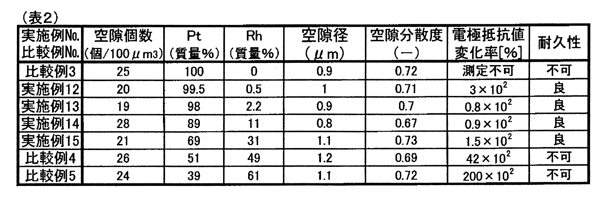
表2において、比較例3は、センサ素子1の検出面11から検出電極3、4が縮小しながら絶縁性基体の内部に向かって消失する。これにより、耐久試験後の電極抵抗値が測定不可となった。比較例3はPtにRhを配合していない。また、PtへのRhの配合比率の増加に伴い、電極抵抗変化率が上昇している。Rhの含有量が40質量%を超える比較例4、5は、耐久試験後の電極抵抗値が上昇し、充分な耐久性が得られていない。
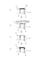
図15に示すように、PtにRhを配合していない比較例3では、(a)に示すPM検出後に、(b)の工程において、PtがPtO2となって揮散する。(b)の工程は、センサ素子1の検出面11に付着したPMを酸化除去するために、高温に加熱する工程である。そのため、(c)に示すPM除去の完了時に、検出電極3、4が縮小しながら検出面11から絶縁性基体の内部に向かって消失してしまう。(d)の工程において、再びPMを検出する際に、実際の電極間距離が初期状態より長くなる。この場合、図16に実線で示す初期状態の検出電流特性Aに対して、検出電流が規定値に達するまでの検出時間が、点線Bのように長くなる。これを繰り返すことで、さらに、検出時間が点線Cのように長くなり、規定時間tを超えてしまい、検出不可となる。
(実験例3)
実験例1と同様の方法で、センサ素子1を以下の条件下で作製し、実施例16~25とした。(1)PtとRhの粒状空隙5の個数が、19個/100μm3~28個/100μm3の範囲、(2)粒状空隙5の大きさが0.3μm~4.8μmの範囲、(3)空隙分散度が0.49~0.79の範囲。これら実施例16~25について、同様の耐久試験を行い、検出電極3、4の電極抵抗値の変化を測定した結果を、PtとRhの配合比率と共に、表3に示す。
実験例1と同様の方法で、センサ素子1を以下の条件下で作製し、実施例16~25とした。(1)PtとRhの粒状空隙5の個数が、19個/100μm3~28個/100μm3の範囲、(2)粒状空隙5の大きさが0.3μm~4.8μmの範囲、(3)空隙分散度が0.49~0.79の範囲。これら実施例16~25について、同様の耐久試験を行い、検出電極3、4の電極抵抗値の変化を測定した結果を、PtとRhの配合比率と共に、表3に示す。

表3において、粒状空隙5の大きさとRhの含有量が上記範囲にあるとき、空隙分散度が0.50を超える実施例16~25について、いずれも良好な耐久性が得られた。
(実験例4)
実験例1と同様の方法で、以下の条件下でセンサ素子1を作製し、実施例26~35とした。(1)PtとRhの粒状空隙5の個数が、19個/100μm3~28個/100μm3の範囲、(2)粒状空隙5の大きさが0.9μm~4.1μmの範囲、(3)空隙分散度が0.51~0.95の範囲。これら実施例26~36について、同様の耐久試験を行い、検出電極3、4の電極抵抗値の変化を測定した結果を、PtとRhの配合比率と共に、表4に示す。
実験例1と同様の方法で、以下の条件下でセンサ素子1を作製し、実施例26~35とした。(1)PtとRhの粒状空隙5の個数が、19個/100μm3~28個/100μm3の範囲、(2)粒状空隙5の大きさが0.9μm~4.1μmの範囲、(3)空隙分散度が0.51~0.95の範囲。これら実施例26~36について、同様の耐久試験を行い、検出電極3、4の電極抵抗値の変化を測定した結果を、PtとRhの配合比率と共に、表4に示す。
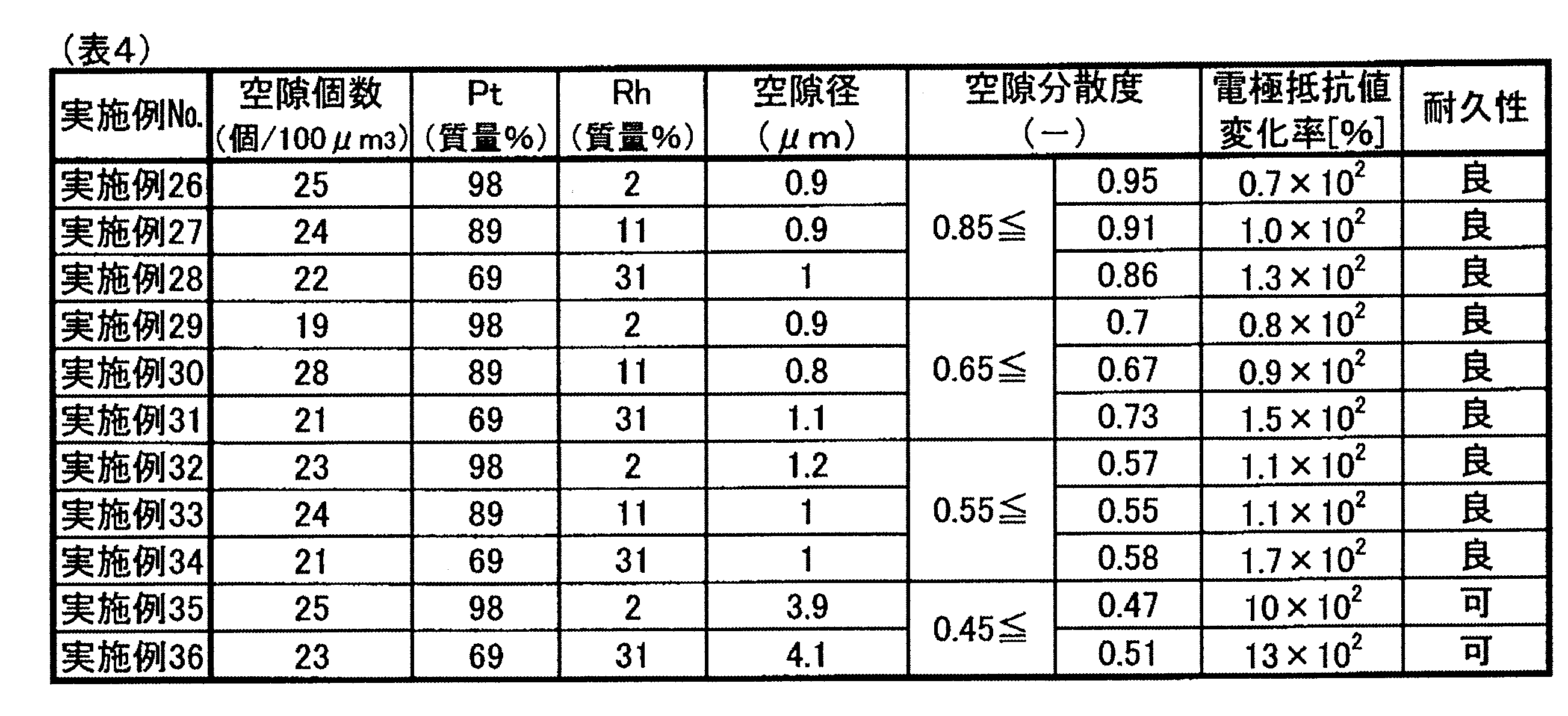
表4において、空隙分散度とRhの含有量が上記範囲にあるとき、粒状空隙5の大きさが3.9μm、4.1μmの実施例35、36については、やや電極抵抗変化率が大きくなった。その他の実施例26~34については、良好な耐久性が得られた。
(実験例5)
次に、検出電極3,4の電極材料として、PtとRhとの合金に代えて、Ptと、以下の金属との合金を用いた場合の、Ptの揮散に対する効果を調べた。上記金属とは、Rh、Ru、Ir、Os及びPdから少なくとも1種選ばれる金属である。検出電極3、4には、Ptとこれら金属との合金を、骨材と、電極ペーストを用い、実験例1と同様の方法でセンサ素子1を作製した。骨材はPt:各上記金属=98質量%:2質量%の配合比率とした合金粒子7と、アルミナからなる。電極ペーストは有機溶剤及び有機バインダを混合、混錬してなる。また、比較のため、Pt100質量%とした電極材料を用いて、同様の方法でセンサ素子1を作製した。
次に、検出電極3,4の電極材料として、PtとRhとの合金に代えて、Ptと、以下の金属との合金を用いた場合の、Ptの揮散に対する効果を調べた。上記金属とは、Rh、Ru、Ir、Os及びPdから少なくとも1種選ばれる金属である。検出電極3、4には、Ptとこれら金属との合金を、骨材と、電極ペーストを用い、実験例1と同様の方法でセンサ素子1を作製した。骨材はPt:各上記金属=98質量%:2質量%の配合比率とした合金粒子7と、アルミナからなる。電極ペーストは有機溶剤及び有機バインダを混合、混錬してなる。また、比較のため、Pt100質量%とした電極材料を用いて、同様の方法でセンサ素子1を作製した。
得られたセンサ素子1について、高温耐久試験を行った。まず、各センサ素子1を、温度900℃で250時間加熱した。その後、検出面11における検出電極3、4間の距離を測定し、高温耐久試験前の距離からの変化率を算出した。評価は、変化率が0%の場合を良、変化率が0%を超えかつ5%以下の場合を可と評価し、変化率が5%を超える場合を不可とした。
その結果、Pt100質量%のセンサ素子1は、変化率が5%を超え、不可と評価された。これに対して、Ptと、Rh、Ru、Ir又はOsとの合金を用いたセンサ素子1は、それぞれ変化率が0%であり、良好な結果が得られた。PtとPdとの合金を用いたセンサ素子1は、変化率が5%以下であり、他の金属よりもやや劣るものの、Ptの揮散を抑制する効果が見られた。
図18に示す対策前とは、従来のセンサ素子のことであり、その電極材料には樹脂ビーズが添加されていない。図18に示す対策後とは、対策前に対して、実験例1のように電極材料に樹脂ビーズを添加して作製したセンサ素子1のことである。また、対策前は上記試験例におけるPtとRhとの合金を用いたセンサ素子である。対策後のセンサ素子1の粒状空隙5の個数を、19個/100μm3~28個/100μm3の範囲に調整した。実験例1と同様に、耐久試験を行い、電極抵抗変化率を測定した。図17に示すように、従来素子と比較して、センサ素子1の電極内部に粒状空隙5が形成されていることが確認できた。その結果、粒状空隙5を形成した実施例37では、電極抵抗変化率が小さくなり、耐久性が向上した。
図18に示す、対策前のセンサ素子では、大気に露出する検出面の表面において、Rhの酸化により、金属酸化物が生成することが判明した。この金属酸化物の生成により、検出面の近傍においてRh濃度が低下する。検出電極の内部からRhが検出面に向けて拡散していく。これにより、さらにRhが酸化して、金属酸化物の偏析が生じる。そのため、検出面近傍の電極抵抗が増大し、全体としての電極抵抗値の上昇につながるものと推測される。
これに対して、図18に示す対策後のセンサ素子1では、電極内部にある粒状空隙5からの酸素供与により、検出面11のみならず、電極内部にも金属酸化物8が生成する。そのため、検出電極3、4の最表面と内部とで電極合金中のRh濃度差が低減して、Rhの電極最表面への拡散量が低下する。結果として、検出面11に露出する電極最表面の金属酸化物8の生成量が減少し、電極最表面部の抵抗値上昇率が低下する。これにより、検出電極3、4中のPtの揮散を抑制し、かつ、検出電極3、4の全体の抵抗値上昇率を低く抑えることができる。
本発明のセンサ素子用電極及びセンサ素子1は、上記実施形態、上記実施例に限定されるものではなく、本発明の趣旨を超えない範囲で、種々の変更が可能である。例えば、上記実施形態では、内燃機関の燃焼排ガスに含まれる粒子状物質を検出する、粒子状物質検出センサへの適用例について説明したが、粒子状物質が含まれる被測定ガスは、燃焼排ガスに限らず、また、DPF等の後処理装置の故障診断以外の用途に用いるものであってもよい。さらに、同様の検出電極構造を有し、粒子状物質以外の物質を検出するセンサ素子に適用することも、もちろんできる。
また、センサ素子1は、上記実施形態に記載したものに限らず、絶縁性基体2の表面に検出電極3、4の一部が露出する検出面11を有する構成であればよい。例えば、センサ素子1の絶縁性基体2や検出電極3、4の形状等は、適宜変更することができる。
1 センサ素子
11 検出面
2 絶縁性基体
3、4 検出電極
5 粒状空隙
7 合金粒子(すなわち、合金)
8 金属酸化物
11 検出面
2 絶縁性基体
3、4 検出電極
5 粒状空隙
7 合金粒子(すなわち、合金)
8 金属酸化物
Claims (8)
- 被測定ガス中の特定物質を検出するセンサ素子(1)用電極であって、
上記特定物質が付着する検出面(11)を有する絶縁性基体(2)に、上記検出面に一部が露出するように埋設されており、
Rh、Ru、Ir、Os及びPdからなるグループから選ばれる少なくとも1種の金属とPtとの合金(7)と、該合金間に分散配置された粒状空隙(5)と、を有し、
上記合金中の上記金属の含有量が40質量%以下であると共に、上記センサ素子用電極の単位体積あたりの上記粒状空隙の個数が、3個/100μm3~50個/100μm3である、センサ素子用電極。 - 上記金属はRhであり、上記合金中のRh含有量は、2質量%~30質量%である、請求項1に記載のセンサ素子用電極。
- 上記粒状空隙は、平均粒径が5μm以下である、請求項1又は2に記載のセンサ素子用電極。
- 上記特定物質は、粒子状物質である、請求項1~3のいずれか1項に記載のセンサ素子用電極。
- 被測定ガス中の特定物質を検出するセンサ素子(1)であって、
上記特定物質が付着する検出面(11)を有する絶縁性基体(2)と、
上記検出面に一部が露出して、残部が上記絶縁性基体に埋設される、互いに対向位置し、極性の異なる一対の検出電極(3、4)と、を備えており、
該検出電極は、Rh、Ru、Ir、Os及びPdからなるグループから選ばれる少なくとも1種の金属とPtとの合金(7)と、該合金間に分散配置された粒状空隙(5)と、を有し、
上記合金中の上記金属の含有量が40質量%以下であると共に、上記検出電極の単位体積あたりの上記粒状空隙の個数が、3個/100μm3~50個/100μm3である、センサ素子。 - 一対の上記検出電極は、それぞれ複数の電極(3a、4a)からなり、これら複数の電極は、交互に極性が異なるように、上記絶縁性基体の内部に間隔を置いて積層配設される、請求項5に記載のセンサ素子。
- 上記検出電極の積層方向(X)において、上記粒状空隙は、上記検出電極の中央部よりも両端部により多く配置される、請求項6に記載のセンサ素子。
- 上記検出電極の中央部と両端部に配置される上記粒状空隙の総個数に対して、上記検出電極の両端部に配置される上記粒状空隙の個数の比率である空隙分散度が、0.55~0.95の範囲にある、請求項7に記載のセンサ素子。
Priority Applications (3)
| Application Number | Priority Date | Filing Date | Title |
|---|---|---|---|
| DE112016005834.9T DE112016005834T5 (de) | 2015-12-17 | 2016-12-16 | Elektrode für sensorelement und sensorelement |
| CN201680073805.6A CN108369203B (zh) | 2015-12-17 | 2016-12-16 | 传感器元件 |
| US16/062,897 US10591431B2 (en) | 2015-12-17 | 2016-12-16 | Sensor element |
Applications Claiming Priority (2)
| Application Number | Priority Date | Filing Date | Title |
|---|---|---|---|
| JP2015-246409 | 2015-12-17 | ||
| JP2015246409A JP6406237B2 (ja) | 2015-12-17 | 2015-12-17 | センサ素子 |
Publications (1)
| Publication Number | Publication Date |
|---|---|
| WO2017104818A1 true WO2017104818A1 (ja) | 2017-06-22 |
Family
ID=59056732
Family Applications (1)
| Application Number | Title | Priority Date | Filing Date |
|---|---|---|---|
| PCT/JP2016/087597 Ceased WO2017104818A1 (ja) | 2015-12-17 | 2016-12-16 | センサ素子用電極及びセンサ素子 |
Country Status (5)
| Country | Link |
|---|---|
| US (1) | US10591431B2 (ja) |
| JP (1) | JP6406237B2 (ja) |
| CN (1) | CN108369203B (ja) |
| DE (1) | DE112016005834T5 (ja) |
| WO (1) | WO2017104818A1 (ja) |
Cited By (2)
| Publication number | Priority date | Publication date | Assignee | Title |
|---|---|---|---|---|
| WO2020045048A1 (ja) * | 2018-08-28 | 2020-03-05 | イビデン株式会社 | 粒子状物質検出センサ素子 |
| JP2020034349A (ja) * | 2018-08-28 | 2020-03-05 | イビデン株式会社 | 粒子状物質検出センサ素子 |
Families Citing this family (2)
| Publication number | Priority date | Publication date | Assignee | Title |
|---|---|---|---|---|
| US11513095B2 (en) | 2017-06-27 | 2022-11-29 | Kyocera Corporation | Sensor board and sensor device |
| US11353381B1 (en) * | 2020-06-09 | 2022-06-07 | Applied Materials, Inc. | Portable disc to measure chemical gas contaminants within semiconductor equipment and clean room |
Citations (3)
| Publication number | Priority date | Publication date | Assignee | Title |
|---|---|---|---|---|
| JP2012078130A (ja) * | 2010-09-30 | 2012-04-19 | Denso Corp | 粒子状物質検出センサおよびその製造方法 |
| JP2014066547A (ja) * | 2012-09-25 | 2014-04-17 | Tanaka Kikinzoku Kogyo Kk | センサー電極及びその製造方法、並びに、電極形成用の金属ペースト |
| JP2014145607A (ja) * | 2013-01-28 | 2014-08-14 | Tanaka Kikinzoku Kogyo Kk | ガスセンサー電極形成用の金属ペースト |
Family Cites Families (12)
| Publication number | Priority date | Publication date | Assignee | Title |
|---|---|---|---|---|
| DE2928496A1 (de) * | 1979-07-14 | 1981-01-29 | Bosch Gmbh Robert | Elektrochemischer messfuehler fuer die bestimmung des sauerstoffgehaltes in gasen |
| DE4408504A1 (de) * | 1994-03-14 | 1995-09-21 | Bosch Gmbh Robert | Sensor zur Bestimmung der Konzentration von Gaskomponenten in Gasgemischen |
| CN2754099Y (zh) * | 2004-12-01 | 2006-01-25 | 比亚迪股份有限公司 | 一种氧传感器 |
| CN101008630A (zh) * | 2006-01-23 | 2007-08-01 | 株式会社电装 | 用于气体传感器的气体检测元件及制造该元件的方法 |
| US20070245803A1 (en) * | 2006-02-23 | 2007-10-25 | Tan Siong S | Oxygen sensor with a protective layer |
| JP4996527B2 (ja) * | 2008-04-14 | 2012-08-08 | 日本特殊陶業株式会社 | 積層型ガスセンサ素子及びガスセンサ |
| DE102008041707A1 (de) | 2008-08-29 | 2010-03-04 | Robert Bosch Gmbh | Elektrode für einen resistiven Partikelsensor |
| JP5187417B2 (ja) * | 2010-09-10 | 2013-04-24 | 株式会社デンソー | ガスセンサ素子及びその製造方法 |
| US9304102B2 (en) * | 2012-03-08 | 2016-04-05 | Nextech Materials, Ltd. | Amperometric electrochemical sensors, sensor systems and detection methods |
| TWI499775B (zh) | 2013-01-28 | 2015-09-11 | Tanaka Precious Metal Ind | 氣體感測電極形成用之金屬膏 |
| JP6386805B2 (ja) | 2014-06-16 | 2018-09-05 | 株式会社Soken | 粒子状物質検出センサ素子及びこれを用いた粒子状物検出センサ |
| CN104049018A (zh) * | 2014-06-30 | 2014-09-17 | 东风电子科技股份有限公司 | NOx传感器芯片 |
-
2015
- 2015-12-17 JP JP2015246409A patent/JP6406237B2/ja active Active
-
2016
- 2016-12-16 WO PCT/JP2016/087597 patent/WO2017104818A1/ja not_active Ceased
- 2016-12-16 US US16/062,897 patent/US10591431B2/en active Active
- 2016-12-16 DE DE112016005834.9T patent/DE112016005834T5/de not_active Ceased
- 2016-12-16 CN CN201680073805.6A patent/CN108369203B/zh not_active Expired - Fee Related
Patent Citations (3)
| Publication number | Priority date | Publication date | Assignee | Title |
|---|---|---|---|---|
| JP2012078130A (ja) * | 2010-09-30 | 2012-04-19 | Denso Corp | 粒子状物質検出センサおよびその製造方法 |
| JP2014066547A (ja) * | 2012-09-25 | 2014-04-17 | Tanaka Kikinzoku Kogyo Kk | センサー電極及びその製造方法、並びに、電極形成用の金属ペースト |
| JP2014145607A (ja) * | 2013-01-28 | 2014-08-14 | Tanaka Kikinzoku Kogyo Kk | ガスセンサー電極形成用の金属ペースト |
Cited By (6)
| Publication number | Priority date | Publication date | Assignee | Title |
|---|---|---|---|---|
| WO2020045048A1 (ja) * | 2018-08-28 | 2020-03-05 | イビデン株式会社 | 粒子状物質検出センサ素子 |
| JP2020034349A (ja) * | 2018-08-28 | 2020-03-05 | イビデン株式会社 | 粒子状物質検出センサ素子 |
| JP2020034348A (ja) * | 2018-08-28 | 2020-03-05 | イビデン株式会社 | 粒子状物質検出センサ素子 |
| WO2020045049A1 (ja) * | 2018-08-28 | 2020-03-05 | イビデン株式会社 | 粒子状物質検出センサ素子 |
| CN112567234A (zh) * | 2018-08-28 | 2021-03-26 | 揖斐电株式会社 | 颗粒状物质检测传感器元件 |
| US11892422B2 (en) | 2018-08-28 | 2024-02-06 | Ibiden Co., Ltd. | Particulate-matter detecting sensor element |
Also Published As
| Publication number | Publication date |
|---|---|
| JP2017111036A (ja) | 2017-06-22 |
| CN108369203A (zh) | 2018-08-03 |
| US10591431B2 (en) | 2020-03-17 |
| US20190003997A1 (en) | 2019-01-03 |
| JP6406237B2 (ja) | 2018-10-17 |
| DE112016005834T5 (de) | 2018-08-30 |
| CN108369203B (zh) | 2020-10-16 |
Similar Documents
| Publication | Publication Date | Title |
|---|---|---|
| JP5542006B2 (ja) | 粒子状物質検出装置 | |
| JP5164896B2 (ja) | 粒子状物質検出装置 | |
| WO2017104818A1 (ja) | センサ素子用電極及びセンサ素子 | |
| JP5938133B1 (ja) | ガスセンサの検知電極、ガスセンサ、および、ガスセンサの製造方法 | |
| JP6536507B2 (ja) | 粒子状物質検出センサ | |
| CN110832315B (zh) | 气体传感器元件及气体传感器 | |
| JP5357347B1 (ja) | ガスセンサー電極形成用の金属ペースト | |
| JP6999455B2 (ja) | センサ素子及びガスセンサ | |
| JP6523144B2 (ja) | ガスセンサ | |
| WO2015105182A1 (ja) | 粒子状物質検出素子、粒子状物質検出センサ並びに粒子状物質検出素子の製造方法 | |
| JP2016008831A (ja) | NOxセンサ | |
| JP2017096909A (ja) | ガスセンサの検知電極、導電性ペーストの製造方法、ガスセンサ、および、ガスセンサの製造方法 | |
| JP5715549B2 (ja) | スクリーン印刷用電極ペースト及びそれを用いた電極の製造方法 | |
| JP5387550B2 (ja) | ガスセンサ素子の製造方法 | |
| JP6212328B2 (ja) | ガスセンサー電極形成用の金属ペースト | |
| JP2013530396A (ja) | 低コスト同時焼成センサ加熱回路 | |
| JP2018004652A (ja) | ガスセンサ | |
| JP6386805B2 (ja) | 粒子状物質検出センサ素子及びこれを用いた粒子状物検出センサ | |
| JP2022139228A (ja) | アンモニアセンサの検知電極形成用ペーストおよびガスセンサ素子の製造方法 | |
| JP6511304B2 (ja) | 粒子状物質検出センサ | |
| JP4780686B2 (ja) | ガスセンサ素子の製造方法及びガスセンサの製造方法 | |
| WO2016185841A1 (ja) | 粒子状物質検出センサ | |
| JP4426065B2 (ja) | ガスセンサ素子及びこれを備えるガスセンサ | |
| JP5892036B2 (ja) | ガスセンサ素子の製造方法 | |
| JP2003107034A (ja) | 積層型ガスセンサ素子及びこれを備えるガスセンサ |
Legal Events
| Date | Code | Title | Description |
|---|---|---|---|
| 121 | Ep: the epo has been informed by wipo that ep was designated in this application |
Ref document number: 16875792 Country of ref document: EP Kind code of ref document: A1 |
|
| WWE | Wipo information: entry into national phase |
Ref document number: 112016005834 Country of ref document: DE |
|
| 122 | Ep: pct application non-entry in european phase |
Ref document number: 16875792 Country of ref document: EP Kind code of ref document: A1 |