WO2017086196A1 - レジスト層付きマスクブランク、レジスト層付きマスクブランクの製造方法、及び、転写用マスクの製造方法 - Google Patents
レジスト層付きマスクブランク、レジスト層付きマスクブランクの製造方法、及び、転写用マスクの製造方法 Download PDFInfo
- Publication number
- WO2017086196A1 WO2017086196A1 PCT/JP2016/082927 JP2016082927W WO2017086196A1 WO 2017086196 A1 WO2017086196 A1 WO 2017086196A1 JP 2016082927 W JP2016082927 W JP 2016082927W WO 2017086196 A1 WO2017086196 A1 WO 2017086196A1
- Authority
- WO
- WIPO (PCT)
- Prior art keywords
- layer
- metal
- mask blank
- resist layer
- resist
- Prior art date
- Legal status (The legal status is an assumption and is not a legal conclusion. Google has not performed a legal analysis and makes no representation as to the accuracy of the status listed.)
- Ceased
Links
Images

Classifications
-
- G—PHYSICS
- G03—PHOTOGRAPHY; CINEMATOGRAPHY; ANALOGOUS TECHNIQUES USING WAVES OTHER THAN OPTICAL WAVES; ELECTROGRAPHY; HOLOGRAPHY
- G03F—PHOTOMECHANICAL PRODUCTION OF TEXTURED OR PATTERNED SURFACES, e.g. FOR PRINTING, FOR PROCESSING OF SEMICONDUCTOR DEVICES; MATERIALS THEREFOR; ORIGINALS THEREFOR; APPARATUS SPECIALLY ADAPTED THEREFOR
- G03F7/00—Photomechanical, e.g. photolithographic, production of textured or patterned surfaces, e.g. printing surfaces; Materials therefor, e.g. comprising photoresists; Apparatus specially adapted therefor
- G03F7/004—Photosensitive materials
- G03F7/09—Photosensitive materials characterised by structural details, e.g. supports, auxiliary layers
- G03F7/11—Photosensitive materials characterised by structural details, e.g. supports, auxiliary layers having cover layers or intermediate layers, e.g. subbing layers
-
- G—PHYSICS
- G03—PHOTOGRAPHY; CINEMATOGRAPHY; ANALOGOUS TECHNIQUES USING WAVES OTHER THAN OPTICAL WAVES; ELECTROGRAPHY; HOLOGRAPHY
- G03F—PHOTOMECHANICAL PRODUCTION OF TEXTURED OR PATTERNED SURFACES, e.g. FOR PRINTING, FOR PROCESSING OF SEMICONDUCTOR DEVICES; MATERIALS THEREFOR; ORIGINALS THEREFOR; APPARATUS SPECIALLY ADAPTED THEREFOR
- G03F1/00—Originals for photomechanical production of textured or patterned surfaces, e.g., masks, photo-masks, reticles; Mask blanks or pellicles therefor; Containers specially adapted therefor; Preparation thereof
- G03F1/38—Masks having auxiliary features, e.g. special coatings or marks for alignment or testing; Preparation thereof
- G03F1/40—Electrostatic discharge [ESD] related features, e.g. antistatic coatings or a conductive metal layer around the periphery of the mask substrate
-
- G—PHYSICS
- G03—PHOTOGRAPHY; CINEMATOGRAPHY; ANALOGOUS TECHNIQUES USING WAVES OTHER THAN OPTICAL WAVES; ELECTROGRAPHY; HOLOGRAPHY
- G03F—PHOTOMECHANICAL PRODUCTION OF TEXTURED OR PATTERNED SURFACES, e.g. FOR PRINTING, FOR PROCESSING OF SEMICONDUCTOR DEVICES; MATERIALS THEREFOR; ORIGINALS THEREFOR; APPARATUS SPECIALLY ADAPTED THEREFOR
- G03F1/00—Originals for photomechanical production of textured or patterned surfaces, e.g., masks, photo-masks, reticles; Mask blanks or pellicles therefor; Containers specially adapted therefor; Preparation thereof
- G03F1/38—Masks having auxiliary features, e.g. special coatings or marks for alignment or testing; Preparation thereof
-
- G—PHYSICS
- G03—PHOTOGRAPHY; CINEMATOGRAPHY; ANALOGOUS TECHNIQUES USING WAVES OTHER THAN OPTICAL WAVES; ELECTROGRAPHY; HOLOGRAPHY
- G03F—PHOTOMECHANICAL PRODUCTION OF TEXTURED OR PATTERNED SURFACES, e.g. FOR PRINTING, FOR PROCESSING OF SEMICONDUCTOR DEVICES; MATERIALS THEREFOR; ORIGINALS THEREFOR; APPARATUS SPECIALLY ADAPTED THEREFOR
- G03F1/00—Originals for photomechanical production of textured or patterned surfaces, e.g., masks, photo-masks, reticles; Mask blanks or pellicles therefor; Containers specially adapted therefor; Preparation thereof
- G03F1/68—Preparation processes not covered by groups G03F1/20 - G03F1/50
- G03F1/76—Patterning of masks by imaging
- G03F1/78—Patterning of masks by imaging by charged particle beam [CPB], e.g. electron beam patterning of masks
-
- G—PHYSICS
- G03—PHOTOGRAPHY; CINEMATOGRAPHY; ANALOGOUS TECHNIQUES USING WAVES OTHER THAN OPTICAL WAVES; ELECTROGRAPHY; HOLOGRAPHY
- G03F—PHOTOMECHANICAL PRODUCTION OF TEXTURED OR PATTERNED SURFACES, e.g. FOR PRINTING, FOR PROCESSING OF SEMICONDUCTOR DEVICES; MATERIALS THEREFOR; ORIGINALS THEREFOR; APPARATUS SPECIALLY ADAPTED THEREFOR
- G03F7/00—Photomechanical, e.g. photolithographic, production of textured or patterned surfaces, e.g. printing surfaces; Materials therefor, e.g. comprising photoresists; Apparatus specially adapted therefor
- G03F7/004—Photosensitive materials
- G03F7/039—Macromolecular compounds which are photodegradable, e.g. positive electron resists
-
- G—PHYSICS
- G03—PHOTOGRAPHY; CINEMATOGRAPHY; ANALOGOUS TECHNIQUES USING WAVES OTHER THAN OPTICAL WAVES; ELECTROGRAPHY; HOLOGRAPHY
- G03F—PHOTOMECHANICAL PRODUCTION OF TEXTURED OR PATTERNED SURFACES, e.g. FOR PRINTING, FOR PROCESSING OF SEMICONDUCTOR DEVICES; MATERIALS THEREFOR; ORIGINALS THEREFOR; APPARATUS SPECIALLY ADAPTED THEREFOR
- G03F1/00—Originals for photomechanical production of textured or patterned surfaces, e.g., masks, photo-masks, reticles; Mask blanks or pellicles therefor; Containers specially adapted therefor; Preparation thereof
- G03F1/26—Phase shift masks [PSM]; PSM blanks; Preparation thereof
Definitions
- the present invention relates to a mask blank with a resist layer, a method for manufacturing a mask blank with a resist layer, and a method for manufacturing a transfer mask.
- a resist layer is formed on a photomask blank in which an optical film (hereinafter also referred to as a “thin film”) such as a light shielding layer and a phase shift film is formed on a substrate, and the resist film is applied to the resist film. Then, electron beam irradiation is performed to form a resist pattern, and the resist pattern is further transferred to the light shielding layer and the phase shift film by etching.
- an optical film hereinafter also referred to as a “thin film”
- the resist film is applied to the resist film.
- electron beam irradiation is performed to form a resist pattern, and the resist pattern is further transferred to the light shielding layer and the phase shift film by etching.
- Patent Document 1 a technique for forming an organic conductive layer on the surface side of a resist layer is known (see, for example, Patent Document 1).
- the configuration in which the organic conductive layer is provided on the resist layer has an advantage that separation with a developer is possible by selecting a water-soluble material as the organic conductive layer.
- Patent Document 2 a technique for forming aluminum or a metal conductive film on the resist layer surface on the wafer substrate has been proposed (see, for example, Patent Document 2).
- JP 2014-9342 A Japanese Patent Laid-Open No. 63-288017
- the electrical resistance of the organic conductive layer is higher than that of the metal conductive layer, and the charge removal capability of the organic conductive layer is not sufficient.
- the metal conductive layer has low solubility in a solvent such as water solubility, so that peeling becomes difficult.
- an aluminum thin film has an insulator layer with a depth of about 2 to 5 nm formed on its surface by natural oxidation. For this reason, in the structure using an aluminum thin film, a static elimination capability is not fully obtained. Furthermore, there is a problem that the surface roughness of the aluminum thin film increases due to natural oxidation.
- an object of the present invention is to provide a mask blank with a resist layer capable of suppressing charge-up during electron beam irradiation, a method for manufacturing a mask blank with a resist layer, and the resist.
- the present invention provides a method for manufacturing a transfer mask using a mask blank with a layer.
- the present invention has the following configuration as means for solving the above-described problems.
- the thickness of the first metal layer is in the range of 5 nm to 15 nm
- the thickness of the second metal layer is in the range of 1 nm to 5 nm
- the thickness of the conductive layer is in the range of 7 nm to 20 nm.
- the mask blank with a resist layer in any one of 1-3.
- [Configuration 7] Preparing a substrate having a thin film; A resist layer forming step of forming a resist layer on the surface of the thin film; A conductive layer forming step of forming a conductive layer on the resist layer; The conductive layer forming step forms a first metal layer forming step of forming a first metal layer mainly composed of aluminum, and a second metal layer made of a metal other than aluminum is formed on the first metal layer.
- a method for producing a mask blank with a resist layer comprising: a second metal layer forming step.
- the method further includes a water-soluble resin layer forming step for forming a water-soluble resin layer on the resist layer, and the conductive layer forming step includes the water-soluble resin layer forming step.
- a method of manufacturing a transfer mask using the mask blank with a resist layer according to any one of configurations 1 to 6, A method for producing a transfer mask, comprising: a pattern forming step of forming an uneven pattern on at least a thin film of the mask blank with a resist layer.
- a mask blank with a resist layer capable of suppressing charge-up during electron beam irradiation, a method of manufacturing a mask blank with a resist layer, and transfer using the mask blank with a resist layer A method for manufacturing an industrial mask can be provided.
- FIG. 1 It is a section schematic diagram of a mask blank with a resist layer in this embodiment. It is the cross-sectional schematic of the modification of the mask blank with a resist layer. It is a cross-sectional schematic diagram which shows the manufacturing method of the mask blank with a resist layer shown in FIG.
- JP2013-257593A can be employed suitably.
- the contents of JP2013-257593A can be applied to the specific configuration of the thin film and the like.
- FIG. 1 is a schematic sectional view of a mask blank 10 with a resist layer in the present embodiment.
- the mask blank 10 with a resist layer has a configuration in which a thin film 12 is formed on the main surface of a substrate 11 and a resist layer 13 is formed on the thin film 12.
- a conductive layer 16 including a first metal layer 14 and a second metal layer 15 is formed on the resist layer 13.
- the expression “above” such as “on the resist layer” or “on the first metal layer” is only the configuration in which the target film is formed so as to be in contact with the main surface of each layer.
- a configuration in which another film is formed so as to be in contact with the main surface of each layer and then a target film is formed on the main surface of the other film is also included. Each configuration will be described below.
- a thin film-attached substrate (mask blank) 19 is composed of a substrate 11 and a thin film 12 comprising a light shielding layer 18 and a light semi-transmissive layer 17 provided on the substrate 11.
- the substrate 11 and the thin film 12 are the main body of the mask blank 19, and the mask blank 19 is provided as a transfer mask mainly by processing the thin film 12.
- a glass substrate As the substrate 11 in the mask blank 10 with a resist layer, a glass substrate can be used.
- a glass material having a high transmittance with respect to exposure light when forming a pattern on the wafer is selected for the substrate 11.
- a low thermal expansion glass that can minimize the thermal expansion of the substrate 11 accompanying the energy of exposure light is selected.
- the material of the substrate 11 is synthetic quartz glass, soda lime glass, aluminosilicate glass, borosilicate glass, non-alkali. Glass etc. are mentioned.
- a synthetic quartz glass having a high transmittance with respect to light with a wavelength of 300 nm or less is preferably used for the substrate 11 of a transfer mask that uses an ArF excimer laser with a wavelength of 193 nm or a KrF excimer laser with a wavelength of 254 nm as exposure light. be able to.
- the substrate 11 is more preferably within a range of about 0 ⁇ 1.0 ⁇ 10 ⁇ 7 / ° C. in order to suppress distortion of the transferred pattern due to heat during exposure.
- SiO 2 —TiO 2 glass which is a glass material having a low thermal expansion coefficient within the range of about 0 ⁇ 0.3 ⁇ 10 ⁇ 7 / ° C., can be preferably used.
- the mask blank 10 with a resist layer includes a thin film 12 on the main surface of the substrate 11 as shown in FIG.
- Specific configurations of the thin film 12 include the following (1) to (4). Note that when the first predetermined numerical value is represented by N1, the second predetermined numerical value is represented by N2, and N1 ⁇ N2, “N1 to N2” indicating the numerical range in the following description is the first predetermined numerical value. It means a range not less than N1 and not more than a second predetermined numerical value N2.
- the thin film 12 having the light shielding layer 18 is provided on the substrate 11 having transparency to the light of the exposure wavelength.
- the light shielding layer 18 is made of a material containing a transition metal alone or a compound thereof such as chromium, tantalum, ruthenium, tungsten, titanium, hafnium, molybdenum, nickel, vanadium, zirconium, niobium, palladium, rhodium.
- a transition metal alone or a compound thereof such as chromium, tantalum, ruthenium, tungsten, titanium, hafnium, molybdenum, nickel, vanadium, zirconium, niobium, palladium, rhodium.
- the light shielding layer 18 comprised with chromium and the chromium compound which added 1 or more types of elements chosen from elements, such as oxygen, nitrogen, and carbon, to chromium is mentioned.
- the light shielding layer 18 comprised with the tantalum compound which added 1 or more types of elements chosen from elements, such as oxygen, nitrogen, and boron, to tantalum is mentioned.
- the thin film 12 has a structure of the light shielding layer 18, a two-layer structure of the light shielding layer and the main surface antireflection layer, or a structure of three layers or more in which a back surface antireflection layer is added between the light shielding layer and the substrate 11. It is good. Moreover, it is good also as a composition gradient film
- the thin film 12 may have a configuration having an etching mask film on the light shielding layer 18.
- This etching mask film is made of chromium or a chromium compound obtained by adding an element such as oxygen, nitrogen, or carbon to chromium, having etching selectivity (etching resistance) with respect to etching of the light shielding layer 18 containing transition metal silicide. It is preferable to comprise.
- the transfer mask may be manufactured with the etching mask film remaining on the light shielding layer 18 by providing the etching mask film with an antireflection function.
- Thin film of binary mask having other configuration As another example of thin film 12 of binary mask, a light shielding layer made of a material containing a compound of transition metal and silicon (including transition metal silicide, particularly molybdenum silicide). A configuration having 18 can also be mentioned.
- the light shielding layer 18 is made of a material containing a transition metal and silicon compound. Examples of such a material include materials having transition metal and silicon as main components and oxygen and / or nitrogen.
- the light shielding layer 18 may be made of a material mainly composed of a transition metal and oxygen, nitrogen and / or boron.
- the transition metal molybdenum, tantalum, tungsten, titanium, hafnium, nickel, vanadium, zirconium, niobium, palladium, ruthenium, rhodium, chromium, and the like are applicable.
- the light shielding layer 18 is formed of a molybdenum silicide compound
- the light shielding layer (MoSi or the like) and the main surface antireflection layer (MoSiON or the like), or between the light shielding layer and the substrate 11 are used.
- a three-layer structure with a back-surface antireflection layer (MoSiON or the like) added can be formed.
- a thin film 12 having a light semi-transmissive layer 17 made of a material containing a compound of transition metal and silicon (including transition metal silicide, particularly molybdenum silicide) is provided.
- the light semi-transmissive layer 17 included in the thin film 12 transmits light having an intensity that does not substantially contribute to exposure (for example, 1% to 30% with respect to the exposure wavelength), and has a predetermined position with respect to the transmitted light.
- a phase difference (for example, 180 degrees) is given.
- the halftone phase shift mask has a light semi-transmission portion obtained by patterning the light semi-transmission layer 17 and a light transmission that transmits light having an intensity that contributes substantially to exposure without the light semi-transmission layer 17 formed. Part. And it is comprised so that the phase of the light which permeate
- the light passing through the vicinity of the boundary between the light semi-transmissive portion and the light transmissive portion and wrapping around the other region due to the diffraction phenomenon cancel each other.
- the light intensity at the boundary can be made almost zero, and the contrast of the boundary, that is, the resolution can be improved.
- the light semi-transmissive layer 17 is made of, for example, a material containing a compound of a transition metal and silicon (including a transition metal silicide), and includes a material having these transition metals and silicon and oxygen and / or nitrogen as main components. It is done.
- a transition metal molybdenum, tantalum, tungsten, titanium, hafnium, nickel, vanadium, zirconium, niobium, palladium, ruthenium, rhodium, chromium, or the like is applicable.
- the material of the light-semitransmissive layer 17 includes a transition metal and silicon. Therefore, a material having etching selectivity (having etching resistance) is preferable, and it is particularly preferable that the material is made of chromium or a chromium compound in which elements such as oxygen, nitrogen, and carbon are added to chromium.
- the thin film 12 is formed with a multilayer reflective film that reflects exposure light on the substrate 11, and the exposure light is irradiated on the multilayer reflective film.
- the absorber film to be absorbed has a structure formed in a pattern.
- Light incident on the reflective mask EUV light (extreme ultraviolet light having a wavelength of 13.5 nm)
- EUV light extreme ultraviolet light having a wavelength of 13.5 nm
- the optical image reflected by the multilayer reflective film is transferred onto the semiconductor substrate through the reflective optical system.
- the multilayer reflective film is formed by alternately laminating high refractive index layers and low refractive index layers.
- multilayer reflective films include Mo / Si periodic multilayer films, Ru / Si periodic multilayer films, Mo / Be periodic multilayer films, and Mo compound / Si compound periodic multilayer films in which Mo films and Si films are alternately stacked for about 40 periods. Examples include a film, a Si / Nb periodic multilayer film, a Si / Mo / Ru periodic multilayer film, a Si / Mo / Ru / Mo periodic multilayer film, and a Si / Ru / Mo / Ru periodic multilayer film.
- the material of the multilayer reflective film can be appropriately selected depending on the exposure wavelength.
- the absorber film has a function of absorbing exposure light such as EUV light, and for example, tantalum (Ta) alone or a material mainly composed of Ta can be preferably used.
- the crystalline state of such an absorber film preferably has an amorphous or microcrystalline structure from the viewpoint of smoothness and flatness.
- the resist layer 13 can be formed by a known method using a conventionally known resist composition.
- a conventionally known resist composition For example, known positive resists, negative resists, and chemically amplified resists can be used.
- the resist composition may contain a photosensitive resin, a photoacid generator (PAG), a basic compound, a surfactant, and an organic solvent as a solvent.
- PAG photoacid generator
- the conductive layer 16 includes a first metal layer 14 mainly composed of aluminum and a second metal layer 15 composed of a metal other than aluminum.
- the conductive layer 16 has a configuration in which a first metal layer 14 is provided on the resist layer 13 side, and a second metal layer 15 is provided on the first metal layer 14. . Thereby, it is set as the structure which the 1st metal layer 14 which has aluminum as a main component is not exposed in the surface of the mask blank 10 with a resist layer.
- the total thickness of the conductive layer 16 is preferably 7 nm to 20 nm.
- the reason is as follows. This is because if the thickness of the conductive layer 16 is less than 7 nm, it is difficult to ensure sufficient conductivity for suppressing charge-up caused by electron beam irradiation. If the thickness of the conductive layer 16 is more than 20 nm, a residue is easily generated when the conductive layer 16 is removed in the process of manufacturing the transfer mask using the mask blank 10 with a resist layer, and remains as a foreign matter. This is because the possibility increases.
- the conductive layer 16 has a sheet resistance of 10 ⁇ / sq. To 1.0 ⁇ 10 6 ⁇ / sq. And preferably 100 ⁇ / sq. To 1.0 ⁇ 10 5 ⁇ / sq. It is more preferable that The sheet resistance is a value measured by a four-probe method defined in JIS K 7194: 1994. The reason is as follows.
- the sheet resistance of the conductive layer 16 is 1.0 ⁇ 10 6 ⁇ / sq. This is because the static elimination effect is insufficient and the pattern position accuracy deteriorates.
- the sheet resistance of the conductive layer 16 is 10 ⁇ / sq. This is because if the value is less than 1, the electrons flowing through the conductive film 16 may affect the resist film, which may reduce the sensitivity.
- the conductive layer 16 preferably has a surface roughness Ra of 2 nm or less.
- the roughness is a value measured by a method defined in JIS B 0601: 2001.
- the first metal layer 14 is composed mainly of aluminum.
- the main component means a component having the highest ratio in the structure, and in the first metal layer 14, it means that aluminum is a component having the highest composition ratio (atomic ratio).
- the atomic composition percentage of aluminum is preferably 80 at% or more, and more preferably 90 at% or more as the content (content).
- the first metal layer 14 is made of aluminum except for inevitable impurities.
- Aluminum is alkali-soluble. Therefore, aluminum can be easily removed by pre-rinsing with pure water (ion exchange water) or an alkaline solution before development or an alkaline developer. For this reason, a transfer mask can be manufactured from a mask blank, without adding the process for peeling the 1st metal layer 14.
- FIG. 1 is alkali-soluble. Therefore, aluminum can be easily removed by pre-rinsing with pure water (ion exchange water) or an alkaline solution before development or an alkaline developer. For this reason, a transfer mask can be manufactured from a mask blank, without adding the process for peeling the 1st metal layer 14.
- the thickness of the first metal layer 14 is preferably 5 nm to 15 nm, and preferably 7 nm to 10 nm. The reason is as follows. This is because if the thickness of the first metal layer 14 is less than 5 nm, it is difficult to ensure sufficient conductivity for suppressing charge-up by electron beam irradiation. On the other hand, if the thickness of the first metal layer 14 is more than 15 nm, aluminum is removed when the conductive layer 16 and the first metal layer 14 are removed in the step of producing a transfer mask using the mask blank 10 with a resist layer. This is because such a residue is likely to be generated and the possibility of remaining as a foreign substance increases.
- the first metal layer 14 has a sheet resistance of 1.0 ⁇ 10 6 ⁇ / sq. To 5.0 ⁇ / sq. It is preferable that it is the range of these. The reason is as follows.
- the sheet resistance of the first metal layer 14 is 5.0 ⁇ / sq. If lower than that, electrons spread from the electron beam irradiation position to the peripheral portion through the first metal layer 14, and the shape of the resist pattern may be deteriorated.
- the sheet resistance of the first metal layer 14 is 1.0 ⁇ 10 5 ⁇ / sq. If it is higher than the range, there is a possibility that the charge eliminating effect may be poor.
- the first metal layer 14 is measured by using an atomic force microscope (AFM) as a surface roughness, and when Ra (center line surface roughness) is obtained based on height data in a 10 nm square range,
- the surface roughness Ra is preferably 0.7 nm or less. The reason is as follows. When the surface roughness Ra of the first metal layer 14 exceeds 0.7 nm, the surface area of the first metal layer 14 increases, and oxidation occurs at the interface between the first metal layer 14 and the second metal layer 15. This is because it has a problem that it tends to occur.
- the second metal layer 15 is made of a metal other than aluminum.
- the second metal layer 15 made of a metal other than aluminum is substantially free of aluminum.
- “substantially does not contain aluminum” is a configuration that does not contain aluminum except for inevitable impurities and diffusion from the first metal layer 14, and specifically, the content (content ratio) It means that the atomic composition percentage of aluminum is less than 1 at%.
- the metal other than aluminum it is preferable to use a material that can be formed in a state where the same vacuum is maintained from the formation of the aluminum film of the first metal layer 14.
- the metal other than aluminum it is preferable to use a material capable of forming a highly dense film and capable of being formed by sputtering.
- the first metal layer 14 is in an airtight state and, for example, the first metal layer 14 is not deteriorated due to oxygen or the like present in the atmosphere during storage. It becomes. That is, the second metal layer 15 functions as a protective layer for the first metal layer 14. For this reason, the oxidation of the aluminum which comprises the 1st metal layer 14 by the 2nd metal layer 15 is suppressed. Furthermore, since the second metal layer 15 does not substantially contain aluminum, an increase in sheet resistance and an increase in surface roughness due to oxidation of aluminum can be suppressed.
- a metal oxide may be formed on the surface of the second metal layer 15 by natural oxidation.
- a metal other than a noble metal is used as the second metal layer 15
- an oxide film of a metal constituting the second metal layer 15 is formed on the surface (that is, the exposed surface) of the mask blank 10 with a resist film. Is done.
- “formation of a metal oxide film” means a structure in which a metal oxide film constituting the second metal layer 15 is formed on the surface of the second metal layer 15, or the first A configuration in which all the metals constituting the two-metal layer 15 are oxidized is also included.
- the metal constituting the second metal layer 15 is preferably a transition metal.
- the reason is as follows. This is because even if the transition metal is a metal having a low standard electrode potential, the natural oxidation does not increase the oxidation number enough to become an insulator, and the conductivity is maintained. For example, oxides of Mo (III, IV) and W (IV) have good conductivity. For this reason, when the second metal layer 15 is formed of a transition metal, conductivity is ensured even if the surface of the second metal layer 15 is oxidized, and charge-up due to electron beam irradiation can be suppressed.
- the metal constituting the second metal layer 15 preferably has a higher oxidation-reduction potential than aluminum.
- the reason is as follows. Since the redox potential of the metal constituting the second metal layer 15 is higher than that of aluminum, the metal constituting the second metal layer 15 is more easily oxidized than the aluminum constituting the first metal layer 14. Because. For this reason, when the 2nd metal layer 15 becomes a sacrificial layer of oxidation, it can suppress that the aluminum which comprises the 1st metal layer 14 oxidizes.
- the conductivity required for the conductive layer 16 can be maintained if the aluminum constituting the first metal layer 14 is not oxidized. Specifically, since the aluminum constituting the first metal layer 14 has very high conductivity, even when the resistance of the second metal layer 15 is higher than that of the first metal layer 14, the conductivity of the entire conductive layer 16 is increased. Sex is secured by aluminum. Therefore, the conductivity of the conductive layer 16 can be sufficiently ensured.
- the aluminum constituting the first metal layer 14 is oxidized, it becomes difficult to sufficiently secure the conductivity of the conductive layer 16, and the sheet resistance of the first metal layer 14 increases. For this reason, it is disadvantageous to suppress charge-up due to electron beam irradiation. Furthermore, when aluminum is oxidized, the surface roughness of the first metal layer 14 increases, which is disadvantageous in terms of the quality of the mask blank described later.
- the conductive layer 16 preferably has a highly smooth layer formed on the surface. The reason is as follows. This is because if the roughness of the surface of the conductive layer 16 is large, the thickness may not be measured in the inspection as a mask blank. For this reason, the conductive layer 16 is required to be smooth enough to be inspected as a mask blank.
- the thickness of the conductive layer may not be inspected, and there may be a problem in the quality as the mask blank.
- the surface roughness of the second metal layer 15 is defined in the same manner as the surface roughness of the conductive layer 16, the surface roughness Ra is preferably 0.7 nm or less. In the case where the second metal layer 15 is formed on the surface of the conductive layer 16, the roughness of the second metal layer 15 is the roughness of the conductive layer 16.
- the thickness of the conductive layer 16 depends on the surface shape of the other layer. For this reason, when a layer other than the second metal layer 15 is formed on the surface of the conductive layer 16, the surface roughness of the second metal layer 15 is not particularly limited. However, also in this configuration, the smoother the surface of the second metal layer 15, the easier the surface of this upper layer becomes. Therefore, it is preferable that the second metal layer 15 is also formed smoothly.
- the second metal layer 15 is preferably formed of a metal having a melting point higher than that of aluminum.
- a metal having a melting point higher than that of aluminum is deposited on the substrate as finer particles rather than clusters during film formation by sputtering or the like. For this reason, it is difficult for metal agglomerates to occur on the film formation surface, and a film having a uniform thickness in the surface direction is more easily formed than the first metal layer 14 made of aluminum.
- the second metal layer 15 made of a metal having a melting point higher than that of aluminum on the first metal layer 14 made of aluminum
- the unevenness on the surface of the first metal layer 14 made of aluminum can be made uneven.
- the second metal layer 15 can be smoothed.
- the second metal layer 15 can be used without any particular limitation as long as it is a metal material that functions as a protective layer for the first metal layer 14 mainly composed of aluminum.
- the second metal layer 15 preferably includes one or more metals selected from elements included in the range from the fourth group element to the sixth group element.
- the second metal layer 15 is preferably composed of molybdenum, tungsten, tantalum, and niobium.
- the second metal layer 15 with molybdenum.
- the second metal layer 15 By forming the second metal layer 15 using these materials, it is possible to prevent oxidation of aluminum constituting the first metal layer 14 and improve the smoothness of the surface of the conductive layer 16. Become.
- the thickness of the second metal layer 15 is preferably 1 nm to 5 nm. The reason is as follows. This is because if the thickness of the second metal layer 15 is less than 1 nm, both the suppression of oxidation of the first metal layer 14 and the smoothing of the surface of the conductive layer 16 may be insufficient. Further, if the thickness of the second metal layer 15 is more than 5 nm, a residue of the conductive layer 16 is likely to be generated when the conductive layer 16 is removed. Moreover, it is because it will become disadvantageous for formation of the fine pattern of a mask blank if the thickness of the electroconductive layer 16 is too thick than 5 nm.
- a metal oxide formed by natural oxidation is formed on the surface of the second metal layer 15.
- the second metal layer 15 is made of a metal such as molybdenum, tungsten, titanium, and chromium, the oxide has conductivity, and the portion other than the natural oxide film on the surface is oxidized. The state of not metal is maintained. Therefore, even if the thickness of the second metal layer 15 is 5 nm or less, the conductive layer 16 can maintain sufficient conductivity.
- the first metal layer 14 made of aluminum is provided on the resist layer 13, and the second metal layer made of metal other than aluminum is formed on the first metal layer 14. 15 is provided. Since aluminum applied to the first metal layer 14 has high conductivity, even if the second metal layer 15 is formed thin, the conductive layer 16 can obtain sufficient conductivity. For example, even if the second metal layer 15 is a layer of 5 nm or less, the conductivity of the conductive layer 16 is sufficiently ensured. For this reason, even when the second metal layer 15 is a thin layer, it is possible to effectively neutralize the charging of the resist layer 13 that occurs during electron beam irradiation. As a result, it is possible to suppress charge-up due to electron beam irradiation.
- the first metal layer 14 includes a layer containing aluminum as a main component, the first metal layer 14 can be used as compared with the case where an organic conductive layer as in Patent Document 1 is used as a conductive layer for suppressing charge-up.
- the conductive layer 16 of the embodiment can be formed thin. For this reason, compared with the case where the organic electroconductive layer etc. are formed on the resist layer like the said patent document 1, the electroconductive layer 16 of this embodiment tends to give a fine pattern favorably to a mask blank. Thus, the conductivity at the time of pattern drawing by electron beam irradiation can be dramatically improved.
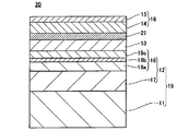
- FIG. 2 is a schematic sectional view of a modification of the mask blank with a resist layer.
- a mask blank 20 with a resist layer shown in FIG. 2 has a configuration in which a thin film 12 is formed on the main surface of a substrate 11 and a resist layer 13 is formed on the thin film 12. Further, in the mask blank 20 with a resist layer, a water-soluble resin layer 21 is formed on the resist layer 13, and the conductive layer 16 including the first metal layer 14 and the second metal layer 15 is formed on the water-soluble resin layer 21. Is formed.
- the mask blank 20 with a resist layer has the same configuration as the mask blank 10 with a resist layer shown in FIG. 1 except that the water-soluble resin layer 21 is formed. Therefore, in the following description, only the configuration related to the water-soluble resin layer 21 will be described, and detailed description of the configuration similar to the mask blank 10 with a resist layer shown in FIG. 1 will be omitted.
- the water-soluble resin layer 21 is formed on the main surface of the resist layer 13.
- the water-soluble resin layer 21 has water solubility. Thereby, the removability of the conductive layer 16 formed on the water-soluble resin layer 21 can be enhanced by pre-rinsing or development using water or an alkaline solution.
- water-soluble resin layer 21 examples include polyvinyl alcohol (PVA), polyvinyl pyrrolidone (PVP), polyacrylic acid polymer, polyacrylamide (PAM), polyethylene oxide (PEO), and polyaniline which is a conductive polymer.
- PVA polyvinyl alcohol
- PVP polyvinyl pyrrolidone
- PAM polyacrylamide
- PEO polyethylene oxide
- polyaniline which is a conductive polymer.
- the water-soluble resin layer 21 is preferably formed so as to cover the main surface of the resist layer 13, and is preferably formed so as to cover the side surface of the resist layer 13.
- the conductive layer 16 is preferably formed so as to cover the main surface of the water-soluble resin layer 21 and the side surfaces of the water-soluble resin layer 21.
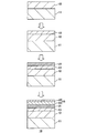
- FIG. 3 is a schematic cross-sectional view showing a method for manufacturing the mask blank 20 with a resist layer shown in FIG.
- the step of forming the water-soluble resin layer 21 described later is not performed.
- the mask blank 10 with a resist layer configured as shown in FIG. 1 can be manufactured in the same manner as the mask blank 20 with a resist layer shown in FIG. 2 except for the step of forming the water-soluble resin layer 21.
- the substrate 11 is prepared and the thin film 12 is formed on the substrate 11 is shown.
- the thin film 12 is formed on the substrate 11 in advance.
- the mask blank 19 may be prepared, and the resist layer 13 may be formed on the prepared mask blank 19.
- a resist layer 13 is formed on the main surface of the thin film 12 formed on the substrate 11 using a positive resist solution.
- a positive resist solution As a specific method, a known method can be used. For example, a resist solution is applied to the main surface of the thin film 12 by spin coating, and a baking process is performed. Thereby, the resist layer 13 covering the thin film 12 can be formed.
- a water-soluble resin layer 21 is formed on the main surface of the resist layer 13 using an organic conductive polymer.
- an organic conductive polymer As a specific method, a known method can be used. For example, a water-soluble resin raw material liquid is applied to the main surface of the resist layer 13 by spin coating. Then, rough drying is performed to form a water-soluble resin layer 21 so as to cover the resist layer 13. In the case where the water-soluble resin layer 21 is not provided as in the mask blank 10 with a resist layer shown in FIG. 1, this water-soluble resin layer forming step may not be performed.
- the conductive layer 16 is formed on the main surface of the water-soluble resin layer 21.
- the first metal layer 14 made of aluminum is first formed, the first metal layer 14 is formed, and then the second metal layer 15 made of a metal other than aluminum is formed.
- an aluminum oxide film is not formed on the surface of the first metal layer 14 during the period from the end of the formation of the first metal layer 14 to the start of the formation of the second metal layer 15.
- the first metal layer 14 and the second metal layer 15 are preferably formed continuously without exposure to the air or exposure to an oxygen gas atmosphere.
- the first metal layer 14 made of aluminum can be formed using a known method.
- the first metal layer 14 may be formed by, for example, sputtering film formation, or may be formed by vacuum deposition.
- the second metal layer 15 made of a metal other than aluminum can be formed by a known method using the above-described metal material.
- the second metal layer 15 may be formed by, for example, sputtering film formation, or may be formed by vacuum deposition. Both the first metal layer 14 and the second metal layer 15 are preferably formed using ion beam sputtering.
- the mask blank 20 with a resist layer can be produced.
- a cleaning / drying step and the like necessary for producing a mask blank with a resist layer can be appropriately performed.
- a transfer mask can also be produced from the mask blank with a resist layer of the above-described embodiment.
- the transfer mask includes at least a thin film in which a predetermined uneven pattern is formed in the above-described mask blank.
- the transfer mask can be produced by the following method.
- the above-described mask blank with a resist layer is subjected to exposure (drawing) by electron beam irradiation corresponding to a predetermined pattern, and then a pattern forming step of forming a resist pattern by development is performed.
- a known method may be used as a specific method for static elimination.
- a thin film having a predetermined uneven pattern is produced.
- the pattern formation process here may point out forming a resist pattern, and also may form an uneven
- Example 1 With reference to FIG. 1, the manufacturing method of the mask blank 10 with a resist layer concerning Example 1 is demonstrated.
- [Manufacture of mask blank 10 with resist layer] (Preparation of substrate with thin film) First, a synthetic quartz glass substrate having a size of 6 inches square and a thickness of 0.25 inches was prepared as the translucent substrate 11.
- the light semi-transmissive layer 17 was produced on the prepared translucent substrate 11 by the following method.
- Reactive sputtering (DC sputtering) was performed at 0 kW.
- a MoSiN film made of molybdenum, silicon and nitrogen was formed to a thickness of 69 nm.
- the substrate on which the MoSiN film was formed was subjected to a heat treatment in the atmosphere using a heating furnace at a heating temperature of 450 ° C. and a heating time of 1 hour, so that a light semi-transmissive layer 17 was produced.
- This MoSiN film had an transmittance of 6.16% and a phase difference of 184.4 degrees in an ArF excimer laser.
- a light shielding layer 18 was formed on the light semi-transmissive layer 17 by the following method.
- a CrOCN film 18a having a thickness of 30 nm was formed.
- Sputtering DC sputtering was performed to form a 4 nm thick CrN film 18b.
- a chromium-based light shielding layer 18 having a three-layer structure having a total film thickness of 48 nm was produced.
- a chemically amplified positive resist (PRL009S manufactured by FUJIFILM Electromaterial Co., Ltd.) is applied to the surface of the thin film 12 produced by the above-described method by a spin coating method, and a baking process (prebaking) is performed at 140 ° C. for 600 seconds to obtain a film thickness of 120 nm.
- the resist layer 13 was formed.
- a first metal layer 14 made of aluminum with a thickness of 7 nm was formed on the resist layer 13 after the baking (pre-baking) by ion beam sputtering using an aluminum target. Further, a second metal layer 15 made of molybdenum with a thickness of 3 nm was formed on the first metal layer 14 by ion beam sputtering using a molybdenum target.
- the surface sheet resistance composed of the first metal layer 14 and the second metal layer 15 is about 50 ⁇ 10 2 ⁇ / sq.
- the conductive layer 16 was prepared. Moreover, the mask blank 10 with the resist layer of Example 1 provided with the resist layer 13 and the electroconductive layer 16 on the board
- Example 2 With reference to FIG. 2, the manufacturing method of the mask blank 20 with a resist layer concerning Example 2 is demonstrated.
- the water-soluble resin layer 21 was formed by the following method.
- the conductive layer 16 was produced in the same manner as in Example 1 except that the thickness of the first metal layer 14 made of aluminum formed on the water-soluble resin layer 21 was 6 nm.
- the mask blank 20 with a resist layer of Example 2 provided with the resist layer 13, the water-soluble resin layer 21, and the electroconductive layer 16 on the board
- a polyaniline-based organic conductive resin film (AQUA SAVE manufactured by Mitsubishi Rayon Co., Ltd.) is applied on the resist layer 13 after the baking process (pre-baking) by spin coating, and roughly dried at 70 ° C. From the organic conductive resin The sheet resistance is approximately 10 ⁇ 10 8 ⁇ / sq. A water-soluble resin layer 21 having a thickness of 10 nm was formed.
- a first metal layer made of aluminum was formed with a thickness of 10 nm by an ion beam sputtering method using an aluminum target, and a conductive layer made only of the first metal layer was produced. .
- Example 1 and Example 2 pre-rinsing was performed and the electroconductive layer 16 was removed with the pure water (ion-exchange water) or the alkaline solution. Subsequent development was performed. Development was performed by supplying a developer (THAM: tetramethylammonium hydroxide) to the substrate at 5 mL / second. Then, drying rotation for 60 seconds was performed at high speed rotation, and it was made to dry naturally. In addition, the process after the removal of a resist pattern was not performed.
- THAM tetramethylammonium hydroxide
- Example 1 and Example 2 When the obtained resist pattern was observed with an electron microscope, in Example 1 and Example 2, it was possible to form a pattern at a predetermined position satisfactorily at a half pitch of the size. From this, in Example 1 and Example 2, it turned out that the charge at the time of resist pattern formation was eliminated rapidly.
- Comparative Example 1 there was a phenomenon in which the position of the actually formed pattern was shifted from the predetermined position to be drawn when the half pitch was smaller than 70 nm. Further, when the surface state of the conductive layer was confirmed, an aluminum oxide layer was formed on the surface, and the surface roughness was increased.
Landscapes
- Physics & Mathematics (AREA)
- General Physics & Mathematics (AREA)
- Engineering & Computer Science (AREA)
- Plasma & Fusion (AREA)
- Spectroscopy & Molecular Physics (AREA)
- Architecture (AREA)
- Structural Engineering (AREA)
- Preparing Plates And Mask In Photomechanical Process (AREA)
- Materials For Photolithography (AREA)
- Exposure And Positioning Against Photoresist Photosensitive Materials (AREA)
Abstract
Description
また、ウエハ基板上のレジスト層表面にアルミニウムや金属導電膜を形成する技術も提案されている(例えば、特許文献2参照)。
また、金属導電性層の溶解性を考慮すると、アルカリ性の現像液に溶解可能なアルミニウムを用いることが考えられる。しかしながら、アルミニウム薄膜は、その表面に自然酸化による深さ2~5nm程度の絶縁体層が形成されてしまう。このため、アルミニウム薄膜を用いる構成では、除電能力が充分に得られない。さらに、自然酸化により、アルミニウム薄膜の表面粗さが増してしまう問題もある。
薄膜を有する基板と、
前記薄膜の表面に形成されたレジスト層と、
前記レジスト層上に形成された導電性層と、を備え、
前記導電性層が、アルミニウムを主成分とする第1金属層と、アルミニウム以外の金属からなる第2金属層とを有し、
前記第1金属層が、前記第2金属層よりもレジスト層側に設けられている
レジスト層付きマスクブランク。
前記第2金属層が、アルミニウムよりも酸化還元電位の高い金属からなる構成1に記載のレジスト層付きマスクブランク。
[構成3]
前記第2金属層が、モリブデン、タングステン、チタン、及び、クロムから選ばれる1種以上を含む構成1又は2に記載のレジスト層付きマスクブランク。
前記第1金属層の厚さが5nm~15nmの範囲にあり、前記第2金属層の厚さが1nm~5nmの範囲にあり、前記導電性層の厚さが7nm~20nmの範囲にある構成1から3のいずれかに記載のレジスト層付きマスクブランク。
前記導電性層と前記レジスト層との間に形成された、水溶性樹脂層を更に備える構成1から4のいずれかに記載のレジスト層付きマスクブランク。
前記水溶性樹脂層が、有機導電性ポリマーからなる有機導電性層である構成5に記載のレジスト層付きマスクブランク。
薄膜を有する基板を準備する工程と、
前記薄膜の表面にレジスト層を形成するレジスト層形成工程と、
前記レジスト層上に、導電性層を形成する導電性層形成工程と、を有し、
前記導電性層形成工程が、アルミニウムを主成分とする第1金属層を形成する第1金属層形成工程と、前記第1金属層上に、アルミニウム以外の金属からなる第2金属層を形成する第2金属層形成工程と、を含む
レジスト層付きマスクブランクの製造方法。
前記レジスト層形成工程と前記導電性層形成工程との間に、前記レジスト層上に水溶性樹脂層を形成する水溶性樹脂層形成工程を更に有し、前記導電性層形成工程は、前記水溶性樹脂層上に前記導電性層を形成する構成7に記載のレジスト層付きマスクブランクの製造方法。
構成1~6のいずれかに記載のレジスト層付きマスクブランクを用いる転写用マスクの製造方法であって、
前記レジスト層付きマスクブランクの少なくとも薄膜に、凹凸パターンを形成するパターン形成工程を有する
転写用マスクの製造方法。
本実施形態においては、次の順序で説明を行う。
1.レジスト層付きマスクブランク
(1-A)薄膜付基板
(1-B)レジスト層
(1-C)導電性層
(1-D)水溶性樹脂層(有機導電性層)
2.レジスト層付きマスクブランクの製造方法
(2-A)薄膜付基板(マスクブランク)準備工程
(2-B)レジスト層形成工程
(2-C)水溶性樹脂層(有機導電性層)形成工程
(2-D)導電性層形成工程
3.転写用マスクの製造方法
図1は、本実施形態におけるレジスト層付きマスクブランク10の断面概略図である。図1に示すように、レジスト層付きマスクブランク10は、基板11の主表面に薄膜12が形成され、薄膜12の上にレジスト層13が形成された構成を有する。さらに、レジスト層付きマスクブランク10では、レジスト層13上に、第1金属層14と第2金属層15とからなる導電性層16が形成されている。
薄膜付き基板(マスクブランク)19は、基板11と、この基板11上に設けられた遮光層18や光半透過層17等からなる薄膜12とから構成されている。この基板11と薄膜12とがマスクブランク19の主体であり、主に薄膜12が加工されることによりマスクブランク19が転写用マスクとして供される。
また、反射型マスクであるEUVマスクの場合、基板11には、露光時の熱による被転写パターンの歪みを抑えるために、約0±1.0×10⁻⁷/℃の範囲内、より好ましくは約0±0.3×10-7/℃の範囲内の低熱膨張係数を有するガラス材料であるSiO2-TiO2系ガラスを好ましく用いることができる。
また、バイナリマスクの薄膜12の他の例としては、遷移金属及びケイ素(遷移金属シリサイド、特にモリブデンシリサイドを含む)の化合物を含む材料からなる遮光層18を有する構成も挙げることができる。
また、遮光層18の膜厚方向における組成が連続的又は段階的に異なる組成傾斜膜としてもよい。
レジスト層付きマスクブランク10がハーフトーン型位相シフトマスクである場合には、転写時に使用する露光光の波長に対して透過性を有する基板11上に、遷移金属及びケイ素(遷移金属シリサイド、特にモリブデンシリサイドを含む)の化合物を含む材料からなる光半透過層17を有する薄膜12が設けられる。
レジスト層付きマスクブランク10が反射型マスクである場合、薄膜12は、基板11上に露光光を反射する多層反射膜が形成され、多層反射膜上に露光光を吸収する吸収体膜がパターン状に形成された構造を有する。反射型マスクに入射した光(EUV光(波長13.5nmの極端紫外線))は、吸収体膜のある部分では吸収される。また、吸収体膜のない部分では、多層反射膜で反射された光像が、反射光学系を通して半導体基板上に転写される。
レジスト層13は、従来公知のレジスト組成物を用いて、公知の手法で形成することができる。例えば、公知のポジ型のレジスト、ネガ型のレジスト、及び、化学増幅型レジストを使用することができる。また、レジスト組成物としては、感光性樹脂、光酸発生剤(PAG)、塩基性化合物、界面活性剤、及び、溶媒である有機溶剤等が含まれていてもよい。
導電性層16は、アルミニウムを主成分とする第1金属層14と、アルミニウム以外の金属からなる第2金属層15とから構成される。また、レジスト層付きマスクブランク10において、導電性層16は、レジスト層13側に第1金属層14が設けられ、この第1金属層14上に第2金属層15が設けられた構成を有する。これにより、レジスト層付きマスクブランク10の表面において、アルミニウムを主成分とする第1金属層14が露出しない構成とすしている。
第1金属層14は、アルミニウムを主成分として構成されている。なお、主成分とは、構成内において占める割合が最も高い成分を意味し、第1金属層14においては、アルミニウムが組成比率(原子比)の最も高い成分であることを意味する。
第2金属層15は、アルミニウム以外の金属からなる。アルミニウム以外の金属からなる第2金属層15は、実質的にアルミニウムを含まない構成である。ここで、「実質的にアルミニウムを含まない」とは、不可避不純物や第1金属層14からの拡散分を除いてアルミニウムを含まない構成であり、具体的には、含有量(含有率)としてアルミニウムの原子組成百分率が1at%未満であることをいう。また、アルミニウム以外の金属としては、第1金属層14のアルミニウム膜の形成から、同一真空下を維持した状態で成膜可能な材料を用いることが好ましい。特に、アルミニウム以外の金属としては、緻密性の高い膜が形成可能な、スパッタ成膜が可能な材料を用いることが好ましい。
また、同一真空下を維持した状態でスパッタ成膜が可能な金属材料という観点からは、第2金属層15としては、例えば、モリブデン、タングステン、チタン、及び、クロムを用いることが好ましい。
さらに、アルミニウムよりも融点が高い金属材料という観点からは、第2金属層15は、モリブデン、タングステン、タンタル、及び、ニオブから構成されることが好ましい。
特に、上記の成膜性、酸化防止性能、及び、平滑性等を考慮すると、第2金属層15をモリブデンで形成することが好ましい。
これらの材料を用いて第2金属層15を形成することにより、第1金属層14を構成するアルミニウムの酸化を防ぐことができるとともに、導電性層16の表面の平滑性を高めることが可能となる。
上述の導電性層16の構成によれば、まず、レジスト層13の上にアルミニウムからなる第1金属層14が設けられ、第1金属層14の上にアルミニウム以外の金属からなる第2金属層15が設けられる。第1金属層14に適用されるアルミニウムは、導電性が高いため、第2金属層15を薄く形成しても、導電性層16は、充分な導電性が得られる。例えば、第2金属層15が5nm以下の層であっても、導電性層16の導電性が十分に確保される。このため、第2金属層15が薄い層である場合にも、電子線照射の際に生じるレジスト層13の帯電を効果的に除電することが可能となる。その結果、電子線照射によるチャージアップを抑制することが可能となる。
次に、レジスト層付きマスクブランクの変形例について説明する。図2は、レジスト層付きマスクブランクの変形例の概略断面図である。図2に示す、レジスト層付きマスクブランク20は、基板11の主表面に薄膜12が形成され、薄膜12の上にレジスト層13が形成された構成を有する。さらに、レジスト層付きマスクブランク20では、レジスト層13上に、水溶性樹脂層21が形成され、水溶性樹脂層21上に第1金属層14と第2金属層15とからなる導電性層16が形成されている。
水溶性樹脂層21はレジスト層13の主表面に形成される。水溶性樹脂層21は、水溶性を有する。このことにより、水やアルカリ性溶液等を用いたプレリンスや現像よって、水溶性樹脂層21の上に形成された導電性層16の除去性を高めることができる。
次に、上述のレジスト層付きマスクブランクの製造方法について、図3を用いて説明する。図3は、上述の図2に示すレジスト層付きマスクブランク20の製造方法を示す断面概略図である。なお、上述の図1に示す構成のレジスト層付きマスクブランク10の製造においては、後述する水溶性樹脂層21の形成工程は行わない。図1に示す構成のレジスト層付きマスクブランク10の製造は、水溶性樹脂層21の形成工程を除く以外は、図2に示すレジスト層付きマスクブランク20の製造と同様に行なうことができる。
まず、石英ガラス等からなる基板11を準備する。次に、基板11の主表面に対し、光半透過層17及び遮光層18からなる薄膜12を形成する。具体的な構成や準備の手法としては、公知の構成や公知の手法を用いることができる。
次に、基板11上に形成された薄膜12の主表面に対し、ポジ型のレジスト液を用いてレジスト層13を形成する。具体的な手法としては、公知の手法を用いることができる。例えば、レジスト液をスピンコートにより薄膜12の主表面に塗布し、ベーク処理を行う。これにより、薄膜12を覆うレジスト層13を形成することができる。
次に、レジスト層13の主表面に対し、有機導電性ポリマーを用いて水溶性樹脂層21を形成する。具体的な手法としては、公知の手法を用いることができる。例えば、レジスト層13の主表面に水溶性樹脂原料液をスピンコートにより塗布する。そして、粗乾燥を行い、レジスト層13を覆うように水溶性樹脂層21を形成する。なお、図1に示す、レジスト層付きマスクブランク10のような水溶性樹脂層21を設けない構成の場合には、この水溶性樹脂層形成工程を行わなくてもよい。
次に、水溶性樹脂層21の主表面に対し導電性層16を形成する。導電性層16の形成では、先にアルミニウムからなる第1金属層14を形成し、第1金属層14を形成した後、アルミニウム以外の金属からなる第2金属層15を形成する。この場合、第1金属層14の形成を終了した時点から、第2金属層15の形成を開始する時点までの期間はにおいて、第1金属層14の表面にアルミニウムの酸化膜が形成されないように、大気曝露や、酸素ガス雰囲気への曝露を行なわずに、第1金属層14と第2金属層15とを連続して形成することが好ましい。
上述の実施形態のレジスト層付きマスクブランクから転写用マスクを作製することもできる。転写用マスクは、上述のマスクブランクにおいて、少なくとも、所定の凹凸パターンが形成された薄膜を備える。
上記のレジスト層付きマスクブランクに対し、所定のパターンに対応する電子線照射による露光(描画)を行った後、現像によりレジストパターンを形成するパターン形成工程を行う。なお、除電の具体的な手法としては上記の手法に加え、公知の手法を用いても構わない。最終的には所定の凹凸パターンを有する薄膜を作製する。なお、ここでいうパターン形成工程は、レジストパターンを形成することを指しても構わないし、さらに、薄膜及び基板そのものに対して凹凸パターンを形成してもよい。この場合においても、転写用マスクの作製に必要な洗浄・乾燥工程等を適宜行うこともできる。
図1を参照して、実施例1に係るレジスト層付きマスクブランク10の製造方法について説明する。
[レジスト層付きマスクブランク10の製造]
(薄膜付き基板の作製)
まず、透光性基板11として、サイズ6インチ角、厚さ0.25インチの合成石英ガラス基板を準備した。
まず、クロム(Cr)のスパッタターゲットと、アルゴン(Ar)、二酸化炭素(CO2)、窒素(N2)及びヘリウム(He)の混合ガス(ガス流量比 Ar:CO2:N2:He=20:35:10:30)からなるスパッタリングガスとを用いて、ガス圧0.2Pa、DC電源の電力1.7kWで反応性スパッタリング(DCスパッタリング)を行なった。これにより、膜厚30nmのCrOCN膜18aを形成した。
さらに、スパッタリングガスをアルゴン(Ar)と窒素(N2)との混合ガス雰囲気(ガス流量比 Ar:N2=25:5)とし、ガス圧0.1Pa、DC電源の電力1.7kWで反応性スパッタリング(DCスパッタリング)を行い、膜厚4nmのCrN膜18bを形成した。
最後に、スパッタリングガスをアルゴン(Ar)、二酸化炭素(CO2)、窒素(N2)及びヘリウム(He)の混合ガス(ガス流量比 Ar:CO2:N2:He=20:35:5:30)とし、ガス圧0.2Pa、DC電源の電力1.7kWで反応性スパッタリング(DCスパッタリング)を行い、膜厚14nmのCrOCN膜18cを形成した。
以上の工程により、合計膜厚48nmの3層積層構造のクロム系遮光層18を作製した。なお、光半透過層17と遮光層18とを合わせたときの光学濃度を3.0(λ=193nm)としたとき、露光光の波長(λ=193nm)に対する遮光層の表面反射率は20%であった。
上述の方法で作製した薄膜12の表面に、化学増幅型ポジレジスト(富士フイルムエレクトロマテリアル社製 PRL009S)をスピンコート法により塗布し、ベーク処理(プリベイク)を140℃で600秒間行い、膜厚120nmのレジスト層13を形成した。
ベーク処理(プリベイク)後のレジスト層13上に、アルミニウムターゲットを用いたイオンビームスパッタリング法により、アルミニウムからなる第1金属層14を厚さ7nmで形成した。
さらに、第1金属層14上に、モリブデンターゲットを用いたイオンビームスパッタリング法により、モリブデンからなる第2金属層15を厚さ3nmで形成した。
以上の工程により、第1金属層14と第2金属層15とからなる、表面シート抵抗がおよそ50×102Ω/sq.の導電性層16を作製した。
また、以上の工程により、薄膜付き基板19上に、レジスト層13と導電性層16とを備える実施例1のレジスト層付きマスクブランク10を作製した。
図2を参照して、実施例2に係るレジスト層付きマスクブランク20の製造方法について説明する。
[レジスト層付きマスクブランク20の製造]
上述の実施例1と同様の方法で薄膜付き基板19、レジスト層13を形成した後、下記の方法で水溶性樹脂層21を形成した。さらに、水溶性樹脂層21上に形成するアルミニウムからなる第1金属層14の厚さを6nmとした以外は、上述の実施例1と同様の方法で導電性層16を作製した。以上の工程により、薄膜付き基板19上に、レジスト層13と水溶性樹脂層21と導電性層16とを備える実施例2のレジスト層付きマスクブランク20を作製した。
ベーク処理(プリベイク)後のレジスト層13上に、ポリアニリン系の有機導電性樹脂膜(三菱レイヨン社製 アクアセーブ)をスピンコート法により塗布し、70℃で粗乾燥を行い、有機導電性樹脂からなる、シート抵抗がおよそ10×108Ω/sq.膜厚10nmの水溶性樹脂層21を形成した。
[マスクブランクの製造]
上述の実施例2と同様の方法で薄膜付き基板、レジスト層、及び、水溶性樹脂層を形成した後、下記の方法で第1金属層のみからなる導電性層を形成し、比較例1のマスクブランクを作製した。
粗乾燥後の水溶性樹脂層上に、アルミニウムターゲットを用いたイオンビームスパッタリング法により、アルミニウムからなる第1金属層を厚さ10nmで形成し、第1金属層のみからなる導電性層を作製した。
実施例1、実施例2及び比較例1のレジスト層付きマスクブランクのレジスト層13に対し、エリオニクス社製の電子線描画装置を用いてパターンを描画した。なお、パターンは、レジストパターンの凸部(ライン)の幅(ハーフピッチ)が30nm~90nmの範囲の各々の値、ラインとスペースの比が1:1となるように露光した。描画後にベーク処理(ポストベーク)を110℃で600秒間行なった。
その後、高速回転で60秒間の乾燥回転を行い、自然乾燥させた。なお、レジストパターンの除去以降の工程は行わなかった。
Claims (9)
- 薄膜を有する基板と、
前記薄膜の表面に形成されたレジスト層と、
前記レジスト層上に形成された導電性層と、を備え、
前記導電性層が、アルミニウムを主成分とする第1金属層と、アルミニウム以外の金属からなる第2金属層とを有し、
前記第1金属層が、前記第2金属層よりもレジスト層側に設けられている
レジスト層付きマスクブランク。 - 前記第2金属層が、アルミニウムよりも酸化還元電位の高い金属からなる請求項1に記載のレジスト層付きマスクブランク。
- 前記第2金属層が、モリブデン、タングステン、チタン、及び、クロムから選ばれる1種以上を含む請求項1に記載のレジスト層付きマスクブランク。
- 前記第1金属層の厚さが5nm~15nmの範囲にあり、前記第2金属層の厚さが1nm~5nmの範囲にあり、前記導電性層の厚さが7nm~20nmの範囲にある請求項1に記載のレジスト層付きマスクブランク。
- 前記導電性層と前記レジスト層との間に形成された、水溶性樹脂層を更に備える請求項1に記載のレジスト層付きマスクブランク。
- 前記水溶性樹脂層が、有機導電性ポリマーからなる有機導電性層である請求項5に記載のレジスト層付きマスクブランク。
- 薄膜を有する基板を準備する工程と、
前記薄膜の表面にレジスト層を形成するレジスト層形成工程と、
前記レジスト層上に、導電性層を形成する導電性層形成工程と、を有し、
前記導電性層形成工程が、アルミニウムを主成分とする第1金属層を形成する第1金属層形成工程と、前記第1金属層上に、アルミニウム以外の金属からなる第2金属層を形成する第2金属層形成工程と、を含む
レジスト層付きマスクブランクの製造方法。 - 前記レジスト層形成工程と前記導電性層形成工程との間に、前記レジスト層上に水溶性樹脂層を形成する水溶性樹脂層形成工程を更に有し、
前記導電性層形成工程は、前記水溶性樹脂層上に前記導電性層を形成する請求項7に記載のレジスト層付きマスクブランクの製造方法。 - 請求項1~6のいずれかに記載のレジスト層付きマスクブランクを用いる転写用マスクの製造方法であって、
前記レジスト層付きマスクブランクの少なくとも薄膜に、凹凸パターンを形成するパターン形成工程を有する
転写用マスクの製造方法。
Priority Applications (2)
| Application Number | Priority Date | Filing Date | Title |
|---|---|---|---|
| KR1020187016492A KR102561571B1 (ko) | 2015-11-18 | 2016-11-07 | 레지스트층을 구비한 마스크 블랭크, 레지스트층을 구비한 마스크 블랭크의 제조 방법 및 전사용 마스크의 제조 방법 |
| US15/776,862 US10712652B2 (en) | 2015-11-18 | 2016-11-07 | Mask blank having a resist layer, method for manufacturing mask blank having resist layer, and method for manufacturing transfer mask |
Applications Claiming Priority (2)
| Application Number | Priority Date | Filing Date | Title |
|---|---|---|---|
| JP2015-225952 | 2015-11-18 | ||
| JP2015225952A JP6556029B2 (ja) | 2015-11-18 | 2015-11-18 | レジスト層付きマスクブランク、レジスト層付きマスクブランクの製造方法、及び、転写用マスクの製造方法 |
Publications (1)
| Publication Number | Publication Date |
|---|---|
| WO2017086196A1 true WO2017086196A1 (ja) | 2017-05-26 |
Family
ID=58717442
Family Applications (1)
| Application Number | Title | Priority Date | Filing Date |
|---|---|---|---|
| PCT/JP2016/082927 Ceased WO2017086196A1 (ja) | 2015-11-18 | 2016-11-07 | レジスト層付きマスクブランク、レジスト層付きマスクブランクの製造方法、及び、転写用マスクの製造方法 |
Country Status (5)
| Country | Link |
|---|---|
| US (1) | US10712652B2 (ja) |
| JP (1) | JP6556029B2 (ja) |
| KR (1) | KR102561571B1 (ja) |
| TW (1) | TWI710849B (ja) |
| WO (1) | WO2017086196A1 (ja) |
Families Citing this family (9)
| Publication number | Priority date | Publication date | Assignee | Title |
|---|---|---|---|---|
| KR102285099B1 (ko) * | 2020-01-08 | 2021-08-04 | 주식회사 에스앤에스텍 | 극자외선용 반사형 블랭크 마스크 및 포토마스크 |
| KR20210091382A (ko) * | 2020-01-13 | 2021-07-22 | 삼성디스플레이 주식회사 | 마스크, 이의 제조 방법, 및 표시 패널 제조 방법 |
| JP7226389B2 (ja) * | 2020-04-28 | 2023-02-21 | 信越化学工業株式会社 | 反射型マスクブランク用膜付き基板及び反射型マスクブランク |
| US20230314928A1 (en) * | 2020-09-28 | 2023-10-05 | Hoya Corporation | Multilayer reflective film-equipped substrate, reflective mask blank, reflective mask manufacturing method, and semiconductor device manufacturing method |
| JP7828308B2 (ja) * | 2021-02-15 | 2026-03-11 | 富士フイルム株式会社 | パターン形成方法、電子デバイスの製造方法 |
| JP7344628B2 (ja) * | 2021-04-30 | 2023-09-14 | エスケー エンパルス カンパニー リミテッド | フォトマスクブランク、フォトマスク及び半導体素子の製造方法 |
| KR102495225B1 (ko) * | 2021-12-15 | 2023-02-06 | 에스케이엔펄스 주식회사 | 블랭크 마스크 및 이를 이용한 포토마스크 |
| KR20230090601A (ko) * | 2021-12-15 | 2023-06-22 | 에스케이엔펄스 주식회사 | 블랭크 마스크, 블랭크 마스크 성막장치 및 블랭크 마스크의 제조방법 |
| KR102495224B1 (ko) * | 2021-12-20 | 2023-02-06 | 에스케이엔펄스 주식회사 | 적층체의 제조방법 및 적층체 |
Citations (5)
| Publication number | Priority date | Publication date | Assignee | Title |
|---|---|---|---|---|
| JPH02252231A (ja) * | 1989-03-27 | 1990-10-11 | Matsushita Electric Ind Co Ltd | 微細パターン形成方法 |
| JPH03261953A (ja) * | 1990-03-13 | 1991-11-21 | Fujitsu Ltd | 微細パターンの形成方法 |
| JPH07152140A (ja) * | 1993-11-30 | 1995-06-16 | Hoya Corp | ハーフトーン型位相シフトマスクの製造方法 |
| JP2000098582A (ja) * | 1998-09-17 | 2000-04-07 | Ulvac Seimaku Kk | 位相シフトフォトマスクブランクス、位相シフトフォトマスク及びそれらの製造方法、並びに該ブランクスの製造装置 |
| JP2003107674A (ja) * | 2001-09-28 | 2003-04-09 | Fuji Photo Film Co Ltd | フォトマスクブランクス、感光性転写材料およびフォトマスクの製造方法 |
Family Cites Families (9)
| Publication number | Priority date | Publication date | Assignee | Title |
|---|---|---|---|---|
| JPS63288017A (ja) | 1987-05-20 | 1988-11-25 | Matsushita Electric Ind Co Ltd | 微細パタ−ンの形成方法 |
| JPH01298582A (ja) * | 1988-05-26 | 1989-12-01 | Nec Ibaraki Ltd | ヘッド位置決めサーボ回路 |
| DE10003170A1 (de) | 2000-01-25 | 2001-07-26 | Nutrinova Gmbh | Verfahren zum Schutz von Holz und Holzgegenständen gegen Pilzbefall |
| JP2011096686A (ja) * | 2009-09-30 | 2011-05-12 | Hoya Corp | インプリント用モールドの製造方法、残存ハードマスク層除去前モールドおよびその製造方法、ならびにマスクブランクス |
| EP2434345B1 (en) * | 2010-09-27 | 2013-07-03 | Imec | Method and system for evaluating euv mask flatness |
| KR20140072121A (ko) * | 2011-09-30 | 2014-06-12 | 호야 가부시키가이샤 | 몰드 블랭크, 마스터 몰드, 카피 몰드 및 몰드 블랭크의 제조 방법 |
| US8502544B1 (en) * | 2012-05-14 | 2013-08-06 | Taiwan Mask Corporation | Method for testing mask articles |
| JP5830444B2 (ja) | 2012-07-02 | 2015-12-09 | 信越ポリマー株式会社 | 導電性高分子組成物、該組成物より得られる帯電防止膜が設けられた被覆品、及び前記組成物を用いたパターン形成方法。 |
| JP6301127B2 (ja) * | 2013-12-25 | 2018-03-28 | Hoya株式会社 | 反射型マスクブランク及び反射型マスク、並びに半導体装置の製造方法 |
-
2015
- 2015-11-18 JP JP2015225952A patent/JP6556029B2/ja active Active
-
2016
- 2016-11-07 WO PCT/JP2016/082927 patent/WO2017086196A1/ja not_active Ceased
- 2016-11-07 US US15/776,862 patent/US10712652B2/en active Active
- 2016-11-07 KR KR1020187016492A patent/KR102561571B1/ko active Active
- 2016-11-14 TW TW105137113A patent/TWI710849B/zh active
Patent Citations (5)
| Publication number | Priority date | Publication date | Assignee | Title |
|---|---|---|---|---|
| JPH02252231A (ja) * | 1989-03-27 | 1990-10-11 | Matsushita Electric Ind Co Ltd | 微細パターン形成方法 |
| JPH03261953A (ja) * | 1990-03-13 | 1991-11-21 | Fujitsu Ltd | 微細パターンの形成方法 |
| JPH07152140A (ja) * | 1993-11-30 | 1995-06-16 | Hoya Corp | ハーフトーン型位相シフトマスクの製造方法 |
| JP2000098582A (ja) * | 1998-09-17 | 2000-04-07 | Ulvac Seimaku Kk | 位相シフトフォトマスクブランクス、位相シフトフォトマスク及びそれらの製造方法、並びに該ブランクスの製造装置 |
| JP2003107674A (ja) * | 2001-09-28 | 2003-04-09 | Fuji Photo Film Co Ltd | フォトマスクブランクス、感光性転写材料およびフォトマスクの製造方法 |
Also Published As
| Publication number | Publication date |
|---|---|
| JP6556029B2 (ja) | 2019-08-07 |
| US20180335693A1 (en) | 2018-11-22 |
| KR20180083893A (ko) | 2018-07-23 |
| JP2017097021A (ja) | 2017-06-01 |
| KR102561571B1 (ko) | 2023-08-01 |
| TW201728990A (zh) | 2017-08-16 |
| US10712652B2 (en) | 2020-07-14 |
| TWI710849B (zh) | 2020-11-21 |
Similar Documents
| Publication | Publication Date | Title |
|---|---|---|
| JP6556029B2 (ja) | レジスト層付きマスクブランク、レジスト層付きマスクブランクの製造方法、及び、転写用マスクの製造方法 | |
| JP5638769B2 (ja) | 反射型マスクブランクの製造方法及び反射型マスクの製造方法 | |
| JP5018789B2 (ja) | Euvリソグラフィ用反射型マスクブランク | |
| TWI657481B (zh) | 附多層反射膜之基板、euv微影用反射型光罩基底、euv微影用反射型光罩及其製造方法、以及半導體裝置之製造方法 | |
| JP5507876B2 (ja) | 反射型マスクブランク及び反射型マスクの製造方法 | |
| JP6422873B2 (ja) | 多層反射膜付き基板、euvリソグラフィー用反射型マスクブランク、euvリソグラフィー用反射型マスク及びその製造方法、並びに半導体装置の製造方法 | |
| WO2018135468A1 (ja) | 導電膜付き基板、多層反射膜付き基板、反射型マスクブランク、反射型マスク及び半導体装置の製造方法 | |
| JPWO2008084680A1 (ja) | Euvリソグラフィ用反射型マスクブランク | |
| TWI767369B (zh) | 半色調衰減式相移空白遮罩以及用於極紫外光微影的光罩 | |
| JP5372455B2 (ja) | 反射型マスクブランク及び反射型マスク、並びにこれらの製造方法 | |
| JP6271780B2 (ja) | マスクブランク、位相シフトマスクおよび半導体デバイスの製造方法 | |
| JP2019070854A (ja) | 反射型マスクブランク、反射型マスク及びその製造方法、並びに半導体装置の製造方法 | |
| WO2017029981A1 (ja) | マスクブランク、位相シフトマスクおよび半導体デバイスの製造方法 | |
| JP2016072438A (ja) | 反射型マスクブランク、反射型マスク及びその製造方法、並びに半導体装置の製造方法 | |
| JP2010109336A (ja) | 反射型マスクの製造方法 | |
| JP5333016B2 (ja) | Euvリソグラフィ用反射型マスクブランク | |
| JP6490786B2 (ja) | マスクブランク、位相シフトマスクおよび半導体デバイスの製造方法 | |
| JP7117445B1 (ja) | 反射型フォトマスクブランク及び反射型フォトマスク | |
| JP6469983B2 (ja) | レジスト膜付きマスクブランクおよびその製造方法ならびに転写用マスクの製造方法 | |
| JP6621947B2 (ja) | レジスト膜付きマスクブランクおよびその製造方法ならびに転写用マスクの製造方法 | |
| WO2023136183A1 (ja) | 反射型マスクブランク、反射型マスク、反射型マスクの製造方法 | |
| WO2012114980A1 (ja) | Euvリソグラフィ用反射型マスクブランク | |
| JP2009252788A (ja) | Euvリソグラフィ用反射型マスクブランク |
Legal Events
| Date | Code | Title | Description |
|---|---|---|---|
| 121 | Ep: the epo has been informed by wipo that ep was designated in this application |
Ref document number: 16866198 Country of ref document: EP Kind code of ref document: A1 |
|
| WWE | Wipo information: entry into national phase |
Ref document number: 15776862 Country of ref document: US |
|
| NENP | Non-entry into the national phase |
Ref country code: DE |
|
| ENP | Entry into the national phase |
Ref document number: 20187016492 Country of ref document: KR Kind code of ref document: A |
|
| WWE | Wipo information: entry into national phase |
Ref document number: 1020187016492 Country of ref document: KR |
|
| 122 | Ep: pct application non-entry in european phase |
Ref document number: 16866198 Country of ref document: EP Kind code of ref document: A1 |