WO2017086095A1 - 多層基板及び電子機器 - Google Patents
多層基板及び電子機器 Download PDFInfo
- Publication number
- WO2017086095A1 WO2017086095A1 PCT/JP2016/081427 JP2016081427W WO2017086095A1 WO 2017086095 A1 WO2017086095 A1 WO 2017086095A1 JP 2016081427 W JP2016081427 W JP 2016081427W WO 2017086095 A1 WO2017086095 A1 WO 2017086095A1
- Authority
- WO
- WIPO (PCT)
- Prior art keywords
- cross
- section
- multilayer substrate
- external electrode
- stacking direction
- Prior art date
- Legal status (The legal status is an assumption and is not a legal conclusion. Google has not performed a legal analysis and makes no representation as to the accuracy of the status listed.)
- Ceased
Links
Images





Classifications
-
- H—ELECTRICITY
- H10—SEMICONDUCTOR DEVICES; ELECTRIC SOLID-STATE DEVICES NOT OTHERWISE PROVIDED FOR
- H10W—GENERIC PACKAGES, INTERCONNECTIONS, CONNECTORS OR OTHER CONSTRUCTIONAL DETAILS OF DEVICES COVERED BY CLASS H10
- H10W40/00—Arrangements for thermal protection or thermal control
- H10W40/20—Arrangements for cooling
- H10W40/22—Arrangements for cooling characterised by their shape, e.g. having conical or cylindrical projections
-
- H—ELECTRICITY
- H05—ELECTRIC TECHNIQUES NOT OTHERWISE PROVIDED FOR
- H05K—PRINTED CIRCUITS; CASINGS OR CONSTRUCTIONAL DETAILS OF ELECTRIC APPARATUS; MANUFACTURE OF ASSEMBLAGES OF ELECTRICAL COMPONENTS
- H05K1/00—Printed circuits
- H05K1/02—Details
- H05K1/0201—Thermal arrangements, e.g. for cooling, heating or preventing overheating
- H05K1/0203—Cooling of mounted components
- H05K1/0204—Cooling of mounted components using means for thermal conduction connection in the thickness direction of the substrate
-
- H—ELECTRICITY
- H05—ELECTRIC TECHNIQUES NOT OTHERWISE PROVIDED FOR
- H05K—PRINTED CIRCUITS; CASINGS OR CONSTRUCTIONAL DETAILS OF ELECTRIC APPARATUS; MANUFACTURE OF ASSEMBLAGES OF ELECTRICAL COMPONENTS
- H05K1/00—Printed circuits
- H05K1/18—Printed circuits structurally associated with non-printed electric components
- H05K1/182—Printed circuits structurally associated with non-printed electric components associated with components mounted in printed circuit boards [PCB], e.g. insert-mounted components [IMC]
- H05K1/185—Printed circuits structurally associated with non-printed electric components associated with components mounted in printed circuit boards [PCB], e.g. insert-mounted components [IMC] associated with components encapsulated in the insulating substrate of the PCBs; associated with components incorporated in internal layers of multilayer circuit boards
- H05K1/186—Printed circuits structurally associated with non-printed electric components associated with components mounted in printed circuit boards [PCB], e.g. insert-mounted components [IMC] associated with components encapsulated in the insulating substrate of the PCBs; associated with components incorporated in internal layers of multilayer circuit boards manufactured by mounting on or connecting to patterned circuits before or during embedding
-
- H—ELECTRICITY
- H05—ELECTRIC TECHNIQUES NOT OTHERWISE PROVIDED FOR
- H05K—PRINTED CIRCUITS; CASINGS OR CONSTRUCTIONAL DETAILS OF ELECTRIC APPARATUS; MANUFACTURE OF ASSEMBLAGES OF ELECTRICAL COMPONENTS
- H05K3/00—Apparatus or processes for manufacturing printed circuits
- H05K3/46—Manufacturing multilayer circuits
- H05K3/4697—Manufacturing multilayer circuits having cavities, e.g. for mounting components
-
- H—ELECTRICITY
- H10—SEMICONDUCTOR DEVICES; ELECTRIC SOLID-STATE DEVICES NOT OTHERWISE PROVIDED FOR
- H10W—GENERIC PACKAGES, INTERCONNECTIONS, CONNECTORS OR OTHER CONSTRUCTIONAL DETAILS OF DEVICES COVERED BY CLASS H10
- H10W40/00—Arrangements for thermal protection or thermal control
- H10W40/10—Arrangements for heating
-
- H—ELECTRICITY
- H10—SEMICONDUCTOR DEVICES; ELECTRIC SOLID-STATE DEVICES NOT OTHERWISE PROVIDED FOR
- H10W—GENERIC PACKAGES, INTERCONNECTIONS, CONNECTORS OR OTHER CONSTRUCTIONAL DETAILS OF DEVICES COVERED BY CLASS H10
- H10W40/00—Arrangements for thermal protection or thermal control
- H10W40/20—Arrangements for cooling
- H10W40/22—Arrangements for cooling characterised by their shape, e.g. having conical or cylindrical projections
- H10W40/226—Arrangements for cooling characterised by their shape, e.g. having conical or cylindrical projections characterised by projecting parts, e.g. fins to increase surface area
- H10W40/228—Arrangements for cooling characterised by their shape, e.g. having conical or cylindrical projections characterised by projecting parts, e.g. fins to increase surface area the projecting parts being wire-shaped or pin-shaped
-
- H—ELECTRICITY
- H10—SEMICONDUCTOR DEVICES; ELECTRIC SOLID-STATE DEVICES NOT OTHERWISE PROVIDED FOR
- H10W—GENERIC PACKAGES, INTERCONNECTIONS, CONNECTORS OR OTHER CONSTRUCTIONAL DETAILS OF DEVICES COVERED BY CLASS H10
- H10W40/00—Arrangements for thermal protection or thermal control
- H10W40/70—Fillings or auxiliary members in containers or in encapsulations for thermal protection or control
- H10W40/77—Auxiliary members characterised by their shape
- H10W40/778—Auxiliary members characterised by their shape in encapsulations
-
- H—ELECTRICITY
- H10—SEMICONDUCTOR DEVICES; ELECTRIC SOLID-STATE DEVICES NOT OTHERWISE PROVIDED FOR
- H10W—GENERIC PACKAGES, INTERCONNECTIONS, CONNECTORS OR OTHER CONSTRUCTIONAL DETAILS OF DEVICES COVERED BY CLASS H10
- H10W70/00—Package substrates; Interposers; Redistribution layers [RDL]
- H10W70/60—Insulating or insulated package substrates; Interposers; Redistribution layers
-
- H—ELECTRICITY
- H10—SEMICONDUCTOR DEVICES; ELECTRIC SOLID-STATE DEVICES NOT OTHERWISE PROVIDED FOR
- H10W—GENERIC PACKAGES, INTERCONNECTIONS, CONNECTORS OR OTHER CONSTRUCTIONAL DETAILS OF DEVICES COVERED BY CLASS H10
- H10W70/00—Package substrates; Interposers; Redistribution layers [RDL]
- H10W70/60—Insulating or insulated package substrates; Interposers; Redistribution layers
- H10W70/611—Insulating or insulated package substrates; Interposers; Redistribution layers for connecting multiple chips together
-
- H—ELECTRICITY
- H10—SEMICONDUCTOR DEVICES; ELECTRIC SOLID-STATE DEVICES NOT OTHERWISE PROVIDED FOR
- H10W—GENERIC PACKAGES, INTERCONNECTIONS, CONNECTORS OR OTHER CONSTRUCTIONAL DETAILS OF DEVICES COVERED BY CLASS H10
- H10W70/00—Package substrates; Interposers; Redistribution layers [RDL]
- H10W70/60—Insulating or insulated package substrates; Interposers; Redistribution layers
- H10W70/611—Insulating or insulated package substrates; Interposers; Redistribution layers for connecting multiple chips together
- H10W70/614—Insulating or insulated package substrates; Interposers; Redistribution layers for connecting multiple chips together the multiple chips being integrally enclosed
-
- H—ELECTRICITY
- H10—SEMICONDUCTOR DEVICES; ELECTRIC SOLID-STATE DEVICES NOT OTHERWISE PROVIDED FOR
- H10W—GENERIC PACKAGES, INTERCONNECTIONS, CONNECTORS OR OTHER CONSTRUCTIONAL DETAILS OF DEVICES COVERED BY CLASS H10
- H10W70/00—Package substrates; Interposers; Redistribution layers [RDL]
- H10W70/60—Insulating or insulated package substrates; Interposers; Redistribution layers
- H10W70/67—Insulating or insulated package substrates; Interposers; Redistribution layers characterised by their insulating layers or insulating parts
- H10W70/68—Shapes or dispositions thereof
- H10W70/685—Shapes or dispositions thereof comprising multiple insulating layers
-
- H—ELECTRICITY
- H05—ELECTRIC TECHNIQUES NOT OTHERWISE PROVIDED FOR
- H05K—PRINTED CIRCUITS; CASINGS OR CONSTRUCTIONAL DETAILS OF ELECTRIC APPARATUS; MANUFACTURE OF ASSEMBLAGES OF ELECTRICAL COMPONENTS
- H05K1/00—Printed circuits
- H05K1/02—Details
- H05K1/0201—Thermal arrangements, e.g. for cooling, heating or preventing overheating
- H05K1/0203—Cooling of mounted components
- H05K1/021—Components thermally connected to metal substrates or heat-sinks by insert mounting
-
- H—ELECTRICITY
- H05—ELECTRIC TECHNIQUES NOT OTHERWISE PROVIDED FOR
- H05K—PRINTED CIRCUITS; CASINGS OR CONSTRUCTIONAL DETAILS OF ELECTRIC APPARATUS; MANUFACTURE OF ASSEMBLAGES OF ELECTRICAL COMPONENTS
- H05K1/00—Printed circuits
- H05K1/02—Details
- H05K1/14—Structural association of two or more printed circuits
- H05K1/141—One or more single auxiliary printed circuits mounted on a main printed circuit, e.g. modules, adapters
-
- H—ELECTRICITY
- H05—ELECTRIC TECHNIQUES NOT OTHERWISE PROVIDED FOR
- H05K—PRINTED CIRCUITS; CASINGS OR CONSTRUCTIONAL DETAILS OF ELECTRIC APPARATUS; MANUFACTURE OF ASSEMBLAGES OF ELECTRICAL COMPONENTS
- H05K2201/00—Indexing scheme relating to printed circuits covered by H05K1/00
- H05K2201/10—Details of components or other objects attached to or integrated in a printed circuit board
- H05K2201/10227—Other objects, e.g. metallic pieces
- H05K2201/10416—Metallic blocks or heatsinks completely inserted in a PCB
-
- H—ELECTRICITY
- H05—ELECTRIC TECHNIQUES NOT OTHERWISE PROVIDED FOR
- H05K—PRINTED CIRCUITS; CASINGS OR CONSTRUCTIONAL DETAILS OF ELECTRIC APPARATUS; MANUFACTURE OF ASSEMBLAGES OF ELECTRICAL COMPONENTS
- H05K3/00—Apparatus or processes for manufacturing printed circuits
- H05K3/40—Forming printed elements for providing electric connections to or between printed circuits
- H05K3/4038—Through-connections; Vertical interconnect access [VIA] connections
- H05K3/4053—Through-connections; Vertical interconnect access [VIA] connections by thick-film techniques
- H05K3/4069—Through-connections; Vertical interconnect access [VIA] connections by thick-film techniques for via connections in organic insulating substrates
-
- H—ELECTRICITY
- H05—ELECTRIC TECHNIQUES NOT OTHERWISE PROVIDED FOR
- H05K—PRINTED CIRCUITS; CASINGS OR CONSTRUCTIONAL DETAILS OF ELECTRIC APPARATUS; MANUFACTURE OF ASSEMBLAGES OF ELECTRICAL COMPONENTS
- H05K3/00—Apparatus or processes for manufacturing printed circuits
- H05K3/46—Manufacturing multilayer circuits
- H05K3/4611—Manufacturing multilayer circuits by laminating two or more circuit boards
- H05K3/4626—Manufacturing multilayer circuits by laminating two or more circuit boards characterised by the insulating layers or materials
- H05K3/4632—Manufacturing multilayer circuits by laminating two or more circuit boards characterised by the insulating layers or materials laminating thermoplastic or uncured resin sheets comprising printed circuits without added adhesive materials between the sheets
-
- H—ELECTRICITY
- H10—SEMICONDUCTOR DEVICES; ELECTRIC SOLID-STATE DEVICES NOT OTHERWISE PROVIDED FOR
- H10W—GENERIC PACKAGES, INTERCONNECTIONS, CONNECTORS OR OTHER CONSTRUCTIONAL DETAILS OF DEVICES COVERED BY CLASS H10
- H10W70/00—Package substrates; Interposers; Redistribution layers [RDL]
- H10W70/01—Manufacture or treatment
- H10W70/05—Manufacture or treatment of insulating or insulated package substrates, or of interposers, or of redistribution layers
- H10W70/08—Manufacture or treatment of insulating or insulated package substrates, or of interposers, or of redistribution layers by depositing layers on the chip or wafer, e.g. "chip-first" RDLs
- H10W70/09—Manufacture or treatment of insulating or insulated package substrates, or of interposers, or of redistribution layers by depositing layers on the chip or wafer, e.g. "chip-first" RDLs extending onto an encapsulation that laterally surrounds the chip or wafer, e.g. fan-out wafer level package [FOWLP] RDLs
-
- H—ELECTRICITY
- H10—SEMICONDUCTOR DEVICES; ELECTRIC SOLID-STATE DEVICES NOT OTHERWISE PROVIDED FOR
- H10W—GENERIC PACKAGES, INTERCONNECTIONS, CONNECTORS OR OTHER CONSTRUCTIONAL DETAILS OF DEVICES COVERED BY CLASS H10
- H10W70/00—Package substrates; Interposers; Redistribution layers [RDL]
- H10W70/60—Insulating or insulated package substrates; Interposers; Redistribution layers
- H10W70/62—Insulating or insulated package substrates; Interposers; Redistribution layers characterised by their interconnections
- H10W70/65—Shapes or dispositions of interconnections
- H10W70/654—Top-view layouts
- H10W70/655—Fan-out layouts
-
- H—ELECTRICITY
- H10—SEMICONDUCTOR DEVICES; ELECTRIC SOLID-STATE DEVICES NOT OTHERWISE PROVIDED FOR
- H10W—GENERIC PACKAGES, INTERCONNECTIONS, CONNECTORS OR OTHER CONSTRUCTIONAL DETAILS OF DEVICES COVERED BY CLASS H10
- H10W72/00—Interconnections or connectors in packages
- H10W72/071—Connecting or disconnecting
- H10W72/073—Connecting or disconnecting of die-attach connectors
- H10W72/07351—Connecting or disconnecting of die-attach connectors characterised by changes in properties of the die-attach connectors during connecting
-
- H—ELECTRICITY
- H10—SEMICONDUCTOR DEVICES; ELECTRIC SOLID-STATE DEVICES NOT OTHERWISE PROVIDED FOR
- H10W—GENERIC PACKAGES, INTERCONNECTIONS, CONNECTORS OR OTHER CONSTRUCTIONAL DETAILS OF DEVICES COVERED BY CLASS H10
- H10W72/00—Interconnections or connectors in packages
- H10W72/071—Connecting or disconnecting
- H10W72/073—Connecting or disconnecting of die-attach connectors
- H10W72/07351—Connecting or disconnecting of die-attach connectors characterised by changes in properties of the die-attach connectors during connecting
- H10W72/07353—Connecting or disconnecting of die-attach connectors characterised by changes in properties of the die-attach connectors during connecting changes in shapes
-
- H—ELECTRICITY
- H10—SEMICONDUCTOR DEVICES; ELECTRIC SOLID-STATE DEVICES NOT OTHERWISE PROVIDED FOR
- H10W—GENERIC PACKAGES, INTERCONNECTIONS, CONNECTORS OR OTHER CONSTRUCTIONAL DETAILS OF DEVICES COVERED BY CLASS H10
- H10W72/00—Interconnections or connectors in packages
- H10W72/20—Bump connectors, e.g. solder bumps or copper pillars; Dummy bumps; Thermal bumps
- H10W72/241—Dispositions, e.g. layouts
-
- H—ELECTRICITY
- H10—SEMICONDUCTOR DEVICES; ELECTRIC SOLID-STATE DEVICES NOT OTHERWISE PROVIDED FOR
- H10W—GENERIC PACKAGES, INTERCONNECTIONS, CONNECTORS OR OTHER CONSTRUCTIONAL DETAILS OF DEVICES COVERED BY CLASS H10
- H10W72/00—Interconnections or connectors in packages
- H10W72/30—Die-attach connectors
- H10W72/331—Shapes of die-attach connectors
- H10W72/334—Cross-sectional shape, i.e. in side view
-
- H—ELECTRICITY
- H10—SEMICONDUCTOR DEVICES; ELECTRIC SOLID-STATE DEVICES NOT OTHERWISE PROVIDED FOR
- H10W—GENERIC PACKAGES, INTERCONNECTIONS, CONNECTORS OR OTHER CONSTRUCTIONAL DETAILS OF DEVICES COVERED BY CLASS H10
- H10W72/00—Interconnections or connectors in packages
- H10W72/30—Die-attach connectors
- H10W72/331—Shapes of die-attach connectors
- H10W72/337—Multiple die-attach connectors having different shapes
-
- H—ELECTRICITY
- H10—SEMICONDUCTOR DEVICES; ELECTRIC SOLID-STATE DEVICES NOT OTHERWISE PROVIDED FOR
- H10W—GENERIC PACKAGES, INTERCONNECTIONS, CONNECTORS OR OTHER CONSTRUCTIONAL DETAILS OF DEVICES COVERED BY CLASS H10
- H10W72/00—Interconnections or connectors in packages
- H10W72/30—Die-attach connectors
- H10W72/361—Functions of die-attach connectors, other than mechanically connecting
- H10W72/365—Providing thermal transfer
-
- H—ELECTRICITY
- H10—SEMICONDUCTOR DEVICES; ELECTRIC SOLID-STATE DEVICES NOT OTHERWISE PROVIDED FOR
- H10W—GENERIC PACKAGES, INTERCONNECTIONS, CONNECTORS OR OTHER CONSTRUCTIONAL DETAILS OF DEVICES COVERED BY CLASS H10
- H10W72/00—Interconnections or connectors in packages
- H10W72/30—Die-attach connectors
- H10W72/361—Functions of die-attach connectors, other than mechanically connecting
- H10W72/367—Multiple die-attach connectors having different functions
-
- H—ELECTRICITY
- H10—SEMICONDUCTOR DEVICES; ELECTRIC SOLID-STATE DEVICES NOT OTHERWISE PROVIDED FOR
- H10W—GENERIC PACKAGES, INTERCONNECTIONS, CONNECTORS OR OTHER CONSTRUCTIONAL DETAILS OF DEVICES COVERED BY CLASS H10
- H10W72/00—Interconnections or connectors in packages
- H10W72/851—Dispositions of multiple connectors or interconnections
- H10W72/874—On different surfaces
-
- H—ELECTRICITY
- H10—SEMICONDUCTOR DEVICES; ELECTRIC SOLID-STATE DEVICES NOT OTHERWISE PROVIDED FOR
- H10W—GENERIC PACKAGES, INTERCONNECTIONS, CONNECTORS OR OTHER CONSTRUCTIONAL DETAILS OF DEVICES COVERED BY CLASS H10
- H10W72/00—Interconnections or connectors in packages
- H10W72/90—Bond pads, in general
- H10W72/941—Dispositions of bond pads
- H10W72/9413—Dispositions of bond pads on encapsulations
-
- H—ELECTRICITY
- H10—SEMICONDUCTOR DEVICES; ELECTRIC SOLID-STATE DEVICES NOT OTHERWISE PROVIDED FOR
- H10W—GENERIC PACKAGES, INTERCONNECTIONS, CONNECTORS OR OTHER CONSTRUCTIONAL DETAILS OF DEVICES COVERED BY CLASS H10
- H10W90/00—Package configurations
-
- H—ELECTRICITY
- H10—SEMICONDUCTOR DEVICES; ELECTRIC SOLID-STATE DEVICES NOT OTHERWISE PROVIDED FOR
- H10W—GENERIC PACKAGES, INTERCONNECTIONS, CONNECTORS OR OTHER CONSTRUCTIONAL DETAILS OF DEVICES COVERED BY CLASS H10
- H10W90/00—Package configurations
- H10W90/20—Configurations of stacked chips
-
- H—ELECTRICITY
- H10—SEMICONDUCTOR DEVICES; ELECTRIC SOLID-STATE DEVICES NOT OTHERWISE PROVIDED FOR
- H10W—GENERIC PACKAGES, INTERCONNECTIONS, CONNECTORS OR OTHER CONSTRUCTIONAL DETAILS OF DEVICES COVERED BY CLASS H10
- H10W90/00—Package configurations
- H10W90/701—Package configurations characterised by the relative positions of pads or connectors relative to package parts
- H10W90/721—Package configurations characterised by the relative positions of pads or connectors relative to package parts of bump connectors
- H10W90/724—Package configurations characterised by the relative positions of pads or connectors relative to package parts of bump connectors between a chip and a stacked insulating package substrate, interposer or RDL
-
- H—ELECTRICITY
- H10—SEMICONDUCTOR DEVICES; ELECTRIC SOLID-STATE DEVICES NOT OTHERWISE PROVIDED FOR
- H10W—GENERIC PACKAGES, INTERCONNECTIONS, CONNECTORS OR OTHER CONSTRUCTIONAL DETAILS OF DEVICES COVERED BY CLASS H10
- H10W90/00—Package configurations
- H10W90/701—Package configurations characterised by the relative positions of pads or connectors relative to package parts
- H10W90/731—Package configurations characterised by the relative positions of pads or connectors relative to package parts of die-attach connectors
- H10W90/734—Package configurations characterised by the relative positions of pads or connectors relative to package parts of die-attach connectors between a chip and a stacked insulating package substrate, interposer or RDL
-
- H—ELECTRICITY
- H10—SEMICONDUCTOR DEVICES; ELECTRIC SOLID-STATE DEVICES NOT OTHERWISE PROVIDED FOR
- H10W—GENERIC PACKAGES, INTERCONNECTIONS, CONNECTORS OR OTHER CONSTRUCTIONAL DETAILS OF DEVICES COVERED BY CLASS H10
- H10W90/00—Package configurations
- H10W90/701—Package configurations characterised by the relative positions of pads or connectors relative to package parts
- H10W90/731—Package configurations characterised by the relative positions of pads or connectors relative to package parts of die-attach connectors
- H10W90/736—Package configurations characterised by the relative positions of pads or connectors relative to package parts of die-attach connectors between a chip and a stacked lead frame, conducting package substrate or heat sink
Definitions
- the present invention relates to a multilayer board and an electronic device in which an electronic component is incorporated.
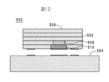
- FIG. 12 is a cross-sectional structure diagram of a wireless communication module 500 described in Patent Document 1.
- the wireless communication module 500 includes a multilayer substrate 502 and a main substrate 504.
- the multilayer substrate 502 is mounted on the main substrate 504.
- the multilayer substrate 502 includes a main body 506, a passive element 508, and a heat sink 510.
- the main body 506 is configured by laminating a plurality of dielectric layers in the vertical direction.
- the passive element 508 is accommodated in a space inside the main body 506.
- the heat sink 510 covers the passive element 508 from below so that the passive element 508 is not exposed to the outside.
- the heat sink 510 is joined to the external electrode of the main board 504 by solder. For this reason, the heat generated by the passive element 508 is transferred to the main substrate 504 through the heat sink 510.
- the wireless communication module 500 has a problem that the heat radiating plate 510 is easily detached from the main body 506.
- an object of the present invention is to provide a multilayer substrate and an electronic apparatus that can suppress the heat dissipation member from easily falling off from the base material.
- a multilayer substrate is a base material configured by stacking a plurality of insulator layers in a stacking direction, and has a mounting surface provided on one side of the stacking direction And an electronic component embedded in the base material, and the insulator layer between the surface of the electronic component on one side in the stacking direction and the mounting surface, and an external electrode of the electronic component Is a first heat dissipating member that is not electrically connected, and is made of a material having a second thermal conductivity higher than the first thermal conductivity of the material of the insulator layer.
- An electronic device is an electronic device including a mother substrate and a multilayer substrate mounted on the mother substrate, and the multilayer substrate includes a plurality of insulator layers stacked in a stacking direction.
- a substrate that is configured, the substrate having a mounting surface provided on one side in the stacking direction, an electronic component built in the substrate, and one of the electronic components in the stacking direction
- a first heat dissipating member that passes through the insulator layer between the side surface and the mounting surface and is not electrically connected to an external electrode of the electronic component,
- a first heat radiating member made of a material having a second thermal conductivity higher than the first thermal conductivity of the material, wherein the first heat radiating member is directly on the mother substrate.
- a fourth heat higher than the first thermal conductivity A first cross section that is connected to the mother substrate via a second bonding member made of a material having conductivity, and is orthogonal to the stacking direction in the first heat dissipation member; and the first A second cross section that is located on the other side in the stacking direction from the cross section and that is perpendicular to the stacking direction in the first heat radiating member, and when viewed from the stacking direction, There is a combination of the first cross section and the second cross section, the cross section of which protrudes from the first cross section.
- the present invention it is possible to prevent the heat dissipation member from easily falling off from the base material.
- FIG. 1 is a cross-sectional structure diagram of an electronic device 10 according to an embodiment of the present invention.
- FIG. 2A is a plan view of the heat dissipation member 50 from above.
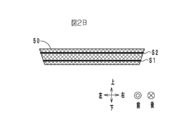
- 2B is a cross-sectional structure diagram in which the heat radiating member 50 of the electronic device 10 of FIG. 1 is extracted.
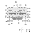
- FIG. 3 is a cross-sectional structure diagram of the electronic device 10 when it is manufactured.
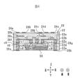
- FIG. 4 is a cross-sectional structure diagram of the electronic device 10 when it is manufactured.
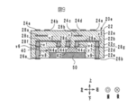
- FIG. 5 is a cross-sectional structure diagram of the electronic device 10 when it is manufactured.
- FIG. 6 is a cross-sectional structure diagram of an electronic apparatus 10a according to a first modification.
- FIG. 1 is a cross-sectional structure diagram of an electronic device 10 according to an embodiment of the present invention.
- FIG. 2A is a plan view of the heat dissipation member 50 from above.
- 2B is a cross-sectional structure diagram in which the heat radiating member
- FIG. 7A is a cross-sectional structure diagram of a multilayer substrate 20b according to a second modification.
- FIG. 7B is a cross-sectional structure diagram of a multilayer substrate 20c according to a third modification.
- FIG. 8 is a sectional structural view of a multilayer substrate 20d according to a fourth modification.
- FIG. 9 is a sectional structural view of a multilayer substrate 20e according to a fifth modification.
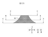
- FIG. 10A is a cross-sectional structure diagram orthogonal to the front-rear direction of the heat dissipation member 50 of the multilayer substrate 20f.
- FIG. 10B is a cross-sectional structure diagram orthogonal to the left-right direction of the heat dissipation member 50 of the multilayer substrate 20f.
- FIG. 10A is a cross-sectional structure diagram orthogonal to the front-rear direction of the heat dissipation member 50 of the multilayer substrate 20f.
- FIG. 10B is a cross-sectional structure
- FIG. 11A is a cross-sectional structure view taken along the line AA of the multilayer substrate 20f.
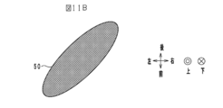
- FIG. 11B is a cross-sectional structure view taken along the line BB of the multilayer substrate 20f.
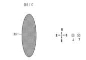
- FIG. 11C is a cross-sectional structure view taken along the line CC of the multilayer substrate 20f.
- FIG. 12 is an external perspective view of the wireless communication module 500 described in Patent Document 1.
- FIG. 1 is a cross-sectional structure diagram of an electronic device 10 according to an embodiment of the present invention.
- FIG. 2A is a plan view of the heat dissipation member 50 from above.
- 2B is a cross-sectional structure diagram in which the heat radiating member 50 of the electronic device 10 of FIG. 1 is extracted.
- the stacking direction of the multilayer substrate 20 is defined as the vertical direction.
- the left-right direction in FIG. 1 is defined as the left-right direction
- the direction perpendicular to the paper surface in FIG. 1 is defined as the front-rear direction.
- the up-down direction, the left-right direction, and the front-rear direction are orthogonal to each other.
- the electronic device 10 is, for example, a mobile phone, a personal computer, a game machine, a wearable terminal, or the like. In FIG. 1, only the modules provided in the electronic device 10 are illustrated, and the casing of the electronic device 10 and other configurations are omitted. As shown in FIG. 1, the electronic device 10 includes a multilayer substrate 20, chip components 60 and 70, and a mother substrate 100.
- the multilayer substrate 20 is a plate-like flexible substrate having a rectangular shape when viewed from above.
- the multilayer substrate 20 includes a base material 22, external electrodes 24a to 24e, 26a and 26b, wiring conductor layers 28a to 28g, via hole conductors v1 to v9, a semiconductor integrated circuit 40, and a heat dissipation member 50.
- the external electrodes are provided in addition to the external electrodes 24a to 24e, 26a, and 26b, but the external electrodes other than the external electrodes 24a to 24e, 26a, and 26b are omitted in FIG.
- wiring conductor layers are provided in addition to the wiring conductor layers 28a to 28g, but the wiring conductor layers other than the wiring conductor layers 28a to 28g are omitted in FIG.
- via hole conductors are provided in addition to the via hole conductors v1 to v9, but the via hole conductors other than the via hole conductors v1 to v9 are omitted in FIG.
- the base material 22 is a flexible plate-like member that forms a rectangle when viewed from above, as shown in FIG.
- the long side of the base material 22 extends in the left-right direction when viewed from above, and the short side of the base material 22 extends in the front-rear direction when viewed from above.
- the base material 22 is a laminate in which insulator sheets 22a to 22e (an example of a plurality of insulator layers) are laminated in this order from the upper side to the lower side.
- the base material 22 has two main surfaces.
- the main surface on the upper side (an example of the other side in the stacking direction) of the base material 22 is referred to as a front surface
- the main surface on the lower side of the base material 22 is referred to as a back surface.
- the back surface of the base material 22 is a mounting surface that faces the mother substrate 100 when the multilayer substrate 20 is mounted.
- the insulator sheets 22a to 22e are rectangular when viewed from above, and have the same shape as the base material 22.
- the insulator sheets 22a to 22e are insulator layers made of a material containing a flexible thermoplastic resin such as polyimide or liquid crystal polymer.
- a front surface the upper main surface of the insulator sheets 22a to 22e is referred to as a front surface
- the lower main surface of the insulator sheets 22a to 22e is referred to as a back surface.
- the external electrodes 24a to 24e are rectangular conductor layers and are provided on the surface of the insulator sheet 22a.
- the external electrodes 24a to 24e are arranged in a line in this order from the left side to the right side.
- External electrodes 26a and 26b are rectangular conductor layers, and are provided on the back surface (that is, the mounting surface) of the insulator sheet 22e.
- the external electrode 26 a is disposed near the left end of the base material 22, and the external electrode 26 b is disposed near the right end of the base material 22.
- the semiconductor integrated circuit 40 is a plate-shaped electronic component having a rectangular shape when viewed from above, and is built in the base material 22. More specifically, the semiconductor integrated circuit 40 includes a main body 42 and external electrodes 44a to 44c.
- the main body 42 has a rectangular plate shape when viewed from above.
- the upper main surface of the main body 42 is referred to as a front surface
- the lower surface of the main body 42 is referred to as a back surface.
- External electrodes 44 a to 44 c are rectangular conductor layers, and are provided on the surface of the main body 42.
- the external electrodes 44a to 44c are arranged in a line in this order from the left side to the right side.
- the semiconductor integrated circuit 40 is further provided with external electrodes (not shown) other than the external electrodes 44a to 44c. However, no external electrode is provided on the back surface of the main body 42.
- the insulator sheet 22d is provided with a rectangular hole penetrating in the vertical direction.
- the shape of the rectangular hole substantially matches the shape of the main body 42 when viewed from above. Further, the thickness in the vertical direction of the main body 42 is substantially the same as the thickness of the insulator sheet 22d. Therefore, the semiconductor integrated circuit 40 is accommodated in a hole provided in the insulator sheet 22d. Thereby, the semiconductor integrated circuit 40 is provided closer to the back surface than the front surface of the base material 22.
- the heat dissipation member 50 is a plate-like member having a rectangular shape when viewed from above.
- the upper main surface of the heat radiating member 50 is referred to as a front surface
- the lower surface of the heat radiating member 50 is referred to as a back surface.
- the solid line indicates the outer edge of the surface of the heat dissipation member 50
- the dotted line indicates the outer edge of the back surface of the heat dissipation member 50.
- the heat radiating member 50 has a quadrangular pyramid shape, and has a shape in which a cross section perpendicular to the vertical direction becomes smaller as it goes from the upper side to the lower side.
- a cross section S1 (an example of a first cross section) and a cross section S2 (a second cross section) are defined as follows.
- the cross section S1 is a cross section orthogonal to the vertical direction.
- the cross section S2 is a cross section that is located above the cross section S1 (an example of the other side in the stacking direction) and orthogonal to the vertical direction.
- the positions in the vertical direction of the cross sections S1 and S2 are arbitrary, and FIG. 2B shows an example thereof.
- the cross section S2 needs to be located above the cross section S1.
- the heat radiating member 50 there is a combination of cross sections S1 and S2 such that the cross section S2 protrudes from the cross section S1 when viewed from above.
- the combination of the cross sections S1 and S2 means that at least one combination of the cross sections S1 and S2 such that the cross section S2 protrudes from the cross section S1 exists, and the cross section S2 does not protrude from the cross section S1 This means that there may be a combination of such cross sections S1 and S2.
- the heat radiating member 50 has a square frustum shape, when viewed from above, the relationship in which the cross section S2 protrudes from the cross section S1 is established in all combinations with the cross sections S1 and S2. In other words, there is no combination of the cross sections S1 and S2 such that the cross section S2 does not protrude from the cross section S1. In addition, a relationship in which the area of the cross section S2 is larger than the area of the cross section S1 is established in all combinations of the cross sections S1 and S2. In other words, there is no combination of the cross sections S1 and S2 such that the area of the cross section S2 is equal to or smaller than the area of the cross section S1.
- the heat dissipation member 50 is a material having a thermal conductivity E2 (an example of the second thermal conductivity) higher than the thermal conductivity E1 (an example of the first thermal conductivity) of the material of the insulator sheets 22a to 22e. It is comprised by.
- the material of the heat dissipation member 50 is a metal plate made of a material such as copper.
- the heat radiating member 50 may be a plate made of a metal such as gold, aluminum, silver, or a carbon material.
- the heat radiating member 50 is not a combination of a conductor penetrating the insulator sheet 22e and a conductor layer or the like provided on the insulator sheet 22e, but a single member made of a single material. .
- the heat dissipation member 50 passes through the insulator sheet 22e between the back surface of the semiconductor integrated circuit 40 and the back surface of the base member 22, and is not electrically connected to the external electrodes 44a to 44c of the semiconductor integrated circuit 40. .
- the heat dissipation member 50 is provided on the insulator sheet 22e.
- the insulator sheet 22e is provided with a rectangular hole penetrating in the vertical direction. The shape of the rectangular hole provided in the insulator sheet 22e substantially matches the heat radiating member 50 when viewed from above. Further, the thickness of the heat dissipation member 50 in the vertical direction is substantially equal to the thickness of the insulator sheet 22e.
- the heat radiating member 50 is accommodated in the hole provided in the insulator sheet 22e. Thereby, the surface of the heat dissipation member 50 and the back surface of the semiconductor integrated circuit 40 are in direct contact.
- the rear surface of the semiconductor integrated circuit 40 and the front surface of the heat radiating member 50 are heat radiating grease or a conductor made of a material having a thermal conductivity E3 (an example of a third thermal conductivity) higher than the thermal conductivity E1. You may connect via paste etc. (an example of a 1st joining member).
- the heat radiating member 50 is maintained in a floating state.
- the floating state means a state where the conductor is not connected to a power supply potential or the like.
- the heat dissipating member 50 is not necessarily kept in a floating state, and may be connected to a ground potential, for example.
- the surface area of the heat dissipation member 50 is preferably 50% or more of the area of the back surface of the semiconductor integrated circuit 40 from the viewpoint of heat dissipation of the semiconductor integrated circuit 40.
- the heat radiating member 50 is relatively large, it is a concept that does not include a via-hole conductor or the like for connecting conductors between general layers.
- the wiring conductor layers 28 a to 28 g are linear conductor layers provided in the base material 22. More specifically, the wiring conductor layers 28a and 28b are provided on the surface of the insulator sheet 22b, and are arranged in this order from the left side to the right side.
- the wiring conductor layers 28c to 28e are provided on the surface of the insulator sheet 22c, and are arranged in this order from the left side to the right side.
- the wiring conductor layer 28c extends in the left-right direction. The right end of the wiring conductor layer 28c overlaps the external electrode 44a when viewed from above. The left end of the wiring conductor layer 28c overlaps the external electrode 26a when viewed from above.
- the wiring conductor layer 28d extends in the front-rear direction.
- the wiring conductor layer 28e extends in the left-right direction.
- the left end of the wiring conductor layer 28e overlaps the external electrode 44c when viewed from above.
- the right end of the wiring conductor layer 28e overlaps the external electrode 26b when viewed from above.
- the wiring conductor layer 28 f is provided on the surface of the insulator sheet 22 d and is disposed on the left side of the semiconductor integrated circuit 40.
- the wiring conductor layer 28f overlaps the left end of the wiring conductor layer 28c when viewed from above.
- the wiring conductor layer 28g is provided on the surface of the insulator sheet 22d and is disposed on the right side of the semiconductor integrated circuit 40.
- the wiring conductor layer 28g overlaps the right end of the wiring conductor layer 28e when viewed from above.
- the via-hole conductors v1 and v2 respectively penetrate the insulator sheet 22c in the vertical direction, and are arranged in this order from the left side to the right side.
- the via-hole conductors v1 and v2 have shapes that increase in thickness from the upper side to the lower side.
- the via-hole conductor v1 connects the left end of the wiring conductor layer 28c and the wiring conductor layer 28f.
- the via-hole conductor v2 connects the right end of the wiring conductor layer 28c and the external electrode 44a.
- the via-hole conductors v6 and v8 penetrate the insulator sheets 22d and 22e in the vertical direction, respectively, and are arranged on the left side of the semiconductor integrated circuit 40.
- the via-hole conductor v6 has a shape that increases in diameter from the upper side to the lower side.
- the via-hole conductor v8 has a shape that becomes thinner from the upper side to the lower side.
- the via-hole conductors v6 and v8 are connected to each other to form a series of via-hole conductors, and connect the wiring conductor layer 28f and the external electrode 26a.
- the via-hole conductors v1, v2, v6, v8 (an example of an interlayer connection conductor) and the wiring conductor layers 28c and 28f constitute a connection portion that connects the external electrode 44a and the external electrode 26a.
- the connection portion extends upward from the external electrode 44a, then extends toward the left side (an example of the orthogonal direction orthogonal to the stacking direction), and further extends downward. By doing so, it is connected to the external electrode 26a.
- the via-hole conductors v4 and v5 respectively penetrate the insulator sheet 22c in the vertical direction, and are arranged in this order from the left side to the right side.
- the via-hole conductors v4 and v5 have a shape that becomes thicker from the upper side to the lower side.
- the via-hole conductor v4 connects the left end of the wiring conductor layer 28e and the external electrode 44c.
- the via-hole conductor v5 connects the right end of the wiring conductor layer 28e and the wiring conductor layer 28g.
- the via-hole conductors v7 and v9 penetrate the insulator sheets 22d and 22e in the vertical direction, respectively, and are arranged on the right side of the semiconductor integrated circuit 40.
- the via-hole conductor v7 has a shape that increases in diameter from the upper side to the lower side.
- the via-hole conductor v9 has a shape that becomes thinner from the upper side to the lower side.
- the via-hole conductors v7 and v9 are connected to each other to form a series of via-hole conductors, and connect the wiring conductor layer 28g and the external electrode 26b.
- the via-hole conductors v4, v5, v7, v9 and the wiring conductor layers 28e, 28g constitute a connecting portion that connects the external electrode 44c and the external electrode 26b.
- the connection portion extends from the external electrode 44c toward the upper side, then extends toward the right side (an example of an orthogonal direction orthogonal to the stacking direction), and further extends toward the lower side. By doing so, it is connected to the external electrode 26b.
- the via-hole conductor v3 penetrates the insulating sheet 22c in the vertical direction and has a shape that becomes thicker from the upper side to the lower side.
- the via-hole conductor v3 connects the wiring conductor layer 28d and the external electrode 44b.
- the external electrode 44b is also connected to an external electrode (not shown) provided on the back surface of the substrate 22 via a via hole conductor v3 and a via hole conductor (not shown) and a wiring conductor layer.
- the material of the wiring conductor layers 28a to 28g and the external electrodes 24a to 24e, 26a, and 26b is, for example, copper. However, zinc plating is applied to the surfaces of the wiring conductor layers 28a to 28g and the external electrodes 24a to 24e, 26a, and 26b.
- the via-hole conductors v1 to v9 are obtained by solidifying a conductive paste mainly composed of a metal such as copper, tin, or silver.
- the chip components 60 and 70 are electronic components mounted on the surface of the multilayer substrate 20, and are, for example, capacitors and inductors. However, the chip components 60 and 70 may be semiconductor integrated circuits.
- the chip component 60 is mounted on the external electrodes 24a and 24b with solder.
- the chip component 70 is mounted on the external electrodes 24c to 24e by solder.
- the multilayer substrate 20 and the chip components 60 and 70 constitute a component mounting substrate. Note that the chip components 60 and 70 may not be arranged depending on the application. That is, you may comprise the multilayer substrate 20 which does not surface-mount components.
- the mother board 100 is a mother board such as a mobile phone, and is a large circuit board.
- the mother substrate 100 is basically a hard substrate that does not have flexibility, but may have flexibility.
- the mother substrate 100 includes a main body 102 and external electrodes 104a to 104c.
- the main body 102 is a plate-shaped multilayer substrate having a rectangular shape when viewed from above. An electric circuit is formed inside and on the surface of the main body 102.
- the upper main surface of the main body 102 is referred to as a front surface
- the lower main surface of the main body 102 is referred to as a back surface.
- External electrodes 104 a to 104 c are rectangular conductor layers and are provided on the surface of the main body 102.
- the external electrodes 104a to 104c are arranged in a line in this order from the left side to the right side.
- the external electrode 104b (an example of a third external electrode) is larger than the external electrodes 104a and 104c and has a shape that substantially matches the back surface of the heat dissipation member 50 when viewed from above.
- the mother substrate 100 is further provided with external electrodes (not shown) other than the external electrodes 104a to 104c.
- the multilayer board 20 is mounted on the mother board 100. More specifically, the external electrodes 26a and 26b are mounted on the external electrodes 104a and 104c by solders 110a and 110c, respectively.
- the heat dissipation member 50 is connected to the external electrode 104b via solder 110b (an example of a second bonding member).
- the material of the solder 110b has a thermal conductivity E4 (an example of a fourth thermal conductivity) that is higher than the thermal conductivity E1.
- E4 an example of a fourth thermal conductivity
- the heat of the heat radiating member 50 is transmitted to the external electrode 104b through the solder 110b.
- heat radiation grease or conductive paste may be used.
- the back surface of the heat dissipation member 50 and the external electrode 104b may be in direct contact with each other.
- FIG. 3 to 5 are cross-sectional structural views of the electronic device 10 when it is manufactured.
- a case where one multilayer substrate 20 is manufactured will be described as an example, but actually, a plurality of multilayer substrates 20 are manufactured simultaneously by laminating and cutting large-sized insulator sheets.
- insulator sheets 22a to 22e made of a liquid crystal polymer are prepared. Further, holes h1 and h2 penetrating vertically in the insulating sheets 22d and 22e are formed by punching, for example, with a punch or the like.
- a copper foil is formed on the entire main surface of one of the insulator sheets 22a to 22e. Specifically, copper foil is attached to the surfaces of the insulator sheets 22a to 22d. Copper foil is pasted on the back surface of the insulator sheet 22e. Further, the surface of the copper foil of the insulator sheets 22a to 22e is smoothed by applying, for example, zinc plating for rust prevention. In addition, metal foils other than copper foil may be used.
- the external electrodes 24a to 24e, the external electrodes (not shown) and the wiring conductor layer are formed on the surface of the insulator sheet 22a.
- a resist having the same shape as the external electrodes 24a to 24e shown in FIG. 3, the external electrodes not shown, and the wiring conductor layer is printed on the copper foil on the surface of the insulating sheet 22a.
- the copper foil of the part which is not covered with the resist is removed by performing an etching process with respect to copper foil. Thereafter, the resist is removed by spraying a cleaning liquid (resist removing liquid).
- a cleaning liquid resist removing liquid
- wiring conductor layers 28a to 28g are formed on the surfaces of the insulating sheets 22b to 22d, respectively. Further, as shown in FIG. 3, external electrodes 26a and 26b and an external electrode (not shown) are formed on the back surface of the insulator sheet 22e.
- the formation process of the wiring conductor layers 28a to 28g, the external electrodes 26a and 26b, and the external electrode (not shown) is the same as the formation process of the external electrodes 24a to 24e, the external electrode and the wiring conductor layer (not shown), and thus description thereof is omitted.
- a conductor layer such as a capacitor conductor layer (not shown) is present, the conductor layer is formed by the same formation process as that of the external electrodes 24a to 24e, the external electrode (not shown) and the wiring conductor layer.
- through holes are formed by irradiating laser beams to positions where the via hole conductors v1 to v9 and the via hole conductors (not shown) of the insulating sheets 22a to 22e are formed. Then, the through hole is filled with a conductive paste whose main component is a metal such as copper, tin or silver.
- the semiconductor integrated circuit 40 is disposed in the hole h1 of the insulator sheet 22d. Further, the heat dissipation member 50 is disposed in the hole h2 of the insulator sheet 22e. At this time, the heat radiating member 50 is inserted into the hole h2 from above.
- the multilayer substrate 20 is formed by thermocompression bonding. Specifically, as shown in FIG. 3, after the insulator sheets 22a to 22e are laminated, the insulator sheets 22a to 22e are subjected to pressure treatment and heat treatment (that is, thermocompression bonding). The pressurizing process is performed by sandwiching the insulator sheets 22a to 22e from above and below. By applying pressure treatment and heat treatment to the insulator sheets 22a to 22e, the insulator sheets 22a to 22e are softened and the conductive paste in the through holes is solidified. Thereby, the insulator sheets 22a to 22e are joined, and the via-hole conductors v1 to v9 are formed.
- pressure treatment and heat treatment that is, thermocompression bonding
- thermoplastic resin of the insulator sheets 22a to 22e flows by the pressurizing process and the heat process, so that the inner peripheral surfaces of the holes h1 and h2 are in close contact with the shapes of the semiconductor integrated circuit 40 and the heat dissipation member 50.
- the multilayer substrate 20 is completed as shown in FIG.
- the chip parts 60 and 70 are mounted on the multilayer substrate 20 by soldering. Thereby, a component mounting board is completed.
- the multilayer substrate 20 is mounted on the mother substrate 100 by soldering.
- the electronic device 10 is completed by mounting the mother substrate 100 on the housing.
- the heat radiating member 50 passes through the insulator sheet 22 e between the back surface of the semiconductor integrated circuit 40 and the back surface of the base material 22.
- the thermal conductivity E1 the thermal conductivity of the heat radiating member 50 and the mother substrate 100.
- it can be connected via a heat dissipating grease made of a material having a high thermal conductivity.
- the semiconductor integrated circuit 40 is provided closer to the back surface than the front surface of the base material 22. Therefore, heat generated in the semiconductor integrated circuit 40 is transmitted to the mother substrate 100 through a shorter path. Therefore, according to the multilayer substrate 20 and the electronic device 10, higher heat dissipation can be obtained.
- the multilayer substrate 20 and the electronic device 10 it is possible to suppress the heat radiating member 50 from easily falling off from the base material 22.
- a multilayer substrate according to a comparative example of the multilayer substrate 20 a multilayer substrate including a heat radiation member having a rectangular parallelepiped shape instead of a square frustum shape will be described as an example.
- Other configurations of the multilayer substrate according to the comparative example are the same as those of the multilayer substrate 20. Therefore, the reference numerals of the multilayer board 20 are used as the reference numerals of the multilayer board according to the comparative example.
- the heat radiating member 50 penetrates the insulator sheet 22e from the back surface of the semiconductor integrated circuit 40 to the back surface of the base member 22. Furthermore, the cross-sectional shape of the heat dissipation member 50 is a rectangular shape. Therefore, the heat radiating member 50 is held by the base material 22 when the side surface of the heat radiating member 50 is in close contact with the inner peripheral surface of the hole of the insulator sheet 22e. Therefore, when a strong impact is applied to the multilayer substrate according to the comparative example, the heat dissipation member 50 may fall off the base material 22.
- the multilayer substrate 20 and the electronic device 10 there is a combination of the cross sections S1 and S2 such that the cross section S2 protrudes from the cross section S1 when viewed from above.
- the cross section S2 is caught on the inner peripheral surface of the hole of the insulator sheet 22e.
- the heat radiating member 50 is prevented from falling off the base material 22.
- the multilayer substrate 20 and the electronic device 10 it can suppress more effectively that the thermal radiation member 50 falls from the base material 22 easily. Since the heat radiating member 50 has a square frustum shape, when viewed from above, the relationship in which the cross section S2 protrudes from the cross section S1 is established in all combinations with the cross sections S1 and S2. As a result, the heat radiating member 50 cannot move downward even slightly. As a result, according to the multilayer substrate 20 and the electronic device 10, it is possible to more effectively suppress the heat dissipation member 50 from easily falling off from the base material 22.
- the multilayer substrate 20 and the electronic device 10 it can suppress more effectively that the thermal radiation member 50 falls from the base material 22 easily. Since the heat radiating member 50 has a square frustum shape, the relationship in which the area of the cross section S2 is larger than the area of the cross section S1 is established in all combinations of the cross sections S1 and S2. Thereby, the amount that the cross section S2 protrudes from the cross section S1 increases. As a result, according to the multilayer substrate 20 and the electronic device 10, it is possible to more effectively suppress the heat dissipation member 50 from easily falling off from the base material 22.
- the heat dissipation member 50 is connected to the external electrode 104b via the solder 110b. Thereby, it is suppressed that a gap is formed between the heat dissipation member 50 and the external electrode 104b. As a result, heat is efficiently transferred from the heat dissipation member 50 to the external electrode 104b.
- the multilayer substrate 20 and the electronic device 10 higher heat dissipation can be obtained for the following reason. More specifically, when the heat radiating member 50 is connected to the semiconductor integrated circuit 40 through heat radiating grease or the like, the formation of a gap between the heat radiating member 50 and the semiconductor integrated circuit 40 is suppressed. As a result, heat is efficiently transferred from the semiconductor integrated circuit 40 to the heat dissipation member 50.
- the multilayer substrate 20 and the electronic device 10 it is possible to reduce the influence of heat on the signals, power supply currents, and the like that flow between the external electrodes 44a and 44c and the external electrodes 26a and 26b.
- the connection from the external electrode 44a to the external electrode 26a will be described below as an example.
- the via-hole conductors v1, v2, v6, v8 and the wiring conductor layers 28c, 28f form a connection portion that connects the external electrode 44a and the external electrode 26a.
- the connection portion extends upward from the external electrode 44a, then extends toward the left side, and further extends downward to be connected to the external electrode 26a. Thereby, a connection part comes to avoid the heat radiating member 50.
- FIG. As a result, it is possible to reduce the influence of heat on the signal, power supply current, etc. flowing between the external electrode 44a and the external electrode 26a.
- the side surface of the heat radiating member 50 is a smooth inclined surface. Therefore, the insulator sheet 22e is easily adhered to the side surface of the heat dissipation member 50. As a result, the heat dissipation member 50 is more effectively suppressed from falling off the base material 22.
- FIG. 6 is a cross-sectional structure diagram of an electronic apparatus 10a according to a first modification.
- the multilayer substrate 20a is different from the multilayer substrate 20 in that it further includes heat dissipation members 50a and 50b, wiring conductor layers 28h to 28j, via-hole conductors v10 and v11, and an insulator sheet 22f.
- the multilayer substrate 20a will be described focusing on the difference.
- the base material 22 is configured by laminating insulator sheets 22a to 22f in this order from the upper side to the lower side.
- the wiring conductor layer 28h is provided on the surface of the insulator sheet 22f.
- the wiring conductor layer 28h overlaps the left end of the wiring conductor layer 28a when viewed from above, and is connected to the lower end of the via-hole conductor v8.
- the via-hole conductor v10 penetrates the insulator sheet 22f in the vertical direction, and connects the wiring conductor layer 28h and the external electrode 26a.
- the wiring conductor layer 28i is provided on the surface of the insulator sheet 22f.
- the wiring conductor layer 28j overlaps with the right end of the wiring conductor layer 28e when viewed from above, and is connected to the lower end of the via-hole conductor v9.
- the via-hole conductor v11 penetrates the insulator sheet 22f in the vertical direction, and connects the wiring conductor layer 28j and the external electrode 26b.
- the heat radiating members 50a and 50b penetrate through the insulator sheets 22e and 22f between the back surface of the semiconductor integrated circuit 40 and the back surface of the base member 22, and are electrically connected to the external electrodes 44a to 44c of the semiconductor integrated circuit 40. Not connected.
- the heat radiating members 50a and 50b are arranged at intervals in this order from the left side to the right side.
- the wiring conductor layer 28i is provided between the heat dissipation member 50a (an example of the first heat dissipation member) and the heat dissipation member 50b (an example of the second heat dissipation member) in the left-right direction (an example of the orthogonal direction).
- the shape of the heat radiating members 50 a and 50 b is a quadrangular pyramid like the heat radiating member 50. However, the heat dissipation members 50 a and 50 b are thinner than the heat dissipation member 50.
- the heat radiating members 50a and 50b are constituted by plate-like members or block-like members made of, for example, copper.
- description is abbreviate
- the same operational effects as the multilayer substrate 20 and the electronic device 10 can be obtained.
- the degree of freedom in designing the multilayer substrate 20a is increased. More specifically, the density of the wiring conductor layer increases near the back surface of the multilayer substrate 20a. Therefore, in the multilayer substrate 20a, the heat dissipation member 50 is separated into two heat dissipation members 50a and 50b. As a result, the space in which the wiring conductor layer can be provided is widened, so that the degree of freedom in designing the multilayer substrate 20a is increased.
- FIG. 7A is a cross-sectional structure diagram of a multilayer substrate 20b according to a second modification.
- the multilayer substrate 20 b is different from the multilayer substrate 20 in the shape of the heat dissipation member 50.
- the multilayer substrate 20b will be described focusing on the difference.
- the side surface of the heat dissipation member 50 has a step. More specifically, when viewed from above, the upper half of the heat radiating member 50 is slightly larger than the lower half of the heat radiating member 50 and protrudes in the front-rear direction and the left-right direction from the lower half of the heat radiating member 50. .
- the heat radiation member 50 has a step on the side surface. Therefore, when the heat radiating member 50 is produced with the metal plate or the metal block, the heat radiating member 50 can be processed easily.
- FIG. 7B is a cross-sectional structure diagram of a multilayer substrate 20c according to a third modification.
- the heat radiating member 50 is provided across the insulator sheets 22e and 22f. More specifically, the heat radiating member 50 of the multilayer substrate 20c has a step on the side surface in the same manner as the heat radiating member 50 of the multilayer substrate 20b. However, in the multilayer substrate 20c, the upper half of the heat dissipation member 50 is accommodated in a hole provided in the insulator sheet 22e, and the lower half of the heat dissipation member 50 is accommodated in a hole provided in the insulator sheet 22f.
- the same effects as the multilayer substrate 20 can be achieved.
- the multilayer substrate 20c unlike the multilayer substrate 20b, it is not necessary to provide a level
- FIG. 8 is a sectional structural view of a multilayer substrate 20d according to a fourth modification.
- the multilayer substrate 20 d is different from the multilayer substrate 20 in the shape of the heat dissipation member 50.
- the multilayer substrate 20d will be described focusing on the difference.
- the cross section perpendicular to the vertical direction of the heat dissipation member 50 is large at the center of the heat dissipation member 50 in the vertical direction. And the cross section becomes small as it approaches the front surface and the back surface of the heat radiating member 50. Even in the heat radiating member 50 having such a shape, there is a combination of cross sections S1 and S2 such that the cross section S2 protrudes from the cross section S1 when viewed from above. Therefore, the multilayer substrate 20 d can also exhibit the same operational effects as the multilayer substrate 20.
- FIG. 9 is a sectional structural view of a multilayer substrate 20e according to a fifth modification.
- the multilayer substrate 20 e is different from the multilayer substrate 20 in the shape of the heat dissipation member 50.
- the multilayer substrate 20e will be described focusing on the difference.
- the cross section perpendicular to the vertical direction of the heat dissipation member 50 is the smallest at the center of the heat dissipation member 50 in the vertical direction. And the cross section becomes large as it approaches the surface and the back surface of the heat radiating member 50. Even in the heat radiating member 50 having such a shape, there is a combination of cross sections S1 and S2 such that the cross section S2 protrudes from the cross section S1 when viewed from above. Therefore, the multilayer substrate 20 e can also exhibit the same operational effects as the multilayer substrate 20.
- FIG. 10A is a cross-sectional structure diagram orthogonal to the front-rear direction of the heat dissipation member 50 of the multilayer substrate 20f.
- FIG. 10B is a cross-sectional structure diagram orthogonal to the left-right direction of the heat dissipation member 50 of the multilayer substrate 20f.
- FIG. 11A is a cross-sectional structure view taken along the line AA of the multilayer substrate 20f.
- FIG. 11B is a cross-sectional structure view taken along the line BB of the multilayer substrate 20f.
- FIG. 11C is a cross-sectional structure view taken along the line CC of the multilayer substrate 20f.
- the size and shape of a cross section orthogonal to the vertical direction are constant regardless of the vertical position of the heat radiating member 50. More specifically, the heat radiating member 50 has an elliptical cross section, as shown in FIGS. 11A to 11C. However, on the back surface of the heat radiating member 50, as shown in FIG. 11A, the cross section of the heat radiating member 50 forms an ellipse having a long axis parallel to the left-right direction. And the elliptical cross section of the heat radiating member 50 rotates counterclockwise as it goes from the lower side to the upper side. And as shown to FIG.
- the surface of the thermal radiation member 50 has comprised the ellipse which has a long axis parallel to the front-back direction.
- the cross sections S1 and S2 may be equal, or although not shown, the cross section S1 may be larger than the cross section S2 in all combinations of the cross sections S1 and S2.
- the multilayer substrate and the electronic device according to the present invention are not limited to the multilayer substrates 20, 20a to 20f and the electronic devices 10 and 10a, and can be changed within the scope of the gist thereof.
- the configurations of the multilayer substrates 20, 20a to 20f and the electronic devices 10, 10a may be arbitrarily combined.
- the back surface of the heat radiating member 50, 50a, 50b may be plated.
- the back surface of the thermal radiation member 50, 50a, 50b may be covered by providing an external electrode in the back surface of the base material 22.
- FIG. When the back surfaces of the heat radiating members 50, 50 a, 50 b are covered with the external electrodes, the heat radiating members 50, 50 a, 50 b are more effectively suppressed from falling off the base material 22.
- the plating film and the external electrode as described above function as a joining member that mediates the connection between the heat radiation members 50, 50a, and 50b and the external electrode 104b.
- the present invention is useful for a multilayer substrate and an electronic device, and more specifically, is excellent in that the heat dissipation member can be prevented from easily falling off from the base material.
Landscapes
- Engineering & Computer Science (AREA)
- Microelectronics & Electronic Packaging (AREA)
- Manufacturing & Machinery (AREA)
- Cooling Or The Like Of Semiconductors Or Solid State Devices (AREA)
- Production Of Multi-Layered Print Wiring Board (AREA)
- Structure Of Printed Boards (AREA)
- Chemical & Material Sciences (AREA)
- Materials Engineering (AREA)
Abstract
基材から放熱部材が容易に脱落することを抑制できる多層基板及び電子機器を提供することである。 本発明に係る多層基板は、積層方向の一方側に設けられている実装面を有する基材と、基材に内蔵されている電子部品と、電子部品の積層方向の一方側の面から実装面までの間の絶縁体層を貫通し、かつ、電子部品の外部電極には電気的に接続されていない放熱部材であって、絶縁体層の材料の第1の熱伝導率よりも高い第2の熱伝導率を有する材料により構成されている放熱部材と、を備えており、放熱部材において積層方向に直交する第1の断面、及び、第1の断面よりも積層方向の他方側に位置し、かつ、放熱部材において積層方向に直交する第2の断面を定義し、積層方向から見たときに、第2の断面が第1の断面からはみ出すような第1の断面と第2の断面との組み合わせが存在していること、を特徴とする。
Description
本発明は、電子部品を内蔵している多層基板及び電子機器に関する。
従来の多層基板に関する発明としては、例えば、特許文献1に記載の無線通信モジュールが知られている。図12は、特許文献1に記載の無線通信モジュール500の断面構造図である。
無線通信モジュール500は、多層基板502及び主基板504を備えている。多層基板502は、主基板504上に実装されている。多層基板502は、本体506、受動素子508及び放熱板510を含んでいる。本体506は、複数の誘電体層が上下方向に積層されて構成されている。受動素子508は、本体506内の空間に収容されている。放熱板510は、受動素子508が外部に露出しないように、受動素子508を下側から覆っている。
以上のような無線通信モジュール500では、放熱板510は、主基板504の外部電極に対してはんだにより接合されている。このため、受動素子508が発生した熱は、放熱板510を介して主基板504へと伝達される。
ところで、無線通信モジュール500は、放熱板510が本体506から脱落しやすいという問題を有する。
そこで、本発明の目的は、基材から放熱部材が容易に脱落することを抑制できる多層基板及び電子機器を提供することである。
本発明の一形態に係る多層基板は、複数の絶縁体層が積層方向に積層されて構成されている基材であって、該積層方向の一方側に設けられている実装面を有する基材と、前記基材に内蔵されている電子部品と、前記電子部品の前記積層方向の一方側の面から前記実装面までの間の前記絶縁体層を貫通し、かつ、該電子部品の外部電極には電気的に接続されていない第1の放熱部材であって、前記絶縁体層の材料の第1の熱伝導率よりも高い第2の熱伝導率を有する材料により構成されている第1の放熱部材と、を備えており、前記第1の放熱部材において前記積層方向に直交する第1の断面、及び、該第1の断面よりも該積層方向の他方側に位置し、かつ、該第1の放熱部材において該積層方向に直交する第2の断面を定義し、前記積層方向から見たときに、前記第2の断面が前記第1の断面からはみ出すような該第1の断面と該第2の断面との組み合わせが存在していること、を特徴とする。
本発明の一形態に係る電子機器は、マザー基板及び該マザー基板に実装されている多層基板を備えた電子機器であって、前記多層基板は、複数の絶縁体層が積層方向に積層されて構成されている基材であって、該積層方向の一方側に設けられている実装面を有する基材と、前記基材に内蔵されている電子部品と、前記電子部品の前記積層方向の一方側の面から前記実装面までの間の前記絶縁体層を貫通し、かつ、該電子部品の外部電極には電気的に接続されていない第1の放熱部材であって、前記絶縁体層の材料の第1の熱伝導率よりも高い第2の熱伝導率を有する材料により構成されている第1の放熱部材と、を備えており、前記第1の放熱部材は、前記マザー基板に直接に接しているか、又は、前記第1の熱伝導率よりも高い第4の熱伝導率を有する材料により構成されている第2の接合部材を介して該マザー基板に接続されており、前記第1の放熱部材において前記積層方向に直交する第1の断面、及び、該第1の断面よりも該積層方向の他方側に位置し、かつ、該第1の放熱部材において該積層方向に直交する第2の断面を定義し、前記積層方向から見たときに、前記第2の断面が前記第1の断面からはみ出すような該第1の断面と該第2の断面との組み合わせが存在していること、を特徴とする。
本発明によれば、基材から放熱部材が容易に脱落することを抑制できる。
(実施形態)
<多層基板及び電子機器の構成>
以下に、本発明の一実施形態に係る多層基板及び電子機器の構成について図面を参照しながら説明する。図1は、本発明の一実施形態に係る電子機器10の断面構造図である。図2Aは、放熱部材50を上側から平面視した図である。図2Bは、図1の電子機器10の放熱部材50を抽出した断面構造図である。以下では、多層基板20の積層方向を上下方向と定義する。図1の左右方向を左右方向と定義し、図1の紙面の垂直方向を前後方向と定義する。上下方向、左右方向及び前後方向は互いに直交している。
<多層基板及び電子機器の構成>
以下に、本発明の一実施形態に係る多層基板及び電子機器の構成について図面を参照しながら説明する。図1は、本発明の一実施形態に係る電子機器10の断面構造図である。図2Aは、放熱部材50を上側から平面視した図である。図2Bは、図1の電子機器10の放熱部材50を抽出した断面構造図である。以下では、多層基板20の積層方向を上下方向と定義する。図1の左右方向を左右方向と定義し、図1の紙面の垂直方向を前後方向と定義する。上下方向、左右方向及び前後方向は互いに直交している。
電子機器10は、例えば、携帯電話やパーソナルコンピュータ、ゲーム機、ウェラブル端末等である。図1では、電子機器10内に設けられているモジュールのみを図示し、電子機器10の筐体やその他の構成については省略した。電子機器10は、図1に示すように、多層基板20、チップ部品60,70及びマザー基板100を備えている。
まず、多層基板20について説明する。多層基板20は、上側から見たときに長方形状をなす板状のフレキシブル基板である。多層基板20は、図1に示すように、基材22、外部電極24a~24e,26a,26b、配線導体層28a~28g、ビアホール導体v1~v9、半導体集積回路40及び放熱部材50を備えている。なお、外部電極は、外部電極24a~24e,26a,26b以外にも設けられているが、外部電極24a~24e,26a,26b以外の外部電極については図1では省略した。同様に、配線導体層は、配線導体層28a~28g以外にも設けられているが、配線導体層28a~28g以外の配線導体層については図1では省略した。同様に、ビアホール導体は、ビアホール導体v1~v9以外にも設けられているが、ビアホール導体v1~v9以外のビアホール導体については図1では省略した。
基材22は、図1に示すように、上側から見たときに、長方形をなす可撓性の板状部材である。基材22の長辺は、上側から見たときに、左右方向に延在しており、基材22の短辺は、上側から見たときに、前後方向に延在している。基材22は、絶縁体シート22a~22e(複数の絶縁体層の一例)が上側から下側へとこの順に積層されて構成されている積層体である。基材22は、2つの主面を有している。以下では、基材22の上側(積層方向の他方側の一例)の主面を表面と称し、基材22の下側(積層方向の一方側の一例)の主面を裏面と称す。基材22の裏面は、多層基板20の実装時にマザー基板100に対向する実装面である。
絶縁体シート22a~22eは、上側から見たときに、長方形状をなしており、基材22と同じ形状をなしている。絶縁体シート22a~22eは、ポリイミドや液晶ポリマ等の可撓性を有する熱可塑性樹脂を含む材料により作製されている絶縁体層である。以下では、絶縁体シート22a~22eの上側の主面を表面と称し、絶縁体シート22a~22eの下側の主面を裏面と称す。
外部電極24a~24eは、長方形状の導体層であり、絶縁体シート22aの表面に設けられている。外部電極24a~24eは、左側から右側へとこの順に一列に並ぶように配置されている。
外部電極26a,26b(第2の外部電極の一例)は、長方形状の導体層であり、絶縁体シート22eの裏面(すなわち、実装面)に設けられている。外部電極26aは、基材22の左端近傍に配置され、外部電極26bは、基材22の右端近傍に配置されている。
半導体集積回路40は、上側から見たときに、長方形状をなす板状の電子部品であり、基材22に内蔵されている。より詳細には、半導体集積回路40は、本体42及び外部電極44a~44cを含んでいる。本体42は、上側から見たときに、長方形状をなす板状をなしている。以下では、本体42の上側の主面を表面と称し、本体42の下側の面を裏面と称す。
外部電極44a~44c(第1の外部電極の一例)は、長方形状の導体層であり、本体42の表面に設けられている。外部電極44a~44cは、左側から右側へとこの順に一列に並ぶように配置されている。なお、半導体集積回路40には、外部電極44a~44c以外の図示しない外部電極が更に設けられている。ただし、本体42の裏面には外部電極が設けられていない。
絶縁体シート22dには、上下方向に貫通する長方形状の孔が設けられている。長方形状の孔の形状は、上側から見たときに、本体42の形状と略一致している。また、本体42の上下方向の厚みは、絶縁体シート22dの厚みと略一致している。よって、半導体集積回路40は、絶縁体シート22dに設けられた孔に収容されている。これにより、半導体集積回路40は、基材22の表面よりも裏面の近くに設けられている。
放熱部材50は、図2Aに示すように、上側から見たときに、長方形状をなす板状の部材である。以下では、放熱部材50の上側の主面を表面と称し、放熱部材50の下側の面を裏面と称す。図2Aにおいて、実線は放熱部材50の表面の外縁を示し、点線は放熱部材50の裏面の外縁を示している。放熱部材50は、四角錐台形状をなしており、上側から下側へと行くにしたがって、上下方向に直交する断面が小さくなる形状を有している。
以下に、放熱部材50の形状についてより詳細に説明する。図2Bに示すように、放熱部材50において断面S1(第1の断面の一例)及び断面S2(第2の断面)を以下のように定義する。断面S1は、上下方向に直交する断面である。断面S2は、断面S1よりも上側(積層方向の他方側の一例)に位置し、かつ、上下方向に直交する断面である。断面S1,S2の上下方向における位置は任意であり、図2Bではその一例を示した。ただし、断面S2が断面S1よりも上側に位置している必要がある。
放熱部材50では、上側から見たときに、断面S2が断面S1からはみ出すような断面S1,S2の組み合わせが存在している。断面S1,S2の組み合わせが存在しているとは、断面S2が断面S1からはみ出すような断面S1,S2の組み合わせが少なくとも1組だけ存在していればよく、断面S2が断面S1からはみ出さないような断面S1,S2の組み合わせが存在してもよいという意味である。
ただし、放熱部材50が四角錘台形状をなしているので、上側から見たときに、断面S2が断面S1からはみ出す関係が、全ての断面S1,S2との組み合わせにおいて成立している。換言すれば、断面S2が断面S1からはみ出さないような断面S1,S2の組み合わせが存在していない。加えて、断面S2の面積が断面S1の面積よりも大きい関係が、全ての断面S1,S2の組み合わせにおいて成立している。換言すれば、断面S2の面積が断面S1の面積以下となるような断面S1,S2の組み合わせが存在していない。
また、放熱部材50は、絶縁体シート22a~22eの材料の熱伝導率E1(第1の熱伝導率の一例)よりも高い熱伝導率E2(第2の熱伝導率の一例)を有する材料により構成されている。本実施形態では、放熱部材50の材料は、銅等の材料からなる金属板である。ただし、放熱部材50は、金、アルミニウム、銀等の金属や、炭素材料等の材料からなる板であってもよい。なお、放熱部材50は、絶縁体シート22eを貫通する導体と絶縁体シート22eに設けられている導体層等の組み合わせではなく、単一の材料から構成される単一の部材であることが好ましい。
放熱部材50は、半導体集積回路40の裏面から基材22の裏面までの間の絶縁体シート22eを貫通し、かつ、半導体集積回路40の外部電極44a~44cには電気的に接続されていない。本実施形態では、放熱部材50は、絶縁体シート22eに設けられている。また、絶縁体シート22eには、上下方向に貫通する長方形状の孔が設けられている。絶縁体シート22eに設けられている長方形状の孔の形状は、上側から見たときに、放熱部材50とほぼ一致している。また、放熱部材50の上下方向の厚みは、絶縁体シート22eの厚みと略一致している。よって、放熱部材50は、絶縁体シート22eに設けられた孔に収容されている。これにより、放熱部材50の表面と半導体集積回路40の裏面とは直接に接している。ただし、半導体集積回路40の裏面と放熱部材50の表面とは、熱伝導率E1よりも高い熱伝導率E3(第3の熱伝導率の一例)を有する材料により構成されている放熱グリスや導体ペースト等(第1の接合部材の一例)を介して接続されてもよい。
また、本体42の裏面には外部電極が設けられていないので、放熱部材50の表面は本体42の外部電極とは接触していない。これにより、放熱部材50は、フローティング状態に保たれる。フローティング状態とは、導体が電源電位等に接続されていない状態を意味する。ただし、放熱部材50は、必ずしもフローティング状態に保たれる必要はなく、例えば、グランド電位に接続されていてもよい。また、放熱部材50の表面の面積は、半導体集積回路40の放熱性の観点から、半導体集積回路40の裏面の面積の50%以上であることが好ましい。このように、放熱部材50は、比較的に大きいので、一般的な層間の導体同士を接続するためのビアホール導体等を含まない概念である。
配線導体層28a~28g(配線導体層の一例)は、基材22内に設けられている線状の導体層である。より詳細には、配線導体層28a,28bは、絶縁体シート22bの表面に設けられており、左側から右側へとこの順に並んでいる。配線導体層28c~28eは、絶縁体シート22cの表面に設けられており、左側から右側へとこの順に並んでいる。配線導体層28cは、左右方向に延在している。配線導体層28cの右端は、上側から見たときに、外部電極44aと重なっている。配線導体層28cの左端は、上側から見たときに、外部電極26aと重なっている。配線導体層28dは、前後方向に延在している。配線導体層28eは、左右方向に延在している。配線導体層28eの左端は、上側から見たときに、外部電極44cと重なっている。配線導体層28eの右端は、上側から見たときに、外部電極26bと重なっている。配線導体層28fは、絶縁体シート22dの表面に設けられており、半導体集積回路40よりも左側に配置されている。配線導体層28fは、上側から見たときに、配線導体層28cの左端と重なっている。配線導体層28gは、絶縁体シート22dの表面に設けられており、半導体集積回路40よりも右側に配置されている。配線導体層28gは、上側から見たときに、配線導体層28eの右端と重なっている。
ビアホール導体v1,v2はそれぞれ、絶縁体シート22cを上下方向に貫通しており、左側から右側へとこの順に並んでいる。ビアホール導体v1,v2は、上側から下側に行くにしたがって太くなる形状をなしている。ビアホール導体v1は、配線導体層28cの左端と配線導体層28fとを接続している。ビアホール導体v2は、配線導体層28cの右端と外部電極44aとを接続している。
ビアホール導体v6,v8はそれぞれ、絶縁体シート22d,22eを上下方向に貫通しており、半導体集積回路40よりも左側に配置されている。ビアホール導体v6は、上側から下側に行くにしたがって直径が太くなる形状をなしている。ビアホール導体v8は、上側から下側に行くにしたがって細くなる形状をなしている。ビアホール導体v6,v8は、互いに接続されることにより1連のビアホール導体を構成しており、配線導体層28fと外部電極26aとを接続している。これにより、ビアホール導体v1,v2,v6,v8(層間接続導体の一例)及び配線導体層28c,28fは、外部電極44aと外部電極26aとを接続する接続部を構成している。本実施形態では、接続部は、外部電極44aから上側に向かって延在した後、左側(積層方向に直交する直交方向の一例)に向かって延在し、更に、下側に向かって延在することにより、外部電極26aに接続されている。
ビアホール導体v4,v5はそれぞれ、絶縁体シート22cを上下方向に貫通しており、左側から右側へとこの順に並んでいる。ビアホール導体v4,v5は、上側から下側に行くにしたがって太くなる形状をなしている。ビアホール導体v4は、配線導体層28eの左端と外部電極44cとを接続している。ビアホール導体v5は、配線導体層28eの右端と配線導体層28gとを接続している。
ビアホール導体v7,v9はそれぞれ、絶縁体シート22d,22eを上下方向に貫通しており、半導体集積回路40よりも右側に配置されている。ビアホール導体v7は、上側から下側に行くにしたがって直径が太くなる形状をなしている。ビアホール導体v9は、上側から下側に行くにしたがって細くなる形状をなしている。ビアホール導体v7,v9は、互いに接続されることにより1連のビアホール導体を構成しており、配線導体層28gと外部電極26bとを接続している。これにより、ビアホール導体v4,v5,v7,v9及び配線導体層28e,28gは、外部電極44cと外部電極26bとを接続する接続部を構成している。本実施形態では、接続部は、外部電極44cから上側に向かって延在した後、右側(積層方向に直交する直交方向の一例)に向かって延在し、更に、下側に向かって延在することにより、外部電極26bに接続されている。
ビアホール導体v3は、絶縁体シート22cを上下方向に貫通しており、上側から下側に行くにしたがって太くなる形状をなしている。ビアホール導体v3は、配線導体層28dと外部電極44bとを接続している。なお、外部電極44bも、ビアホール導体v3及び図示しないビアホール導体及び配線導体層を介して、基材22の裏面に設けられている図示しない外部電極に接続されている。
配線導体層28a~28g及び外部電極24a~24e,26a,26bの材料は、例えば、銅である。ただし、配線導体層28a~28g及び外部電極24a~24e,26a,26bの表面には亜鉛鍍金が施されている。また、ビアホール導体v1~v9は、銅、錫や銀等の金属を主成分とする導電性ペーストが固化したものである。
次に、チップ部品60,70について説明する。チップ部品60,70は、多層基板20の表面上に実装される電子部品であり、例えば、コンデンサやインダクタ等である。ただし、チップ部品60,70は、半導体集積回路であってもよい。チップ部品60は、外部電極24a,24bにはんだにより実装される。チップ部品70は、外部電極24c~24eにはんだにより実装される。多層基板20及びチップ部品60,70は、部品実装基板を構成している。なお、用途によってはチップ部品60,70は配置されていなくてもよい。すなわち、部品を表面実装しない多層基板20を構成していてもよい。
次に、マザー基板100について説明する。マザー基板100は、携帯電話等のマザーボードであり、大判の回路基板である。マザー基板100は、基本的には、可撓性を有さない硬質な基板であるが、可撓性を有していてもよい。マザー基板100は、本体102及び外部電極104a~104cを含んでいる。本体102は、上側から見たときに、長方形状をなす板状の多層基板である。本体102の内部及び表面には電気回路が形成されている。以下では、本体102の上側の主面を表面と称し、本体102の下側の主面を裏面と称す。
外部電極104a~104cは、長方形状の導体層であり、本体102の表面に設けられている。外部電極104a~104cは、左側から右側へとこの順に一列に並ぶように配置されている。外部電極104b(第3の外部電極の一例)は、外部電極104a,104cよりも大きく、上側から見たときに、放熱部材50の裏面と略一致する形状を有している。なお、マザー基板100には、外部電極104a~104c以外の図示しない外部電極が更に設けられている。
多層基板20は、マザー基板100に実装されている。より詳細には、外部電極26a,26bはそれぞれ、外部電極104a,104cに対してはんだ110a,110cにより実装されている。また、放熱部材50は、はんだ110b(第2の接合部材の一例)を介して外部電極104bに接続されている。はんだ110bの材料は、熱伝導率E1よりも高い熱伝導率E4(第4の熱伝導率の一例)を有する。これにより、放熱部材50の熱は、はんだ110bを介して外部電極104bへと伝達される。はんだ110bの代わりに放熱グリスや導体ペーストが用いられてもよい。また、放熱部材50の裏面と外部電極104bとは直接に接していてもよい。
<電子機器の製造方法>
以下に、電子機器10の製造方法について図面を参照しながら説明する。図3ないし図5は、電子機器10の製造時の断面構造図である。以下では、一つの多層基板20が作製される場合を例にとって説明するが、実際には、大判の絶縁体シートが積層及びカットされることにより、同時に複数の多層基板20が作製される。
以下に、電子機器10の製造方法について図面を参照しながら説明する。図3ないし図5は、電子機器10の製造時の断面構造図である。以下では、一つの多層基板20が作製される場合を例にとって説明するが、実際には、大判の絶縁体シートが積層及びカットされることにより、同時に複数の多層基板20が作製される。
まず、液晶ポリマにより作製された絶縁体シート22a~22eを準備する。更に、絶縁体シート22d,22eに上下方向に貫通する孔h1,h2を例えばパンチ等により打ち抜くことで形成する。
次に、絶縁体シート22a~22eの一方の主面の全面に銅箔を形成する。具体的には、絶縁体シート22a~22dの表面に銅箔を張り付ける。絶縁体シート22eの裏面に銅箔を張り付ける。更に、絶縁体シート22a~22eの銅箔の表面に、例えば、防錆のための亜鉛鍍金を施して、平滑化する。なお、銅箔以外の金属箔が用いられてもよい。
次に、絶縁体シート22aの表面上に形成された銅箔をパターニングすることにより、図3に示すように、外部電極24a~24e、図示しない外部電極及び配線導体層を絶縁体シート22aの表面上に形成する。具体的には、絶縁体シート22aの表面の銅箔上に、図3に示す外部電極24a~24e、図示しない外部電極及び配線導体層と同じ形状のレジストを印刷する。そして、銅箔に対してエッチング処理を施すことにより、レジストにより覆われていない部分の銅箔を除去する。その後、洗浄液(レジスト除去液)を吹き付けてレジストを除去する。これにより、図3に示すような、外部電極24a~24e、図示しない外部電極及び配線導体層が絶縁体シート22aの表面上にフォトリソグラフィ工程により形成される。
次に、図3に示すように、配線導体層28a~28gを絶縁体シート22b~22dの表面上にそれぞれ形成する。また、図3に示すように、外部電極26a,26b及び図示しない外部電極を絶縁体シート22eの裏面上に形成する。なお、配線導体層28a~28g、外部電極26a,26b及び図示しない外部電極の形成工程は、外部電極24a~24e、図示しない外部電極及び配線導体層の形成工程と同じであるので説明を省略する。なお、図示しないコンデンサ導体層等の導体層が存在する場合には、外部電極24a~24e、図示しない外部電極及び配線導体層の形成工程と同様の形成工程により該導体層を形成する。
次に、絶縁体シート22a~22eのビアホール導体v1~v9及び図示しないビアホール導体が形成される位置にレーザービームを照射することによって貫通孔を形成する。そして、貫通孔に銅、錫や銀等の金属を主成分とする導電性ペーストを充填する。
次に、絶縁体シート22dの孔h1内に半導体集積回路40を配置する。更に、絶縁体シート22eの孔h2内に放熱部材50を配置する。この際、放熱部材50を孔h2に対して上側から挿入する。
次に、熱圧着により多層基板20を形成する。具体的には、図3に示すように、絶縁体シート22a~22eを積層した後、絶縁体シート22a~22eに対して加圧処理及び加熱処理(すなわち、熱圧着)を施す。加圧処理は、上下方向から絶縁体シート22a~22eを挟むことにより行う。絶縁体シート22a~22eに対して加圧処理及び加熱処理を施すことにより、絶縁体シート22a~22eが軟化すると共に、貫通孔内の導電性ペーストが固化する。これにより、絶縁体シート22a~22eが接合されると共に、ビアホール導体v1~v9が形成される。更に、加圧処理及び加熱処理によって絶縁体シート22a~22eの熱可塑性樹脂が流動することにより、孔h1,h2の内周面が半導体集積回路40及び放熱部材50の形状に合わせて密着する。以上の工程により、図4に示すように、多層基板20が完成する。
次に、図5に示すように、チップ部品60,70を多層基板20にはんだにより実装する。これにより、部品実装基板が完成する。
最後に、図1に示すように、多層基板20をマザー基板100にはんだにより実装する。この後、マザー基板100を筺体に搭載することにより、電子機器10が完成する。
<効果>
本実施形態に係る多層基板20及び電子機器10によれば、高い放熱性を得ることができる。より詳細には、放熱部材50は、半導体集積回路40の裏面から基材22の裏面までの間の絶縁体シート22eを貫通している。これにより、多層基板20をマザー基板100に実装したときに、放熱部材50の裏面とマザー基板100とを直接に接しさせる、又は、放熱部材50の裏面とマザー基板100とを熱伝導率E1よりも高い熱伝導率を有する材料により構成されている放熱グリスを介して接続させることができる。その結果、半導体集積回路40からマザー基板100へと放熱部材50を介して直線的に熱が伝達される。すなわち、半導体集積回路40で発生した熱が短い経路でマザー基板100へと伝達されるようになる。以上より、多層基板20及び電子機器10によれば、高い放熱性を得ることができる。
本実施形態に係る多層基板20及び電子機器10によれば、高い放熱性を得ることができる。より詳細には、放熱部材50は、半導体集積回路40の裏面から基材22の裏面までの間の絶縁体シート22eを貫通している。これにより、多層基板20をマザー基板100に実装したときに、放熱部材50の裏面とマザー基板100とを直接に接しさせる、又は、放熱部材50の裏面とマザー基板100とを熱伝導率E1よりも高い熱伝導率を有する材料により構成されている放熱グリスを介して接続させることができる。その結果、半導体集積回路40からマザー基板100へと放熱部材50を介して直線的に熱が伝達される。すなわち、半導体集積回路40で発生した熱が短い経路でマザー基板100へと伝達されるようになる。以上より、多層基板20及び電子機器10によれば、高い放熱性を得ることができる。
特に、多層基板20及び電子機器10では、半導体集積回路40が基材22の表面よりも裏面の近くに設けられている。そのため、半導体集積回路40で発生した熱がより短い経路でマザー基板100へと伝達されるようになる。よって、多層基板20及び電子機器10によれば、より高い放熱性を得ることができる。
また、多層基板20及び電子機器10によれば、基材22から放熱部材50が容易に脱落することを抑制できる。以下に、多層基板20の比較例に係る多層基板として、四角錘台形状ではなく直方体状をなす放熱部材を含む多層基板を例に挙げて説明する。比較例に係る多層基板のその他の構成は、多層基板20と同じである。よって、比較例に係る多層基板の参照符号については、多層基板20の参照符号を流用する。
比較例に係る多層基板では、放熱部材50は、半導体集積回路40の裏面から基材22の裏面までの間の絶縁体シート22eを貫通している。更に、放熱部材50の断面形状は、長方形状である。そのため、放熱部材50の側面が絶縁体シート22eの孔の内周面と密着することによって、放熱部材50が基材22に保持されている。そのため、比較例に係る多層基板に強い衝撃が加わったりすると、放熱部材50が基材22から脱落するおそれがある。
そこで、多層基板20及び電子機器10では、上側から見たときに、断面S2が断面S1からはみ出すような断面S1,S2の組み合わせが存在している。これにより、放熱部材50が基材22から下側に脱落しようとしても、断面S2が絶縁体シート22eの孔の内周面に引っかかるようになる。その結果、放熱部材50が基材22から脱落することが抑制される。
また、多層基板20及び電子機器10によれば、基材22から放熱部材50が容易に脱落することをより効果的に抑制できる。放熱部材50が四角錘台形状をなしているので、上側から見たときに、断面S2が断面S1からはみ出す関係が、全ての断面S1,S2との組み合わせにおいて成立している。これにより、放熱部材50が僅かにでも下側に移動することができなくなる。その結果、多層基板20及び電子機器10によれば、基材22から放熱部材50が容易に脱落することをより効果的に抑制できる。
また、多層基板20及び電子機器10によれば、基材22から放熱部材50が容易に脱落することをより効果的に抑制できる。放熱部材50が四角錘台形状をなしているので、断面S2の面積が断面S1の面積よりも大きい関係が、全ての断面S1,S2の組み合わせにおいて成立している。これにより、断面S2が断面S1からはみ出す量が大きくなる。その結果、多層基板20及び電子機器10によれば、基材22から放熱部材50が容易に脱落することをより効果的に抑制できる。
また、多層基板20及び電子機器10によれば、以下の理由により、更に高い放熱性を得ることができる。より詳細には、放熱部材50は、はんだ110bを介して外部電極104bと接続されている。これにより、放熱部材50と外部電極104bとの間に隙間が形成されることが抑制される。その結果、放熱部材50から外部電極104bへと効率よく熱が伝達されるようになる。
また、多層基板20及び電子機器10によれば、以下の理由により、更に高い放熱性を得ることができる。より詳細には、放熱部材50が放熱グリス等を介して半導体集積回路40と接続されると、放熱部材50と半導体集積回路40との間に隙間が形成されることが抑制される。その結果、半導体集積回路40から放熱部材50へと効率よく熱が伝達されるようになる。
また、多層基板20及び電子機器10によれば、外部電極44a,44cと外部電極26a,26bとの間に流れる信号や電源電流等が熱の影響を受けることが低減される。以下に、外部電極44aから外部電極26aまでの接続を例に挙げて説明する。ビアホール導体v1,v2,v6,v8及び配線導体層28c,28fは、外部電極44aと外部電極26aとを接続する接続部を構成している。接続部は、外部電極44aから上側に向かって延在した後、左側に向かって延在し、更に、下側に向かって延在することにより、外部電極26aに接続されている。これにより、接続部が放熱部材50を避けるようになる。その結果、外部電極44aと外部電極26aとの間に流れる信号や電源電流等が熱の影響を受けることが低減される。
また、電子機器10によれば、放熱部材50の側面が滑らかな傾斜面である。そのため、絶縁体シート22eが放熱部材50の側面に密着し易い。その結果、放熱部材50が基材22から脱落することがより効果的に抑制される。
(第1の変形例)
以下に、第1の変形例に係る多層基板20a及び電子機器10aについて図面を参照しながら説明する。図6は、第1の変形例に係る電子機器10aの断面構造図である。
以下に、第1の変形例に係る多層基板20a及び電子機器10aについて図面を参照しながら説明する。図6は、第1の変形例に係る電子機器10aの断面構造図である。
多層基板20aは、放熱部材50a,50b、配線導体層28h~28j、ビアホール導体v10,v11及び絶縁体シート22fを更に含んでいる点において、多層基板20と相違する。以下に、かかる相違点を中心に多層基板20aについて説明する。
基材22は、絶縁体シート22a~22fが上側から下側へとこの順に積層されることにより構成されている。配線導体層28hは、絶縁体シート22fの表面に設けられている。配線導体層28hは、上側から見たときに、配線導体層28aの左端と重なっており、ビアホール導体v8の下端と接続されている。ビアホール導体v10は、絶縁体シート22fを上下方向に貫通しており、配線導体層28hと外部電極26aとを接続している。
配線導体層28iは、絶縁体シート22fの表面に設けられている。配線導体層28jは、上側から見たときに、配線導体層28eの右端と重なっており、ビアホール導体v9の下端と接続されている。ビアホール導体v11は、絶縁体シート22fを上下方向に貫通しており、配線導体層28jと外部電極26bとを接続している。
放熱部材50a,50bは、半導体集積回路40の裏面から基材22の裏面までの間の絶縁体シート22e,22fを貫通し、かつ、半導体集積回路40の外部電極44a~44cには電気的に接続されていない。放熱部材50a,50bは、左側から右側へとこの順に間隔をおいて配置されている。配線導体層28iは、左右方向(直交方向の一例)において、放熱部材50a(第1の放熱部材の一例)と放熱部材50b(第2の放熱部材の一例)との間に設けられている。放熱部材50a,50bの形状は、放熱部材50と同様に四角錘形状である。ただし、放熱部材50a,50bは、放熱部材50よりも細い。放熱部材50a,50bは例えば銅からなる板状部材又はブロック状部材により構成されている。なお、放熱部材50a,50bのその他の構成は、放熱部材50と同じであるので説明を省略する。
以上のような多層基板20a及び電子機器10aにおいても、多層基板20及び電子機器10と同じ作用効果を奏することができる。
また、多層基板20a及び電子機器10aでは、多層基板20aの設計の自由度が高くなる。より詳細には、多層基板20aの裏面近傍では配線導体層の密度が高くなる。そこで、多層基板20aでは、放熱部材50が2つの放熱部材50a,50bに分離されている。これにより、配線導体層を設けることができるスペースが広くなるので、多層基板20aの設計の自由度が高くなる。
(第2の変形例)
以下に第2の変形例に係る多層基板20bについて図面を参照しながら説明する。図7Aは、第2の変形例に係る多層基板20bの断面構造図である。
以下に第2の変形例に係る多層基板20bについて図面を参照しながら説明する。図7Aは、第2の変形例に係る多層基板20bの断面構造図である。
多層基板20bは、放熱部材50の形状において、多層基板20と相違する。以下に、かかる相違点を中心に多層基板20bについて説明する。
多層基板20bでは、放熱部材50の側面が段差を有している。より詳細には、放熱部材50の上半分は、上側から見たときに、放熱部材50の下半分よりも僅かに大きく、かつ、放熱部材50の下半分から前後方向及び左右方向にはみ出している。
以上のような多層基板20bにおいても、多層基板20と同じ作用効果を奏することができる。
また、放熱部材50が側面に段差を有している。これにより、放熱部材50が金属板や金属ブロックにより作製された場合に、放熱部材50を容易に加工することができる。
(第3の変形例)
以下に第3の変形例に係る多層基板20cについて図面を参照しながら説明する。図7Bは、第3の変形例に係る多層基板20cの断面構造図である。
以下に第3の変形例に係る多層基板20cについて図面を参照しながら説明する。図7Bは、第3の変形例に係る多層基板20cの断面構造図である。
多層基板20cでは、放熱部材50が絶縁体シート22e,22fに跨って設けられている。より詳細には、多層基板20cの放熱部材50は、多層基板20bの放熱部材50と同じように、側面において段差を有している。ただし、多層基板20cでは、放熱部材50の上半分は、絶縁体シート22eに設けられた孔に収容され、放熱部材50の下半分は、絶縁体シート22fに設けられた孔に収容される。
以上のような多層基板20cにおいても、多層基板20と同じ作用効果を奏することができる。また、多層基板20cでは、多層基板20bと異なり、絶縁体シート22eの孔の内周面に段差を設ける必要がない。従って、多層基板20cを多層基板20bよりも容易に作製できる。
(第4の変形例)
以下に第4の変形例に係る多層基板20dについて図面を参照しながら説明する。図8は、第4の変形例に係る多層基板20dの断面構造図である。
以下に第4の変形例に係る多層基板20dについて図面を参照しながら説明する。図8は、第4の変形例に係る多層基板20dの断面構造図である。
多層基板20dは、放熱部材50の形状において、多層基板20と相違する。以下に、かかる相違点を中心に多層基板20dについて説明する。
多層基板20dでは、放熱部材50の上下方向の中央において、放熱部材50の上下方向に直交する断面が大きくなっている。そして、放熱部材50の表面及び裏面に近づくにしたがって、断面が小さくなっている。このような形状の放熱部材50であっても、上側から見たときに、断面S2が断面S1からはみ出すような断面S1,S2の組み合わせが存在している。よって、多層基板20dも、多層基板20と同じ作用効果を奏することができる。
(第5の変形例)
以下に第5の変形例に係る多層基板20eについて図面を参照しながら説明する。図9は、第5の変形例に係る多層基板20eの断面構造図である。
以下に第5の変形例に係る多層基板20eについて図面を参照しながら説明する。図9は、第5の変形例に係る多層基板20eの断面構造図である。
多層基板20eは、放熱部材50の形状において、多層基板20と相違する。以下に、かかる相違点を中心に多層基板20eについて説明する。
多層基板20eでは、放熱部材50の上下方向の中央において、放熱部材50の上下方向に直交する断面が最も小さくなっている。そして、放熱部材50の表面及び裏面に近づくにしたがって、断面が大きくなっている。このような形状の放熱部材50であっても、上側から見たときに、断面S2が断面S1からはみ出すような断面S1,S2の組み合わせが存在している。よって、多層基板20eも、多層基板20と同じ作用効果を奏することができる。
(第6の変形例)
以下に第6の変形例に係る多層基板20fについて図面を参照しながら説明する。図10Aは、多層基板20fの放熱部材50の前後方向に直交する断面構造図である。図10Bは、多層基板20fの放熱部材50の左右方向に直交する断面構造図である。図11Aは、多層基板20fのA-Aにおける断面構造図である。図11Bは、多層基板20fのB-Bにおける断面構造図である。図11Cは、多層基板20fのC-Cにおける断面構造図である。
以下に第6の変形例に係る多層基板20fについて図面を参照しながら説明する。図10Aは、多層基板20fの放熱部材50の前後方向に直交する断面構造図である。図10Bは、多層基板20fの放熱部材50の左右方向に直交する断面構造図である。図11Aは、多層基板20fのA-Aにおける断面構造図である。図11Bは、多層基板20fのB-Bにおける断面構造図である。図11Cは、多層基板20fのC-Cにおける断面構造図である。
多層基板20fの放熱部材50では、上下方向に直交する断面(以下、単に断面と称す)の大きさ及び形状が、放熱部材50の上下方向の位置に関わらず一定である。より詳細には、放熱部材50の断面は、図11A~図11Cに示すように、楕円形状をなしている。ただし、放熱部材50の裏面では、放熱部材50の断面は、図11Aに示すように、左右方向に平行な長軸を有する楕円をなしている。そして、放熱部材50の楕円形状の断面は、下側から上側へと行くにしたがって、反時計回りに回転する。そして、放熱部材50の表面では、図11Cに示すように、前後方向に平行な長軸を有する楕円をなしている。これにより、上側から見たときに、断面S2が断面S1からはみ出す関係が、全ての断面S1,S2の組み合わせにおいて成立している。その結果、多層基板20fは、多層基板20と同じ作用効果を奏することができる。
以上のように、断面S2が断面S1からはみ出すような断面S1,S2の組み合わせが存在すれば、図11Aないし図11Cに示すように、全ての断面S1,S2の組み合わせにおいて断面S1と断面S2とが等しくてもよいし、図示しないが、全ての断面S1,S2の組み合わせにおいて断面S1が断面S2よりも大きくてもよい。
(その他の実施形態)
本発明に係る多層基板及び電子機器は、前記多層基板20,20a~20f及び電子機器10,10aに限らず、その要旨の範囲内において変更可能である。
本発明に係る多層基板及び電子機器は、前記多層基板20,20a~20f及び電子機器10,10aに限らず、その要旨の範囲内において変更可能である。
なお、多層基板20,20a~20f及び電子機器10,10aの構成を任意に組み合わせてもよい。
なお、放熱部材50,50a,50bの裏面にはめっきが施されていてもよい。また、基材22の裏面に外部電極が設けられることにより、放熱部材50,50a,50bの裏面が覆われていてもよい。放熱部材50,50a,50bの裏面が外部電極により覆われていると、放熱部材50,50a,50bが基材22から脱落することがより効果的に抑制される。以上のようなめっき膜や外部電極は、放熱部材50,50a,50bと外部電極104bとの接続を仲介する接合部材として機能する。
以上のように、本発明は、多層基板及び電子機器に有用であり、より詳細には、基材から放熱部材が容易に脱落することを抑制できる点において優れている。
10,10a:電子機器
20,20a~20f:多層基板
22:基材
22a~22e:絶縁体シート
24a~24e,26a,26b,44a~44c:外部電極
28a~28j:配線導体層
40:半導体集積回路
42:本体
50,50a,50b:放熱部材
60,70:チップ部品
100:マザー基板
102:本体
104a~104c:外部電極
110a~110c:はんだ
S1,S2:断面
v1~v11:ビアホール導体
20,20a~20f:多層基板
22:基材
22a~22e:絶縁体シート
24a~24e,26a,26b,44a~44c:外部電極
28a~28j:配線導体層
40:半導体集積回路
42:本体
50,50a,50b:放熱部材
60,70:チップ部品
100:マザー基板
102:本体
104a~104c:外部電極
110a~110c:はんだ
S1,S2:断面
v1~v11:ビアホール導体
Claims (16)
- 複数の絶縁体層が積層方向に積層されて構成されている基材であって、該積層方向の一方側に設けられている実装面を有する基材と、
前記基材に内蔵されている電子部品と、
前記電子部品の前記積層方向の一方側の面から前記実装面までの間の前記絶縁体層を貫通し、かつ、該電子部品の外部電極には電気的に接続されていない第1の放熱部材であって、前記絶縁体層の材料の第1の熱伝導率よりも高い第2の熱伝導率を有する材料により構成されている第1の放熱部材と、
を備えており、
前記第1の放熱部材において前記積層方向に直交する第1の断面、及び、該第1の断面よりも該積層方向の他方側に位置し、かつ、該第1の放熱部材において該積層方向に直交する第2の断面を定義し、
前記積層方向から見たときに、前記第2の断面が前記第1の断面からはみ出すような該第1の断面と該第2の断面との組み合わせが存在していること、
を特徴とする多層基板。 - 前記電子部品の前記積層方向の一方側の面には外部電極が設けられていないこと、
を特徴とする請求項1に記載の多層基板。 - 前記電子部品の前記積層方向の他方側の面には第1の外部電極が設けられていること、
を特徴とする請求項1又は請求項2のいずれかに記載の多層基板。 - 前記多層基板は、
前記実装面に設けられている第2の外部電極と、
前記第1の外部電極と前記第2の外部電極とを接続する層間接続導体及び配線導体層により構成される接続部と、
を更に備えていること、
を特徴とする請求項3に記載の多層基板。 - 前記接続部は、前記第1の外部電極から前記積層方向の他方側に向かって延在した後、該積層方向に直交する直交方向に向かって延在し、更に、該積層方向の一方側に向かって延在することにより、前記第2の外部電極に接続されていること、
を特徴とする請求項4に記載の多層基板。 - 前記積層方向から見たときに、前記第2の断面が前記第1の断面からはみ出す関係が、全ての前記第1の断面と前記第2の断面との組み合わせにおいて成立していること、
を特徴とする請求項1ないし請求項5のいずれかに記載の多層基板。 - 前記第2の断面が前記第1の断面よりも大きい関係が、全ての前記第1の断面と前記第2の断面との組み合わせにおいて成立していること、
を特徴とする請求項1ないし請求項6のいずれかに記載の多層基板。 - 前記電子部品は、前記基材において、前記積層方向の他方側の面よりも前記実装面の近くに設けられていること、
を特徴とする請求項1ないし請求項7のいずれかに記載の多層基板。 - 前記第1の放熱部材は、金属板又は金属ブロックであること、
を特徴とする請求項1ないし請求項8のいずれかに記載の多層基板。 - 前記電子部品の前記積層方向の一方側の面から前記実装面までの間の前記絶縁体層を貫通し、かつ、該電子部品の外部電極には電気的に接続されていない第2の放熱部材であって、前記絶縁体層の材料の熱伝導率よりも高い熱伝導率を有する材料により構成されている第2の放熱部材を、
を備えており、
前記第1の放熱部材と前記第2の放熱部材とは、前記積層方向に直交する直交方向において、間隔をおいて配置されていること、
を特徴とする請求項1ないし請求項9のいずれかに記載の多層基板。 - 前記直交方向において、前記第1の放熱部材と前記第2の放熱部材との間に設けられている配線導体層を、
更に備えていること、
を特徴とする請求項10に記載の多層基板。 - 前記第1の放熱部材は、前記第1の熱伝導率よりも高い第3の熱伝導率を有する材料により構成されている第1の接合部材を介して前記電子部品と接続されていること、
を特徴とする請求項1ないし請求項11のいずれかに記載の多層基板。 - 前記複数の絶縁体層の材料は、熱可塑性樹脂を含んでいること、
を特徴とする請求項1ないし請求項12のいずれかに記載の多層基板。 - マザー基板及び該マザー基板に実装されている多層基板を備えた電子機器であって、
前記多層基板は、
複数の絶縁体層が積層方向に積層されて構成されている基材であって、該積層方向の一方側に設けられている実装面を有する基材と、
前記基材に内蔵されている電子部品と、
前記電子部品の前記積層方向の一方側の面から前記実装面までの間の前記絶縁体層を貫通し、かつ、該電子部品の外部電極には電気的に接続されていない第1の放熱部材であって、前記絶縁体層の材料の第1の熱伝導率よりも高い第2の熱伝導率を有する材料により構成されている第1の放熱部材と、
を備えており、
前記第1の放熱部材は、前記マザー基板に直接に接しているか、又は、前記第1の熱伝導率よりも高い第4の熱伝導率を有する材料により構成されている第2の接合部材を介して該マザー基板に接続されており、
前記第1の放熱部材において前記積層方向に直交する第1の断面、及び、該第1の断面よりも該積層方向の他方側に位置し、かつ、該第1の放熱部材において該積層方向に直交する第2の断面を定義し、
前記積層方向から見たときに、前記第2の断面が前記第1の断面からはみ出すような該第1の断面と該第2の断面との組み合わせが存在していること、
を特徴とする電子機器。 - 前記マザー基板は、
第3の外部電極を、
備えており、
前記第1の放熱部材は、前記第3の外部電極に直接に接しているか、又は、前記第2の接合部材を介して該第3の外部電極に接続されていること、
を特徴とする請求項14に記載の電子機器。 - 前記複数の絶縁体層の材料は、熱可塑性樹脂を含んでいること、
を特徴とする請求項14又は請求項15のいずれかに記載の電子機器。
Priority Applications (3)
| Application Number | Priority Date | Filing Date | Title |
|---|---|---|---|
| CN201690001330.5U CN208337990U (zh) | 2015-11-17 | 2016-10-24 | 多层基板以及电子设备 |
| JP2017551790A JP6665864B2 (ja) | 2015-11-17 | 2016-10-24 | 多層基板及び電子機器 |
| US15/952,279 US10354939B2 (en) | 2015-11-17 | 2018-04-13 | Multilayer board and electronic device |
Applications Claiming Priority (2)
| Application Number | Priority Date | Filing Date | Title |
|---|---|---|---|
| JP2015224965 | 2015-11-17 | ||
| JP2015-224965 | 2015-11-17 |
Related Child Applications (1)
| Application Number | Title | Priority Date | Filing Date |
|---|---|---|---|
| US15/952,279 Continuation US10354939B2 (en) | 2015-11-17 | 2018-04-13 | Multilayer board and electronic device |
Publications (1)
| Publication Number | Publication Date |
|---|---|
| WO2017086095A1 true WO2017086095A1 (ja) | 2017-05-26 |
Family
ID=58718846
Family Applications (1)
| Application Number | Title | Priority Date | Filing Date |
|---|---|---|---|
| PCT/JP2016/081427 Ceased WO2017086095A1 (ja) | 2015-11-17 | 2016-10-24 | 多層基板及び電子機器 |
Country Status (4)
| Country | Link |
|---|---|
| US (1) | US10354939B2 (ja) |
| JP (1) | JP6665864B2 (ja) |
| CN (1) | CN208337990U (ja) |
| WO (1) | WO2017086095A1 (ja) |
Cited By (3)
| Publication number | Priority date | Publication date | Assignee | Title |
|---|---|---|---|---|
| JP6716045B1 (ja) * | 2019-06-14 | 2020-07-01 | 株式会社メイコー | 部品内蔵基板、及び部品内蔵基板の製造方法 |
| JP2023044649A (ja) * | 2021-09-17 | 2023-03-30 | ズハイ アクセス セミコンダクター シーオー.,エルティーディー | モールド成形プロセスに基づくパッケージ基板及びその製造方法 |
| WO2023248657A1 (ja) * | 2022-06-24 | 2023-12-28 | 株式会社村田製作所 | 多層基板、多層基板モジュール及び電子機器 |
Families Citing this family (15)
| Publication number | Priority date | Publication date | Assignee | Title |
|---|---|---|---|---|
| JP7215206B2 (ja) * | 2019-02-19 | 2023-01-31 | 富士電機株式会社 | 半導体装置の製造方法 |
| US12245377B2 (en) | 2019-03-29 | 2025-03-04 | At&S Austria Technologie & Systemtechnik Aktiengesellschaft | Component carrier with embedded semiconductor component and embedded highly-conductive block which are mutually coupled |
| EP3716321B1 (en) * | 2019-03-29 | 2025-01-29 | AT & S Austria Technologie & Systemtechnik Aktiengesellschaft | Component carrier with embedded semiconductor component and embedded highly conductive block which are mutually coupled |
| JP7124795B2 (ja) * | 2019-06-27 | 2022-08-24 | 株式会社村田製作所 | 電子部品モジュール、電子部品ユニット、および、電子部品モジュールの製造方法 |
| EP3836208A1 (en) * | 2019-11-19 | 2021-06-16 | Mitsubishi Electric R & D Centre Europe B.V. | Method and system for interconnecting a power device embedded in a substrate using conducting paste into cavities |
| CN113013130A (zh) * | 2019-12-20 | 2021-06-22 | 奥特斯科技(重庆)有限公司 | 具有双介电层的部件承载件及其制造方法 |
| JP2021129059A (ja) * | 2020-02-14 | 2021-09-02 | シャープ株式会社 | 電子機器 |
| DE102021109974A1 (de) * | 2020-04-27 | 2021-10-28 | At & S Austria Technologie & Systemtechnik Aktiengesellschaft | Bauteilträger mit einem eingebetteten wärmeleitfähigen Block und Herstellungsverfahren |
| US12610451B2 (en) * | 2020-04-27 | 2026-04-21 | At&S Austria Technologie & Systemtechnik Aktiengesellschaft | Component carrier with an embedded thermally conductive block and manufacturing method |
| TWI741891B (zh) * | 2020-08-28 | 2021-10-01 | 欣興電子股份有限公司 | 電路板結構及其製作方法 |
| US11398692B2 (en) * | 2020-09-25 | 2022-07-26 | Apple Inc. | Socket with integrated flex connector |
| CN112614900B (zh) * | 2020-11-27 | 2022-08-30 | 中国电子科技集团公司第十三研究所 | 一种光导开关封装结构 |
| CN115884495A (zh) | 2021-09-29 | 2023-03-31 | 奥特斯科技(重庆)有限公司 | 部件承载件及其制造方法 |
| FR3129525B1 (fr) * | 2021-11-23 | 2024-01-26 | St Microelectronics Grenoble 2 | Circuit électronique |
| DE112024002876T5 (de) * | 2023-07-07 | 2026-04-30 | Microchip Technology Caldicot Limited | Substrat mit eingebetteter leitfähiger münze |
Citations (9)
| Publication number | Priority date | Publication date | Assignee | Title |
|---|---|---|---|---|
| JPH11220226A (ja) * | 1998-01-30 | 1999-08-10 | Taiyo Yuden Co Ltd | ハイブリッドモジュール |
| JP2006093565A (ja) * | 2004-09-27 | 2006-04-06 | Kyocera Corp | 発光素子用配線基板ならびに発光装置およびその製造方法 |
| JP2010157663A (ja) * | 2009-01-05 | 2010-07-15 | Dainippon Printing Co Ltd | 部品内蔵配線板、部品内蔵配線板の製造方法 |
| JP2012195464A (ja) * | 2011-03-16 | 2012-10-11 | Mitsubishi Electric Corp | セラミック多層基板及びその製造方法 |
| US20130114212A1 (en) * | 2011-11-07 | 2013-05-09 | Denso Corporation | Electrically conductive material and electronic device using same |
| JP2014067819A (ja) * | 2012-09-25 | 2014-04-17 | Fujikura Ltd | 部品内蔵基板実装体及びその製造方法並びに部品内蔵基板 |
| WO2014076779A1 (ja) * | 2012-11-14 | 2014-05-22 | 株式会社メイコー | 部品内蔵基板の製造方法 |
| JP2014239142A (ja) * | 2013-06-07 | 2014-12-18 | 株式会社村田製作所 | 抵抗内蔵基板およびこれを備える電流検出モジュール |
| JP2015162559A (ja) * | 2014-02-27 | 2015-09-07 | 京セラサーキットソリューションズ株式会社 | 印刷配線板およびその製造方法 |
Family Cites Families (8)
| Publication number | Priority date | Publication date | Assignee | Title |
|---|---|---|---|---|
| JP2003060523A (ja) | 2001-08-09 | 2003-02-28 | Tdk Corp | 無線通信モジュール |
| JP4159861B2 (ja) * | 2002-11-26 | 2008-10-01 | 新日本無線株式会社 | プリント回路基板の放熱構造の製造方法 |
| WO2005106973A1 (ja) | 2004-04-27 | 2005-11-10 | Kyocera Corporation | 発光素子用配線基板 |
| JP2006019340A (ja) * | 2004-06-30 | 2006-01-19 | Tdk Corp | 半導体ic内蔵基板 |
| JP4988609B2 (ja) * | 2008-01-11 | 2012-08-01 | 株式会社日立国際電気 | 配線基板 |
| IN2014DN08229A (ja) * | 2012-03-12 | 2015-05-15 | Zhejiang Ledison Optoelectronics Co Ltd | |
| US20130261444A1 (en) * | 2012-03-28 | 2013-10-03 | The Uab Research Foundation | Photothermal nanostructures in tumor therapy |
| US9082760B2 (en) * | 2014-06-16 | 2015-07-14 | Chang Wah Technology Co., Ltd. | Dual layered lead frame |
-
2016
- 2016-10-24 JP JP2017551790A patent/JP6665864B2/ja active Active
- 2016-10-24 CN CN201690001330.5U patent/CN208337990U/zh active Active
- 2016-10-24 WO PCT/JP2016/081427 patent/WO2017086095A1/ja not_active Ceased
-
2018
- 2018-04-13 US US15/952,279 patent/US10354939B2/en active Active
Patent Citations (9)
| Publication number | Priority date | Publication date | Assignee | Title |
|---|---|---|---|---|
| JPH11220226A (ja) * | 1998-01-30 | 1999-08-10 | Taiyo Yuden Co Ltd | ハイブリッドモジュール |
| JP2006093565A (ja) * | 2004-09-27 | 2006-04-06 | Kyocera Corp | 発光素子用配線基板ならびに発光装置およびその製造方法 |
| JP2010157663A (ja) * | 2009-01-05 | 2010-07-15 | Dainippon Printing Co Ltd | 部品内蔵配線板、部品内蔵配線板の製造方法 |
| JP2012195464A (ja) * | 2011-03-16 | 2012-10-11 | Mitsubishi Electric Corp | セラミック多層基板及びその製造方法 |
| US20130114212A1 (en) * | 2011-11-07 | 2013-05-09 | Denso Corporation | Electrically conductive material and electronic device using same |
| JP2014067819A (ja) * | 2012-09-25 | 2014-04-17 | Fujikura Ltd | 部品内蔵基板実装体及びその製造方法並びに部品内蔵基板 |
| WO2014076779A1 (ja) * | 2012-11-14 | 2014-05-22 | 株式会社メイコー | 部品内蔵基板の製造方法 |
| JP2014239142A (ja) * | 2013-06-07 | 2014-12-18 | 株式会社村田製作所 | 抵抗内蔵基板およびこれを備える電流検出モジュール |
| JP2015162559A (ja) * | 2014-02-27 | 2015-09-07 | 京セラサーキットソリューションズ株式会社 | 印刷配線板およびその製造方法 |
Cited By (7)
| Publication number | Priority date | Publication date | Assignee | Title |
|---|---|---|---|---|
| JP6716045B1 (ja) * | 2019-06-14 | 2020-07-01 | 株式会社メイコー | 部品内蔵基板、及び部品内蔵基板の製造方法 |
| WO2020250405A1 (ja) * | 2019-06-14 | 2020-12-17 | 株式会社メイコー | 部品内蔵基板、及び部品内蔵基板の製造方法 |
| JP2023044649A (ja) * | 2021-09-17 | 2023-03-30 | ズハイ アクセス セミコンダクター シーオー.,エルティーディー | モールド成形プロセスに基づくパッケージ基板及びその製造方法 |
| JP7333454B2 (ja) | 2021-09-17 | 2023-08-24 | ズハイ アクセス セミコンダクター シーオー.,エルティーディー | モールド成形プロセスに基づくパッケージ基板及びその製造方法 |
| WO2023248657A1 (ja) * | 2022-06-24 | 2023-12-28 | 株式会社村田製作所 | 多層基板、多層基板モジュール及び電子機器 |
| JPWO2023248657A1 (ja) * | 2022-06-24 | 2023-12-28 | ||
| JP7601288B2 (ja) | 2022-06-24 | 2024-12-17 | 株式会社村田製作所 | 多層基板、多層基板モジュール及び電子機器 |
Also Published As
| Publication number | Publication date |
|---|---|
| JPWO2017086095A1 (ja) | 2018-07-05 |
| JP6665864B2 (ja) | 2020-03-13 |
| US10354939B2 (en) | 2019-07-16 |
| US20180233429A1 (en) | 2018-08-16 |
| CN208337990U (zh) | 2019-01-04 |
Similar Documents
| Publication | Publication Date | Title |
|---|---|---|
| JP6665864B2 (ja) | 多層基板及び電子機器 | |
| US8043892B2 (en) | Semiconductor die package and integrated circuit package and fabricating method thereof | |
| CN108074883B (zh) | 半导体封装件、其制造方法以及使用其的电子元件模块 | |
| KR102155740B1 (ko) | 인쇄회로기판 및 이의 제조 방법 | |
| JP5756515B2 (ja) | チップ部品内蔵樹脂多層基板およびその製造方法 | |
| US9418931B2 (en) | Package structure and manufacturing method thereof | |
| JP6516023B2 (ja) | 多層基板、電子機器及び多層基板の製造方法 | |
| US20110018123A1 (en) | Semiconductor package and method of manufacturing the same | |
| US9743534B2 (en) | Wiring board with built-in electronic component and method for manufacturing the same | |
| TWI478642B (zh) | 具有內埋元件的電路板及其製作方法 | |
| JP2017098404A (ja) | 配線基板およびその製造方法 | |
| US20140332253A1 (en) | Carrier substrate and manufacturing method thereof | |
| KR101391089B1 (ko) | 반도체 패키지 및 그 제조방법 | |
| TWI439194B (zh) | 多層配線板 | |
| US9930791B2 (en) | Wiring board with built-in electronic component and method for manufacturing the same | |
| US9629249B2 (en) | Component-embedded substrate and communication module | |
| EP2849226B1 (en) | Semiconductor package | |
| JP6587795B2 (ja) | 回路モジュール | |
| WO2017119249A1 (ja) | 多層基板及び多層基板の製造方法 | |
| US9433108B2 (en) | Method of fabricating a circuit board structure having an embedded electronic element | |
| KR20170087765A (ko) | 인쇄회로기판 | |
| JP2017034178A (ja) | 多層基板、部品実装基板及び部品実装基板の製造方法 | |
| US20110220403A1 (en) | Side packaged type printed circuit board | |
| JP2013115110A (ja) | 段差構造のプリント配線板 | |
| CN111149177A (zh) | 电感器及其制造方法 |
Legal Events
| Date | Code | Title | Description |
|---|---|---|---|
| 121 | Ep: the epo has been informed by wipo that ep was designated in this application |
Ref document number: 16866097 Country of ref document: EP Kind code of ref document: A1 |
|
| ENP | Entry into the national phase |
Ref document number: 2017551790 Country of ref document: JP Kind code of ref document: A |
|
| NENP | Non-entry into the national phase |
Ref country code: DE |
|
| 122 | Ep: pct application non-entry in european phase |
Ref document number: 16866097 Country of ref document: EP Kind code of ref document: A1 |