WO2017082141A1 - 電源装置 - Google Patents
電源装置 Download PDFInfo
- Publication number
- WO2017082141A1 WO2017082141A1 PCT/JP2016/082635 JP2016082635W WO2017082141A1 WO 2017082141 A1 WO2017082141 A1 WO 2017082141A1 JP 2016082635 W JP2016082635 W JP 2016082635W WO 2017082141 A1 WO2017082141 A1 WO 2017082141A1
- Authority
- WO
- WIPO (PCT)
- Prior art keywords
- switch
- frequency
- power supply
- supply device
- current
- Prior art date
- Legal status (The legal status is an assumption and is not a legal conclusion. Google has not performed a legal analysis and makes no representation as to the accuracy of the status listed.)
- Ceased
Links
Images


Classifications
-
- H—ELECTRICITY
- H02—GENERATION; CONVERSION OR DISTRIBUTION OF ELECTRIC POWER
- H02M—APPARATUS FOR CONVERSION BETWEEN AC AND AC, BETWEEN AC AND DC, OR BETWEEN DC AND DC, AND FOR USE WITH MAINS OR SIMILAR POWER SUPPLY SYSTEMS; CONVERSION OF DC OR AC INPUT POWER INTO SURGE OUTPUT POWER; CONTROL OR REGULATION THEREOF
- H02M7/00—Conversion of AC power input into DC power output; Conversion of DC power input into AC power output
- H02M7/42—Conversion of DC power input into AC power output without possibility of reversal
- H02M7/44—Conversion of DC power input into AC power output without possibility of reversal by static converters
- H02M7/48—Conversion of DC power input into AC power output without possibility of reversal by static converters using discharge tubes with control electrode or semiconductor devices with control electrode
-
- H—ELECTRICITY
- H02—GENERATION; CONVERSION OR DISTRIBUTION OF ELECTRIC POWER
- H02M—APPARATUS FOR CONVERSION BETWEEN AC AND AC, BETWEEN AC AND DC, OR BETWEEN DC AND DC, AND FOR USE WITH MAINS OR SIMILAR POWER SUPPLY SYSTEMS; CONVERSION OF DC OR AC INPUT POWER INTO SURGE OUTPUT POWER; CONTROL OR REGULATION THEREOF
- H02M1/00—Details of apparatus for conversion
- H02M1/0003—Details of control, feedback or regulation circuits
- H02M1/0032—Control circuits allowing low power mode operation, e.g. in standby mode
-
- H—ELECTRICITY
- H02—GENERATION; CONVERSION OR DISTRIBUTION OF ELECTRIC POWER
- H02M—APPARATUS FOR CONVERSION BETWEEN AC AND AC, BETWEEN AC AND DC, OR BETWEEN DC AND DC, AND FOR USE WITH MAINS OR SIMILAR POWER SUPPLY SYSTEMS; CONVERSION OF DC OR AC INPUT POWER INTO SURGE OUTPUT POWER; CONTROL OR REGULATION THEREOF
- H02M1/00—Details of apparatus for conversion
- H02M1/0048—Circuits or arrangements for reducing losses
- H02M1/0054—Transistor switching losses
- H02M1/0058—Transistor switching losses by employing soft switching techniques, i.e. commutation of transistors when applied voltage is zero or when current flow is zero
-
- H—ELECTRICITY
- H02—GENERATION; CONVERSION OR DISTRIBUTION OF ELECTRIC POWER
- H02M—APPARATUS FOR CONVERSION BETWEEN AC AND AC, BETWEEN AC AND DC, OR BETWEEN DC AND DC, AND FOR USE WITH MAINS OR SIMILAR POWER SUPPLY SYSTEMS; CONVERSION OF DC OR AC INPUT POWER INTO SURGE OUTPUT POWER; CONTROL OR REGULATION THEREOF
- H02M3/00—Conversion of DC power input into DC power output
- H02M3/01—Resonant DC/DC converters
-
- H—ELECTRICITY
- H02—GENERATION; CONVERSION OR DISTRIBUTION OF ELECTRIC POWER
- H02M—APPARATUS FOR CONVERSION BETWEEN AC AND AC, BETWEEN AC AND DC, OR BETWEEN DC AND DC, AND FOR USE WITH MAINS OR SIMILAR POWER SUPPLY SYSTEMS; CONVERSION OF DC OR AC INPUT POWER INTO SURGE OUTPUT POWER; CONTROL OR REGULATION THEREOF
- H02M3/00—Conversion of DC power input into DC power output
- H02M3/22—Conversion of DC power input into DC power output with intermediate conversion into AC
- H02M3/24—Conversion of DC power input into DC power output with intermediate conversion into AC by static converters
- H02M3/28—Conversion of DC power input into DC power output with intermediate conversion into AC by static converters using discharge tubes with control electrode or semiconductor devices with control electrode to produce the intermediate AC
- H02M3/325—Conversion of DC power input into DC power output with intermediate conversion into AC by static converters using discharge tubes with control electrode or semiconductor devices with control electrode to produce the intermediate AC using devices of a triode or a transistor type requiring continuous application of a control signal
- H02M3/335—Conversion of DC power input into DC power output with intermediate conversion into AC by static converters using discharge tubes with control electrode or semiconductor devices with control electrode to produce the intermediate AC using devices of a triode or a transistor type requiring continuous application of a control signal using semiconductor devices only
- H02M3/33569—Conversion of DC power input into DC power output with intermediate conversion into AC by static converters using discharge tubes with control electrode or semiconductor devices with control electrode to produce the intermediate AC using devices of a triode or a transistor type requiring continuous application of a control signal using semiconductor devices only having several active switching elements
- H02M3/33571—Half-bridge at primary side of an isolation transformer
-
- H—ELECTRICITY
- H02—GENERATION; CONVERSION OR DISTRIBUTION OF ELECTRIC POWER
- H02M—APPARATUS FOR CONVERSION BETWEEN AC AND AC, BETWEEN AC AND DC, OR BETWEEN DC AND DC, AND FOR USE WITH MAINS OR SIMILAR POWER SUPPLY SYSTEMS; CONVERSION OF DC OR AC INPUT POWER INTO SURGE OUTPUT POWER; CONTROL OR REGULATION THEREOF
- H02M3/00—Conversion of DC power input into DC power output
- H02M3/22—Conversion of DC power input into DC power output with intermediate conversion into AC
- H02M3/24—Conversion of DC power input into DC power output with intermediate conversion into AC by static converters
- H02M3/28—Conversion of DC power input into DC power output with intermediate conversion into AC by static converters using discharge tubes with control electrode or semiconductor devices with control electrode to produce the intermediate AC
- H02M3/325—Conversion of DC power input into DC power output with intermediate conversion into AC by static converters using discharge tubes with control electrode or semiconductor devices with control electrode to produce the intermediate AC using devices of a triode or a transistor type requiring continuous application of a control signal
- H02M3/335—Conversion of DC power input into DC power output with intermediate conversion into AC by static converters using discharge tubes with control electrode or semiconductor devices with control electrode to produce the intermediate AC using devices of a triode or a transistor type requiring continuous application of a control signal using semiconductor devices only
- H02M3/33569—Conversion of DC power input into DC power output with intermediate conversion into AC by static converters using discharge tubes with control electrode or semiconductor devices with control electrode to produce the intermediate AC using devices of a triode or a transistor type requiring continuous application of a control signal using semiconductor devices only having several active switching elements
- H02M3/33573—Full-bridge at primary side of an isolation transformer
-
- H—ELECTRICITY
- H02—GENERATION; CONVERSION OR DISTRIBUTION OF ELECTRIC POWER
- H02M—APPARATUS FOR CONVERSION BETWEEN AC AND AC, BETWEEN AC AND DC, OR BETWEEN DC AND DC, AND FOR USE WITH MAINS OR SIMILAR POWER SUPPLY SYSTEMS; CONVERSION OF DC OR AC INPUT POWER INTO SURGE OUTPUT POWER; CONTROL OR REGULATION THEREOF
- H02M3/00—Conversion of DC power input into DC power output
- H02M3/22—Conversion of DC power input into DC power output with intermediate conversion into AC
- H02M3/24—Conversion of DC power input into DC power output with intermediate conversion into AC by static converters
- H02M3/28—Conversion of DC power input into DC power output with intermediate conversion into AC by static converters using discharge tubes with control electrode or semiconductor devices with control electrode to produce the intermediate AC
- H02M3/325—Conversion of DC power input into DC power output with intermediate conversion into AC by static converters using discharge tubes with control electrode or semiconductor devices with control electrode to produce the intermediate AC using devices of a triode or a transistor type requiring continuous application of a control signal
- H02M3/335—Conversion of DC power input into DC power output with intermediate conversion into AC by static converters using discharge tubes with control electrode or semiconductor devices with control electrode to produce the intermediate AC using devices of a triode or a transistor type requiring continuous application of a control signal using semiconductor devices only
- H02M3/337—Conversion of DC power input into DC power output with intermediate conversion into AC by static converters using discharge tubes with control electrode or semiconductor devices with control electrode to produce the intermediate AC using devices of a triode or a transistor type requiring continuous application of a control signal using semiconductor devices only in push-pull configuration
- H02M3/3376—Conversion of DC power input into DC power output with intermediate conversion into AC by static converters using discharge tubes with control electrode or semiconductor devices with control electrode to produce the intermediate AC using devices of a triode or a transistor type requiring continuous application of a control signal using semiconductor devices only in push-pull configuration with automatic control of output voltage or current
-
- H—ELECTRICITY
- H02—GENERATION; CONVERSION OR DISTRIBUTION OF ELECTRIC POWER
- H02M—APPARATUS FOR CONVERSION BETWEEN AC AND AC, BETWEEN AC AND DC, OR BETWEEN DC AND DC, AND FOR USE WITH MAINS OR SIMILAR POWER SUPPLY SYSTEMS; CONVERSION OF DC OR AC INPUT POWER INTO SURGE OUTPUT POWER; CONTROL OR REGULATION THEREOF
- H02M7/00—Conversion of AC power input into DC power output; Conversion of DC power input into AC power output
- H02M7/42—Conversion of DC power input into AC power output without possibility of reversal
- H02M7/44—Conversion of DC power input into AC power output without possibility of reversal by static converters
- H02M7/48—Conversion of DC power input into AC power output without possibility of reversal by static converters using discharge tubes with control electrode or semiconductor devices with control electrode
- H02M7/4815—Resonant converters
-
- H—ELECTRICITY
- H02—GENERATION; CONVERSION OR DISTRIBUTION OF ELECTRIC POWER
- H02M—APPARATUS FOR CONVERSION BETWEEN AC AND AC, BETWEEN AC AND DC, OR BETWEEN DC AND DC, AND FOR USE WITH MAINS OR SIMILAR POWER SUPPLY SYSTEMS; CONVERSION OF DC OR AC INPUT POWER INTO SURGE OUTPUT POWER; CONTROL OR REGULATION THEREOF
- H02M7/00—Conversion of AC power input into DC power output; Conversion of DC power input into AC power output
- H02M7/42—Conversion of DC power input into AC power output without possibility of reversal
- H02M7/44—Conversion of DC power input into AC power output without possibility of reversal by static converters
- H02M7/48—Conversion of DC power input into AC power output without possibility of reversal by static converters using discharge tubes with control electrode or semiconductor devices with control electrode
- H02M7/53—Conversion of DC power input into AC power output without possibility of reversal by static converters using discharge tubes with control electrode or semiconductor devices with control electrode using devices of a triode or transistor type requiring continuous application of a control signal
- H02M7/537—Conversion of DC power input into AC power output without possibility of reversal by static converters using discharge tubes with control electrode or semiconductor devices with control electrode using devices of a triode or transistor type requiring continuous application of a control signal using semiconductor devices only, e.g. single switched pulse inverters
- H02M7/538—Conversion of DC power input into AC power output without possibility of reversal by static converters using discharge tubes with control electrode or semiconductor devices with control electrode using devices of a triode or transistor type requiring continuous application of a control signal using semiconductor devices only, e.g. single switched pulse inverters in a push-pull configuration
-
- Y—GENERAL TAGGING OF NEW TECHNOLOGICAL DEVELOPMENTS; GENERAL TAGGING OF CROSS-SECTIONAL TECHNOLOGIES SPANNING OVER SEVERAL SECTIONS OF THE IPC; TECHNICAL SUBJECTS COVERED BY FORMER USPC CROSS-REFERENCE ART COLLECTIONS [XRACs] AND DIGESTS
- Y02—TECHNOLOGIES OR APPLICATIONS FOR MITIGATION OR ADAPTATION AGAINST CLIMATE CHANGE
- Y02B—CLIMATE CHANGE MITIGATION TECHNOLOGIES RELATED TO BUILDINGS, e.g. HOUSING, HOUSE APPLIANCES OR RELATED END-USER APPLICATIONS
- Y02B70/00—Technologies for an efficient end-user side electric power management and consumption
- Y02B70/10—Technologies improving the efficiency by using switched-mode power supplies [SMPS], i.e. efficient power electronics conversion e.g. power factor correction or reduction of losses in power supplies or efficient standby modes
Definitions
- the present invention relates to a power supply device having an inverter circuit that is supplied with DC power from a DC voltage source and outputs AC power to a resonant load having series resonance characteristics.
- a resonant load including an ozone generator, a plasma processing apparatus, and the like operates by receiving high-frequency power from a high-frequency power supply.
- a high-frequency power supply device that supplies power to an ozone generator or the like is supplied with DC power from a DC power source and performs voltage adjustment, and DC power is supplied from the DCDC converter to perform DC-AC conversion.
- an inverter circuit to be implemented.
- the impedance when the resonant load side is viewed from the high frequency power supply device may change.
- the equivalent capacity of the discharge load that constitutes the ozone generator changes according to the applied voltage.
- the impedance of the resonant load changes when an abnormal discharge accompanied by the generation of an arc occurs during the plasma processing.
- the frequency of the output voltage of the inverter circuit is changed to keep the phase of the output current in a delayed phase, and the amplitude of the output voltage of the DCDC converter is changed to reduce the power loss.
- Patent Document 1 A method for suppressing the deterioration is described in Patent Document 1.
- the present disclosure has been made in view of the above-described problem, and mainly applies a push-pull type inverter and suppresses generation of a surge voltage in a power supply device that outputs AC power to a resonant load. Objective.
- the configuration of the present disclosure is a power supply device that includes an inverter circuit that is supplied with DC power from a DC voltage source and outputs AC power to a resonant load having series resonance characteristics, and the inverter circuit includes a center tap.
- a transformer having a primary coil and a secondary coil magnetically coupled to the primary coil; a first switch and a second switch which are semiconductor switching elements connected to both ends of the primary coil;
- a push-pull type inverter circuit having a switch and a first diode and a second diode connected in antiparallel to the second switch, respectively, for a drive signal for driving the first switch and the second switch
- the switch currents flowing through the first switch and the second switch are in phase or lead phase.
- a control device for setting the drive frequency of the drive signal.
- FIG. 1 is a diagram illustrating an electrical configuration of the first embodiment.
- FIG. 2 is a diagram showing a change in the capacity of the capacitive discharge load.
- FIG. 3 is a diagram showing a current flow when a surge voltage is generated.
- FIG. 4 is a timing chart showing the change over time of the switch voltage, the switch current, and the drive signal when a surge voltage occurs.
- FIG. 5 is a timing chart showing changes in load current, switch current, and drive signal over time when the switch current is in the same phase and leading phase with respect to the drive signal.
- FIG. 6 is a diagram illustrating an example of the OFF operation timing with respect to the switch current.
- FIG. 7 is a timing chart showing the time variation of the switch voltage, the switch current, and the drive signal when the switch current is in a lagging phase.
- FIG. 8 is a timing chart showing the time variation of the switch voltage, the switch current, and the drive signal when the switch current is in the lead phase and no surge voltage is generated
- FIG. 9 is a timing chart showing the time variation of the switch voltage, the switch current, and the drive signal when the switch current is in the lead phase and the surge voltage is generated.
- FIG. 10 is a timing chart showing temporal changes in the switch voltage, the switch current, and the drive signal when the control in the first embodiment is performed.
- FIG. 11 is a timing chart showing a drive frequency setting process in the first embodiment.
- FIG. 12 is a diagram illustrating the relationship between the drive frequency and the output power when the control according to the first embodiment is performed.
- FIG. 13 is a timing chart showing a drive frequency setting process in the second embodiment.
- FIG. 14 is a diagram illustrating intermittent processing in the second embodiment.
- FIG. 15 is a diagram illustrating an electrical configuration in a modified example
- FIG. 16 is a diagram illustrating an electrical configuration in a modified example.
- FIG. 17 is a diagram illustrating an electrical configuration in a modified example.
- FIG. 18 is a diagram illustrating an electrical configuration in a modified example.
- FIG. 19 is a timing chart showing temporal changes in the switch current, the transformer voltage, and the gate voltage when the switch current is in a lagging phase.
- FIG. 19 is a timing chart showing temporal changes in the switch current, the transformer voltage, and the gate voltage when the switch current is in a lagging phase.
- FIG. 20 is a timing chart showing temporal changes in the switch current, the transformer voltage, and the gate voltage when the switch current is in the lead phase and no surge voltage occurs.
- FIG. 21 is a diagram illustrating an electrical configuration in a modified example.
- FIG. 22 is a timing chart showing temporal changes of the switch voltage, the switch current, and the gate voltage when the switch current is in a lagging phase.
- FIG. 23 is a timing chart showing temporal changes in the switch voltage, the switch current, and the gate voltage when the switch current is in the lead phase and no surge voltage is generated.
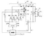
- FIG. 1 shows an equivalent circuit of a power supply device 20 and a discharge load 31 to which power is supplied from the power supply device 20 in the present embodiment.
- the inverter circuit 21 constituting the power supply device 20 converts the DC power supplied from the DC voltage source 10 into AC power, and outputs AC power to the resonant load 30 including the discharge load 31.
- the inverter circuit 21 is a push-pull inverter circuit, and includes a transformer Tr, a first switch SW1, a second switch SW2, a first diode D1, and a second diode D2.
- the transformer Tr includes a primary coil L1 and a secondary coil L2 that are magnetically coupled.
- the primary coil L1 has leakage inductances Ls1 and Ls2 at both ends thereof.
- a center tap CT is provided at the midpoint of the primary coil L1.
- the center tap CT is connected to the positive electrode of the DC voltage source 10.
- the first switch SW1 and the second switch SW2 are connected to both ends (terminals P1, P2) of the primary coil L1.
- Each of the switches SW1 and SW2 is a semiconductor switching element, specifically, an N-channel MOS-FET.
- the switches SW1 and SW2 are collectively referred to as a switch SW.
- Leakage inductances Ls1 and Ls2 exist between the drains of the switches SW1 and SW2 and the primary coil L1.
- a first diode D1 and a second diode D2 are connected in antiparallel to the first switch SW1 and the second switch SW2, respectively.
- Diodes D1 and D2 are body diodes of the switches SW1 and SW2.
- the cathodes of the diodes D1, D2 are connected to the drains of the switches SW1, SW2, and the anodes of the diodes D1, D2 are connected to the sources of the switches SW1, SW2.
- the switches SW1 and SW2 are turned on when the high drive signals gSW1 and gSW2 are input from the driver circuit 50, respectively, and are turned off when the low drive signals gSW1 and gSW2 are input. Is done.
- the AC power is output from the inverter circuit 21 by alternately turning on the first switch SW1 and the second switch SW2.
- the voltage of the DC voltage source 10 is applied to a portion between the center tap CT of the primary coil L1 and the terminal P1.
- an induced current flows upward in the drawing (from the terminal P3 to the terminal P4) with respect to the secondary coil L2.
- the second switch SW2 is turned on, the voltage of the DC voltage source 10 is applied to a portion between the center tap CT of the primary coil L1 and the terminal P2.
- an induced current flows downward in the drawing (from the terminal P4 to the terminal P3) with respect to the secondary coil L2.
- the control device 40 acquires the detected value of the input current (switch current Isw) of the inverter circuit 21 from the current sensor 41 (current detection unit), and the detected value of the output voltage (load voltage Vr) of the inverter circuit 21 from the voltage sensor 42. And the detected value of the output current (load current Ir) of the inverter circuit 21 is acquired from the current sensor 43. Based on the detection values of the sensors 41 to 43 and the required power of the discharge load 31, the drive frequency fsw of the switches SW1 and SW2 is set. Then, the control device 40 outputs a command signal corresponding to the drive frequency fsw to the driver circuit 50.
- the driver circuit 50 outputs drive signals gSW1 and gSW2 to the gates of the switches SW1 and SW2 according to the command signal.
- the discharge load 31 is an ozone generator, and two plate-like dielectric electrodes are provided with an air layer (discharge gap) interposed therebetween so as to be parallel to each other.
- a ceramic substrate is provided on the surface of the surface opposite to the air layer.
- the discharge load 31 is a “capacitive discharge load” (reactor).
- the equivalent circuit of the discharge load 31 can be expressed as a series connection body of an air layer capacitance Cg which is a capacitance of a discharge gap and a dielectric capacitance Cp which is a capacitance of a dielectric electrode.
- the characteristics of the discharge load 31 during discharge can be expressed as Zener diodes DT1, DT2 connected in parallel to the air layer capacitance Cg, having a breakdown voltage Va, and connected in opposite directions.
- the equivalent capacity C of the discharge load 31 changes according to the applied voltage.
- the equivalent capacitance C of the discharge load 31 is dominated by the air layer capacitance Cg in a region where the applied voltage is low, and is dominant in the region where the applied voltage is high.
- FIG. 2 shows the characteristics of the equivalent capacity C of the discharge load 31 with respect to the applied voltage.
- FIG. 2 shows a time change of the voltage Vb between the terminals of the discharge load 31 when the predetermined voltages Vb1 and Vb2 having a relationship of Vb1> Vb2> Va are applied to the discharge load 31.
- the inter-terminal voltage Vb increases from the time T0 and exceeds the discharge sustain voltage Va at the time T1. Thereby, barrier discharge is started from time T1. Thereafter, after the inter-terminal voltage Vb reaches the high voltage Vb1, the inter-terminal voltage Vb decreases due to discharge due to resonance. Since the inter-terminal voltage Vb is lower than the discharge sustain voltage Va at time T4, the barrier discharge is stopped at time T2. Thereafter, the inter-terminal voltage Vb becomes 0 at time T5.
- the inter-terminal voltage Vb increases from the time T0 and exceeds the discharge sustain voltage Va at the time T2. Thereby, barrier discharge is started from time T2. Thereafter, after the inter-terminal voltage Vb reaches the low voltage Vb2, the inter-terminal voltage Vb decreases due to discharge due to resonance. Since the inter-terminal voltage Vb falls below the discharge sustain voltage Va at time T3, the barrier discharge is stopped at time T3. Thereafter, the inter-terminal voltage Vb becomes 0 at time T5.
- the rise of the inter-terminal voltage Vb is slow, so when the low voltage Vb2 is applied, the start of the barrier discharge is slow (T2> T1). Further, since the apex of the inter-terminal voltage Vb is lower than when the high voltage Vb1 is applied, when the low voltage Vb2 is applied, the end of the barrier discharge is early (T4> T3). For this reason, the period during which the barrier discharge is maintained differs between when the high voltage Vb1 is applied and when the high voltage Vb1 is applied, and becomes longer when the high voltage Vb1 is applied.
- a resonant load 30 is constituted by the discharge load 31 that is a capacitive load and the leakage inductance Lsb of the coil La and the secondary coil L2 that are inductive loads.
- the resonance frequency fr of the resonance load 30 changes with the change in the equivalent capacity C of the discharge load 31 described above.
- the frequency of the current (load current Ir) flowing through the secondary coil L2 changes, and the frequency of the current flowing through the primary coil L1 (switch current Isw flowing through the switch SW) changes with the change in the frequency of the load current Ir. Change. Due to the change in the frequency fsw of the switch current Isw, a surge voltage is generated with respect to the switches SW1 and SW2, and there is a concern that the switches SW1 and SW2 may be damaged or a power loss may occur. The generation of a surge voltage accompanying the change in the frequency of the switch current Isw in the push-pull inverter circuit 21 will be described below.
- the current that flows when the first switch SW1 is in the on state is indicated by a one-dot chain line, and immediately after the first switch SW1 is turned off while the forward current is flowing to the first switch SW1.
- the flowing current is indicated by a broken line.
- FIG. 4 shows a surge voltage generated when the switch SW1 is turned off in a state in which a forward current flows through the first switch SW1.
- the switch signal Isw1 is flowing in the positive direction (for example, 10A)
- the drive signal gSW1 is changed from the high state to the low state and the first switch SW1 is turned off
- the voltage Vsw1 is applied in the steady state.
- a very high voltage (surge voltage) is generated.
- FIG. 5A shows a timing chart showing temporal changes in the load current Ir, the switch current Isw, and the drive signal gSW when the resonance frequency fr of the resonance load 30 matches the drive frequency fsw of the switch SW. .
- the load current Ir does not depend on the drive frequency fsw but changes at the resonance frequency fr.
- the switch current Isw operates at the same frequency as the load current Ir.
- the switch SW off time coincides with the time when the load current Ir crosses zero, that is, the time when the switch current Isw crosses zero, so that a surge voltage occurs in the switch SW. Absent.
- FIG. 5B shows temporal changes in the load current Ir, the switch current Isw, and the drive signal gSW when the resonance frequency fr and the drive frequency fsw are substantially equal and the resonance frequency fr is higher than the drive frequency fsw.
- a timing chart is shown. Similar to FIG. 5A, the load current Ir does not depend on the drive frequency fsw but changes at the resonance frequency fr. Further, during the ON period of the switch SW, the switch current Isw operates at the same frequency as the load current Ir. Since the resonance frequency fr is higher than the drive frequency fsw, the OFF time of the switch SW becomes later than the time when the load current Ir crosses zero, that is, the time when the switch current Isw crosses zero. For this reason, a surge voltage does not occur in the switch SW.
- FIGS. 6 to 9 show changes in the waveform of the switch current Isw when the drive frequency fsw is changed in the vicinity of the resonance frequency fr, and whether or not a surge voltage is generated.
- the OFF operation timing for the switch current Isw is changed as shown in examples (a), (b), and (c).
- the case where the drive frequency fsw is about twice the resonance frequency fr (the period of the drive signal gSW is about 1 ⁇ 2 times the switch current Isw) is taken as an example (a).
- the case where the drive frequency fsw is about 2/3 times the resonance frequency fr (the period of the drive signal gSW is about 3/2 times the switch current Isw) is taken as an example (b).
- the case where the drive frequency fsw is about 2/5 times the resonance frequency fr (the period of the drive signal gSW is about 5/2 times the switch current Isw) is taken as an example (c).
- FIG. 7 shows a timing chart showing a time change of the switch current Isw, the switch voltage Vsw, and the drive signal gSW in the example (a).
- the switch current Isw has a delayed phase with respect to the drive signal gSW.
- the switch current Isw flows in the positive direction, so that a surge voltage is generated in the switch voltage Vsw.
- FIG. 8 shows a timing chart showing the change over time of the switch current Isw, the switch voltage Vsw, and the drive signal gSW in the example (b).
- the switch current Isw has substantially the same phase and the leading phase with respect to the drive signal gSW. Since the switch current Isw flows in the negative direction when the drive signal gSW is turned off, no surge voltage is generated in the switch voltage Vsw.
- FIG. 9 shows a timing chart showing temporal changes of the switch current Isw, the switch voltage Vsw, and the drive signal gSW in the example (c).
- the switch current Isw advances and is in a phase with respect to the drive signal gSW.
- one cycle of the switch current Isw is included in half of one drive cycle (the ON period of the switch SW). That is, in the ON period of the switch SW, the switch current Isw flows in the positive direction, then flows in the negative direction, and flows again in the positive direction. Since the switch SW is turned off while the switch current Isw is flowing in the positive direction, a surge voltage is generated in the switch voltage Vsw.
- the drive frequency fsw is suppressed from becoming higher than the resonance frequency fr. To do.
- the following control is performed in order to suppress the generation of the surge voltage in a state where one cycle of the switch current Isw is included in the half cycle of the drive cycle as shown in the example (c).
- the switch SW is turned on when the drive current fsw is a negative value in a region where the drive frequency fsw is less than the lower limit frequency fm, with a predetermined lower limit frequency fm in which one half of one drive cycle is one cycle of the switch current Isw. Operate from state to off state. More specifically, the control device 40 acquires the detected value of the switch current Isw from the current sensor 41, and turns off the switch SW from the on state on condition that the detected value is a negative value (zero-crossed). Implement immediate control to manipulate the state.
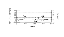
- FIG. 10 is a timing chart showing time changes of the switch current Isw, the switch voltage Vsw, and the drive signal gSW when immediate control is performed in a region where the drive frequency fsw is less than the lower limit frequency fm.
- the drive frequency fsw is about 2/5 times the resonance frequency fr, similarly to the example (c). Since the switch SW is operated from the on state to the off state on condition that the detected value of the switch current Isw is a negative value, the generation of the surge voltage in the switch voltage Vsw is suppressed.
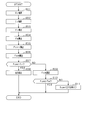
- FIG. 11 is a flowchart showing the drive frequency fsw setting process in the present embodiment. This process is performed at predetermined intervals by the control device 40.
- step S01 a detection value of the load voltage Vr applied to the resonant load 30 in one driving cycle is acquired.
- the initial value of the driving frequency fsw (driving cycle) is set within a range between a lower limit frequency fm and a resonance frequency fr that are determined from design values of the inverter circuit 21 and the resonant load 30.
- step S02 the detected value of the load current Ir flowing through the resonant load 30 in one drive cycle is acquired.
- step S03 the resonance frequency fr is calculated based on the peak value of the load voltage Vr.
- step S04 the lower limit frequency fm is calculated based on the peak value of the load voltage Vr.
- the control device 40 includes a map that associates the peak value of the load voltage Vr with the resonance frequency fr, and a map that associates the peak value of the load voltage Vr with the lower limit frequency fm. Yes.
- the control device 40 calculates the resonance frequency fr and the lower limit frequency fm using these maps.
- step S05 the output power Pout supplied to the resonant load 30 is calculated based on the detected values of the load voltage Vr and the load current Ir.
- step S06 the drive frequency fsw is calculated based on the deviation ⁇ Pout between the command value Pout * of the output power for the resonant load 30 input from the host controller to the controller 40 and the actual value of the output power Pout. To do. Specifically, for example, based on the deviation ⁇ Pout, PI control for operating the drive frequency fsw is performed.
- step S07 it is determined whether or not the advance phase of the switch current Isw with respect to the drive signal gSW is smaller than a predetermined value of 0 or more. Specifically, the drive frequency fsw is compared with the resonance frequency fr, and it is determined whether or not the drive frequency fsw is higher than an upper limit frequency obtained by subtracting a predetermined value of 0 or more from the resonance frequency fr. In the present embodiment, the resonance frequency fr is set as the upper limit frequency.
- the drive frequency fsw is higher than the upper limit frequency (S07: YES)
- step S08 the increase of the drive frequency fsw is stopped and the power output from the power supply device 20 to the resonant load 30 is prohibited.
- step S10 it is determined whether the drive frequency fsw is equal to or higher than the lower limit frequency fm. If it is determined that the drive frequency fsw is equal to or higher than the lower limit frequency fm (S10: YES), the process is terminated. If it is determined that the drive frequency fsw is less than the lower limit frequency fm (S10: NO), in step S11, the switch SW is turned off immediately on condition that the detected value of the switch current Isw is a negative value. The control is set to be performed, and the process ends.
- FIG. 12 shows the relationship between the drive frequency fsw and the output power Pout when the control of this embodiment is performed.
- the output power Pout increases as the drive frequency fsw approaches the resonance frequency fr.
- immediate control for turning off the switch SW is performed on condition that the detected value of the switch current Isw is a negative value.
- the on-time that is, the duty in one drive cycle of the switch SW (period from the on operation to the next on operation) decreases. For this reason, compared with the case where the immediate control in this embodiment is not implemented (broken line), the output power Pout is reduced.
- a push-pull inverter circuit 21 is applied.
- the number of switching elements can be reduced and the configuration can be simplified.
- production of turn-on loss can be suppressed.
- the push-pull inverter circuit 21 if a forward current flows through the switch SW and the switch SW is turned off, there is a concern that a surge voltage is generated. Therefore, when the drive frequency fsw is set so that the switch current Isw has the same phase or the leading phase with respect to the drive signal gSW, the first switch SW1 and the second switch SW2 are turned off. It is possible to suppress the surge voltage by setting the current Isw to a negative value.
- the switch current Isw is in phase with the drive signal gSW. Further, when the drive frequency fsw is increased, the switch current Isw becomes a delayed phase. That is, by setting the drive frequency fsw to be equal to or less than the resonance frequency fr, the switch current Isw can be in phase or advance with respect to the drive signal gSW.
- one cycle of the switch current Isw is included in half of the drive cycle.
- the switch current Isw oscillates between a negative value and a positive value.
- the switch current Isw has a positive value, and there is a concern that a surge voltage may be generated.
- the drive frequency fsw is less than the lower limit frequency fm, when the switch current Isw is a negative value, the generation of the surge voltage can be suppressed in advance by performing the switch SW off operation.
- one cycle of the switch current Isw can be estimated based on the voltage applied to the resonant load 30.
- the resonance frequency fr of the resonance load 30 changes while the resonance load 30 is being driven. According to the configuration of the present embodiment, even when the resonance frequency fr changes, the phase of the switch current Isw with respect to the drive signal gSW can be appropriately manipulated, and the generation of a surge voltage can be suppressed.
- the resonance frequency fr of the resonance load 30 can be set to a desired value, the control is simplified, and power loss associated with an increase in the drive frequency fsw of the switch SW can be suppressed.
- FIG. 13 is a flowchart showing the setting process of the drive frequency fsw in the second embodiment. This process is performed at predetermined intervals by the control device 40.
- the same components as those in FIG. 11 are denoted by the same reference numerals, and description thereof will be omitted as appropriate.
- the second embodiment has an electrical configuration equivalent to that of the first embodiment (FIG. 1).
- step S01 a detection value of the load voltage Vr applied to the resonant load 30 in one driving cycle is acquired.
- the detected value of the load current Ir flowing through the resonant load 30 in one drive cycle is acquired.
- step S03 the resonance frequency fr is calculated based on the peak value of the load voltage Vr.
- step S04 the lower limit frequency fm is calculated based on the peak value of the load voltage Vr.
- step S21 it is determined whether the drive frequency fsw is equal to or lower than the resonance frequency fr and equal to or higher than the lower limit frequency fm.
- the drive frequency fsw is higher than the resonance frequency fr or less than the lower limit frequency fm (S21: NO)
- step S22 the drive frequency fsw is a predetermined frequency satisfying the resonance frequency fr and the lower limit frequency fm.
- the drive frequency fsw is fixed at a predetermined frequency that satisfies the resonance frequency fr and the lower limit frequency fm.
- step S05 the drive frequency fsw is supplied to the resonance load 30 based on the detected values of the load voltage Vr and the load current Ir.
- the output power Pout is calculated.
- step S23 the intermittent ratio in the power output is set based on the output power Pout and the output power command value Pout *, and the process ends.
- FIG. 14 shows the driving signal gSW2 with the polarity reversed.
- the control device 40 according to the present embodiment turns on and off the first switch SW1 and the second switch SW2 alternately. At the time of continuous output that is not intermittent output, one of the switches SW1 and SW2 is turned on, and power is always output from the power supply device 20.
- the number of ON operations of the first switch SW1 and the second switch SW2 in a predetermined period is set while maintaining the ratio (duty) of the ON time in one drive cycle of the switches SW1 and SW2 to 50%. Decrease.
- the period of the drive cycle of the switches SW1 and SW2 ⁇ 6 is set as a predetermined period, and the number of ON operations of the first switch SW1 and the second switch SW2 is decreased from 6 times to 3 times.
- the duty is maintained at 50%, and the output power Pout is half that during continuous output.
- the switch current Isw at the time of the off operation becomes 0, and no surge voltage is generated. If the drive frequency fsw is the lower limit frequency fm at which one drive cycle of the switch SW is one cycle of the switch current Isw, the switch current Isw is 0 during the off operation, and no surge voltage is generated. Further, in a region where the drive frequency fsw is lower than the resonance frequency fr and higher than the lower limit frequency fm, the switch current Isw at the time of the off operation becomes a negative value, and no surge voltage is generated. Therefore, by setting the drive frequency fsw to a frequency range that is not less than the lower limit frequency fm and not more than the resonance frequency fr, generation of a surge voltage can be suppressed.
- the power supply device 20 is configured to intermittently output power while maintaining the drive frequency fsw in a frequency range in which no surge voltage is generated. Further, the intermittent ratio in the power output is set based on the output power Pout. As a result, desired power can be supplied to the resonant load 30. In addition, since the output is intermittently maintained while maintaining the duty at 50%, the on period of the switch SW is shortened, so that the switch current Isw becomes a negative value when the switch SW is turned off, and the surge voltage is reduced. Occurrence can be suppressed.
- the driving frequency fsw is fixed to a fixed frequency and the intermittent ratio is adjusted. Since the drive frequency fsw can be a constant value, the control can be simplified.
- the input power Pin can be calculated.
- the input power Pin of the inverter circuit 21 and the output power Pout of the inverter circuit 21 are substantially the same or have a correlation. Therefore, the output power Pout is calculated based on the input power Pin, and the output power Pout is output by setting the drive frequency fsw and the intermittent ratio based on the deviation between the output power Pout and the output power command value Pout *. It becomes possible to approach the power command value Pout *.
- the switch current Isw and the load current Ir have a proportional relationship according to the winding ratio of the transformer Tr. Furthermore, since the load current Ir and the load voltage Vr have a correlation, the resonance frequency fr and the lower limit frequency fm can be calculated based on the switch current Isw.
- the control device 40 b performs control based on the detected value of the load voltage Vr by the voltage sensor 42, that is, the detected value of the output voltage Vr output from the inverter circuit 21 to the resonant load 30. .
- the control device 40b sets the drive frequency fsw and the intermittent ratio based on the deviation between the detected value of the output voltage Vr and the output voltage command value Vr *, thereby bringing the output voltage Vr closer to the output voltage command value Vr *. It becomes possible. Further, the resonance frequency fr and the lower limit frequency fm can be calculated based on the detected value of the load voltage Vr.
- the control device 40 c performs control based on the detected value of the load current Ir by the current sensor 43, that is, the detected value of the output current Ir output from the inverter circuit 21 to the resonant load 30. .
- the control device 40c sets the drive frequency fsw and the intermittent ratio based on the deviation between the detected value of the output current Ir and the output current command value Ir *, thereby bringing the output current Ir closer to the output current command value Ir *. It becomes possible. Further, since the load current Ir and the load voltage Vr have a correlation, the resonance frequency fr and the lower limit frequency fm can be calculated based on the detected value of the load current Ir.
- the control apparatus 40 in order to suppress generation
- the detection value is acquired, and on the condition that the detection value is a negative value, an immediate control for operating the switch SW from the on state to the off state is performed. This is changed, and a voltage that changes according to the switch current Isw is detected.
- the drive frequency fsw of the drive signal gSW may be set so that the switch current Isw has the same phase or the leading phase with respect to the drive signal gSW based on the detected voltage value.
- the voltage sensor 44 may be provided between the center tap CT of the transformer Tr and the drain of the first switch SW1.
- the control device 40d acquires the detected value of the input voltage Vtr of the transformer Tr by the voltage sensor 44.
- the control device 40d can determine whether or not the switch current Isw is in the same phase or advanced phase based on the detected value of the input voltage Vtr of the transformer Tr.
- the switch current Isw is in a delayed phase, the generation of a surge voltage can be suppressed by reducing the drive frequency fsw.
- the voltage sensor may be provided between the center tap CT of the transformer Tr and the drain of the first switch SW1, and between the center tap CT of the transformer Tr and the drain of the second switch SW2. .
- the voltage sensor 45 may be provided between the input terminal and the output terminal (between the drain and source) of the first switch SW1. And it is set as the structure which the control apparatus 40e acquires the detected value of the voltage Vsw of 1st switch SW1 by the voltage sensor 45.
- FIG. The control device 40e can determine whether or not the switch current Isw is in phase or in advance based on the detected value of the voltage Vsw of the first switch SW1. When the switch current Isw is in a delayed phase, the generation of a surge voltage can be suppressed by reducing the drive frequency fsw.
- the voltage sensor may be provided between the input terminal and the output terminal of the first switch SW1 and between the input terminal and the output terminal of the second switch SW2.
- the switch voltage Vsw is sharply increased by a surge voltage and a value near 0 when the switch SW is turned off. It becomes a value near 0 again.
- the switch voltage Vsw changes from a value close to 0 to a positive value when the switch SW is turned off. That is, it is possible to determine whether or not the switch current Isw is in a leading phase with respect to the drive signal gSW based on whether or not the switch voltage Vsw is sharply increased due to the surge voltage.
- the configuration for immediately controlling the switch SW from the on state to the off state is changed. May be. That is, when the time corresponding to half of the reciprocal (1 / fm) of the lower limit frequency fm elapses after the drive signal gSW is turned on and the switch SW is turned on, one cycle of the switch current Isw elapses. The switch current Isw crosses zero and becomes a negative value. Therefore, the switch SW may be turned off when a time corresponding to the reciprocal (1 / fm) of the lower limit frequency fm has elapsed since the switch SW was turned on. In this configuration, the current sensor 41 can be omitted.
- the drive frequency fsw is compared with the resonance frequency fr as the upper limit frequency, and the switch current Isw is set to have the same phase or the leading phase with respect to the drive signal gSW.
- the detected value of the switch current Isw and the drive signal gSW are directly compared, and when the advance phase of the switch current Isw becomes less than the predetermined value, the power supply from the power supply device 20 to the resonance load 30 is supplied. It is good also as a structure which stops.
- the advance phase of the switch current Isw can be obtained as a difference between the time when the switch current Isw crosses zero and the time when the drive signal gSW is changed from the high state to the low state.
- the drive frequency fsw is fixed, but this is changed, and the drive frequency fsw is variably set in the frequency region between the lower limit frequency fm and the resonance frequency fr, and the output power Pout May be adjusted by intermittent output.
- the advance phase of the switch current Isw with respect to the drive signal becomes small and the drive frequency fsw exceeds the resonance frequency fr (upper limit frequency)
- the increase of the drive frequency fsw is stopped and the resonance load 30 from the power supply device 20 is stopped. It is preferable that the power output to be prohibited.
- the drive frequency fsw is set to a value belonging to the region below the resonance frequency fr, and the first switch SW1 and the second switch SW2 are turned off on condition that the switch current Isw is a negative value. Good.
- the resonance frequency fr is determined by the leakage inductance Lsb of the secondary coil L2 and the capacitance component of the discharge load 31.
- Switches SW1 and SW2 may be changed from N-channel MOS-FETs.
- an IGBT may be used.
- IGBT when using IGBT for switch SW1, SW2, it is good to set it as the structure which provides a free-wheeling diode.
Landscapes
- Engineering & Computer Science (AREA)
- Power Engineering (AREA)
- Inverter Devices (AREA)
Priority Applications (1)
| Application Number | Priority Date | Filing Date | Title |
|---|---|---|---|
| DE112016005137.9T DE112016005137T5 (de) | 2015-11-09 | 2016-11-02 | Leistungszuführvorrichtung |
Applications Claiming Priority (2)
| Application Number | Priority Date | Filing Date | Title |
|---|---|---|---|
| JP2015-219822 | 2015-11-09 | ||
| JP2015219822A JP6341182B2 (ja) | 2015-11-09 | 2015-11-09 | 電源装置 |
Publications (1)
| Publication Number | Publication Date |
|---|---|
| WO2017082141A1 true WO2017082141A1 (ja) | 2017-05-18 |
Family
ID=58695402
Family Applications (1)
| Application Number | Title | Priority Date | Filing Date |
|---|---|---|---|
| PCT/JP2016/082635 Ceased WO2017082141A1 (ja) | 2015-11-09 | 2016-11-02 | 電源装置 |
Country Status (3)
| Country | Link |
|---|---|
| JP (1) | JP6341182B2 (enExample) |
| DE (1) | DE112016005137T5 (enExample) |
| WO (1) | WO2017082141A1 (enExample) |
Cited By (1)
| Publication number | Priority date | Publication date | Assignee | Title |
|---|---|---|---|---|
| WO2026081394A1 (zh) * | 2024-10-18 | 2026-04-23 | 英诺赛科(珠海)科技有限公司 | 推挽逆变电路及高频电源装置 |
Families Citing this family (1)
| Publication number | Priority date | Publication date | Assignee | Title |
|---|---|---|---|---|
| US11171574B2 (en) * | 2017-07-03 | 2021-11-09 | Mitsubishi Electric Corporation | Power conversion device with estimation of load voltage based on electrostatic capacitance of load or correction coefficient |
Citations (2)
| Publication number | Priority date | Publication date | Assignee | Title |
|---|---|---|---|---|
| JP2005340185A (ja) * | 2005-04-26 | 2005-12-08 | Mitsubishi Electric Corp | プラズマ発生用電源装置の製造方法 |
| WO2008032425A1 (en) * | 2006-09-15 | 2008-03-20 | Mitsubishi Electric Corporation | Dc/dc power converting apparatus |
Family Cites Families (2)
| Publication number | Priority date | Publication date | Assignee | Title |
|---|---|---|---|---|
| JPS5681943A (en) | 1979-11-01 | 1981-07-04 | Shinkawa Ltd | Bonding device |
| JP6223907B2 (ja) | 2014-05-20 | 2017-11-01 | 日本電信電話株式会社 | ワンストップ申請システム、ワンストップ申請方法およびプログラム |
-
2015
- 2015-11-09 JP JP2015219822A patent/JP6341182B2/ja active Active
-
2016
- 2016-11-02 WO PCT/JP2016/082635 patent/WO2017082141A1/ja not_active Ceased
- 2016-11-02 DE DE112016005137.9T patent/DE112016005137T5/de not_active Withdrawn
Patent Citations (2)
| Publication number | Priority date | Publication date | Assignee | Title |
|---|---|---|---|---|
| JP2005340185A (ja) * | 2005-04-26 | 2005-12-08 | Mitsubishi Electric Corp | プラズマ発生用電源装置の製造方法 |
| WO2008032425A1 (en) * | 2006-09-15 | 2008-03-20 | Mitsubishi Electric Corporation | Dc/dc power converting apparatus |
Cited By (1)
| Publication number | Priority date | Publication date | Assignee | Title |
|---|---|---|---|---|
| WO2026081394A1 (zh) * | 2024-10-18 | 2026-04-23 | 英诺赛科(珠海)科技有限公司 | 推挽逆变电路及高频电源装置 |
Also Published As
| Publication number | Publication date |
|---|---|
| DE112016005137T5 (de) | 2018-07-26 |
| JP6341182B2 (ja) | 2018-06-13 |
| JP2017093130A (ja) | 2017-05-25 |
Similar Documents
| Publication | Publication Date | Title |
|---|---|---|
| JP6477220B2 (ja) | 共振コンバータおよびスイッチング電源装置 | |
| US8804375B2 (en) | PWM-PSM controlled power supply with auxiliary switching circuit for soft-switching | |
| US10574146B2 (en) | Converter and driving method thereof | |
| JP7325059B2 (ja) | 力率改善回路 | |
| US9787204B2 (en) | Switching power supply device | |
| US10355613B2 (en) | Switch driving circuit and switching power device using the same | |
| WO2018061286A1 (ja) | 電力変換装置 | |
| JP6313080B2 (ja) | 高周波電源装置 | |
| JP2018057223A (ja) | 高周波電源装置 | |
| KR101708482B1 (ko) | 스위치 구동 회로 및 스위치 구동 방법 | |
| JP6012822B1 (ja) | 電力変換装置 | |
| CN103715896A (zh) | 直流电源装置及其控制方法 | |
| JP2018074692A (ja) | 電力変換装置 | |
| JPWO2019202354A1 (ja) | 共振型電力変換装置の制御方法および共振型電力変換装置 | |
| JP6341182B2 (ja) | 電源装置 | |
| JP6458235B2 (ja) | スイッチング電源装置 | |
| JP6406330B2 (ja) | 電源装置 | |
| US20080037299A1 (en) | Method for driving dc-ac converter | |
| JP6756285B2 (ja) | 共振インバータ | |
| JP5169679B2 (ja) | 共振型電力変換装置 | |
| JP5962717B2 (ja) | Dc−dcコンバータ | |
| JP2006158137A (ja) | スイッチング電源装置 | |
| WO2017175722A1 (ja) | 電源装置 | |
| JP2017147892A (ja) | 共振コンバータ | |
| JP6756286B2 (ja) | 共振インバータ |
Legal Events
| Date | Code | Title | Description |
|---|---|---|---|
| 121 | Ep: the epo has been informed by wipo that ep was designated in this application |
Ref document number: 16864104 Country of ref document: EP Kind code of ref document: A1 |
|
| WWE | Wipo information: entry into national phase |
Ref document number: 112016005137 Country of ref document: DE |
|
| 122 | Ep: pct application non-entry in european phase |
Ref document number: 16864104 Country of ref document: EP Kind code of ref document: A1 |