WO2017082141A1 - 電源装置 - Google Patents
電源装置 Download PDFInfo
- Publication number
- WO2017082141A1 WO2017082141A1 PCT/JP2016/082635 JP2016082635W WO2017082141A1 WO 2017082141 A1 WO2017082141 A1 WO 2017082141A1 JP 2016082635 W JP2016082635 W JP 2016082635W WO 2017082141 A1 WO2017082141 A1 WO 2017082141A1
- Authority
- WO
- WIPO (PCT)
- Prior art keywords
- switch
- frequency
- power supply
- supply device
- current
- Prior art date
Links
Images


Classifications
-
- H—ELECTRICITY
- H02—GENERATION; CONVERSION OR DISTRIBUTION OF ELECTRIC POWER
- H02M—APPARATUS FOR CONVERSION BETWEEN AC AND AC, BETWEEN AC AND DC, OR BETWEEN DC AND DC, AND FOR USE WITH MAINS OR SIMILAR POWER SUPPLY SYSTEMS; CONVERSION OF DC OR AC INPUT POWER INTO SURGE OUTPUT POWER; CONTROL OR REGULATION THEREOF
- H02M7/00—Conversion of ac power input into dc power output; Conversion of dc power input into ac power output
- H02M7/42—Conversion of dc power input into ac power output without possibility of reversal
- H02M7/44—Conversion of dc power input into ac power output without possibility of reversal by static converters
- H02M7/48—Conversion of dc power input into ac power output without possibility of reversal by static converters using discharge tubes with control electrode or semiconductor devices with control electrode
-
- H—ELECTRICITY
- H02—GENERATION; CONVERSION OR DISTRIBUTION OF ELECTRIC POWER
- H02M—APPARATUS FOR CONVERSION BETWEEN AC AND AC, BETWEEN AC AND DC, OR BETWEEN DC AND DC, AND FOR USE WITH MAINS OR SIMILAR POWER SUPPLY SYSTEMS; CONVERSION OF DC OR AC INPUT POWER INTO SURGE OUTPUT POWER; CONTROL OR REGULATION THEREOF
- H02M1/00—Details of apparatus for conversion
- H02M1/0003—Details of control, feedback or regulation circuits
- H02M1/0032—Control circuits allowing low power mode operation, e.g. in standby mode
-
- H—ELECTRICITY
- H02—GENERATION; CONVERSION OR DISTRIBUTION OF ELECTRIC POWER
- H02M—APPARATUS FOR CONVERSION BETWEEN AC AND AC, BETWEEN AC AND DC, OR BETWEEN DC AND DC, AND FOR USE WITH MAINS OR SIMILAR POWER SUPPLY SYSTEMS; CONVERSION OF DC OR AC INPUT POWER INTO SURGE OUTPUT POWER; CONTROL OR REGULATION THEREOF
- H02M1/00—Details of apparatus for conversion
- H02M1/0048—Circuits or arrangements for reducing losses
- H02M1/0054—Transistor switching losses
- H02M1/0058—Transistor switching losses by employing soft switching techniques, i.e. commutation of transistors when applied voltage is zero or when current flow is zero
-
- H—ELECTRICITY
- H02—GENERATION; CONVERSION OR DISTRIBUTION OF ELECTRIC POWER
- H02M—APPARATUS FOR CONVERSION BETWEEN AC AND AC, BETWEEN AC AND DC, OR BETWEEN DC AND DC, AND FOR USE WITH MAINS OR SIMILAR POWER SUPPLY SYSTEMS; CONVERSION OF DC OR AC INPUT POWER INTO SURGE OUTPUT POWER; CONTROL OR REGULATION THEREOF
- H02M3/00—Conversion of dc power input into dc power output
- H02M3/01—Resonant DC/DC converters
-
- H—ELECTRICITY
- H02—GENERATION; CONVERSION OR DISTRIBUTION OF ELECTRIC POWER
- H02M—APPARATUS FOR CONVERSION BETWEEN AC AND AC, BETWEEN AC AND DC, OR BETWEEN DC AND DC, AND FOR USE WITH MAINS OR SIMILAR POWER SUPPLY SYSTEMS; CONVERSION OF DC OR AC INPUT POWER INTO SURGE OUTPUT POWER; CONTROL OR REGULATION THEREOF
- H02M3/00—Conversion of dc power input into dc power output
- H02M3/22—Conversion of dc power input into dc power output with intermediate conversion into ac
- H02M3/24—Conversion of dc power input into dc power output with intermediate conversion into ac by static converters
- H02M3/28—Conversion of dc power input into dc power output with intermediate conversion into ac by static converters using discharge tubes with control electrode or semiconductor devices with control electrode to produce the intermediate ac
- H02M3/325—Conversion of dc power input into dc power output with intermediate conversion into ac by static converters using discharge tubes with control electrode or semiconductor devices with control electrode to produce the intermediate ac using devices of a triode or a transistor type requiring continuous application of a control signal
- H02M3/335—Conversion of dc power input into dc power output with intermediate conversion into ac by static converters using discharge tubes with control electrode or semiconductor devices with control electrode to produce the intermediate ac using devices of a triode or a transistor type requiring continuous application of a control signal using semiconductor devices only
- H02M3/33569—Conversion of dc power input into dc power output with intermediate conversion into ac by static converters using discharge tubes with control electrode or semiconductor devices with control electrode to produce the intermediate ac using devices of a triode or a transistor type requiring continuous application of a control signal using semiconductor devices only having several active switching elements
- H02M3/33571—Half-bridge at primary side of an isolation transformer
-
- H—ELECTRICITY
- H02—GENERATION; CONVERSION OR DISTRIBUTION OF ELECTRIC POWER
- H02M—APPARATUS FOR CONVERSION BETWEEN AC AND AC, BETWEEN AC AND DC, OR BETWEEN DC AND DC, AND FOR USE WITH MAINS OR SIMILAR POWER SUPPLY SYSTEMS; CONVERSION OF DC OR AC INPUT POWER INTO SURGE OUTPUT POWER; CONTROL OR REGULATION THEREOF
- H02M3/00—Conversion of dc power input into dc power output
- H02M3/22—Conversion of dc power input into dc power output with intermediate conversion into ac
- H02M3/24—Conversion of dc power input into dc power output with intermediate conversion into ac by static converters
- H02M3/28—Conversion of dc power input into dc power output with intermediate conversion into ac by static converters using discharge tubes with control electrode or semiconductor devices with control electrode to produce the intermediate ac
- H02M3/325—Conversion of dc power input into dc power output with intermediate conversion into ac by static converters using discharge tubes with control electrode or semiconductor devices with control electrode to produce the intermediate ac using devices of a triode or a transistor type requiring continuous application of a control signal
- H02M3/335—Conversion of dc power input into dc power output with intermediate conversion into ac by static converters using discharge tubes with control electrode or semiconductor devices with control electrode to produce the intermediate ac using devices of a triode or a transistor type requiring continuous application of a control signal using semiconductor devices only
- H02M3/33569—Conversion of dc power input into dc power output with intermediate conversion into ac by static converters using discharge tubes with control electrode or semiconductor devices with control electrode to produce the intermediate ac using devices of a triode or a transistor type requiring continuous application of a control signal using semiconductor devices only having several active switching elements
- H02M3/33573—Full-bridge at primary side of an isolation transformer
-
- H—ELECTRICITY
- H02—GENERATION; CONVERSION OR DISTRIBUTION OF ELECTRIC POWER
- H02M—APPARATUS FOR CONVERSION BETWEEN AC AND AC, BETWEEN AC AND DC, OR BETWEEN DC AND DC, AND FOR USE WITH MAINS OR SIMILAR POWER SUPPLY SYSTEMS; CONVERSION OF DC OR AC INPUT POWER INTO SURGE OUTPUT POWER; CONTROL OR REGULATION THEREOF
- H02M3/00—Conversion of dc power input into dc power output
- H02M3/22—Conversion of dc power input into dc power output with intermediate conversion into ac
- H02M3/24—Conversion of dc power input into dc power output with intermediate conversion into ac by static converters
- H02M3/28—Conversion of dc power input into dc power output with intermediate conversion into ac by static converters using discharge tubes with control electrode or semiconductor devices with control electrode to produce the intermediate ac
- H02M3/325—Conversion of dc power input into dc power output with intermediate conversion into ac by static converters using discharge tubes with control electrode or semiconductor devices with control electrode to produce the intermediate ac using devices of a triode or a transistor type requiring continuous application of a control signal
- H02M3/335—Conversion of dc power input into dc power output with intermediate conversion into ac by static converters using discharge tubes with control electrode or semiconductor devices with control electrode to produce the intermediate ac using devices of a triode or a transistor type requiring continuous application of a control signal using semiconductor devices only
- H02M3/337—Conversion of dc power input into dc power output with intermediate conversion into ac by static converters using discharge tubes with control electrode or semiconductor devices with control electrode to produce the intermediate ac using devices of a triode or a transistor type requiring continuous application of a control signal using semiconductor devices only in push-pull configuration
- H02M3/3376—Conversion of dc power input into dc power output with intermediate conversion into ac by static converters using discharge tubes with control electrode or semiconductor devices with control electrode to produce the intermediate ac using devices of a triode or a transistor type requiring continuous application of a control signal using semiconductor devices only in push-pull configuration with automatic control of output voltage or current
-
- H—ELECTRICITY
- H02—GENERATION; CONVERSION OR DISTRIBUTION OF ELECTRIC POWER
- H02M—APPARATUS FOR CONVERSION BETWEEN AC AND AC, BETWEEN AC AND DC, OR BETWEEN DC AND DC, AND FOR USE WITH MAINS OR SIMILAR POWER SUPPLY SYSTEMS; CONVERSION OF DC OR AC INPUT POWER INTO SURGE OUTPUT POWER; CONTROL OR REGULATION THEREOF
- H02M7/00—Conversion of ac power input into dc power output; Conversion of dc power input into ac power output
- H02M7/42—Conversion of dc power input into ac power output without possibility of reversal
- H02M7/44—Conversion of dc power input into ac power output without possibility of reversal by static converters
- H02M7/48—Conversion of dc power input into ac power output without possibility of reversal by static converters using discharge tubes with control electrode or semiconductor devices with control electrode
- H02M7/4815—Resonant converters
-
- H—ELECTRICITY
- H02—GENERATION; CONVERSION OR DISTRIBUTION OF ELECTRIC POWER
- H02M—APPARATUS FOR CONVERSION BETWEEN AC AND AC, BETWEEN AC AND DC, OR BETWEEN DC AND DC, AND FOR USE WITH MAINS OR SIMILAR POWER SUPPLY SYSTEMS; CONVERSION OF DC OR AC INPUT POWER INTO SURGE OUTPUT POWER; CONTROL OR REGULATION THEREOF
- H02M7/00—Conversion of ac power input into dc power output; Conversion of dc power input into ac power output
- H02M7/42—Conversion of dc power input into ac power output without possibility of reversal
- H02M7/44—Conversion of dc power input into ac power output without possibility of reversal by static converters
- H02M7/48—Conversion of dc power input into ac power output without possibility of reversal by static converters using discharge tubes with control electrode or semiconductor devices with control electrode
- H02M7/53—Conversion of dc power input into ac power output without possibility of reversal by static converters using discharge tubes with control electrode or semiconductor devices with control electrode using devices of a triode or transistor type requiring continuous application of a control signal
- H02M7/537—Conversion of dc power input into ac power output without possibility of reversal by static converters using discharge tubes with control electrode or semiconductor devices with control electrode using devices of a triode or transistor type requiring continuous application of a control signal using semiconductor devices only, e.g. single switched pulse inverters
- H02M7/538—Conversion of dc power input into ac power output without possibility of reversal by static converters using discharge tubes with control electrode or semiconductor devices with control electrode using devices of a triode or transistor type requiring continuous application of a control signal using semiconductor devices only, e.g. single switched pulse inverters in a push-pull configuration
-
- Y—GENERAL TAGGING OF NEW TECHNOLOGICAL DEVELOPMENTS; GENERAL TAGGING OF CROSS-SECTIONAL TECHNOLOGIES SPANNING OVER SEVERAL SECTIONS OF THE IPC; TECHNICAL SUBJECTS COVERED BY FORMER USPC CROSS-REFERENCE ART COLLECTIONS [XRACs] AND DIGESTS
- Y02—TECHNOLOGIES OR APPLICATIONS FOR MITIGATION OR ADAPTATION AGAINST CLIMATE CHANGE
- Y02B—CLIMATE CHANGE MITIGATION TECHNOLOGIES RELATED TO BUILDINGS, e.g. HOUSING, HOUSE APPLIANCES OR RELATED END-USER APPLICATIONS
- Y02B70/00—Technologies for an efficient end-user side electric power management and consumption
- Y02B70/10—Technologies improving the efficiency by using switched-mode power supplies [SMPS], i.e. efficient power electronics conversion e.g. power factor correction or reduction of losses in power supplies or efficient standby modes
Definitions
- the present invention relates to a power supply device having an inverter circuit that is supplied with DC power from a DC voltage source and outputs AC power to a resonant load having series resonance characteristics.
- a resonant load including an ozone generator, a plasma processing apparatus, and the like operates by receiving high-frequency power from a high-frequency power supply.
- a high-frequency power supply device that supplies power to an ozone generator or the like is supplied with DC power from a DC power source and performs voltage adjustment, and DC power is supplied from the DCDC converter to perform DC-AC conversion.
- an inverter circuit to be implemented.
- the impedance when the resonant load side is viewed from the high frequency power supply device may change.
- the equivalent capacity of the discharge load that constitutes the ozone generator changes according to the applied voltage.
- the impedance of the resonant load changes when an abnormal discharge accompanied by the generation of an arc occurs during the plasma processing.
- the frequency of the output voltage of the inverter circuit is changed to keep the phase of the output current in a delayed phase, and the amplitude of the output voltage of the DCDC converter is changed to reduce the power loss.
- Patent Document 1 A method for suppressing the deterioration is described in Patent Document 1.
- the present disclosure has been made in view of the above-described problem, and mainly applies a push-pull type inverter and suppresses generation of a surge voltage in a power supply device that outputs AC power to a resonant load. Objective.
- the configuration of the present disclosure is a power supply device that includes an inverter circuit that is supplied with DC power from a DC voltage source and outputs AC power to a resonant load having series resonance characteristics, and the inverter circuit includes a center tap.
- a transformer having a primary coil and a secondary coil magnetically coupled to the primary coil; a first switch and a second switch which are semiconductor switching elements connected to both ends of the primary coil;
- a push-pull type inverter circuit having a switch and a first diode and a second diode connected in antiparallel to the second switch, respectively, for a drive signal for driving the first switch and the second switch
- the switch currents flowing through the first switch and the second switch are in phase or lead phase.
- a control device for setting the drive frequency of the drive signal.
- FIG. 1 is a diagram illustrating an electrical configuration of the first embodiment.
- FIG. 2 is a diagram showing a change in the capacity of the capacitive discharge load.
- FIG. 3 is a diagram showing a current flow when a surge voltage is generated.
- FIG. 4 is a timing chart showing the change over time of the switch voltage, the switch current, and the drive signal when a surge voltage occurs.
- FIG. 5 is a timing chart showing changes in load current, switch current, and drive signal over time when the switch current is in the same phase and leading phase with respect to the drive signal.
- FIG. 6 is a diagram illustrating an example of the OFF operation timing with respect to the switch current.
- FIG. 7 is a timing chart showing the time variation of the switch voltage, the switch current, and the drive signal when the switch current is in a lagging phase.
- FIG. 8 is a timing chart showing the time variation of the switch voltage, the switch current, and the drive signal when the switch current is in the lead phase and no surge voltage is generated
- FIG. 9 is a timing chart showing the time variation of the switch voltage, the switch current, and the drive signal when the switch current is in the lead phase and the surge voltage is generated.
- FIG. 10 is a timing chart showing temporal changes in the switch voltage, the switch current, and the drive signal when the control in the first embodiment is performed.
- FIG. 11 is a timing chart showing a drive frequency setting process in the first embodiment.
- FIG. 12 is a diagram illustrating the relationship between the drive frequency and the output power when the control according to the first embodiment is performed.
- FIG. 13 is a timing chart showing a drive frequency setting process in the second embodiment.
- FIG. 14 is a diagram illustrating intermittent processing in the second embodiment.
- FIG. 15 is a diagram illustrating an electrical configuration in a modified example
- FIG. 16 is a diagram illustrating an electrical configuration in a modified example.
- FIG. 17 is a diagram illustrating an electrical configuration in a modified example.
- FIG. 18 is a diagram illustrating an electrical configuration in a modified example.
- FIG. 19 is a timing chart showing temporal changes in the switch current, the transformer voltage, and the gate voltage when the switch current is in a lagging phase.
- FIG. 19 is a timing chart showing temporal changes in the switch current, the transformer voltage, and the gate voltage when the switch current is in a lagging phase.
- FIG. 20 is a timing chart showing temporal changes in the switch current, the transformer voltage, and the gate voltage when the switch current is in the lead phase and no surge voltage occurs.
- FIG. 21 is a diagram illustrating an electrical configuration in a modified example.
- FIG. 22 is a timing chart showing temporal changes of the switch voltage, the switch current, and the gate voltage when the switch current is in a lagging phase.
- FIG. 23 is a timing chart showing temporal changes in the switch voltage, the switch current, and the gate voltage when the switch current is in the lead phase and no surge voltage is generated.
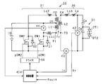
- FIG. 1 shows an equivalent circuit of a power supply device 20 and a discharge load 31 to which power is supplied from the power supply device 20 in the present embodiment.
- the inverter circuit 21 constituting the power supply device 20 converts the DC power supplied from the DC voltage source 10 into AC power, and outputs AC power to the resonant load 30 including the discharge load 31.
- the inverter circuit 21 is a push-pull inverter circuit, and includes a transformer Tr, a first switch SW1, a second switch SW2, a first diode D1, and a second diode D2.
- the transformer Tr includes a primary coil L1 and a secondary coil L2 that are magnetically coupled.
- the primary coil L1 has leakage inductances Ls1 and Ls2 at both ends thereof.
- a center tap CT is provided at the midpoint of the primary coil L1.
- the center tap CT is connected to the positive electrode of the DC voltage source 10.
- the first switch SW1 and the second switch SW2 are connected to both ends (terminals P1, P2) of the primary coil L1.
- Each of the switches SW1 and SW2 is a semiconductor switching element, specifically, an N-channel MOS-FET.
- the switches SW1 and SW2 are collectively referred to as a switch SW.
- Leakage inductances Ls1 and Ls2 exist between the drains of the switches SW1 and SW2 and the primary coil L1.
- a first diode D1 and a second diode D2 are connected in antiparallel to the first switch SW1 and the second switch SW2, respectively.
- Diodes D1 and D2 are body diodes of the switches SW1 and SW2.
- the cathodes of the diodes D1, D2 are connected to the drains of the switches SW1, SW2, and the anodes of the diodes D1, D2 are connected to the sources of the switches SW1, SW2.
- the switches SW1 and SW2 are turned on when the high drive signals gSW1 and gSW2 are input from the driver circuit 50, respectively, and are turned off when the low drive signals gSW1 and gSW2 are input. Is done.
- the AC power is output from the inverter circuit 21 by alternately turning on the first switch SW1 and the second switch SW2.
- the voltage of the DC voltage source 10 is applied to a portion between the center tap CT of the primary coil L1 and the terminal P1.
- an induced current flows upward in the drawing (from the terminal P3 to the terminal P4) with respect to the secondary coil L2.
- the second switch SW2 is turned on, the voltage of the DC voltage source 10 is applied to a portion between the center tap CT of the primary coil L1 and the terminal P2.
- an induced current flows downward in the drawing (from the terminal P4 to the terminal P3) with respect to the secondary coil L2.
- the control device 40 acquires the detected value of the input current (switch current Isw) of the inverter circuit 21 from the current sensor 41 (current detection unit), and the detected value of the output voltage (load voltage Vr) of the inverter circuit 21 from the voltage sensor 42. And the detected value of the output current (load current Ir) of the inverter circuit 21 is acquired from the current sensor 43. Based on the detection values of the sensors 41 to 43 and the required power of the discharge load 31, the drive frequency fsw of the switches SW1 and SW2 is set. Then, the control device 40 outputs a command signal corresponding to the drive frequency fsw to the driver circuit 50.
- the driver circuit 50 outputs drive signals gSW1 and gSW2 to the gates of the switches SW1 and SW2 according to the command signal.
- the discharge load 31 is an ozone generator, and two plate-like dielectric electrodes are provided with an air layer (discharge gap) interposed therebetween so as to be parallel to each other.
- a ceramic substrate is provided on the surface of the surface opposite to the air layer.
- the discharge load 31 is a “capacitive discharge load” (reactor).
- the equivalent circuit of the discharge load 31 can be expressed as a series connection body of an air layer capacitance Cg which is a capacitance of a discharge gap and a dielectric capacitance Cp which is a capacitance of a dielectric electrode.
- the characteristics of the discharge load 31 during discharge can be expressed as Zener diodes DT1, DT2 connected in parallel to the air layer capacitance Cg, having a breakdown voltage Va, and connected in opposite directions.
- the equivalent capacity C of the discharge load 31 changes according to the applied voltage.
- the equivalent capacitance C of the discharge load 31 is dominated by the air layer capacitance Cg in a region where the applied voltage is low, and is dominant in the region where the applied voltage is high.
- FIG. 2 shows the characteristics of the equivalent capacity C of the discharge load 31 with respect to the applied voltage.
- FIG. 2 shows a time change of the voltage Vb between the terminals of the discharge load 31 when the predetermined voltages Vb1 and Vb2 having a relationship of Vb1> Vb2> Va are applied to the discharge load 31.
- the inter-terminal voltage Vb increases from the time T0 and exceeds the discharge sustain voltage Va at the time T1. Thereby, barrier discharge is started from time T1. Thereafter, after the inter-terminal voltage Vb reaches the high voltage Vb1, the inter-terminal voltage Vb decreases due to discharge due to resonance. Since the inter-terminal voltage Vb is lower than the discharge sustain voltage Va at time T4, the barrier discharge is stopped at time T2. Thereafter, the inter-terminal voltage Vb becomes 0 at time T5.
- the inter-terminal voltage Vb increases from the time T0 and exceeds the discharge sustain voltage Va at the time T2. Thereby, barrier discharge is started from time T2. Thereafter, after the inter-terminal voltage Vb reaches the low voltage Vb2, the inter-terminal voltage Vb decreases due to discharge due to resonance. Since the inter-terminal voltage Vb falls below the discharge sustain voltage Va at time T3, the barrier discharge is stopped at time T3. Thereafter, the inter-terminal voltage Vb becomes 0 at time T5.
- the rise of the inter-terminal voltage Vb is slow, so when the low voltage Vb2 is applied, the start of the barrier discharge is slow (T2> T1). Further, since the apex of the inter-terminal voltage Vb is lower than when the high voltage Vb1 is applied, when the low voltage Vb2 is applied, the end of the barrier discharge is early (T4> T3). For this reason, the period during which the barrier discharge is maintained differs between when the high voltage Vb1 is applied and when the high voltage Vb1 is applied, and becomes longer when the high voltage Vb1 is applied.
- a resonant load 30 is constituted by the discharge load 31 that is a capacitive load and the leakage inductance Lsb of the coil La and the secondary coil L2 that are inductive loads.
- the resonance frequency fr of the resonance load 30 changes with the change in the equivalent capacity C of the discharge load 31 described above.
- the frequency of the current (load current Ir) flowing through the secondary coil L2 changes, and the frequency of the current flowing through the primary coil L1 (switch current Isw flowing through the switch SW) changes with the change in the frequency of the load current Ir. Change. Due to the change in the frequency fsw of the switch current Isw, a surge voltage is generated with respect to the switches SW1 and SW2, and there is a concern that the switches SW1 and SW2 may be damaged or a power loss may occur. The generation of a surge voltage accompanying the change in the frequency of the switch current Isw in the push-pull inverter circuit 21 will be described below.
- the current that flows when the first switch SW1 is in the on state is indicated by a one-dot chain line, and immediately after the first switch SW1 is turned off while the forward current is flowing to the first switch SW1.
- the flowing current is indicated by a broken line.
- FIG. 4 shows a surge voltage generated when the switch SW1 is turned off in a state in which a forward current flows through the first switch SW1.
- the switch signal Isw1 is flowing in the positive direction (for example, 10A)
- the drive signal gSW1 is changed from the high state to the low state and the first switch SW1 is turned off
- the voltage Vsw1 is applied in the steady state.
- a very high voltage (surge voltage) is generated.
- FIG. 5A shows a timing chart showing temporal changes in the load current Ir, the switch current Isw, and the drive signal gSW when the resonance frequency fr of the resonance load 30 matches the drive frequency fsw of the switch SW. .
- the load current Ir does not depend on the drive frequency fsw but changes at the resonance frequency fr.
- the switch current Isw operates at the same frequency as the load current Ir.
- the switch SW off time coincides with the time when the load current Ir crosses zero, that is, the time when the switch current Isw crosses zero, so that a surge voltage occurs in the switch SW. Absent.
- FIG. 5B shows temporal changes in the load current Ir, the switch current Isw, and the drive signal gSW when the resonance frequency fr and the drive frequency fsw are substantially equal and the resonance frequency fr is higher than the drive frequency fsw.
- a timing chart is shown. Similar to FIG. 5A, the load current Ir does not depend on the drive frequency fsw but changes at the resonance frequency fr. Further, during the ON period of the switch SW, the switch current Isw operates at the same frequency as the load current Ir. Since the resonance frequency fr is higher than the drive frequency fsw, the OFF time of the switch SW becomes later than the time when the load current Ir crosses zero, that is, the time when the switch current Isw crosses zero. For this reason, a surge voltage does not occur in the switch SW.
- FIGS. 6 to 9 show changes in the waveform of the switch current Isw when the drive frequency fsw is changed in the vicinity of the resonance frequency fr, and whether or not a surge voltage is generated.
- the OFF operation timing for the switch current Isw is changed as shown in examples (a), (b), and (c).
- the case where the drive frequency fsw is about twice the resonance frequency fr (the period of the drive signal gSW is about 1 ⁇ 2 times the switch current Isw) is taken as an example (a).
- the case where the drive frequency fsw is about 2/3 times the resonance frequency fr (the period of the drive signal gSW is about 3/2 times the switch current Isw) is taken as an example (b).
- the case where the drive frequency fsw is about 2/5 times the resonance frequency fr (the period of the drive signal gSW is about 5/2 times the switch current Isw) is taken as an example (c).
- FIG. 7 shows a timing chart showing a time change of the switch current Isw, the switch voltage Vsw, and the drive signal gSW in the example (a).
- the switch current Isw has a delayed phase with respect to the drive signal gSW.
- the switch current Isw flows in the positive direction, so that a surge voltage is generated in the switch voltage Vsw.
- FIG. 8 shows a timing chart showing the change over time of the switch current Isw, the switch voltage Vsw, and the drive signal gSW in the example (b).
- the switch current Isw has substantially the same phase and the leading phase with respect to the drive signal gSW. Since the switch current Isw flows in the negative direction when the drive signal gSW is turned off, no surge voltage is generated in the switch voltage Vsw.
- FIG. 9 shows a timing chart showing temporal changes of the switch current Isw, the switch voltage Vsw, and the drive signal gSW in the example (c).
- the switch current Isw advances and is in a phase with respect to the drive signal gSW.
- one cycle of the switch current Isw is included in half of one drive cycle (the ON period of the switch SW). That is, in the ON period of the switch SW, the switch current Isw flows in the positive direction, then flows in the negative direction, and flows again in the positive direction. Since the switch SW is turned off while the switch current Isw is flowing in the positive direction, a surge voltage is generated in the switch voltage Vsw.
- the drive frequency fsw is suppressed from becoming higher than the resonance frequency fr. To do.
- the following control is performed in order to suppress the generation of the surge voltage in a state where one cycle of the switch current Isw is included in the half cycle of the drive cycle as shown in the example (c).
- the switch SW is turned on when the drive current fsw is a negative value in a region where the drive frequency fsw is less than the lower limit frequency fm, with a predetermined lower limit frequency fm in which one half of one drive cycle is one cycle of the switch current Isw. Operate from state to off state. More specifically, the control device 40 acquires the detected value of the switch current Isw from the current sensor 41, and turns off the switch SW from the on state on condition that the detected value is a negative value (zero-crossed). Implement immediate control to manipulate the state.
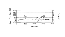
- FIG. 10 is a timing chart showing time changes of the switch current Isw, the switch voltage Vsw, and the drive signal gSW when immediate control is performed in a region where the drive frequency fsw is less than the lower limit frequency fm.
- the drive frequency fsw is about 2/5 times the resonance frequency fr, similarly to the example (c). Since the switch SW is operated from the on state to the off state on condition that the detected value of the switch current Isw is a negative value, the generation of the surge voltage in the switch voltage Vsw is suppressed.
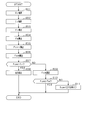
- FIG. 11 is a flowchart showing the drive frequency fsw setting process in the present embodiment. This process is performed at predetermined intervals by the control device 40.
- step S01 a detection value of the load voltage Vr applied to the resonant load 30 in one driving cycle is acquired.
- the initial value of the driving frequency fsw (driving cycle) is set within a range between a lower limit frequency fm and a resonance frequency fr that are determined from design values of the inverter circuit 21 and the resonant load 30.
- step S02 the detected value of the load current Ir flowing through the resonant load 30 in one drive cycle is acquired.
- step S03 the resonance frequency fr is calculated based on the peak value of the load voltage Vr.
- step S04 the lower limit frequency fm is calculated based on the peak value of the load voltage Vr.
- the control device 40 includes a map that associates the peak value of the load voltage Vr with the resonance frequency fr, and a map that associates the peak value of the load voltage Vr with the lower limit frequency fm. Yes.
- the control device 40 calculates the resonance frequency fr and the lower limit frequency fm using these maps.
- step S05 the output power Pout supplied to the resonant load 30 is calculated based on the detected values of the load voltage Vr and the load current Ir.
- step S06 the drive frequency fsw is calculated based on the deviation ⁇ Pout between the command value Pout * of the output power for the resonant load 30 input from the host controller to the controller 40 and the actual value of the output power Pout. To do. Specifically, for example, based on the deviation ⁇ Pout, PI control for operating the drive frequency fsw is performed.
- step S07 it is determined whether or not the advance phase of the switch current Isw with respect to the drive signal gSW is smaller than a predetermined value of 0 or more. Specifically, the drive frequency fsw is compared with the resonance frequency fr, and it is determined whether or not the drive frequency fsw is higher than an upper limit frequency obtained by subtracting a predetermined value of 0 or more from the resonance frequency fr. In the present embodiment, the resonance frequency fr is set as the upper limit frequency.
- the drive frequency fsw is higher than the upper limit frequency (S07: YES)
- step S08 the increase of the drive frequency fsw is stopped and the power output from the power supply device 20 to the resonant load 30 is prohibited.
- step S10 it is determined whether the drive frequency fsw is equal to or higher than the lower limit frequency fm. If it is determined that the drive frequency fsw is equal to or higher than the lower limit frequency fm (S10: YES), the process is terminated. If it is determined that the drive frequency fsw is less than the lower limit frequency fm (S10: NO), in step S11, the switch SW is turned off immediately on condition that the detected value of the switch current Isw is a negative value. The control is set to be performed, and the process ends.
- FIG. 12 shows the relationship between the drive frequency fsw and the output power Pout when the control of this embodiment is performed.
- the output power Pout increases as the drive frequency fsw approaches the resonance frequency fr.
- immediate control for turning off the switch SW is performed on condition that the detected value of the switch current Isw is a negative value.
- the on-time that is, the duty in one drive cycle of the switch SW (period from the on operation to the next on operation) decreases. For this reason, compared with the case where the immediate control in this embodiment is not implemented (broken line), the output power Pout is reduced.
- a push-pull inverter circuit 21 is applied.
- the number of switching elements can be reduced and the configuration can be simplified.
- production of turn-on loss can be suppressed.
- the push-pull inverter circuit 21 if a forward current flows through the switch SW and the switch SW is turned off, there is a concern that a surge voltage is generated. Therefore, when the drive frequency fsw is set so that the switch current Isw has the same phase or the leading phase with respect to the drive signal gSW, the first switch SW1 and the second switch SW2 are turned off. It is possible to suppress the surge voltage by setting the current Isw to a negative value.
- the switch current Isw is in phase with the drive signal gSW. Further, when the drive frequency fsw is increased, the switch current Isw becomes a delayed phase. That is, by setting the drive frequency fsw to be equal to or less than the resonance frequency fr, the switch current Isw can be in phase or advance with respect to the drive signal gSW.
- one cycle of the switch current Isw is included in half of the drive cycle.
- the switch current Isw oscillates between a negative value and a positive value.
- the switch current Isw has a positive value, and there is a concern that a surge voltage may be generated.
- the drive frequency fsw is less than the lower limit frequency fm, when the switch current Isw is a negative value, the generation of the surge voltage can be suppressed in advance by performing the switch SW off operation.
- one cycle of the switch current Isw can be estimated based on the voltage applied to the resonant load 30.
- the resonance frequency fr of the resonance load 30 changes while the resonance load 30 is being driven. According to the configuration of the present embodiment, even when the resonance frequency fr changes, the phase of the switch current Isw with respect to the drive signal gSW can be appropriately manipulated, and the generation of a surge voltage can be suppressed.
- the resonance frequency fr of the resonance load 30 can be set to a desired value, the control is simplified, and power loss associated with an increase in the drive frequency fsw of the switch SW can be suppressed.
- FIG. 13 is a flowchart showing the setting process of the drive frequency fsw in the second embodiment. This process is performed at predetermined intervals by the control device 40.
- the same components as those in FIG. 11 are denoted by the same reference numerals, and description thereof will be omitted as appropriate.
- the second embodiment has an electrical configuration equivalent to that of the first embodiment (FIG. 1).
- step S01 a detection value of the load voltage Vr applied to the resonant load 30 in one driving cycle is acquired.
- the detected value of the load current Ir flowing through the resonant load 30 in one drive cycle is acquired.
- step S03 the resonance frequency fr is calculated based on the peak value of the load voltage Vr.
- step S04 the lower limit frequency fm is calculated based on the peak value of the load voltage Vr.
- step S21 it is determined whether the drive frequency fsw is equal to or lower than the resonance frequency fr and equal to or higher than the lower limit frequency fm.
- the drive frequency fsw is higher than the resonance frequency fr or less than the lower limit frequency fm (S21: NO)
- step S22 the drive frequency fsw is a predetermined frequency satisfying the resonance frequency fr and the lower limit frequency fm.
- the drive frequency fsw is fixed at a predetermined frequency that satisfies the resonance frequency fr and the lower limit frequency fm.
- step S05 the drive frequency fsw is supplied to the resonance load 30 based on the detected values of the load voltage Vr and the load current Ir.
- the output power Pout is calculated.
- step S23 the intermittent ratio in the power output is set based on the output power Pout and the output power command value Pout *, and the process ends.
- FIG. 14 shows the driving signal gSW2 with the polarity reversed.
- the control device 40 according to the present embodiment turns on and off the first switch SW1 and the second switch SW2 alternately. At the time of continuous output that is not intermittent output, one of the switches SW1 and SW2 is turned on, and power is always output from the power supply device 20.
- the number of ON operations of the first switch SW1 and the second switch SW2 in a predetermined period is set while maintaining the ratio (duty) of the ON time in one drive cycle of the switches SW1 and SW2 to 50%. Decrease.
- the period of the drive cycle of the switches SW1 and SW2 ⁇ 6 is set as a predetermined period, and the number of ON operations of the first switch SW1 and the second switch SW2 is decreased from 6 times to 3 times.
- the duty is maintained at 50%, and the output power Pout is half that during continuous output.
- the switch current Isw at the time of the off operation becomes 0, and no surge voltage is generated. If the drive frequency fsw is the lower limit frequency fm at which one drive cycle of the switch SW is one cycle of the switch current Isw, the switch current Isw is 0 during the off operation, and no surge voltage is generated. Further, in a region where the drive frequency fsw is lower than the resonance frequency fr and higher than the lower limit frequency fm, the switch current Isw at the time of the off operation becomes a negative value, and no surge voltage is generated. Therefore, by setting the drive frequency fsw to a frequency range that is not less than the lower limit frequency fm and not more than the resonance frequency fr, generation of a surge voltage can be suppressed.
- the power supply device 20 is configured to intermittently output power while maintaining the drive frequency fsw in a frequency range in which no surge voltage is generated. Further, the intermittent ratio in the power output is set based on the output power Pout. As a result, desired power can be supplied to the resonant load 30. In addition, since the output is intermittently maintained while maintaining the duty at 50%, the on period of the switch SW is shortened, so that the switch current Isw becomes a negative value when the switch SW is turned off, and the surge voltage is reduced. Occurrence can be suppressed.
- the driving frequency fsw is fixed to a fixed frequency and the intermittent ratio is adjusted. Since the drive frequency fsw can be a constant value, the control can be simplified.
- the input power Pin can be calculated.
- the input power Pin of the inverter circuit 21 and the output power Pout of the inverter circuit 21 are substantially the same or have a correlation. Therefore, the output power Pout is calculated based on the input power Pin, and the output power Pout is output by setting the drive frequency fsw and the intermittent ratio based on the deviation between the output power Pout and the output power command value Pout *. It becomes possible to approach the power command value Pout *.
- the switch current Isw and the load current Ir have a proportional relationship according to the winding ratio of the transformer Tr. Furthermore, since the load current Ir and the load voltage Vr have a correlation, the resonance frequency fr and the lower limit frequency fm can be calculated based on the switch current Isw.
- the control device 40 b performs control based on the detected value of the load voltage Vr by the voltage sensor 42, that is, the detected value of the output voltage Vr output from the inverter circuit 21 to the resonant load 30. .
- the control device 40b sets the drive frequency fsw and the intermittent ratio based on the deviation between the detected value of the output voltage Vr and the output voltage command value Vr *, thereby bringing the output voltage Vr closer to the output voltage command value Vr *. It becomes possible. Further, the resonance frequency fr and the lower limit frequency fm can be calculated based on the detected value of the load voltage Vr.
- the control device 40 c performs control based on the detected value of the load current Ir by the current sensor 43, that is, the detected value of the output current Ir output from the inverter circuit 21 to the resonant load 30. .
- the control device 40c sets the drive frequency fsw and the intermittent ratio based on the deviation between the detected value of the output current Ir and the output current command value Ir *, thereby bringing the output current Ir closer to the output current command value Ir *. It becomes possible. Further, since the load current Ir and the load voltage Vr have a correlation, the resonance frequency fr and the lower limit frequency fm can be calculated based on the detected value of the load current Ir.
- the control apparatus 40 in order to suppress generation
- the detection value is acquired, and on the condition that the detection value is a negative value, an immediate control for operating the switch SW from the on state to the off state is performed. This is changed, and a voltage that changes according to the switch current Isw is detected.
- the drive frequency fsw of the drive signal gSW may be set so that the switch current Isw has the same phase or the leading phase with respect to the drive signal gSW based on the detected voltage value.
- the voltage sensor 44 may be provided between the center tap CT of the transformer Tr and the drain of the first switch SW1.
- the control device 40d acquires the detected value of the input voltage Vtr of the transformer Tr by the voltage sensor 44.
- the control device 40d can determine whether or not the switch current Isw is in the same phase or advanced phase based on the detected value of the input voltage Vtr of the transformer Tr.
- the switch current Isw is in a delayed phase, the generation of a surge voltage can be suppressed by reducing the drive frequency fsw.
- the voltage sensor may be provided between the center tap CT of the transformer Tr and the drain of the first switch SW1, and between the center tap CT of the transformer Tr and the drain of the second switch SW2. .
- the voltage sensor 45 may be provided between the input terminal and the output terminal (between the drain and source) of the first switch SW1. And it is set as the structure which the control apparatus 40e acquires the detected value of the voltage Vsw of 1st switch SW1 by the voltage sensor 45.
- FIG. The control device 40e can determine whether or not the switch current Isw is in phase or in advance based on the detected value of the voltage Vsw of the first switch SW1. When the switch current Isw is in a delayed phase, the generation of a surge voltage can be suppressed by reducing the drive frequency fsw.
- the voltage sensor may be provided between the input terminal and the output terminal of the first switch SW1 and between the input terminal and the output terminal of the second switch SW2.
- the switch voltage Vsw is sharply increased by a surge voltage and a value near 0 when the switch SW is turned off. It becomes a value near 0 again.
- the switch voltage Vsw changes from a value close to 0 to a positive value when the switch SW is turned off. That is, it is possible to determine whether or not the switch current Isw is in a leading phase with respect to the drive signal gSW based on whether or not the switch voltage Vsw is sharply increased due to the surge voltage.
- the configuration for immediately controlling the switch SW from the on state to the off state is changed. May be. That is, when the time corresponding to half of the reciprocal (1 / fm) of the lower limit frequency fm elapses after the drive signal gSW is turned on and the switch SW is turned on, one cycle of the switch current Isw elapses. The switch current Isw crosses zero and becomes a negative value. Therefore, the switch SW may be turned off when a time corresponding to the reciprocal (1 / fm) of the lower limit frequency fm has elapsed since the switch SW was turned on. In this configuration, the current sensor 41 can be omitted.
- the drive frequency fsw is compared with the resonance frequency fr as the upper limit frequency, and the switch current Isw is set to have the same phase or the leading phase with respect to the drive signal gSW.
- the detected value of the switch current Isw and the drive signal gSW are directly compared, and when the advance phase of the switch current Isw becomes less than the predetermined value, the power supply from the power supply device 20 to the resonance load 30 is supplied. It is good also as a structure which stops.
- the advance phase of the switch current Isw can be obtained as a difference between the time when the switch current Isw crosses zero and the time when the drive signal gSW is changed from the high state to the low state.
- the drive frequency fsw is fixed, but this is changed, and the drive frequency fsw is variably set in the frequency region between the lower limit frequency fm and the resonance frequency fr, and the output power Pout May be adjusted by intermittent output.
- the advance phase of the switch current Isw with respect to the drive signal becomes small and the drive frequency fsw exceeds the resonance frequency fr (upper limit frequency)
- the increase of the drive frequency fsw is stopped and the resonance load 30 from the power supply device 20 is stopped. It is preferable that the power output to be prohibited.
- the drive frequency fsw is set to a value belonging to the region below the resonance frequency fr, and the first switch SW1 and the second switch SW2 are turned off on condition that the switch current Isw is a negative value. Good.
- the resonance frequency fr is determined by the leakage inductance Lsb of the secondary coil L2 and the capacitance component of the discharge load 31.
- Switches SW1 and SW2 may be changed from N-channel MOS-FETs.
- an IGBT may be used.
- IGBT when using IGBT for switch SW1, SW2, it is good to set it as the structure which provides a free-wheeling diode.
Landscapes
- Engineering & Computer Science (AREA)
- Power Engineering (AREA)
- Inverter Devices (AREA)
Abstract
直流電圧源10から直流電力を供給され、共振負荷30に対して交流電力を出力するインバータ回路21を有する電源装置20であって、インバータ回路21は、センタタップCTを有する一次コイルL1と、その一次コイルL1と磁気的に結合する二次コイルL2とを有するトランスTrと、第1スイッチSW1及び第2スイッチSW2と、第1ダイオードD1及び第2ダイオードD2と、を有するプッシュプル方式のインバータ回路21であり、第1スイッチSW1及び第2スイッチSW2を駆動する駆動信号に対して、第1スイッチSW1及び第2スイッチSW2に流れるスイッチ電流が同位相又は進み位相となるように、駆動信号の駆動周波数を設定する。
Description
本出願は、2015年11月9日に出願された日本出願番号2015-219822号に基づくもので、ここにその記載内容を援用する。
直流電圧源から直流電力を供給され、直列共振特性を有する共振負荷に対して交流電力を出力するインバータ回路を有する電源装置に関する。
オゾン発生装置やプラズマ処理装置などを備えて構成される共振負荷は、高周波電源装置から高周波電力を供給されて動作する。一般的に、オゾン発生装置などに電力を供給する高周波電源装置は、直流電源から直流電力を供給され、電圧調整を実施するDCDCコンバータと、そのDCDCコンバータから直流電力を供給され、直流交流変換を実施するインバータ回路と、を備えて構成されている。
ここで、高周波電源装置から共振負荷側を見たインピーダンスが変化する場合がある。例えば、オゾン発生装置の場合、オゾン発生装置を構成する放電負荷は、印加電圧に応じて等価容量が変化する。また、プラズマ発生装置では、プラズマ処理中にアークの発生を伴う異常放電が生じたときに共振負荷のインピーダンスが変化する。このような共振負荷のインピーダンスの変化時において、インバータ回路の出力電圧の周波数を変化させることで出力電流の位相を遅れ位相に保つとともに、DCDCコンバータの出力電圧の振幅を変化させることで電力損失の悪化を抑制する方法が、特許文献1に記載されている。
特許文献1に記載の構成では、インバータ回路として、フルブリッジ方式のインバータ回路を用いている。これを変更し、プッシュプル方式のインバータを用いることが考えられる。プッシュプル方式のインバータを用いることで、スイッチング素子の数を低減することができるとともに、ターンオン損失の発生を抑制することができる。ここで、高周波電源装置から共振負荷側を見たインピーダンスが変化すると、スイッチング素子にサージ電圧が生じることが懸念される。
本開示は、上記課題に鑑みて為されたものであり、共振負荷に対して交流電力を出力する電源装置において、プッシュプル方式のインバータを適用するとともに、サージ電圧の発生を抑制することを主たる目的とする。
本開示の構成は、直流電圧源から直流電力を供給され、直列共振特性を有する共振負荷に対して交流電力を出力するインバータ回路を有する電源装置であって、前記インバータ回路は、センタタップを有する一次コイルと、その一次コイルと磁気的に結合する二次コイルとを有するトランスと、前記一次コイルの両端のそれぞれに接続された半導体スイッチング素子である第1スイッチ及び第2スイッチと、前記第1スイッチ及び前記第2スイッチにそれぞれ逆並列に接続された第1ダイオード及び第2ダイオードと、を有するプッシュプル方式のインバータ回路であり、前記第1スイッチ及び前記第2スイッチを駆動する駆動信号に対して、前記第1スイッチ及び前記第2スイッチに流れるスイッチ電流が同位相又は進み位相となるように、前記駆動信号の駆動周波数を設定する制御装置を備える。
共振負荷に電力を供給する電源装置において、プッシュプル方式のインバータ回路を適用する。これにより、フルブリッジ方式のインバータ回路と比較して、スイッチング素子の数を低減することができ、構成を簡素化できる。また、ターンオン損失の発生を抑制することができる。ここで、プッシュプル方式のインバータでは、スイッチに順方向電流が流れている状態で、スイッチに対してオフ操作を行うと、サージ電圧が発生することが懸念される。そこで、駆動信号に対して、スイッチ電流が同位相又は進み位相となるように駆動周波数を設定することで、第1スイッチ及び第2スイッチがオフ状態とされる時点で、スイッチ電流を負の値とし、サージ電圧を抑制することが可能となる。
本開示についての上記目的およびその他の目的、特徴や利点は、添付の図面を参照しながら下記の詳細な記述により、より明確になる。その図面は、
図1は、第1実施形態の電気的構成を表す図であり、
図2は、容量性放電負荷の容量の変化を表す図であり、
図3は、サージ電圧が生じるときの電流の流れを表す図であり、
図4は、サージ電圧が生じたときのスイッチ電圧、スイッチ電流、及び、駆動信号の時間変化を表すタイミングチャートであり、
図5は、駆動信号に対しスイッチ電流が同位相、及び、進み位相にある場合の負荷電流、スイッチ電流、及び、駆動信号の時間変化を表すタイミングチャートであり、
図6は、スイッチ電流に対するオフ操作タイミングの例を示す図であり、
図7は、スイッチ電流が遅れ位相の場合のスイッチ電圧、スイッチ電流、及び、駆動信号の時間変化を表すタイミングチャートであり、
図8は、スイッチ電流が進み位相であって、サージ電圧が生じない場合のスイッチ電圧、スイッチ電流、及び、駆動信号の時間変化を表すタイミングチャートであり、
図9は、スイッチ電流が進み位相であって、サージ電圧が生じる場合のスイッチ電圧、スイッチ電流、及び、駆動信号の時間変化を表すタイミングチャートであり、
図10は、第1実施形態における制御を実施した場合のスイッチ電圧、スイッチ電流、及び、駆動信号の時間変化を表すタイミングチャートであり、
図11は、第1実施形態における駆動周波数の設定処理を表すタイミングチャートであり、
図12は、第1実施形態における制御を実施した場合の駆動周波数と出力電力との関係を表す図であり、
図13は、第2実施形態における駆動周波数の設定処理を表すタイミングチャートであり、
図14は、第2実施形態における間欠処理を表す図であり、
図15は、変形例における電気的構成を表す図であり、
図16は、変形例における電気的構成を表す図であり、
図17は、変形例における電気的構成を表す図であり、
図18は、変形例における電気的構成を表す図であり、
図19は、スイッチ電流が遅れ位相の場合のスイッチ電流、トランス電圧、及び、ゲート電圧の時間変化を表すタイミングチャートであり、
図20は、スイッチ電流が進み位相であって、サージ電圧が生じない場合のスイッチ電流、トランス電圧、及び、ゲート電圧の時間変化を表すタイミングチャートであり、
図21は、変形例における電気的構成を表す図であり、
図22は、スイッチ電流が遅れ位相の場合のスイッチ電圧、スイッチ電流、及び、ゲート電圧の時間変化を表すタイミングチャートであり、
図23は、スイッチ電流が進み位相であって、サージ電圧が生じない場合のスイッチ電圧、スイッチ電流、及び、ゲート電圧の時間変化を表すタイミングチャートである。
(第1実施形態)
図1に本実施形態における電源装置20と、電源装置20から電力を供給される放電負荷31の等価回路を示す。
図1に本実施形態における電源装置20と、電源装置20から電力を供給される放電負荷31の等価回路を示す。
電源装置20を構成するインバータ回路21は、直流電圧源10から供給される直流電力を交流電力に変換し、放電負荷31を含む共振負荷30に対して交流電力を出力する。インバータ回路21はプッシュプル方式のインバータ回路であって、トランスTr、第1スイッチSW1、第2スイッチSW2、第1ダイオードD1、及び、第2ダイオードD2を備えて構成されている。
トランスTrは磁気的に結合する一次コイルL1、二次コイルL2を備えて構成されている。一次コイルL1は、その両端に漏れインダクタンスLs1,Ls2を有する。また、一次コイルL1の中点にはセンタタップCTが設けられている。センタタップCTは、直流電圧源10の正極に接続されている。
第1スイッチSW1及び第2スイッチSW2は、一次コイルL1の両端(端子P1,P2)のそれぞれに接続されている。スイッチSW1,SW2は、それぞれ半導体スイッチング素子であり、具体的には、NチャネルMOS-FETである。スイッチSW1,SW2について、まとめてスイッチSWとも表記する。スイッチSW1,SW2のドレインと、一次コイルL1との間には、漏れインダクタンスLs1,Ls2が存在する。
第1スイッチSW1及び第2スイッチSW2には、第1ダイオードD1及び第2ダイオードD2がそれぞれ逆並列に接続されている。ダイオードD1,D2は、スイッチSW1,SW2のボディダイオードである。ダイオードD1,D2のカソードは、スイッチSW1,SW2のドレインに接続されており、ダイオードD1,D2のアノードは、スイッチSW1,SW2のソースに接続されている。
スイッチSW1,SW2は、ドライバ回路50からハイ状態の駆動信号gSW1,gSW2が入力されることで、それぞれオン状態とされ、ロー状態の駆動信号gSW1,gSW2が入力されることで、それぞれオフ状態とされる。第1スイッチSW1と第2スイッチSW2とが交互にオン状態とされることで、インバータ回路21から交流電力が出力される。
具体的には、第1スイッチSW1がオン状態とされることで、一次コイルL1のセンタタップCTと端子P1との間の部分に、直流電圧源10の電圧が印加される。一次コイルL1に電圧が印加され電流が流れることで、二次コイルL2に対し、図面上向き(端子P3から端子P4の方向)に誘導電流が流れる。第2スイッチSW2がオン状態とされることで、一次コイルL1のセンタタップCTと端子P2との間の部分に、直流電圧源10の電圧が印加される。一次コイルL1に電圧が印加され電流が流れることで、二次コイルL2に対し、図面下向き(端子P4から端子P3の方向)に誘導電流が流れる。
制御装置40は、電流センサ41(電流検出部)からインバータ回路21の入力電流(スイッチ電流Isw)の検出値を取得し、電圧センサ42からインバータ回路21の出力電圧(負荷電圧Vr)の検出値を取得し、電流センサ43からインバータ回路21の出力電流(負荷電流Ir)の検出値を取得する。そして、センサ41~43の検出値と、放電負荷31の要求電力とに基づいて、スイッチSW1,SW2の駆動周波数fswを設定する。そして、制御装置40は、駆動周波数fswに応じた指令信号をドライバ回路50に出力する。ドライバ回路50は、指令信号に応じて、スイッチSW1,SW2のゲートに駆動信号gSW1,gSW2を出力する。
放電負荷31は、具体的には、オゾン発生装置であり、2枚の板状の誘電体電極が、互いに平行するように空気層(放電ギャップ)を挟んで設けられ、各誘電体電極の2面のうち空気層に対して反対の面にセラミック基板が設けられて構成されている。放電負荷31は、「容量性の放電負荷」(リアクタ)である。放電負荷31の等価回路は、放電ギャップの静電容量である空気層容量Cgと、誘電体電極の静電容量である誘電体容量Cpとの直列接続体として表すことができる。
また、放電ギャップに対し印加される電圧が放電維持電圧Vaを上回ると、放電ギャップにバリア放電が生じる。バリア放電が生じている状態では、放電ギャップの電圧は放電維持電圧Vaで維持される。放電負荷31の放電時における特性は、空気層容量Cgに対し並列接続され、降伏電圧Vaを有し、互いに逆方向に接続されたツェナーダイオードDT1,DT2として表すことができる。
放電負荷31は、印加される電圧に応じて等価容量Cが変化する。放電負荷31の等価容量Cは、印加電圧が低い領域では、空気層容量Cgが支配的であり、印加電圧が高い領域では、誘電体容量Cpが支配的である。
図2を用いて印加電圧に対する放電負荷31の等価容量Cの特性を示す。図2では、Vb1>Vb2>Vaの関係を有する所定電圧Vb1,Vb2を放電負荷31に対して印加した場合の放電負荷31の端子間電圧Vbの時間変化を示している。
高電圧Vb1を印加した場合、時刻T0から端子間電圧Vbが上昇し、時刻T1において放電維持電圧Vaを上回る。これにより、時刻T1からバリア放電が開始される。その後、端子間電圧Vbが高電圧Vb1に達した後、共振による放電で端子間電圧Vbが低下していく。時刻T4において端子間電圧Vbが放電維持電圧Vaを下回るため、時刻T2においてバリア放電が停止される。その後、時刻T5において端子間電圧Vbが0になる。
低電圧Vb2を印加した場合、時刻T0から端子間電圧Vbが上昇し、時刻T2において放電維持電圧Vaを上回る。これにより、時刻T2からバリア放電が開始される。その後、端子間電圧Vbが低電圧Vb2に達した後、共振による放電で端子間電圧Vbが低下していく。時刻T3において端子間電圧Vbが放電維持電圧Vaを下回るため、時刻T3においてバリア放電が停止される。その後、時刻T5において端子間電圧Vbが0になる。
高電圧Vb1が印加された場合と比較して、端子間電圧Vbの立ち上がりが遅いため、低電圧Vb2を印加した場合、バリア放電の開始が遅い(T2>T1)。また、高電圧Vb1が印加された場合と比較して、端子間電圧Vbの頂点が低いため、低電圧Vb2を印加した場合、バリア放電の終了が早い(T4>T3)。このため、バリア放電が維持されている期間が、高電圧Vb1が印加された場合と、低電圧Vb2が印加された場合とで異なり、高電圧Vb1が印加された場合の方が長くなる。
バリア放電が維持される期間では、誘電体容量Cpが支配的であり、バリア放電が生じていない期間では空気層容量Cgが支配的である。このため、放電負荷31の等価容量Cは、電圧印加期間(図2のT0~T5)におけるバリア放電の維持期間の割合をxとすると、C=Cp・x+Cg・(1-x)として近似できる。
容量性の負荷である放電負荷31と、誘導性の負荷であるコイルLa及び二次コイルL2の漏れインダクタンスLsbと、で共振負荷30を構成する。この共振負荷30の共振周波数frは、上述した放電負荷31の等価容量Cの変化に伴って変化する。
このため、二次コイルL2に流れる電流(負荷電流Ir)の周波数が変化し、負荷電流Irの周波数の変化に伴って、一次コイルL1に流れる電流(スイッチSWに流れるスイッチ電流Isw)の周波数が変化する。スイッチ電流Iswの周波数fswの変化によって、スイッチSW1,SW2に対してサージ電圧が発生し、スイッチSW1,SW2に損傷が生じたり、電力損失が起きたりすることが懸念される。プッシュプル方式のインバータ回路21におけるスイッチ電流Iswの周波数の変化に伴うサージ電圧の発生について、以下に説明を行う。
図3において、第1スイッチSW1をオン状態としている場合に流れる電流を一点鎖線で示し、第1スイッチSW1に対して順方向電流が流れている状態で、第1スイッチSW1をオフ操作した直後に流れる電流を破線で示している。
一点鎖線で示すように、第1スイッチSW1をオン状態とし、さらに、第1スイッチSW1に順方向電流が流れている状況では、一次コイルL1の漏れインダクタンスLs1に対して電流が流れることで、漏れインダクタンスLs1に対して磁界エネルギーが蓄積される。この状態で、第1スイッチSW1をオフ操作すると、破線で示すように、漏れインダクタンスLs1から第1スイッチSW1の寄生容量Coss(図示略)に対して電流が流れ込む。即ち、漏れインダクタンスLs1に蓄積された磁界エネルギーが、寄生容量Cossに電界エネルギーとして蓄積され、サージ電圧が発生する。なお、第2スイッチSW2のオフ操作時にも同様にサージ電圧が発生することが懸念される。
図4に、第1スイッチSW1に対して順方向電流が流れている状態で、スイッチSW1をオフ操作した場合に発生するサージ電圧を示す。スイッチ電流Isw1が正方向に流れている状態で(例えば、10A)、駆動信号gSW1をハイ状態からロー状態とし、第1スイッチSW1をオフ操作すると、定常時において印加される電圧Vsw1に比して、非常に高い電圧(サージ電圧)が、発生する。
一方、フルブリッジ方式のインバータでは、順方向電流が流れている場合に、スイッチに対してオフ操作を行ったとしても、還流ダイオードなどによる還流経路が存在するため、サージ電圧は発生しない。
図5(a)に、共振負荷30の共振周波数frと、スイッチSWの駆動周波数fswとが一致する場合の負荷電流Ir、スイッチ電流Isw、及び、駆動信号gSWの時間変化を表すタイミングチャートを示す。負荷電流Irは、駆動周波数fswに依存せず、共振周波数frで変化する。また、スイッチSWのオン期間において、スイッチ電流Iswは、負荷電流Irと同じ周波数で動作する。共振周波数frと駆動周波数fswとが一致する場合、スイッチSWのオフ時刻と、負荷電流Irがゼロクロスする時刻、即ち、スイッチ電流Iswがゼロクロスする時刻とが一致するため、スイッチSWにおけるサージ電圧は生じない。
図5(b)に、共振周波数frと駆動周波数fswとがほぼ等しく、さらに、共振周波数frが駆動周波数fswより高い場合の負荷電流Ir、スイッチ電流Isw、及び、駆動信号gSWの時間変化を表すタイミングチャートを示す。図5(a)と同様に、負荷電流Irは、駆動周波数fswに依存せず、共振周波数frで変化する。また、スイッチSWのオン期間において、スイッチ電流Iswは、負荷電流Irと同じ周波数で動作する。共振周波数frが駆動周波数fswより高いため、スイッチSWのオフ時刻が、負荷電流Irがゼロクロスする時刻、即ち、スイッチ電流Iswがゼロクロスする時刻より遅くなる。このため、スイッチSWにおけるサージ電圧は生じない。
このように、スイッチSWの駆動信号gSWに対して、スイッチ電流Iswが同位相(fsw=fr)又は進み位相(fsw<fr)となるように、駆動信号gSWの周波数fswを設定することで、サージ電圧の発生を抑制できる。
図6~9を用いて、駆動周波数fswを共振周波数frの近傍で変化させた場合のスイッチ電流Iswの波形の変化、及び、サージ電圧の発生の有無について示す。
図6に示すように、スイッチ電流Iswに対するオフ操作タイミングを例(a),(b),(c)に示すように変更する。駆動周波数fswが共振周波数frの約2倍(駆動信号gSWの周期がスイッチ電流Iswの約1/2倍)の場合を例(a)とする。駆動周波数fswが共振周波数frの約2/3倍(駆動信号gSWの周期がスイッチ電流Iswの約3/2倍)の場合を例(b)とする。駆動周波数fswが共振周波数frの約2/5倍(駆動信号gSWの周期がスイッチ電流Iswの約5/2倍)の場合を例(c)とする。
図7に例(a)におけるスイッチ電流Isw、スイッチ電圧Vsw、及び、駆動信号gSWの時間変化を表すタイミングチャートを示す。例(a)では、駆動信号gSWに対してスイッチ電流Iswが遅れ位相となっている。駆動信号gSWがオフ操作される時点において、スイッチ電流Iswが正の向きに流れているため、スイッチ電圧Vswにサージ電圧が生じる。
図8に例(b)におけるスイッチ電流Isw、スイッチ電圧Vsw、及び、駆動信号gSWの時間変化を表すタイミングチャートを示す。例(b)では、駆動信号gSWに対してスイッチ電流Iswが略同位相、かつ、進み位相となっている。駆動信号gSWがオフ操作される時点において、スイッチ電流Iswが負の向きに流れているため、スイッチ電圧Vswにおいてサージ電圧は生じていない。
図9に例(c)におけるスイッチ電流Isw、スイッチ電圧Vsw、駆動信号gSWの時間変化を表すタイミングチャートを示す。例(c)では、駆動信号gSWに対してスイッチ電流Iswが進み位相となっている。例(c)では、1駆動周期の半分(スイッチSWのオン期間)にスイッチ電流Iswの一周期が含まれている。即ち、スイッチSWのオン期間において、スイッチ電流Iswは、正の向きに流れた後、負の向きに流れ、再度正の向きに流れる。そして、スイッチ電流Iswが正の向きに流れている状態で、スイッチSWがオフ操作されるため、スイッチ電圧Vswにサージ電圧が生じる。
本実施形態では、例(a)に示すような「駆動周波数fsw>共振周波数fr」となる状態でのサージ電圧の発生を抑制するために、駆動周波数fswが共振周波数frより大きくなることを抑制する。
さらに、例(c)に示すような駆動周期の半周期にスイッチ電流Iswの一周期が含まれている状態でのサージ電圧の発生を抑制するために以下の制御を行う。1駆動周期の半分がスイッチ電流Iswの一周期となる所定の下限周波数fmとし、駆動周波数fswが下限周波数fm未満の領域において、スイッチ電流Iswが負の値になった場合に、スイッチSWをオン状態からオフ状態に操作する。より具体的には、制御装置40は、電流センサ41からスイッチ電流Iswの検出値を取得し、その検出値が負の値である(ゼロクロスした)ことを条件として、スイッチSWをオン状態からオフ状態に操作する即時的制御を実施する。
図10に、駆動周波数fswが下限周波数fm未満の領域において、即時的制御を行った場合のスイッチ電流Isw、スイッチ電圧Vsw、及び、駆動信号gSWの時間変化を表すタイミングチャートを示す。図10に示す例は、例(c)と同じく、駆動周波数fswが共振周波数frの約2/5倍である。スイッチ電流Iswの検出値が負の値であることを条件として、スイッチSWをオン状態からオフ状態に操作しているため、スイッチ電圧Vswにおけるサージ電圧の発生が抑制されている。
図11に本実施形態における駆動周波数fswの設定処理を表すフローチャートを示す。本処理は制御装置40によって、所定周期ごとに実施される。
ステップS01において、一駆動周期において共振負荷30に印加される負荷電圧Vrの検出値を取得する。ここで、駆動周波数fsw(駆動周期)の初期値は、インバータ回路21及び共振負荷30の設計値から定まる下限周波数fm以上、共振周波数fr以下の範囲内に設定されている。ステップS02において、一駆動周期において共振負荷30に流れる負荷電流Irの検出値を取得する。ステップS03において、負荷電圧Vrのピーク値に基づいて、共振周波数frを算出する。ステップS04において、負荷電圧Vrのピーク値に基づいて、下限周波数fmを算出する。ステップS03,S04に関し、具体的には、制御装置40は、負荷電圧Vrのピーク値と共振周波数frとを対応付けるマップ、及び、負荷電圧Vrのピーク値と下限周波数fmとを対応付けるマップを備えている。制御装置40、これらのマップを用いて、共振周波数fr及び下限周波数fmを算出する。
ステップS05において、負荷電圧Vr及び負荷電流Irの検出値に基づいて、共振負荷30に供給されている出力電力Poutを算出する。ステップS06において、上位の制御装置から制御装置40に対して入力される共振負荷30に対する出力電力の指令値Pout*と、出力電力Poutの実際値との偏差ΔPoutに基づいて、駆動周波数fswを算出する。具体的には、例えば、偏差ΔPoutに基づき、駆動周波数fswを操作するPI制御を実施する。
ステップS07において、駆動信号gSWに対するスイッチ電流Iswの進み位相が0以上の所定値より小さくなったか否かを判定する。具体的には、駆動周波数fswと共振周波数frとを比較し、共振周波数frから0以上の所定値を引いた上限周波数より駆動周波数fswが高いか否かを判定する。本実施形態では、共振周波数frを上限周波数として設定している。駆動周波数fswが上限周波数より高い場合(S07:YES)、ステップS08において、駆動周波数fswの上昇を停止するとともに、電源装置20から共振負荷30への電力出力を禁止する。
駆動周波数fswが上限周波数以下の場合(S07:NO)、ステップS09にて算出した駆動周波数fswでスイッチSW1,SW2を制御する。ステップS10において、駆動周波数fswが下限周波数fm以上か否かを判定する。駆動周波数fswが下限周波数fm以上であると判定されると(S10:YES)、処理を終了する。駆動周波数fswが下限周波数fm未満であると判定されると(S10:NO)、ステップS11において、スイッチ電流Iswの検出値が負の値であることを条件として、スイッチSWをオフ操作する即時的制御を行うように設定し、処理を終了する。
図12に本実施形態の制御を実施した場合の駆動周波数fswと出力電力Poutとの関係を示す。駆動周波数fswが共振周波数frに近づくほど出力電力Poutは増加する。
駆動周波数fswが下限周波数fm未満の領域では、スイッチ電流Iswの検出値が負の値であることを条件として、スイッチSWをオフ操作する即時的制御を実施している。この即時的制御により、サージ電圧の発生を抑制している。また、スイッチSWの一駆動周期(オン操作から次のオン操作までの期間)におけるオン時間、つまりデューティが減少する。このため、本実施形態における即時的制御を実施しない場合(破線)と比較して、出力電力Poutが減少している。
駆動周波数fswが下限周波数fm以上、共振周波数fr以下の領域では、サージ電圧は発生しない。また、駆動周波数fswが共振周波数fr(上限周波数)より高くなる領域での電力出力を禁止することで、サージ電圧の発生を抑制している。
以下、本実施形態の効果を述べる。
共振負荷30に電力を供給する電源装置20において、プッシュプル方式のインバータ回路21を適用する構成とした。これにより、フルブリッジ方式のインバータ回路と比較して、スイッチング素子の数を低減することができ、構成を簡素化できる。また、ターンオン損失の発生を抑制することができる。ここで、プッシュプル方式のインバータ回路21では、スイッチSWに順方向電流が流れている状態で、スイッチSWに対してオフ操作を行うと、サージ電圧が発生することが懸念される。そこで、駆動信号gSWに対して、スイッチ電流Iswが同位相又は進み位相となるように駆動周波数fswを設定することで、第1スイッチSW1及び第2スイッチSW2がオフ状態とされる時点で、スイッチ電流Iswを負の値とし、サージ電圧を抑制することが可能となる。
駆動周波数fswを共振周波数frと等しくなるように設定すると、駆動信号gSWに対してスイッチ電流Iswが同位相となる。また、駆動周波数fswを増加させると、スイッチ電流Iswは遅れ位相となる。つまり、駆動周波数fswを共振周波数fr以下になるように設定することで、駆動信号gSWに対してスイッチ電流Iswが同位相又は進み位相となるようにすることができる。ここで、放電負荷31に印加される電圧Vrに基づいて、放電負荷31の等価容量Cを推定することが可能である。さらに、共振負荷30の容量Cの推定値と共振負荷30のインダクタンス値Lとに基づいて、共振周波数frを取得することができる(fr=1/2π√LC)。
スイッチ電流Iswの一周期に基づいて設定される下限周波数fm以下の領域では、駆動周期の半分にスイッチ電流Iswの一周期が含まれる。そして、スイッチ電流Iswの一周期が経過すると、スイッチ電流Iswは負の値と正の値との間で振動する。このため、スイッチSWのオフ操作時(駆動周期の半分が経過した時点)において、スイッチ電流Iswが正の値になっており、サージ電圧が生じることが懸念される。そこで、駆動周波数fswが下限周波数fm未満の領域において、スイッチ電流Iswが負の値である場合に、スイッチSWのオフ操作を行うことで、サージ電圧の発生を未然に抑制することができる。また、スイッチ電流Iswの一周期は、共振負荷30に印加される電圧に基づいて、推定することが可能である。
駆動周波数fswの上昇中において進み位相が所定値以下になると、サージ電圧が発生することが懸念される。そこで、駆動信号gSWに対するスイッチ電流Iswの進み位相が所定値より小さくなったことを条件として、駆動周波数fswの上昇を停止するとともに、電源装置20から共振負荷30への電力出力を禁止することで、サージ電圧の発生を抑制する。
放電負荷31の容量変化に伴って、共振負荷30の共振周波数frが共振負荷30の駆動中に変化する。本実施形態の構成によれば、共振周波数frが変化した場合であっても、適切に駆動信号gSWに対するスイッチ電流Iswの位相を操作することができ、サージ電圧の発生を抑制することができる。
共振負荷30として、二次コイルL2の漏れインダクタンスLsbに加えて、コイルLaを設ける構成とした。これにより、共振負荷30の共振周波数frを所望の値に設定することが可能になり、制御が簡易になるとともに、スイッチSWの駆動周波数fswの上昇に伴う電力損失を抑制できる。
(第2実施形態)
図13に第2実施形態における駆動周波数fswの設定処理を表すフローチャートを示す。本処理は制御装置40によって、所定周期ごとに実施される。図11と同等の構成については同一の符号を付し、適宜説明を省略する。また、第2実施形態は、第1実施形態と同等の電気的構成(図1)を有する。
図13に第2実施形態における駆動周波数fswの設定処理を表すフローチャートを示す。本処理は制御装置40によって、所定周期ごとに実施される。図11と同等の構成については同一の符号を付し、適宜説明を省略する。また、第2実施形態は、第1実施形態と同等の電気的構成(図1)を有する。
ステップS01において、一駆動周期において共振負荷30に印加される負荷電圧Vrの検出値を取得する。ステップS02において、一駆動周期において共振負荷30に流れる負荷電流Irの検出値を取得する。ステップS03において、負荷電圧Vrのピーク値に基づいて、共振周波数frを算出する。ステップS04において、負荷電圧Vrのピーク値に基づいて、下限周波数fmを算出する。
ステップS04の後、ステップS21において、駆動周波数fswが、共振周波数fr以下、かつ、下限周波数fm以上であるかの判定を行う。駆動周波数fswが、共振周波数frより高い、又は、下限周波数fm未満である場合(S21:NO)、ステップS22において、駆動周波数fswを、共振周波数fr以下、かつ、下限周波数fm以上を満たす所定周波数に設定し、処理を終了する。ステップS22の処理によって、駆動周波数fswが、共振周波数fr以下、かつ、下限周波数fm以上を満たす所定周波数に固定される。
駆動周波数fswが、共振周波数fr以下、かつ、下限周波数fm以上である場合(S21:YES)、ステップS05において、負荷電圧Vr及び負荷電流Irの検出値に基づいて、共振負荷30に供給されている出力電力Poutを算出する。ステップS05の後、ステップS23において、電力出力における間欠比率を出力電力Pout及び出力電力指令値Pout*に基づいて設定し、処理を終了する。
図14を用いて、電力出力における間欠出力を説明する。なお、説明の便宜のために、図14では、駆動信号gSW2の正負を反転して表している。本実施形態の制御装置40は、第1スイッチSW1と第2スイッチSW2とを交互にオン操作及びオフ操作するものである。間欠出力でない連続出力時において、スイッチSW1,SW2のいずれか一方がオン状態とされており、電源装置20から常に電力が出力される。
一方、間欠出力時では、スイッチSW1,SW2の一駆動周期におけるオン時間の割合(デューティ)を、それぞれ50%に保ちながら、所定期間における第1スイッチSW1及び第2スイッチSW2のオン操作の回数を減少させる。図14に示す例では、スイッチSW1,SW2の駆動周期×6の期間を所定期間とし、第1スイッチSW1及び第2スイッチSW2のオン操作の回数を6回から3回に減少させている。これにより、デューティが50%に保たれるとともに、出力電力Poutが連続出力時の半分となる。間欠比率を出力電力Poutと出力電力指令値Pout*との偏差に基づいて設定することで、出力電力Poutを出力電力指令値Pout*に近づけることができる。
以下、本実施形態の効果を述べる。
図12に示すように、駆動周波数fswが共振周波数frと等しければ、オフ操作時におけるスイッチ電流Iswは0となり、サージ電圧は発生しない。駆動周波数fswが、スイッチSWの一駆動周期がスイッチ電流Iswの一周期となる下限周波数fmであれば、オフ操作時におけるスイッチ電流Iswは0となり、サージ電圧は発生しない。また、駆動周波数fswが共振周波数frより低く、下限周波数fmより高い領域では、オフ操作時におけるスイッチ電流Iswは負の値となり、サージ電圧は発生しない。そこで、駆動周波数fswを、下限周波数fm以上であって共振周波数fr以下である周波数範囲に設定することで、サージ電圧の発生を抑制することができる。
電源装置20において、駆動周波数fswをサージ電圧が発生しない周波数範囲に保ちつつ、間欠的に電力出力を行う構成とする。さらに、電力出力における間欠比率を出力電力Poutに基づいて設定する。これにより、共振負荷30に対して所望の電力を供給することが可能になる。また、デューティを50%に保ちながら間欠的に出力を行う構成にすることで、スイッチSWのオン期間が短くなることで、スイッチSWのオフ操作時にスイッチ電流Iswが負の値となり、サージ電圧が発生することを抑制できる。
さらに、本実施形態では、駆動周波数fswを固定周波数に固定するとともに、間欠比率の調整を行う構成とした。駆動周波数fswを一定値とすることができるため、制御を簡素化することができる。
(他の実施形態)
・第1実施形態及び第2実施形態において、図1に示す電気的構成を変更してもよい。例えば、図15に示すように、スイッチSW1,SW2に流れる電流Iswを検出する電流センサ41のみを備え、電圧センサ42、及び、電流センサ43を省略する構成としてもよい。図15に示す構成において、制御装置40aは、電流センサ41によるスイッチ電流Iswの検出値、即ち、直流電圧源10からインバータ回路21に入力される入力電流の検出値に基づいて制御を行う。
・第1実施形態及び第2実施形態において、図1に示す電気的構成を変更してもよい。例えば、図15に示すように、スイッチSW1,SW2に流れる電流Iswを検出する電流センサ41のみを備え、電圧センサ42、及び、電流センサ43を省略する構成としてもよい。図15に示す構成において、制御装置40aは、電流センサ41によるスイッチ電流Iswの検出値、即ち、直流電圧源10からインバータ回路21に入力される入力電流の検出値に基づいて制御を行う。
インバータ回路21に入力される入力電流であるスイッチ電流Iswと、直流電圧源10の端子間電圧、即ち、インバータ回路21に入力される入力電圧Vinとの積を算出することで、インバータ回路21の入力電力Pinを算出することができる。そして、インバータ回路21の入力電力Pinとインバータ回路21の出力電力Poutとは略同一、又は、相関を有する。そこで、入力電力Pinに基づいて出力電力Poutを算出し、その出力電力Poutと出力電力指令値Pout*との偏差に基づいて、駆動周波数fswや間欠比率を設定することで、出力電力Poutを出力電力指令値Pout*に近づけることが可能になる。
また、スイッチ電流Iswと負荷電流Irとは、トランスTrの巻線比率に応じた比例関係を有する。さらに、負荷電流Irと負荷電圧Vrとは相関を有するため、スイッチ電流Iswに基づいて、共振周波数fr及び下限周波数fmを算出することが可能である。
また、図16に示すように、共振負荷30に対して印加される負荷電圧Vrを検出する電圧センサ42のみを備え、電流センサ41、及び、電流センサ43を省略する構成としてもよい。図16に示す構成において、制御装置40bは、電圧センサ42による負荷電圧Vrの検出値、即ち、インバータ回路21から共振負荷30に対して出力される出力電圧Vrの検出値に基づいて制御を行う。
制御装置40bは、出力電圧Vrの検出値と、出力電圧指令値Vr*との偏差に基づいて、駆動周波数fswや間欠比率を設定することで、出力電圧Vrを出力電圧指令値Vr*に近づけることが可能になる。また、負荷電圧Vrの検出値に基づいて、共振周波数fr及び下限周波数fmを算出することが可能である。
また、図17に示すように、共振負荷30に流れる負荷電流Irを検出する電流センサ43のみを備え、電流センサ41、及び、電圧センサ42を省略する構成としてもよい。図17に示す構成において、制御装置40cは、電流センサ43による負荷電流Irの検出値、即ち、インバータ回路21から共振負荷30に対して出力される出力電流Irの検出値に基づいて制御を行う。
制御装置40cは、出力電流Irの検出値と、出力電流指令値Ir*との偏差に基づいて、駆動周波数fswや間欠比率を設定することで、出力電流Irを出力電流指令値Ir*に近づけることが可能になる。また、負荷電流Irと負荷電圧Vrとは相関を有するため、負荷電流Irの検出値に基づいて、共振周波数fr及び下限周波数fmを算出することが可能である。
・第1実施形態では、駆動周期の半周期にスイッチ電流Iswの一周期が含まれている状態でのサージ電圧の発生を抑制するために、制御装置40は、電流センサ41からスイッチ電流Iswの検出値を取得し、その検出値が負の値であることを条件として、スイッチSWをオン状態からオフ状態に操作する即時的制御を実施する構成とした。これを変更し、スイッチ電流Iswに応じて変化する電圧を検出する。そして、その電圧の検出値に基づいて、駆動信号gSWに対してスイッチ電流Iswが同位相又は進み位相となるように、駆動信号gSWの駆動周波数fswを設定する構成としてもよい。
具体的には、図18に示すように、電圧センサ44を、トランスTrのセンタタップCTと、第1スイッチSW1のドレインとの間に設ける構成とするとよい。そして、電圧センサ44によるトランスTrの入力電圧Vtrの検出値を制御装置40dが取得する構成とする。制御装置40dは、トランスTrの入力電圧Vtrの検出値に基づいて、スイッチ電流Iswが同位相又は進み位相であるか否かを判定することができる。スイッチ電流Iswが遅れ位相の場合に、駆動周波数fswを低下させることで、サージ電圧の発生を抑制させることができる。なお、電圧センサをトランスTrのセンタタップCTと、第1スイッチSW1のドレインとの間、及び、トランスTrのセンタタップCTと、第2スイッチSW2のドレインとの間のそれぞれに設ける構成としてもよい。
図19に示すように、スイッチ電流Iswが駆動信号gSWに対して遅れ位相である場合、スイッチSWのオフ操作時において、入力電圧Vtrは、正の値から、サージ電圧によって急峻に負の値になった後、再度正の値となる。図20に示すように、スイッチ電流Iswが駆動信号gSWに対して進み位相である場合、スイッチSWのオフ操作時において、入力電圧Vtrは、正の値から、負の値へと変化する。つまり、サージ電圧による入力電圧Vtrの正から負への電圧反転の有無に基づいて、スイッチ電流Iswが駆動信号gSWに対して進み位相であるか否かを判定することができる。
また、図21に示すように、電圧センサ45を、第1スイッチSW1の入力端子-出力端子間(ドレイン-ソース間)に設ける構成としてもよい。そして、電圧センサ45による第1スイッチSW1の電圧Vswの検出値を制御装置40eが取得する構成とする。制御装置40eは、第1スイッチSW1の電圧Vswの検出値に基づいて、スイッチ電流Iswが同位相又は進み位相であるか否かを判定することができる。スイッチ電流Iswが遅れ位相の場合に、駆動周波数fswを低下させることで、サージ電圧の発生を抑制させることができる。なお、電圧センサを第1スイッチSW1の入力端子-出力端子間、及び、第2スイッチSW2の入力端子-出力端子間のそれぞれに設ける構成としてもよい。
図22に示すように、スイッチ電流Iswが駆動信号gSWに対して遅れ位相である場合、スイッチSWのオフ操作時において、スイッチ電圧Vswは、0近傍の値、サージ電圧によって急峻に増加した後、再度0近傍の値となる。図23に示すように、スイッチ電流Iswが駆動信号gSWに対して進み位相である場合、スイッチSWのオフ操作時において、スイッチ電圧Vswは、0近傍の値から、正の値へと変化する。つまり、サージ電圧によるスイッチ電圧Vswの急峻な増加の有無に基づいて、スイッチ電流Iswが駆動信号gSWに対して進み位相であるか否かを判定することができる。
・第1実施形態において、駆動周波数fswが下限周波数fm未満となる領域でのスイッチ電流Iswが負の値になった場合に、スイッチSWをオン状態からオフ状態に即時的に制御する構成を変更してもよい。即ち、駆動信号gSWがハイ状態とされ、スイッチSWがオン状態とされてから、下限周波数fmの逆数(1/fm)の半分に相当する時間が経過すると、スイッチ電流Iswの一周期が経過し、スイッチ電流Iswはゼロクロスし、負の値となる。そこで、スイッチSWがオン状態とされてから、下限周波数fmの逆数(1/fm)に相当する時間が経過した場合に、スイッチSWをオフ操作する構成としてもよい。この構成では、電流センサ41を省略することができる。
・第1実施形態において、駆動周波数fswと上限周波数としての共振周波数frとを比較し、駆動信号gSWに対し、スイッチ電流Iswが同位相又は進み位相となるように設定する構成とした。これを変更し、スイッチ電流Iswの検出値と駆動信号gSWとを直接的に比較し、スイッチ電流Iswの進み位相が所定値未満となった場合に電源装置20から共振負荷30への電力供給を停止する構成としてもよい。スイッチ電流Iswの進み位相は、具体的には、スイッチ電流Iswがゼロクロスする時点と、駆動信号gSWがハイ状態からロー状態にされる時点との差異として取得することができる。
・第2実施形態において、駆動周波数fswを固定する構成としたが、これを変更し、駆動周波数fswを下限周波数fmと共振周波数frとの間の周波数領域で可変に設定するとともに、出力電力Poutを間欠出力により調整する構成としてもよい。この構成では、駆動信号に対するスイッチ電流Iswの進み位相が小さくなり、駆動周波数fswが共振周波数fr(上限周波数)を超える場合に、駆動周波数fswの上昇を停止するとともに、電源装置20から共振負荷30への電力出力を禁止する構成とするとよい。
・駆動周波数fswを共振周波数fr以下の領域に属する値に設定し、さらに、スイッチ電流Iswが負の値であることを条件として、第1スイッチSW1及び第2スイッチSW2をオフ操作する構成としてもよい。
・コイルLaを省略する構成としてもよい。この構成では、共振周波数frは、二次コイルL2の漏れインダクタンスLsbと、放電負荷31の容量成分とによって決定される。
・スイッチSW1,SW2をNチャネルMOS-FETから変更してもよい。例えば、IGBTを用いてもよい。なお、スイッチSW1,SW2にIGBTを用いる場合は、還流ダイオードを設ける構成とするとよい。
本開示は、実施例に準拠して記述されたが、本開示は当該実施例や構造に限定されるものではないと理解される。本開示は、様々な変形例や均等範囲内の変形をも包含する。加えて、様々な組み合わせや形態、さらには、それらに一要素のみ、それ以上、あるいはそれ以下、を含む他の組み合わせや形態をも、本開示の範疇や思想範囲に入るものである。
Claims (13)
- 直流電圧源(10)から直流電力を供給され、所定の共振周波数を有する共振負荷(30)に対して交流電力を出力するインバータ回路(21)を有する電源装置(20)であって、
前記インバータ回路は、センタタップ(CT)を有する一次コイル(L1)と、その一次コイルと磁気的に結合する二次コイル(L2)とを有するトランス(Tr)と、前記一次コイルの両端のそれぞれに接続された半導体スイッチング素子である第1スイッチ(SW1)及び第2スイッチ(SW2)と、前記第1スイッチ及び前記第2スイッチにそれぞれ逆並列に接続された第1ダイオード(D1)及び第2ダイオード(D2)と、を有するプッシュプル方式のインバータ回路であり、
前記第1スイッチ及び前記第2スイッチを駆動する駆動信号に対して、前記第1スイッチ及び前記第2スイッチに流れるスイッチ電流が同位相又は進み位相となるように、前記駆動信号の駆動周波数を設定する制御装置(40)を備える電源装置。 - 前記制御装置は、前記駆動周波数を、前記共振負荷の共振周波数以下になるように設定する請求項1に記載の電源装置。
- 前記スイッチ電流を検出する電流検出部(41)を備え、
前記制御装置は、前記電源装置の出力電力、出力電圧、出力電流、入力電力、又は、入力電流に基づいて、前記駆動周波数を設定し、その設定された前記駆動周波数が、前記第1スイッチ及び前記第2スイッチの1駆動周期が前記スイッチ電流の一周期となる所定の下限周波数未満の領域において、前記スイッチ電流が負の値であることを条件として、前記第1スイッチ及び前記第2スイッチをオフ操作する制御を行う請求項1又は2に記載の電源装置。 - 前記第1スイッチ及び前記第2スイッチを駆動する駆動信号に対して、前記第1スイッチ及び前記第2スイッチに流れるスイッチ電流が同位相又は進み位相となるように、前記駆動周波数を、前記第1スイッチ及び前記第2スイッチの1駆動周期の半分が前記スイッチ電流の一周期となる所定の下限周波数以上であって、前記共振負荷の共振周波数以下である周波数範囲に設定する請求項1又は2に記載の電源装置。
- 前記制御装置は、前記駆動周波数を前記周波数範囲に保ちつつ、前記第1スイッチと前記第2スイッチとを交互にオン操作及びオフ操作するものであって、所定期間における前記第1スイッチ及び前記第2スイッチのオン操作の回数を減少させる請求項4に記載の電源装置。
- 前記スイッチ電流を検出する電流検出部(41)を備え、
前記制御装置は、前記スイッチ電流の検出値に基づいて、前記駆動信号に対する前記スイッチ電流の進み位相が所定値より小さくなったか否かを判定し、前記駆動信号に対する前記スイッチ電流の進み位相がその所定値より小さくなったことを条件として、前記駆動周波数の上昇を停止するとともに、前記電源装置から前記共振負荷への電力出力を禁止する請求項3乃至5のいずれか1項に記載の電源装置。 - 前記制御装置は、前記駆動周波数を前記周波数範囲内の所定の周波数に固定し、前記第1スイッチと前記第2スイッチとを交互にオン操作及びオフ操作するものであって、所定期間における前記第1スイッチ及び前記第2スイッチのオン操作の回数を減少させる請求項5に記載の電源装置。
- 前記共振負荷は、印加される電圧に応じて容量が変化する容量性の放電負荷(31)と、前記二次コイルの漏れインダクタンス(Lsb)と、を備えて構成される請求項1乃至7のいずれか1項に記載の電源装置。
- 前記共振負荷は、所定のインダクタンスを有するコイル(La)をさらに備えて構成される請求項8に記載の電源装置。
- 前記制御装置は、前記電源装置の出力電力の指令値と、前記出力電力の検出値と、に基づいて、前記駆動周波数、並びに、所定期間における前記第1スイッチ及び前記第2スイッチのオン操作の回数の少なくとも一方を設定する請求項1乃至9のいずれか1項に記載の電源装置。
- 前記制御装置は、前記電源装置の出力電力の指令値と、前記電源装置の入力電力の検出値と、に基づいて、前記駆動周波数、並びに、所定期間における前記第1スイッチ及び前記第2スイッチのオン操作の回数の少なくとも一方を設定する請求項1乃至9のいずれか1項に記載の電源装置。
- 前記制御装置は、前記電源装置の出力電圧の指令値と、前記出力電圧の検出値と、に基づいて、前記駆動周波数、並びに、所定期間における前記第1スイッチ及び前記第2スイッチのオン操作の回数の少なくとも一方を設定する請求項1乃至9のいずれか1項に記載の電源装置。
- 前記制御装置は、前記電源装置の出力電流の指令値と、前記出力電流の検出値と、に基づいて、前記駆動周波数、並びに、所定期間における前記第1スイッチ及び前記第2スイッチのオン操作の回数の少なくとも一方を設定する請求項1乃至9のいずれか1項に記載の電源装置。
Priority Applications (1)
| Application Number | Priority Date | Filing Date | Title |
|---|---|---|---|
| DE112016005137.9T DE112016005137T5 (de) | 2015-11-09 | 2016-11-02 | Leistungszuführvorrichtung |
Applications Claiming Priority (2)
| Application Number | Priority Date | Filing Date | Title |
|---|---|---|---|
| JP2015-219822 | 2015-11-09 | ||
| JP2015219822A JP6341182B2 (ja) | 2015-11-09 | 2015-11-09 | 電源装置 |
Publications (1)
| Publication Number | Publication Date |
|---|---|
| WO2017082141A1 true WO2017082141A1 (ja) | 2017-05-18 |
Family
ID=58695402
Family Applications (1)
| Application Number | Title | Priority Date | Filing Date |
|---|---|---|---|
| PCT/JP2016/082635 WO2017082141A1 (ja) | 2015-11-09 | 2016-11-02 | 電源装置 |
Country Status (3)
| Country | Link |
|---|---|
| JP (1) | JP6341182B2 (ja) |
| DE (1) | DE112016005137T5 (ja) |
| WO (1) | WO2017082141A1 (ja) |
Families Citing this family (1)
| Publication number | Priority date | Publication date | Assignee | Title |
|---|---|---|---|---|
| JP6742521B2 (ja) * | 2017-07-03 | 2020-08-19 | 三菱電機株式会社 | 電力変換装置 |
Citations (2)
| Publication number | Priority date | Publication date | Assignee | Title |
|---|---|---|---|---|
| JP2005340185A (ja) * | 2005-04-26 | 2005-12-08 | Mitsubishi Electric Corp | プラズマ発生用電源装置の製造方法 |
| WO2008032425A1 (fr) * | 2006-09-15 | 2008-03-20 | Mitsubishi Electric Corporation | Appareil convertisseur de courant cc/cc |
Family Cites Families (2)
| Publication number | Priority date | Publication date | Assignee | Title |
|---|---|---|---|---|
| JPS5681943A (en) | 1979-11-01 | 1981-07-04 | Shinkawa Ltd | Bonding device |
| JP6223907B2 (ja) | 2014-05-20 | 2017-11-01 | 日本電信電話株式会社 | ワンストップ申請システム、ワンストップ申請方法およびプログラム |
-
2015
- 2015-11-09 JP JP2015219822A patent/JP6341182B2/ja active Active
-
2016
- 2016-11-02 WO PCT/JP2016/082635 patent/WO2017082141A1/ja active Application Filing
- 2016-11-02 DE DE112016005137.9T patent/DE112016005137T5/de not_active Withdrawn
Patent Citations (2)
| Publication number | Priority date | Publication date | Assignee | Title |
|---|---|---|---|---|
| JP2005340185A (ja) * | 2005-04-26 | 2005-12-08 | Mitsubishi Electric Corp | プラズマ発生用電源装置の製造方法 |
| WO2008032425A1 (fr) * | 2006-09-15 | 2008-03-20 | Mitsubishi Electric Corporation | Appareil convertisseur de courant cc/cc |
Also Published As
| Publication number | Publication date |
|---|---|
| JP2017093130A (ja) | 2017-05-25 |
| DE112016005137T5 (de) | 2018-07-26 |
| JP6341182B2 (ja) | 2018-06-13 |
Similar Documents
| Publication | Publication Date | Title |
|---|---|---|
| US9948198B2 (en) | Resonant converter and switching power supply device | |
| US10770979B2 (en) | LLC resonant converter | |
| US8804375B2 (en) | PWM-PSM controlled power supply with auxiliary switching circuit for soft-switching | |
| US9787204B2 (en) | Switching power supply device | |
| US10574146B2 (en) | Converter and driving method thereof | |
| US10355613B2 (en) | Switch driving circuit and switching power device using the same | |
| JP6272438B1 (ja) | 電力変換装置 | |
| WO2018061286A1 (ja) | 電力変換装置 | |
| JP6012822B1 (ja) | 電力変換装置 | |
| JP6748547B2 (ja) | 高周波電源装置 | |
| JP2020124050A (ja) | 共振インバータ装置 | |
| JP6313080B2 (ja) | 高周波電源装置 | |
| WO2017082141A1 (ja) | 電源装置 | |
| JP6458235B2 (ja) | スイッチング電源装置 | |
| JP2017192282A (ja) | 電源装置 | |
| US20080037299A1 (en) | Method for driving dc-ac converter | |
| JP5169679B2 (ja) | 共振型電力変換装置 | |
| JP7325059B2 (ja) | 力率改善回路 | |
| JP6756285B2 (ja) | 共振インバータ | |
| WO2017175722A1 (ja) | 電源装置 | |
| JP2006158137A (ja) | スイッチング電源装置 | |
| JP2017147892A (ja) | 共振コンバータ | |
| WO2023161669A1 (ja) | 電力変換方法及び電力変換装置 | |
| JP7195121B2 (ja) | インバータ装置及び非接触給電システムの送電装置 | |
| JP6756286B2 (ja) | 共振インバータ |
Legal Events
| Date | Code | Title | Description |
|---|---|---|---|
| 121 | Ep: the epo has been informed by wipo that ep was designated in this application |
Ref document number: 16864104 Country of ref document: EP Kind code of ref document: A1 |
|
| WWE | Wipo information: entry into national phase |
Ref document number: 112016005137 Country of ref document: DE |
|
| 122 | Ep: pct application non-entry in european phase |
Ref document number: 16864104 Country of ref document: EP Kind code of ref document: A1 |