WO2017073608A1 - 基板処理装置、基板処理装置の調整方法、デバイス製造システム及びデバイス製造方法 - Google Patents
基板処理装置、基板処理装置の調整方法、デバイス製造システム及びデバイス製造方法 Download PDFInfo
- Publication number
- WO2017073608A1 WO2017073608A1 PCT/JP2016/081720 JP2016081720W WO2017073608A1 WO 2017073608 A1 WO2017073608 A1 WO 2017073608A1 JP 2016081720 W JP2016081720 W JP 2016081720W WO 2017073608 A1 WO2017073608 A1 WO 2017073608A1
- Authority
- WO
- WIPO (PCT)
- Prior art keywords
- substrate
- support member
- center line
- pattern
- processing apparatus
- Prior art date
- Legal status (The legal status is an assumption and is not a legal conclusion. Google has not performed a legal analysis and makes no representation as to the accuracy of the status listed.)
- Ceased
Links
Images






Classifications
-
- G—PHYSICS
- G03—PHOTOGRAPHY; CINEMATOGRAPHY; ANALOGOUS TECHNIQUES USING WAVES OTHER THAN OPTICAL WAVES; ELECTROGRAPHY; HOLOGRAPHY
- G03F—PHOTOMECHANICAL PRODUCTION OF TEXTURED OR PATTERNED SURFACES, e.g. FOR PRINTING, FOR PROCESSING OF SEMICONDUCTOR DEVICES; MATERIALS THEREFOR; ORIGINALS THEREFOR; APPARATUS SPECIALLY ADAPTED THEREFOR
- G03F7/00—Photomechanical, e.g. photolithographic, production of textured or patterned surfaces, e.g. printing surfaces; Materials therefor, e.g. comprising photoresists; Apparatus specially adapted therefor
- G03F7/20—Exposure; Apparatus therefor
-
- G—PHYSICS
- G03—PHOTOGRAPHY; CINEMATOGRAPHY; ANALOGOUS TECHNIQUES USING WAVES OTHER THAN OPTICAL WAVES; ELECTROGRAPHY; HOLOGRAPHY
- G03F—PHOTOMECHANICAL PRODUCTION OF TEXTURED OR PATTERNED SURFACES, e.g. FOR PRINTING, FOR PROCESSING OF SEMICONDUCTOR DEVICES; MATERIALS THEREFOR; ORIGINALS THEREFOR; APPARATUS SPECIALLY ADAPTED THEREFOR
- G03F7/00—Photomechanical, e.g. photolithographic, production of textured or patterned surfaces, e.g. printing surfaces; Materials therefor, e.g. comprising photoresists; Apparatus specially adapted therefor
- G03F7/20—Exposure; Apparatus therefor
- G03F7/24—Curved surfaces
-
- G—PHYSICS
- G03—PHOTOGRAPHY; CINEMATOGRAPHY; ANALOGOUS TECHNIQUES USING WAVES OTHER THAN OPTICAL WAVES; ELECTROGRAPHY; HOLOGRAPHY
- G03F—PHOTOMECHANICAL PRODUCTION OF TEXTURED OR PATTERNED SURFACES, e.g. FOR PRINTING, FOR PROCESSING OF SEMICONDUCTOR DEVICES; MATERIALS THEREFOR; ORIGINALS THEREFOR; APPARATUS SPECIALLY ADAPTED THEREFOR
- G03F7/00—Photomechanical, e.g. photolithographic, production of textured or patterned surfaces, e.g. printing surfaces; Materials therefor, e.g. comprising photoresists; Apparatus specially adapted therefor
- G03F7/70—Microphotolithographic exposure; Apparatus therefor
- G03F7/70483—Information management; Active and passive control; Testing; Wafer monitoring, e.g. pattern monitoring
-
- G—PHYSICS
- G03—PHOTOGRAPHY; CINEMATOGRAPHY; ANALOGOUS TECHNIQUES USING WAVES OTHER THAN OPTICAL WAVES; ELECTROGRAPHY; HOLOGRAPHY
- G03F—PHOTOMECHANICAL PRODUCTION OF TEXTURED OR PATTERNED SURFACES, e.g. FOR PRINTING, FOR PROCESSING OF SEMICONDUCTOR DEVICES; MATERIALS THEREFOR; ORIGINALS THEREFOR; APPARATUS SPECIALLY ADAPTED THEREFOR
- G03F7/00—Photomechanical, e.g. photolithographic, production of textured or patterned surfaces, e.g. printing surfaces; Materials therefor, e.g. comprising photoresists; Apparatus specially adapted therefor
- G03F7/70—Microphotolithographic exposure; Apparatus therefor
- G03F7/70483—Information management; Active and passive control; Testing; Wafer monitoring, e.g. pattern monitoring
- G03F7/70491—Information management, e.g. software; Active and passive control, e.g. details of controlling exposure processes or exposure tool monitoring processes
- G03F7/70516—Calibration of components of the microlithographic apparatus, e.g. light sources, addressable masks or detectors
-
- G—PHYSICS
- G03—PHOTOGRAPHY; CINEMATOGRAPHY; ANALOGOUS TECHNIQUES USING WAVES OTHER THAN OPTICAL WAVES; ELECTROGRAPHY; HOLOGRAPHY
- G03F—PHOTOMECHANICAL PRODUCTION OF TEXTURED OR PATTERNED SURFACES, e.g. FOR PRINTING, FOR PROCESSING OF SEMICONDUCTOR DEVICES; MATERIALS THEREFOR; ORIGINALS THEREFOR; APPARATUS SPECIALLY ADAPTED THEREFOR
- G03F7/00—Photomechanical, e.g. photolithographic, production of textured or patterned surfaces, e.g. printing surfaces; Materials therefor, e.g. comprising photoresists; Apparatus specially adapted therefor
- G03F7/70—Microphotolithographic exposure; Apparatus therefor
- G03F7/70483—Information management; Active and passive control; Testing; Wafer monitoring, e.g. pattern monitoring
- G03F7/70605—Workpiece metrology
- G03F7/70681—Metrology strategies
- G03F7/70683—Mark designs
-
- G—PHYSICS
- G03—PHOTOGRAPHY; CINEMATOGRAPHY; ANALOGOUS TECHNIQUES USING WAVES OTHER THAN OPTICAL WAVES; ELECTROGRAPHY; HOLOGRAPHY
- G03F—PHOTOMECHANICAL PRODUCTION OF TEXTURED OR PATTERNED SURFACES, e.g. FOR PRINTING, FOR PROCESSING OF SEMICONDUCTOR DEVICES; MATERIALS THEREFOR; ORIGINALS THEREFOR; APPARATUS SPECIALLY ADAPTED THEREFOR
- G03F7/00—Photomechanical, e.g. photolithographic, production of textured or patterned surfaces, e.g. printing surfaces; Materials therefor, e.g. comprising photoresists; Apparatus specially adapted therefor
- G03F7/70—Microphotolithographic exposure; Apparatus therefor
- G03F7/70483—Information management; Active and passive control; Testing; Wafer monitoring, e.g. pattern monitoring
- G03F7/70605—Workpiece metrology
- G03F7/706843—Metrology apparatus
- G03F7/706845—Calibration, e.g. tool-to-tool calibration, beam alignment, spot position or focus
-
- G—PHYSICS
- G03—PHOTOGRAPHY; CINEMATOGRAPHY; ANALOGOUS TECHNIQUES USING WAVES OTHER THAN OPTICAL WAVES; ELECTROGRAPHY; HOLOGRAPHY
- G03F—PHOTOMECHANICAL PRODUCTION OF TEXTURED OR PATTERNED SURFACES, e.g. FOR PRINTING, FOR PROCESSING OF SEMICONDUCTOR DEVICES; MATERIALS THEREFOR; ORIGINALS THEREFOR; APPARATUS SPECIALLY ADAPTED THEREFOR
- G03F7/00—Photomechanical, e.g. photolithographic, production of textured or patterned surfaces, e.g. printing surfaces; Materials therefor, e.g. comprising photoresists; Apparatus specially adapted therefor
- G03F7/70—Microphotolithographic exposure; Apparatus therefor
- G03F7/70691—Handling of masks or workpieces
- G03F7/70775—Position control, e.g. interferometers or encoders for determining the stage position
-
- G—PHYSICS
- G03—PHOTOGRAPHY; CINEMATOGRAPHY; ANALOGOUS TECHNIQUES USING WAVES OTHER THAN OPTICAL WAVES; ELECTROGRAPHY; HOLOGRAPHY
- G03F—PHOTOMECHANICAL PRODUCTION OF TEXTURED OR PATTERNED SURFACES, e.g. FOR PRINTING, FOR PROCESSING OF SEMICONDUCTOR DEVICES; MATERIALS THEREFOR; ORIGINALS THEREFOR; APPARATUS SPECIALLY ADAPTED THEREFOR
- G03F7/00—Photomechanical, e.g. photolithographic, production of textured or patterned surfaces, e.g. printing surfaces; Materials therefor, e.g. comprising photoresists; Apparatus specially adapted therefor
- G03F7/70—Microphotolithographic exposure; Apparatus therefor
- G03F7/708—Construction of apparatus, e.g. environment aspects, hygiene aspects or materials
- G03F7/70808—Construction details, e.g. housing, load-lock, seals or windows for passing light in or out of apparatus
- G03F7/70825—Mounting of individual elements, e.g. mounts, holders or supports
-
- G—PHYSICS
- G03—PHOTOGRAPHY; CINEMATOGRAPHY; ANALOGOUS TECHNIQUES USING WAVES OTHER THAN OPTICAL WAVES; ELECTROGRAPHY; HOLOGRAPHY
- G03F—PHOTOMECHANICAL PRODUCTION OF TEXTURED OR PATTERNED SURFACES, e.g. FOR PRINTING, FOR PROCESSING OF SEMICONDUCTOR DEVICES; MATERIALS THEREFOR; ORIGINALS THEREFOR; APPARATUS SPECIALLY ADAPTED THEREFOR
- G03F7/00—Photomechanical, e.g. photolithographic, production of textured or patterned surfaces, e.g. printing surfaces; Materials therefor, e.g. comprising photoresists; Apparatus specially adapted therefor
- G03F7/70—Microphotolithographic exposure; Apparatus therefor
- G03F7/708—Construction of apparatus, e.g. environment aspects, hygiene aspects or materials
- G03F7/7085—Detection arrangement, e.g. detectors of apparatus alignment possibly mounted on wafers, exposure dose, photo-cleaning flux, stray light, thermal load
-
- G—PHYSICS
- G03—PHOTOGRAPHY; CINEMATOGRAPHY; ANALOGOUS TECHNIQUES USING WAVES OTHER THAN OPTICAL WAVES; ELECTROGRAPHY; HOLOGRAPHY
- G03F—PHOTOMECHANICAL PRODUCTION OF TEXTURED OR PATTERNED SURFACES, e.g. FOR PRINTING, FOR PROCESSING OF SEMICONDUCTOR DEVICES; MATERIALS THEREFOR; ORIGINALS THEREFOR; APPARATUS SPECIALLY ADAPTED THEREFOR
- G03F9/00—Registration or positioning of originals, masks, frames, photographic sheets or textured or patterned surfaces, e.g. automatically
-
- G—PHYSICS
- G03—PHOTOGRAPHY; CINEMATOGRAPHY; ANALOGOUS TECHNIQUES USING WAVES OTHER THAN OPTICAL WAVES; ELECTROGRAPHY; HOLOGRAPHY
- G03F—PHOTOMECHANICAL PRODUCTION OF TEXTURED OR PATTERNED SURFACES, e.g. FOR PRINTING, FOR PROCESSING OF SEMICONDUCTOR DEVICES; MATERIALS THEREFOR; ORIGINALS THEREFOR; APPARATUS SPECIALLY ADAPTED THEREFOR
- G03F9/00—Registration or positioning of originals, masks, frames, photographic sheets or textured or patterned surfaces, e.g. automatically
- G03F9/70—Registration or positioning of originals, masks, frames, photographic sheets or textured or patterned surfaces, e.g. automatically for microlithography
- G03F9/7003—Alignment type or strategy, e.g. leveling, global alignment
- G03F9/7007—Alignment other than original with workpiece
- G03F9/7015—Reference, i.e. alignment of original or workpiece with respect to a reference not on the original or workpiece
-
- G—PHYSICS
- G03—PHOTOGRAPHY; CINEMATOGRAPHY; ANALOGOUS TECHNIQUES USING WAVES OTHER THAN OPTICAL WAVES; ELECTROGRAPHY; HOLOGRAPHY
- G03F—PHOTOMECHANICAL PRODUCTION OF TEXTURED OR PATTERNED SURFACES, e.g. FOR PRINTING, FOR PROCESSING OF SEMICONDUCTOR DEVICES; MATERIALS THEREFOR; ORIGINALS THEREFOR; APPARATUS SPECIALLY ADAPTED THEREFOR
- G03F9/00—Registration or positioning of originals, masks, frames, photographic sheets or textured or patterned surfaces, e.g. automatically
- G03F9/70—Registration or positioning of originals, masks, frames, photographic sheets or textured or patterned surfaces, e.g. automatically for microlithography
- G03F9/7088—Alignment mark detection, e.g. TTR, TTL, off-axis detection, array detector, video detection
-
- H—ELECTRICITY
- H10—SEMICONDUCTOR DEVICES; ELECTRIC SOLID-STATE DEVICES NOT OTHERWISE PROVIDED FOR
- H10P—GENERIC PROCESSES OR APPARATUS FOR THE MANUFACTURE OR TREATMENT OF DEVICES COVERED BY CLASS H10
- H10P72/00—Handling or holding of wafers, substrates or devices during manufacture or treatment thereof
- H10P72/06—Apparatus for monitoring, sorting, marking, testing or measuring
- H10P72/0612—Production flow monitoring, e.g. for increasing throughput
-
- H—ELECTRICITY
- H10—SEMICONDUCTOR DEVICES; ELECTRIC SOLID-STATE DEVICES NOT OTHERWISE PROVIDED FOR
- H10P—GENERIC PROCESSES OR APPARATUS FOR THE MANUFACTURE OR TREATMENT OF DEVICES COVERED BY CLASS H10
- H10P76/00—Manufacture or treatment of masks on semiconductor bodies, e.g. by lithography or photolithography
- H10P76/20—Manufacture or treatment of masks on semiconductor bodies, e.g. by lithography or photolithography of masks comprising organic materials
- H10P76/204—Manufacture or treatment of masks on semiconductor bodies, e.g. by lithography or photolithography of masks comprising organic materials of organic photoresist masks
- H10P76/2041—Photolithographic processes
Definitions
- the present invention relates to a substrate processing apparatus, a substrate processing apparatus adjustment method, a device manufacturing system, and a device manufacturing method.
- an exposure roller that conveys a sheet-like workpiece (substrate), a photomask disposed above the exposure roller, and a photomask for exposure by scanning light from an exposure light source with a rotating polygon mirror
- a proximity pattern exposure apparatus including an illuminating unit that irradiates (see, for example, Patent Document 1).
- the mask pattern of the photomask is exposed to the work by irradiating the photomask with light from the illumination unit while the sheet-like work is conveyed by the exposure roller.
- the pattern exposure apparatus described in Patent Document 1 winds and transports a work around an exposure roller.
- the arrangement relationship between the photomask and the work may change due to the influence of vibration or the like caused by the rotation of the exposure roller. .
- the positional relationship between the work wound around the exposure roller and the photomask is displaced from a predetermined positional relationship suitable for exposure, it is difficult to accurately expose the mask pattern of the photomask onto the work. It becomes.
- a substrate processing apparatus for feeding a long sheet substrate in the long direction and sequentially forming a predetermined pattern on the sheet substrate, which intersects the long direction.
- a cylindrical outer peripheral surface having a constant radius from a central line extending in a direction, and a cylindrical drum that supports the sheet substrate by a part of the outer peripheral surface, and the cylindrical drum is rotatably supported around the central line
- a first support member that is arranged to face a portion of the outer peripheral surface of the cylindrical drum that supports the sheet substrate, and forms the pattern on the sheet substrate, and holds the pattern formation device
- a second support member, a coupling mechanism that adjustably couples the relative positional relationship between the cylindrical drum and the pattern forming device, and the cylindrical drum that rotates about the center line together with the cylindrical drum.
- a reference member provided with an index for measuring a change in position in the rolling direction or the center line direction, and a rotation direction of the cylindrical drum provided on the second support member side by detecting the index of the reference member
- a substrate processing apparatus comprising: a first detection device that detects a change in position in the center line direction.
- the cylindrical drum is supported by the first support member so as to support the sheet substrate on a cylindrical outer peripheral surface having a constant radius from the center line and to rotate around the center line.
- a pattern forming apparatus supported by a second support member so as to form a predetermined pattern on the sheet substrate supported by the cylindrical drum, wherein the center of the cylindrical drum is adjusted.
- Each of the pair of scale portions of the encoder for rotation measurement provided on both sides in the direction of the line is read by a pair of read heads disposed on the second support member side, and the cylindrical drum and the pattern forming device The deviation from a predetermined relative arrangement relationship is obtained from the detection result of the pair of read heads, and the first support member and the second support member so that the obtained deviation is reduced.
- Adjustment method for a substrate processing apparatus comprising a adjusting the coupling mechanism which relatively displaceably coupled, is provided.
- the cylindrical drum is supported by the first support member so as to support the sheet substrate with a cylindrical outer peripheral surface having a constant radius from the center line and rotate around the center line.
- a pattern forming apparatus supported by a second support member so as to form a predetermined pattern on the sheet substrate supported by the cylindrical drum, wherein the center of the cylindrical drum is adjusted.
- Each of the pair of scale portions of the encoder for rotation measurement provided on both sides in the direction of the line is read by a pair of read heads disposed on the second support member side, and the cylindrical drum and the pattern forming device A deviation from a predetermined relative arrangement relationship is obtained from a detection result of the pair of read heads, and the pattern forming apparatus is configured to cause the sheet substrate to respond to the obtained deviation.
- the spatial position of the region for forming a pattern, the adjustment method of a substrate processing apparatus comprising, the method comprising: adjusted relative to the cylindrical drum is provided.
- a device manufacturing system including the substrate processing apparatus according to the first aspect of the present invention.
- the pattern forming apparatus of the substrate processing apparatus is an exposure apparatus that irradiates the sheet substrate with light energy according to a predetermined pattern shape.
- the sheet substrate having the photosensitive functional layer formed on the surface thereof is supported by a part of the outer peripheral surface of the cylindrical drum, and is sent in the longitudinal direction, and is supported by the cylindrical drum of the sheet substrate.
- a layer corresponding to a predetermined pattern shape is formed on the sheet substrate by irradiating light energy from the exposure apparatus toward the portion to be processed and processing the irradiated sheet substrate.
- a device manufacturing method is provided.
- a substrate processing apparatus for sequentially forming a predetermined pattern on the sheet substrate while feeding the long sheet substrate in the long direction, intersecting the long direction.
- a first support having a cylindrical outer peripheral surface having a constant radius from a center line extending in a direction, and supporting a cylindrical drum rotatable around the center line while supporting the sheet substrate by a part of the outer peripheral surface
- a member and a plurality of pattern forming portions arranged to face a portion of the outer peripheral surface of the cylindrical drum that supports the sheet substrate are arranged to have a width of the sheet substrate.
- the relative angular relationship between the first support member and the second support member can be adjusted in order to adjust the inclination of the second support member that is held side by side and the pattern to be formed on the sheet substrate.
- the first rotation mechanism A reference member that rotates about the center line together with the cylindrical drum, and is provided on the second support member side provided with an index for measuring a rotation direction of the cylindrical drum or a position change in the center line direction. And detecting an index of the reference member to detect a positional change in the rotation direction of the cylindrical drum, and detecting a relative angle change between the first support member and the second support member.
- a substrate processing apparatus comprising the apparatus.
- FIG. 1 is a view showing the overall configuration of an exposure apparatus (substrate processing apparatus) according to the first embodiment.
- FIG. 2 is a perspective view showing the arrangement of the main parts of the exposure apparatus of FIG.
- FIG. 3 is a diagram illustrating an arrangement relationship between the alignment microscope and the drawing lines on the substrate.
- FIG. 4 is a view showing the arrangement of the rotating drum and drawing apparatus of the exposure apparatus of FIG.
- FIG. 5 is a plan view showing the arrangement of the main parts of the exposure apparatus of FIG.
- FIG. 6 is a perspective view showing the configuration of the branching optical system of the exposure apparatus shown in FIG.
- FIG. 7 is a view showing the arrangement relationship of a plurality of scanners in the exposure apparatus of FIG. FIG.
- FIG. 8 is a perspective view showing an arrangement relationship among the alignment microscope, the drawing line, and the encoder head on the substrate.
- FIG. 9 is a perspective view showing the surface structure of the rotating drum of the exposure apparatus of FIG.
- FIG. 10 is a plan view showing an arrangement of encoder heads of the exposure apparatus of FIG.
- FIG. 11 is a plan view showing the positional relationship between the rotating drum and the drawing apparatus of the exposure apparatus of FIG.
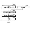
- FIG. 12 is a flowchart relating to the adjustment method of the exposure apparatus of the first embodiment.
- FIG. 13 is a perspective view showing the arrangement of the main parts of the exposure apparatus of the second embodiment.
- FIG. 14 is a perspective view showing the arrangement of the main parts of the exposure apparatus of the third embodiment.
- FIG. 15 is a view showing the arrangement of the rotating drum and the drawing apparatus of the exposure apparatus of the fourth embodiment.
- FIG. 16 is a plan view showing the arrangement of encoder heads of the exposure apparatus of the fifth embodiment.
- FIG. 17 is a plan view showing the arrangement of scale disks of the exposure apparatus of the sixth embodiment.
- FIG. 18 is a flowchart showing device manufacturing methods according to the first to fifth embodiments.
- FIG. 1 is a view showing the overall configuration of an exposure apparatus (substrate processing apparatus) according to the first embodiment.
- the substrate processing apparatus of the first embodiment is an exposure apparatus EX that performs an exposure process on a substrate P, and the exposure apparatus EX is incorporated in a device manufacturing system 1 that performs various processes on the exposed substrate P to manufacture devices. ing. First, the device manufacturing system 1 will be described.
- the device manufacturing system 1 is a line for manufacturing a flexible display as a device (flexible display manufacturing line).
- Examples of the flexible display include an organic EL display.
- the substrate P is sent out from a supply roll (not shown) in which a flexible substrate P is wound in a roll shape, and various processes are continuously performed on the sent out substrate P. Then, a so-called roll-to-roll system is adopted in which the processed substrate P is wound as a flexible device on a collection roll (not shown).
- a substrate P that is a film-like sheet is sent out from a supply roll, and the substrate P sent out from the supply roll is sequentially processed into a process apparatus U1, an exposure apparatus EX, and a process apparatus.
- a process apparatus U1 an exposure apparatus EX, and a process apparatus.
- U2 The example until it winds up by the collection
- substrate P used as the process target of the device manufacturing system 1 is demonstrated.
- a foil (foil) made of a resin or a metal such as stainless steel or an alloy is used.
- the resin film material include polyethylene resin, polypropylene resin, polyester resin, ethylene vinyl copolymer resin, polyvinyl chloride resin, cellulose resin, polyamide resin, polyimide resin, polycarbonate resin, polystyrene resin, and vinyl acetate resin. Includes one or more.
- the thermal expansion coefficient may be set smaller than a threshold corresponding to the process temperature or the like, for example, by mixing an inorganic filler with a resin film.
- the inorganic filler may be, for example, titanium oxide, zinc oxide, alumina, silicon oxide or the like.
- the substrate P may be a single layer of ultrathin glass having a thickness of about 100 ⁇ m manufactured by a float process or the like, or a laminate in which the above resin film, foil, or the like is bonded to the ultrathin glass. It may be.
- the substrate P thus configured becomes a supply roll by being wound in a roll shape, and this supply roll is mounted on the device manufacturing system 1.
- the device manufacturing system 1 equipped with the supply roll repeatedly executes various processes for manufacturing the device on the substrate P sent out from the supply roll. For this reason, the processed substrate P is in a state where a plurality of devices are connected. That is, the substrate P sent out from the supply roll is a multi-sided substrate.
- the substrate P may be activated by modifying the surface in advance by a predetermined pretreatment, or may be formed with a fine partition structure (uneven structure) for precise patterning on the surface.
- the treated substrate P is recovered as a recovery roll by being wound into a roll.
- the collection roll is attached to a dicing device (not shown).
- the dicing apparatus equipped with the collection roll divides the processed substrate P for each device (dicing) to form a plurality of devices.
- the dimension in the width direction (short direction) is about 10 cm to 2 m
- the dimension in the length direction (long direction) is 10 m or more.
- substrate P is not limited to an above-described dimension.
- the device manufacturing system 1 includes a process apparatus U1, an exposure apparatus EX, and a process apparatus U2.
- FIG. 1 an orthogonal coordinate system in which the X direction, the Y direction, and the Z direction are orthogonal to each other is shown.
- the X direction is a direction from the process apparatus U1 to the process apparatus U2 through the exposure apparatus EX in the horizontal plane.
- the Y direction is a direction orthogonal to the X direction in the horizontal plane, and is the width direction of the substrate P.
- the Z direction is a direction (vertical direction) orthogonal to the X direction and the Y direction.
- the process apparatus U1 performs a pre-process (pre-process) on the substrate P subjected to the exposure process by the exposure apparatus EX.
- the process apparatus U1 sends the preprocessed substrate P toward the exposure apparatus EX.
- the substrate P sent to the exposure apparatus EX is a substrate (photosensitive substrate) P having a photosensitive functional layer (photosensitive layer) formed on the surface thereof.
- the photosensitive functional layer is applied as a solution on the substrate P and dried to form a layer (film).
- a typical photosensitive functional layer is a photoresist, but as a material that does not require development processing, a photosensitive silane coupling material (SAM) in which the lyophobic property of a portion irradiated with ultraviolet rays is modified, Alternatively, there is a photosensitive reducing material in which a plating reducing group is exposed in a portion that has been irradiated with ultraviolet rays.
- the pattern portion exposed to ultraviolet rays on the substrate P is modified from lyophobic to lyophilic, so that the lyophilic portion A conductive ink (ink containing conductive nanoparticles such as silver and copper) is selectively applied thereon to form a pattern layer.
- a photosensitive reducing material is used as the photosensitive functional layer, since the plating reducing group is exposed to the pattern portion exposed to ultraviolet rays on the substrate P, the substrate P is immediately exposed to a plating solution containing palladium ions after exposure. A pattern layer made of palladium is formed (deposited) by immersing in the substrate for a predetermined time.
- the exposure apparatus EX draws a pattern such as a display circuit or wiring on the substrate P supplied from the process apparatus U1. Although details will be described later, the exposure apparatus EX exposes the substrate P by a plurality of drawing lines LL1 to LL5 obtained by scanning each of the plurality of drawing beams LB in a predetermined scanning direction.
- the process apparatus U2 performs a post-process (post-process) on the substrate P subjected to the exposure process by the exposure apparatus EX.
- the process apparatus U2 receives the substrate P that has been subjected to the exposure processing by the exposure apparatus EX.
- the process apparatus U2 forms a pattern layer of the device on the substrate P by performing a predetermined process on the substrate P on which the exposure process has been performed.
- FIG. 2 is a perspective view showing the arrangement of the main parts of the exposure apparatus of FIG.
- FIG. 3 is a diagram illustrating an arrangement relationship between the alignment microscope and the drawing lines on the substrate.
- FIG. 4 is a view showing the arrangement of the rotating drum and drawing apparatus of the exposure apparatus of FIG.
- FIG. 5 is a plan view showing the arrangement of the main parts of the exposure apparatus of FIG.
- FIG. 6 is a perspective view showing the configuration of the branching optical system of the exposure apparatus shown in FIG.
- FIG. 7 is a view showing the arrangement relationship of a plurality of scanners in the exposure apparatus of FIG.
- FIG. 8 is a perspective view showing an arrangement relationship among the alignment microscope, the drawing line, and the encoder head on the substrate.
- FIG. 9 is a perspective view showing the surface structure of the rotating drum of the exposure apparatus of FIG.
- the exposure apparatus EX is an exposure apparatus that does not use a mask, that is, a so-called raster scan type drawing exposure apparatus, and scans the drawing beam LB in a predetermined scanning direction while carrying the substrate P in the carrying direction.
- drawing is performed on the surface of the substrate P, and a predetermined pattern is formed on the substrate P.
- the exposure apparatus EX includes a drawing device 11, a substrate transport mechanism 12, alignment microscopes AM1 and AM2, and a control device 16.
- the drawing apparatus 11 has a plurality of drawing modules UW1 to UW5, and draws a predetermined pattern on a part of the substrate P transported by the substrate transport mechanism 12 by the plurality of drawing modules UW1 to UW5.
- the substrate transport mechanism 12 transports the substrate P transported from the process device U1 in the previous process to the process device U2 in the subsequent process at a predetermined speed.
- the alignment microscopes AM1 and AM2 detect an alignment mark or the like previously formed on the substrate P in order to relatively align (align) the pattern drawn on the substrate P with the substrate P.
- the control device 16 controls each part of the exposure apparatus EX and causes each part to execute processing.
- the control device 16 may be a part or all of a host control device that controls the device manufacturing system 1.
- the control device 16 may be a device that is controlled by a higher-level control device and is different from the higher-level control device.
- the control device 16 includes, for example, a computer.
- the exposure apparatus EX includes an apparatus frame 13 (see FIG. 2) that supports the drawing apparatus 11 and the substrate transport mechanism 12, and a rotational position detection mechanism (see FIGS. 4 and 8) 14. Furthermore, a light source device CNT that emits laser light (pulse light) as a drawing beam LB is provided in the exposure apparatus EX. In this exposure apparatus EX, the drawing beam LB emitted from the light source device CNT is guided by the drawing apparatus 11 and projected onto the substrate P transported by the substrate transport mechanism 12.
- the exposure apparatus EX is stored in a temperature control chamber EVC.
- the temperature control chamber EVC is installed on the installation surface E of the manufacturing factory via passive or active vibration isolation units SU1, SU2.
- the anti-vibration units SU1, SU2 are provided on the installation surface E, and reduce vibration from the installation surface E.
- the temperature control chamber EVC suppresses a shape change due to the temperature of the substrate P transported inside by keeping the inside at a predetermined temperature.
- the substrate transport mechanism 12 includes an edge position controller EPC, a driving roller DR4, a tension adjusting roller RT1, a rotating drum (cylindrical drum) DR, a tension adjusting roller RT2, a driving roller DR6, and a drive in order from the upstream side in the transport direction of the substrate P. It has a roller DR7.
- the edge position controller EPC adjusts the position in the width direction of the substrate P transported from the process apparatus U1.
- the edge position controller EPC is arranged so that the position at the end (edge) in the width direction of the substrate P sent from the process apparatus U1 falls within a range of about ⁇ 10 ⁇ m to several tens ⁇ m with respect to the target position. Is moved in the width direction to correct the position of the substrate P in the width direction.
- the driving roller DR4 rotates while pinching both front and back surfaces of the substrate P conveyed from the edge position controller EPC, and conveys the substrate P toward the rotating drum DR by sending the substrate P downstream in the conveyance direction.
- the rotating drum DR rotates around the rotation center line AX2 around the rotation center line AX2 extending in the Y direction while supporting the portion of the substrate P that is subjected to pattern exposure in a cylindrical shape, thereby rotating the substrate P around the rotation center line AX2.
- Transport In order to rotate such a rotating drum DR around the rotation center line AX2, shaft portions Sf2 coaxial with the rotation center line AX2 are provided on both sides of the rotation drum DR.
- Rotational torque from a drive source (not shown) (motor, reduction gear mechanism, etc.) is given to the shaft portion Sf2.
- a surface passing through the rotation center line AX2 and extending in the Z direction is a center surface p3.
- the two sets of tension adjusting rollers RT1 and RT2 give a predetermined tension to the substrate P which is wound around and supported by the rotary drum DR.
- the two sets of drive rollers DR6 and DR7 are arranged at a predetermined interval in the transport direction of the substrate P, and give a predetermined slack (play) DL to the exposed substrate P.
- the drive roller DR6 rotates while sandwiching the upstream side of the substrate P to be transported, and the drive roller DR7 rotates while sandwiching the downstream side of the substrate P to be transported to direct the substrate P toward the process apparatus U2. Transport.
- the slack DL is given to the substrate P, it is possible to absorb fluctuations in the conveyance speed of the substrate P that occur downstream of the driving roller R6 in the conveyance direction, and exposure processing on the substrate P due to fluctuations in the conveyance speed. The influence of can be cut off.
- the substrate transport mechanism 12 adjusts the position of the substrate P transported from the process apparatus U1 in the width direction by the edge position roller EPC.
- the substrate transport mechanism 12 transports the substrate P, whose position in the width direction has been adjusted, to the tension adjustment roller RT1 by the driving roller DR4, and transports the substrate P that has passed through the tension adjustment roller RT1 to the rotary drum DR.
- the substrate transport mechanism 12 transports the substrate P supported by the rotary drum DR toward the tension adjustment roller RT2 by rotating the rotary drum DR.
- the substrate transport mechanism 12 transports the substrate P transported to the tension adjustment roller RT2 to the drive roller DR6, and transports the substrate P transported to the drive roller DR6 to the drive roller DR7. Then, the substrate transport mechanism 12 transports the substrate P toward the process apparatus U2 while giving a slack DL to the substrate P by the driving roller DR6 and the driving roller DR7.
- the exposure apparatus EX includes an apparatus frame 13 that supports the drawing apparatus 11 shown in FIG. 1 and the rotating drum DR of the substrate transport mechanism 12.
- the apparatus frame 13 shown in FIG. 2 includes a main body frame 21, a three-point seat (support mechanism) 22, a first optical surface plate 23, a rotation mechanism 24, and a second optical surface plate in order from the lower side in the Z direction. 25.
- the main body frame 21 is installed on the installation surface E via the vibration isolation units SU1, SU2.
- the main body frame 21 rotatably supports a rotating drum DR and tension adjusting rollers RT1 (not shown) and RT2.
- the first optical surface plate 23 is provided on the upper side in the vertical direction of the rotary drum DR, and is installed on the main body frame 21 via a three-point seat 22.
- the three-point seat 22 supports the first optical surface plate 23 at three support points 22a, and the length of each support point 22a in the Z direction can be adjusted. For this reason, the three-point seat 22 can adjust the inclination of the surface of the first optical surface plate 23 with respect to the horizontal plane to a predetermined inclination.
- the positions in the X and Y directions can be adjusted in the XY plane between the main body frame 21 and the three point seats 22.
- the main body frame 21 and the three-point seat 22 are in a fixed state (rigid state).
- the main body frame 21 and the first optical surface plate 23 connected via the three-point seat 22 function as a first support member.
- the second optical surface plate 25 is provided above the first optical surface plate 23 in the vertical direction, and is installed on the first optical surface plate 23 via the rotation mechanism 24.
- the surface of the second optical surface plate 25 is substantially parallel to the surface of the first optical surface plate 23.
- the rotation mechanism 24 maintains the respective plate surfaces of the first optical surface plate 23 and the second optical surface plate 25 substantially in parallel, and the first optical surface plate 23 is centered on a predetermined rotation axis I extending in the vertical direction. In contrast, the second optical surface plate 25 is rotated.
- the rotation axis I extends in the vertical direction in the center plane p3 and passes through a predetermined point in the surface of the substrate P wound around the rotary drum DR (a drawing surface curved along the circumferential surface). (See FIG. 3). Then, the rotating mechanism 24 rotates the second optical surface plate 25 with respect to the first optical surface plate 23, thereby adjusting the positions of the plurality of drawing modules UW1 to UW5 with respect to the substrate P wound around the rotating drum DR. be able to.
- the light source device CNT is installed on the main body frame 21 of the device frame 13.
- the light source device CNT emits a laser beam as a drawing beam LB projected onto the substrate P.
- the light source device CNT includes a light source that emits light in a predetermined wavelength range suitable for exposure of the photosensitive functional layer on the substrate P and having a strong photoactive action in the ultraviolet range.
- a laser light source emitting YAG third harmonic laser light (wavelength 355 nm) or a wavelength conversion element (harmonic wave) after amplifying seed light in the infrared wavelength region from a semiconductor laser light source with a fiber amplifier.
- a fiber amplifier laser light source that emits laser light in an ultraviolet wavelength region having a wavelength of 400 nm or less can be used.
- the emitted ultraviolet laser light may be continuously oscillated, or may be pulsed laser light that oscillates at a frequency of 100 MHz or more with an emission time per pulse of several tens of picoseconds or less.
- the light source include a lamp light source such as a mercury lamp having a bright line (g-line, h-line, i-line, etc.) in the ultraviolet region, a laser diode having an oscillation peak in the ultraviolet region with a wavelength of 450 nm or less, and a light emitting diode (LED).
- a gas laser light source that generates KrF excimer laser light (wavelength 248 nm), ArF excimer laser light (wavelength 193 nm), XeCl excimer laser light (wavelength 308 nm), etc. that oscillates far ultraviolet light (DUV light) Is available.
- the drawing beam LB emitted from the light source device CNT enters a polarization beam splitter PBS described later.
- the drawing beam LB is preferably a light beam such that almost all of the incident drawing beam LB is reflected by the polarization beam splitter PBS in order to suppress energy loss due to separation of the drawing beam LB by the polarization beam splitter PBS.
- the polarization beam splitter PBS reflects a light beam that becomes S-polarized linearly polarized light and transmits a light beam that becomes P-polarized linearly polarized light.
- the light source device CNT it is preferable to emit a laser beam in which the drawing beam LB incident on the polarization beam splitter PBS is a linearly polarized light (S-polarized light). Moreover, since the laser beam has a high energy density, it is possible to appropriately ensure the illuminance of the light beam projected onto the substrate P.
- the drawing apparatus 11 is a so-called multi-beam type drawing apparatus 11 using a plurality of drawing modules UW1 to UW5.
- the drawing device 11 branches the drawing beam LB emitted from the light source device CNT into a plurality of drawing beams, and a plurality of drawing beams LB (for example, five in the first embodiment) on the substrate P are drawn. Scanning is performed along LL1 to LL5. Then, the drawing apparatus 11 stitches the patterns drawn on the substrate P by each of the plurality of drawing lines LL1 to LL5 in the width direction of the substrate P.
- a plurality of drawing lines LL1 to LL5 formed on the substrate P by scanning a plurality of drawing beams LB by the drawing apparatus 11 will be described with reference to FIG.
- the plurality of drawing lines LL1 to LL5 are arranged in two rows in the circumferential direction of the rotary drum DR with the center plane p3 interposed therebetween.
- odd-numbered first drawing lines LL1, third drawing lines LL3, and fifth drawing lines LL5 are arranged on the upstream substrate P in the rotation direction.
- even-numbered second drawing lines LL2 and fourth drawing lines LL4 are arranged on the substrate P on the downstream side in the rotation direction.
- Each drawing line LL1 to LL5 is formed along the width direction (Y direction) of the substrate P, that is, along the rotation center line AX2 of the rotating drum DR, and is shorter than the length of the substrate P in the width direction. More precisely, each of the drawing lines LL1 to LL5 is such that when the substrate P is transported at the reference speed by the substrate transport mechanism 12, the pattern splicing error obtained by the plurality of drawing lines LL1 to LL5 is minimized. It is slightly inclined by a predetermined angle with respect to the rotation center line AX2 of the rotary drum DR.
- the odd-numbered first drawing line LL1, third drawing line LL3, and fifth drawing line LL5 are arranged at a predetermined interval in the direction (axial direction) in which the rotation center line AX2 of the rotary drum DR extends. Further, the even-numbered second drawing line LL2 and fourth drawing line LL4 are arranged at a predetermined interval in the axial direction of the rotary drum DR. At this time, the second drawing line LL2 is arranged between the first drawing line LL1 and the third drawing line LL3 in the axial direction. Similarly, the third drawing line LL3 is disposed between the second drawing line LL2 and the fourth drawing line LL4 in the axial direction.
- the fourth drawing line LL4 is arranged between the third drawing line LL3 and the fifth drawing line LL5 in the axial direction.
- the first to fifth drawing lines LL1 to LL5 are arranged so as to cover the entire width in the width direction (axial direction) of the exposure region A7 drawn on the substrate P.
- the scanning direction of the drawing beam LB scanned along the odd-numbered first drawing line LL1, third drawing line LL3, and fifth drawing line LL5 is a one-dimensional direction and is the same direction.
- the scanning direction of the drawing beam LB scanned along the even-numbered second drawing line LL2 and fourth drawing line LL4 is a one-dimensional direction and is the same direction.
- the scanning direction of the drawing beam LB scanned along the odd-numbered drawing lines LL1, LL3, LL5 and the scanning direction of the drawing beam LB scanned along the even-numbered drawing lines LL2, LL4 are: The reverse direction.
- the drawing start positions of the odd-numbered drawing lines LL1, LL3, LL5 and the drawing start positions of the even-numbered drawing lines LL2, LL4 are adjacent to each other.
- the drawing end positions of the drawing lines LL1, LL3, and LL5 are adjacent to the drawing end positions of the even-numbered drawing lines LL2 and LL4.
- the drawing apparatus 11 performs calibration with the plurality of drawing modules UW1 to UW5 described above, the beam distribution optical system SL that branches the drawing beam LB from the light source device CNT and guides it to the plurality of drawing modules UW1 to UW5. And a calibration detection system 31.
- the beam distribution optical system SL branches the drawing beam LB emitted from the light source device CNT into a plurality of parts and guides the plurality of branched drawing beams LB toward the plurality of drawing modules UW1 to UW5, respectively.
- the beam distribution optical system SL has a first optical system 41 that divides the drawing beam LB emitted from the light source device CNT into two and a second drawing beam LB that is branched by the first optical system 41. It has an optical system 42 and a third optical system 43 to which the other drawing beam LB branched by the first optical system 41 is irradiated.
- the beam distribution optical system SL includes an XY herbing adjustment mechanism 44 and an XY herbing adjustment mechanism 45. In the beam distribution optical system SL, a part on the light source device CNT side is installed on the main body frame 21, while the other part on the drawing modules UW1 to UW5 side is installed on the second optical surface plate 25.
- the first optical system 41 includes a half-wave plate 51, a polarizing mirror 52, a beam diffuser 53, a first reflecting mirror 54, a first relay lens 55, a second relay lens 56, and a second reflecting mirror. 57, a third reflection mirror 58, a fourth reflection mirror 59, and a first beam splitter 60.
- the drawing beam LB emitted from the light source device CNT in the + X direction is applied to the half-wave plate 51.
- the half-wave plate 51 is rotatable in the irradiation surface of the drawing beam LB.
- the polarization direction of the drawing beam LB irradiated on the half-wave plate 51 is a predetermined polarization direction corresponding to the rotation amount of the half-wave plate 51.
- the drawing beam LB that has passed through the half-wave plate 51 is applied to a polarizing mirror (deflection beam splitter) 52.
- the polarizing mirror 52 transmits the drawing beam LB having a predetermined polarization direction, and reflects the drawing beam LB other than the predetermined polarization direction in the + Y direction.
- the half-wave plate 51 is cooperated by the half-wave plate 51 and the polarizing mirror 52.
- the beam intensity corresponds to the amount of rotation. That is, the beam intensity of the drawing beam LB reflected by the polarizing mirror 52 can be adjusted by rotating the half-wave plate 51 and changing the polarization direction of the drawing beam LB.
- the drawing beam LB transmitted through the polarizing mirror 52 is irradiated to the beam diffuser 53.
- the beam diffuser 53 absorbs the drawing beam LB and suppresses leakage of the drawing beam LB irradiated to the beam diffuser 53 to the outside.
- the drawing beam LB reflected by the polarizing mirror 52 in the + Y direction is applied to the first reflecting mirror 54.
- the drawing beam LB irradiated on the first reflecting mirror 54 is reflected in the + X direction by the first reflecting mirror 54, and is irradiated on the second reflecting mirror 57 via the first relay lens 55 and the second relay lens 56. .
- the drawing beam LB irradiated on the second reflecting mirror 57 is reflected in the ⁇ Y direction by the second reflecting mirror 57 and is irradiated on the third reflecting mirror 58.
- the drawing beam LB irradiated on the third reflecting mirror 58 is reflected in the ⁇ Z direction by the third reflecting mirror 58 and then irradiated on the fourth reflecting mirror 59.
- the drawing beam LB irradiated on the fourth reflecting mirror 59 is reflected in the + Y direction by the fourth reflecting mirror 59 and irradiated on the first beam splitter 60.
- a part of the drawing beam LB irradiated to the first beam splitter 60 is reflected in the ⁇ X direction and irradiated to the second optical system 42, while the other part is transmitted and transmitted to the third optical system 43. Is irradiated.
- the third reflection mirror 58 and the fourth reflection mirror 59 are provided on the rotation axis I of the rotation mechanism 24 at a predetermined interval.
- the configuration up to the light source device CNT including the third reflection mirror 58 (the portion surrounded by the two-dot chain line on the upper side in the Z direction in FIG. 4) is installed on the main body frame 21 side, while the fourth reflection mirror.
- a configuration including a plurality of drawing modules UW1 to UW5 including 59 (a portion surrounded by a two-dot chain line on the lower side in the Z direction in FIG. 4) is installed on the second optical surface plate 25 side.
- the drawing beam LB emitted from the light source device CNT installed on the main body frame 21 side is used as the second optical surface plate. It is possible to suitably guide the drawing modules UW1 to UW5 installed on the surface plate 25 side.
- the second optical system 42 branches and guides one drawing beam LB branched by the first optical system 41 toward odd-numbered drawing modules UW1, UW3, UW5 described later.
- the second optical system 42 includes a fifth reflection mirror 61, a second beam splitter 62, a third beam splitter 63, and a sixth reflection mirror 64.
- the drawing beam LB reflected in the ⁇ X direction by the first beam splitter 60 of the first optical system 41 is applied to the fifth reflecting mirror 61.
- the drawing beam LB irradiated on the fifth reflecting mirror 61 is reflected in the ⁇ Y direction by the fifth reflecting mirror 61 and is irradiated on the second beam splitter 62.
- a part of the drawing beam LB irradiated to the second beam splitter 62 is reflected and irradiated to an odd-numbered drawing module UW5 (see FIG. 5).
- the other part of the drawing beam LB irradiated on the second beam splitter 62 is transmitted and irradiated on the third beam splitter 63.
- the drawing beam LB irradiated to the third beam splitter 63 is reflected and irradiated to one odd-numbered drawing module UW3 (see FIG. 5).
- the other part of the drawing beam LB irradiated to the third beam splitter 63 is transmitted and irradiated to the sixth reflecting mirror 64.
- the drawing beam LB irradiated to the sixth reflecting mirror 64 is reflected by the sixth reflecting mirror 64 and irradiated to an odd-numbered drawing module UW1 (see FIG. 5).
- the drawing beam LB irradiated to the odd-numbered drawing modules UW1, UW3, UW5 is slightly inclined with respect to the ⁇ Z direction (Z axis).
- the third optical system 43 branches the other drawing beam LB branched by the first optical system 41 toward even-numbered drawing modules UW2 and UW4 described later.
- the third optical system 43 includes a seventh reflection mirror 71, an eighth reflection mirror 72, a fourth beam splitter 73, and a ninth reflection mirror 74.
- the drawing beam LB transmitted in the Y direction by the first beam splitter 60 of the first optical system 41 is applied to the seventh reflection mirror 71.
- the drawing beam LB irradiated to the seventh reflection mirror 71 is reflected in the X direction by the seventh reflection mirror 71 and irradiated to the eighth reflection mirror 72.
- the drawing beam LB irradiated on the eighth reflecting mirror 72 is reflected in the ⁇ Y direction by the eighth reflecting mirror 72 and irradiated on the fourth beam splitter 73.
- a part of the drawing beam LB irradiated to the fourth beam splitter 73 is reflected and irradiated to one even-numbered drawing module UW4 (see FIG. 5).
- the other part of the drawing beam LB irradiated to the fourth beam splitter 73 is transmitted and irradiated to the ninth reflecting mirror 74.
- the drawing beam LB irradiated to the ninth reflecting mirror 74 is reflected by the ninth reflecting mirror 74 and irradiated to one even-numbered drawing module UW2.
- the drawing beam LB irradiated to the even-numbered drawing modules UW2 and UW4 is slightly inclined with respect to the ⁇ Z direction (Z axis).
- the drawing beam LB from the light source device CNT is branched into a plurality of parts toward the plurality of drawing modules UW1 to UW5.
- the first beam splitter 60, the second beam splitter 62, the third beam splitter 63, and the fourth beam splitter 73 have the same beam intensity of the drawing beam LB irradiated to the plurality of drawing modules UW1 to UW5.
- the reflectance is set to an appropriate reflectance according to the number of branches of the drawing beam LB.
- the XY herving adjustment mechanism 44 is disposed between the second relay lens 56 and the second reflection mirror 57.
- the XY herbing adjustment mechanism 44 adjusts all the drawing lines LL1 to LL5 formed on the substrate P so that they can be slightly moved within the drawing surface of the substrate P.
- the XY herbing adjustment mechanism 44 includes a transparent parallel flat glass that can be tilted in the XZ plane of FIG. 6 and a transparent parallel flat glass that can be tilted in the YZ plane of FIG.
- the drawing lines LL1 to LL5 formed on the substrate P can be slightly shifted in the X direction or the Y direction by adjusting the inclination amounts of the two parallel flat glass plates.
- the XY herving adjustment mechanism 45 is disposed between the seventh reflection mirror 71 and the eighth reflection mirror 72.
- the XY herving adjustment mechanism 45 adjusts the even-numbered second drawing line LL2 and fourth drawing line LL4 among the drawing lines LL1 to LL5 formed on the substrate P so as to be slightly movable within the drawing surface of the substrate P.
- the XY herbing adjustment mechanism 45 includes a transparent parallel flat glass that can be tilted in the XZ plane of FIG. 6 and a transparent parallel flat glass that can be tilted in the YZ plane of FIG. Composed.
- the drawing lines LL2 and LL4 formed on the substrate P can be slightly shifted in the X direction and the Y direction by adjusting the inclination amounts of the two parallel flat glass plates.
- the plurality of drawing modules UW1 to UW5 are provided according to the plurality of drawing lines LL1 to LL5.
- the plurality of drawing modules UW1 to UW5 are respectively irradiated with a plurality of drawing beams LB branched by the beam distribution optical system SL.
- Each of the drawing modules UW1 to UW5 guides a plurality of drawing beams LB to the drawing lines LL1 to LL5, respectively.
- the first drawing module UW1 guides the drawing beam LB to the first drawing line LL1, and similarly, the second to fifth drawing modules UW2 to UW5 send the drawing beam LB to the second to fifth drawing lines LL2 to LL5.
- the plurality of drawing modules UW1 to UW5 are arranged in two rows in the circumferential direction of the rotary drum DR with the center surface p3 interposed therebetween.
- the plurality of drawing modules UW1 to UW5 have the first drawing on the side where the first, third, and fifth drawing lines LL1, LL3, and LL5 are arranged (the ⁇ X direction side in FIG. 5) across the center plane p3.
- a module UW1, a third drawing module UW3, and a fifth drawing module UW5 are arranged.
- the first drawing module UW1, the third drawing module UW3, and the fifth drawing module UW5 are arranged at a predetermined interval in the Y direction.
- the plurality of drawing modules UW1 to UW5 have the second drawing module UW2 and the second drawing module UW2 on the side where the second and fourth drawing lines LL2 and LL4 are arranged (the + X direction side in FIG. 5) across the center plane p3.
- Four drawing modules UW4 are arranged.
- the second drawing module UW2 and the fourth drawing module UW4 are arranged at a predetermined interval in the Y direction.
- the second drawing module UW2 is located between the first drawing module UW1 and the third drawing module UW3 in the Y direction.
- the third drawing module UW3 is located between the second drawing module UW2 and the fourth drawing module UW4 in the Y direction.
- the fourth drawing module UW4 is located between the third drawing module UW3 and the fifth drawing module UW5 in the Y direction.
- the first drawing module UW1, the third drawing module UW3, and the fifth drawing module UW5, and the second drawing module UW2 and the fourth drawing module UW4 have a center plane p3 as viewed from the Y direction. It is arranged symmetrically in the center.
- drawing modules UW1 to UW5 will be described with reference to FIG. Since the drawing modules UW1 to UW5 have the same configuration, the first drawing module UW1 (hereinafter simply referred to as the drawing module UW1) will be described as an example.
- the drawing module UW1 illustrated in FIG. 4 includes an optical deflector 81, a polarization beam splitter PBS, a quarter-wave plate 82, and a scanning beam LB along the drawing line LL1 (first drawing line LL1).
- a scanner 83, a bending mirror 84, a telecentric f- ⁇ lens system 85, and a Y magnification correcting optical member 86 are provided.
- a calibration detection system 31 is provided adjacent to the deflection beam splitter PBS.
- the optical deflector 81 uses, for example, an acousto-optic modulation element (AOM).
- AOM acousto-optic modulation element
- the optical deflector 81 is switched ON / OFF by the control device 16 to switch projection / non-projection of the drawing beam LB onto the substrate P at high speed.
- the drawing beam LB from the beam distribution optical system SL is irradiated onto the optical deflector 81 through the relay lens 91 in the second optical system 42 with a slight inclination with respect to the ⁇ Z direction.
- the optical deflector 81 is switched OFF, the light beam LB travels straight in an inclined state and is shielded from light by a light shielding plate 92 provided at the end after passing through the optical deflector 81.
- the drawing beam LB incident on the optical deflector 81 becomes a first-order diffracted beam, is deflected in the ⁇ Z direction, and is emitted from the optical deflector 81. Irradiation is performed on a deflecting beam splitter PBS provided in the Z direction of the optical deflector 81. For this reason, the optical deflector 81 projects the drawing beam LB onto the substrate P when switched on and makes the drawing beam LB non-projected onto the substrate P when switched off.
- the deflection beam splitter PBS reflects the drawing beam LB irradiated from the optical deflector 81 via the relay lens 93.
- the deflecting beam splitter PBS cooperates with the quarter wavelength plate 82 provided between the deflecting beam splitter PBS and the scanner 83 to irradiate the drawing beam LB (spot light) and rotate the substrate P (or rotate).
- the reflected light generated on the outer peripheral surface of the drum DR is transmitted. That is, the drawing beam LB irradiated from the optical deflector 81 to the polarization beam splitter PBS is a laser beam that becomes S-polarized linearly polarized light and is reflected by the polarization beam splitter PBS.
- the drawing beam LB reflected by the polarization beam splitter PBS passes through the quarter-wave plate 82 and is irradiated onto the substrate P, and again passes through the quarter-wave plate 82 from the substrate P, so that the P-polarized light is transmitted.
- the laser beam becomes linearly polarized light.
- the reflected light generated from the substrate P (or the outer peripheral surface of the rotating drum DR) and applied to the polarization beam splitter PBS is transmitted through the polarization beam splitter PBS.
- the reflected light that has passed through the polarization beam splitter PBS is applied to the calibration detection system 31 via the relay lens 94.
- the drawing beam LB reflected by the deflecting beam splitter PBS passes through the quarter wavelength plate 82 and is irradiated to the scanner 83.
- the scanner 83 includes a reflection mirror 96, a rotating polygon mirror (rotating polygonal mirror) 97, and an origin detector 98.
- the drawing beam LB that has passed through the quarter-wave plate 82 is applied to the reflection mirror 96 via the relay lens 95.
- the drawing beam LB reflected by the reflecting mirror 96 is directed to the rotating polygon mirror 97.
- the rotating polygon mirror 97 includes a rotating shaft 97a extending in the Z direction and a plurality of reflecting surfaces (for example, eight surfaces) 97b formed around the rotating shaft 97a.
- the rotating polygon mirror 97 continuously changes the reflection angle of the drawing beam LB irradiated to the reflecting surface 97b by rotating it in a predetermined rotation direction around the rotation axis 97a, thereby reflecting the reflected drawing beam LB.
- the drawing beam LB reflected by the rotating polygon mirror 97 is applied to the bending mirror 84.
- the origin detector 98 detects the origin of the drawing beam LB scanned along the drawing line LL1 of the substrate P.
- the origin detector 98 is disposed on the opposite side of the reflecting mirror 96 with the drawing beam LB reflected by each reflecting surface 97b interposed therebetween.
- the origin detector 98 detects the drawing beam LB before being irradiated onto the f- ⁇ lens system 85. That is, the origin detector 98 detects the passage of the drawing beam LB at a timing immediately before the drawing start position of the drawing line LL1 on the substrate P is irradiated.
- the drawing beam LB irradiated to the bending mirror 84 from the scanner 83 is reflected by the bending mirror 84 and irradiated to the f- ⁇ lens system 85.
- the f- ⁇ lens system 85 includes a telecentric f- ⁇ lens, and projects the drawing beam LB reflected from the rotating polygon mirror 97 via the bending mirror 84 perpendicularly to the drawing surface of the substrate P.
- the reflecting surfaces 97b of the rotating polygon mirror 97 and the drawing surface of the substrate P are optically conjugate with respect to the sub-scanning direction (long direction of the substrate P) orthogonal to the drawing line LL1.
- a cylindrical lens (not shown) is arranged in each of the optical path of the drawing beam LB toward the rotating polygon mirror 97 and the optical path of the drawing beam LB emitted from the f- ⁇ lens system 85.
- a collaborative surface tilt correction optical system is also provided.
- the plurality of scanners 83 in the plurality of drawing modules UW1 to UW5 have a symmetrical configuration with the center plane p3 interposed therebetween.
- three scanners 83 corresponding to the drawing modules UW1, UW3, and UW5 are arranged on the upstream side in the rotation direction of the rotary drum DR (the ⁇ X direction side in FIG. 7), and the drawing modules UW2,
- Two scanners 83 corresponding to UW4 are arranged on the downstream side in the rotation direction of the rotary drum DR (the + X direction side in FIG. 7).
- the three upstream scanners 83 and the two downstream scanners 83 are arranged to face each other across the center plane p3.
- each scanner 83 arranged on the upstream side and each scanner 83 arranged on the downstream side are configured to be 180 ° point-symmetric about the rotation axis I. For this reason, when the rotating polygon mirror 97 is irradiated with the drawing beam LB while the three upstream rotating polygon mirrors 97 rotate counterclockwise (counterclockwise in the XY plane), they are reflected by the rotating polygon mirror 97.
- the drawing beam LB is scanned in a predetermined scanning direction (for example, the + Y direction in FIG. 7) from the drawing start position to the drawing end position.
- the drawing beam LB reflected by the rotating polygon mirror 97 is changed to the drawing start position. Is scanned in the scanning direction (for example, the ⁇ Y direction in FIG. 7) opposite to the upstream three rotating polygon mirrors 97 from the drawing end position to the drawing end position.
- the axis of the drawing beam LB reaching the substrate P from the odd-numbered drawing modules UW1, UW3, UW5 is in a direction that coincides with the installation direction line Le1. That is, the installation orientation line Le1 is a line connecting the odd-numbered drawing lines LL1, LL3, LL5 and the rotation center line AX2 in the XZ plane.
- the axis of the drawing beam LB reaching the substrate P from the even-numbered drawing modules UW2 and UW4 is in a direction that coincides with the installation orientation line Le2. That is, the installation orientation line Le2 is a line connecting the even-numbered drawing lines LL2 and LL4 and the rotation center line AX2 in the XZ plane.
- the Y magnification correcting optical member 86 is disposed between the f- ⁇ lens system 85 and the substrate P.
- the Y magnification correcting optical member 86 enlarges or reduces the dimension in the Y direction of the drawing lines LL1 to LL5 formed by the drawing modules UW1 to UW5 by a small amount.
- the drawing device 11 configured as described above draws a predetermined pattern on the substrate P by controlling each part by the control device 16.
- the control device 16 determines the optical deflector based on the CAD information (for example, bitmap format) of the pattern to be drawn on the substrate P during the period in which the drawing beam LB projected on the substrate P is scanned in the scanning direction.
- the drawing beam LB is deflected by ON / OFF modulation of 81, and a pattern is drawn on the photosensitive layer of the substrate P.
- the control device 16 synchronizes the scanning direction of the drawing beam LB that scans along the drawing line LL1 and the movement in the transport direction of the substrate P due to the rotation of the rotary drum DR, so that the drawing line in the exposure region A7.
- a predetermined pattern is drawn on the portion corresponding to LL1.
- the size (spot diameter) of the drawing beam LB projected from each of the drawing modules UW1 to UW5 on the substrate P is D ( ⁇ m)
- the scanning speed of the drawing beam LB along the drawing lines LL1 to LL5 is V ( ⁇ m).
- the light emission repetition period T (second) of the pulsed light has a relationship of T ⁇ D / V.
- the alignment microscopes AM1 and AM2 detect an alignment mark formed in advance on the substrate P, or a reference mark or reference pattern formed on the rotary drum DR.
- the alignment mark of the substrate P and the reference mark or reference pattern of the rotating drum DR are simply referred to as a mark.
- the alignment microscopes AM1 and AM2 are used to align (align) the substrate P and a predetermined pattern drawn on the substrate P, and to calibrate the rotary drum DR and the drawing device 11.
- Alignment microscopes AM1 and AM2 are provided upstream of the drawing lines LL1 to LL5 formed by the drawing apparatus 11 in the rotation direction of the rotary drum DR. Further, the alignment microscope AM1 is arranged on the upstream side in the rotation direction of the rotary drum DR as compared with the alignment microscope AM2.
- the alignment microscopes AM1 and AM2 project the illumination light onto the substrate P or the rotating drum DR, and the objective lens system GA serving as a detection probe that receives the light generated by the mark, and the image of the mark received via the objective lens system GA.
- An imaging system GD or the like that captures (bright-field image, dark-field image, fluorescent image, etc.) with a two-dimensional CCD, CMOS, or the like.
- the illumination light for alignment is light in a wavelength region that has little sensitivity to the photosensitive layer on the substrate P, for example, light having a wavelength of about 500 to 800 nm.
- Alignment microscopes AM1 are provided in a plurality (for example, three) in a line in the Y direction (width direction of the substrate P). Similarly, a plurality of (for example, three) alignment microscopes AM2 are provided in a line in the Y direction (the width direction of the substrate P). That is, a total of six alignment microscopes AM1 and AM2 are provided.
- FIG. 3 shows the arrangement of the objective lens systems GA1 to GA3 of the three alignment microscopes AM1 among the objective lens systems GA of the six alignment microscopes AM1 and AM2 for easy understanding.
- the observation regions Vw1 to Vw3 on the substrate P (or the outer peripheral surface of the rotating drum DR) by the objective lens systems GA1 to GA3 of the three alignment microscopes AM1 are in the Y direction parallel to the rotation center line AX2, as shown in FIG. Are arranged at predetermined intervals.
- the optical axes La1 to La3 of the objective lens systems GA1 to GA3 passing through the centers of the observation regions Vw1 to Vw3 are all parallel to the XZ plane.
- observation regions Vw4 to Vw6 on the substrate P (or the outer peripheral surface of the rotary drum DR) by the objective lens systems GA of the three alignment microscopes AM2 are Y parallel to the rotation center line AX2, as shown in FIG. Arranged at predetermined intervals in the direction.
- the optical axes La4 to La6 of each objective lens system GA passing through the centers of the observation regions Vw4 to Vw6 are all parallel to the XZ plane.
- the observation areas Vw1 to Vw3 and the observation areas Vw4 to Vw6 are arranged at a predetermined interval in the rotation direction of the rotary drum DR.
- the mark observation regions Vw1 to Vw6 by the alignment microscopes AM1 and AM2 are set on the substrate P or the rotating drum DR, for example, in a range of about 200 to 500 ⁇ m square.
- the optical axes La1 to La3 of the alignment microscope AM1 that is, the optical axes La1 to La3 of the objective lens system GA, are set in the same direction as the installation orientation line Le3 extending in the radial direction of the rotary drum DR from the rotation center line AX2.
- the installation direction line Le3 is a line connecting the observation areas Vw1 to Vw3 of the alignment microscope AM1 and the rotation center line AX2 when viewed in the XZ plane of FIG.
- the optical axes La4 to La6 of the alignment microscope AM2 are set in the same direction as the installation direction line Le4 extending in the radial direction of the rotary drum DR from the rotation center line AX2.
- the That is, the installation direction line Le4 is a line connecting the observation areas Vw4 to Vw6 of the alignment microscope AM2 and the rotation center line AX2 when viewed in the XZ plane of FIG.
- the angle formed by the center plane p3 and the installation orientation line Le3 is the same as that of the center plane p3. It is larger than the angle formed by the installation orientation line Le4.
- an exposure area A7 drawn by each of the five drawing lines LL1 to LL5 is arranged at a predetermined interval in the X direction.
- a plurality of alignment marks Ks1 to Ks3 (hereinafter abbreviated as marks) for alignment are formed in a cross shape, for example.
- the mark Ks1 is provided in the peripheral area on the ⁇ Y side of the exposure area A7 at a constant interval in the X direction, and the mark Ks3 is fixed in the peripheral area on the + Y side of the exposure area A7 in the X direction. Provided at intervals. Further, the mark Ks2 is provided at the center in the Y direction in a blank area between two exposure areas A7 adjacent in the X direction.
- the marks Ks1 are sequentially captured while the substrate P is being sent in the observation region Vw1 of the objective lens system GA1 of the alignment microscope AM1 and in the observation region Vw4 of the objective lens system GA of the alignment microscope AM2. Formed. Further, the mark Ks3 is sequentially captured while the substrate P is being sent in the observation region Vw3 of the objective lens system GA3 of the alignment microscope AM1 and in the observation region Vw6 of the objective lens system GA of the alignment microscope AM2. Formed. Further, the marks Ks2 are sequentially captured while the substrate P is being sent in the observation region Vw2 of the objective lens system GA2 of the alignment microscope AM1 and in the observation region Vw5 of the objective lens system GA of the alignment microscope AM2. It is formed so that.
- the alignment microscopes AM1 and AM2 on both sides in the Y direction of the rotating drum DR constantly observe or detect the marks Ks1 and Ks3 formed on both sides in the width direction of the substrate P. be able to.
- the center alignment microscope AM1 and AM2 in the Y direction of the rotary drum DR is a mark formed in a blank portion between the exposure areas A7 drawn on the substrate P. Ks2 can always be observed or detected.
- the exposure apparatus EX uses a so-called multi-beam type drawing apparatus 11
- a plurality of patterns drawn on the substrate P are drawn by the drawing lines LL1 to LL5 of the plurality of drawing modules UW1 to UW5.
- Calibration in order to keep the joining accuracy by the plurality of drawing modules UW1 to UW5 within an allowable range is necessary.
- the relative arrangement relationship of the observation regions Vw1 to Vw6 of the alignment microscopes AM1 and AM2 with respect to the drawing lines LL1 to LL5 of the plurality of drawing modules UW1 to UW5 (or an error amount with respect to the design arrangement interval) is the base line. It is called that the relative arrangement relationship and the amount of error need to be precisely determined by baseline management. Calibration is also required for the baseline management.
- the exposure apparatus EX uses a rotary drum DR provided with a reference mark or a reference pattern on the outer peripheral surface.
- the rotary drum DR has scale portions GPa and GPb that constitute a part of a rotational position detection mechanism 14 described later on both ends of the outer peripheral surface thereof.
- the rotary drum DR is provided with engraved restriction bands CLa and CLb having narrow grooves by concave grooves or convex rims on the inner sides of the scale parts GPa and GPb.
- the width in the Y direction of the substrate P is set to be smaller than the interval in the Y direction between the two regulation bands CLa and CLb, and the substrate P is sandwiched between the regulation bands CLa and CLb on the outer peripheral surface of the rotary drum DR. It is supported in close contact with the inner region.
- the rotating drum DR is inclined on the outer peripheral surface sandwiched between the regulation bands CLa and CLb by a plurality of line patterns RL1 inclined at +45 degrees with respect to the rotation center line AX2, and at ⁇ 45 degrees with respect to the rotation center line AX2.
- a mesh-like reference pattern (which can also be used as a reference mark) RMP in which a plurality of line patterns RL2 are repeatedly engraved at a constant pitch (period) Pf1, Pf2.
- the reference pattern RMP is an oblique pattern (an oblique lattice pattern) that is uniform over the entire surface so that the frictional force, the tension of the substrate P, and the like do not change at the portion where the substrate P and the outer peripheral surface of the rotary drum DR are in contact with each other.
- the line patterns RL1 and RL2 are not necessarily inclined at 45 degrees, and may be a vertical and horizontal mesh pattern in which the line pattern RL1 is parallel to the Y axis and the line pattern RL2 is parallel to the X axis.
- the line patterns RL1 and RL2 do not need to intersect at 90 degrees, and the rectangular region surrounded by the two adjacent line patterns RL1 and the two adjacent line patterns RL2 is other than a square (or a rectangle).
- the line patterns RL1 and RL2 may be crossed at an angle that results in a rhombus.
- the rotational position detection mechanism 14 optically detects the rotational position of the rotary drum DR, and an encoder system using, for example, a rotary encoder is applied.
- the rotational position detection mechanism 14 includes scale parts (indexes) GPa and GPb provided at both ends of the rotary drum DR, and a plurality of encoder heads (read heads) EN1, EN2, EN3 facing the scale parts GPa and GPb. EN4. 4 and 8, only four encoder heads EN1, EN2, EN3, and EN4 that face the scale part GPa are shown, but similar encoder heads EN1, EN2, EN3, and EN4 also face the scale part GPb. (See FIG. 10).
- the scale parts GPa and GPb are respectively formed in an annular shape over the entire circumferential direction of the outer peripheral surface of the rotary drum DR.
- the scales of the scale parts GPa and GPb are diffraction gratings in which concave or convex grating lines are engraved at a constant pitch (for example, 20 ⁇ m) in the circumferential direction of the outer peripheral surface of the rotary drum DR, and are configured as incremental scales. . For this reason, the scale parts GPa and GPb rotate integrally with the rotary drum DR around the rotation center line AX2.
- the substrate P is configured to be wound inside the scale portions GPa and GPb at both ends of the rotary drum DR, that is, inside the regulation bands CLa and CLb.
- the outer peripheral surfaces of the scale portions GPa and GPb and the outer peripheral surface of the portion of the substrate P wound around the rotary drum DR are set to be the same surface (same radius from the center line AX2).
- the outer peripheral surfaces of the scale parts GPa and GPb may be set higher than the outer peripheral surface for winding the substrate of the rotary drum DR by the thickness of the substrate P in the radial direction.
- the outer peripheral surfaces of the scale portions GPa and GPb formed on the rotary drum DR can be set to have substantially the same radius as the outer peripheral surface of the substrate P. Therefore, the encoder heads EN1, EN2, EN3, EN4 can detect the scale portions GPa, GPb at the same radial position as the drawing surface on the substrate P wound around the rotary drum DR, and the measurement position and the processing position can be determined. Abbe errors caused by different radial directions of the rotating system can be reduced.
- Encoder heads EN1, EN2, EN3, and EN4 are respectively disposed around the scale portions GPa and GPb as viewed from the rotation center line AX2, and are located at different positions in the circumferential direction of the rotary drum DR.
- the encoder heads EN1, EN2, EN3, and EN4 are connected to the control device 16.
- the encoder heads EN1, EN2, EN3, and EN4 project measurement light beams toward the scale portions GPa and GPb, and photoelectrically detect the reflected light beams (diffracted light), thereby causing the scale portions GPa and GPb in the circumferential direction.
- a detection signal (for example, a two-phase signal having a phase difference of 90 degrees) corresponding to the position change is output to the control device 16.
- the control device 16 interpolates and digitally processes detection signals (two-phase signals) from each of the encoder heads EN1 to EN4 by a counter circuit (not shown), thereby changing the angle of the rotary drum DR, that is, the encoder head.
- a change in the circumferential position of the outer peripheral surface of the rotary drum DR at each of the installation positions EN1 to EN4 can be measured with submicron resolution.
- the control device 16 can also measure the conveyance speed of the substrate P and the amount of movement in the circumferential direction on the rotating drum DR from the change in angle of the rotating drum DR.
- the encoder head EN1 is disposed on the installation direction line Le1.
- the installation azimuth line Le1 is a line connecting the projection area (detection position) of the measurement light beam on the scale part GPa (GPb) by the encoder head EN1 and the rotation center line AX2 in the XZ plane.
- the installation direction line Le1 is a line connecting the drawing lines LL1, LL3, LL5 and the rotation center line AX2 in the XZ plane. From the above, the line connecting the reading position of the encoder head EN1 and the rotation center line AX2 and the line connecting the drawing lines LL1, LL3, LL5 and the rotation center line AX2 are the same azimuth line.
- the encoder head EN2 is arranged on the installation direction line Le2.
- the installation azimuth line Le2 is a line connecting the projection area of the measurement light beam on the scale part GPa (GPb) by the encoder head EN2 and the rotation center line AX2 in the XZ plane.
- the installation direction line Le2 is a line connecting the drawing lines LL2 and LL4 and the rotation center line AX2 in the XZ plane. From the above, the line connecting the reading position of the encoder head EN2 and the rotation center line AX2 and the line connecting the drawing lines LL2, LL4 and the rotation center line AX2 are the same azimuth line.
- the encoder head EN3 is arranged on the installation direction line Le3.
- the installation azimuth line Le3 is a line connecting the projection area of the measurement light beam on the scale part GPa (GPb) by the encoder head EN3 and the rotation center line AX2 in the XZ plane.
- the installation orientation line Le3 is a line connecting the observation areas Vw1 to Vw3 of the substrate P by the alignment microscope AM1 and the rotation center line AX2 in the XZ plane. From the above, the line connecting the reading position of the encoder head EN3 and the rotation center line AX2 and the line connecting the observation regions Vw1 to Vw3 of the alignment microscope AM1 and the rotation center line AX2 have the same azimuth line.
- the encoder head EN4 is disposed on the installation direction line Le4.
- the installation azimuth line Le4 is a line connecting the projection area of the measurement light beam on the scale part GPa (GPb) by the encoder head EN4 and the rotation center line AX2 in the XZ plane.
- the installation direction line Le4 is a line connecting the observation areas Vw4 to Vw6 of the substrate P by the alignment microscope AM2 and the rotation center line AX2 in the XZ plane. From the above, the line connecting the reading position of the encoder head EN3 and the rotation center line AX2 and the line connecting the observation regions Vw4 to Vw6 of the alignment microscope AM2 and the rotation center line AX2 have the same azimuth line.
- installation directions (angle directions in the XZ plane with the rotation center line AX2 as the center) of the encoder heads EN1, EN2, EN3, EN4 are represented by installation direction lines Le1, Le2, Le3, Le4, as shown in FIG.
- a plurality of drawing modules UW1 to UW5 and encoder heads EN1 and EN2 are arranged so that the installation orientation lines Le1 and Le2 are at an angle ⁇ ⁇ ° with respect to the center plane P3.
- the control device 16 detects the rotation angle positions of the scale units (rotary drums DR) GPa and GPb by the encoder heads EN1 and EN2, and specifies the movement position of the substrate P based on the detected rotation angle positions.
- Drawing control is performed by the odd-numbered and even-numbered drawing modules UW1 to UW5. That is, the control device 16 performs the ON / OFF modulation of the optical deflector 81 based on the CAD information of the pattern to be drawn on the substrate P during the period in which the drawing beam LB projected on the substrate P is scanned in the scanning direction.
- the ON / OFF modulation timing by the optical deflector 81 based on the detected rotation angle position (movement position of the substrate P), a pattern can be accurately drawn on the photosensitive layer of the substrate P. Can do.
- control device 16 rotates the scale portions GPa and GPb (rotary drum DR) detected by the encoder heads EN3 and EN4 when the alignment marks Ks1 to Ks3 on the substrate P are detected by the alignment microscopes AM1 and AM2.
- the control device 16 rotates the scale portions GPa and GPb (rotating drum DR) detected by the encoder heads EN3 and EN4 when the reference pattern RMP on the rotating drum DR is detected by the alignment microscopes AM1 and AM2.
- the alignment microscopes AM1 and AM2 can precisely measure the rotation angle position (or circumferential position) of the rotary drum DR at the moment when the mark is sampled in the observation regions Vw1 to Vw6.
- the exposure apparatus EX based on the measurement result, the substrate P and a predetermined pattern drawn on the substrate P are aligned (aligned), and the rotary drum DR and the drawing apparatus 11 are calibrated. To do.
- the drawing beam LB is scanned along a plurality of drawing lines LL1 to LL5 on the substrate P while the substrate P is being carried in the carrying direction (longitudinal direction) by the rotating drum DR.
- the substrate P is wound and conveyed around a part of the outer peripheral surface of the rotary drum DR, but the positional relationship between the rotary drum DR and the second optical surface plate 25 due to the influence of vibration or the like due to the rotation of the rotary drum DR. May be displaced relatively.
- the displacement of the arrangement relationship between the rotating drum DR and the second optical surface plate 25 is, for example, that the rotation center line AX2 of the rotating drum DR is inclined with respect to the Y direction in the XY plane.
- the relative arrangement relationship between the substrate P wound around the rotary drum DR and the drawing apparatus 11 installed on the second optical surface plate 25 is suitable for exposure by the displacement of the rotary drum DR. It will deviate from a predetermined relative arrangement relationship (initial setting state). Therefore, in the exposure apparatus EX of the first embodiment, the encoder heads EN1 to EN4 are attached as shown in FIG. 10 in order to measure the relative positional relationship between the rotary drum DR and the drawing apparatus 11. .
- FIG. 10 is a plan view showing the arrangement of encoder heads of the exposure apparatus of FIG.
- the encoder heads (first detection devices) EN ⁇ b> 1 and EN ⁇ b> 2 are attached to the second optical surface plate 25 via the attachment member 100.
- the encoder heads (second detection devices) EN3 and EN4 are attached to the main body frame 21 via the attachment member 101, and the alignment microscopes AM1 and AM2 are also attached to the main body frame 21.
- a pair of encoder heads EN1, EN2 is provided corresponding to a pair of scale portions GPa, GPb provided on both sides of the rotation center line AX2 of the rotary drum DR. For this reason, the pair of encoder heads EN1 and EN2 detect the rotational positions of the scale portions GPa and GPb.
- a rotation amount measuring device 105 that measures the rotation amount by the rotation mechanism 24 is provided between the first optical surface plate 23 and the second optical surface plate 25.
- the rotation amount measuring device 105 is, for example, a linear encoder, and is disposed on the far side from the rotation axis I so that the linear movement direction is along the circumferential direction of the rotation axis I.
- the control device 16 detects the amount of rotation of the second optical surface plate 25 relative to the first optical surface plate 23 based on the slight movement amount in the circumferential direction of the rotation axis I detected by the rotation amount measuring device 105.
- the rotation mechanism 24 includes a drive unit 106, and the drive unit 106 is driven and controlled by the control device 16 to rotate the second optical surface plate 25. At this time, the control device 16 controls the drive unit 106 to rotate the second optical surface plate 25 so that the rotation amount detected by the rotation amount measuring device 105 becomes a predetermined rotation amount. Yes.
- FIG. 11 is a plan view for explaining a case where the rotating drum DR and the drawing device 11 (particularly, the second optical surface plate 25) relatively rotate slightly in the XY plane in the configuration of FIG.
- the rotation center line AX2 of the rotary drum DR extends in the Y direction.
- the rotation center line AX2 is the reference.
- the rotation center line AX2 is, the influence of vibration from the drive source in the floor vibration and equipment, and inclined from the reference position by a predetermined angle theta z min.
- a pair of encoder heads EN1, EN2 by rotating center line AX2 tilts from the reference position by a predetermined angle theta z min, the rotational position detected by the encoder head EN1, EN2 scale portion GPa side (scale section a GPa moving position of) the a rotational position detected by the encoder head EN1, EN2 scale portion GPb side (movement position of the scale portion GPb), the difference corresponding to the angle theta z is arise. Therefore, the control unit 16 based on the rotational position detected by the pair of encoder heads EN1, EN2, it is possible to detect the inclination angle theta z of the rotation center line AX2 of the rotary drum DR in the XY plane.
- the count value (the movement position of the scale GPa) counted by the counter circuit corresponding to the encoder head EN1 on the scale portion GPa side is counted by the counter circuit corresponding to the encoder head EN1 on the scale portion GPb side.
- the count value (the movement position of the scale GPb) is CD1b
- the difference value between the count value CD1a and the count value CD1b is changed every time the rotating drum DR (scale parts GPa, GPb) rotates by a certain angle or constant. It is possible to measure the inclination variation (angle ⁇ z ) in the XY plane of the rotation center line AX2 of the rotary drum DR by sequentially obtaining each time and monitoring the change in the difference value.
- the count value (the movement position of the scale GPa) counted by the counter circuit corresponding to the encoder head EN2 on the scale portion GPa side corresponds to the encoder head EN2 on the CD2a and scale portion GPb side.
- the count value counted by the counter circuit (the movement position of the scale GPb) is set as CD2b, and the change in the difference value may be monitored.
- the pair of encoder heads EN1 and the pair of encoder heads EN2 are symmetrically positioned with respect to the X direction with respect to the center plane p3 as shown in FIG. Since it is installed, a change in the difference value between the count value CD1a by the encoder head EN1 facing the scale portion GPa and the count value CD2b by the encoder head EN2 facing the scale portion GPb, or the encoder head EN2 facing the scale portion GPa. It is also possible to monitor the change in the difference value between the count value CD2a due to and the count value CD1b due to the encoder head EN1 facing the scale portion GPb.
- the control device 16 performs the drawing by the drawing device 11 on the substrate P transported by the rotary drum DR, based on the detection results of the alignment microscopes AM1 and AM2, so that the drawing device 11 with respect to the substrate P can perform drawing.
- the position is corrected.
- the control device 16 determines the state of the shape of the substrate P and the deformation of the device pattern (base pattern) region already formed on the substrate P based on the positions of the marks Ks1 to Ks3 detected by the alignment microscopes AM1 and AM2. And a relative correction rotation amount ⁇ 2 corresponding to the detected deformation state (especially inclination) is obtained.
- the corrected rotation amount ⁇ 2 is an angle from a reference line extending in the X direction.
- control apparatus 16 correct
- the control unit 16 based on the relative correction rotation amount theta 2 obtained, the rotation mechanism 24 (second optical flat 25) is rotated corrected from the initial position, the encoder head EN1, EN2 also rotates since it would not be able to consider the inclination theta z rotation center line AX2 to be measured after the rotation correction, i.e. not make sense. Therefore, the control device 16 rotates the rotation mechanism 24 based on the corrected rotation amount ⁇ 2 in consideration of the inclination ⁇ z of the rotation center line AX2 measured in advance (or immediately before).
- the rotation mechanism 24 is rotated while measuring the rotation amount by the rotation mechanism 24 by the rotation amount measuring device 105 so that “)” becomes zero.
- the control device 16 determines the in-plane XY that is the deviation information from the predetermined relative arrangement relationship between the rotary drum DR and the second optical surface plate 25 based on the detection results of the pair of encoder heads EN1 and EN2. Is obtained by calculating the inclination ⁇ z of the rotation center line AX2 (inclination of the rotating drum DR in the XY plane) ⁇ 2, and the correction rotation amount ⁇ 2 corresponding to the inclination in the XY plane of the substrate P obtained by the alignment microscopes AM1 and AM2. and so that the deviation between the inclination theta z of the rotation center line AX2 is reduced, i.e., to maintain a predetermined relative positional relationship, controls the driving unit 106 of the rotation mechanism 24.
- FIG. 12 is a flowchart relating to the adjustment method of the exposure apparatus of the first embodiment.
- the control device 16 first detects the alignment relationship between the rotating drum DR and the second optical surface plate 25 by the alignment microscopes AM1 and AM2 when the rotation mechanism 24 corrects the positional relationship between the rotating drum DR and the second optical surface plate 25 so that the drawing device 11 can draw on the substrate P.
- the detected result (such as the inclination of the device pattern area on the substrate P) is acquired (step S1).
- Control unit 16 based on a detection result detected by the alignment microscope AM1, AM2, obtain the correction amount of rotation theta 2 to be adjusted by the rotation mechanism 24 (step S2).
- control unit 16 from the comparison of the detection result of the pair of encoder heads EN1, EN2, to obtain information relating to inclination theta z (step S3).
- the control device 16 determines the inclination ⁇ z of the rotation center line AX2 based on the respective rotation angle positions (count values CD1a, CD1b, CD2a, CD2b) of the scale portions GPa, GPb detected by the pair of encoder heads EN1, EN2. Is obtained (step S4).
- the control device 16 controls the rotation mechanism 24 by feedback control or the like so that the deviation of the calculated correction rotation amount ⁇ 2 and the inclination ⁇ z of the rotation center line AX2, that is, “ ⁇ 2 ⁇ z ” becomes zero.
- step S5 the control apparatus 16 is again based on each rotation angle position (count value CD1a, CD1b, CD2a, CD2b) of scale part GPa, GPb detected by a pair of encoder head EN1, EN2. Te, finding a new inclination theta 'z the rotation center line AX2 at appropriate time intervals.
- the rotation mechanism 24 is feedback-controlled so that the new inclination ⁇ ′ z is maintained.
- the exposure apparatus EX can rotate the rotating drum in the XY plane based on the detection results of the encoder heads EN1 and EN2. Deviation information (inclination ⁇ z of the rotation center line AX2) from a predetermined relative arrangement relationship between the DR and the second optical surface plate 25 can be obtained. Then, the exposure apparatus EX can correct the relative arrangement relationship between the rotary drum DR and the second optical surface plate 25 based on the obtained deviation information.
- the exposure apparatus EX maintains a predetermined relative arrangement relationship between the rotary drum DR and the second optical surface plate 25 even if the position of the rotary drum DR is displaced due to the influence of vibration or the like due to the rotation of the rotary drum DR. Therefore, it is possible to perform drawing on the substrate P with high accuracy by the drawing apparatus 11.
- the encoder heads EN1 and EN2 can be provided on the installation direction lines Le1 and Le2. Therefore, the direction connecting the encoder head EN1 and the rotation center line AX2 and the direction connecting the odd-numbered drawing lines LL1, LL3, LL5 and the rotation center line AX2 can be made the same direction. Similarly, the direction connecting the encoder head EN2 and the rotation center line AX2 and the direction connecting the even-numbered drawing lines LL2 and LL4 and the rotation center line AX2 can be the same direction. Therefore, the arrangement relationship between the encoder heads EN1 and EN2 and the drawing lines LL1 to LL5 can be matched.
- the encoder heads EN 3 and EN 4 can be attached to the main body frame 21.
- the exposure apparatus EX measures the marks Ks1 to Ks3 by the alignment microscopes AM1 and AM2 based on the detection results of the encoder heads EN3 and EN4, with the main body frame 21 (the bearing portion of the rotating drum DR) as a stationary reference. be able to. Then, the exposure apparatus EX can obtain a relative correction rotation amount ⁇ 2 to be corrected by the rotation mechanism 24 based on the detection results of the alignment microscopes AM1 and AM2.
- the exposure apparatus EX based on the deviation between the inclination theta z of the rotation center line AX2 correction is the rotation amount theta 2 and shift information obtained, precisely the positional relationship between the rotary drum DR and the second optical flat 25 It becomes possible to correct to.
- the encoder heads EN3 and EN4 can be provided on the installation orientation lines Le3 and Le4. For this reason, the direction connecting the encoder head EN3 and the rotation center line AX2 and the direction connecting the observation regions Vw1 to Vw3 and the rotation center line AX2 can be made the same direction. Further, the direction connecting the encoder head EN4 and the rotation center line AX2 and the direction connecting the observation areas Vw4 to Vw6 and the rotation center line AX2 can be the same direction. Therefore, the arrangement relationship between the encoder heads EN3 and EN4 and the arrangement relationship between the observation areas Vw1 to Vw6 can be matched. Therefore, even if the position of the rotating drum DR is displaced, the arrangement relationship of the observation areas Vw1 to Vw6 with respect to the rotating drum DR can be accurately measured by the encoder heads EN3 and EN4. it can.
- the rotational relationship between the rotary drum DR and the second optical surface plate 25 is corrected by rotating the second optical surface plate 25 with respect to the first optical surface plate 23 by the rotation mechanism 24. Can do. Therefore, the exposure apparatus EX corrects the drawing lines LL1 to LL5 formed by the drawing apparatus 11 installed on the second optical surface plate 25 to an appropriate position with respect to the substrate P wound around the rotary drum DR. Thus, the drawing device 11 can perform drawing on the substrate P with high accuracy.
- step S1 and S2 for determining the correction amount of rotation theta 2 after performing the steps S1 and S2 for determining the correction amount of rotation theta 2, but the performance of step S3 and step S4 for obtaining the displacement information is not limited to this configuration.
- the steps S1 and S2 for determining the correction amount of rotation theta 2, to the steps S3 and S4 for obtaining the deviation information may be performed in parallel, perform the steps S3 and S4 for obtaining the deviation information
- step S1 and step S2 for obtaining the corrected rotation amount ⁇ 2 may be executed.
- FIG. 13 is a perspective view showing the arrangement of the main parts of the exposure apparatus of the second embodiment.
- the second embodiment only parts that are different from the first embodiment will be described in order to avoid the description overlapping with the first embodiment, and the same components as those in the first embodiment are the same as those in the first embodiment. A description will be given with reference numerals.
- the rotation center line AX2 of the rotary drum DR is in the X direction (reference position) in the XY plane. The case of tilting relative to the above has been described.
- the rotation center line AX2 of the rotary drum DR is relative to the Y direction (reference position) in the YZ plane. Will be described.
- the three-point seat 22 functions as a connection mechanism that connects the main body frame 21 with the first optical surface plate 23 and the second optical surface plate 25.
- the main body frame 21 and the first optical surface plate 23 connected via the three-point seat 22 function as the first support member
- the second optical surface plate 25 is used as the second support member.
- the rotation mechanism 24 functions as a coupling mechanism.
- the main body frame 21 is caused to function as a first support member
- the first optical surface plate 23 and the second optical surface plate 25 connected via the rotation mechanism 24 are functioned as second support members
- the three-point seat 22 functions as a connection mechanism.
- the three point constellation 22 includes a drive unit 110 including a motor, a piezo element, and the like, and the drive unit 110 is driven and controlled by the control device 16 so that the length (height) in the Z direction at each support point 22a is independent.
- the inclination of the first optical surface plate 23 with respect to the main body frame 21 is adjusted.
- the rotation center line AX2 extends in the Y direction, and the position of the rotation center line AX2 extending in the Y direction is set as a reference position. In the YZ plane, the rotation center line AX2 serving as the reference position is inclined by a predetermined angle from the reference position due to the influence of vibration or the like due to rotation.
- one end portion in the axial direction of the rotating drum DR moves in a predetermined direction (for example, the ⁇ Z direction in FIG. 13), while the axis of the rotating drum DR That is, the other end portion in the direction is relatively moved in the direction opposite to the one end portion of the rotary drum DR (for example, the + Z direction in FIG. 13).
- the rotation center line AX2 is YZ by a predetermined angle from the reference position.
- the control device 16 detects a change in the inclination of the rotation center line AX2 of the rotary drum DR in the YZ plane in the YZ plane based on the rotation angle position detected by the pair of encoder heads EN1 and EN2. Can do.
- the rotation angle position information detected by the encoders EN1 and EN2 on the scale part GPa side and the encoder heads EN1 and EN2 on the scale part GPb side includes the displacement in the Z direction of the rotation center line AX2 (rotary drum DR).
- it has almost no sensitivity and is configured to be sensitive to the displacement in the X direction of the rotation center line AX2 (rotary drum DR) as in the first embodiment.
- a rotation center line is used by using a pair of encoder heads EN3 and EN4 arranged in the installation orientation of the alignment microscopes AM1 and AM2 shown in FIGS. 4, 8, 10, and 11.
- the displacement in the Z direction on both ends of AX2 (rotating drum DR) is measured.
- the encoder heads EN3 and EN4 attached to the main body frame 21 are attached to the first optical surface plate 23 or the second optical surface plate 25, and a pair of facing the scale portion GPa.
- Rotation angle positions detected by the encoder heads EN3 and EN4 (corresponding counter circuit count values CD3a and CD4a) and rotation angle positions detected by the pair of encoder heads EN3 and EN4 facing the scale part GPb (corresponding counters)
- the inclination of the rotation center line AX2 of the rotary drum DR with respect to the rotation center line AX2 of the reference position in the YZ plane may be detected based on the difference from the circuit count values CD3b, CD4b).
- the control device 16 determines a predetermined relative arrangement relationship between the rotary drum DR and the second optical surface plate 25 based on the detection results (count values CD3a, CD3b, CD4a, CD4b) of the pair of encoder heads EN3, EN4. From this, the inclination of the rotation center line AX2 in the YZ plane, which is displacement information, is obtained, and the three-point constellation is set so that the inclination of the obtained rotation center line AX2 decreases, that is, to maintain a predetermined relative arrangement relationship. 22 is controlled to correct the inclination of the entire second optical surface plate 25.
- the encoder heads EN3, EN4 are detected by attaching the encoder heads EN3, EN4 (or encoder heads EN1, EN2) to the second optical surface plate 25. Based on (difference in rotational angle position), information on deviation from a predetermined relative arrangement relationship between the rotating drum DR and the second optical surface plate 25 in the YZ plane (displacement in the Z direction and inclination in the YZ plane) Can be requested. Then, the exposure apparatus EX can correct the relative arrangement relationship between the rotary drum DR and the second optical surface plate 25 based on the obtained deviation information. Therefore, the exposure apparatus EX can maintain the predetermined relative arrangement relationship between the rotary drum DR and the second optical surface plate 25 even if the position of the rotary drum DR is displaced due to the influence of vibration or the like. Can be accurately exposed.
- FIG. 14 is a perspective view showing the arrangement of the main parts of the exposure apparatus of the third embodiment.
- the position on the drawing apparatus 11 side (second support member side) is displaced by the rotation mechanism 24 and the three-point seat 22.
- the X movement mechanism 121 and the Z movement mechanism 122 displace the positions on both ends of the rotary drum DR (rotation center axis AX2) in the X direction and the Z direction.
- the rotary drum DR is provided with shaft portions Sf ⁇ b> 2 on both sides in the axial direction, and each shaft portion Sf ⁇ b> 2 is rotatably supported by the main body frame 21 via a bearing 123.
- An X moving mechanism 121 and a Z moving mechanism 122 are provided adjacent to the bearings 123 on both sides, and each X moving mechanism 121 and each Z moving mechanism 122 moves the bearing 123 in the X direction and the Z direction (fine movement). Can be made.
- the bearing 123 functions as a first support member
- the device frame 13 functions as a second support member
- the X movement mechanisms 121 and the Z movement mechanisms 122 function as connection mechanisms. Yes.
- the pair of X moving mechanisms 121 on both sides can move the pair of bearings 123 on both sides in the X direction, and the inclination of the rotation center line AX2 of the rotating drum DR and the position in the X direction in the XY plane.
- the rotation center line AX2 extends in the Y direction, and the position of the rotation center line AX2 extending in the Y direction is set as a reference position.
- the pair of Z moving mechanisms 122 on both sides can move the pair of bearings 123 on both sides in the Z direction, respectively, and the inclination of the rotation center line AX2 of the rotating drum DR and the Z in the YZ plane.
- the direction position is finely adjusted.
- the rotation center line AX2 extends in the Y direction as in the second embodiment, and the position of the rotation center line AX2 extending in the Y direction is set as a reference position.
- the pair of encoder heads EN1 and EN2 can measure relative tilt errors in the XY plane between the second optical surface plate 25 and the rotary drum DR (rotation center line AX2). is there.
- the pair of encoder heads EN3 and EN4 are As described in the second embodiment, it is possible to measure a relative inclination error in the YZ plane between the second optical surface plate 25 and the rotary drum DR (rotation center line AX2).
- the control device 16 determines a predetermined relative arrangement relationship between the rotary drum DR and the second optical surface plate 25 based on the detection results (count values CD1a, CD1b, CD2a, CD2b) of the pair of encoder heads EN1, EN2. Deviation information (relative inclination ⁇ Z of the rotation center line AX2 in the XY plane) is obtained. Further, the control unit 16 based on the detection result of the alignment microscope AM1, AM2, measures the inclination or the like of the device pattern region on the substrate P, to obtain a correction amount of rotation theta 2 by X moving mechanism 121.
- Controller 16 so that the deviation between the inclination theta Z correction rotational amount theta 2 and the rotation center line AX2 obtained is reduced, i.e., to maintain a predetermined relative positional relationship, on both sides of the X movement mechanism 121 Control the driving amount.
- the control device 16 determines a predetermined relative arrangement between the rotary drum DR and the second optical surface plate 25 based on the detection results (count values CD3a, CD3b, CD4a, CD4b) of the pair of encoder heads EN3, EN4.
- the tilt ( ⁇ X ) of the rotation center line AX2 in the YZ plane, which is displacement information, is obtained, and the obtained tilt ⁇ X of the rotation center line AX2 is reduced, that is, a predetermined relative arrangement relationship.
- the drive amount of the Z moving mechanism 122 on both sides is controlled so as to maintain the above.
- the rotary drum DR is rotated about the axis parallel to the Z axis with respect to the main body frame 21 by the X movement mechanism 121 in the XY plane, and the main body frame is rotated by the Z movement mechanism 122 in the YZ plane.
- the exposure apparatus EX corrects the drawing lines LL1 to LL5 formed by the drawing apparatus 11 installed on the second optical surface plate 25 to an appropriate position with respect to the substrate P wound around the rotary drum DR.
- the device pattern can be exposed to the substrate P with high accuracy.
- FIG. 15 is a view showing the arrangement of the rotating drum and the drawing apparatus of the exposure apparatus of the fourth embodiment.
- the position of the rotary drum DR is displaced by the X moving mechanism 121 and the Z moving mechanism 122 that move the bearing 123.
- the position of the rotary drum DR is displaced by a drum support frame 130 that is separate from the apparatus frame 13.
- the drum support frame 130 includes a drum rotation mechanism 131 and a drum support member 132 in order from the lower side in the Z direction.
- the drum rotation mechanism 131 is installed on the installation surface E via the vibration isolation unit SU3.
- the drum support member 132 is installed on the drum rotation mechanism 131, and supports the shaft of the rotary drum DR so as to be rotatable by both ends.
- the drum rotation mechanism 131 rotates the drum support member 132 around a rotation axis Ia (crossing the rotation center axis AX2) parallel to the Z axis, so that the rotation center line AX2 of the rotation drum DR is rotated. Adjust the tilt in the XY plane.
- the drum support frame 130 functions as a first support member
- the apparatus frame 13 functions as a second support member
- the drum rotation mechanism 131 functions as a connection mechanism.
- control device 16 has a reference position extending in the Y direction based on the detection results (count values CD1a, CD1b, CD2a, CD2b) of the pair of encoder heads EN1, EN2 attached to the second optical surface plate 25. for the axis of rotation AX2, for detecting the relative inclination theta Z in the rotary drum DR and (rotation center line AX2) within the XY plane of the second optical flat 25. Further, the control unit 16 based on the detection result of the alignment microscope AM1, AM2, measures the inclination or the like of the device pattern region on the substrate P, to obtain a correction amount of rotation theta 2 by drum rotation mechanism 131.
- Controller 16 so that the deviation between the inclination theta Z correction rotational amount theta 2 and the rotation center line AX2 obtained is reduced, i.e., to maintain a predetermined relative positional relationship, controls the drum rotation mechanism 131 .
- the pair of encoder heads EN3 and EN4 arranged in the same direction as the installation direction of the alignment microscopes AM1 and AM2 are attached to the second optical surface plate 25, but may be attached to the drum support member 132 side.
- the rotating drum DR can be rotated with respect to the second optical surface plate 25 by rotating the drum support frame 130 by the drum rotating mechanism 131.
- the relative arrangement relationship with the surface plate 25 can be corrected. Therefore, the exposure apparatus EX adjusts the substrate P wound around the rotary drum DR to an appropriate position with respect to the drawing lines LL1 to LL5 formed by the drawing apparatus 11 installed on the second optical surface plate 25.
- the device pattern can be exposed to the substrate P with high accuracy.
- FIG. 16 is a plan view showing the arrangement of encoder heads of the exposure apparatus of the fifth embodiment.
- the tilt of the rotary drum DR is detected by the pair of encoder heads EN1, EN2.
- the inclination of the rotating drum DR is detected by the pair of encoder heads EN1 and EN2 and the pair of encoder heads EN5 and EN6.
- the pair of encoder heads EN ⁇ b> 1 and EN ⁇ b> 2 are attached to the second optical surface plate 25 via the attachment member 100.
- the pair of encoder heads EN5 and EN6 are attached to the main body frame 21 via an attachment member 141.
- each encoder head EN1 and each encoder head EN5 are provided adjacent to each other with a certain gap in the Y direction.
- the scale portions GPa and GPb are set wide in the Y direction so that each of the two encoder heads EN1 and EN5 adjacent in the Y direction can detect the scale portions GPa and GPb.
- the control device 16 detects the rotation angle position detected by each of the pair of encoder heads EN5 and EN6 (the corresponding counter circuit count value CD5a, CD5b, CD6a, based on the CD6b), detects the inclination theta ZR in the XY plane of the rotation center line AX2 of the rotary drum DR, and the reference position detected inclination theta ZR. That is, the difference value between the count value CD5a by the encoder head EN5 facing the scale part GPa on one side of the rotation center axis AX2 and the count value CD5b by the encoder head EN5 facing the scale part GPb on the other side of the rotation center axis AX2.
- the control device 16 determines the rotation drum DR and the second drum based on the rotation angle positions (count values CD1a, CD1b, CD2a, CD2b) detected by the pair of encoder heads EN1, EN2.
- a relative inclination ⁇ Z in the XY plane with the optical surface plate 25 is obtained. Accordingly, the inclination ⁇ ZR measured based on the rotation angle position detected by each of the pair of encoder heads EN5 and EN6 and the inclination measured based on the rotation angle position detected by the pair of encoder heads EN1 and EN2.
- the rotating mechanism 24 by rotating the rotating mechanism 24 the second optical flat 25, the drawing device 11 which is supported on it with the second optical flat 25, with respect to the body frame 21 (the stationary reference frame) Can be set without rotation error.
- the relative tilt of the device pattern region measured based on the detection results of the alignment microscopes AM1 and AM2 is used. by adding the correction amount corresponding to theta 2 to drive the rotation mechanism 24.
- the fifth embodiment based on the rotational position detected by the pair of encoder heads EN5, EN6, the inclination theta ZR in the XY plane of the rotation center line AX2 of the rotary drum DR relative to the body frame 21 Can be detected. For this reason, the control device 16 can measure the reference position of the rotation center line AX2 of the rotary drum DR, thereby accurately measuring a predetermined relative arrangement relationship between the rotary drum DR and the second optical surface plate 25. can do.
- FIG. 17 is a plan view showing the arrangement of scale disks of the exposure apparatus of the sixth embodiment.
- the rotational position of the rotary drum DR is detected using the scale portions GPa and GPb formed on the outer peripheral surface of the rotary drum DR.
- the rotational position of the rotary drum DR is detected by using a highly circular scale disk SD attached to the rotary drum DR.
- the scale disc SD has scale portions GPa and GPb formed on the outer peripheral surface, and is fixed to the end of the rotary drum DR so as to be orthogonal to the rotation center line AX2. For this reason, the scale disk SD rotates integrally with the rotary drum DR around the rotation center line AX2.
- the scale disk SD is made to have a diameter as large as possible (for example, a diameter of 20 cm or more) in order to increase measurement resolution by using a low thermal expansion metal, glass, ceramics or the like as a base material.
- a diameter as large as possible for example, a diameter of 20 cm or more
- the diameter of the outer peripheral surface of the scale disk SD is smaller than the diameter of the outer peripheral surface of the photosensitive drum DR, but the diameter of the scale portion GP of the scale disk SD is the outer peripheral surface of the substrate P wound around the rotary drum DR.
- the so-called measurement Abbe error can be further reduced by aligning (substantially agreeing) with the diameter of each other.
- the scale disk SD suitable for the rotating drum DR can be selected.
- a scale disk SD equipped with a mechanism (push screw or the like) that can finely adjust the roundness at a plurality of locations in the circumferential direction can be used, an eccentricity error or scale (from the rotation center axis AX2 of the scale portion GP) can be used.
- a measurement error (cumulative error) due to a pitch error of the diffraction grating or the like can be further reduced.
- the pattern is formed on the substrate P using the drawing device 11 that scans the spot light.
- the present invention is not limited to this configuration, and any device that forms a pattern on the substrate P may be used.
- it may be a projection exposure system that forms a pattern on the substrate P by projecting and exposing a projection light beam from the mask onto the substrate P using a transmissive or reflective flat or cylindrical mask.
- a maskless exposure apparatus that projects a light distribution corresponding to a pattern to be drawn onto a substrate P by a digital micromirror device (DMD) in which a large number of tiltable micromirrors are arranged in a matrix instead of a mask. There may be.
- DMD digital micromirror device
- the apparatus for forming the pattern on the substrate P may be, for example, an ink jet drawing apparatus that forms a pattern on the substrate P using an ink jet head that ejects droplets of ink or the like.
- a maskless type exposure machine or an ink jet type drawing apparatus for example, as disclosed in Japanese Patent Application Laid-Open No. 2010-091990, a light distribution corresponding to a pattern formed by DMD is projected onto the substrate P.
- a plurality of exposed portions (pattern forming portions) arranged in the width direction of the substrate P, or a plurality of droplet application portions (pattern forming portions) provided with ink jet ink nozzles are arranged in the width direction of the substrate P.
- the entire plurality of exposure units or the entire plurality of droplet application units may be configured to be relatively rotatable with respect to the substrate P in the XY plane.
- the second optical surface plate 25 to which the drawing modules UW1 to UW5 constituting the drawing apparatus 11 are fixed is rotated in the XY plane by the rotation mechanism 24.
- each of the drawing modules UW1 to UW5 is adjusted to the second optical setting.
- Actuators that can individually rotate slightly in the XY plane on the board 25 may be provided.
- an individual angle measurement sensor for measuring the rotation angle position (inclination amount, etc.) of each of the drawing modules UW1 to UW5 (pattern forming unit) with respect to the second optical surface plate 25 is provided, and a pair of encoder heads EN1, EN2, etc. Based on both the amount of inclination of the second optical surface plate 25 measured in the XY plane and the amount of inclination of each of the drawing modules UW1 to UW5 measured by the individual angle measurement sensor (second detection device). The inclination of each of the drawing lines LL1 to LL5 on the substrate P can be adjusted.
- the substrate P is accompanied by a meandering phenomenon in which the substrate P is slightly shifted in the Y direction on the rotating drum DR. Even if the feeding direction of the substrate P is slightly inclined, the inclination can be sequentially measured by detecting the positions of the alignment marks Ks1 to Ks3 by the alignment microscope AM1 (or AM2). It is possible to control each actuator (drive mechanism) of each of the drawing modules UW1 to UW5 so that each of them tilts.
- the meandering is performed while the substrate P is being transported. Even if this occurs, the overlay accuracy can be satisfactorily maintained over the entire exposure area A7 on the substrate P.
- the second optical surface plate 25 that supports the drawing device 11 and the main body frame 21 that supports the rotating drum DR are relatively minute in the XY plane (or in the YZ plane).
- a driving mechanism (rotating mechanism 24, driving unit 110 of the three-point seat 22, X moving mechanism 121, Z moving mechanism 122) including a motor to be rotated is provided.
- the spatial arrangement relationship between the drawing device 11 and the rotating drum DR is relatively finely adjusted by manual operation such as replacement of adjusting screws, microgauges, and washers having different thicknesses instead of electric operation by a motor or the like.
- a coupling mechanism that couples the second optical surface plate 25 and the main body frame 21 may be used.
- Such a coupling mechanism having an adjustment unit by manual operation for example, the main body of the second optical surface plate 25 (first optical surface plate 23) on which the drawing device 11 is mounted at the time of assembling the device or performing maintenance and inspection.
- This is useful when finely adjusting the position of each of the three-point seats 22 in the XYZ directions, for example, when it is detached from the frame 21 and attached to the main body frame 21 via the three-point seat 22 again.
- FIG. 18 is a flowchart showing the device manufacturing method of each embodiment.
- step S201 the function / performance design of a display panel using a self-luminous element such as an organic EL is performed, and necessary circuit patterns and wiring patterns are designed by CAD (step S201).
- a supply roll on which a flexible substrate P (resin film, metal foil film, plastic, or the like) serving as a base material of the display panel is wound is prepared (step S202).
- the roll-shaped substrate P prepared in step S202 has a surface modified as necessary, a base layer (for example, fine irregularities formed by an imprint method) previously formed, and light sensitivity.
- the functional film or transparent film (insulating material) previously laminated may be used.
- step S203 a backplane layer composed of electrodes, wiring, insulating film, TFT (thin film semiconductor), etc. constituting the display panel device is formed on the substrate P, and an organic EL or the like is laminated on the backplane.
- a light emitting layer (display pixel portion) is formed by the self light emitting element (step S203).
- This step S203 includes a conventional photolithography process in which the photoresist layer is exposed using the exposure apparatus EX described in the previous embodiments, but a photosensitive silane coupling material is applied instead of the photoresist.
- Patterning the exposed substrate P to form a pattern based on hydrophilicity and water repellency on the surface, and wet processing for patterning the photosensitive catalyst layer and patterning the metal film (wiring, electrode, etc.) by electroless plating The process includes a process or a printing process in which a pattern is drawn with a conductive ink containing silver nanoparticles, or the like.
- the substrate P is diced for each display panel device continuously manufactured on the long substrate P by a roll method, and a protective film (environmental barrier layer) or a color filter is formed on the surface of each display panel device.
- a device is assembled by bonding sheets or the like (step S204).
- an inspection process is performed to determine whether the display panel device functions normally or satisfies desired performance and characteristics (step S205).
- a display panel flexible display
- a chemical sensor having a flexible printed circuit board, a semiconductor element such as a TFT, and a sensing electrode pattern that require a precise wiring pattern (high-density wiring).
- the exposure apparatus according to each of the above embodiments can also be used when manufacturing a sheet or a DNA chip on a flexible substrate P.
Landscapes
- Physics & Mathematics (AREA)
- General Physics & Mathematics (AREA)
- Engineering & Computer Science (AREA)
- Health & Medical Sciences (AREA)
- Environmental & Geological Engineering (AREA)
- Epidemiology (AREA)
- Public Health (AREA)
- Multimedia (AREA)
- Exposure And Positioning Against Photoresist Photosensitive Materials (AREA)
- Automation & Control Theory (AREA)
- Container, Conveyance, Adherence, Positioning, Of Wafer (AREA)
Abstract
Description
図1は、第1実施形態の露光装置(基板処理装置)の全体構成を示す図である。第1実施形態の基板処理装置は、基板Pに露光処理を施す露光装置EXであり、露光装置EXは、露光後の基板Pに各種処理を施してデバイスを製造するデバイス製造システム1に組み込まれている。先ず、デバイス製造システム1について説明する。
デバイス製造システム1は、デバイスとしてのフレキシブル・ディスプレーを製造するライン(フレキシブル・ディスプレー製造ライン)である。フレキシブル・ディスプレーとしては、例えば有機ELディスプレー等がある。このデバイス製造システム1は、可撓性(フレキシブル)の基板Pをロール状に巻回した図示しない供給用ロールから、該基板Pが送り出され、送り出された基板Pに対して各種処理を連続的に施した後、処理後の基板Pを可撓性のデバイスとして図示しない回収用ロールに巻き取る、いわゆるロール・ツー・ロール(Roll to Roll)方式となっている。第1実施形態のデバイス製造システム1では、フィルム状のシートである基板Pが供給用ロールから送り出され、供給用ロールから送り出された基板Pが、順次、プロセス装置U1、露光装置EX、プロセス装置U2を経て、回収用ロールに巻き取られるまでの例を示している。ここで、デバイス製造システム1の処理対象となる基板Pについて説明する。
続いて、図1から図9を参照して、露光装置EXについて説明する。図2は、図1の露光装置の主要部の配置を示す斜視図である。図3は、基板上でのアライメント顕微鏡と描画ラインとの配置関係を示す図である。図4は、図1の露光装置の回転ドラム及び描画装置の構成を示す図である。図5は、図1の露光装置の主要部の配置を示す平面図である。図6は、図1の露光装置の分岐光学系の構成を示す斜視図である。図7は、図1の露光装置の複数の走査器の配置関係を示す図である。図8は、基板上でのアライメント顕微鏡と描画ラインとエンコーダヘッドとの配置関係を示す斜視図である。図9は、図1の露光装置の回転ドラムの表面構造を示す斜視図である。
次に、図13を参照して、第2実施形態の露光装置EXについて説明する。図13は、第2実施形態の露光装置の主要部の配置を示す斜視図である。なお、第2実施形態では、第1実施形態と重複する記載を避けるべく、第1実施形態と異なる部分についてのみ説明し、第1実施形態と同様の構成要素については、第1実施形態と同じ符号を付して説明する。第1実施形態の露光装置EXでは、回転ドラムDRと第2光学定盤25との配置関係の変位として、XY面内おいて、回転ドラムDRの回転中心線AX2がX方向(基準位置)に対して傾く場合について説明した。第2実施形態の露光装置EXでは、回転ドラムDRと第2光学定盤25との配置関係の変位として、YZ面内において、回転ドラムDRの回転中心線AX2がY方向(基準位置)に対して傾く場合について説明する。
次に、図14を参照して、第3実施形態の露光装置EXについて説明する。図14は、第3実施形態の露光装置の主要部の配置を示す斜視図である。なお、第3実施形態でも、第1及び第2実施形態と重複する記載を避けるべく、第1及び第2実施形態と異なる部分についてのみ説明し、第1及び第2実施形態と同様の構成要素については、第1及び第2実施形態と同じ符号を付して説明する。第1及び第2実施形態の露光装置EXでは、回転機構24及び三点座22によって、描画装置11側(第2支持部材側)の位置を変位させていた。第3実施形態の露光装置EXでは、X移動機構121及びZ移動機構122によって、回転ドラムDR(回転中心軸AX2)の両端側の位置をX方向とZ方向とに変位させている。
次に、図15を参照して、第4実施形態の露光装置EXについて説明する。図15は、第4実施形態の露光装置の回転ドラム及び描画装置の構成を示す図である。なお、第4実施形態でも、第1から第3実施形態と重複する記載を避けるべく、第1から第3実施形態と異なる部分についてのみ説明し、第1から第3実施形態と同様の構成要素については、第1から第3実施形態と同じ符号を付して説明する。第3実施形態の露光装置EXでは、ベアリング123を移動させるX移動機構121及びZ移動機構122によって、回転ドラムDRの位置を変位させていた。第4実施形態の露光装置EXでは、装置フレーム13とは別体のドラム支持フレーム130によって、回転ドラムDRの位置を変位させている。
次に、図16を参照して、第5実施形態の露光装置EXについて説明する。図16は、第5実施形態の露光装置のエンコーダヘッドの配置を示す平面図である。なお、第5実施形態でも、第1から第4実施形態と重複する記載を避けるべく、第1から第4実施形態と異なる部分についてのみ説明し、第1から第4実施形態と同様の構成要素については、第1から第4実施形態と同じ符号を付して説明する。第1実施形態の露光装置EXでは、一対のエンコーダヘッドEN1,EN2によって回転ドラムDRの傾きを検出した。第5実施形態では、一対のエンコーダヘッドEN1,EN2と、一対のエンコーダヘッドEN5,EN6によって回転ドラムDRの傾きを検出している。
次に、図17を参照して、第6実施形態の露光装置EXについて説明する。図17は、第6実施形態の露光装置のスケール円盤の配置を示す平面図である。なお、第6実施形態でも、第1から第5実施形態と重複する記載を避けるべく、第1から第5実施形態と異なる部分についてのみ説明し、第1から第5実施形態と同様の構成要素については、第1から第5実施形態と同じ符号を付して説明する。第1から第5実施形態の露光装置EXでは、回転ドラムDRの外周面に形成されたスケール部GPa,GPbを用いて、回転ドラムDRの回転位置を検出した。第6実施形態の露光装置EXでは、回転ドラムDRに取り付けられた高真円度のスケール円盤SDを用いて、回転ドラムDRの回転位置を検出している。
次に、図18を参照して、デバイス製造方法について説明する。図18は、各実施形態のデバイス製造方法を示すフローチャートである。
11 描画装置
12 基板搬送機構
13 装置フレーム
14 回転位置検出機構
16 制御装置
21 本体フレーム
22 三点座
23 第1光学定盤
24 回転機構
25 第2光学定盤
31 キャリブレーション検出系
44,45 XYハービング調整機構
51 1/2波長板
52 偏光ミラー
53 ビームディフューザ
60 第1ビームスプリッタ
62 第2ビームスプリッタ
63 第3ビームスプリッタ
73 第4ビームスプリッタ
81 光偏向器
82 1/4波長板
83 走査器
84 折り曲げミラー
85 f-θレンズ系
86 Y倍率補正用光学部材
92 遮光板
96 反射ミラー
97 回転ポリゴンミラー
98 原点検出器
100 エンコーダヘッドEN1,EN2の取付部材
101 エンコーダヘッドEN3,EN4の取付部材
105 回転量計測装置
106 回転機構の駆動部
110 三点座の駆動部
121 X移動機構
122 Z移動機構
123 ベアリング
130 ドラム支持フレーム
131 ドラム回転機構
132 ドラム支持部材
141 エンコーダヘッドEN5,EN6の取付部材
P 基板
U1,U2 プロセス装置
EX 露光装置
AM1,AM2 アライメント顕微鏡
EVC 温調チャンバー
SU1,SU2 防振ユニット
E 設置面
EPC エッジポジションコントローラ
RT1,RT2 テンション調整ローラ
DR 回転ドラム
AX2 回転中心線
Sf2 シャフト部
p3 中心面
DL たるみ
UW1~UW5 描画モジュール
CNT 光源装置
LB 描画ビーム
I 回転軸
LL1~LL5 描画ライン
PBS 偏光ビームスプリッタ
A7 露光領域
SL ビーム分配光学系
Le1~Le4 設置方位線
Vw1~Vw6 観察領域
Ks1~Ks3 アライメントマーク
GPa,GPb スケール部
EN1~EN6 エンコーダヘッド
SD スケール円盤
Claims (15)
- 長尺のシート基板を長尺方向に送ると共に、該シート基板上に所定のパターンを順次形成する基板処理装置であって、
前記長尺方向と交差した方向に延びる中心線から一定半径の円筒状の外周面を有し、該外周面の一部で前記シート基板を支持する円筒ドラムと、
前記円筒ドラムを前記中心線の回りに回転可能に軸支する第1支持部材と、
前記円筒ドラムの外周面のうち前記シート基板を支持する部分と対向して配置され、前記シート基板上に前記パターンを形成するパターン形成装置と、
前記パターン形成装置を保持する第2支持部材と、
前記円筒ドラムと前記パターン形成装置との相対的な配置関係を調整可能に連結する連結機構と、
前記円筒ドラムと共に前記中心線の回りに回転し、前記円筒ドラムの回転方向または前記中心線方向の位置変化を計測する為の指標が設けられた基準部材と、
前記第2支持部材側に設けられて、前記基準部材の指標を検出して前記円筒ドラムの回転方向または前記中心線方向の位置変化を検出する第1検出装置と、
を備える基板処理装置。 - 前記第1検出装置は、前記中心線の延びる方向から見て、前記パターン形成装置による前記シート基板へのパターン形成位置が、前記第1検出装置による前記基準部材の指標の検出位置と前記中心線とを結ぶ方向とほぼ一致するように、前記第2支持部材に配置される
請求項1に記載の基板処理装置。 - 前記第1支持部材側に設けられて、前記基準部材の指標を検出する第2検出装置をさらに備える
請求項1または2に記載の基板処理装置。 - 前記第1支持部材側に設けられて、前記シート基板上に形成されるマークを検出する検出プローブを有するマーク検出装置を、さらに備え、
前記第2検出装置は、前記中心線の延びる方向から見て、前記第2検出装置による前記基準部材の指標の検出位置が、前記検出プローブによる前記マークの検出位置と前記中心線とを結ぶ方向とほぼ一致するように、前記第1支持部材に配置される
請求項3に記載の基板処理装置。 - 前記連結機構は、前記第1支持部材と前記第2支持部材との間に設けられ、前記第1支持部材と前記第2支持部材とが対向する方向に交差する面内の所定点を中心として、前記第1支持部材に対し前記第2支持部材を回転可能に連結する
請求項1から4のいずれか1項に記載の基板処理装置。 - 前記連結機構は、前記円筒ドラムの回転軸となる前記中心線と前記パターン形成装置とが相対的に傾くように、前記円筒ドラムの前記回転軸を傾斜可能に連結する
請求項1から4のいずれか1項に記載の基板処理装置。 - 前記第1支持部材は、設置面上に配置される本体フレームと、前記本体フレーム上に設けられる第1定盤と、前記本体フレームと前記第1定盤との間に設けられる支持機構と、を有し、
前記第2支持部材は、前記第1定盤上に配置される第2定盤を有する
請求項1から6のいずれか1項に記載の基板処理装置。 - 前記連結機構は、前記第1支持部材と前記第2支持部材とを相対変位させる駆動部を含み、
前記基準部材の指標は、前記円筒ドラムの前記中心線の方向の両側に一対設けられた回転計測用エンコーダのスケール部であり、
前記第1検出装置は、前記一対のスケール部の各々に対向して配置される一対の読取りヘッドである
請求項1から7のいずれか1項に記載の基板処理装置。 - 前記駆動部を制御する制御装置を、さらに備え、
前記制御装置は、前記一対の読取りヘッドの各検出結果に基づいて、前記円筒ドラムと前記第2支持部材との所定の相対配置関係からのずれ情報を求め、該ずれ情報に基づいて、所定の相対配置関係を維持するように前記駆動部を制御する
請求項8に記載の基板処理装置。 - 中心線から一定半径の円筒状の外周面でシート基板を支持し、前記中心線の周りに回転するように第1支持部材に支持される円筒ドラムと、前記円筒ドラムに支持される前記シート基板に所定のパターンを形成するように第2支持部材に支持されるパターン形成装置とを有する基板処理装置の調整方法であって、
前記円筒ドラムの前記中心線の方向の両側に設けられる回転計測用エンコーダの一対のスケール部の各々を、前記第2支持部材側に配置される一対の読取りヘッドにより読み取ることと、
前記円筒ドラムと前記パターン形成装置との所定の相対配置関係からの偏差を、前記一対の読取りヘッドの検出結果から求めることと、
前記求められた偏差が減少するように、前記第1支持部材と第2支持部材とを相対変位可能に連結する連結機構を調整することと、を含む
基板処理装置の調整方法。 - 中心線から一定半径の円筒状の外周面でシート基板を支持し、前記中心線の周りに回転するように第1支持部材に支持される円筒ドラムと、前記円筒ドラムに支持される前記シート基板に所定のパターンを形成するように第2支持部材に支持されるパターン形成装置とを有する基板処理装置の調整方法であって、
前記円筒ドラムの前記中心線の方向の両側に設けられる回転計測用エンコーダの一対のスケール部の各々を、前記第2支持部材側に配置される一対の読取りヘッドにより読み取ることと、
前記円筒ドラムと前記パターン形成装置との所定の相対配置関係からの偏差を、前記一対の読取りヘッドの検出結果から求めることと、
前記求められた偏差に応じて、前記パターン形成装置が前記シート基板上にパターンを形成する領域の空間的な位置を、前記円筒ドラムに対して相対的に調整することと、を含む
基板処理装置の調整方法。 - 請求項1から9のいずれか1項に記載の基板処理装置を備える
デバイス製造システム。 - 請求項1から9のいずれか1項に記載の前記パターン形成装置は、前記シート基板に所定のパターンの形状に応じた光エネルギーを照射する露光装置であり、
表面に感光性機能層が形成された前記シート基板を、前記円筒ドラムの外周面の一部で支持した状態で、前記長尺方向に送ることと、
前記シート基板の前記円筒ドラムで支持される部分に向けて、前記露光装置からの光エネルギーを照射することと、
該照射された前記シート基板を処理することにより、前記シート基板上に所定のパターンの形状に対応した層を形成することと、を含む
デバイス製造方法。 - 長尺のシート基板を長尺方向に送りながら、前記シート基板上に所定のパターンを順次形成する基板処理装置であって、
前記長尺方向と交差した方向に延びる中心線から一定半径の円筒状の外周面を有し、該外周面の一部で前記シート基板を支持しつつ前記中心線の回りに回転可能な円筒ドラムを軸支する第1支持部材と、
前記シート基板上に前記パターンを形成する為に、前記円筒ドラムの外周面のうち前記シート基板を支持する部分と対向して配置されるパターン形成部の複数を、前記シート基板の幅方向に並べて保持する第2支持部材と、
前記シート基板上に形成すべき前記パターンの傾きを調整する為に、前記第1支持部材と前記第2支持部材との相対的な角度関係を調整可能とする第1の回転機構と、
前記円筒ドラムと共に前記中心線の回りに回転し、前記円筒ドラムの回転方向または前記中心線方向の位置変化を計測する為の指標が設けられた基準部材と、
前記第2支持部材側に設けられて、前記基準部材の指標を検出して前記円筒ドラムの回転方向の位置変化を検出すると共に、前記第1支持部材と前記第2支持部材との相対的な角度変化を検出する第1検出装置と、
を備える基板処理装置。 - 前記第2支持部材は、前記複数のパターン形成部の各々を前記第2支持部材に対して個別に回転させる第2の回転機構と、前記複数のパターン形成部の各々の回転位置を計測する第2検出装置と、
を含む請求項14に記載の基板処理装置。
Priority Applications (6)
| Application Number | Priority Date | Filing Date | Title |
|---|---|---|---|
| CN201680063524.2A CN108351607B (zh) | 2015-10-30 | 2016-10-26 | 基板处理装置 |
| CN202010743918.0A CN111781807B (zh) | 2015-10-30 | 2016-10-26 | 基板处理装置及元件制造方法 |
| KR1020217005193A KR102357198B1 (ko) | 2015-10-30 | 2016-10-26 | 기판 처리 장치, 기판 처리 장치의 조정 방법, 디바이스 제조 시스템 및 디바이스 제조 방법 |
| KR1020187012118A KR102220858B1 (ko) | 2015-10-30 | 2016-10-26 | 기판 처리 장치, 기판 처리 장치의 조정 방법, 디바이스 제조 시스템 및 디바이스 제조 방법 |
| CN202010741934.6A CN111781806B (zh) | 2015-10-30 | 2016-10-26 | 基板处理装置 |
| JP2017547823A JP6741018B2 (ja) | 2015-10-30 | 2016-10-26 | 基板処理装置 |
Applications Claiming Priority (2)
| Application Number | Priority Date | Filing Date | Title |
|---|---|---|---|
| JP2015213786 | 2015-10-30 | ||
| JP2015-213786 | 2015-10-30 |
Publications (1)
| Publication Number | Publication Date |
|---|---|
| WO2017073608A1 true WO2017073608A1 (ja) | 2017-05-04 |
Family
ID=58630287
Family Applications (1)
| Application Number | Title | Priority Date | Filing Date |
|---|---|---|---|
| PCT/JP2016/081720 Ceased WO2017073608A1 (ja) | 2015-10-30 | 2016-10-26 | 基板処理装置、基板処理装置の調整方法、デバイス製造システム及びデバイス製造方法 |
Country Status (5)
| Country | Link |
|---|---|
| JP (3) | JP6741018B2 (ja) |
| KR (2) | KR102220858B1 (ja) |
| CN (3) | CN111781807B (ja) |
| TW (2) | TWI745865B (ja) |
| WO (1) | WO2017073608A1 (ja) |
Citations (5)
| Publication number | Priority date | Publication date | Assignee | Title |
|---|---|---|---|---|
| JP2007298603A (ja) * | 2006-04-28 | 2007-11-15 | Shinko Electric Ind Co Ltd | 描画装置および描画方法 |
| JP2013200463A (ja) * | 2012-03-26 | 2013-10-03 | Nikon Corp | 基板処理装置 |
| JP2014102444A (ja) * | 2012-11-21 | 2014-06-05 | Nikon Corp | 処理装置及びデバイス製造方法 |
| JP2015145990A (ja) * | 2014-02-04 | 2015-08-13 | 株式会社ニコン | 露光装置 |
| WO2015152217A1 (ja) * | 2014-04-01 | 2015-10-08 | 株式会社ニコン | 基板処理装置、デバイス製造方法及び基板処理装置の調整方法 |
Family Cites Families (22)
| Publication number | Priority date | Publication date | Assignee | Title |
|---|---|---|---|---|
| JPH08316135A (ja) * | 1995-05-12 | 1996-11-29 | Nikon Corp | 投影露光装置 |
| JP3884098B2 (ja) * | 1996-03-22 | 2007-02-21 | 株式会社東芝 | 露光装置および露光方法 |
| JP2001215718A (ja) * | 1999-11-26 | 2001-08-10 | Nikon Corp | 露光装置及び露光方法 |
| JP4202576B2 (ja) * | 2000-03-23 | 2008-12-24 | 富士フイルム株式会社 | 走査露光装置 |
| US7256811B2 (en) * | 2002-10-25 | 2007-08-14 | Kodak Graphic Communications Canada Company | Method and apparatus for imaging with multiple exposure heads |
| JP2005026528A (ja) * | 2003-07-03 | 2005-01-27 | Nikon Corp | 投影光学系、露光装置、調整方法、及び露光方法 |
| JP2005316116A (ja) * | 2004-04-28 | 2005-11-10 | Dainippon Screen Mfg Co Ltd | 円筒外面走査装置および方法 |
| JP2006337614A (ja) * | 2005-05-31 | 2006-12-14 | Fujifilm Holdings Corp | 描画方法および装置 |
| JP4224479B2 (ja) | 2005-09-07 | 2009-02-12 | 富士フイルム株式会社 | パターン露光方法及び装置 |
| KR100695228B1 (ko) * | 2005-09-08 | 2007-03-14 | 세메스 주식회사 | 기판 처리 장치 및 방법 |
| JP4948866B2 (ja) * | 2006-03-27 | 2012-06-06 | 富士フイルム株式会社 | 描画状態調整方法及び装置 |
| JP2009116080A (ja) * | 2007-11-07 | 2009-05-28 | Nsk Ltd | 露光方法及び露光装置 |
| JP5404619B2 (ja) * | 2008-06-09 | 2014-02-05 | シャープ株式会社 | 露光装置 |
| US8820234B2 (en) * | 2009-10-30 | 2014-09-02 | Esko-Graphics Imaging Gmbh | Curing of photo-curable printing plates with flat tops or round tops by variable speed exposure |
| KR101784487B1 (ko) * | 2011-07-13 | 2017-10-12 | 주식회사 원익아이피에스 | 기판지지부재 얼라인 장치와 이를 포함한 기판처리시스템, 및 기판지지부재 얼라인 방법 |
| JPWO2013035661A1 (ja) * | 2011-09-07 | 2015-03-23 | 株式会社ニコン | 基板処理装置 |
| TWI638241B (zh) * | 2012-03-26 | 2018-10-11 | 日商尼康股份有限公司 | 基板處理裝置、處理裝置及元件製造方法 |
| KR101812857B1 (ko) * | 2012-08-28 | 2017-12-27 | 가부시키가이샤 니콘 | 기판 지지 장치, 및 노광 장치 |
| JP2014081452A (ja) * | 2012-10-16 | 2014-05-08 | Nikon Corp | 露光装置、およびデバイス製造方法 |
| KR102204689B1 (ko) * | 2013-04-18 | 2021-01-19 | 가부시키가이샤 니콘 | 주사 노광 장치 |
| JP2015018006A (ja) * | 2013-07-08 | 2015-01-29 | 株式会社ニコン | 基板処理装置、デバイス製造システム及びデバイス製造方法 |
| TWI709006B (zh) * | 2014-04-01 | 2020-11-01 | 日商尼康股份有限公司 | 圖案描繪裝置及圖案描繪方法 |
-
2016
- 2016-10-26 CN CN202010743918.0A patent/CN111781807B/zh active Active
- 2016-10-26 KR KR1020187012118A patent/KR102220858B1/ko active Active
- 2016-10-26 KR KR1020217005193A patent/KR102357198B1/ko active Active
- 2016-10-26 CN CN201680063524.2A patent/CN108351607B/zh active Active
- 2016-10-26 CN CN202010741934.6A patent/CN111781806B/zh active Active
- 2016-10-26 JP JP2017547823A patent/JP6741018B2/ja active Active
- 2016-10-26 WO PCT/JP2016/081720 patent/WO2017073608A1/ja not_active Ceased
- 2016-10-28 TW TW109104739A patent/TWI745865B/zh active
- 2016-10-28 TW TW105134908A patent/TWI689025B/zh active
-
2019
- 2019-05-14 JP JP2019091674A patent/JP6733778B2/ja active Active
-
2020
- 2020-06-30 JP JP2020112892A patent/JP6950787B2/ja active Active
Patent Citations (5)
| Publication number | Priority date | Publication date | Assignee | Title |
|---|---|---|---|---|
| JP2007298603A (ja) * | 2006-04-28 | 2007-11-15 | Shinko Electric Ind Co Ltd | 描画装置および描画方法 |
| JP2013200463A (ja) * | 2012-03-26 | 2013-10-03 | Nikon Corp | 基板処理装置 |
| JP2014102444A (ja) * | 2012-11-21 | 2014-06-05 | Nikon Corp | 処理装置及びデバイス製造方法 |
| JP2015145990A (ja) * | 2014-02-04 | 2015-08-13 | 株式会社ニコン | 露光装置 |
| WO2015152217A1 (ja) * | 2014-04-01 | 2015-10-08 | 株式会社ニコン | 基板処理装置、デバイス製造方法及び基板処理装置の調整方法 |
Also Published As
| Publication number | Publication date |
|---|---|
| CN108351607B (zh) | 2020-07-10 |
| TWI745865B (zh) | 2021-11-11 |
| JP2020177239A (ja) | 2020-10-29 |
| JP6950787B2 (ja) | 2021-10-13 |
| TW201724322A (zh) | 2017-07-01 |
| CN111781806B (zh) | 2023-06-16 |
| KR20210024206A (ko) | 2021-03-04 |
| KR102220858B1 (ko) | 2021-02-26 |
| TWI689025B (zh) | 2020-03-21 |
| CN111781806A (zh) | 2020-10-16 |
| TW202025353A (zh) | 2020-07-01 |
| JPWO2017073608A1 (ja) | 2018-08-16 |
| CN108351607A (zh) | 2018-07-31 |
| JP2019168705A (ja) | 2019-10-03 |
| KR20180075532A (ko) | 2018-07-04 |
| KR102357198B1 (ko) | 2022-02-08 |
| JP6741018B2 (ja) | 2020-08-19 |
| CN111781807B (zh) | 2024-01-12 |
| JP6733778B2 (ja) | 2020-08-05 |
| CN111781807A (zh) | 2020-10-16 |
Similar Documents
| Publication | Publication Date | Title |
|---|---|---|
| JP6648798B2 (ja) | パターン描画装置 | |
| JP6680330B2 (ja) | パターン形成装置 | |
| JP6361273B2 (ja) | 基板処理装置及びデバイス製造方法 | |
| JP6413784B2 (ja) | 基板処理装置及びデバイス製造方法 | |
| JP6733778B2 (ja) | 基板処理装置、及びデバイス製造方法 | |
| JP6750712B2 (ja) | 基板処理装置、及びデバイス製造方法 | |
| JP6996580B2 (ja) | 基板処理方法 | |
| JP2018185519A (ja) | 露光装置、及びデバイス製造方法 | |
| HK1251046A1 (en) | Substrate processing apparatus, substrate processing apparatus adjustment method, device production system, and device production method | |
| HK1236632A1 (en) | Substrate processing device, device manufacturing system, and device manufacturing method | |
| HK1236632B (zh) | 基板处理装置、元件制造系统及元件制造方法 |
Legal Events
| Date | Code | Title | Description |
|---|---|---|---|
| 121 | Ep: the epo has been informed by wipo that ep was designated in this application |
Ref document number: 16859838 Country of ref document: EP Kind code of ref document: A1 |
|
| ENP | Entry into the national phase |
Ref document number: 2017547823 Country of ref document: JP Kind code of ref document: A |
|
| ENP | Entry into the national phase |
Ref document number: 20187012118 Country of ref document: KR Kind code of ref document: A |
|
| NENP | Non-entry into the national phase |
Ref country code: DE |
|
| 122 | Ep: pct application non-entry in european phase |
Ref document number: 16859838 Country of ref document: EP Kind code of ref document: A1 |