WO2017073369A1 - 成膜マスクの製造方法 - Google Patents
成膜マスクの製造方法 Download PDFInfo
- Publication number
- WO2017073369A1 WO2017073369A1 PCT/JP2016/080537 JP2016080537W WO2017073369A1 WO 2017073369 A1 WO2017073369 A1 WO 2017073369A1 JP 2016080537 W JP2016080537 W JP 2016080537W WO 2017073369 A1 WO2017073369 A1 WO 2017073369A1
- Authority
- WO
- WIPO (PCT)
- Prior art keywords
- film
- support layer
- manufacturing
- forming
- film formation
- Prior art date
- Legal status (The legal status is an assumption and is not a legal conclusion. Google has not performed a legal analysis and makes no representation as to the accuracy of the status listed.)
- Ceased
Links
Images



Classifications
-
- C—CHEMISTRY; METALLURGY
- C23—COATING METALLIC MATERIAL; COATING MATERIAL WITH METALLIC MATERIAL; CHEMICAL SURFACE TREATMENT; DIFFUSION TREATMENT OF METALLIC MATERIAL; COATING BY VACUUM EVAPORATION, BY SPUTTERING, BY ION IMPLANTATION OR BY CHEMICAL VAPOUR DEPOSITION, IN GENERAL; INHIBITING CORROSION OF METALLIC MATERIAL OR INCRUSTATION IN GENERAL
- C23C—COATING METALLIC MATERIAL; COATING MATERIAL WITH METALLIC MATERIAL; SURFACE TREATMENT OF METALLIC MATERIAL BY DIFFUSION INTO THE SURFACE, BY CHEMICAL CONVERSION OR SUBSTITUTION; COATING BY VACUUM EVAPORATION, BY SPUTTERING, BY ION IMPLANTATION OR BY CHEMICAL VAPOUR DEPOSITION, IN GENERAL
- C23C14/00—Coating by vacuum evaporation, by sputtering or by ion implantation of the coating forming material
- C23C14/04—Coating on selected surface areas, e.g. using masks
- C23C14/042—Coating on selected surface areas, e.g. using masks using masks
-
- B—PERFORMING OPERATIONS; TRANSPORTING
- B23—MACHINE TOOLS; METAL-WORKING NOT OTHERWISE PROVIDED FOR
- B23K—SOLDERING OR UNSOLDERING; WELDING; CLADDING OR PLATING BY SOLDERING OR WELDING; CUTTING BY APPLYING HEAT LOCALLY, e.g. FLAME CUTTING; WORKING BY LASER BEAM
- B23K26/00—Working by laser beam, e.g. welding, cutting or boring
- B23K26/18—Working by laser beam, e.g. welding, cutting or boring using absorbing layers on the workpiece, e.g. for marking or protecting purposes
-
- B—PERFORMING OPERATIONS; TRANSPORTING
- B23—MACHINE TOOLS; METAL-WORKING NOT OTHERWISE PROVIDED FOR
- B23K—SOLDERING OR UNSOLDERING; WELDING; CLADDING OR PLATING BY SOLDERING OR WELDING; CUTTING BY APPLYING HEAT LOCALLY, e.g. FLAME CUTTING; WORKING BY LASER BEAM
- B23K26/00—Working by laser beam, e.g. welding, cutting or boring
- B23K26/36—Removing material
- B23K26/38—Removing material by boring or cutting
-
- C—CHEMISTRY; METALLURGY
- C23—COATING METALLIC MATERIAL; COATING MATERIAL WITH METALLIC MATERIAL; CHEMICAL SURFACE TREATMENT; DIFFUSION TREATMENT OF METALLIC MATERIAL; COATING BY VACUUM EVAPORATION, BY SPUTTERING, BY ION IMPLANTATION OR BY CHEMICAL VAPOUR DEPOSITION, IN GENERAL; INHIBITING CORROSION OF METALLIC MATERIAL OR INCRUSTATION IN GENERAL
- C23C—COATING METALLIC MATERIAL; COATING MATERIAL WITH METALLIC MATERIAL; SURFACE TREATMENT OF METALLIC MATERIAL BY DIFFUSION INTO THE SURFACE, BY CHEMICAL CONVERSION OR SUBSTITUTION; COATING BY VACUUM EVAPORATION, BY SPUTTERING, BY ION IMPLANTATION OR BY CHEMICAL VAPOUR DEPOSITION, IN GENERAL
- C23C14/00—Coating by vacuum evaporation, by sputtering or by ion implantation of the coating forming material
- C23C14/04—Coating on selected surface areas, e.g. using masks
-
- H—ELECTRICITY
- H05—ELECTRIC TECHNIQUES NOT OTHERWISE PROVIDED FOR
- H05B—ELECTRIC HEATING; ELECTRIC LIGHT SOURCES NOT OTHERWISE PROVIDED FOR; CIRCUIT ARRANGEMENTS FOR ELECTRIC LIGHT SOURCES, IN GENERAL
- H05B33/00—Electroluminescent light sources
- H05B33/10—Apparatus or processes specially adapted to the manufacture of electroluminescent light sources
-
- B—PERFORMING OPERATIONS; TRANSPORTING
- B23—MACHINE TOOLS; METAL-WORKING NOT OTHERWISE PROVIDED FOR
- B23K—SOLDERING OR UNSOLDERING; WELDING; CLADDING OR PLATING BY SOLDERING OR WELDING; CUTTING BY APPLYING HEAT LOCALLY, e.g. FLAME CUTTING; WORKING BY LASER BEAM
- B23K2103/00—Materials to be soldered, welded or cut
- B23K2103/30—Organic materials
- B23K2103/42—Plastics other than composite materials
Definitions
- the present invention relates to a method for manufacturing a film formation mask in which an opening pattern is formed on a resin film, and particularly relates to a method for manufacturing a film formation mask capable of suppressing the occurrence of burrs at the edge of the opening pattern by a simple process. .
- a conventional method for producing a film-formation mask is to form a metal layer such as copper on the back side of a resin film, irradiate the film with laser light from the side opposite to the surface on which the metal layer is formed, and ablate the film. Thus, an opening pattern is formed, and then the metal layer is etched away from the film (see, for example, Patent Document 1).
- the metal layer is plated on the back surface of the film, or the metal
- a protective layer made of, for example, a resin on the metal sheet on the film surface which causes a problem that the manufacturing process becomes more complicated.
- a material having a linear expansion coefficient similar to that of the film is desired as the metal layer, and more preferably a material having higher etching property than the metal sheet.
- the selection range of such a metal material is limited, and the material selection is extremely difficult.
- an object of the present invention is to provide a method for manufacturing a film formation mask that can cope with such problems and suppress the occurrence of burrs at the edge of the opening pattern by a simple process.
- a method for producing a film formation mask according to the present invention comprises a resin material different from the above film on the front or back side of a laser-processable resin film, and has a wavelength longer than that of visible light. Forming a resin support layer that absorbs a short laser beam, and irradiating the laser beam from the side opposite to the surface on which the support layer is formed to form an opening pattern penetrating the film And a step of selectively removing the support layer from the film.
- the support layer made of a resin material different from the film formed on one surface of the resin film can be applied and formed, and the support layer can be easily formed.
- the support layer is made of resin like the film, it is easy to select a support layer having a linear expansion coefficient approximate to that of the film.
- the support layer can be selectively removed from the film. Therefore, unlike the prior art in which the back surface of the film is lined with a metal layer, it is possible to suppress the occurrence of burrs at the edge of the opening pattern by a simple manufacturing process.
- FIG. 1 is a cross-sectional process diagram illustrating an embodiment of a method for producing a film formation mask according to the present invention.
- This method of manufacturing a film forming mask is a method of manufacturing a film forming mask in which an opening pattern is formed on a resin film, and includes a first step of forming a mask member 1, a second step of forming a support layer 2, This includes a third step of forming the opening pattern 3 and a fourth step of removing the support layer 2.
- the first step is a step of forming a mask member 1 by laminating a resin film 4 capable of laser processing and a metal sheet 5 having through holes 6 formed thereon. .
- the mask member 1 can be formed as follows. That is, a highly conductive metal material such as nickel by electroless plating, vapor deposition or sputtering on a film sheet that transmits visible light such as non-photosensitive polyimide (hereinafter simply referred to as “polyimide”) having a thickness of about 5 ⁇ m to 15 ⁇ m. Forming a seed layer comprising: a photoresist layer on the seed layer having a thickness of about 30 ⁇ m to 50 ⁇ m, and then exposing and developing using a photomask to correspond to the through-holes 6 and to form island patterns.
- polyimide non-photosensitive polyimide
- a metal sheet 5 having substantially the same thickness as the photoresist by depositing a magnetic metal material such as nickel or a nickel alloy by electroplating on the seed layer outside the island pattern; and After removing the island pattern by dissolving in a solvent or resist stripper, the seed layer under the island pattern is made of a known nickel or the like. And removing using etching liquid, it is carried out.
- a resin solution such as polyimide is applied to one surface of a metal sheet of a magnetic metal material such as nickel or a nickel alloy having a thickness of about 30 ⁇ m to 50 ⁇ m, and then fired at 200 ° C. to 300 ° C.
- a film 4 applying a photoresist on the other surface of the metal sheet, exposing using a photomask, developing to form a resist mask, and using the resist mask
- the linear expansion coefficient of polyimide is 1.5 ⁇ 10 ⁇ 5 / ° C. to 5 ⁇ 10 ⁇ 5 / ° C.
- the linear expansion coefficient of nickel or nickel alloy is 1.0 ⁇ 10 ⁇ 5 / ° C. to 1.8.
- the linear expansion coefficients of both are relatively approximate. Therefore, in the film formation mask having a structure in which the film 4 and the metal sheet 5 are laminated, a polyimide having a linear expansion coefficient close to that of a metal as the film 4 for the purpose of suppressing internal stress generated in the film 4 due to a difference in linear expansion coefficient. It is desirable to use (PI).
- the material of the film 4 is not limited to polyimide, and may be other resin materials capable of laser processing (laser ablation) such as polyethylene terephthalate (PET) and polyether ether ketone (PEEK).
- the metal sheet 5 is not limited to nickel or a nickel alloy, but may be other magnetic metal materials such as invar or invar alloy.
- the surface of the film 4 of the mask member 1 is made of a resin material different from that of the film 4 and has a shorter wavelength than visible light (hereinafter simply referred to as “ This is a step of forming a resin-made support layer 2 that absorbs “laser light”.
- the resin liquid 7 of a material that can be processed by being ablated by the laser beam or by irradiation with the laser beam is formed by applying a resin liquid 7 of a material whose physical properties change, for example, by a spray 8 and drying it.
- the support layer 2 is made of a resin material capable of laser processing (laser ablation)
- the support layer 2 is preferably a polymer material whose processing rate by laser light is equal to or lower than the processing rate of the film 4.
- the support layer 2 is preferably made of a material having an optical absorptance with respect to a laser beam having a wavelength to be used that is equal to or lower than that of the film 4.
- the layer 2 is preferably made of, for example, acrylic polymethyl methacrylate (PMMA) having a light absorption rate lower than that of polyimide.
- the resin material for the support layer 2 may be polycarbonate (PC), polystyrene (PS) or the like in addition to the acrylic resin.
- PC polycarbonate
- PS polystyrene
- these resins are materials having a low light absorption rate and a low processing rate by laser light as compared with acrylic resins.
- the linear expansion coefficient is 1.5 ⁇ 10 ⁇ 5 / ° C. to 5 ⁇ 10 ⁇ 5 / ° C. for polyimide, whereas 4.5 ⁇ 10 ⁇ 5 / ° C. to 7 ⁇ for acrylic resin. 10 ⁇ 5 / ° C., both of which are relatively close. Therefore, when the acrylic resin support layer 2 is applied to the polyimide film 4, internal stress generated in the film 4 can be suppressed.
- the linear expansion coefficient of polycarbonate is about 6.5 ⁇ 10 ⁇ 5 / ° C.
- the linear expansion coefficient of polystyrene is 6 ⁇ 10 ⁇ 5 / ° C. to 8 ⁇ 10 ⁇ 5 / ° C.
- the support layer 2 may be a photosensitive material whose physical properties are changed by laser light irradiation.
- a photoresist mainly composed of an epoxy resin, photosensitive polyimide, or the like can be used as the support layer 2. These resin materials have the characteristics that the linear expansion coefficient is equivalent to, for example, polyimide, which is the material of the film 4, and the polyimide is soluble in an insoluble organic solvent. Therefore, such a support layer 2 can be easily removed by dissolving in an organic solvent in the fourth step described later.
- the thickness of the support layer 2 is equal to or less than the thickness of the film 4 in order to further suppress internal stress generated in the film 4 due to a difference in linear expansion coefficient between the film 4 and the support layer 2. It is desirable that
- the laser beam L 1 is irradiated from the side opposite to the surface on which the support layer 2 of the mask member 1 is formed, and the inside of the through hole 6 of the metal sheet 5.
- the laser used here generates laser light having a wavelength of 400 nm or less, and emits, for example, KrF 248 nm excimer laser, 1064 nm third harmonic (355 nm) or fourth harmonic (266 nm) laser light.
- YAG laser YAG laser.
- a polymer material has a higher light absorption coefficient as the wavelength of laser light is shorter. It is known that polyimide absorbs light sharply above the visible region, and PMMA rapidly absorbs light near the near ultraviolet region. Therefore, it can be said that PMMA having a wavelength in the range of 248 nm to 355 nm and having a light absorption rate lower than that of polyimide is a suitable material for the support layer 2.
- the opening pattern 3 is formed by a plurality of shots of the laser beam L1 using a laser processing apparatus.
- This laser processing apparatus illuminates a light shielding mask having an opening similar to the shape of the opening pattern 3 by uniformizing the illuminance distribution of the laser light L1 emitted from the laser emitting pulse light by the integrator optical system.
- the laser beam L1 that has passed through the opening is condensed on the film 4 in the through hole 6 of the metal sheet 5 by a condenser lens.
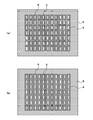
- one opening pattern 3 may be formed as shown in FIG. 2A, and a plurality of the opening patterns 3 are formed as shown in FIG. An opening pattern 3 may be formed.
- the film 4 is irradiated with the laser beam L1 with reference to a reference mark (for example, an alignment mark) formed in advance on the mask member 1 on the XY stage 9 on which the mask member 1 is placed in an XY two-dimensional direction. This is performed by step-shifting by a predetermined distance.
- a reference mark for example, an alignment mark
- the mask member 1 is positioned and placed on a reference substrate disposed on the XY stage 9 and provided with a reference mark that is an irradiation target of the laser beam L1, and the laser beam L1 is irradiated toward the reference mark. May be.
- the reference mark is positioned in the through hole 6 of the metal sheet 5 while observing the surface of the reference substrate with the camera through the film 4.
- the member 1 and the reference substrate are aligned.
- the reference mark is detected by the camera through the film 4 and, for example, the position coordinates of the reference mark with the initial position of the camera as the origin are calculated. .
- the reference substrate may be, for example, an organic EL display substrate, and the reference mark may be an anode electrode provided in advance on the substrate.
- the laser processing is not limited to the one performed by moving the XY stage 9, and may be performed by moving the illumination optical system side of the laser processing apparatus.
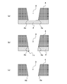
- FIG. 3 is a cross-sectional view for explaining the effect of the method for manufacturing a film formation mask according to the present invention.
- the laser processing rate of the support layer 2 is smaller than the laser processing rate of the film 4, or when the support layer 2 is a photosensitive resin that is not laser processed, as shown in FIG. It can function as a stopper for laser processing.
- the support layer 2 has only the surface violated or not processed at all. ) Is not likely to be laser processed.
- the back surface of the film 4 corresponding to the edge 3a of the opening pattern 3 is backed by the support layer 2, the generation
- the support layer 2 may also be subjected to the penetration processing after the opening pattern 3 has been penetrated into the film 4.
- the burr 11 is generated only at the edge of the through hole of the support layer 2, and is not generated at the edge 3 a of the opening pattern 3 of the film 4.
- the burr 11 of the support layer 2 does not affect the film formation mask.
- the completed film formation mask from which the support layer 2 has been removed has a burr on the edge 3a of the opening pattern 3 of the film 4, as shown in FIG. There is no occurrence, and favorable laser processing of the opening pattern 3 becomes possible.
- the fourth step is a step of removing the support layer 2 as shown in FIG.
- the support layer 2 is selectively removed from the film 4 by being dissolved in a solvent, a stripping solution or an etching solution.
- the support layer 2 may be selectively removed from the film 4 by chemical dry etching.
- polyimide as the film 4 is insoluble in almost all organic solvents, but acrylic resin as the support layer 2 is soluble in organic solvents such as acetone, toluene, and xylene.
- organic solvents such as acetone, toluene, and xylene.
- Polycarbonate and polystyrene are soluble in aromatic and chlorinated solvents.
- a photoresist made mainly of photosensitive polyimide or epoxy resin is soluble in an organic solvent.
- a polymer containing a benzene ring such as polyimide is difficult to dry-etch with a reactive gas containing CH 4 , but an acrylic resin-based polymer with many oxygen atoms is easily dry-etched with the reactive gas. It is known that.
- acrylic resin and photosensitive resin are less likely to be laser-processed than, for example, polyimide used as the film 4, can suppress the generation of internal stress on the film 4, and can be selectively removed from the film 4. It is a material suitable for the support layer 2.
- the fourth step it is preferable to clean and remove smear generated by the laser ablation process of the film 4 simultaneously with the removal of the support layer 2.
- the film formation mask has a structure in which the film 4 and the metal sheet 5 are laminated has been described.
- the film formation mask is a frame of a magnetic metal material made of, for example, Invar or Invar alloy. It may include a frame.
- the frame is a mask member either before or after the second step, that is, between the first step and the second step, or between the second step and the third step. 1 is preferable.
- the following steps are performed.
- green to near-infrared pulsed laser light L ⁇ b> 2 is irradiated from the film 4 side to a plurality of positions on the peripheral portion of the mask member 1, and the metal sheet 5 is attached to the frame 10. Spot-welded to one end face 10a.
- a second step is performed in which a resin liquid 7 different from the film 4 is applied from the film 4 side to form the support layer 2 on the surface of the film 4.
- the frame 10 when the frame 10 is attached between the second process and the third process, it is performed as follows. First, after completion of the second step, as shown in FIG. 5A, the mask member 1 is shown in FIG. 5 with the metal sheet 5 side of the mask member 1 facing the one end face 10 a of the frame 10. A tension is applied in the direction of arrow F, and the frame 10 is stretched.
- the laser beam L ⁇ b> 2 is irradiated from the film 4 side to a plurality of positions on the peripheral portion of the mask member 1, and the metal sheet 5 is spot welded to the one end face 10 a of the frame 10. .
- the laser beam L ⁇ b> 1 is irradiated from the metal sheet 5 side, the film 4 is penetrated through the portion of the film 4 corresponding to the inside of the through hole 6 of the metal sheet 5, and the opening pattern 3.
- a third step of forming is performed.
- the support layer 2 is shown to Fig.6 (a).
- the support layer 2 may be applied on the metal sheet 5.
- the laser beam L1 is irradiated from the side opposite to the surface on which the support layer 2 of the mask member 1 is formed as shown in FIG.
- the opening pattern 3 is formed by penetrating the film 4 through the film 4.
- the film formation mask has a structure in which the film 4 and the metal sheet 5 are laminated has been described.
- the present invention is not limited to this, and the film formation mask includes the metal sheet 5. It may be a structure not provided with.
Landscapes
- Engineering & Computer Science (AREA)
- Chemical & Material Sciences (AREA)
- Mechanical Engineering (AREA)
- Plasma & Fusion (AREA)
- Physics & Mathematics (AREA)
- Optics & Photonics (AREA)
- Manufacturing & Machinery (AREA)
- Chemical Kinetics & Catalysis (AREA)
- Materials Engineering (AREA)
- Metallurgy (AREA)
- Organic Chemistry (AREA)
- Laser Beam Processing (AREA)
- Physical Vapour Deposition (AREA)
- Electroluminescent Light Sources (AREA)
Abstract
本発明は、レーザ加工可能な樹脂製フィルム4の表裏何れか一方の面に、前記フィルム4とは異なる樹脂材料から成り、可視光よりも波長の短いレーザ光L1を吸収する樹脂製のサポート層2を形成する工程と、前記フィルム4の前記サポート層2を形成した面とは反対側からレーザ光L1を照射して、該フィルム4を貫通する開口パターン3を形成する工程と、前記フィルム4に対して前記サポート層2を選択除去する工程と、を行うものである。これにより、開口パターンの縁部におけるバリの発生を簡単なプロセスで抑制する。
Description
本発明は、樹脂製フィルムに開口パターンを形成した成膜マスクの製造方法に関し、特に開口パターンの縁部におけるバリの発生を簡単なプロセスで抑制し得る成膜マスクの製造方法に係るものである。
従来の成膜マスクの製造方法は、樹脂製のフィルムの裏面に銅等の金属層を形成し、該金属層を形成した面とは反対側からレーザ光を上記フィルムに照射し、フィルムをアブレートして開口パターンを形成し、その後、上記金属層をフィルムからエッチングして除去するものとなっていた(例えば、特許文献1参照)。
このように、フィルムの裏面に金属層を設けたことにより、アブレーション処理でフィルムの裏面に空気が溜まるのを回避することができ、開口パターンの縁部にバリが発生するのを抑制することができる。
しかし、このような従来の成膜マスクの製造方法においては、完成品の成膜マスクとしては不要なものであり、開口パターンの形成後に取り除かれる金属層を、製造過程でフィルムの裏面にめっき、蒸着又はスパッタリング等により形成する必要があり、製造プロセスが複雑になるという問題があった。
また、フィルムの裏面に該フィルムとは異なる材料の金属層を形成するものとなっていたため、両者間の線膨張係数が異なるときには、フィルムには大きな内部応力(引張応力)が発生するおそれがあった。したがって、フィルムをアブレーション処理して正規の位置に開口パターンを形成した後、フィルムから金属層が除去されると、上記フィルムの内部応力が解放され、その結果、開口パターンの位置がずれるおそれがあった。
さらに、上記金属層を形成した裏面とは反対側のフィルム表面に貫通孔を形成したメタルシートが積層されている場合には、フィルムの裏面に上記金属層をめっき形成するとき、又は、上記金属層をエッチングにより除去するときに、フィルム表面のメタルシート上に、例えば樹脂製の保護層を形成する必要があり、製造プロセスがより複雑になるという問題があった。
上記問題を解決するためには、上記金属層としてフィルムと線膨張係数が近似した材料が望まれ、より好適には、メタルシートに比してエッチング性の高い材料が望まれる。しかしながら、このような金属材料の選択範囲は限られ、材料選択は極めて困難なものとなっていた。
そこで、本発明は、このような問題点に対処し、開口パターンの縁部におけるバリの発生を簡単なプロセスで抑制し得る成膜マスクの製造方法を提供することを目的とする。
上記目的を達成するために、本発明による成膜マスクの製造方法は、レーザ加工可能な樹脂製フィルムの表裏何れか一方の面に、前記フィルムとは異なる樹脂材料から成り、可視光よりも波長の短いレーザ光を吸収する樹脂製のサポート層を形成する工程と、前記フィルムの前記サポート層を形成した面とは反対側からレーザ光を照射して、該フィルムを貫通する開口パターンを形成する工程と、前記フィルムに対して前記サポート層を選択除去する工程と、を行うものである。
本発明によれば、樹脂製フィルムの一面に形成される、フィルムとは異なる樹脂材料から成るサポート層は、塗布形成することができ、サポート層の形成が容易である。また、サポート層は、フィルムと同様に樹脂製であるため、フィルムと線膨張係数の近似したサポート層の選択が容易である。さらには、フィルムは不溶であるが、サポート層は可溶な溶剤の選定が容易であるため、サポート層をフィルムに対して選択的に除去可能である。したがって、フィルムの裏面を金属層で裏打ちした従来技術と違って、簡単な製造プロセスにより開口パターンの縁部にバリが発生するのを抑制することができる。
以下、本発明の実施形態を添付図面に基づいて詳細に説明する。図1は本発明による成膜マスクの製造方法の一実施形態を断面で示す工程図である。この成膜マスクの製造方法は、樹脂製フィルムに開口パターンを形成した成膜マスクを製造するもので、マスク用部材1を形成する第1工程と、サポート層2を形成する第2工程と、開口パターン3を形成する第3工程と、サポート層2を除去する第4工程と、を含むものである。
上記第1工程は、図1(a)に示すように、レーザ加工可能な樹脂製のフィルム4と貫通孔6を形成したメタルシート5とを積層してマスク用部材1を形成する工程である。
詳細には、上記マスク用部材1は、次のようにして形成することができる。即ち、厚みが5μm~15μm程度の非感光性ポリイミド(以下、単に「ポリイミド」という)等の可視光を透過するフィルムシートに無電解めっき、蒸着又はスパッタリング等によりニッケル等の良電導性の金属材料から成るシード層を形成する段階と、シード層上にフォトレジストを30μm~50μm程度の厚みで塗布した後、フォトマスクを使用して露光し、現像して上記貫通孔6に対応させて島パターンを形成する段階と、島パターンの外側のシード層上に電気めっきにより、ニッケル又はニッケル合金等の磁性金属材料を析出させて上記フォトレジストと略同じ厚みを有するメタルシート5を形成する段階と、溶剤又はレジスト剥離液に溶解させて上記島パターンを除去した後、島パターンの下側のシード層を公知のニッケル等のエッチング液を使用して除去する段階と、を実施する。
又は、30μm~50μm程度の厚みを有するニッケル又はニッケル合金等の磁性金属材料の金属シートの一面にポリイミド等の樹脂液を5μm~15μm程度の厚みに塗布した後、200℃~300℃で焼成してフィルム4を形成する段階と、上記金属シートの他面にフォトレジストを塗布した後、フォトマスクを使用して露光し、現像してレジストマスクを形成する段階と、上記レジストマスクを使用して上記金属シートをエッチングし、金属シートを貫通する貫通孔6を設けてメタルシート5を形成する段階と、レジストマスクを溶剤又は剥離液に溶解させて除去する段階と、を実施してもよい。
なお、ポリイミドの線膨張係数は1.5×10⁻⁵/℃~5×10-5/℃であり、ニッケル又はニッケル合金の線膨張係数は1.0×10-5/℃~1.8×10-5/℃で、両者の線膨張係数は比較的近似している。したがって、フィルム4とメタルシート5とを積層した構造の成膜マスクにおいては、線膨張係数の差によりフィルム4に発生する内部応力を抑制する目的から、フィルム4として線膨張係数が金属に近いポリイミド(PI)を使用するのが望ましい。ただし、フィルム4の材料としては、ポリイミドに限定されるものではなく、ポリエチレンテレフタレート(PET)、ポリエーテルエーテルケトン(PEEK)等のレーザ加工(レーザアブレーション)可能な他の樹脂材料であってもよい。また、メタルシート5は、ニッケル又はニッケル合金に限られず、インバー又はインバー合金等の他の磁性金属材料であってもよい。
上記第2工程は、図1(b)に示すように、マスク用部材1のフィルム4面に、フィルム4とは異なる樹脂材料から成り、可視光よりも波長の短いレーザ光(以下、単に「レーザ光」という)を吸収する樹脂製のサポート層2を形成する工程である。
詳細には、塗布装置のステージ上にマスク用部材1を、フィルム4側を上にして載置した後、上記レーザ光によりアブレートされて加工可能な材料の樹脂液7、又はレーザ光の照射により物性が変化する材料の樹脂液7を例えばスプレー8により塗布し、これを乾燥させてサポート層2を形成する。
この場合、サポート層2がレーザ加工(レーザアブレーション)可能な樹脂材料から成るときには、サポート層2は、レーザ光による加工レートがフィルム4の加工レートと同等又はそれよりも低い高分子材料が望ましい。
より詳細には、サポート層2としては、使用する波長のレーザ光に対する光吸収率が上記フィルム4と同等か又はそれよりも低い材料が望ましく、上記フィルム4が例えばポリイミドである場合には、サポート層2は、ポリイミドよりも光吸収率が低い、例えばアクリル系のポリメチルメタクリレート(PMMA)等が望ましい。
サポート層2の樹脂材料としては、アクリル樹脂以外に、ポリカーボネート(PC)、ポリスチレン(PS)等であってもよい。しかし、これらの樹脂は、アクリル樹脂に比べても光吸収率が低く、レーザ光による加工レートが低い材料である。
線膨張係数は、前記したようにポリイミドが1.5×10⁻⁵/℃~5×10-5/℃であるのに対して、アクリル樹脂が4.5×10-5/℃~7×10-5/℃であり、両者は比較的近似している。したがって、ポリイミドのフィルム4に対してアクリル樹脂のサポート層2を適用した場合には、フィルム4に発生する内部応力を抑制することができる。因みに、ポリカーボネートの線膨張係数は約6.5×10-5/℃、ポリスチレンの線膨張係数は6×10-5/℃~8×10-5/℃である。
また、サポート層2は、レーザ光の照射により物性が変化する感光性材料であってもよい。この場合、サポート層2としては、エポキシ樹脂を主原料とするフォトレジストや、感光性ポリイミド等が使用可能である。これらの樹脂材料は、線膨張係数がフィルム4の材料である例えばポリイミドと同等であると共に、ポリイミドは不溶の有機溶剤に可溶である特徴を有する。したがって、このようなサポート層2は、後述の第4工程において、有機溶剤に溶解させて容易に除去することができる。
より好ましくは、フィルム4とサポート層2との間の線膨張係数の差によりフィルム4に発生する内部応力をより抑制するために、サポート層2の厚みは、フィルム4の厚みと同等又はそれ以下であるのが望ましい。
上記第3工程は、図1(c)に示すように、マスク用部材1の上記サポート層2を形成した面とは反対側からレーザ光L1を照射し、メタルシート5の上記貫通孔6内に対応したフィルム4の部分に該フィルム4を貫通させて開口パターン3を形成する工程である。
ここで使用するレーザは、波長が400nm以下のレーザ光を発生するもので、例えばKrF248nmのエキシマレーザや、1064nmの第3高調波(355nm)や第4高調波(266nm)のレーザ光を放射するYAGレーザである。
一般に、高分子材料は、レーザ光の波長が短いほど光吸収係数が高い。ポリイミドは、可視域以上で光吸収が急激に低下し、PMMAは、近紫外域以上で光吸収が急激に低下することが知られている。したがって、波長が248nm~355nmの範囲で、ポリイミドよりも光吸収率の低いPMMAは、サポート層2として好適な材料であると言える。
上記開口パターン3の形成は、レーザ加工装置を使用して、レーザ光L1の複数ショットにより行われる。このレーザ加工装置は、パルス発光するレーザから放出されるレーザ光L1をインテグレータ光学系により照度分布を均一化して、開口パターン3の形状に相似形の開口を有する遮光マスクを照明し、該遮光マスクの前記開口を通過したレーザ光L1を集光レンズによりメタルシート5の貫通孔6内のフィルム4に集光するようになっている。
上記メタルシート5の1つの貫通孔6内には、図2(a)に示すように、1つの上記開口パターン3が形成されてもよく、同図(b)に示すように、複数の上記開口パターン3が形成されてもよい。
上記フィルム4へのレーザ光L1の照射は、マスク用部材1に予め形成された基準マーク(例えばアライメントマーク)を基準にして、マスク用部材1を載置したXYステージ9をXYの二次元方向に所定距離だけステップ移動させて行われる。
又は、XYステージ9上に配置され、レーザ光L1の照射目標となる基準マークを設けた基準基板上にマスク用部材1を位置決めして載置し、上記基準マークを狙ってレーザ光L1を照射してもよい。この場合、フィルム4が可視光を透過するものである時には、フィルム4を透してカメラで基準基板の表面を観察しながら基準マークがメタルシート5の貫通孔6内に位置するようにマスク用部材1と基準基板とを位置合わせする。さらに、フィルム4を透してカメラで基準マークを検出し、例えばカメラの初期位置を原点とする基準マークの位置座標を算出した後、該位置座標にレーザ光L1の照射位置を定めて照射する。
なお、上記基準基板は、例えば有機EL表示用基板であり、基準マークは該基板上に予め設けられたアノード電極であってもよい。また、レーザ加工は、XYステージ9を移動して行うものに限られず、レーザ加工装置の照明光学系側を移動して行ってもよい。
図3は本発明による成膜マスクの製造方法の効果を説明する断面図である。サポート層2のレーザ加工レートの方がフィルム4のレーザ加工レートよりも小さいとき、又はサポート層2がレーザ加工されない感光性樹脂であるときには、同図(a)に示すように、サポート層2をレーザ加工のストッパとして機能させることができる。この場合、例えば、マスク用部材1を上記基準基板上に載置してレーザ加工したとしても、サポート層2は表面が犯されるだけか、全く加工されないため、基準基板の基準マーク(例えばアノード電極)がレーザ加工されるおそれがない。しかも、開口パターン3の縁部3aに対応したフィルム4の裏面はサポート層2により裏打ちされているため、バリの発生は抑制される。
一方、フィルム4のレーザ加工レートとサポート層2のレーザ加工レートとが近似しているときには、フィルム4に開口パターン3が貫通加工された後に、サポート層2も貫通加工されることもあり得る。しかし、この場合は、図3(b)に示すように、バリ11はサポート層2の貫通孔の縁部に発生するだけで、フィルム4の開口パターン3の縁部3aには発生しない。しかも、サポート層2は、後に取り除かれるものであるから、サポート層2のバリ11は、成膜マスクに何ら影響を及ぼすものではない。
このように、上記いずれの場合にも、サポート層2が除去された完成後の成膜マスクには、図3(c)に示すように、フィルム4の開口パターン3の縁部3aにバリの発生はなく、開口パターン3の良好なレーザ加工が可能となる。
上記第4工程は、図1(d)に示すように、サポート層2を除去する工程である。サポート層2は、溶剤又は剥離液若しくはエッチング液に溶解させてフィルム4に対して選択的に除去される。又は、サポート層2は、化学的なドライエッチングによりフィルム4に対して選択的に除去されてもよい。
フィルム4としての例えばポリイミドは、略全ての有機溶剤に対して不溶であるが、サポート層2としての例えばアクリル樹脂は、アセトン、トルエン、キシレン等の有機溶剤に可溶である。また、ポリカーボネートやポリスチレンは、芳香族、塩素化溶剤に可溶である。さらに、前述したように感光性ポリイミドや、エポキシ樹脂を主原料とするフォトレジストは、有機溶剤に可溶である。
また、一般に、例えばポリイミドのようなベンゼン環を含むポリマーは、CH4を含む反応性ガスによってはドライエッチングされ難いが、酸素原子の多いアクリル樹脂系のポリマーは上記反応性ガスによってドライエッチングされ易いということが知られている。
このように、例えばアクリル樹脂や感光性樹脂等は、フィルム4として使用される例えばポリイミドに比べてレーザ加工され難く、フィルム4に対する内部応力の発生を抑制でき、且つフィルム4に対する選択的除去性を有しており、サポート層2として好適な材料である。
第4工程においては、サポート層2の除去と同時に、フィルム4のレーザアブレーション処理により発生するスミアも洗浄して除去するのがよい。
上記実施形態においては、成膜マスクがフィルム4とメタルシート5とを積層した構造を有するものである場合について述べたが、成膜マスクは、例えばインバー又はインバー合金等から成る磁性金属材料の枠状のフレームを含むものであってもよい。
この場合、フレームは、第2工程の実施前、又は実施後の何れかにおいて、即ち、上記第1工程と第2工程との間、又は第2工程と第3工程との間においてマスク用部材1と接合されるとよい。
詳細には、第1工程と第2工程との間にフレームが取り付けられる場合には、次のようにして実施される。
先ず、第1工程終了後、図4(a)に示すように、マスク用部材1のメタルシート5側をフレーム10の一端面10aに対面させた状態で、マスク用部材1に同図に示す矢印F方向にテンションを加えてフレーム10に架張される。
先ず、第1工程終了後、図4(a)に示すように、マスク用部材1のメタルシート5側をフレーム10の一端面10aに対面させた状態で、マスク用部材1に同図に示す矢印F方向にテンションを加えてフレーム10に架張される。
次に、図4(b)に示すように、マスク用部材1の周縁部の複数個所にフィルム4側から、例えば緑色乃至近赤外のパルスレーザ光L2が照射され、メタルシート5がフレーム10の一端面10aにスポット溶接される。
次いで、図4(c)に示すように、フィルム4側から該フィルム4とは異なる樹脂液7が塗布されてフィルム4の表面にサポート層2を形成する第2工程が実施される。
また、フレーム10が第2工程と第3工程との間において取り付けられる場合には、次のようにして実施される。
先ず、第2工程終了後、図5(a)に示すように、マスク用部材1のメタルシート5側をフレーム10の一端面10aに対面させた状態で、マスク用部材1に同図に示す矢印F方向にテンションを加えてフレーム10に架張される。
先ず、第2工程終了後、図5(a)に示すように、マスク用部材1のメタルシート5側をフレーム10の一端面10aに対面させた状態で、マスク用部材1に同図に示す矢印F方向にテンションを加えてフレーム10に架張される。
次に、図5(b)に示すように、マスク用部材1の周縁部の複数個所にフィルム4側からレーザ光L2が照射され、メタルシート5がフレーム10の一端面10aにスポット溶接される。
次いで、図5(c)に示すように、メタルシート5側からレーザ光L1が照射され、メタルシート5の貫通孔6内に対応したフィルム4の部分に該フィルム4を貫通させて開口パターン3を形成する第3工程が実施される。
なお、上記実施形態においては、サポート層2がマスク用部材1のメタルシート5とは反対側のフィルム4表面に塗布される場合について説明したが、サポート層2は、図6(a)に示すように、メタルシート5上に塗布されてもよい。この場合には、レーザ光L1は、同図(b)に示すように、マスク用部材1のサポート層2を形成した面とは反対側から照射され、メタルシート5の貫通孔6内に対応したフィルム4の部分に該フィルム4を貫通させて開口パターン3が形成される。
また、以上の説明においては、成膜マスクがフィルム4とメタルシート5とを積層した構造を有するものである場合について述べたが、本発明はこれに限られず、成膜マスクは、メタルシート5を備えない構造であってもよい。
1…マスク用部材
2…サポート層
3…開口パターン
4…フィルム
5…メタルシート
6…貫通孔
10…フレーム
L1…レーザ光(開口パターン形成用)
2…サポート層
3…開口パターン
4…フィルム
5…メタルシート
6…貫通孔
10…フレーム
L1…レーザ光(開口パターン形成用)
Claims (9)
- レーザ加工可能な樹脂製フィルムの表裏何れか一方の面に、前記フィルムとは異なる樹脂材料から成り、可視光よりも波長の短いレーザ光を吸収する樹脂製のサポート層を形成する工程と、
前記フィルムの前記サポート層を形成した面とは反対側からレーザ光を照射して、該フィルムを貫通する開口パターンを形成する工程と、
前記フィルムに対して前記サポート層を選択除去する工程と、
を行うことを特徴とする成膜マスクの製造方法。 - 前記サポート層は、前記レーザ光によるアブレーション加工が可能な材料から成ることを特徴とする請求項1記載の成膜マスクの製造方法。
- 前記サポート層の前記レーザ光による加工レートは、前記フィルムの加工レートと同等又はそれよりも低いことを特徴とする請求項2記載の成膜マスクの製造方法。
- 前記サポート層は、前記レーザ光の照射により物性が変化する材料から成ることを特徴とする請求項1記載の成膜マスクの製造方法。
- 前記サポート層の厚みは、前記フィルムの厚みと同等又はそれよりも薄いことを特徴とする請求項1~4のいずれか1項に記載の成膜マスクの製造方法。
- 前記サポート層を選択除去する工程において、前記サポート層は、溶剤又は剥離液若しくはエッチング液に溶解させて除去されることを特徴とする請求項1~4のいずれか1項に記載の成膜マスクの製造方法。
- 前記サポート層を選択除去する工程において、前記サポート層は、化学的なドライエッチングにより除去されることを特徴とする請求項1~4のいずれか1項に記載の成膜マスクの製造方法。
- 前記サポート層を形成する工程の実施前に、前記開口パターンが未加工の前記フィルムの表裏何れか一方の面に前記開口パターンを内包する大きさの貫通孔を設けたメタルシートを積層してマスク用部材を形成することを特徴とする請求項1~4のいずれか1項に記載の成膜マスクの製造方法。
- 前記サポート層を形成する工程の実施前、又は実施後の何れかにおいて、前記メタルシートを枠状のフレームに架張して固定することを特徴とする請求項8記載の成膜マスクの製造方法。
Priority Applications (2)
| Application Number | Priority Date | Filing Date | Title |
|---|---|---|---|
| CN201680063845.2A CN108350561B (zh) | 2015-10-30 | 2016-10-14 | 成膜掩模的制造方法 |
| KR1020187014602A KR20180077197A (ko) | 2015-10-30 | 2016-10-14 | 성막 마스크의 제조 방법 |
Applications Claiming Priority (2)
| Application Number | Priority Date | Filing Date | Title |
|---|---|---|---|
| JP2015214330A JP6714995B2 (ja) | 2015-10-30 | 2015-10-30 | 成膜マスクの製造方法 |
| JP2015-214330 | 2015-10-30 |
Publications (1)
| Publication Number | Publication Date |
|---|---|
| WO2017073369A1 true WO2017073369A1 (ja) | 2017-05-04 |
Family
ID=58631429
Family Applications (1)
| Application Number | Title | Priority Date | Filing Date |
|---|---|---|---|
| PCT/JP2016/080537 Ceased WO2017073369A1 (ja) | 2015-10-30 | 2016-10-14 | 成膜マスクの製造方法 |
Country Status (5)
| Country | Link |
|---|---|
| JP (1) | JP6714995B2 (ja) |
| KR (1) | KR20180077197A (ja) |
| CN (1) | CN108350561B (ja) |
| TW (1) | TWI682825B (ja) |
| WO (1) | WO2017073369A1 (ja) |
Cited By (2)
| Publication number | Priority date | Publication date | Assignee | Title |
|---|---|---|---|---|
| WO2020031302A1 (ja) * | 2018-08-08 | 2020-02-13 | 堺ディスプレイプロダクト株式会社 | 蒸着マスク、蒸着マスクの製造方法、および有機半導体素子の製造方法 |
| CN112894159A (zh) * | 2021-01-13 | 2021-06-04 | 苏州品维电子科技有限公司 | 一种用于制作logo板材及logo的加工方法 |
Families Citing this family (5)
| Publication number | Priority date | Publication date | Assignee | Title |
|---|---|---|---|---|
| CN110997969A (zh) | 2017-08-31 | 2020-04-10 | 堺显示器制品株式会社 | 成膜掩模的制造方法 |
| JP7059839B2 (ja) * | 2018-07-11 | 2022-04-26 | 大日本印刷株式会社 | 蒸着マスクの製造方法、蒸着マスク製造装置、蒸着パターン形成方法、および有機半導体素子の製造方法 |
| CN112522958A (zh) * | 2019-09-18 | 2021-03-19 | 天守(福建)超纤科技股份有限公司 | 一种光影处理技术合成革及其制备方法 |
| CN113578064B (zh) * | 2021-08-03 | 2024-03-29 | 深圳通微新能源科技有限公司 | 一种去除相转移成型的膜的表面皮层的方法及膜制品 |
| JP2024009519A (ja) * | 2022-07-11 | 2024-01-23 | ウシオ電機株式会社 | 蒸着マスク製造方法 |
Citations (4)
| Publication number | Priority date | Publication date | Assignee | Title |
|---|---|---|---|---|
| JP2013108143A (ja) * | 2011-11-22 | 2013-06-06 | V Technology Co Ltd | マスクの製造方法及びマスクの製造装置 |
| JP2013165058A (ja) * | 2012-01-12 | 2013-08-22 | Dainippon Printing Co Ltd | 蒸着マスクの製造方法、及び有機半導体素子の製造方法 |
| JP2014121720A (ja) * | 2012-12-21 | 2014-07-03 | V Technology Co Ltd | 蒸着マスクの製造方法 |
| JP2014133938A (ja) * | 2013-01-11 | 2014-07-24 | Dainippon Printing Co Ltd | 蒸着マスクの製造方法、金属マスク付き樹脂層、及び有機半導体素子の製造方法 |
Family Cites Families (3)
| Publication number | Priority date | Publication date | Assignee | Title |
|---|---|---|---|---|
| JP3182301B2 (ja) * | 1994-11-07 | 2001-07-03 | キヤノン株式会社 | マイクロ構造体及びその形成法 |
| JPWO2009035036A1 (ja) * | 2007-09-14 | 2010-12-24 | コニカミノルタホールディングス株式会社 | 電極の形成方法及び有機薄膜トランジスタ |
| JP6331312B2 (ja) * | 2013-09-30 | 2018-05-30 | 大日本印刷株式会社 | 蒸着マスクの製造方法、及び蒸着マスク準備体 |
-
2015
- 2015-10-30 JP JP2015214330A patent/JP6714995B2/ja not_active Expired - Fee Related
-
2016
- 2016-10-14 KR KR1020187014602A patent/KR20180077197A/ko not_active Withdrawn
- 2016-10-14 WO PCT/JP2016/080537 patent/WO2017073369A1/ja not_active Ceased
- 2016-10-14 CN CN201680063845.2A patent/CN108350561B/zh active Active
- 2016-10-27 TW TW105134678A patent/TWI682825B/zh active
Patent Citations (4)
| Publication number | Priority date | Publication date | Assignee | Title |
|---|---|---|---|---|
| JP2013108143A (ja) * | 2011-11-22 | 2013-06-06 | V Technology Co Ltd | マスクの製造方法及びマスクの製造装置 |
| JP2013165058A (ja) * | 2012-01-12 | 2013-08-22 | Dainippon Printing Co Ltd | 蒸着マスクの製造方法、及び有機半導体素子の製造方法 |
| JP2014121720A (ja) * | 2012-12-21 | 2014-07-03 | V Technology Co Ltd | 蒸着マスクの製造方法 |
| JP2014133938A (ja) * | 2013-01-11 | 2014-07-24 | Dainippon Printing Co Ltd | 蒸着マスクの製造方法、金属マスク付き樹脂層、及び有機半導体素子の製造方法 |
Cited By (4)
| Publication number | Priority date | Publication date | Assignee | Title |
|---|---|---|---|---|
| WO2020031302A1 (ja) * | 2018-08-08 | 2020-02-13 | 堺ディスプレイプロダクト株式会社 | 蒸着マスク、蒸着マスクの製造方法、および有機半導体素子の製造方法 |
| JP6671572B1 (ja) * | 2018-08-08 | 2020-03-25 | 堺ディスプレイプロダクト株式会社 | 蒸着マスク、蒸着マスクの製造方法、および有機半導体素子の製造方法 |
| CN112543817A (zh) * | 2018-08-08 | 2021-03-23 | 堺显示器制品株式会社 | 蒸镀掩模、蒸镀掩模的制造方法以及有机半导体元件的制造方法 |
| CN112894159A (zh) * | 2021-01-13 | 2021-06-04 | 苏州品维电子科技有限公司 | 一种用于制作logo板材及logo的加工方法 |
Also Published As
| Publication number | Publication date |
|---|---|
| JP2017082313A (ja) | 2017-05-18 |
| JP6714995B2 (ja) | 2020-07-01 |
| TW201726289A (zh) | 2017-08-01 |
| CN108350561A (zh) | 2018-07-31 |
| KR20180077197A (ko) | 2018-07-06 |
| CN108350561B (zh) | 2020-07-17 |
| TWI682825B (zh) | 2020-01-21 |
Similar Documents
| Publication | Publication Date | Title |
|---|---|---|
| JP6714995B2 (ja) | 成膜マスクの製造方法 | |
| KR102137223B1 (ko) | 성막 마스크의 제조 방법 | |
| JP6898998B2 (ja) | 電磁放射及び続くエッチングプロセスにより材料内に少なくとも1つの空隙を施すための方法 | |
| JP5958804B2 (ja) | 蒸着マスク、蒸着マスクの製造方法及び有機el表示装置の製造方法 | |
| JP6035548B2 (ja) | 蒸着マスク | |
| JP7171059B2 (ja) | 電子部品の製造方法 | |
| JP6123301B2 (ja) | 蒸着マスクの製造方法、金属マスク付き樹脂層、及び有機半導体素子の製造方法 | |
| WO2015115136A1 (ja) | 成膜マスクの製造方法及び成膜マスク | |
| JP2017179591A (ja) | 成膜マスク、その製造方法及び成膜マスクのリペア方法 | |
| JP6163376B2 (ja) | 成膜マスクの製造方法及び成膜マスク | |
| JP6078746B2 (ja) | 蒸着マスクの製造方法 | |
| JP2018053345A (ja) | メタルマスクの製造方法 | |
| CN105023848B (zh) | 基板结构的制造方法及基板结构 | |
| WO2017170172A1 (ja) | 成膜マスク、その製造方法及び成膜マスクのリペア方法 | |
| JP6304425B2 (ja) | 蒸着マスクの製造方法、金属マスク付き樹脂層、及び有機半導体素子の製造方法 | |
| JP2007088187A (ja) | レジストパターンの形成方法およびその利用 | |
| JP2021163893A (ja) | 回路配線基板および配線パターン形成方法 | |
| US8420301B2 (en) | Method for forming a wiring pattern by laser irradiation | |
| JP6497596B2 (ja) | 蒸着マスク装置の中間体 | |
| CN111180328A (zh) | 用于制造掩模的基底蚀刻方法 | |
| TWI384324B (zh) | 圖案化膜層的製造方法 | |
| JP2018056455A (ja) | 基板の製造方法 | |
| JP5993270B2 (ja) | レーザ加工方法 | |
| TW202417161A (zh) | 盲孔加工方法 |
Legal Events
| Date | Code | Title | Description |
|---|---|---|---|
| 121 | Ep: the epo has been informed by wipo that ep was designated in this application |
Ref document number: 16859599 Country of ref document: EP Kind code of ref document: A1 |
|
| NENP | Non-entry into the national phase |
Ref country code: DE |
|
| ENP | Entry into the national phase |
Ref document number: 20187014602 Country of ref document: KR Kind code of ref document: A |
|
| 122 | Ep: pct application non-entry in european phase |
Ref document number: 16859599 Country of ref document: EP Kind code of ref document: A1 |