WO2017061072A1 - p型シリコンウェーハ中のFe濃度測定方法 - Google Patents
p型シリコンウェーハ中のFe濃度測定方法 Download PDFInfo
- Publication number
- WO2017061072A1 WO2017061072A1 PCT/JP2016/004049 JP2016004049W WO2017061072A1 WO 2017061072 A1 WO2017061072 A1 WO 2017061072A1 JP 2016004049 W JP2016004049 W JP 2016004049W WO 2017061072 A1 WO2017061072 A1 WO 2017061072A1
- Authority
- WO
- WIPO (PCT)
- Prior art keywords
- measurement
- spv
- concentration
- time
- light
- Prior art date
- Legal status (The legal status is an assumption and is not a legal conclusion. Google has not performed a legal analysis and makes no representation as to the accuracy of the status listed.)
- Ceased
Links
Images
Classifications
-
- G—PHYSICS
- G01—MEASURING; TESTING
- G01R—MEASURING ELECTRIC VARIABLES; MEASURING MAGNETIC VARIABLES
- G01R31/00—Arrangements for testing electric properties; Arrangements for locating electric faults; Arrangements for electrical testing characterised by what is being tested not provided for elsewhere
- G01R31/26—Testing of individual semiconductor devices
- G01R31/2648—Characterising semiconductor materials
-
- H—ELECTRICITY
- H10—SEMICONDUCTOR DEVICES; ELECTRIC SOLID-STATE DEVICES NOT OTHERWISE PROVIDED FOR
- H10P—GENERIC PROCESSES OR APPARATUS FOR THE MANUFACTURE OR TREATMENT OF DEVICES COVERED BY CLASS H10
- H10P74/00—Testing or measuring during manufacture or treatment of wafers, substrates or devices
- H10P74/20—Testing or measuring during manufacture or treatment of wafers, substrates or devices characterised by the properties tested or measured, e.g. structural or electrical properties
- H10P74/207—Electrical properties, e.g. testing or measuring of resistance, deep levels or capacitance-voltage characteristics
-
- G—PHYSICS
- G01—MEASURING; TESTING
- G01R—MEASURING ELECTRIC VARIABLES; MEASURING MAGNETIC VARIABLES
- G01R31/00—Arrangements for testing electric properties; Arrangements for locating electric faults; Arrangements for electrical testing characterised by what is being tested not provided for elsewhere
- G01R31/26—Testing of individual semiconductor devices
- G01R31/265—Contactless testing
- G01R31/2656—Contactless testing using non-ionising electromagnetic radiation, e.g. optical radiation
-
- H—ELECTRICITY
- H10—SEMICONDUCTOR DEVICES; ELECTRIC SOLID-STATE DEVICES NOT OTHERWISE PROVIDED FOR
- H10P—GENERIC PROCESSES OR APPARATUS FOR THE MANUFACTURE OR TREATMENT OF DEVICES COVERED BY CLASS H10
- H10P74/00—Testing or measuring during manufacture or treatment of wafers, substrates or devices
- H10P74/23—Testing or measuring during manufacture or treatment of wafers, substrates or devices characterised by multiple measurements, corrections, marking or sorting processes
- H10P74/235—Testing or measuring during manufacture or treatment of wafers, substrates or devices characterised by multiple measurements, corrections, marking or sorting processes comprising optical enhancement of defects or not-directly-visible states
-
- H—ELECTRICITY
- H10—SEMICONDUCTOR DEVICES; ELECTRIC SOLID-STATE DEVICES NOT OTHERWISE PROVIDED FOR
- H10P—GENERIC PROCESSES OR APPARATUS FOR THE MANUFACTURE OR TREATMENT OF DEVICES COVERED BY CLASS H10
- H10P74/00—Testing or measuring during manufacture or treatment of wafers, substrates or devices
- H10P74/20—Testing or measuring during manufacture or treatment of wafers, substrates or devices characterised by the properties tested or measured, e.g. structural or electrical properties
- H10P74/203—Structural properties, e.g. testing or measuring thicknesses, line widths, warpage, bond strengths or physical defects
Definitions
- the present invention relates to a method for measuring Fe concentration in a p-type silicon wafer by the SPV method (Surface Photo-Voltage).
- SPV measurement a p-type silicon wafer is irradiated with light of a specific wavelength, the surface electromotive force (SPV signal) of the wafer at that time is measured, and the diffusion length of minority carriers in the wafer is obtained.
- SPV measurement this is also simply referred to as “SPV measurement”.
- the SPV method is an excellent method capable of non-contact and non-destructive measurement as well as a shorter measurement time than other methods.
- SPV measurement has two types of measurement modes: Standard Mode and Ultimate Mode.
- Standard mode is a general method in which SPV measurement using a certain wavelength is performed, and then SPV measurement using another wavelength is sequentially performed.
- Ultimate mode is a special method that irradiates multiple types of light with different wavelengths in the same time and performs SPV measurement at once.
- Patent Document 1 measurement can be completed in a shorter time by performing measurement in Ultimate mode, so measurement errors in the minority carrier diffusion length due to environmental changes over time during measurement are measured. It is stated that it can be made smaller. A smaller measurement error of the minority carrier diffusion length means that the lower detection limit of the Fe concentration can be lowered.
- Ultimate Mode was examined. Due to the difference in measurement method, it is certain that Ultimate Mode is easier to shorten the time required for measurement than Standard Mode. However, according to the study by the present inventors, the measurement time can naturally be shortened only by changing the measurement mode from Standard Mode to Ultimate Mode, but contrary to the description in Patent Document 1, detection of Fe concentration is possible. It has been found that the lower limit cannot be lowered, but rather the lower limit of detection of the Fe concentration is increased.
- the present invention provides a method for measuring Fe concentration in a p-type silicon wafer by the SPV method, which can lower the detection limit of Fe concentration and perform measurement in a short time. Objective.
- Patent Document 1 only describes that an error in the diffusion length of minority carriers becomes small if measurement is performed in UltimateUMode, and no consideration is given to optimizing other setting parameters.
- the present inventors first changed the measurement parameters in the standard mode recommended by the manufacturer of the SPV apparatus based on the case where the measurement parameters were set to known values that were also recommended by the manufacturer. Then, in Standard ⁇ ⁇ mode, it was found that a parameter called Number of Readings, which will be described later, greatly affects the lower limit of Fe concentration detection. In other words, the lower the Fe concentration detection limit, the lower the Number of Readings. However, an increase in Number of Readings means an increase in the time required for measurement. In this way, regardless of how the measurement parameters are set in Standard mode, the lower detection limit of Fe concentration can be lowered under long measurement time conditions, but the lower detection limit of Fe concentration can be increased under short measurement time conditions. Met. That is, in Standard mode, it was impossible to achieve both reduction of the measurement time and reduction of the Fe concentration detection lower limit.
- the present inventors found that the following knowledge was found when various measurement parameters were changed in the case of Ultimate mode.
- Ultimate ⁇ mode basically, the lower detection limit of Fe concentration was low under the condition where the measurement time was long, and the lower detection limit of Fe concentration was high under the condition where the measurement time was short.
- Ultimate mode is easy to shorten the time required for measurement, so if the measurement parameter satisfies the specific condition in Ultimate ⁇ ⁇ ⁇ ⁇ ⁇ mode, the measurement parameter in Standard mode is the above known value (recommended by the manufacturer of SPV device) It was found that the lower limit of detection of the Fe concentration can be lowered and the time required for the measurement can be shortened as compared with the case of the above condition.
- the gist of the present invention is as follows. (1) In determining the Fe concentration in the silicon wafer based on the measurement by the SPV method performed on the p-type silicon wafer, The measurement uses a measurement mode that irradiates light of multiple different wavelengths in the same period. Time Between Readings is 35 ms to 120 ms and Time Constant is 20 ms or more, or Time Between Readings is 10 ms to 35 m. A method for measuring Fe concentration in a p-type silicon wafer, characterized in that the measurement is performed under conditions of less than a second, Time Constant of 100 ms or more, and Number of Readings of 12 times or less.
- the lower limit of detection of Fe concentration can be lowered and measurement can be performed in a short time.
- One embodiment of the present invention relates to a method for obtaining an Fe concentration in a silicon wafer based on a measurement by a SPV method (SPV measurement) performed on a p-type silicon wafer.
- SPV measurement SPV measurement
- Fe existing in the p-type silicon wafer is combined with a dopant (for example, boron) by an electrostatic force to form an Fe—B pair.
- a dopant for example, boron
- Fe is separated from B.
- the minority carrier diffusion length obtained as a result of SPV measurement means the distance that can be moved before the minority carriers generated by the light irradiated during SPV measurement disappear. This minority carrier is trapped by the trap level formed by Fe in the wafer, for example, and disappears.
- Levels formed by Fe in a p-type silicon wafer include Fe-B (iron boron pair) that normally exists and Fei (interstitial iron) formed by light irradiation. Each trap level has a different ease of capturing minority carriers. For this reason, Fe is more likely to trap minority carriers and the diffusion length is smaller in the dissociated state than in the normal state. Using this difference, the Fe concentration in the wafer can be determined as follows.
- a map of Fe concentration in the wafer can be obtained by performing SPV measurement in a normal state and a dissociated state at a plurality of locations on the wafer surface.
- the processing for separating the Fe—B pair is a conventional method and is not particularly limited, and examples thereof include irradiation with a flash lamp.
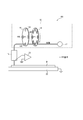
- FIG. 1 is a schematic diagram illustrating an example of the configuration of an analog SPV measurement apparatus 100.
- the SPV measuring apparatus 100 includes an optical module 10, a probe 18, a lock-in amplifier 20, and a stage 22.
- the optical module 10 includes a light source 12, a chopper 14, and a filter wheel 16.
- the light source 12 is, for example, a white LED, and an optical path is set so that light emitted from the light source 12 is irradiated onto the surface of the wafer W placed on the stage 22.
- the chopper 14 is a disk member having a plurality of holes in a circumferential shape, and gives a frequency to the light emitted from the light source 12 by rotating. That is, light is intermittently applied to the surface of the wafer W.
- the frequency of light given here is defined as “chopping frequency (CF)” and is one of the measurement parameters. CF is usually set to about 500 to 3000 Hz.
- the filter wheel 16 is provided with a filter that allows only different wavelengths of light to pass through each of the holes 16A to 16D, whereby the surface of the wafer W can be irradiated with light of a specific wavelength.
- FIG. 1 shows the case where the optical module 10 is an analog type, but it may be a digital type.
- the digital type a plurality of single color LEDs having different emission wavelengths are modularized, and each LED is blinked, whereby light of a specific wavelength can be irradiated on the surface of the wafer W at a specific frequency.
- the wavelength of the irradiation light is not particularly limited as long as it is a plurality of wavelengths between 780 nm and 1004 nm.
- a combination of 780 nm and 1004 nm can be exemplified.
- a combination of 780 nm, 914 nm, 975 nm, and 1004 nm can be exemplified.
- the intensity (light quantity) of the irradiation light is set as Injection Level and is one of the measurement parameters.
- the light amount of Level 2 is 2 ⁇ 10 12 (atoms / cc)
- the light amount of Level 3 is 3 ⁇ 10 12 (atoms / cc).
- the probe 18 has a capacitance sensor at the tip, and always measures the capacitance generated between the surface of the wafer W and the probe 18.
- the surface of the wafer W Prior to SPV measurement, the surface of the wafer W is subjected to HF treatment, and the surface is positively charged.
- minority carriers (electrons because they are p-type) are generated in the wafer and move toward the positively charged surface.
- the electrons reach the surface, they cancel each other out with the positive charge on the surface, so that the surface potential is lowered and, as a result, the capacitance is also lowered.
- the difference in capacitance at this time is detected as an SPV signal. The more electrons trapped by Fe in the wafer, the lower the surface potential.
- the lock-in amplifier 20 amplifies and detects the SPV signal corresponding to the capacitance measured by the probe 18. In this way, an SPV signal can be obtained. By moving the stage 22, SPV measurement can be performed at a plurality of locations in the wafer W plane.
- SPV device examples include known SPV devices such as FAaST330 manufactured by Semilab-SDi LLC and SPV-Station-1020 manufactured by StrategicDiagnostics.
- SPV measurement is performed using light having a first wavelength (for example, 780 nm), and an SPV signal corresponding to the light is obtained.
- first wavelength for example, 780 nm
- SPV signal corresponding to the light
- the “penetration length” depending on the wavelength of the irradiation light is taken on the X axis and the “light quantity / SPV signal” is taken on the Y axis, and the measurement results are plotted.
- SPV measurement is performed using light having a second wavelength (for example, 1004 nm) different from the first wavelength, and an SPV signal corresponding to the light is obtained. Similarly, the measurement results are plotted.
- the X-intercept when the two plots obtained in this way are connected by a straight line can be defined as the “diffusion length”. Note that when SPV measurement is performed at three or more types of wavelengths, three or more plots are obtained. Therefore, an X intercept is obtained by an approximation process such as a least square method.
- Standard Mode SPV measurement using a certain wavelength is performed, and then SPV measurement using another wavelength is sequentially performed. Therefore, the above plots are sequentially obtained.
- Ultimate mode light of a plurality of different wavelengths is irradiated during the same period and SPV measurement is performed at one time, so the above plot can be obtained by one measurement.
- SPV signals having different frequencies can be obtained in the lock-in amplifier 20 by making the chopping frequency of light different for each wavelength, so that SPV signals corresponding to the respective wavelengths can be obtained separately.
- Number ofReadings (hereinafter referred to as “NR”) means the number of SPV signal acquisitions in one SPV measurement.
- Time Constant hereinafter referred to as “TC”) means the acquisition time of the SPV signal for each acquisition time.
- Time Between Readings (hereinafter referred to as “TB”) means a time interval (standby time) of each acquisition.
- the average value of these 12 SPV signals is used as the SPV signal corresponding to the light of the first wavelength. Thereafter, the light of the second wavelength (for example, 1004 nm) to which CF: 1600 ⁇ 100 Hz is applied is irradiated for the predetermined time, and then the SPV signal is acquired for 20 msec, and then the standby time is set to 20 msec. This is repeated 12 times to obtain 12 SPV signals. The average value of these 12 SPV signals is used as the SPV signal corresponding to the light of the second wavelength.
- CF 1600 ⁇ 100Hz
- light quantity Level 3
- NR 12 times
- TC 20ms
- TB 20ms
- the first wavelength for example, 780 nm
- the second wavelength for example, 1004 nm
- the SPV signal is acquired for 20 msec.
- the standby time is set to 20 msec. This is repeated 12 times to obtain 12 SPV signals.
- the SPV signal corresponding to the light of the first wavelength and the SPV signal corresponding to the light of the second wavelength are obtained separately, so that the average value of each SPV signal is obtained as the light of each wavelength. Is used as an SPV signal corresponding to.
- the lower limit of detection of the Fe concentration is 1.0 ⁇ 10 9 / cm 3 , and the time required for measuring one wafer is 28 minutes. Met.
- the detection limit of Fe concentration is less than 1.0 ⁇ 10 9 / cm 3 and the time required for measuring one wafer is less than 28 minutes, The result was not able to be obtained.
- the detection limit of Fe concentration is less than 1.0 ⁇ 10 9 / cm 3 , and 1
- the time required to measure one wafer was less than 28 minutes. Therefore, in one embodiment of the present invention, it is important to perform SPV measurement in the Ultimate mode under the following conditions.
- TB is set to 35 msec or more and 120 msec or less and TC is set to 20 msec or more (first condition), or TB is set to 10 msec or more and less than 35 msec and TC is set to 100 msec or more (second condition).
- first condition the sum of TB and TC is 40 milliseconds, whereas in one embodiment of the present invention, the sum of TB and TC is at least 55 milliseconds or more.
- the detection lower limit of the Fe concentration can be reduced by increasing TB and / or TC as compared with the conventional case.
- the present inventors presume the reason for such a result as follows.
- the total amount of light irradiated onto the wafer at a time is doubled compared to the case of Standard mode, so that the wafer W is easily heated by light irradiation.
- the sum of TB and TC that is, the length of time during which no light is irradiated
- an increase in the temperature of the wafer W during reading of the SPV signal can be suppressed. It is considered that the lower limit of detection of Fe concentration can be reduced.
- the detection limit of Fe concentration cannot be reduced if TC is less than 20 ms. Moreover, even if TC is 20 milliseconds or more and less than 100 milliseconds, if TB is less than 35 milliseconds, the detection limit of Fe concentration cannot be reduced. When TB exceeds 120 milliseconds, not only the time required for measurement of one wafer is lengthened, but also the Fe-B repairing progresses, so that the lower limit of detection of the Fe concentration is also increased. Therefore, the first condition is necessary.
- the detection limit of Fe concentration cannot be reduced if the TC is less than 100 milliseconds. Moreover, even if TC is 100 milliseconds or more, if TB is less than 10 milliseconds, the lower limit of detection of Fe concentration cannot be reduced.
- the upper limit of TC is preferably set to 1000 milliseconds. When TC exceeds 1000 milliseconds, not only the time required for measurement of one wafer is lengthened, but also the Fe-B repairing progresses, so that the lower limit of detection of Fe concentration is also increased.
- NR shall be 12 times or less. This is because if the NR exceeds 12 times, the time required for measuring one wafer becomes longer. Note that, under the above first or second conditions, a sufficient detection sensitivity of Fe concentration could be obtained even with one NR.
- Example 1 Standard mode
- a FAaST330 manufactured by Semilab-SDi LLC was used as an SPV apparatus, the CF was fixed at 1584 Hz, the light intensity was fixed at Level 3, and the NR, TC, TB were various values shown in Table 1, and SPV measurement was performed in Standard mode.
- the irradiation wavelengths were 780 nm and 1004 nm.
- the lower limit of detection of the Fe concentration was determined by the following method.
- a boron-doped p-type silicon wafer in which the Fe—B pair was dissociated was prepared based on the description in JP-A-2011-054784, and SPV measurement was performed on nine points in the surface of the wafer after HF treatment.
- the minority carrier diffusion length obtained here was treated as the minority carrier diffusion length L FeB in the normal state.
- the silicon wafer was irradiated with a flash lamp 12 times at intervals of 5 seconds, and then waited for 5 minutes. Thereafter, SPV measurement was again performed at nine points in the plane, and the diffusion length L Fei of minority carriers in the dissociated state was determined.
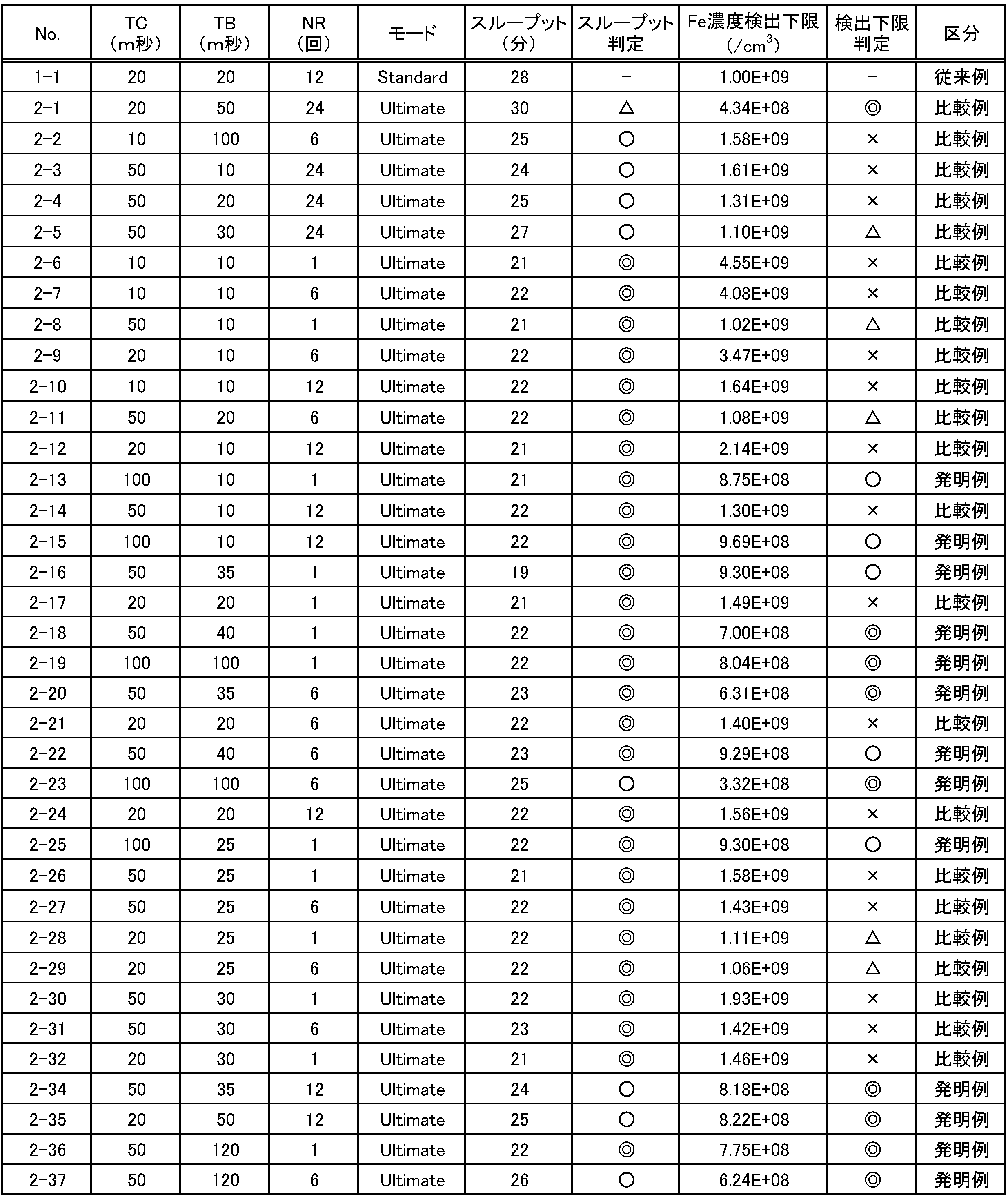
- the throughput was obtained by the following method. Diffusion lengths L FeB and L Fei are calculated for the 177 points in the surface of the boron-doped p-type silicon wafer by the same method as in the previous paragraph, and the Fe concentration [Fe] at the 177 points in the surface is calculated based on the above formula. And an Fe concentration map was obtained. At this time, the time required from loading to unloading of the wafer was defined as “throughput”, and the results are shown in Table 1. Note that the column of “throughput determination” in Table 1 is based on the following criteria. ⁇ : 15% or more shorter than conventional example ⁇ : Less than 15% shorter than conventional example ⁇ : Less than 15% longer than conventional example ⁇ : 15% or more shorter than conventional example
- the lower limit of detection of Fe concentration can be lowered and measurement can be performed in a short time.
Landscapes
- Physics & Mathematics (AREA)
- General Physics & Mathematics (AREA)
- Health & Medical Sciences (AREA)
- Electromagnetism (AREA)
- Toxicology (AREA)
- Testing Or Measuring Of Semiconductors Or The Like (AREA)
- Investigating Or Analysing Materials By Optical Means (AREA)
Abstract
Description
(1)p型シリコンウェーハに対して行うSPV法による測定に基づいて、該シリコンウェーハ中のFe濃度を求めるにあたり、
前記測定は、互いに異なる複数種類の波長の光を同期間に照射する測定モードにより、Time Between Readingsを35m秒以上120m秒以下かつTime Constantを20m秒以上、または、Time Between Readingsを10m秒以上35m秒未満かつTime Constantを100m秒以上とし、Number of Readingsを12回以下とする条件下にて行うことを特徴とする、p型シリコンウェーハ中のFe濃度測定方法。
[Fe]=C×(1/LFei - 1/LFeB)
ただし、Cは定数である。
Semilab-SDi LLC製のFAaST330をSPV装置として用い、CFは1584Hz、光量はLevel 3で固定し、NR,TC,TBを表1に示す種々の値として、Standard modeでSPV測定を行った。照射波長は、780nmと1004nmとした。
◎:従来例よりも15%以上の低下
○:従来例よりも15%未満の低下
△:従来例よりも15%未満の増加
×:従来例よりも15%以上の増加
◎:従来例よりも15%以上の短縮
○:従来例よりも15%未満の短縮
△:従来例よりも15%未満の延長
×:従来例よりも15%以上の延長

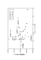
Semilab-SDi LLC製のFAaST330をSPV装置として用い、CF1は1584Hz、CF2は1634Hzとし、光量はLevel 3で固定し、NR,TC,TBを表2に示す種々の値として、Ultimate modeでSPV測定を行った。照射波長は、780nmと1004nmとした。実験例1と同様の手法で、Fe濃度の検出下限とスループットを求め、結果を表2に示した。判定結果も同様の基準で表2に示した。また、表2の測定結果から、Fe濃度の検出下限とスループットとの関係も図2に合わせて示した。
10 光モジュール
12 光源
14 チョッパー
16 フィルターホイール
18 プローブ
20 ロックインアンプ
22 ステージ
W シリコンウェーハ
Claims (1)
- p型シリコンウェーハに対して行うSPV法による測定に基づいて、該シリコンウェーハ中のFe濃度を求めるにあたり、
前記測定は、互いに異なる複数種類の波長の光を同期間に照射する測定モードにより、Time Between Readingsを35m秒以上120m秒以下かつTime Constantを20m秒以上、または、Time Between Readingsを10m秒以上35m秒未満かつTime Constantを100m秒以上とし、Number of Readingsを12回以下とする条件下にて行うことを特徴とする、p型シリコンウェーハ中のFe濃度測定方法。
Priority Applications (5)
| Application Number | Priority Date | Filing Date | Title |
|---|---|---|---|
| US15/765,792 US10871515B2 (en) | 2015-10-07 | 2016-09-05 | Method of measuring Fe concentration in p-type silicon wafer |
| CN201680058320.XA CN108140592B (zh) | 2015-10-07 | 2016-09-05 | p型硅晶圆中的Fe浓度测量方法 |
| JP2017544172A JP6458874B2 (ja) | 2015-10-07 | 2016-09-05 | p型シリコンウェーハ中のFe濃度測定方法 |
| KR1020187009570A KR102007191B1 (ko) | 2015-10-07 | 2016-09-05 | p형 실리콘 웨이퍼 중의 Fe 농도 측정 방법 |
| DE112016004633.2T DE112016004633B4 (de) | 2015-10-07 | 2016-09-05 | VERFAHREN ZUM MESSEN DER Fe-KONZENTRATION IN EINEM P-TYP-SILIZIUMWAFER |
Applications Claiming Priority (2)
| Application Number | Priority Date | Filing Date | Title |
|---|---|---|---|
| JP2015199589 | 2015-10-07 | ||
| JP2015-199589 | 2015-10-07 |
Publications (1)
| Publication Number | Publication Date |
|---|---|
| WO2017061072A1 true WO2017061072A1 (ja) | 2017-04-13 |
Family
ID=58488284
Family Applications (1)
| Application Number | Title | Priority Date | Filing Date |
|---|---|---|---|
| PCT/JP2016/004049 Ceased WO2017061072A1 (ja) | 2015-10-07 | 2016-09-05 | p型シリコンウェーハ中のFe濃度測定方法 |
Country Status (7)
| Country | Link |
|---|---|
| US (1) | US10871515B2 (ja) |
| JP (1) | JP6458874B2 (ja) |
| KR (1) | KR102007191B1 (ja) |
| CN (1) | CN108140592B (ja) |
| DE (1) | DE112016004633B4 (ja) |
| TW (1) | TWI616965B (ja) |
| WO (1) | WO2017061072A1 (ja) |
Cited By (3)
| Publication number | Priority date | Publication date | Assignee | Title |
|---|---|---|---|---|
| WO2019123767A1 (ja) * | 2017-12-22 | 2019-06-27 | 株式会社Sumco | p型シリコンウェーハ中のFe濃度測定方法及びSPV測定装置 |
| JP2019114658A (ja) * | 2017-12-22 | 2019-07-11 | 株式会社Sumco | p型シリコンウェーハ中のFe濃度測定方法及びSPV測定装置 |
| JP2019114662A (ja) * | 2017-12-22 | 2019-07-11 | 株式会社Sumco | p型シリコンウェーハ中のFe濃度測定方法及びSPV測定装置 |
Citations (2)
| Publication number | Priority date | Publication date | Assignee | Title |
|---|---|---|---|---|
| JP2005277417A (ja) * | 2004-03-22 | 2005-10-06 | Kla Tencor Technologies Corp | 試料の1つ又は複数の特性を決定するための方法とシステム |
| JP2007053123A (ja) * | 2005-08-15 | 2007-03-01 | Sumco Corp | シリコンウェーハ表面の安定化判定方法およびシリコンウェーハの製造方法 |
Family Cites Families (11)
| Publication number | Priority date | Publication date | Assignee | Title |
|---|---|---|---|---|
| JP2815251B2 (ja) | 1991-06-26 | 1998-10-27 | 株式会社日立ビルシステム | エレベータの主索交換方法 |
| JP2843815B2 (ja) * | 1992-08-12 | 1999-01-06 | 住友シチックス株式会社 | BドープP型Si中のFe濃度測定方法 |
| JPH0864650A (ja) * | 1994-08-24 | 1996-03-08 | Komatsu Electron Metals Co Ltd | Fe−B濃度測定によるシリコンウェーハの評価方法 |
| AU2001281291A1 (en) | 2000-06-29 | 2002-01-14 | Semiconductor Diagnostics, Inc. | Method for fast and accurate determination of the minority carrier diffusion length from simultaneously measured surface photovoltages |
| US20040010394A1 (en) * | 2002-07-15 | 2004-01-15 | Seh America, Inc. | Systems, methods and computer program products for determining contaminant concentrations in semiconductor materials |
| JP4416566B2 (ja) * | 2004-04-26 | 2010-02-17 | Sumco Techxiv株式会社 | 不純物金属濃度測定の方法 |
| US8093920B2 (en) * | 2008-10-06 | 2012-01-10 | Semiconductor Diagnostics, Inc. | Accurate measuring of long steady state minority carrier diffusion lengths |
| JP5556090B2 (ja) | 2009-09-02 | 2014-07-23 | 株式会社Sumco | ボロンドープp型シリコン中の鉄濃度分析における定量分析限界決定方法 |
| JP5545131B2 (ja) | 2010-08-27 | 2014-07-09 | 株式会社Sumco | ボロンドープp型シリコン中の鉄濃度分析における定量分析限界決定方法 |
| JP5659632B2 (ja) | 2010-08-27 | 2015-01-28 | 株式会社Sumco | ボロンドープp型シリコンウェーハの鉄濃度分析方法および分析装置、シリコンウェーハ、ならびにシリコンウェーハの製造方法 |
| CN106505004B (zh) * | 2015-09-07 | 2019-05-03 | 中芯国际集成电路制造(上海)有限公司 | 检测晶圆中铁含量异常的装置及其方法 |
-
2016
- 2016-09-05 CN CN201680058320.XA patent/CN108140592B/zh active Active
- 2016-09-05 JP JP2017544172A patent/JP6458874B2/ja active Active
- 2016-09-05 WO PCT/JP2016/004049 patent/WO2017061072A1/ja not_active Ceased
- 2016-09-05 KR KR1020187009570A patent/KR102007191B1/ko active Active
- 2016-09-05 US US15/765,792 patent/US10871515B2/en active Active
- 2016-09-05 DE DE112016004633.2T patent/DE112016004633B4/de active Active
- 2016-09-30 TW TW105131554A patent/TWI616965B/zh active
Patent Citations (2)
| Publication number | Priority date | Publication date | Assignee | Title |
|---|---|---|---|---|
| JP2005277417A (ja) * | 2004-03-22 | 2005-10-06 | Kla Tencor Technologies Corp | 試料の1つ又は複数の特性を決定するための方法とシステム |
| JP2007053123A (ja) * | 2005-08-15 | 2007-03-01 | Sumco Corp | シリコンウェーハ表面の安定化判定方法およびシリコンウェーハの製造方法 |
Cited By (9)
| Publication number | Priority date | Publication date | Assignee | Title |
|---|---|---|---|---|
| WO2019123767A1 (ja) * | 2017-12-22 | 2019-06-27 | 株式会社Sumco | p型シリコンウェーハ中のFe濃度測定方法及びSPV測定装置 |
| JP2019114658A (ja) * | 2017-12-22 | 2019-07-11 | 株式会社Sumco | p型シリコンウェーハ中のFe濃度測定方法及びSPV測定装置 |
| JP2019114662A (ja) * | 2017-12-22 | 2019-07-11 | 株式会社Sumco | p型シリコンウェーハ中のFe濃度測定方法及びSPV測定装置 |
| KR20200039720A (ko) | 2017-12-22 | 2020-04-16 | 가부시키가이샤 사무코 | p형 실리콘 웨이퍼 중의 Fe 농도 측정 방법 및 SPV 측정 장치 |
| CN111771268A (zh) * | 2017-12-22 | 2020-10-13 | 胜高股份有限公司 | p型硅晶片中的Fe浓度测定方法和SPV测定装置 |
| US11387151B2 (en) | 2017-12-22 | 2022-07-12 | Sumco Corporation | Method of measuring concentration of Fe in p-type silicon wafer and SPV measurement apparatus |
| KR102425872B1 (ko) * | 2017-12-22 | 2022-07-27 | 가부시키가이샤 사무코 | p형 실리콘 웨이퍼 중의 Fe 농도 측정 방법 및 SPV 측정 장치 |
| CN111771268B (zh) * | 2017-12-22 | 2024-02-20 | 胜高股份有限公司 | p型硅晶片中的Fe浓度测定方法和SPV测定装置 |
| US12107018B2 (en) | 2017-12-22 | 2024-10-01 | Sumco Corporation | Method of measuring concentration of Fe in p-type silicon wafer and SPV measurement apparatus |
Also Published As
| Publication number | Publication date |
|---|---|
| DE112016004633B4 (de) | 2025-12-31 |
| DE112016004633T5 (de) | 2018-06-21 |
| TWI616965B (zh) | 2018-03-01 |
| JP6458874B2 (ja) | 2019-01-30 |
| TW201727790A (zh) | 2017-08-01 |
| CN108140592B (zh) | 2022-08-02 |
| US20180284182A1 (en) | 2018-10-04 |
| JPWO2017061072A1 (ja) | 2018-02-22 |
| KR20180050374A (ko) | 2018-05-14 |
| CN108140592A (zh) | 2018-06-08 |
| KR102007191B1 (ko) | 2019-08-05 |
| US10871515B2 (en) | 2020-12-22 |
Similar Documents
| Publication | Publication Date | Title |
|---|---|---|
| JP5682858B2 (ja) | シリコンウェーハの評価方法および製造方法 | |
| JP2014239230A5 (ja) | ||
| JP6458874B2 (ja) | p型シリコンウェーハ中のFe濃度測定方法 | |
| CN102144284A (zh) | 用于缺陷检测的方法及设备 | |
| JP2015101529A (ja) | シリコン単結晶の炭素濃度測定方法 | |
| TW201642343A (zh) | 電漿處理裝置及電漿處理方法 | |
| TWI611489B (zh) | 半導體基板的評估方法及半導體基板的製造方法 | |
| US8093920B2 (en) | Accurate measuring of long steady state minority carrier diffusion lengths | |
| JP2015059858A (ja) | 半導体の抵抗率検査装置および半導体の抵抗率検査方法 | |
| WO2010113232A1 (ja) | 検査方法及び検査装置 | |
| JP5712778B2 (ja) | Soiウェーハのsoi層の膜厚測定方法 | |
| US20060066324A1 (en) | Method for measuring impurity metal concentration | |
| US20070273400A1 (en) | Apparatus and Method for Electrical Characterization of Semiconductors | |
| JP5638098B2 (ja) | 検査装置、及び検査条件取得方法 | |
| JP2017084985A (ja) | 結晶欠陥の位置特定方法、結晶欠陥観察用試料の作製方法、及び結晶欠陥の評価方法 | |
| JP6344168B2 (ja) | ボロンドープp型シリコンウェーハの金属汚染評価方法および評価装置、ならびにボロンドープp型シリコンウェーハの製造方法 | |
| JP6848849B2 (ja) | p型シリコンウェーハ中のFe濃度測定方法及びSPV測定装置 | |
| JP6844561B2 (ja) | 酸素濃度評価方法 | |
| TWI646323B (zh) | 矽晶材檢測方法及其檢測裝置 | |
| JP6848850B2 (ja) | p型シリコンウェーハ中のFe濃度測定方法及びSPV測定装置 | |
| JP6458612B2 (ja) | 半導体ウェーハの製造方法および半導体ウェーハの評価方法 | |
| RU2537104C2 (ru) | Способ разделения интегральных схем по надежности | |
| JP6785642B2 (ja) | 少数キャリア寿命評価方法および少数キャリア寿命評価装置 | |
| JP2015070116A (ja) | ウエーハの評価方法 | |
| JP2019056625A (ja) | 欠陥サイズ分布の測定方法 |
Legal Events
| Date | Code | Title | Description |
|---|---|---|---|
| 121 | Ep: the epo has been informed by wipo that ep was designated in this application |
Ref document number: 16853231 Country of ref document: EP Kind code of ref document: A1 |
|
| ENP | Entry into the national phase |
Ref document number: 2017544172 Country of ref document: JP Kind code of ref document: A |
|
| ENP | Entry into the national phase |
Ref document number: 20187009570 Country of ref document: KR Kind code of ref document: A |
|
| WWE | Wipo information: entry into national phase |
Ref document number: 15765792 Country of ref document: US |
|
| WWE | Wipo information: entry into national phase |
Ref document number: 112016004633 Country of ref document: DE |
|
| 122 | Ep: pct application non-entry in european phase |
Ref document number: 16853231 Country of ref document: EP Kind code of ref document: A1 |
|
| WWG | Wipo information: grant in national office |
Ref document number: 112016004633 Country of ref document: DE |