WO2017047909A1 - 導電性複合材料及びその製造方法{conductive composite material and manufacturing method thereof} - Google Patents
導電性複合材料及びその製造方法{conductive composite material and manufacturing method thereof} Download PDFInfo
- Publication number
- WO2017047909A1 WO2017047909A1 PCT/KR2016/006297 KR2016006297W WO2017047909A1 WO 2017047909 A1 WO2017047909 A1 WO 2017047909A1 KR 2016006297 W KR2016006297 W KR 2016006297W WO 2017047909 A1 WO2017047909 A1 WO 2017047909A1
- Authority
- WO
- WIPO (PCT)
- Prior art keywords
- electrode
- composite material
- conductive composite
- metal
- item
- Prior art date
- Legal status (The legal status is an assumption and is not a legal conclusion. Google has not performed a legal analysis and makes no representation as to the accuracy of the status listed.)
- Ceased
Links
Images


Classifications
-
- H—ELECTRICITY
- H01—ELECTRIC ELEMENTS
- H01B—CABLES; CONDUCTORS; INSULATORS; SELECTION OF MATERIALS FOR THEIR CONDUCTIVE, INSULATING OR DIELECTRIC PROPERTIES
- H01B1/00—Conductors or conductive bodies characterised by the conductive materials; Selection of materials as conductors
-
- H—ELECTRICITY
- H01—ELECTRIC ELEMENTS
- H01B—CABLES; CONDUCTORS; INSULATORS; SELECTION OF MATERIALS FOR THEIR CONDUCTIVE, INSULATING OR DIELECTRIC PROPERTIES
- H01B1/00—Conductors or conductive bodies characterised by the conductive materials; Selection of materials as conductors
- H01B1/20—Conductive material dispersed in non-conductive organic material
- H01B1/22—Conductive material dispersed in non-conductive organic material the conductive material comprising metals or alloys
-
- H—ELECTRICITY
- H01—ELECTRIC ELEMENTS
- H01B—CABLES; CONDUCTORS; INSULATORS; SELECTION OF MATERIALS FOR THEIR CONDUCTIVE, INSULATING OR DIELECTRIC PROPERTIES
- H01B1/00—Conductors or conductive bodies characterised by the conductive materials; Selection of materials as conductors
- H01B1/20—Conductive material dispersed in non-conductive organic material
- H01B1/24—Conductive material dispersed in non-conductive organic material the conductive material comprising carbon-silicon compounds, carbon or silicon
-
- H—ELECTRICITY
- H01—ELECTRIC ELEMENTS
- H01B—CABLES; CONDUCTORS; INSULATORS; SELECTION OF MATERIALS FOR THEIR CONDUCTIVE, INSULATING OR DIELECTRIC PROPERTIES
- H01B13/00—Apparatus or processes specially adapted for manufacturing conductors or cables
-
- H—ELECTRICITY
- H01—ELECTRIC ELEMENTS
- H01B—CABLES; CONDUCTORS; INSULATORS; SELECTION OF MATERIALS FOR THEIR CONDUCTIVE, INSULATING OR DIELECTRIC PROPERTIES
- H01B5/00—Non-insulated conductors or conductive bodies characterised by their form
- H01B5/14—Non-insulated conductors or conductive bodies characterised by their form comprising conductive layers or films on insulating-supports
-
- H—ELECTRICITY
- H05—ELECTRIC TECHNIQUES NOT OTHERWISE PROVIDED FOR
- H05B—ELECTRIC HEATING; ELECTRIC LIGHT SOURCES NOT OTHERWISE PROVIDED FOR; CIRCUIT ARRANGEMENTS FOR ELECTRIC LIGHT SOURCES, IN GENERAL
- H05B33/00—Electroluminescent light sources
- H05B33/10—Apparatus or processes specially adapted to the manufacture of electroluminescent light sources
-
- H—ELECTRICITY
- H05—ELECTRIC TECHNIQUES NOT OTHERWISE PROVIDED FOR
- H05B—ELECTRIC HEATING; ELECTRIC LIGHT SOURCES NOT OTHERWISE PROVIDED FOR; CIRCUIT ARRANGEMENTS FOR ELECTRIC LIGHT SOURCES, IN GENERAL
- H05B33/00—Electroluminescent light sources
- H05B33/12—Light sources with substantially two-dimensional [2D] radiating surfaces
- H05B33/14—Light sources with substantially two-dimensional [2D] radiating surfaces characterised by the chemical or physical composition or the arrangement of the electroluminescent material, or by the simultaneous addition of the electroluminescent material in or onto the light source
-
- H—ELECTRICITY
- H05—ELECTRIC TECHNIQUES NOT OTHERWISE PROVIDED FOR
- H05B—ELECTRIC HEATING; ELECTRIC LIGHT SOURCES NOT OTHERWISE PROVIDED FOR; CIRCUIT ARRANGEMENTS FOR ELECTRIC LIGHT SOURCES, IN GENERAL
- H05B33/00—Electroluminescent light sources
- H05B33/12—Light sources with substantially two-dimensional [2D] radiating surfaces
- H05B33/26—Light sources with substantially two-dimensional [2D] radiating surfaces characterised by the composition or arrangement of the conductive material used as an electrode
- H05B33/28—Light sources with substantially two-dimensional [2D] radiating surfaces characterised by the composition or arrangement of the conductive material used as an electrode of translucent electrodes
Definitions
- the present invention relates to a conductive composite material, an electrode using the same, and a method for manufacturing the same, and more specifically, an electrode using a conductive composite material including a metal nanowire, a method for manufacturing the electrode, and an electrode
- the present invention relates to an element to be used.
- the resistance of the ITO electrode is high, and there is a limit to enlargement of the display.
- durability is low, such as cracking of the electrode and disconnection.
- indium is a rare metal and the supply amount is small, and the production cost of ITO electrodes is high.
- a method using a conductive polymer (PEDOT: PSS) as a transparent electrode for a flexible display has also been proposed, but because the polymer itself has high resistance and absorbs visible light, it does not have high transparency. There is a limit to the application to the display.
- electrodes using metal powder and metal nanowires have been studied.
- An electrode can be formed by applying a metal nanoparticle dispersion containing metal powder or metal nanowires to a substrate.
- Silver powder is easy to synthesize in large quantities and has the advantage of being easy to use in various industries such as electrode wiring and other printing processes. This can cause problems such as peeling in subsequent manufacturing processes.
- the contact resistance between the metal particles in the powder is very large, the electrical characteristics are reduced compared to the case where the metal is in a bulk state, and the electrode is formed with fine particles having a size of several tens of nanometers or less.
- an additional baking process using a laser or high temperature is necessary.
- metal nanoparticles are evaporated at a low temperature of almost 200 ° C. or lower, and phase changes occur.
- the present invention is to solve the above-described problems of the prior art, and an object of the present invention is to provide a conductive composite material including a metal nanostructure and a metal paste, and a method for manufacturing the same. Another object of the present invention is to provide an electrode having improved electrical and mechanical characteristics using a novel conductive composite material and a method for producing the same. Another object of the present invention is to use a novel conductive composite material for a printed circuit board (PCB), a flexible circuit board (FPC), a radio frequency identification (RFID) tag antenna, a conductive ink used for electromagnetic wave shielding, etc.
- PCB printed circuit board
- FPC flexible circuit board
- RFID radio frequency identification
- the present invention provides an electrode material used for materials, plasma display (PDP), liquid crystal display, organic light emitting element, flexible display, and electromagnetic wave shielding agent.
- the conductive composite material according to the present invention includes a metal nanostructure and a metal component, and the metal component is selected from the group consisting of metal particles, a carbon-based conductor, and a conductive polymer.
- the electrode according to the present invention is formed by filling a recess formed in a substrate containing a permeable material with a conductive composite material.
- the device according to the present invention is formed by filling a recess formed in a flexible substrate with a conductive composite material.
- the method for manufacturing an electrode according to the present invention includes a step of filling a conductive composite material into a recess formed in a substrate including a transmissive material, and a step of pressure-bonding the conductive composite material.
- the conductive composite material according to the present invention has improved electrical conductivity characteristics and adhesion to the substrate, and various physical properties can be selected according to the application by adjusting the shape, viscosity, solid content, etc. of the nanostructures contained therein. Can be adjusted.
- the electrode according to the invention has a high electrical conductivity, is uniform throughout the electrode and has a high mechanical flexibility.
- the substrate provided with the electrode according to the present invention can maintain a stable current flow without breaking the electrode even when the substrate is bent.
- the electrode manufacturing method according to the present invention facilitates miniaturization of the electrode, can maintain the height of the electrode constant, and can have translucency.
- FIG. 1 is a schematic diagram for explaining a manufacturing process of a transparent electrode having a pattern according to the present invention.
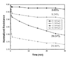
- FIG. 2 is a result of measuring a change in resistance value depending on a processing time during a baking process by immersing a thin film formed of the conductive composite material of Example 1 according to the present invention in an aqueous NaCl solution having various concentrations.
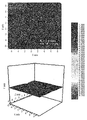
- FIG. 3 shows the result of measuring the resistance at each position on the thin film of Example 8 according to the present invention and measuring the average resistance value and the non-uniformity of resistance.
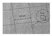
- FIG. 4A shows Example 9 according to the present invention.
- 4 (b) is a photograph of an electron microscope in which the intersection of the electrodes in Example 9 is enlarged
- FIG. 4 (c) is a diagram showing the conductivity filled in the recesses in Example 9. It is the photograph of the electron microscope which expanded the property composite material.
- FIG. 5 shows the results of measuring the light transmission characteristics of Examples 9 and 10 according to the present invention.
- the conductive composite material according to the present invention can be manufactured by mixing a metal nanostructure in a certain ratio with a conductive paste.
- the conductive paste of the present invention may contain all or part of a solvent, a binder and a dispersion material together with conductive particles.
- Including conductive particles which may include, but are not limited to, metal particles, carbon-based conductors, and conductive polymers.
- the conductive particles according to the present invention may include, but are not limited to, particles made of Ag, Au, Cu, Ni, Co, or Al.
- the carbon-based conductor according to the present invention may include conductive carbon black, graphite, or carbon nanotube.
- the conductive polymer according to the present invention may include polypyrrole, polyaniline, polythiophene, or a derivative thereof.
- the conductive paste according to the present invention may be a thermosetting type, an ultraviolet curable type, an osmotic drying type, or a solvent volatile type paste, and at least one of a thermoplastic resin, a crosslinkable resin, and a polyester resin depending on the type. One can be included.
- the paste according to the present invention may contain 50% by mass or more of silver particles, 10% by mass or more of a polyester resin, and may contain 10 to 50% by mass of a pyrolytic silver salt.
- the ratio of the silver paste which is a kind of the conductive paste according to the present invention, is preferably 2 to 5, and particularly preferably 2.5 to 3.
- the viscosity of the silver paste according to the present invention is preferably 800 mPa ⁇ s to 400,000 mPa ⁇ s, more preferably 10,000 mPa ⁇ s to 100,000 mPa ⁇ s, measured using an HB type viscometer. However, it is not limited to this.
- the silver particle size in the silver paste according to the present invention may have a size from 100 nm to 10 ⁇ m, and may be 1 ⁇ m to 5 ⁇ m, but is not limited thereto.
- the metal nanostructure of the present invention can have a nanoparticle or a silver nanowire structure, but preferably has a metal nanostructure silver nanowire structure.
- the material of the metal nanostructure of the present invention may be formed of one or more materials selected from the group consisting of Ag, Au, Cu, Ni, Co, and Al, but is not limited thereto.
- the metal nanostructure of the present invention can have a nanoparticle or a silver nanowire structure, but preferably has a metal nanostructure silver nanowire structure.
- the material of the metal nanostructure of the present invention may be formed of one or more materials selected from the group consisting of Ag, Au, Cu, Ni, Co, and Al, but is not limited thereto.
- the silver nanowire according to the present invention can be manufactured by various methods, but it is preferable to manufacture by reducing metal ions with a solvent in which a halogen compound and a dispersant are dissolved. Moreover, after forming a silver nanowire, the desalting process can be performed and the stability of a wire can be maintained.
- halogen compounds used for the production of silver nanowires are compounds containing bromine, chlorine, and iodine, and include alkali halides such as sodium bromide, sodium chloride, and sodium iodide depending on the purpose. Can be used.
- a polymer having a hydrophilic group such as polymer in gelatin, polyvinyl alcohol (P-3), methylhydroxy, polyalkyleneamine, or the like can be preferably used as a polymer.
- the polymer used as the dispersant those having a weight average molecular weight of 3,000 to 30,000 can be used.
- a single substance that functions as a dispersant and a halogen compound, for example, HTAB containing an amino group and a hydrate ion may be used.
- the solvent that can be used for the production of silver nanowires is a hydrophilic solvent, and water, alcohols, ethers, ketones and the like can be used alone or in combination.
- the average major axis length of the silver nanowire according to the present invention is 0.1 to 500 ⁇ m, preferably 1 to 150 ⁇ m, and more preferably 10 to 50 ⁇ m.
- the average minor axis length of the silver nanowire is 1 to 300 nm, preferably 5 to 150 nm, but is not limited thereto.
- the coefficient of variation of the short axis length of the wire is preferably 40% or less, more preferably 30% or less, and the coefficient of variation is a predetermined number. It is calculated
- the cross section of the silver nanowire may be a circle, an ellipse, or a polygon. In order to ensure high transparency so that it can be used for a display, a circle or a polygon of pentagon or more is preferable.
- the polarity between the solvent in the conductive paste and the solvent of the dispersion of the metal nanostructure Depending on the difference, precipitation or agglomeration of solid content may occur.
- the solvent of the conductive paste and the metal nanostructure dispersion liquid are mixed in such a ratio that no solid content is generated.
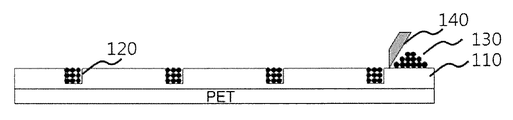
- FIG. 1 is a schematic view illustrating a manufacturing process of a transparent electrode having a pattern according to an embodiment of the present invention.
- a part of the substrate (110) is removed to form a recess (120), and a conductive composite material (120) according to the present invention is applied thereon, so that the recess (120) is filled with the conductive composite material.
- the substrate (110) may be made of a translucent material, but is not limited thereto.
- the blade (140) is swept across the surface of the substrate to remove the conductive composite material outside the recesses of the substrate.
- a predetermined pressure is applied to the blade (140) against the substrate to crimp the conductive composite material in the recess so that the conductive composite material is uniformly disposed in the recess. Characteristics can be improved.
- electrode patterns can be formed by methods such as screen printing, gravure printing, gravure offset printing, and ink jet printing.
- the recesses of the present invention can be formed on the substrate at intervals of 50 ⁇ m to 500 ⁇ m, and can be formed periodically, preferably 100 ⁇ m to 300 ⁇ m.
- the width of the recess can be 1 to 10 ⁇ m, preferably 3 to 7 ⁇ m.
- the depth of the recess can be 1 to 10 ⁇ m, preferably 2 to 5 ⁇ m.
- the cross section of the concave portion is not limited to the quadrangle shown in FIG. 1, but may be a polygon and a figure including a curve in part.
- the shape of the recesses according to the present invention and the interval between them can be modified according to the purpose of use.
- post-treatment such as applying heat at a predetermined temperature, performing a chemical baking process, or applying light such as laser, infrared, or ultraviolet light A process can be performed.
- a post-treatment step can be performed in the atmosphere, an inert gas atmosphere, or a vacuum state.
- heat treatment can be performed at a temperature of 80 ° C. to 200 ° C., preferably 100 ° C. to 150 ° C., more preferably 80 ° C. as a post-treatment step.
- Heat treatment is performed at ⁇ 120 ° C.
- the heat treatment can be performed in two stages, a low temperature and a high temperature.
- the second heat treatment can be performed after the first heat treatment is performed for 30 minutes at a temperature of 150 to 200 ° C.
- a chemical baking process can be performed as one of the post-processing steps for the thin film or pattern of the conductive composite material in the air or in a solution.
- the chemical baking treatment can be performed by immersing the conductive composite material in a solution containing an electrolyte substance.
- the electrolyte material according to the present invention may be selected from the group consisting of MgCl 2 , HCl, LiCl, NaCl, MgSO 4 , and FeSO 4 , but is not limited thereto, and a material that can remove the polymer capping agent is used.
- a chemical baking treatment By such a chemical baking treatment, the polymer capping agent remaining in the solvent of the conductive paste and the dispersion of the metal nanostructure can be removed, and the resistance of the electrode made of the conductive composite material is low. Thus, the resistance with respect to the entire electrode becomes uniform, and the electrical characteristics are improved.
- a step of washing the electrode with water and performing a drying treatment at a predetermined temperature can be performed.
- the drying conditions can be adjusted according to the use of the electrode.
- a graphene or ITO layer may be additionally formed thereon.
- the electrode manufactured according to the present invention may have a light transmittance of 75% or more, and can be 90% or more by process optimization.
- the sheet resistance of the electrode may be 10 ⁇ / ⁇ or less, preferably 5 ⁇ / ⁇ or less, and more preferably 3 ⁇ / ⁇ or less by a post-treatment step such as firing.
- a display employing an electrode having a high light transmittance and a low sheet resistance has a large ratio (aperture ratio) of pixels in the device, and a uniform electrical signal from the electrode wiring can be stably transmitted. Therefore, for example, when light is emitted by applying an electric current to an organic light emitting layer having a corner length of 10 cm or more using such an electrode, each region can emit light uniformly.
- the device manufactured by forming the electrode of the present invention on the substrate is flexible even if the shape of the electrode is changed by bending or winding the device itself, the electrode is not disconnected, and the electrical conduction state does not change. .
- a flexible or bendable organic light emitting display, an organic light emitting illumination device, or the like can be realized by using the electrode on a flexible or bendable substrate.
- the present invention will be described in more detail through examples and comparative examples. However, it should be clarified that the following examples and comparative examples are provided for illustrative purposes only to facilitate understanding of the present invention, and that the scope and scope of the present invention are not limited thereto.
- Examples 1 to 4 of the present invention are thin-film electrodes manufactured using a conductive composite material manufactured by changing the mixing ratio of the metal nanostructure and the metal paste.
- the dispersion of the metal nanostructure used in the production of this example was a silver nanowire dispersion from N & B.
- the solvent of the dispersion is isopropyl alcohol, the length of the silver nanowire is 20 ⁇ m, and the thickness is 40 nm.
- the silver paste used in the manufacture of the examples of the present invention is ICP 1427 of Changson Co., Ltd.
- the silver particles contained have a size of 1 um and 3 um, and the viscosity is about 16,200 cps.
- Example 9 is a patterned electrode manufactured by filling the conductive composite material of Example 1 into a PET substrate having a recess having a width of 5 ⁇ m and a depth of 3 ⁇ m.
- Example 10 is an electrode in which an ITO film having a thickness of 20 nm is formed over the entire pattern-type electrode of Example 9.
- FIG. 2 is a result of measuring the change in resistance value according to the baking time when the thin film formed of the conductive composite material of Example 1 was immersed in various concentrations of NaCl aqueous solution and fired. . As the concentration of the NaCl aqueous solution increases, the resistance value decreases more. In the case of the thin film of Example 8 that is baked at 5.0 M NaCl concentration for 30 minutes, the resistance can be decreased by 26.8%.
- FIG. 3 shows the results of measuring the resistance at each position of the thin film of Example 8 and measuring the average resistance value and the nonuniformity. The resistance non-uniformity is measured as 17.2%, which reduces the resistance non-uniformity by about 46% compared to Example 1 without chemical baking.
- FIG. 4A is a photograph of a microscope of Example 9
- FIG. 4B is a photograph of an electron microscope in which a region where electrode recesses intersect is enlarged
- FIG. It is the photograph of the electron microscope which expanded the electrically conductive composite material of this.
- the conductive composite material is densely filled in the recess, the shape of the electrode formed as the conductive composite material in the recess is uniform, and therefore the resistance of the electrode is also low. It can be kept constant throughout the substrate.
- FIG. 5 shows the measurement of the light transmission characteristics of Examples 9 and 10.
- Examples 9 and 10 have a transmittance of 80% or more in the entire region of the visible light. In particular, Example 9 has a transmittance of 90 days. % Isanim is confirmed.
- Substrate 120 Recess 130: Conductive composite material 140: Blade
Landscapes
- Physics & Mathematics (AREA)
- Spectroscopy & Molecular Physics (AREA)
- Engineering & Computer Science (AREA)
- Manufacturing & Machinery (AREA)
- Chemical & Material Sciences (AREA)
- Dispersion Chemistry (AREA)
- Non-Insulated Conductors (AREA)
- Conductive Materials (AREA)
- Electroluminescent Light Sources (AREA)
Abstract
本発明は、導電性複合材料と、これを用いた電極及びその製造方法に関するもので、電気伝導度が高く、電極全体にわたって抵抗値が均一であり、高い機械的柔軟性を有しながら、微細化にも有利であり、ディスプレイなどの電子装置の透明電極に適用することができる。特に、本発明の電極はフレキシブルやベンダブルディスプレイや照明装置の電極として用いることができる。
Description
本発明は、導電性複合材料と、これを用いた電極及びその製造方法に関するものであり、さらに具体的には、金属ナノワイヤを含む導電性複合材料を用いた電極、その製造方法及びその電極を利用する素子に関するものである。
最近、電気、電子素子分野、特にディスプレイ分野において、透明電極に関する需要及び関心が高まっている。
最近、ディスプレイの大型化、軽量化とともに装置のフレキシブル(flexible)やベンダブル(bendable)化が求められている。最近、有機発光素子(organic light−emitting devices)を用いた電子素子、ディスプレイの商用化により、このような要求がさらに大きくなっている。このようなフレキシブルやベンダブルディスプレイの製造には、十分に柔軟性のある基板だけでなく、基板上に形成される電極も柔軟性を有さなければならず、基板の変形によっても電極の導電性が弱まってはならない。
ディスプレイの電極としては、主に酸化インジウムスズ(ITO,Indium Tin Oxide)を用いた透明電極が用いられているが、ITO電極の抵抗が高く、ディスプレイの大型化に限界があり、フレキシブル基板にITO電極を形成した後、曲げると電極にクラックが生じ、断線が発生する等の耐久性が低い問題がある。さらに、インジウムが稀少金属として供給量が少なく、ITO電極の生産単価も高い。
フレキシブルディスプレイ用の透明電極として導電性ポリマー(PEDOT:PSS)を用いる方法も提案されているが、当該ポリマーそのものの抵抗が高く、可視光線を吸収するため、高い透明性を有さないために、ディスプレイへの適用に限界がある。
また、金属パウダーや金属ナノワイヤを用いた電極も研究されている。金属パウダや金属ナノワイヤを含む金属ナノ粒子分散液を基板に塗布して電極を形成することができる。銀パウダーの場合、大量合成が容易で、電極配線などのプリンティング工程をはじめとした多様な産業に利用しやすいというメリットがあるが、機械的に積もった個別銀粒子間の凝集力が悪くて基板に付着し難く、これによって後続製造工程で剥離などの問題が生じ得る。また、パウダー内の金属粒子間の接触抵抗が非常に大きいため、当該金属がバルク状態の場合に比べて電気的特性が落ち、大きさが数十ナノメートル以下の微粒子で電極を形成するためには、レーザーや高温を用いた焼成工程が追加で必要な問題もある。一方、金属ナノ粒子は、ほとんど200℃以下の低い温度で蒸発してしまったり、相変化が生じるため、後続焼成工程で十分な熱を加えられない問題があり、従って、安価であるものの耐熱性の低い樹脂基板には、金属ナノ粒子分散液を用いた電極形成方法を適用し難い問題がある。
また、低温焼成が可能な金属ナノ粒子分散液を用いた電極製造も提案されている。当該金属ナノ粒子分散液は、金属ナノ粒子間の焼成を妨げるバインダーをなくしたり最小化し、その代わりに金属ナノ粒子の保護分子として低分子量であって沸騰点の低い有機化合物を用いた。しかし、基板への密着成分となるバインダー成分が低く、このような金属ナノ粒子分散液を基板に付着させても、摩擦などによって電極が容易に剥がれる問題がある。
最近、ディスプレイの大型化、軽量化とともに装置のフレキシブル(flexible)やベンダブル(bendable)化が求められている。最近、有機発光素子(organic light−emitting devices)を用いた電子素子、ディスプレイの商用化により、このような要求がさらに大きくなっている。このようなフレキシブルやベンダブルディスプレイの製造には、十分に柔軟性のある基板だけでなく、基板上に形成される電極も柔軟性を有さなければならず、基板の変形によっても電極の導電性が弱まってはならない。
ディスプレイの電極としては、主に酸化インジウムスズ(ITO,Indium Tin Oxide)を用いた透明電極が用いられているが、ITO電極の抵抗が高く、ディスプレイの大型化に限界があり、フレキシブル基板にITO電極を形成した後、曲げると電極にクラックが生じ、断線が発生する等の耐久性が低い問題がある。さらに、インジウムが稀少金属として供給量が少なく、ITO電極の生産単価も高い。
フレキシブルディスプレイ用の透明電極として導電性ポリマー(PEDOT:PSS)を用いる方法も提案されているが、当該ポリマーそのものの抵抗が高く、可視光線を吸収するため、高い透明性を有さないために、ディスプレイへの適用に限界がある。
また、金属パウダーや金属ナノワイヤを用いた電極も研究されている。金属パウダや金属ナノワイヤを含む金属ナノ粒子分散液を基板に塗布して電極を形成することができる。銀パウダーの場合、大量合成が容易で、電極配線などのプリンティング工程をはじめとした多様な産業に利用しやすいというメリットがあるが、機械的に積もった個別銀粒子間の凝集力が悪くて基板に付着し難く、これによって後続製造工程で剥離などの問題が生じ得る。また、パウダー内の金属粒子間の接触抵抗が非常に大きいため、当該金属がバルク状態の場合に比べて電気的特性が落ち、大きさが数十ナノメートル以下の微粒子で電極を形成するためには、レーザーや高温を用いた焼成工程が追加で必要な問題もある。一方、金属ナノ粒子は、ほとんど200℃以下の低い温度で蒸発してしまったり、相変化が生じるため、後続焼成工程で十分な熱を加えられない問題があり、従って、安価であるものの耐熱性の低い樹脂基板には、金属ナノ粒子分散液を用いた電極形成方法を適用し難い問題がある。
また、低温焼成が可能な金属ナノ粒子分散液を用いた電極製造も提案されている。当該金属ナノ粒子分散液は、金属ナノ粒子間の焼成を妨げるバインダーをなくしたり最小化し、その代わりに金属ナノ粒子の保護分子として低分子量であって沸騰点の低い有機化合物を用いた。しかし、基板への密着成分となるバインダー成分が低く、このような金属ナノ粒子分散液を基板に付着させても、摩擦などによって電極が容易に剥がれる問題がある。
[解決しようとする課題]
本発明は、前記のような従来技術の問題を解決するためのもので、本発明の目的は、金属ナノ構造体及び金属ペーストを含む導電性複合材料及びその製造方法を提供することである。
本発明の他の目的は、新規の導電性複合材料を用いて電気的、機械的特性が向上した電極及びその製造方法を提供することである。
本発明のもう一つの目的は、新規の導電性複合材料を用いて印刷回路基板(PCB)、フレキシブル回路基板(FPC)、無線認識(RFID)タグ用アンテナ、電磁波遮断などに用いられる導電性インク材料、プラズマディスプレイ(PDP)、液晶ディスプレイ、有機発光素子、フレキシブルディスプレイなどに用いられる電極材料、電磁波シールド剤を提供するものである。
[課題の解決手段]
本発明による導電性複合材料は、金属ナノ構造体及び金属成分を含み、金属成分は金属粒子、炭素基盤伝導体及び導電性高分子からなる群より選択される。
本発明による電極は、透過性材料を含む基板に形成された凹部に導電性複合材料を充填して形成される。
本発明による装置は、柔軟性のある基板に形成された凹部に導電性複合材料を充填して形成される。
本発明による電極の製造方法は、透過性材料を含む基板に形成された凹部に導電性複合材料を充填する段階と、導電性複合材料を圧着する段階とを含む。
[発明の効果]
本発明による導電性複合材料は、電気伝導特性及び基板との接着性が向上し、含まれたナノ構造体の形状、粘度、固形分の量などを調節して用途に合せて物性を多様に調節することができる。
本発明による電極は、電気伝導度が高く、電極全体にわたって均一であり、高い機械的柔軟性を有する。
本発明による電極を備えた基板は、基板が屈曲した場合にも、電極が断絶せず、安定した電流の流れが続くことができる。
本発明による電極の製造方法は、電極の微細化が容易であり、電極の高さを一定に維持することができ、透光性を有することができる。
本発明は、前記のような従来技術の問題を解決するためのもので、本発明の目的は、金属ナノ構造体及び金属ペーストを含む導電性複合材料及びその製造方法を提供することである。
本発明の他の目的は、新規の導電性複合材料を用いて電気的、機械的特性が向上した電極及びその製造方法を提供することである。
本発明のもう一つの目的は、新規の導電性複合材料を用いて印刷回路基板(PCB)、フレキシブル回路基板(FPC)、無線認識(RFID)タグ用アンテナ、電磁波遮断などに用いられる導電性インク材料、プラズマディスプレイ(PDP)、液晶ディスプレイ、有機発光素子、フレキシブルディスプレイなどに用いられる電極材料、電磁波シールド剤を提供するものである。
[課題の解決手段]
本発明による導電性複合材料は、金属ナノ構造体及び金属成分を含み、金属成分は金属粒子、炭素基盤伝導体及び導電性高分子からなる群より選択される。
本発明による電極は、透過性材料を含む基板に形成された凹部に導電性複合材料を充填して形成される。
本発明による装置は、柔軟性のある基板に形成された凹部に導電性複合材料を充填して形成される。
本発明による電極の製造方法は、透過性材料を含む基板に形成された凹部に導電性複合材料を充填する段階と、導電性複合材料を圧着する段階とを含む。
[発明の効果]
本発明による導電性複合材料は、電気伝導特性及び基板との接着性が向上し、含まれたナノ構造体の形状、粘度、固形分の量などを調節して用途に合せて物性を多様に調節することができる。
本発明による電極は、電気伝導度が高く、電極全体にわたって均一であり、高い機械的柔軟性を有する。
本発明による電極を備えた基板は、基板が屈曲した場合にも、電極が断絶せず、安定した電流の流れが続くことができる。
本発明による電極の製造方法は、電極の微細化が容易であり、電極の高さを一定に維持することができ、透光性を有することができる。
図1は、本発明に従ってパターンを有する透明電極の製造工程を説明する模式図である。
図2は、本発明による実施例1の導電性複合材料で形成された薄膜をさまざまな濃度のNaCl水溶液内に浸漬させて焼成処理時に、処理時間による抵抗値の変化を測定した結果である。
図3は、本発明による実施例8の薄膜上の各位置別に抵抗を測定して平均抵抗値と抵抗の不均一度を測定した結果である
図4(a)は、本発明による実施例9の顕微鏡の写真であり、図4(b)は、実施例9において電極の交差部を拡大した電子顕微鏡の写真であり、図4(c)は、実施例9において凹部内に充填された導電性複合材料を拡大した電子顕微鏡の写真である。
図5は、本発明による実施例9及び10の光透過特性を測定した結果である。
図2は、本発明による実施例1の導電性複合材料で形成された薄膜をさまざまな濃度のNaCl水溶液内に浸漬させて焼成処理時に、処理時間による抵抗値の変化を測定した結果である。
図3は、本発明による実施例8の薄膜上の各位置別に抵抗を測定して平均抵抗値と抵抗の不均一度を測定した結果である
図4(a)は、本発明による実施例9の顕微鏡の写真であり、図4(b)は、実施例9において電極の交差部を拡大した電子顕微鏡の写真であり、図4(c)は、実施例9において凹部内に充填された導電性複合材料を拡大した電子顕微鏡の写真である。
図5は、本発明による実施例9及び10の光透過特性を測定した結果である。
以下では、本明細書に添付した図面を参照し、本発明について詳細に説明する。
本発明による導電性複合材料を製造する方法について説明する。
本発明による導電性複合材料は、導電性ペーストに金属ナノ構造体を一定の割合で混合して製造することができる。
〈導電性ペースト〉
本発明の導電性ペーストは、導電性粒子とともに溶剤、バインダー、分散材の全部またはこのうちの一部を含んでもよい。導電性粒子を含み、この導電性粒子は金属粒子、炭素基盤伝導体及び導電性高分子を含むことができるが、これに限定されない。本発明による導電性粒子の金属粒子はAg、Au、Cu、Ni、CoまたはAlからなる粒子を含むことができ、これに限定されない。本発明による炭素基盤伝導体は、導電性カーボンブラック、グラファイト、または炭素ナノチューブを含むことができる。本発明による導電性高分子は、ポリピロール(polypyrrole)、ポリアニリン(polyaniline)、ポルリチオフェン(polythiophene)またはこれらの誘導体を含むことができる。
本発明による導電性ペーストは、熱硬化型、紫外線硬化型、浸透乾燥型、溶剤揮発型ペーストであってもよく、その種類に応じて熱可塑性樹脂、架橋性樹脂、ポリエステル樹脂のうちの少なくとも1つを含むことができる。本発明によるペーストは、50質量%以上の銀粒子、10質量%以上のポリエステル樹脂が配合され得、熱分解型銀塩が10~50質量%配合されてもよい。
本発明による導電性ペーストの一種である、シルバーペーストの割合は2~5が好ましく、特に2.5~3が好ましい。また、本発明によるシルバーペーストの粘度は、HB型粘度計を用いて測定された粘度800mPa・s~40万mPa・sが好ましく、より好ましくは1万mPa・s~10万mPa・sであるが、これに限定されるわけではない。
本発明による銀ペースト内の銀粒径は100nmから10μmまでの大きさを有することができ、好ましくは1μm~5μmであってもよいが、これに限定されない。
〈金属ナノ構造体〉
本発明の金属ナノ構造体は、ナノ粒子また銀ナノワイヤ構造を有することができるが、好ましくは金属ナノ構造体銀ナノワイヤ構造を有する。また、本発明の金属ナノ構造体の材料はAg、Au、Cu、Ni、Co及びAlからなる群より選択された1つまたは複数の材料で形成され得、これに限定されない。
本発明の金属ナノ構造体は、ナノ粒子また銀ナノワイヤ構造を有することができるが、好ましくは金属ナノ構造体銀ナノワイヤ構造を有する。また、本発明の金属ナノ構造体の材料はAg、Au、Cu、Ni、Co及びAlからなる群より選択された1つまたは複数の材料で形成され得、これに限定されない。
本発明による銀ナノワイヤは、多様な方式で製造され得るが、ハロゲン化合物と分散剤を溶かした溶媒で金属イオンを還元して製造することが好ましい。また、銀ナノワイヤを形成した後、脱塩処理を行ってワイヤの安定性を維持することができる。銀ナノワイヤは日本特開2010−86714号、米国公開特許2008/0210052号の明細書等に記載された方法を用いることができる。
具体的には、銀ナノワイヤの製造に用いられるハロゲン化合物としては、ブロム、塩素、ヨードを含有した化合物であって、目的に応じて臭化ナトリウム、塩化ナトリウム、ヨウ化ナトリウムなどのアルカリハライドが含まれたものが用いられ得る。また、分散剤としては、好ましくは高分子として、ポリマーインゼラチン、ポリビニルアルコール(P−3)、メチルヒドロキシ、ポリアルキレンアミンなどの親水性基を有するポリマーが用いられ得る。分散剤として用いられるポリマーは、重量平均分子量が3,000~30,000のものが用いられ得る。また、分散剤とハロゲン化合物の機能を兼ねる単一を物質、例えば、アミノ基と水化物イオンを含むHTABを用いてもよい。銀ナノワイヤの製造に用いられ得る溶媒は親水性溶媒であって、水、アルコール類、エーテル類、ケトン類などを単独や混合して用いることができる。銀イオンの還元のための還元剤としては、水素化ボロン金属塩、水素化アルミニウム塩、アルカノールアミンなどを用いることができる。銀ナノワイヤの形成後に脱塩処理は濾過、透析、遠心分離などの方法を通じて行うことができる。
本発明による銀ナノワイヤの平均長軸長は0.1~500μmであり、好ましくは1~150μmであり、さらに好ましくは10~50μmであってもよい。銀ナノワイヤの平均短軸長は1~300nmであり、好ましくは5~150nmであるが、これに限定されない。当該銀ナノワイヤは、電圧の集中によって耐久性が悪化することを防止するために、ワイヤの短軸長の変動係数は40%以下が好ましく、30%以下の方が好ましく、当該変動係数は所定数のナノワイヤの各短軸長の標準偏差と平均から求められる。当該銀ナノワイヤの断面は、円形、楕円形、多角形であってもよく、ディスプレイに用いられ得るように高い透明性を確保するためには、円形や5角形以上の多角形が好ましい。
本発明の導電性複合材料の製造のために、導電性ペーストと金属ナノ構造体の分散液を混合すれば、導電性ペースト内の溶媒と金属ナノ構造体の分散液の溶媒との間の極性の差によって固形分の沈殿や凝集が発生し得る。例えば、銀ペーストの溶媒に対して、銀ナノワイヤ分散液の溶媒の割合が所定値以上になれば、これらの溶媒の極性の差によって固形分が大量に発生し得る。本発明では、このような問題を解決するために、固形分が発生しない割合で、導電性ペーストの溶媒と金属ナノ構造体分散液とを混合する。導電性ペースト内の溶媒と金属ナノ構造体を分散させる溶媒の割合を多様に変化させながら、形成された混合物を電子顕微鏡を用いて検査する方式で、固形分の発生が低減する割合を決定することができる。また、導電性ペーストと金属ナノ構造体を混合した後に超音波を印加して固形分が発生することを防止することができる。
本発明による導電性複合材料の製造方法では、導電性ペーストの溶媒と金属ナノ構造体分散液の溶媒に、安定剤、分散剤、界面活性剤、バインダー樹脂、還元剤、湿潤剤、チキソトロピック剤(thixotropic agent)またはレベリング剤(levelling agent)の少なくとも一つをさらに含むことができる。このような材料の追加により、導電性複合材料の安定性が改善され得、粘度などの物性も最適な値に調節され得る。
本発明による導電性複合材料を用いて基板に電極を製造する方法について説明する。当該電極は、所定のパターンを有する形態に製造され得、パターンを有さないこともある。
図1は、本発明の一実施例に従ってパターンを有する透明電極の製造工程を説明する模式図である。基板(110)の一部を除去して凹部(120)を形成し、その上に本発明による導電性複合材料(120)を塗布し、凹部(120)が導電性複合材料で充填されるようにする。基板(110)は、透光性材料からなるものであってもよいが、これに限定されるわけではない。次に、ブレード(140)を基板の表面を掃いて、基板の凹部外にある導電性複合材料を除去する。この時、ブレード(140)に基板に対して所定の圧力を加えて凹部内の導電性複合材料を圧着させ、導電性複合材料が凹部内で均一に配置されるようにし、機械的、電気的特性を向上させることができる。このような蒸着方式以外にも、スクリーン印刷、グラビア印刷、グラビアオフセット印刷、インクジェット印刷などの方式で電極のパターンを形成することができる。
本発明の凹部は、基板に50μm~500μmの間隔で離隔され、また周期的に形成され得、好ましくは100μm~300μmの周期で形成され得る。また、当該凹部の幅は1~10μmの幅を有することができ、好ましくは3~7μmの幅を有することができる。凹の深さは1~10μmを有することができ、好ましくは2~5μmであってもよい。また、当該凹部の断面は図1に示された四角形だけでなく、多角形と一部分に曲線を含む図形であってもよい。本発明による凹部の形状、配置の間隔は、その使用目的に応じて変形され得る。
本発明に従って、基板の凹部に導電性複合材料を充填した後に、所定温度の熱を印加したり、化学的な焼成処理をしたり、レーザー、赤外線、紫外線などの光を印加する等の後処理工程を行うことができる。このような後処理工程は、大気、不活性ガス雰囲気、または真空状態で行うことができる。
本発明の一実施例では、後処理工程として80℃~200℃の温度で熱処理を行うことができ、好ましくは100℃~150℃の温度で熱処理を行うことができ、さらに好ましくは、80℃~120℃で熱処理を行う。本発明の他の実施例では、低温と高温に2段階に分けて熱処理を行うことができる。例えば、80~150℃の温度で30分間第1熱処理を行なった後、150~200℃の温度で30分間第1熱処理を行なった後に第2熱処理を行うことができる。このような熱処理によって、均一の電気的特性が得られる。
本発明では、大気中や溶液内で導電性複合材料の薄膜やパターンに対する後処理工程のうちの一つとして化学的な焼成処理を行うことができる。化学的な焼成処理は、電解質物質を含む溶液に導電性複合材料を浸漬させて行うことができる。本発明による電解質物質は、MgCl2、HCl、LiCl、NaCl、MgSO4、FeSO4からなる群より選択することができるが、これに限定されず、高分子キャッピング剤を除去できる物質が用いられる。このような化学的な焼成処理によって、導電性ペーストの溶媒と金属ナノ構造体の分散物に残留した高分子キャッピング剤(capping agent)が除去され得、導電性複合材料からなる電極の抵抗が低くなり、電極全体に対する抵抗も均一になり、電気的特性が改善される。
本発明による後処理工程以後は、電極を水で洗浄し、所定の温度で乾燥処理をする工程を行うことができる。乾燥処理時の温度や湿度などの条件に応じても電極の電気的特性が変わることがあるので、電極の用途に合せて乾燥条件を調整することができる。
本発明に従って、基板の凹部に導電性複合材料を充填して電極を形成した後、その上に再びグラフェンやITO層を追加で形成することもできる。
本発明に従って製造された電極は、透光率が75%以上であってもよく、工程の最適化によって90%以上にもなり得る。また、電極のシート抵抗は10Ω/□以下であってもよく、好ましくは5Ω/□以下であり、より好ましくは焼成のような後処理工程によって3Ω/□以下にも改善され得る。このように、高い透光率と低いシート抵抗を有する電極を採用したディスプレイは、装置で画素が占める割合(開口率)が大きく、電極配線による均一の電気信号が安定的に伝達され得る。従って、このような電極を用いて、例えば、各角の長さが10cm以上の有機発光層に電流を印加して発光させた場合には、各領域を均一に発光させることが可能である。
本発明の電極を基板に形成して製造された装置は、装置そのものを曲げたり巻いて電極の形状が変わっても、電極に柔軟性があって電極が断線されず、電気導通状態も変わらない。従って、フレキシブルやベンダブル基板に当該電極を用いて、フレキシブル及びベンダブル型の有機発光ディスプレイや有機発光照明装置などを実現することができる。
以下で、実施例及び比較例を通じて本発明をより具体的に説明する。しかし、以下の実施例及び比較例は、本発明に対する理解を促すために例示の目的でのみ提供されただけで、本発明の範疇及び範囲がここに限定されないことを明らかにしておく。
本発明による導電性複合材料を製造する方法について説明する。
本発明による導電性複合材料は、導電性ペーストに金属ナノ構造体を一定の割合で混合して製造することができる。
〈導電性ペースト〉
本発明の導電性ペーストは、導電性粒子とともに溶剤、バインダー、分散材の全部またはこのうちの一部を含んでもよい。導電性粒子を含み、この導電性粒子は金属粒子、炭素基盤伝導体及び導電性高分子を含むことができるが、これに限定されない。本発明による導電性粒子の金属粒子はAg、Au、Cu、Ni、CoまたはAlからなる粒子を含むことができ、これに限定されない。本発明による炭素基盤伝導体は、導電性カーボンブラック、グラファイト、または炭素ナノチューブを含むことができる。本発明による導電性高分子は、ポリピロール(polypyrrole)、ポリアニリン(polyaniline)、ポルリチオフェン(polythiophene)またはこれらの誘導体を含むことができる。
本発明による導電性ペーストは、熱硬化型、紫外線硬化型、浸透乾燥型、溶剤揮発型ペーストであってもよく、その種類に応じて熱可塑性樹脂、架橋性樹脂、ポリエステル樹脂のうちの少なくとも1つを含むことができる。本発明によるペーストは、50質量%以上の銀粒子、10質量%以上のポリエステル樹脂が配合され得、熱分解型銀塩が10~50質量%配合されてもよい。
本発明による導電性ペーストの一種である、シルバーペーストの割合は2~5が好ましく、特に2.5~3が好ましい。また、本発明によるシルバーペーストの粘度は、HB型粘度計を用いて測定された粘度800mPa・s~40万mPa・sが好ましく、より好ましくは1万mPa・s~10万mPa・sであるが、これに限定されるわけではない。
本発明による銀ペースト内の銀粒径は100nmから10μmまでの大きさを有することができ、好ましくは1μm~5μmであってもよいが、これに限定されない。
〈金属ナノ構造体〉
本発明の金属ナノ構造体は、ナノ粒子また銀ナノワイヤ構造を有することができるが、好ましくは金属ナノ構造体銀ナノワイヤ構造を有する。また、本発明の金属ナノ構造体の材料はAg、Au、Cu、Ni、Co及びAlからなる群より選択された1つまたは複数の材料で形成され得、これに限定されない。
本発明の金属ナノ構造体は、ナノ粒子また銀ナノワイヤ構造を有することができるが、好ましくは金属ナノ構造体銀ナノワイヤ構造を有する。また、本発明の金属ナノ構造体の材料はAg、Au、Cu、Ni、Co及びAlからなる群より選択された1つまたは複数の材料で形成され得、これに限定されない。
本発明による銀ナノワイヤは、多様な方式で製造され得るが、ハロゲン化合物と分散剤を溶かした溶媒で金属イオンを還元して製造することが好ましい。また、銀ナノワイヤを形成した後、脱塩処理を行ってワイヤの安定性を維持することができる。銀ナノワイヤは日本特開2010−86714号、米国公開特許2008/0210052号の明細書等に記載された方法を用いることができる。
具体的には、銀ナノワイヤの製造に用いられるハロゲン化合物としては、ブロム、塩素、ヨードを含有した化合物であって、目的に応じて臭化ナトリウム、塩化ナトリウム、ヨウ化ナトリウムなどのアルカリハライドが含まれたものが用いられ得る。また、分散剤としては、好ましくは高分子として、ポリマーインゼラチン、ポリビニルアルコール(P−3)、メチルヒドロキシ、ポリアルキレンアミンなどの親水性基を有するポリマーが用いられ得る。分散剤として用いられるポリマーは、重量平均分子量が3,000~30,000のものが用いられ得る。また、分散剤とハロゲン化合物の機能を兼ねる単一を物質、例えば、アミノ基と水化物イオンを含むHTABを用いてもよい。銀ナノワイヤの製造に用いられ得る溶媒は親水性溶媒であって、水、アルコール類、エーテル類、ケトン類などを単独や混合して用いることができる。銀イオンの還元のための還元剤としては、水素化ボロン金属塩、水素化アルミニウム塩、アルカノールアミンなどを用いることができる。銀ナノワイヤの形成後に脱塩処理は濾過、透析、遠心分離などの方法を通じて行うことができる。
本発明による銀ナノワイヤの平均長軸長は0.1~500μmであり、好ましくは1~150μmであり、さらに好ましくは10~50μmであってもよい。銀ナノワイヤの平均短軸長は1~300nmであり、好ましくは5~150nmであるが、これに限定されない。当該銀ナノワイヤは、電圧の集中によって耐久性が悪化することを防止するために、ワイヤの短軸長の変動係数は40%以下が好ましく、30%以下の方が好ましく、当該変動係数は所定数のナノワイヤの各短軸長の標準偏差と平均から求められる。当該銀ナノワイヤの断面は、円形、楕円形、多角形であってもよく、ディスプレイに用いられ得るように高い透明性を確保するためには、円形や5角形以上の多角形が好ましい。
本発明の導電性複合材料の製造のために、導電性ペーストと金属ナノ構造体の分散液を混合すれば、導電性ペースト内の溶媒と金属ナノ構造体の分散液の溶媒との間の極性の差によって固形分の沈殿や凝集が発生し得る。例えば、銀ペーストの溶媒に対して、銀ナノワイヤ分散液の溶媒の割合が所定値以上になれば、これらの溶媒の極性の差によって固形分が大量に発生し得る。本発明では、このような問題を解決するために、固形分が発生しない割合で、導電性ペーストの溶媒と金属ナノ構造体分散液とを混合する。導電性ペースト内の溶媒と金属ナノ構造体を分散させる溶媒の割合を多様に変化させながら、形成された混合物を電子顕微鏡を用いて検査する方式で、固形分の発生が低減する割合を決定することができる。また、導電性ペーストと金属ナノ構造体を混合した後に超音波を印加して固形分が発生することを防止することができる。
本発明による導電性複合材料の製造方法では、導電性ペーストの溶媒と金属ナノ構造体分散液の溶媒に、安定剤、分散剤、界面活性剤、バインダー樹脂、還元剤、湿潤剤、チキソトロピック剤(thixotropic agent)またはレベリング剤(levelling agent)の少なくとも一つをさらに含むことができる。このような材料の追加により、導電性複合材料の安定性が改善され得、粘度などの物性も最適な値に調節され得る。
本発明による導電性複合材料を用いて基板に電極を製造する方法について説明する。当該電極は、所定のパターンを有する形態に製造され得、パターンを有さないこともある。
図1は、本発明の一実施例に従ってパターンを有する透明電極の製造工程を説明する模式図である。基板(110)の一部を除去して凹部(120)を形成し、その上に本発明による導電性複合材料(120)を塗布し、凹部(120)が導電性複合材料で充填されるようにする。基板(110)は、透光性材料からなるものであってもよいが、これに限定されるわけではない。次に、ブレード(140)を基板の表面を掃いて、基板の凹部外にある導電性複合材料を除去する。この時、ブレード(140)に基板に対して所定の圧力を加えて凹部内の導電性複合材料を圧着させ、導電性複合材料が凹部内で均一に配置されるようにし、機械的、電気的特性を向上させることができる。このような蒸着方式以外にも、スクリーン印刷、グラビア印刷、グラビアオフセット印刷、インクジェット印刷などの方式で電極のパターンを形成することができる。
本発明の凹部は、基板に50μm~500μmの間隔で離隔され、また周期的に形成され得、好ましくは100μm~300μmの周期で形成され得る。また、当該凹部の幅は1~10μmの幅を有することができ、好ましくは3~7μmの幅を有することができる。凹の深さは1~10μmを有することができ、好ましくは2~5μmであってもよい。また、当該凹部の断面は図1に示された四角形だけでなく、多角形と一部分に曲線を含む図形であってもよい。本発明による凹部の形状、配置の間隔は、その使用目的に応じて変形され得る。
本発明に従って、基板の凹部に導電性複合材料を充填した後に、所定温度の熱を印加したり、化学的な焼成処理をしたり、レーザー、赤外線、紫外線などの光を印加する等の後処理工程を行うことができる。このような後処理工程は、大気、不活性ガス雰囲気、または真空状態で行うことができる。
本発明の一実施例では、後処理工程として80℃~200℃の温度で熱処理を行うことができ、好ましくは100℃~150℃の温度で熱処理を行うことができ、さらに好ましくは、80℃~120℃で熱処理を行う。本発明の他の実施例では、低温と高温に2段階に分けて熱処理を行うことができる。例えば、80~150℃の温度で30分間第1熱処理を行なった後、150~200℃の温度で30分間第1熱処理を行なった後に第2熱処理を行うことができる。このような熱処理によって、均一の電気的特性が得られる。
本発明では、大気中や溶液内で導電性複合材料の薄膜やパターンに対する後処理工程のうちの一つとして化学的な焼成処理を行うことができる。化学的な焼成処理は、電解質物質を含む溶液に導電性複合材料を浸漬させて行うことができる。本発明による電解質物質は、MgCl2、HCl、LiCl、NaCl、MgSO4、FeSO4からなる群より選択することができるが、これに限定されず、高分子キャッピング剤を除去できる物質が用いられる。このような化学的な焼成処理によって、導電性ペーストの溶媒と金属ナノ構造体の分散物に残留した高分子キャッピング剤(capping agent)が除去され得、導電性複合材料からなる電極の抵抗が低くなり、電極全体に対する抵抗も均一になり、電気的特性が改善される。
本発明による後処理工程以後は、電極を水で洗浄し、所定の温度で乾燥処理をする工程を行うことができる。乾燥処理時の温度や湿度などの条件に応じても電極の電気的特性が変わることがあるので、電極の用途に合せて乾燥条件を調整することができる。
本発明に従って、基板の凹部に導電性複合材料を充填して電極を形成した後、その上に再びグラフェンやITO層を追加で形成することもできる。
本発明に従って製造された電極は、透光率が75%以上であってもよく、工程の最適化によって90%以上にもなり得る。また、電極のシート抵抗は10Ω/□以下であってもよく、好ましくは5Ω/□以下であり、より好ましくは焼成のような後処理工程によって3Ω/□以下にも改善され得る。このように、高い透光率と低いシート抵抗を有する電極を採用したディスプレイは、装置で画素が占める割合(開口率)が大きく、電極配線による均一の電気信号が安定的に伝達され得る。従って、このような電極を用いて、例えば、各角の長さが10cm以上の有機発光層に電流を印加して発光させた場合には、各領域を均一に発光させることが可能である。
本発明の電極を基板に形成して製造された装置は、装置そのものを曲げたり巻いて電極の形状が変わっても、電極に柔軟性があって電極が断線されず、電気導通状態も変わらない。従って、フレキシブルやベンダブル基板に当該電極を用いて、フレキシブル及びベンダブル型の有機発光ディスプレイや有機発光照明装置などを実現することができる。
以下で、実施例及び比較例を通じて本発明をより具体的に説明する。しかし、以下の実施例及び比較例は、本発明に対する理解を促すために例示の目的でのみ提供されただけで、本発明の範疇及び範囲がここに限定されないことを明らかにしておく。
〈実施例1−4〉
本発明の実施例1~4は、金属ナノ構造体と金属ペーストの混合割合を変化させて製造された導電性複合材料を用いて製造された薄膜型電極である。本実施例の製造に用いられた金属ナノ構造体の分散液は、N&B社の銀ナノワイヤ分散液を用いた。当該分散液の溶媒はイソプロピルアルコールであり、銀ナノワイヤの長さは20umであり、太さは40nmである。本発明の実施例の製造に用いられた銀ペーストは、(株)チャンソンのICP1427であって、含まれた銀粒子は1um、3umの大きさを有し、粘度は約16,200cpsである。これら銀ペーストと銀ナノワイヤ分散液を所定の割合で混合した後、超音波処理をして固形粉が生じずにナノワイヤが均等に分散されるようにした。
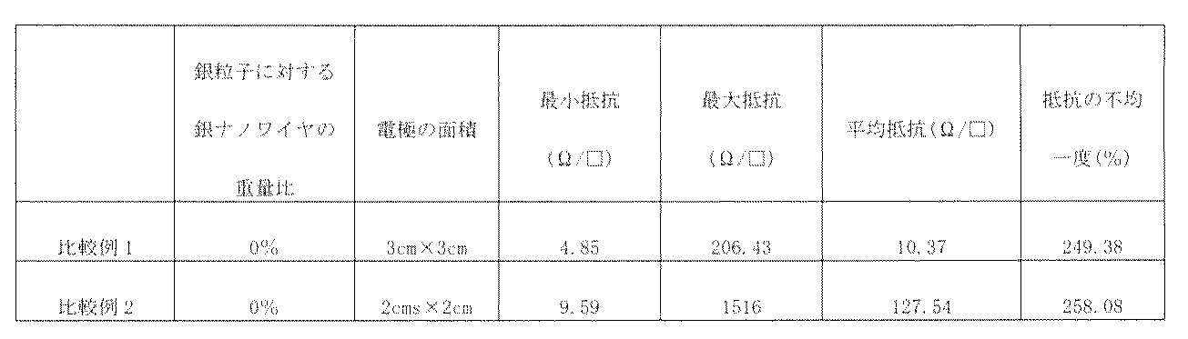
各実施例の導電性複合材料内の銀粒子に対するナノワイヤの重量割合、導電性複合材料を用いて製造された電極の面積、当該電極内に複数のポイントで測定された抵抗の最小値、最大値、平均値、これらの値の不均一度は次の表1の通りである。実施例において、一辺が3cmである試料は100個所で抵抗を測定し、一辺が2cmである試料は49個所で抵抗を測定した。

 〈実施例5~8〉
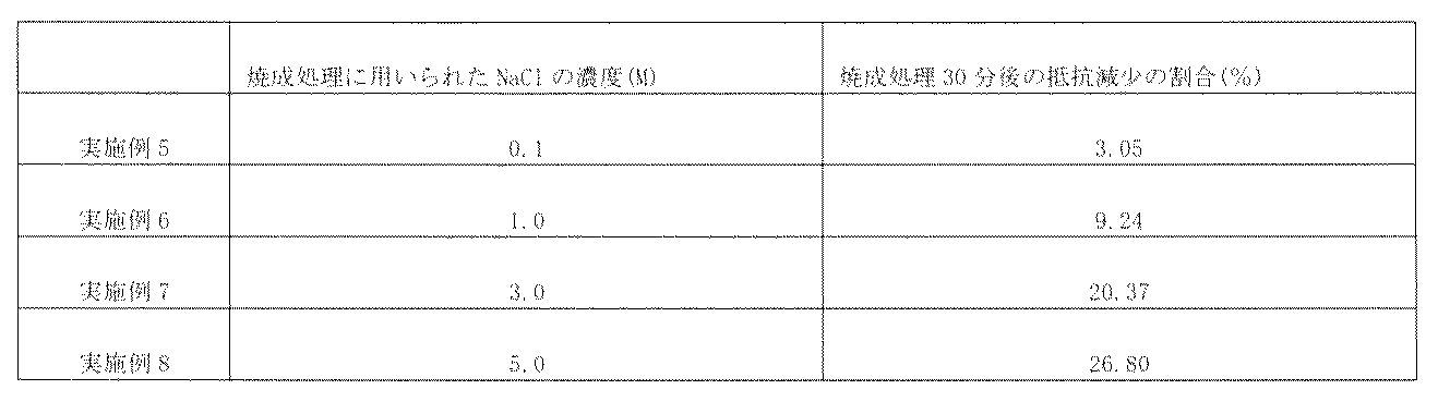
実施例5~8は、実施例1の導電性複合材料で形成された薄膜にNaCl水溶液を用いて化学的な焼成を実施したものである。次の表のように、0.1M~5Mの濃度のNaClで処理し、処理前の抵抗値に対して処理30分後の抵抗値の減少割合を測定した。
〈実施例9及び10〉
実施例9は、実施例1の導電性複合材料を幅が5umであり、深さが3umである凹部が形成されたPET基板に充填して製造されたパターン型電極である。
実施例10は、実施例9のパターン型電極上に20nm厚のITO膜を全体にわたり形成した電極である。
〈比較例1−2〉
比較例1、2は、銀ナノワイヤが混入されないペーストである(株)チャンソンのICP1427だけで製造された薄膜型電極である。
〈実施例1−4と比較例1−2の特性の対比〉
比較例1~2の電極全領域にわたった抵抗の不均一度は約250%であるのに対し、実施例1~4の不均一度は37%~42%で、比較例に比べて1/8に減少したことが分かる。従って、比較例に比べて、実施例1~4は大面積の電極でも全体にわたって均一の抵抗を確保することができる。
〈実施例5−8の特性〉
図2は、実施例1の導電性複合材料で形成された薄膜をさまざまな濃度のNaCl水溶液内に浸漬させて焼成処理した場合、焼成処理時間に応じた抵抗値の変化を測定した結果である。NaCl水溶液の濃度が大きくなるほど抵抗値の減少が大きく、5.0MのNaCl濃度で30分焼成処理をする実施例8の薄膜の場合、抵抗を26.8%だけ減少させることができる。
図3は、実施例8の薄膜の各位置別に抵抗を測定して平均抵抗値と不均一度を測定した結果である。抵抗の不均一度は17.2%と測定され、これは、化学的な焼成処理をしていない実施例1に比べて抵抗の不均一度が約46%減少する。
〈実施例9及び10の特性〉
図4(a)は、実施例9の顕微鏡の写真であり、図4(b)は、電極の凹部の交差する領域を拡大した電子顕微鏡の写真であり、図4(c)は、凹部内の導電性複合材料をより拡大した電子顕微鏡の写真である。これらの写真から確認できるように、凹部内を導電性複合材料が稠密に充填しているので、凹部内の導電性複合材料として形成された電極の形状が均一であり、従って、電極の抵抗も基板全体にわたって一定に維持することができる。
図5は、実施例9および10の光透過特性を測定したもので、実施例9及び10は視光線の全領域で透過率が80%以上であり、特に実施例9は、透過率日90%イサンイムが確認される。
本発明の実施例1~4は、金属ナノ構造体と金属ペーストの混合割合を変化させて製造された導電性複合材料を用いて製造された薄膜型電極である。本実施例の製造に用いられた金属ナノ構造体の分散液は、N&B社の銀ナノワイヤ分散液を用いた。当該分散液の溶媒はイソプロピルアルコールであり、銀ナノワイヤの長さは20umであり、太さは40nmである。本発明の実施例の製造に用いられた銀ペーストは、(株)チャンソンのICP1427であって、含まれた銀粒子は1um、3umの大きさを有し、粘度は約16,200cpsである。これら銀ペーストと銀ナノワイヤ分散液を所定の割合で混合した後、超音波処理をして固形粉が生じずにナノワイヤが均等に分散されるようにした。
各実施例の導電性複合材料内の銀粒子に対するナノワイヤの重量割合、導電性複合材料を用いて製造された電極の面積、当該電極内に複数のポイントで測定された抵抗の最小値、最大値、平均値、これらの値の不均一度は次の表1の通りである。実施例において、一辺が3cmである試料は100個所で抵抗を測定し、一辺が2cmである試料は49個所で抵抗を測定した。
実施例5~8は、実施例1の導電性複合材料で形成された薄膜にNaCl水溶液を用いて化学的な焼成を実施したものである。次の表のように、0.1M~5Mの濃度のNaClで処理し、処理前の抵抗値に対して処理30分後の抵抗値の減少割合を測定した。
実施例9は、実施例1の導電性複合材料を幅が5umであり、深さが3umである凹部が形成されたPET基板に充填して製造されたパターン型電極である。
実施例10は、実施例9のパターン型電極上に20nm厚のITO膜を全体にわたり形成した電極である。
〈比較例1−2〉
比較例1、2は、銀ナノワイヤが混入されないペーストである(株)チャンソンのICP1427だけで製造された薄膜型電極である。
比較例1~2の電極全領域にわたった抵抗の不均一度は約250%であるのに対し、実施例1~4の不均一度は37%~42%で、比較例に比べて1/8に減少したことが分かる。従って、比較例に比べて、実施例1~4は大面積の電極でも全体にわたって均一の抵抗を確保することができる。
〈実施例5−8の特性〉
図2は、実施例1の導電性複合材料で形成された薄膜をさまざまな濃度のNaCl水溶液内に浸漬させて焼成処理した場合、焼成処理時間に応じた抵抗値の変化を測定した結果である。NaCl水溶液の濃度が大きくなるほど抵抗値の減少が大きく、5.0MのNaCl濃度で30分焼成処理をする実施例8の薄膜の場合、抵抗を26.8%だけ減少させることができる。
図3は、実施例8の薄膜の各位置別に抵抗を測定して平均抵抗値と不均一度を測定した結果である。抵抗の不均一度は17.2%と測定され、これは、化学的な焼成処理をしていない実施例1に比べて抵抗の不均一度が約46%減少する。
〈実施例9及び10の特性〉
図4(a)は、実施例9の顕微鏡の写真であり、図4(b)は、電極の凹部の交差する領域を拡大した電子顕微鏡の写真であり、図4(c)は、凹部内の導電性複合材料をより拡大した電子顕微鏡の写真である。これらの写真から確認できるように、凹部内を導電性複合材料が稠密に充填しているので、凹部内の導電性複合材料として形成された電極の形状が均一であり、従って、電極の抵抗も基板全体にわたって一定に維持することができる。
図5は、実施例9および10の光透過特性を測定したもので、実施例9及び10は視光線の全領域で透過率が80%以上であり、特に実施例9は、透過率日90%イサンイムが確認される。
110:基板
120:凹部
130:導電性複合材料
140:ブレード
120:凹部
130:導電性複合材料
140:ブレード
Claims (22)
- 金属ナノ構造体及び金属成分を含み、
上記金属成分は、金属粒子、炭素基盤伝導体及び導電性高分子からなる群より選択されるものである導電性複合材料。 - 第1項において、
前記金属ナノ構造体及び上記金属成分は各々独立して、金、銀、銅、ニッケル、コバルト及びアルミニウムからなる群より選択された少なくとも一つ以上の材料で形成され得る導電性複合材料。 - 第1項において、
前記金属ナノ構造体は、ナノワイヤ構造を有する導電性複合材料。 - 第1項において、
前記金属ナノ構造体の長さは、10μm~50μmである導電性複合材料。 - 第1項において、
上記金属粒子は100nm~10μmである導電性複合材料。 - 第3項において、
前記導電性複合材料に対する前記ナノワイヤ構造を有する金属ナノ構造体の量は0.1~0.5重量%である導電性複合材料。 - 第1項において、
前記炭素基盤伝導体は、導電性カーボンブラック、グラファイト及び炭素ナノチューブからなる群より選択された少なくとも一つを含む導電性複合材料。 - 第1項において、
前記導電性高分子はポリピロール(polypyrrole)、ポリアニリン(polyaniline)、ポルリチオフェン(polythiophene)及びこれらの誘導体からなる群のうち少なくとも一つを含む導電性複合材料。 - 第1項において、
上記金属成分はバインダー、溶剤とともに金属ペーストに含まれたものである導電性複合材料。 - 基板に形成された凹部に第1項~第9項のいずれか一項の導電性複合材料を充填して形成された電極。
- 第10項において、
前記凹部は深さが1~10μmであり、幅が1~10μmである電極。 - 第10項において、
前記基板は透光性を有する電極。 - 第10項において、
上記電極の透光性は90%以上であり、シート抵抗は5Ω/□以下である電極。 - 第10項において、
上記基板は柔軟性を有する電極。 - 第14項の電極及び有機発光層を含む有機発光素子。
- 第15項の発光素子を含む照明器具。
- 基板に形成された凹部に第1項~第9項のいずれか一項の導電性複合材料を充填する段階;及び
前記導電性複合材料を圧着する段階を含む電極の製造方法。 - 第17項において、
前記圧着する段階以後に、前記導電性複合材料に電解質水溶液を印加する化学的な焼成段階をさらに含む電極の製造方法。 - 第18項において、
前記電解質水溶液に含まれた電解物質が、MgCl2、HCl、LiCl、NaCl、MgSO4及びFeSO4からなる群より選択される物質を含む電極の製造方法。 - 第19項において、
前記電解質水溶液は0.1M~5.0M濃度である電極の製造方法。 - 第17項において、
前記圧着する段階以後に80℃~200℃の温度範囲で熱処理を行う段階をさらに含む電極の製造方法。 - 第17項において、
前記基板を洗浄する段階または前記基板を乾燥させる段階をさらに含む電極の製造方法。
Applications Claiming Priority (2)
| Application Number | Priority Date | Filing Date | Title |
|---|---|---|---|
| KR1020150131875A KR20170033725A (ko) | 2015-09-17 | 2015-09-17 | 도전성 복합 재료 및 그 제조 방법 |
| KR10-2015-0131875 | 2015-09-17 |
Publications (1)
| Publication Number | Publication Date |
|---|---|
| WO2017047909A1 true WO2017047909A1 (ja) | 2017-03-23 |
Family
ID=58289009
Family Applications (1)
| Application Number | Title | Priority Date | Filing Date |
|---|---|---|---|
| PCT/KR2016/006297 Ceased WO2017047909A1 (ja) | 2015-09-17 | 2016-06-14 | 導電性複合材料及びその製造方法{conductive composite material and manufacturing method thereof} |
Country Status (2)
| Country | Link |
|---|---|
| KR (1) | KR20170033725A (ja) |
| WO (1) | WO2017047909A1 (ja) |
Cited By (1)
| Publication number | Priority date | Publication date | Assignee | Title |
|---|---|---|---|---|
| CN112331739A (zh) * | 2019-08-05 | 2021-02-05 | 华中科技大学 | 一种低功函导电复合电极、其制备和应用 |
Citations (7)
| Publication number | Priority date | Publication date | Assignee | Title |
|---|---|---|---|---|
| JP2009070660A (ja) * | 2007-09-12 | 2009-04-02 | Kuraray Co Ltd | 透明導電膜およびその製造方法 |
| JP2009094033A (ja) * | 2007-10-12 | 2009-04-30 | Konica Minolta Holdings Inc | 透明導電材料その製造方法及びそれを用いた透明導電素子 |
| JP2009205924A (ja) * | 2008-02-27 | 2009-09-10 | Kuraray Co Ltd | 透明導電膜、透明導電部材、銀ナノワイヤ分散液および透明導電膜の製造方法 |
| JP2010244746A (ja) * | 2009-04-02 | 2010-10-28 | Konica Minolta Holdings Inc | 透明電極、透明電極の製造方法及び有機エレクトロルミネッセンス素子 |
| JP2011108460A (ja) * | 2009-11-16 | 2011-06-02 | Fujifilm Corp | 導電性及び熱伝導性組成物 |
| WO2014185756A1 (ko) * | 2013-05-16 | 2014-11-20 | 주식회사 잉크테크 | 하이브리드 투명전극의 제조방법 및 하이브리드 투명전극 |
| JP2015069908A (ja) * | 2013-09-30 | 2015-04-13 | パナソニック株式会社 | 導電性構造体およびその製造方法 |
-
2015
- 2015-09-17 KR KR1020150131875A patent/KR20170033725A/ko not_active Withdrawn
-
2016
- 2016-06-14 WO PCT/KR2016/006297 patent/WO2017047909A1/ja not_active Ceased
Patent Citations (7)
| Publication number | Priority date | Publication date | Assignee | Title |
|---|---|---|---|---|
| JP2009070660A (ja) * | 2007-09-12 | 2009-04-02 | Kuraray Co Ltd | 透明導電膜およびその製造方法 |
| JP2009094033A (ja) * | 2007-10-12 | 2009-04-30 | Konica Minolta Holdings Inc | 透明導電材料その製造方法及びそれを用いた透明導電素子 |
| JP2009205924A (ja) * | 2008-02-27 | 2009-09-10 | Kuraray Co Ltd | 透明導電膜、透明導電部材、銀ナノワイヤ分散液および透明導電膜の製造方法 |
| JP2010244746A (ja) * | 2009-04-02 | 2010-10-28 | Konica Minolta Holdings Inc | 透明電極、透明電極の製造方法及び有機エレクトロルミネッセンス素子 |
| JP2011108460A (ja) * | 2009-11-16 | 2011-06-02 | Fujifilm Corp | 導電性及び熱伝導性組成物 |
| WO2014185756A1 (ko) * | 2013-05-16 | 2014-11-20 | 주식회사 잉크테크 | 하이브리드 투명전극의 제조방법 및 하이브리드 투명전극 |
| JP2015069908A (ja) * | 2013-09-30 | 2015-04-13 | パナソニック株式会社 | 導電性構造体およびその製造方法 |
Cited By (2)
| Publication number | Priority date | Publication date | Assignee | Title |
|---|---|---|---|---|
| CN112331739A (zh) * | 2019-08-05 | 2021-02-05 | 华中科技大学 | 一种低功函导电复合电极、其制备和应用 |
| CN112331739B (zh) * | 2019-08-05 | 2022-05-20 | 华中科技大学 | 一种低功函导电透明复合电极、其制备和应用 |
Also Published As
| Publication number | Publication date |
|---|---|
| KR20170033725A (ko) | 2017-03-27 |
Similar Documents
| Publication | Publication Date | Title |
|---|---|---|
| US11968787B2 (en) | Metal nanowire networks and transparent conductive material | |
| US12407349B2 (en) | Fused metal nanostructured networks, fusing solutions with reducing agents and methods for forming metal networks | |
| CN104685577B (zh) | 金属纳米结构化网络和透明导电材料 | |
| Yang et al. | Robust and smooth UV-curable layer overcoated AgNW flexible transparent conductor for EMI shielding and film heater | |
| JP5718449B2 (ja) | 金属ナノワイヤを有する透明導体のエッチングパターン形成 | |
| KR101586506B1 (ko) | 충전제 재료를 포함하는 투명한 전도성 코팅 | |
| CN101983181B (zh) | 加热件及其制备方法 | |
| Choi et al. | Uniformly embedded silver nanomesh as highly bendable transparent conducting electrode | |
| JP5569607B2 (ja) | 透明導電膜、透明導電性フィルム及びフレキシブル透明面電極 | |
| KR101872040B1 (ko) | 도전성 고분자 에칭용 잉크 및 도전성 고분자의 패터닝 방법 | |
| CN103408993A (zh) | 导电油墨、透明导电体及其制备方法 | |
| KR101756368B1 (ko) | 유연한 전도성 복합체 필름의 패턴 형성 방법 | |
| CN108028107B (zh) | 功能性细线图案的形成方法及功能性细线图案 | |
| WO2017047909A1 (ja) | 導電性複合材料及びその製造方法{conductive composite material and manufacturing method thereof} | |
| US8921704B2 (en) | Patterned conductive polymer with dielectric patch | |
| KR20160059215A (ko) | 이형상 투명전극 제조방법 | |
| JP5775438B2 (ja) | 銀微粒子分散液 | |
| Jeong et al. | Conductive, flexible transparent electrodes based on mechanically rubbed nonconductive polymer containing silver nanowires | |
| JP6325878B2 (ja) | 平板状銀ナノ粒子の製造方法および平板状銀ナノ粒子含有組成物 | |
| KR20150080370A (ko) | 투명전극용 금속 잉크 및 그 제조방법 | |
| Lü et al. | Preparation of low-resistance and ultra-stable AgNWs@ La2O3-TCF and its application in AC electroluminescence devices | |
| JP5917912B2 (ja) | 銀導電膜およびその製造方法 | |
| CN116052929A (zh) | 一种柔性透明导电薄膜及其制备方法 | |
| CN114171241A (zh) | 一种导电结构及其制备方法、由其制备的电子设备 |
Legal Events
| Date | Code | Title | Description |
|---|---|---|---|
| 121 | Ep: the epo has been informed by wipo that ep was designated in this application |
Ref document number: 16846731 Country of ref document: EP Kind code of ref document: A1 |
|
| NENP | Non-entry into the national phase |
Ref country code: DE |
|
| NENP | Non-entry into the national phase |
Ref country code: JP |
|
| 122 | Ep: pct application non-entry in european phase |
Ref document number: 16846731 Country of ref document: EP Kind code of ref document: A1 |