WO2017047713A1 - 湿式処理による表面粗化方法 - Google Patents
湿式処理による表面粗化方法 Download PDFInfo
- Publication number
- WO2017047713A1 WO2017047713A1 PCT/JP2016/077324 JP2016077324W WO2017047713A1 WO 2017047713 A1 WO2017047713 A1 WO 2017047713A1 JP 2016077324 W JP2016077324 W JP 2016077324W WO 2017047713 A1 WO2017047713 A1 WO 2017047713A1
- Authority
- WO
- WIPO (PCT)
- Prior art keywords
- organic resin
- substrate
- surface roughening
- layer
- roughening method
- Prior art date
- Legal status (The legal status is an assumption and is not a legal conclusion. Google has not performed a legal analysis and makes no representation as to the accuracy of the status listed.)
- Ceased
Links
Images



Classifications
-
- H—ELECTRICITY
- H10—SEMICONDUCTOR DEVICES; ELECTRIC SOLID-STATE DEVICES NOT OTHERWISE PROVIDED FOR
- H10P—GENERIC PROCESSES OR APPARATUS FOR THE MANUFACTURE OR TREATMENT OF DEVICES COVERED BY CLASS H10
- H10P50/00—Etching of wafers, substrates or parts of devices
- H10P50/60—Wet etching
- H10P50/64—Wet etching of semiconductor materials
- H10P50/642—Chemical etching
-
- C—CHEMISTRY; METALLURGY
- C03—GLASS; MINERAL OR SLAG WOOL
- C03C—CHEMICAL COMPOSITION OF GLASSES, GLAZES OR VITREOUS ENAMELS; SURFACE TREATMENT OF GLASS; SURFACE TREATMENT OF FIBRES OR FILAMENTS MADE FROM GLASS, MINERALS OR SLAGS; JOINING GLASS TO GLASS OR OTHER MATERIALS
- C03C15/00—Surface treatment of glass, not in the form of fibres or filaments, by etching
-
- C—CHEMISTRY; METALLURGY
- C03—GLASS; MINERAL OR SLAG WOOL
- C03C—CHEMICAL COMPOSITION OF GLASSES, GLAZES OR VITREOUS ENAMELS; SURFACE TREATMENT OF GLASS; SURFACE TREATMENT OF FIBRES OR FILAMENTS MADE FROM GLASS, MINERALS OR SLAGS; JOINING GLASS TO GLASS OR OTHER MATERIALS
- C03C17/00—Surface treatment of glass, not in the form of fibres or filaments, by coating
- C03C17/006—Surface treatment of glass, not in the form of fibres or filaments, by coating with materials of composite character
- C03C17/008—Surface treatment of glass, not in the form of fibres or filaments, by coating with materials of composite character comprising a mixture of materials covered by two or more of the groups C03C17/02, C03C17/06, C03C17/22 and C03C17/28
- C03C17/009—Mixtures of organic and inorganic materials, e.g. ormosils and ormocers
-
- C—CHEMISTRY; METALLURGY
- C03—GLASS; MINERAL OR SLAG WOOL
- C03C—CHEMICAL COMPOSITION OF GLASSES, GLAZES OR VITREOUS ENAMELS; SURFACE TREATMENT OF GLASS; SURFACE TREATMENT OF FIBRES OR FILAMENTS MADE FROM GLASS, MINERALS OR SLAGS; JOINING GLASS TO GLASS OR OTHER MATERIALS
- C03C17/00—Surface treatment of glass, not in the form of fibres or filaments, by coating
- C03C17/34—Surface treatment of glass, not in the form of fibres or filaments, by coating with at least two coatings having different compositions
-
- C—CHEMISTRY; METALLURGY
- C08—ORGANIC MACROMOLECULAR COMPOUNDS; THEIR PREPARATION OR CHEMICAL WORKING-UP; COMPOSITIONS BASED THEREON
- C08F—MACROMOLECULAR COMPOUNDS OBTAINED BY REACTIONS ONLY INVOLVING CARBON-TO-CARBON UNSATURATED BONDS
- C08F212/00—Copolymers of compounds having one or more unsaturated aliphatic radicals, each having only one carbon-to-carbon double bond, and at least one being terminated by an aromatic carbocyclic ring
- C08F212/02—Monomers containing only one unsaturated aliphatic radical
- C08F212/32—Monomers containing only one unsaturated aliphatic radical containing two or more rings
-
- C—CHEMISTRY; METALLURGY
- C08—ORGANIC MACROMOLECULAR COMPOUNDS; THEIR PREPARATION OR CHEMICAL WORKING-UP; COMPOSITIONS BASED THEREON
- C08G—MACROMOLECULAR COMPOUNDS OBTAINED OTHERWISE THAN BY REACTIONS ONLY INVOLVING UNSATURATED CARBON-TO-CARBON BONDS
- C08G14/00—Condensation polymers of aldehydes or ketones with two or more other monomers covered by at least two of the groups C08G8/00 - C08G12/00
- C08G14/02—Condensation polymers of aldehydes or ketones with two or more other monomers covered by at least two of the groups C08G8/00 - C08G12/00 of aldehydes
- C08G14/04—Condensation polymers of aldehydes or ketones with two or more other monomers covered by at least two of the groups C08G8/00 - C08G12/00 of aldehydes with phenols
- C08G14/06—Condensation polymers of aldehydes or ketones with two or more other monomers covered by at least two of the groups C08G8/00 - C08G12/00 of aldehydes with phenols and monomers containing hydrogen attached to nitrogen
-
- C—CHEMISTRY; METALLURGY
- C09—DYES; PAINTS; POLISHES; NATURAL RESINS; ADHESIVES; COMPOSITIONS NOT OTHERWISE PROVIDED FOR; APPLICATIONS OF MATERIALS NOT OTHERWISE PROVIDED FOR
- C09D—COATING COMPOSITIONS, e.g. PAINTS, VARNISHES OR LACQUERS; FILLING PASTES; CHEMICAL PAINT OR INK REMOVERS; INKS; CORRECTING FLUIDS; WOODSTAINS; PASTES OR SOLIDS FOR COLOURING OR PRINTING; USE OF MATERIALS THEREFOR
- C09D125/00—Coating compositions based on homopolymers or copolymers of compounds having one or more unsaturated aliphatic radicals, each having only one carbon-to-carbon double bond, and at least one being terminated by an aromatic carbocyclic ring; Coating compositions based on derivatives of such polymers
- C09D125/02—Homopolymers or copolymers of hydrocarbons
-
- C—CHEMISTRY; METALLURGY
- C09—DYES; PAINTS; POLISHES; NATURAL RESINS; ADHESIVES; COMPOSITIONS NOT OTHERWISE PROVIDED FOR; APPLICATIONS OF MATERIALS NOT OTHERWISE PROVIDED FOR
- C09D—COATING COMPOSITIONS, e.g. PAINTS, VARNISHES OR LACQUERS; FILLING PASTES; CHEMICAL PAINT OR INK REMOVERS; INKS; CORRECTING FLUIDS; WOODSTAINS; PASTES OR SOLIDS FOR COLOURING OR PRINTING; USE OF MATERIALS THEREFOR
- C09D161/00—Coating compositions based on condensation polymers of aldehydes or ketones; Coating compositions based on derivatives of such polymers
- C09D161/18—Condensation polymers of aldehydes or ketones with aromatic hydrocarbons or their halogen derivatives only
-
- C—CHEMISTRY; METALLURGY
- C09—DYES; PAINTS; POLISHES; NATURAL RESINS; ADHESIVES; COMPOSITIONS NOT OTHERWISE PROVIDED FOR; APPLICATIONS OF MATERIALS NOT OTHERWISE PROVIDED FOR
- C09D—COATING COMPOSITIONS, e.g. PAINTS, VARNISHES OR LACQUERS; FILLING PASTES; CHEMICAL PAINT OR INK REMOVERS; INKS; CORRECTING FLUIDS; WOODSTAINS; PASTES OR SOLIDS FOR COLOURING OR PRINTING; USE OF MATERIALS THEREFOR
- C09D161/00—Coating compositions based on condensation polymers of aldehydes or ketones; Coating compositions based on derivatives of such polymers
- C09D161/34—Condensation polymers of aldehydes or ketones with monomers covered by at least two of the groups C09D161/04, C09D161/18 and C09D161/20
-
- C—CHEMISTRY; METALLURGY
- C09—DYES; PAINTS; POLISHES; NATURAL RESINS; ADHESIVES; COMPOSITIONS NOT OTHERWISE PROVIDED FOR; APPLICATIONS OF MATERIALS NOT OTHERWISE PROVIDED FOR
- C09D—COATING COMPOSITIONS, e.g. PAINTS, VARNISHES OR LACQUERS; FILLING PASTES; CHEMICAL PAINT OR INK REMOVERS; INKS; CORRECTING FLUIDS; WOODSTAINS; PASTES OR SOLIDS FOR COLOURING OR PRINTING; USE OF MATERIALS THEREFOR
- C09D7/00—Features of coating compositions, not provided for in group C09D5/00; Processes for incorporating ingredients in coating compositions
- C09D7/40—Additives
- C09D7/66—Additives characterised by particle size
- C09D7/67—Particle size smaller than 100 nm
-
- C—CHEMISTRY; METALLURGY
- C09—DYES; PAINTS; POLISHES; NATURAL RESINS; ADHESIVES; COMPOSITIONS NOT OTHERWISE PROVIDED FOR; APPLICATIONS OF MATERIALS NOT OTHERWISE PROVIDED FOR
- C09D—COATING COMPOSITIONS, e.g. PAINTS, VARNISHES OR LACQUERS; FILLING PASTES; CHEMICAL PAINT OR INK REMOVERS; INKS; CORRECTING FLUIDS; WOODSTAINS; PASTES OR SOLIDS FOR COLOURING OR PRINTING; USE OF MATERIALS THEREFOR
- C09D7/00—Features of coating compositions, not provided for in group C09D5/00; Processes for incorporating ingredients in coating compositions
- C09D7/40—Additives
- C09D7/66—Additives characterised by particle size
- C09D7/68—Particle size between 100-1000 nm
-
- C—CHEMISTRY; METALLURGY
- C09—DYES; PAINTS; POLISHES; NATURAL RESINS; ADHESIVES; COMPOSITIONS NOT OTHERWISE PROVIDED FOR; APPLICATIONS OF MATERIALS NOT OTHERWISE PROVIDED FOR
- C09K—MATERIALS FOR MISCELLANEOUS APPLICATIONS, NOT PROVIDED FOR ELSEWHERE
- C09K13/00—Etching, surface-brightening or pickling compositions
- C09K13/04—Etching, surface-brightening or pickling compositions containing an inorganic acid
- C09K13/06—Etching, surface-brightening or pickling compositions containing an inorganic acid with organic material
-
- C—CHEMISTRY; METALLURGY
- C09—DYES; PAINTS; POLISHES; NATURAL RESINS; ADHESIVES; COMPOSITIONS NOT OTHERWISE PROVIDED FOR; APPLICATIONS OF MATERIALS NOT OTHERWISE PROVIDED FOR
- C09K—MATERIALS FOR MISCELLANEOUS APPLICATIONS, NOT PROVIDED FOR ELSEWHERE
- C09K13/00—Etching, surface-brightening or pickling compositions
- C09K13/04—Etching, surface-brightening or pickling compositions containing an inorganic acid
- C09K13/08—Etching, surface-brightening or pickling compositions containing an inorganic acid containing a fluorine compound
-
- H—ELECTRICITY
- H10—SEMICONDUCTOR DEVICES; ELECTRIC SOLID-STATE DEVICES NOT OTHERWISE PROVIDED FOR
- H10F—INORGANIC SEMICONDUCTOR DEVICES SENSITIVE TO INFRARED RADIATION, LIGHT, ELECTROMAGNETIC RADIATION OF SHORTER WAVELENGTH OR CORPUSCULAR RADIATION
- H10F19/00—Integrated devices, or assemblies of multiple devices, comprising at least one photovoltaic cell covered by group H10F10/00, e.g. photovoltaic modules
- H10F19/80—Encapsulations or containers for integrated devices, or assemblies of multiple devices, having photovoltaic cells
- H10F19/804—Materials of encapsulations
-
- H—ELECTRICITY
- H10—SEMICONDUCTOR DEVICES; ELECTRIC SOLID-STATE DEVICES NOT OTHERWISE PROVIDED FOR
- H10F—INORGANIC SEMICONDUCTOR DEVICES SENSITIVE TO INFRARED RADIATION, LIGHT, ELECTROMAGNETIC RADIATION OF SHORTER WAVELENGTH OR CORPUSCULAR RADIATION
- H10F71/00—Manufacture or treatment of devices covered by this subclass
-
- H—ELECTRICITY
- H10—SEMICONDUCTOR DEVICES; ELECTRIC SOLID-STATE DEVICES NOT OTHERWISE PROVIDED FOR
- H10F—INORGANIC SEMICONDUCTOR DEVICES SENSITIVE TO INFRARED RADIATION, LIGHT, ELECTROMAGNETIC RADIATION OF SHORTER WAVELENGTH OR CORPUSCULAR RADIATION
- H10F77/00—Constructional details of devices covered by this subclass
- H10F77/70—Surface textures, e.g. pyramid structures
- H10F77/707—Surface textures, e.g. pyramid structures of the substrates or of layers on substrates, e.g. textured ITO layer on a glass substrate
-
- H—ELECTRICITY
- H10—SEMICONDUCTOR DEVICES; ELECTRIC SOLID-STATE DEVICES NOT OTHERWISE PROVIDED FOR
- H10H—INORGANIC LIGHT-EMITTING SEMICONDUCTOR DEVICES HAVING POTENTIAL BARRIERS
- H10H20/00—Individual inorganic light-emitting semiconductor devices having potential barriers, e.g. light-emitting diodes [LED]
- H10H20/01—Manufacture or treatment
-
- H—ELECTRICITY
- H10—SEMICONDUCTOR DEVICES; ELECTRIC SOLID-STATE DEVICES NOT OTHERWISE PROVIDED FOR
- H10H—INORGANIC LIGHT-EMITTING SEMICONDUCTOR DEVICES HAVING POTENTIAL BARRIERS
- H10H20/00—Individual inorganic light-emitting semiconductor devices having potential barriers, e.g. light-emitting diodes [LED]
- H10H20/80—Constructional details
- H10H20/81—Bodies
- H10H20/819—Bodies characterised by their shape, e.g. curved or truncated substrates
- H10H20/82—Roughened surfaces, e.g. at the interface between epitaxial layers
-
- H—ELECTRICITY
- H10—SEMICONDUCTOR DEVICES; ELECTRIC SOLID-STATE DEVICES NOT OTHERWISE PROVIDED FOR
- H10K—ORGANIC ELECTRIC SOLID-STATE DEVICES
- H10K50/00—Organic light-emitting devices
-
- H—ELECTRICITY
- H10—SEMICONDUCTOR DEVICES; ELECTRIC SOLID-STATE DEVICES NOT OTHERWISE PROVIDED FOR
- H10P—GENERIC PROCESSES OR APPARATUS FOR THE MANUFACTURE OR TREATMENT OF DEVICES COVERED BY CLASS H10
- H10P50/00—Etching of wafers, substrates or parts of devices
- H10P50/60—Wet etching
- H10P50/66—Wet etching of conductive or resistive materials
- H10P50/663—Wet etching of conductive or resistive materials by chemical means only
- H10P50/667—Wet etching of conductive or resistive materials by chemical means only by liquid etching only
-
- H—ELECTRICITY
- H10—SEMICONDUCTOR DEVICES; ELECTRIC SOLID-STATE DEVICES NOT OTHERWISE PROVIDED FOR
- H10P—GENERIC PROCESSES OR APPARATUS FOR THE MANUFACTURE OR TREATMENT OF DEVICES COVERED BY CLASS H10
- H10P50/00—Etching of wafers, substrates or parts of devices
- H10P50/69—Etching of wafers, substrates or parts of devices using masks for semiconductor materials
- H10P50/691—Etching of wafers, substrates or parts of devices using masks for semiconductor materials for Group V materials or Group III-V materials
- H10P50/693—Etching of wafers, substrates or parts of devices using masks for semiconductor materials for Group V materials or Group III-V materials characterised by their size, orientation, disposition, behaviour or shape, in horizontal or vertical plane
- H10P50/695—Etching of wafers, substrates or parts of devices using masks for semiconductor materials for Group V materials or Group III-V materials characterised by their size, orientation, disposition, behaviour or shape, in horizontal or vertical plane characterised by the process involved to create the mask, e.g. lift-off masks or sidewalls or to modify the mask
-
- H—ELECTRICITY
- H10—SEMICONDUCTOR DEVICES; ELECTRIC SOLID-STATE DEVICES NOT OTHERWISE PROVIDED FOR
- H10P—GENERIC PROCESSES OR APPARATUS FOR THE MANUFACTURE OR TREATMENT OF DEVICES COVERED BY CLASS H10
- H10P76/00—Manufacture or treatment of masks on semiconductor bodies, e.g. by lithography or photolithography
- H10P76/40—Manufacture or treatment of masks on semiconductor bodies, e.g. by lithography or photolithography of masks comprising inorganic materials
- H10P76/408—Manufacture or treatment of masks on semiconductor bodies, e.g. by lithography or photolithography of masks comprising inorganic materials characterised by their sizes, orientations, dispositions, behaviours or shapes
- H10P76/4085—Manufacture or treatment of masks on semiconductor bodies, e.g. by lithography or photolithography of masks comprising inorganic materials characterised by their sizes, orientations, dispositions, behaviours or shapes characterised by the processes involved to create the masks
-
- C—CHEMISTRY; METALLURGY
- C03—GLASS; MINERAL OR SLAG WOOL
- C03C—CHEMICAL COMPOSITION OF GLASSES, GLAZES OR VITREOUS ENAMELS; SURFACE TREATMENT OF GLASS; SURFACE TREATMENT OF FIBRES OR FILAMENTS MADE FROM GLASS, MINERALS OR SLAGS; JOINING GLASS TO GLASS OR OTHER MATERIALS
- C03C2217/00—Coatings on glass
- C03C2217/40—Coatings comprising at least one inhomogeneous layer
- C03C2217/43—Coatings comprising at least one inhomogeneous layer consisting of a dispersed phase in a continuous phase
- C03C2217/44—Coatings comprising at least one inhomogeneous layer consisting of a dispersed phase in a continuous phase characterized by the composition of the continuous phase
- C03C2217/445—Organic continuous phases
-
- C—CHEMISTRY; METALLURGY
- C03—GLASS; MINERAL OR SLAG WOOL
- C03C—CHEMICAL COMPOSITION OF GLASSES, GLAZES OR VITREOUS ENAMELS; SURFACE TREATMENT OF GLASS; SURFACE TREATMENT OF FIBRES OR FILAMENTS MADE FROM GLASS, MINERALS OR SLAGS; JOINING GLASS TO GLASS OR OTHER MATERIALS
- C03C2217/00—Coatings on glass
- C03C2217/40—Coatings comprising at least one inhomogeneous layer
- C03C2217/43—Coatings comprising at least one inhomogeneous layer consisting of a dispersed phase in a continuous phase
- C03C2217/46—Coatings comprising at least one inhomogeneous layer consisting of a dispersed phase in a continuous phase characterized by the dispersed phase
- C03C2217/47—Coatings comprising at least one inhomogeneous layer consisting of a dispersed phase in a continuous phase characterized by the dispersed phase consisting of a specific material
- C03C2217/475—Inorganic materials
- C03C2217/478—Silica
-
- C—CHEMISTRY; METALLURGY
- C03—GLASS; MINERAL OR SLAG WOOL
- C03C—CHEMICAL COMPOSITION OF GLASSES, GLAZES OR VITREOUS ENAMELS; SURFACE TREATMENT OF GLASS; SURFACE TREATMENT OF FIBRES OR FILAMENTS MADE FROM GLASS, MINERALS OR SLAGS; JOINING GLASS TO GLASS OR OTHER MATERIALS
- C03C2218/00—Methods for coating glass
- C03C2218/30—Aspects of methods for coating glass not covered above
- C03C2218/32—After-treatment
- C03C2218/328—Partly or completely removing a coating
- C03C2218/33—Partly or completely removing a coating by etching
-
- C—CHEMISTRY; METALLURGY
- C08—ORGANIC MACROMOLECULAR COMPOUNDS; THEIR PREPARATION OR CHEMICAL WORKING-UP; COMPOSITIONS BASED THEREON
- C08K—Use of inorganic or non-macromolecular organic substances as compounding ingredients
- C08K3/00—Use of inorganic substances as compounding ingredients
- C08K3/18—Oxygen-containing compounds, e.g. metal carbonyls
- C08K3/20—Oxides; Hydroxides
- C08K3/22—Oxides; Hydroxides of metals
- C08K2003/2237—Oxides; Hydroxides of metals of titanium
- C08K2003/2241—Titanium dioxide
-
- H—ELECTRICITY
- H10—SEMICONDUCTOR DEVICES; ELECTRIC SOLID-STATE DEVICES NOT OTHERWISE PROVIDED FOR
- H10F—INORGANIC SEMICONDUCTOR DEVICES SENSITIVE TO INFRARED RADIATION, LIGHT, ELECTROMAGNETIC RADIATION OF SHORTER WAVELENGTH OR CORPUSCULAR RADIATION
- H10F77/00—Constructional details of devices covered by this subclass
- H10F77/30—Coatings
- H10F77/306—Coatings for devices having potential barriers
- H10F77/311—Coatings for devices having potential barriers for photovoltaic cells
- H10F77/315—Coatings for devices having potential barriers for photovoltaic cells the coatings being antireflective or having enhancing optical properties
-
- H—ELECTRICITY
- H10—SEMICONDUCTOR DEVICES; ELECTRIC SOLID-STATE DEVICES NOT OTHERWISE PROVIDED FOR
- H10K—ORGANIC ELECTRIC SOLID-STATE DEVICES
- H10K2102/00—Constructional details relating to the organic devices covered by this subclass
- H10K2102/301—Details of OLEDs
- H10K2102/331—Nanoparticles used in non-emissive layers, e.g. in packaging layer
-
- Y—GENERAL TAGGING OF NEW TECHNOLOGICAL DEVELOPMENTS; GENERAL TAGGING OF CROSS-SECTIONAL TECHNOLOGIES SPANNING OVER SEVERAL SECTIONS OF THE IPC; TECHNICAL SUBJECTS COVERED BY FORMER USPC CROSS-REFERENCE ART COLLECTIONS [XRACs] AND DIGESTS
- Y02—TECHNOLOGIES OR APPLICATIONS FOR MITIGATION OR ADAPTATION AGAINST CLIMATE CHANGE
- Y02E—REDUCTION OF GREENHOUSE GAS [GHG] EMISSIONS, RELATED TO ENERGY GENERATION, TRANSMISSION OR DISTRIBUTION
- Y02E10/00—Energy generation through renewable energy sources
- Y02E10/50—Photovoltaic [PV] energy
-
- Y—GENERAL TAGGING OF NEW TECHNOLOGICAL DEVELOPMENTS; GENERAL TAGGING OF CROSS-SECTIONAL TECHNOLOGIES SPANNING OVER SEVERAL SECTIONS OF THE IPC; TECHNICAL SUBJECTS COVERED BY FORMER USPC CROSS-REFERENCE ART COLLECTIONS [XRACs] AND DIGESTS
- Y02—TECHNOLOGIES OR APPLICATIONS FOR MITIGATION OR ADAPTATION AGAINST CLIMATE CHANGE
- Y02E—REDUCTION OF GREENHOUSE GAS [GHG] EMISSIONS, RELATED TO ENERGY GENERATION, TRANSMISSION OR DISTRIBUTION
- Y02E10/00—Energy generation through renewable energy sources
- Y02E10/50—Photovoltaic [PV] energy
- Y02E10/549—Organic PV cells
Definitions
- the present invention relates to a surface roughening method on a substrate, and the surface roughening method can be applied to a light extraction layer such as an LED or a low reflection glass of a solar cell.
- the light extraction layer for example, a method of providing a light scattering layer between the light emitting layer inside the organic EL element and the substrate has been proposed (see Patent Document 1, “Particle Dispersion Layer”).
- the light scattering layer is made of a transparent resin in which fine particles having a refractive index different from that of the resin are dispersed.
- the light emitted from the light emitting unit is scattered by the light scattering layer and changes the traveling direction in various directions.
- the multiple scattering light incident within the total reflection angle of the air interface is extracted.
- the size distribution of the fine particles contained therein is preferably wide, the arrangement of the fine particles is preferably random, and the volume fraction of the fine particles is large.
- the size distribution of the fine particles is narrow or the volume fraction of the fine particles is small, the scattering ability of the light scattering layer becomes low, and the purpose cannot be fully achieved.
- the particle size distribution is too wide, it will be difficult to ideally arrange the particles in the resin, and if the particle size distribution is too large when the particle size distribution is wide, the flatness of the light scattering layer Significantly decreases, and the flatness of the light-emitting portion, which is a thin film structure, is impaired, and the reliability of the light-emitting element may be greatly reduced.
- a light extraction layer including a reflection layer and a three-dimensional diffraction layer formed on the reflection layer and including a fine particle having a coefficient of variation of 10% or less and a matrix having a refractive index different from that of the fine particle.
- a layer is disclosed (see Patent Document 2).
- the volume fraction of the fine particles with respect to the volume of the three-dimensional diffraction layer is 50% or more, and the fine particles are arranged in a matrix to form a first region having a short-range periodicity, and The first region is characterized by forming a second region gathered adjacent in a random orientation
- the present invention provides a method for roughening the surface of a substrate. Specifically, by utilizing the difference in wet etching rate between inorganic and organic materials, the surface of the substrate is mixed with inorganic and organic layers, more specifically, the surface of the substrate is etched with inorganic and non-etched organic materials. A roughening layer is formed. Next, the surface of the substrate is exposed by etching the portion where the inorganic substance exists with a solution, and the substrate surface is roughened by etching the substrate, for example, fine irregularities can be formed on the substrate. Various roughening methods are provided.
- the organic resin layer (A) is formed by applying a composition (a3) containing inorganic particles (a1) and an organic resin (a2) on the surface of the substrate, and then drying and curing.
- a first step of forming on the substrate is a step of roughening the surface of the substrate by etching the substrate on which the organic resin layer (A) is formed with a solution containing hydrogen fluoride, hydrogen peroxide, or an acid.
- a surface roughening method comprising two steps.
- the surface roughening method according to the first aspect wherein etching is performed with a solution containing hydrogen fluoride and ammonium salt, hydrogen peroxide and ammonia, hydrogen peroxide and sulfuric acid, or phosphoric acid and nitric acid
- the surface roughening method according to the first aspect wherein etching is performed with a solution containing hydrogen fluoride and ammonium fluoride, or hydrogen peroxide and ammonia
- the surface roughening method according to any one of the first aspect to the third aspect wherein the inorganic particles (a1) are metal oxide particles having an average particle diameter of 5 to 1000 nm
- the composition (a3) is a silica sol in which silica is dispersed in an organic solvent as inorganic particles (a1), or a titanium oxide sol in which titanium oxide is dispersed in an organic solvent as inorganic particles (a1); the surface roughening method according to the first aspect,
- the organic resin (a2) is a resin having a repeating unit structure, and the repeating unit structure repeats a functional group composed of a hydroxy group, a carboxyl group, an amino group, a glycidyl group, or a combination thereof.
- the second step is a step of forming holes having an aspect ratio (height) / (diameter) in the range of 0.1 to 20 in the substrate surface by etching.
- the surface roughening method according to any one of As a ninth aspect, the surface roughening method according to any one of the first to eighth aspects, wherein the organic resin layer (A) is a layer having a layer thickness of 0.001 to 10 ⁇ m,
- the first step before forming the organic resin layer (A), the first step applies a composition (b3) containing the organic resin (b2) on the surface of the substrate, and then performs drying and curing.
- the organic resin (b2) is a resin having a repeating unit structure, and the repeating unit structure repeats a functional group composed of a hydroxy group, a carboxyl group, an amino group, a glycidyl group, or a combination thereof.
- the surface roughening method according to the tenth aspect selected from the organic resin (a2) which is a structure having in the unit structure, As a twelfth aspect, the surface roughening method according to the tenth aspect or the eleventh aspect, wherein the organic resin layer (B) is a layer having a layer thickness of 0.001 to 10 ⁇ m, As a thirteenth aspect, the surface roughening method according to any one of the first to ninth aspects, wherein the composition (a3) further contains a crosslinking agent and a crosslinking catalyst, As a fourteenth aspect, the surface according to any one of the tenth aspect to the twelfth aspect, in which either one or both of the composition (a3) and the composition (b3) further contains a crosslinking agent and a crosslinking catalyst.
- the surface roughening method according to any one of the first aspect to the fourteenth aspect further including a third step of performing gas etching of the substrate surface after the second step A method of using the layer formed by the surface roughening method according to any one of the first aspect to the fifteenth aspect as a light extraction layer of an LED or a low reflection glass layer of a solar cell.
- an ITO electrode, a hole injection layer, a hole transport layer, a light emitting layer, an electron transport layer, an electron injection layer, and an electrode are formed on a substrate such as glass or transparent plastic.
- a substrate such as glass or transparent plastic.
- an N-type semiconductor, a light emitting region, a P-type semiconductor, an ITO electrode, and a SiO 2 layer are formed on a sapphire substrate.
- various light extraction layers for improving the light extraction efficiency have been studied with the aim of improving the light emission efficiency. Furthermore, although the improvement of conversion efficiency is examined in the solar cell, suppressing the sunlight reflection of the surface is mentioned as the leading technique.
- the surface roughening method of the present invention it is possible to roughen the surface of the glass, transparent plastic, SiO 2 layer, etc. used as the light extraction layer, for example, to form fine irregularities. It is possible to reduce the reflection of light, which leads to an improvement in luminous efficiency.
- the surface roughening method of the present invention is also applicable to forming fine irregularities in the reflection reducing layer of the solar cell.
- the present invention differs from those methods in that the substrate surface is physically roughened by etching, for example, unevenness is formed, and the problem of adhesion between the substrate and inorganic particles in the conventional method does not occur.
- a composition (a3) containing inorganic particles (a1) and an organic resin (a2) is applied on the surface of the substrate to be roughened, and then dried and cured to form the organic resin layer (A) on the substrate.
- a first step formed above and a second step for roughening the surface of the substrate by performing etching of the substrate on which the organic resin layer (A) is subsequently formed are included.
- the present invention using the difference in the etching rate of the solution of the inorganic particles (a1) and the organic resin (a2) contained in the organic resin layer (A), at the same time forming irregularities in the organic resin layer (A),
- the organic resin layer (A) (particularly, the organic resin (a2)) functions as a mask in performing solution etching.
- fine irregularities can be easily formed (roughened) on the substrate surface by the formation of the organic resin layer (A) and the subsequent solution etching.
- the roughening of the substrate varies depending on the average particle diameter of the inorganic particles and the concentration (ratio) of the inorganic particles contained in the organic resin layer (A), and is determined by the required roughening shape (uneven shape) on the substrate. be able to.
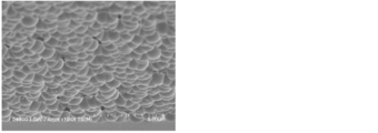
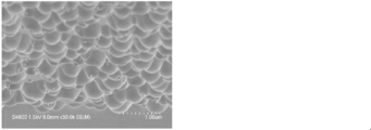
- FIG. 1 is a cross-sectional view of a surface roughening pattern on a SiO 2 film-coated silicon wafer on which a surface roughening forming layer obtained in Example 1 is formed (magnification is 30,000 times, with tilt).
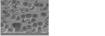
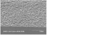
- FIG. 2 is a cross-sectional view of the surface roughening pattern on the SiO 2 film-coated silicon wafer on which the surface roughening forming layer obtained in Example 2 is formed (magnification is 10,000 times, with tilt).
- FIG. 3 is a cross-sectional view of the surface roughening pattern on the SiO 2 film-coated silicon wafer on which the surface roughening forming layer obtained in Example 3 is formed (magnification is 5,000 times, with tilt). .
- FIG. 1 is a cross-sectional view of a surface roughening pattern on a SiO 2 film-coated silicon wafer on which a surface roughening forming layer obtained in Example 1 is formed (magnification is 30,000 times, with tilt).
- FIG. 2 is a cross
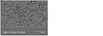
- FIG. 4 is a cross-sectional view of the surface roughening pattern on the SiO 2 film-coated silicon wafer on which the surface roughening forming layer obtained in Example 4 is formed (magnification is 30,000 times, with tilt).
- FIG. 5 is a cross-sectional view of the surface roughening pattern on the SiO 2 film-coated silicon wafer on which the surface roughening forming layer obtained in Example 5 is formed (magnification is 10,000 times, with tilt).
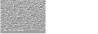
- FIG. 6 is a cross-sectional view of the surface roughening pattern on the SiO 2 film-coated silicon wafer on which the surface roughening forming layer obtained in Example 6 is formed (magnification is 30,000 times, with tilt). .
- FIG. 5 is a cross-sectional view of the surface roughening pattern on the SiO 2 film-coated silicon wafer on which the surface roughening forming layer obtained in Example 5 is formed (magnification is 10,000 times, with tilt).
- FIG. 6 is a cross-sectional view of the surface
- FIG. 7 is a cross-sectional view of the surface roughening pattern on the SiO 2 film-coated silicon wafer on which the surface roughening forming layer obtained in Example 7 is formed (magnification is 30,000 times, with tilt).
- FIG. 8 is a cross-sectional view of the surface roughening pattern on the SiO 2 film-coated silicon wafer on which the surface roughening forming layer obtained in Example 8 was formed (magnification is 30,000 times, with tilt).
- FIG. 9 is a cross-sectional view of a surface roughening pattern on the SiO 2 film-coated silicon wafer on which the surface roughening forming layer obtained in Example 9 is formed (magnification is 30,000 times, with tilt). .
- the present invention relates to a substrate surface roughening method.
- the “roughening” refers to roughening the substrate surface by etching.
- unevenness is formed on the substrate surface by causing a change in the substrate surface by chemical or physical treatment.
- an organic resin layer (A) is formed on a substrate by applying a composition (a3) containing inorganic particles (a1) and an organic resin (a2) on the surface of the substrate, followed by drying and curing. And a second step of roughening the surface of the substrate by etching the substrate on which the organic resin layer (A) is formed with a solution containing hydrogen fluoride, hydrogen peroxide, or an acid. This is a surface roughening method.
- the etching can be preferably performed with a solution containing hydrogen fluoride and ammonium salt, a solution containing hydrogen peroxide and ammonia, a solution containing hydrogen peroxide and sulfuric acid, or a solution containing phosphoric acid and nitric acid.
- a solution containing hydrogen fluoride and an ammonium salt can be used as a buffer solution.
- the etching can be performed with a solution containing hydrogen fluoride and ammonium fluoride, or a solution containing hydrogen peroxide and ammonia.
- etching is performed by wet etching.
- the inorganic particles (a1) in the organic resin layer (A) are etched by the aforementioned solution, while the organic resin (a2) in the organic resin layer (A) exhibits an etching resistance to the solution.
- the substrate can be continuously etched with an acidic aqueous solution.
- the acid used in the acidic aqueous solution include hydrofluoric acid, sulfuric acid, nitric acid, hydrochloric acid, phosphoric acid, and buffered hydrofluoric acid.
- the solution used for etching in the present invention is an aqueous solution, but may further contain an organic solvent.
- the organic solvent is alcohol-based, ether-based, ketone-based, or ester-based. Specific examples thereof include, for example, ethylene glycol monomethyl ether, ethylene glycol monoethyl ether, methyl cellosolve acetate, ethyl cellosolve acetate, propylene glycol monobutyl ether, propylene glycol monobutyl ether acetate, diethylene glycol monomethyl ether, diethylene glycol monoethyl ether, propylene glycol, Propylene glycol monomethyl ether, propylene glycol monomethyl ether acetate, propylene glycol monoethyl ether, propylene glycol monoethyl ether acetate, propylene glycol propyl ether acetate, toluene, xylene, methyl ethyl ketone, cyclopentanone
- the concentration of ammonium salt, acid or ammonia in water or the total solution of water and organic solvent is 0.01 to 97% by mass.
- the concentration is 0.001 to 40% by mass, or 0.01 to 40% by mass.
- an aqueous solution in which NH 4 OH / H 2 O 2 / H 2 O is mixed at a mass ratio of 1: 1: 5 to 0.05: 1: 5 is used.
- a mixed aqueous solution of hydrogen fluoride (acid) and an ammonium fluoride solution it can be used as an aqueous solution in which a 50% by mass hydrofluoric acid aqueous solution and a 40% by mass ammonium fluoride aqueous solution are mixed.
- a metal oxide is used as the inorganic particles (a1) used in the present invention.
- examples thereof include silicon oxide (silica), titanium oxide, zirconium oxide, aluminum oxide, silicon nitride, and titanium nitride.
- silicon oxide (silica) is preferable.
- the average particle diameter can be 5 to 1000 nm, 5 to 200 nm, or 10 to 50 nm.
- These inorganic particles are preferably added to the organic resin (a2) in a colloidal state, that is, the sol dispersed in the organic solvent of the inorganic particles (a1) is added to the organic resin (a2) or the organic resin (a2) solution.
- a composition (a3) is obtained by adding. This composition (a3) is used for coating a substrate as described later.
- a silica sol in which silica is dispersed in an organic solvent or a titanium oxide sol in which titanium oxide is dispersed in an organic solvent is used as the inorganic particles (a1), and these sols and a solution of the organic resin (a2) are mixed.
- a composition (a3) is obtained.
- the average particle diameter of the fine particles is a value obtained by observing the fine particles in the sol with an electron microscope.
- the organic resin layer (A) obtained by applying the composition (a3) and the composition (a3) and then drying and curing the inorganic particles (a1) and the organic resin (a2) with the organic resin (A2)
- the inorganic particles (a1) are contained in an amount of 1 to 100 parts by mass or 5 to 70 parts by mass with respect to 100 parts by mass.
- the organic resin (a2) is a resin having a repeating unit structure, in which the repeating unit structure has a polar group composed of a hydroxy group, a carboxyl group, an amino group, a glycidyl group, or a combination thereof as a functional group. It is preferable that These functional groups are preferable in terms of compatibility with inorganic particles and coatability on a substrate. Moreover, these functional groups are preferable also in the point that a cured film becomes insoluble with respect to acidic aqueous solution. Examples of the resin containing the functional group include acrylic resins and novolac resins. Further, as the organic resin (a2), polyether, polyether ether ketone material, and epoxy resin can be used.
- acrylic resin examples include homopolymers of monomers having a hydroxy group, a carboxyl group, an amino group, or a glycidyl group, and copolymers of these with monomers constituting other resins.
- monomer examples include (meth) acrylic acid, (meth) acrylic acid ester, and vinyl compounds.
- Monomers having a hydroxy group, carboxyl group, amino group, or glycidyl group include (meth) acrylic acid, (meth) acrylamide, hydroxyalkyl (meth) acrylate, carboxyalkyl (meth) acrylate, aminoalkyl (meth) acrylate, and glycidyl.
- Monomers such as (meth) acrylate, hydroxystyrene, hydroxyvinylnaphthalene, vinyl benzoate and the like can be mentioned.
- examples of monomers constituting other resins include monomers not containing the above functional groups.
- alkyl (meth) acrylates such as methyl (meth) acrylate and ethyl (meth) acrylate, phenyl (meth) acrylate, benzyl ( And (meth) acrylate, styrene, t-butylstyrene, vinylnaphthalene and the like.
- the above acrylic resins can be obtained by radical polymerization or cationic polymerization of these acrylic monomers.
- polyether and polyether ether ketone materials examples include polyethers and polyether ether ketones obtained by a reaction between a phenolic hydroxy group-containing compound and a halogen group-containing aromatic compound.
- the novolac resin includes a novolac resin obtained by reaction of a phenolic hydroxy group-containing compound or amino group-containing aromatic compound and an aldehyde compound, a phenolic hydroxy group-containing compound or amino group-containing aromatic compound, and a hydroxy group. And a novolak resin obtained by a reaction with an aldehyde compound containing carboxyl group or amino group.
- Examples of the compound having a phenolic hydroxy group include monohydric phenols such as phenol, cresol, salicylic acid and naphthol, dihydric phenols such as catechol and resorcinol, trihydric phenols such as pyrogallol and phloroglicinol, biphenol, bisphenol A, and bisphenol S. And polynuclear phenols.
- Examples of the amino group-containing aromatic compound include pyrrole, phenylnaphthylamine, phenylindole, carbazole, diphenylamine, and 3-hydroxydiphenylamine.
- Aldehydes include formaldehyde, paraformaldehyde, acetaldehyde, propylaldehyde, butyraldehyde, isobutyraldehyde, valeraldehyde, capronaldehyde, 2-methylbutyraldehyde, 2-ethylhexylaldehyde (2-ethylhexanal), hexylaldehyde, undecane aldehyde, 7 -Saturated fats such as methoxy-3,7-dimethyloctylaldehyde, cyclohexanealdehyde, cyclohexane carbaldehyde, 3-methyl-2-butyraldehyde, glyoxal, malonaldehyde, malondialdehyde, succinaldehyde, glutaraldehyde, adipine aldehyde Aldehydes, unsaturated alipha
- hydroxy group or carboxyl group-containing aldehyde compounds are preferable, and examples thereof include hydroxybenzaldehyde, carboxybenzaldehyde, hydroxynaphthaldehyde, carboxynaphthaldehyde, hydroxypyrenealdehyde, and carboxypyrenealdehyde.
- the phenolic hydroxy group-containing compound, amino group-containing aromatic compound and aldehyde compound can use aldehydes in a ratio of 0.1 to 10 equivalents per 1 equivalent of the phenyl group.
- Examples of the acid catalyst used in the condensation reaction include mineral acids such as sulfuric acid, phosphoric acid, and perchloric acid, and organic sulfonic acids such as trifluoromethanesulfonic acid, p-toluenesulfonic acid, and p-toluenesulfonic acid monohydrate. Carboxylic acids such as formic acid and oxalic acid are used.
- the amount of the acid catalyst used is variously selected depending on the type of acids used. Usually, the acid catalyst is used in an amount of 0.001 to 10,000 parts by mass, preferably 0.001 parts by mass with respect to 100 parts by mass of the total of the phenolic hydroxy group-containing compound or amino group-containing aromatic compound and aldehyde compound. The amount is from 01 to 1,000 parts by mass, more preferably from 0.1 to 100 parts by mass.
- the above condensation reaction is carried out without a solvent, but is usually carried out using a solvent. Any solvent that does not inhibit the reaction can be used. Examples thereof include ethers such as butyl cellosolve (2-butoxyethanol) and cyclic ethers such as tetrahydrofuran and dioxane. Further, if the acid catalyst used is a liquid such as formic acid, the acid catalyst can also serve as a solvent.
- the reaction temperature during the condensation is usually 40 ° C to 200 ° C.
- the reaction time is variously selected depending on the reaction temperature, but is usually about 30 minutes to 50 hours.
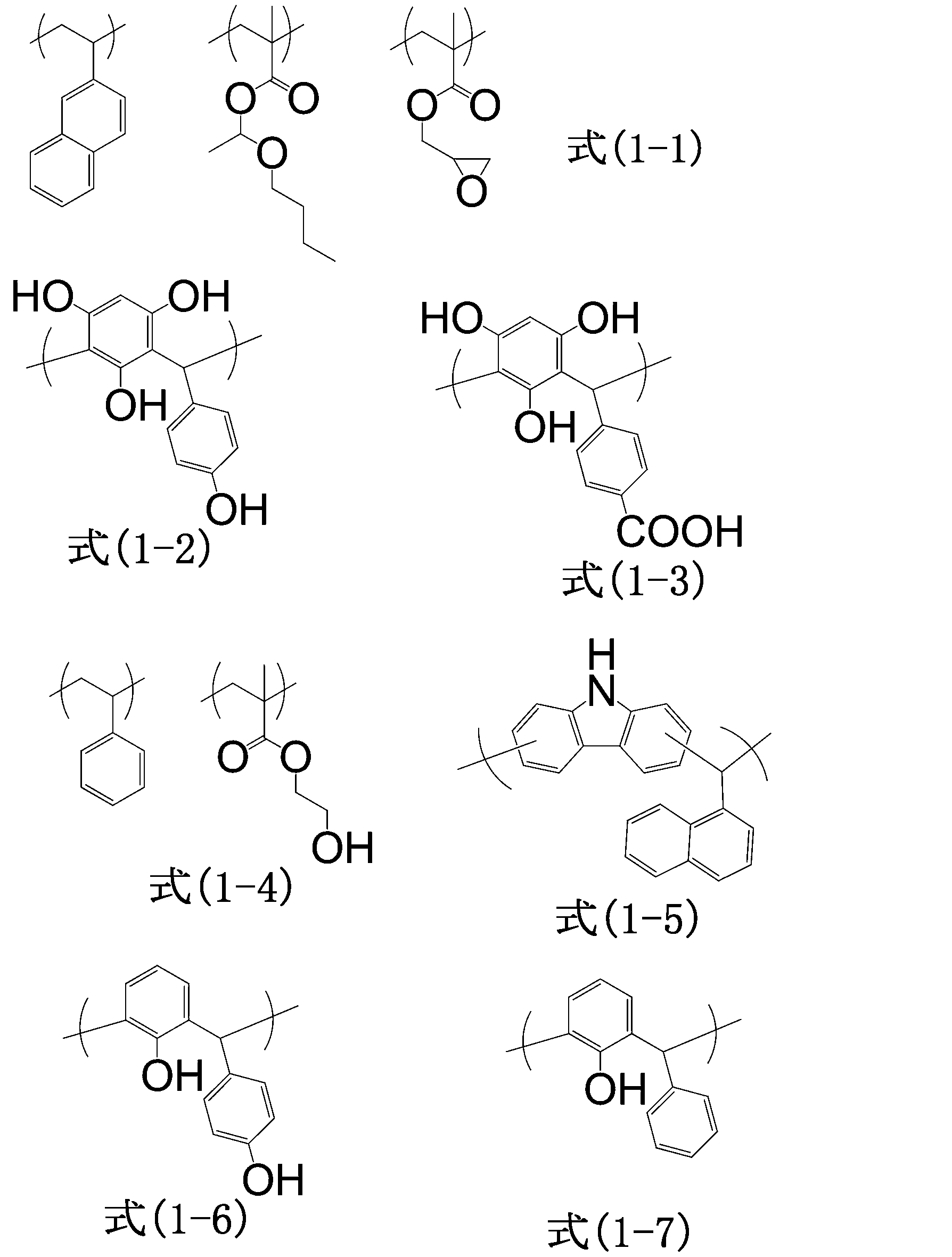
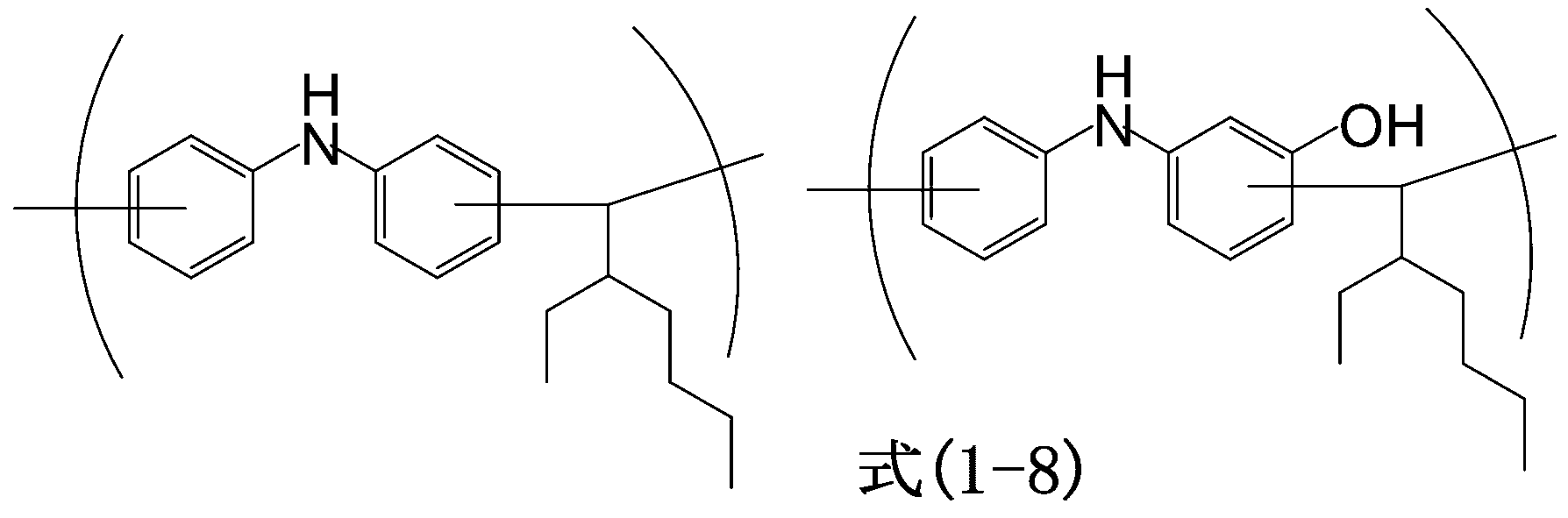
- Examples of the organic resin (a2) used in the present invention include resins having a repeating unit structure represented by the following formulas (1-1) to (1-8).
- an epoxy resin can be used in addition to the above-mentioned acrylic resin and novolac resin.
- the epoxy resin include polyfunctional epoxy compounds such as butanetetracarboxylic acid tetra (3,4-epoxycyclohexylmethyl) modified ⁇ -caprolactone (manufactured by Daicel Corporation, trade name: Epolide GT401, alicyclic epoxy). Can be used.
- the organic resin (a2) used in the present invention has a weight average molecular weight (Mw) in terms of polystyrene of gel permeation chromatography (GPC) of 600 to 1,000,000, or 600 to 200,000.
- Mw weight average molecular weight in terms of polystyrene of gel permeation chromatography
- the composition (a3) used for this invention contains the said organic resin (a2), inorganic particle (a1), and a solvent. If necessary, additives such as surfactants described later can be included.
- the solid content may be 0.1 to 70% by mass, or 0.1 to 60% by mass with respect to the total mass of the composition (a3). Solid content means the remaining component remove
- the organic resin (a2) can be used in a proportion of 1 to 99.9% by mass, or 20 to 99.9% by mass with respect to the total mass of the solid content.
- the surface roughening method of the present invention includes: 1st process)
- the organic resin layer (A) is apply
- Forming, and 2nd process) The process of roughening the surface of this board
- a step of performing gas etching of the substrate surface may be included. That is, in the present invention, after the organic resin layer (A) is formed on the substrate, etching (wet etching or wet etching and gas etching) is performed from above the substrate to roughen the surface of the substrate.
- the first step is to apply the composition (b3) containing the organic resin (b2) on the surface of the substrate before forming the organic resin layer (A), and then A first ′ step of forming the organic resin layer (B) on the substrate by drying and curing may be further included.
- the organic resin layer (B) is formed on the substrate, the organic resin layer (A) is formed on the organic resin layer (B), and then the substrate is etched (wet etching or wet etching and gas Etching) to roughen the surface of the substrate.
- the organic resin (b2) contained in the organic resin layer (B) is a resin in the same range as the organic resin (a2) of the organic resin layer (A):
- the repeating unit structure is selected from the organic resin (a2) having a repeating unit structure having a functional group composed of a hydroxy group, a carboxyl group, an amino group, a glycidyl group, or a combination thereof. can do.
- the same resin can be used for the organic resin (b2) and the organic resin (a2).
- the composition (b3) used in the present invention contains the organic resin (b2) and a solvent. If necessary, additives such as surfactants described later can be included.
- the solid content may be 0.1 to 70% by mass, or 0.1 to 60% by mass with respect to the total mass of the composition (b3). Solid content means the remaining component remove
- the organic resin (b2) can be used in a proportion of 1 to 100% by mass, or 1 to 99.9% by mass, or 50 to 99.9% by mass with respect to the total mass of the solid content.
- the organic resin (b2) used in the present invention has a weight average molecular weight (Mw) in terms of polystyrene of gel permeation chromatography (GPC) of 600 to 1,000,000, or 600 to 200,000.
- the organic resin layer (B) is obtained by applying the composition (b3) on a substrate, then drying and curing, and the organic resin layer (A) is formed on the organic resin layer (B). Since (a3) is overcoated, in order to prevent intermixing (layer mixing), the composition (b3) can further contain a crosslinking agent and a crosslinking catalyst. Moreover, a crosslinking agent and a crosslinking catalyst can be contained also in the composition (a3) which forms an organic resin layer (A) if necessary.
- crosslinking agent used in the composition (a3) and the composition (b3) examples include melamine-based, substituted urea-based, or their polymer-based materials.
- a cross-linking agent having at least two cross-linking substituents methoxymethylated glycoluril, butoxymethylated glycoluril, methoxymethylated melamine, butoxymethylated melamine, methoxymethylated benzogwanamine, butoxymethylated benzogwanamine, Compounds such as methoxymethylated urea, butoxymethylated urea, methoxymethylated thiourea, or methoxymethylated thiourea.
- the condensate of these compounds can also be used.
- the addition amount of the crosslinking agent varies depending on the coating solvent to be used, the base substrate to be used, the required solution viscosity, the required film shape, etc., but the total solid content of the composition (a3) or the composition (b3) It is 0.001 to 80% by mass, preferably 0.01 to 50% by mass, and more preferably 0.05 to 40% by mass with respect to the total mass.
- a catalyst for promoting the crosslinking reaction
- p-toluenesulfonic acid trifluoromethanesulfonic acid
- pyridinium p-toluenesulfonic acid pyridinium p-toluenesulfonic acid
- salicylic acid sulfosalicylic acid
- citric acid benzoic acid
- hydroxybenzoic acid Contains acidic compounds such as naphthalenecarboxylic acid or / and thermal acid generators such as 2,4,4,6-tetrabromocyclohexadienone, benzoin tosylate, 2-nitrobenzyl tosylate, and other organic sulfonic acid alkyl esters I can do it.
- the blending amount of the crosslinking catalyst is 0.0001 to 20% by mass, preferably 0.0005 to 10% by mass, preferably 0.005% by mass with respect to the total mass of the total solid content of the composition (a3) or the composition (b3). 01 to 3% by mass.
- examples of the surfactant that can be used in the composition (a3) or the composition (b3) include polyoxyethylene lauryl ether, polyoxyethylene stearyl ether, polyoxyethylene cetyl ether, polyoxyethylene oleyl ether, and the like.
- Polyoxyethylene alkyl ethers polyoxyethylene octylphenol ether, polyoxyethylene alkyl allyl ethers such as polyoxyethylene nonylphenol ether, polyoxyethylene / polyoxypropylene block copolymers, sorbitan monolaurate, sorbitan monopalmitate, Sorbitan monostearate, sorbitan monooleate, sorbitan trioleate, sorbitan fatty acid esters such as sorbitan tristearate, polio Nonionic series such as polyoxyethylene sorbitan fatty acid esters such as ciethylene sorbitan monolaurate, polyoxyethylene sorbitan monopalmitate, polyoxyethylene sorbitan monostearate, polyoxyethylene sorbitan trioleate, polyoxyethylene sorbitan tristearate Surfactant, F-top EF301, EF303, EF352 (trade name, manufactured by Tokem Products Co., Ltd.
- the compounding amount of these surfactants is usually 2.0% by mass or less, preferably 1.0% by mass or less, based on the total mass of the total solid content of the composition (a3) or the composition (b3). .
- These surfactants may be added alone or in combination of two or more.
- the solvent that can be used in the composition (a3) or the composition (b3) is ethylene glycol monomethyl ether, ethylene glycol monoethyl ether, methyl cellosolve acetate, ethyl cellosolve acetate, diethylene glycol monomethyl ether, diethylene glycol monoethyl ether.
- organic solvents are used alone or in combination of two or more.
- high boiling point solvents such as propylene glycol monobutyl ether and propylene glycol monobutyl ether acetate can be mixed and used.
- propylene glycol monomethyl ether, propylene glycol monomethyl ether acetate, ethyl lactate, butyl lactate, cyclohexanone and the like are preferable for improving the leveling property.
- the composition (a3) is applied onto the surface of the substrate or base material by an appropriate application method using a spinner, coater, etc., then baked (dried) and cured to form the organic resin layer (A) on the substrate. Created above (first step).
- the composition (b3) is first applied on the surface of the substrate or base material by an appropriate application method using a spinner, coater, etc., and then baked (dried).
- the organic resin layer (A) may be formed on the organic resin layer (B) by the above-described procedure.
- the organic resin layer (A) is preferably a layer having a layer thickness of 0.001 to 10 ⁇ m, or 0.005 to 3.0 ⁇ m.
- the organic resin layer (B) is preferably a layer having a layer thickness of 0.001 to 10 ⁇ m or 0.005 to 3.0 ⁇ m.
- the organic resin layer (A) is a layer that contributes to roughening the surface of the substrate by etching, which will be described later, and is also referred to as a “surface roughening layer” in this specification.
- the conditions for baking after applying the composition (a3) or (b3) are 80 to 400 ° C. and 0.5 to 120 minutes.
- the substrate on which the organic resin layer (A) is formed is described in detail from above the substrate.
- the surface of the substrate is roughened by etching with the solution (second step). By this wet etching, only the portion where the inorganic particles (a1) are present in the organic resin layer (A) is scraped off in the vertical direction. When the etching reaches the surface of the substrate, it is also possible to continue etching with the solution, thereby forming irregularities on the substrate and roughening the surface.
- the substrate includes not only the substrate itself but also a coated substrate obtained by coating SiO 2 or the like on the substrate, and the surface of the substrate or the surface of the coated substrate can be roughened by the method of the present invention.
- Etching with the above solution (second step) is performed until a hole having an aspect ratio (height) / (diameter) of 0.1 to 20 or 0.1 to 10 is formed on the substrate surface by etching. Done.
- the etching time is about 1 second to 1 hour, or about 5 seconds to 10 minutes.
- the substrate include silicon, silicon oxide, glass, and sapphire.
- the organic resin layer (B) is formed on the substrate by coating, and then the organic resin layer (A) is formed thereon, and the organic resin layer (A) is first wet-etched using the above solution. Thereafter, the organic resin layer (B) can be gas-etched to process the substrate.
- tetrafluoromethane CF 4
- perfluorocyclobutane C 4 F 8
- perfluoropropane C 3 F 8
- trifluoromethane CHF 3
- difluoromethane CH 2 F 2
- Gases such as carbon monoxide, argon, oxygen, nitrogen, sulfur hexafluoride, nitrogen trifluoride and chlorine trifluoride, chlorine, trichloroborane and dichloroborane can be used.
- the layer formed by the surface roughening method of the present invention can be suitably used as an LED light extraction layer or a low reflection glass layer of a solar cell.
- the reaction solution was cooled and then poured into methanol, and the polymer was reprecipitated and dried by heating to obtain a polymer having a repeating unit structure represented by the formula (1-1).
- the weight average molecular weight Mw of the obtained polymer was 6,000 (polystyrene conversion).
- the ratio of the repeating unit structure (number) formed from 2-vinylnaphthalene is 0.8, and glycidyl methacrylate
- the ratio of the repeating unit structure (number) formed from 0.1 was 0.1, and the ratio of the repeating unit structure (number) formed from 1-butoxyethyl methacrylate was 0.1.
- composition (a3) As an organic resin (a2), 0.3 g of a trade name Epolide GT401 (manufactured by Daicel Chemical Co., Ltd.), an organosilica sol solution (manufactured by Nissan Chemical Industries, Ltd., trade name MIBK-ST, a dispersion medium is methyl isobutyl ketone, and a silica concentration is 30). (Mass%, average particle size is 10 to 15 nm) 0.5 g, 48.78 g of propylene glycol monomethyl ether acetate, and 0.1 g of propylene glycol monomethyl ether to obtain a solution. Thereafter, the solution was filtered using a polyethylene microfilter having a pore diameter of 0.2 ⁇ m to prepare a solution of the composition (a3-8).
- Epolide GT401 manufactured by Daicel Chemical Co., Ltd.
- an organosilica sol solution manufactured by Nissan Chemical Industries, Ltd., trade name MIBK-ST, a dispersion medium is methyl is
- Example 1 The solution of the composition (a3-1) obtained in Surface Roughening Material Preparation Example 1 was applied to a TEOS substrate (SiO 2 film-coated silicon wafer) with a spin coater, and baked at 240 ° C. for 1 minute, and a 15 nm organic resin layer A (surface roughening forming layer) was formed.
- Example 2 The solution of the composition (a3-2) obtained in Surface Roughening Material Preparation Example 2 was applied to a TEOS substrate (SiO 2 film-coated silicon wafer) with a spin coater, and baked at 240 ° C. for 1 minute to obtain a 40 nm organic resin layer. A (surface roughening forming layer) was formed.
- Example 3 The solution of the composition (a3-3) obtained in Surface Roughening Material Preparation Example 3 was applied to a TEOS substrate (SiO 2 film-coated silicon wafer) with a spin coater, and baked at 240 ° C. for 1 minute, and a 90 nm organic resin layer A (surface roughening forming layer) was formed.
- Example 4 A solution of the composition (a3-4) obtained in Surface Roughening Material Preparation Example 4 was applied to a TEOS substrate (SiO 2 film-coated silicon wafer) with a spin coater, and baked at 240 ° C. for 1 minute to form a 15 nm organic resin layer. A (surface roughening forming layer) was formed.
- Example 5 A solution of the composition (a3-5) obtained in Surface Roughening Material Preparation Example 5 was applied to a TEOS substrate (SiO 2 film-coated silicon wafer) with a spin coater, and baked at 240 ° C. for 1 minute to obtain a 40 nm organic resin layer. A (surface roughening forming layer) was formed.
- Example 6 A solution of the composition (a3-6) obtained in Surface Roughening Material Preparation Example 6 was applied to a TEOS substrate (SiO 2 film-coated silicon wafer) with a spin coater, and baked at 240 ° C. for 1 minute to obtain a 40 nm organic resin layer. A (surface roughening forming layer) was formed.
- Example 7 A solution of the composition (a3-7) obtained in Surface Roughening Material Preparation Example 7 was applied to a TEOS substrate (SiO 2 film-coated silicon wafer) with a spin coater, and baked at 240 ° C. for 1 minute to form a 15 nm organic resin layer. A (surface roughening forming layer) was formed.
- Example 8 A solution of the composition (a3-5) obtained in Surface Roughening Material Preparation Example 5 was applied to a TEOS substrate (SiO 2 film-coated silicon wafer) with a spin coater, and baked at 240 ° C. for 1 minute to obtain a 40 nm organic resin layer. A (surface roughening forming layer) was formed.
- Example 9 A solution of the composition (a3-8) obtained in Surface Roughening Material Preparation Example 8 was applied to a TEOS substrate (SiO 2 film-coated silicon wafer) with a spin coater, baked at 240 ° C. for 1 minute, and a 15 nm organic resin layer A (surface roughening forming layer) was formed.
- Example 10 A solution of the composition (a3-9) obtained in Surface Roughening Material Preparation Example 9 was applied to a TiN substrate with a spin coater and baked at 300 ° C. for 1 minute, and a 15 nm organic resin layer A (surface roughening layer) Formed.
- Comparative Example 1 The solution of the comparative composition (a3-10) obtained in Comparative Preparation Example 1 was applied to a TEOS substrate (SiO 2 film-coated silicon wafer) with a spin coater, baked at 240 ° C. for 1 minute, and a 40 nm organic resin layer A ( Surface roughening layer) was formed.
- a TEOS substrate SiO 2 film-coated silicon wafer
- a spin coater baked at 240 ° C. for 1 minute
- a 40 nm organic resin layer A Surface roughening layer
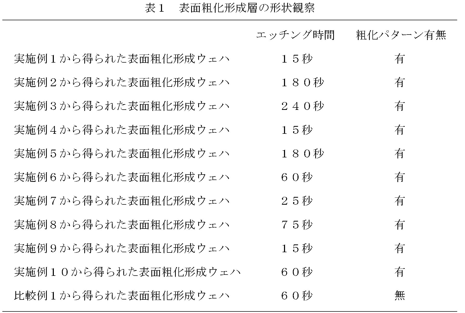
- Etching / ashing removal was performed on the wafer on which the surface roughening layer formed from Examples 1 to 9 was formed, and the surface of the wafer with the roughened surface was scanned using a scanning electron microscope (Hitachi S-4800). The surface roughening pattern shape was observed (see FIGS. 1 to 9).
- the present invention provides a method for roughening the surface of a substrate. Specifically, by utilizing the etching rate difference between the inorganic and organic solutions, a layer containing both inorganic and organic materials on the substrate, more specifically, a portion etched by the solution and a portion not etched on the surface of the substrate are mixed. A surface roughening layer to be formed is formed. Next, the surface of the substrate is exposed by etching the portion where the inorganic substance exists with the solution, and at the same time, the surface of the SiO 2 coated substrate is also roughened by etching the solution, thereby forming, for example, fine irregularities on the substrate. Can do. Utilizing these, the surface roughening method of the present invention can be applied to the formation of light extraction layers such as LEDs and low reflection layers of solar cells.
Landscapes
- Chemical & Material Sciences (AREA)
- Organic Chemistry (AREA)
- Engineering & Computer Science (AREA)
- Materials Engineering (AREA)
- Life Sciences & Earth Sciences (AREA)
- Chemical Kinetics & Catalysis (AREA)
- General Chemical & Material Sciences (AREA)
- Wood Science & Technology (AREA)
- Geochemistry & Mineralogy (AREA)
- Inorganic Chemistry (AREA)
- Medicinal Chemistry (AREA)
- Health & Medical Sciences (AREA)
- Polymers & Plastics (AREA)
- Nanotechnology (AREA)
- Composite Materials (AREA)
- Optics & Photonics (AREA)
- Physics & Mathematics (AREA)
- Electroluminescent Light Sources (AREA)
- Photovoltaic Devices (AREA)
- Treatments Of Macromolecular Shaped Articles (AREA)
- Weting (AREA)
- Led Devices (AREA)
- Materials For Photolithography (AREA)
- Laminated Bodies (AREA)
- Printing Plates And Materials Therefor (AREA)
Abstract
Description
第2観点として、エッチングがフッ化水素とアンモニウム塩、過酸化水素とアンモニア、過酸化水素と硫酸、又はリン酸と硝酸を含む溶液で行われる、第1観点に記載の表面粗化方法、
第3観点として、エッチングがフッ化水素とフッ化アンモニウム、又は過酸化水素とアンモニアを含む溶液で行われる、第1観点に記載の表面粗化方法、
第4観点として、無機粒子(a1)が平均粒子径5~1000nmの金属酸化物粒子である第1観点乃至第3観点、のいずれか一つに記載の表面粗化方法、
第5観点として、組成物(a3)が、無機粒子(a1)としてシリカが有機溶剤に分散したシリカゾル、又は無機粒子(a1)として酸化チタニウムが有機溶剤に分散した酸化チタニウムゾルと、有機樹脂(a2)の溶液との混合物である、第1観点に記載の表面粗化方法、
第6観点として、有機樹脂層(A)が、無機粒子(a1)及び有機樹脂(a2)を、有機樹脂(a2)100質量部に対して無機粒子(a1)5~70質量部の割合で含有する、第1観点乃至第5観点のいずれか一つに記載の表面粗化方法、
第7観点として、有機樹脂(a2)が、繰り返し単位構造を有する樹脂であって、該繰り返し単位構造は、ヒドロキシ基、カルボキシル基、アミノ基、グリシジル基、又はそれらの組み合わせからなる官能基を繰り返し単位構造内に有する構造からなる、第1観点乃至第6観点のいずれか一つに記載の表面粗化方法、
第8観点として、第2工程が、エッチングにより基板表面にアスペクト比(高さ)/(直径)で0.1~20の範囲にある孔を形成する工程である、第1観点乃至第7観点のいずれか一つに記載の表面粗化方法、
第9観点として、有機樹脂層(A)が0.001~10μmの層厚を有する層である、第1観点乃至第8観点のいずれか一つに記載の表面粗化方法、
第10観点として、第1工程が、有機樹脂層(A)を形成する前に、基板の表面上に有機樹脂(b2)を含む組成物(b3)を塗布し、次いで乾燥と硬化を為すことにより有機樹脂層(B)を該基板上に形成する第1’工程を更に含む、第1観点乃至第9観点のいずれか一つに記載の表面粗化方法、
第11観点として、有機樹脂(b2)が、繰り返し単位構造を有する樹脂であって、該繰り返し単位構造は、ヒドロキシ基、カルボキシル基、アミノ基、グリシジル基、又はそれらの組み合わせからなる官能基を繰り返し単位構造内に有する構造である有機樹脂(a2)から選択される、第10観点に記載の表面粗化方法、
第12観点として、有機樹脂層(B)が0.001~10μmの層厚を有する層である、第10観点又は第11観点に記載の表面粗化方法、
第13観点として、組成物(a3)が更に架橋剤と架橋触媒を含有してする、第1観点乃至第9観点のいずれか一つに記載の表面粗化方法、
第14観点として、組成物(a3)及び組成物(b3)の何れか一方もしくは双方が、更に架橋剤と架橋触媒を含有する、第10観点乃至第12観点のいずれか1項に記載の表面粗化方法、
第15観点として、第2工程の後に、基板表面のガスエッチングを為す第3工程を更に含む、第1観点乃至第14観点のいずれか一つに記載の表面粗化方法、及び
第16観点として、第1観点乃至第15観点のいずれか1項に記載の表面粗化方法により形成された層を、LEDの光取り出し層、又は太陽電池の低反射ガラス層として使用する方法、である。
またLEDでは、サファイア基板上にN型半導体、発光域、P型半導体、ITO電極、SiO2層が形成される。
前述したように、これらの発光効率向上を目指し、光取り出し効率の向上を図った種々の光取り出し層について検討がなされている。
さらに、太陽電池においては変換効率の向上が検討されているが、その有力な手法として、表面の太陽光反射を抑えることが挙げられている。
本発明では粗化させる基板の表面上に無機粒子(a1)と有機樹脂(a2)を含む組成物(a3)を塗布し、次いで乾燥と硬化を為すことにより有機樹脂層(A)を該基板上に形成する第1工程と、それに続く有機樹脂層(A)が形成された基板のエッチングを行って基板の表面を粗化する第2工程を含みてなる。本発明では、有機樹脂層(A)に含まれる無機粒子(a1)と有機樹脂(a2)との溶液のエッチングの速度差を利用して、有機樹脂層(A)に凹凸を形成すると同時に、詳細には、有機樹脂層(A)に含まれる無機粒子(a1)の存在部分のみが選択的に溶液エッチングされ、そして基板表面が暴露されると、SiO2などの基板も上記溶液によってエッチングされるため凹凸が形成される。ここで上記有機樹脂層(A)(特に有機樹脂(a2))は溶液エッチングを行う上でマスクの機能を果たす。
このように本発明では、有機樹脂層(A)の形成と、それに続く溶液エッチングにより、容易に基板表面に微細な凹凸を形成する(粗化する)ことができる。
なお基板の粗化は無機粒子の平均粒子径や、有機樹脂層(A)に含まれる無機粒子の濃度(割合)によって変化し、必要とする基板上の粗化形状(凹凸形状)により決定することができる。
本明細書において上記“粗化”とはエッチングにより、基板表面を粗くすることを指す。基板表面を化学的あるいは物理的処理により変化を生じさせることで、一例として基板表面に凹凸が形成される。
例えばフッ化水素とアンモニウム塩を含む溶液はバッファー溶液とすることができる。
好ましい態様において、エッチングは、フッ化水素とフッ化アンモニウムを含む溶液、又は過酸化水素とアンモニアを含む溶液で行うことができる。
有機溶剤はアルコール系、エーテル系、ケトン系、又はエステル系である。その具体例としては、例えば、エチレングリコールモノメチルエーテル、エチレングリコールモノエチルエーテル、メチルセロソルブアセテート、エチルセロソルブアセテート、プロピレングリコールモノブチルエーテル、プロピレングリコールモノブチルエーテルアセテート、ジエチレングリコールモノメチルエーテル、ジエチレングリコールモノエチルエーテル、プロピレングリコール、プロピレングリコールモノメチルエーテル、プロピレングリコールモノメチルエーテルアセテート、プロピレングリコールモノエチルエーテル、プロピレングリコールモノエチルエーテルアセテート、プロピレングリコールプロピルエーテルアセテート、トルエン、キシレン、メチルエチルケトン、シクロペンタノン、シクロヘキサノン、2-ヒドロキシプロピオン酸エチル、2-ヒドロキシ-2-メチルプロピオン酸エチル、エトシキ酢酸エチル、ヒドロキシ酢酸エチル、2-ヒドロキシ-3-メチルブタン酸メチル、3-メトキシプロピオン酸メチル、3-メトキシプロピオン酸エチル、3-エトキシプロピオン酸エチル、3-エトキシプロピオン酸メチル、ピルビン酸メチル、ピルビン酸エチル、酢酸エチル、酢酸ブチル、乳酸エチル、乳酸ブチル等を用いることができる。これらの有機溶剤は単独で、または2種以上の組合せで使用される。
例えば、過酸化水素とアンモニアの混合溶液の場合は、NH4OH/H2O2/H2O=1:1:5~0.05:1:5の質量割合で混合した水溶液とすることができる。
例えば、過酸化水素と硫酸の混合溶液の場合は、H2SO4/H2O2=1:1~4:1の質量割合で混合した水溶液とすることができる。
例えば、フッ化水素(酸)とフッ化アンモニウム溶液の混合水溶液を用いる場合は、50質量%フッ酸水溶液と、40質量%のフッ化アンモニウム水溶液を混合した水溶液として用いることができる。
これらの無機粒子はコロイド状態で有機樹脂(a2)に添加することが好ましく、すなわち上記無機粒子(a1)の有機溶剤に分散したゾルを、有機樹脂(a2)又は有機樹脂(a2)の溶液に添加することで、組成物(a3)が得られる。この組成物(a3)を後述するように基板の被覆に用いる。
典型的には無機粒子(a1)としてシリカが有機溶剤に分散したシリカゾル、又は酸化チタニウムが有機溶剤に分散した酸化チタニウムゾルを使用し、これらゾルと有機樹脂(a2)の溶液とを混合して、組成物(a3)が得られる。
なお本発明において微粒子の平均粒子径は、ゾル中の微粒子を電子顕微鏡で観察した値をいう。
上記官能基を含む樹脂としてはアクリル系樹脂、ノボラック系樹脂等が挙げられる。
また有機樹脂(a2)として、ポリエーテル及びポリエーテルエーテルケトン材料、エポキシ樹脂を用いることができる。
前記モノマーとしては(メタ)アクリル酸や、(メタ)アクリル酸エステルや、ビニル化合物が挙げられる。
ヒドロキシ基やカルボキシル基やアミノ基やグリシジル基を有するモノマーとしては、(メタ)アクリル酸、(メタ)アクリルアミド、ヒドロキシアルキル(メタ)アクリレート、カルボキシアルキル(メタ)アクリレート、アミノアルキル(メタ)アクリレート、グリシジル(メタ)アクリレート、ヒドロキシスチレン、ヒドロキシビニルナフタレン、安息香酸ビニル等のモノマーが挙げられる。
またその他の樹脂を構成するモノマーとしては上記官能基を含まないモノマーが挙げられ、例えば、メチル(メタ)アクリレート、エチル(メタ)アクリレート等のアルキル(メタ)アクリレート、フェニル(メタ)アクリレート、ベンジル(メタ)アクリレート、スチレン、t-ブチルスチレン、ビニルナフタレン等が挙げられる。
これらのアクリル系モノマーはラジカル重合やカチオン重合により、上記のアクリル系樹脂が得られる。
アミノ基含有芳香族化合物は、ピロール、フェニルナフチルアミン、フェニルインドール、カルバゾール、ジフェニルアミン、3-ヒドロキシジフェニルアミン等が挙げられる。
さらにこれらアルデヒド類にヒドロキシ基やカルボキシル基やアミノ基が結合したアルデヒド類が挙げられる。
縮合時の反応温度は通常40℃~200℃である。反応時間は反応温度によって種々選択されるが、通常30分~50時間程度である。
エポキシ樹脂としては多官能エポキシ化合物が挙げられ、例えば、ブタンテトラカルボン酸テトラ(3,4-エポキシシクロヘキシルメチル)修飾ε-カプロラクトン(株式会社ダイセル製、商品名エポリードGT401、脂環式エポキシ)等を用いることができる。
上記組成物(a3)において、固形分は、組成物(a3)の総質量に対して0.1~70質量%、または0.1~60質量%とすることができる。固形分は組成物(a3)を構成する全成分から溶剤を除いた残りの成分を意味する。また有機樹脂(a2)は固形分の総質量に対して1~99.9質量%、または20~99.9質量%の割合とすることができる。
第1工程)基板の表面上に無機粒子(a1)と有機樹脂(a2)を含む組成物(a3)を塗布し、次いで乾燥と硬化を為すことにより有機樹脂層(A)を該基板上に形成する工程、及び、
第2工程)有機樹脂層(A)が形成された基板を、フッ化水素、過酸化水素、又は酸を含む溶液でエッチングすることにより、該基板の表面を粗化する工程、
を含み、更に、第2工程の後に、
第3工程)基板表面のガスエッチングを為す工程
を含み得る。
すなわち本発明では、有機樹脂層(A)を基板上に形成した後、基板の上方からエッチング(湿式エッチング、又は湿式エッチングとガスエッチング)を行って、基板の表面を粗化する。
本態様では、有機樹脂層(B)を基板上に形成し、該有機樹脂層(B)の上に有機樹脂層(A)を形成した後、基板をエッチング(湿式エッチング、又は湿式エッチングとガスエッチング)を行って基板の表面を粗化する。
上記組成物(b3)において、固形分は、組成物(b3)の総質量に対して0.1~70質量%、または0.1~60質量%とすることができる。固形分は組成物(b3)を構成する全成分から溶剤を除いた残りの成分を意味する。また有機樹脂(b2)は固形分の総質量に対して1~100質量%、または1~99.9質量%、または50~99.9質量%の割合とすることができる。
本発明に用いられる有機樹脂(b2)は、ゲル浸透クロマトグラフィー(GPC)のポリスチレン換算による重量平均分子量(Mw)が600~1,000,000、又は600~200,000である。
また、必要により有機樹脂層(A)を形成する組成物(a3)にも、架橋剤と架橋触媒を含有することができる。
架橋剤の添加量は、使用する塗布溶剤、使用する下地基板、要求される溶液粘度、要求される膜形状などにより変動するが、組成物(a3)又は組成物(b3)の全固形分の総質量に対して0.001~80質量%、好ましくは 0.01~50質量%、さらに好ましくは0.05~40質量%である。
架橋触媒の配合量は組成物(a3)又は組成物(b3)の全固形分の総質量に対して、0.0001~20質量%、好ましくは0.0005~10質量%、好ましくは0.01~3質量%である。
これらの界面活性剤の配合量は、上記組成物(a3)又は組成物(b3)の全固形分の総質量に対して通常2.0質量%以下、好ましくは1.0質量%以下である。これらの界面活性剤は単独で添加してもよいし、また2種以上の組合せで添加することもできる。
さらに、プロピレングリコールモノブチルエーテル、プロピレングリコールモノブチルエーテルアセテート等の高沸点溶剤を混合して使用することができる。これらの溶剤の中でプロピレングリコールモノメチルエーテル、プロピレングリコールモノメチルエーテルアセテート、乳酸エチル、乳酸ブチル、及びシクロヘキサノン等がレベリング性の向上に対して好ましい。
まず、基板や基材の表面上に、スピナー、コーター等を用いた適当な塗布方法により、組成物(a3)を塗布し、次いでベーク(乾燥)し硬化させ、有機樹脂層(A)を基板上に作成する(第1工程)。また、有機樹脂層(B)を含む場合、まず基板や基材の表面上に、スピナー、コーター等を用いた適当な塗布方法により、組成物(b3)を塗布し、次いでベーク(乾燥)し硬化させ、有機樹脂層(B)を基板上に作成した(第1’工程)後、該有機樹脂層(B)の上に前述の手順により有機樹脂層(A)を作成すればよい。
本発明では有機樹脂層(A)が0.001~10μm、又は0.005~3.0μmの層厚を有する層であることが好ましい。また有機樹脂層(B)が0.001~10μm、又は0.005~3.0μmの層厚を有する層であることが好ましい。
なお上記有機樹脂層(A)は後述するエッチングにより基板の表面の粗化形成に寄与する層であることから、本明細書において「表面粗化形成層」とも称する。
上記基板としては基板自体のみならず、基板上にSiO2等を被覆した被覆基板も含み、本発明の方法により基板の表面又は被覆基板の表面を粗化することができる。
上記溶液によるエッチング(第2工程)は、エッチングにより基板表面にアスペクト比(高さ)/(直径)で0.1~20の範囲、又は0.1~10の範囲にある孔を形成するまで行われる。通常、エッチング時間は1秒~1時間、又は5秒~10分程度である。基板としては例えばシリコン、酸化シリコン、ガラス、サファイアなどが挙げられる。
例えば、基板上に有機樹脂層(B)を被覆して形成し、その上に有機樹脂層(A)を被覆して形成し、まず有機樹脂層(A)を上述の溶液を用いて湿式エッチングし、その後有機樹脂層(B)をガスエッチングして基板を加工することができる。ここでガスエッチングには、テトラフルオロメタン(CF4)、パーフルオロシクロブタン(C4F8)、パーフルオロプロパン(C3F8)、トリフルオロメタン(CHF3)、ジフルオロメタン(CH2F2)、一酸化炭素、アルゴン、酸素、窒素、六フッ化硫黄、三フッ化窒素及び三フッ化塩素、塩素、トリクロロボラン及びジクロロボラン等のガスを使用することができる。
2-ビニルナフタレン30g、グリシジルメタクリレート3.5g、1-ブトキシエチルメタクリレート4.5gをシクロヘキサノン112gに溶解させた後、フラスコ内を窒素にて置換し60℃まで昇温した。昇温後、シクロヘキサノン48gに溶解したアゾビスイソブチロニトリル1.9gを窒素加圧下において添加し、24時間60℃で反応させた。反応溶液を冷却後、メタノールに投入し、ポリマーを再沈殿、加熱乾燥して前記式(1-1)で表わされる繰り返し単位構造を有するポリマーを得た。得られたポリマーの重量平均分子量Mwは6,000(ポリスチレン換算)であった。式(1-1)において、該ポリマーを構成する全ての繰り返し単位構造の総数を1.0とすると2-ビニルナフタレンから形成される繰り返し単位構造(数)の占める割合は0.8、グリシジルメタクリレートから形成される繰り返し単位構造(数)の占める割合は0.1、1-ブトキシエチルメタクリレートから形成される繰り返し単位構造(数)の占める割合は0.1であった。
100mLナスフラスコにジフェニルアミン(東京化成工業株式会社製)6.7g、3-ヒドロキシジフェニルアミン(東京化成工業株式会社製)7.3g、2-エチルヘキサナール(東京化成工業株式会社製)10.2g、トリフルオロメタンスルホン酸(東京化成工業株式会社)0.8g、2-ブトキシエタノール(関東化学製)25.0gを入れた。その後フラスコ内を窒素置換した後加熱し、150℃(リフラックス状態)で約1時間還流撹拌した。反応終了後、テトラヒドロフラン(関東化学製)で35質量%まで希釈した。希釈液をメタノール/アンモニア水溶液(メタノール/水/アンモニア=24/24/1)(体積割合)2000mLへ滴下し、再沈殿させた。得られた沈殿物を吸引ろ過し、ろ物をメタノール/アンモニア水溶液(メタノール/水/アンモニア=24/24/1)(体積割合)で洗浄後、70℃で一晩減圧乾燥しノボラック樹脂を23.0g得た。得られたポリマーは前記式(1-8)で表される繰り返し単位構造を有するポリマーに相当した。GPCによりポリスチレン換算で測定される重量平均分子量Mwは、10,000であった。
合成例1で得た樹脂0.6gを、オルガノシリカゾル液(日産化学工業株式会社製〔商品名〕MIBK-ST、分散媒はメチルイソブチルケトン、シリカ濃度は30質量%、平均粒子径10~15nm)0.02g、シクロヘキサノン35.04g、プロピレングリコールモノメチルエーテルアセテート14.97gに添加し溶液とした。その後、孔径0.2μmのポリエチレン製ミクロフィルターを用いてろ過し、組成物(a3-1)の溶液を調製した。
合成例1で得た樹脂0.6gを、オルガノシリカゾル液(日産化学工業株式会社製〔商品名〕MIBK-ST-L、分散媒はメチルイソブチルケトン、シリカ濃度は30質量%、平均粒子径40~50nm)0.02g、シクロヘキサノン24.61g、プロピレングリコールモノメチルエーテルアセテート10.51gに添加し溶液とした。その後、孔径0.2μmのポリエチレン製ミクロフィルターを用いてろ過し、組成物(a3-2)の溶液を調製した。
合成例1で得た樹脂0.6gを、オルガノシリカゾル液(日産化学工業株式会社製〔商品名〕MIBK-ST-ZL、分散媒はメチルイソブチルケトン、シリカ濃度は30質量%、平均粒子径70~100nm)0.02g、シクロヘキサノン16.60g、プロピレングリコールモノメチルエーテルアセテート7.09gに添加し溶液とした。その後、孔径0.2μmのポリエチレン製ミクロフィルターを用いてろ過し、組成物(a3-3)の溶液を調製した。
合成例1で得た樹脂0.3gを、オルガノシリカゾル液(日産化学工業株式会社製〔商品名〕MIBK-ST、分散媒はメチルイソブチルケトン、シリカ濃度は30質量%、平均粒子径10~15nm)0.05g、シクロヘキサノン18.22g、プロピレングリコールモノメチルエーテルアセテート7.77gに添加し溶液とした。その後、孔径0.2μmのポリエチレン製ミクロフィルターを用いてろ過し、組成物(a3-4)の溶液を調製した。
合成例1で得た樹脂0.6gを、オルガノシリカゾル液(日産化学工業株式会社製〔商品名〕MIBK-ST-L、分散媒はメチルイソブチルケトン、シリカ濃度は30質量%、平均粒子径40~50nm)0.1g、シクロヘキサノン29.06g、プロピレングリコールモノメチルエーテルアセテート12.37gに添加し溶液とした。その後、孔径0.2μmのポリエチレン製ミクロフィルターを用いてろ過し、組成物(a3-5)の溶液を調製した。
合成例1で得た樹脂0.3gを、オルガノシリカゾル液(日産化学工業株式会社製〔商品名〕MIBK-ST-L、分散媒はメチルイソブチルケトン、シリカ濃度は30質量%、平均粒子径40~50nm)0.1g、シクロヘキサノン25.52g、プロピレングリコールモノメチルエーテルアセテート10.87gに添加し溶液とした。その後、孔径0.2μmのポリエチレン製ミクロフィルターを用いてろ過し、組成物(a3-6)の溶液を調製した。
合成例1で得た樹脂0.3gを、オルガノシリカゾル液(日産化学工業株式会社製〔商品名〕PGM-ST、分散媒はプロピレングリコールモノメチルエーテル、シリカ濃度は30質量%、平均粒子径10~15nm)0.05g、シクロヘキサノン18.22g、プロピレングリコールモノメチルエーテルアセテート7.78gに添加し溶液とした。その後、孔径0.2μmのポリエチレン製ミクロフィルターを用いてろ過し、組成物(a3-7)の溶液を調製した。
有機樹脂(a2)として商品名エポリードGT401(株式会社ダイセル化学製)0.3gを、オルガノシリカゾル液(日産化学工業株式会社製、商品名MIBK-ST、分散媒はメチルイソブチルケトン、シリカ濃度は30質量%、平均粒子径は10~15nm)0.5g、プロピレングリコールモノメチルエーテルアセテート48.78g、プロピレングリコールモノメチルエーテル0.1g、に添加し溶液とした。その後、孔径0.2μmのポリエチレン製ミクロフィルターを用いてろ過し、組成物(a3-8)の溶液を調製した。
合成例2で得た樹脂0.30gを、サンコロイド液(日産化学工業株式会社製、商品名HT-R305M7-20、酸化チタニウムゾル、分散媒はメタノール、酸化チタニウム濃度は30質量%、平均粒子径は20~25nm)0.15g、プロピレングリコールモノメチルエーテル16.26g、に添加し溶液とした。その後、孔径0.2μmのポリエチレン製ミクロフィルターを用いてろ過し、組成物(a3-9)の溶液を調製した。
合成例1で得た樹脂0.6gを、シクロヘキサノン29.06g、プロピレングリコールモノメチルエーテルアセテート12.37gに添加し溶液とした。その後、孔径0.2μmのポリエチレン製ミクロフィルターを用いてろ過し、比較組成物(a3-10)の溶液を調製した。
実施例1
表面粗化材調製例1で得られた組成物(a3-1)の溶液をスピンコーターにてTEOS基板(SiO2膜被覆シリコンウエハー)に塗布し、240℃1分間焼成し15nmの有機樹脂層A(表面粗化形成層)を形成した。
実施例2
表面粗化材調製例2で得られた組成物(a3-2)の溶液をスピンコーターにてTEOS基板(SiO2膜被覆シリコンウエハー)に塗布し、240℃1分間焼成し40nmの有機樹脂層A(表面粗化形成層)を形成した。
実施例3
表面粗化材調製例3で得られた組成物(a3-3)の溶液をスピンコーターにてTEOS基板(SiO2膜被覆シリコンウエハー)に塗布し、240℃1分間焼成し90nmの有機樹脂層A(表面粗化形成層)を形成した。
実施例4
表面粗化材調製例4で得られた組成物(a3-4)の溶液をスピンコーターにてTEOS基板(SiO2膜被覆シリコンウエハー)に塗布し、240℃1分間焼成し15nmの有機樹脂層A(表面粗化形成層)を形成した。
実施例5
表面粗化材調製例5で得られた組成物(a3-5)の溶液をスピンコーターにてTEOS基板(SiO2膜被覆シリコンウエハー)に塗布し、240℃1分間焼成し40nmの有機樹脂層A(表面粗化形成層)を形成した。
実施例6
表面粗化材調製例6で得られた組成物(a3-6)の溶液をスピンコーターにてTEOS基板(SiO2膜被覆シリコンウエハー)に塗布し、240℃1分間焼成し40nmの有機樹脂層A(表面粗化形成層)を形成した。
実施例7
表面粗化材調製例7で得られた組成物(a3-7)の溶液をスピンコーターにてTEOS基板(SiO2膜被覆シリコンウエハー)に塗布し、240℃1分間焼成し15nmの有機樹脂層A(表面粗化形成層)を形成した。
実施例8
表面粗化材調製例5で得られた組成物(a3-5)の溶液をスピンコーターにてTEOS基板(SiO2膜被覆シリコンウエハー)に塗布し、240℃1分間焼成し40nmの有機樹脂層A(表面粗化形成層)を形成した。
実施例9
表面粗化材調製例8で得られた組成物(a3-8)の溶液をスピンコーターにてTEOS基板(SiO2膜被覆シリコンウエハー)に塗布し、240℃1分間焼成し15nmの有機樹脂層A(表面粗化形成層)を形成した。
実施例10
表面粗化材調製例9で得られた組成物(a3-9)の溶液をスピンコーターにてTiN基板に塗布し、300℃1分間焼成し15nmの有機樹脂層A(表面粗化形成層)を形成した。
比較例1
比較調製例1で得られた比較組成物(a3-10)の溶液をスピンコーターにてTEOS基板(SiO2膜被覆シリコンウエハー)に塗布し、240℃1分間焼成し40nmの有機樹脂層A(表面粗化形成層)を形成した。
実施例1~9から得られた有機樹脂層A(表面粗化形成層)が形成されたウェハを商品名LAL1400(ステラケミファ社製、フッ化水素酸とフッ化アンモニウム溶液の混合水溶液)にてエッチングを行なった。ビーカー中にLAL1400を溜めた後、該当ウェハを浸漬させてエッチングを実施した。エッチング時間は15~240秒で行った。その後、ウェハ上に残った有機物残渣を除去するため、RIE-10NR(サムコ株式会社)を用いてO2ガスにてアッシング除去を行った。
実施例10から得られた有機樹脂層A(表面粗化形成層)が形成されたウェハをアンモニア/過酸化水素/水=25/100/500にてエッチングを行なった。ビーカー中に上記溶液を溜めた後、ビーカーを湯浴に浸して50℃まで温めた。その後、その溶液に該当ウェハを浸漬させてエッチングを実施した。エッチング時間は60秒で行った。その後、ウェハ上に残った有機物残渣を除去するため、RIE-10NR(サムコ株式会社)を用いてO2ガスにてアッシング除去を行った。
また比較例1から得られた有機樹脂層(表面粗化形成層)についても実施例1~9と同様にエッチングとアッシング除去を行った。
Claims (16)
- 基板の表面上に無機粒子(a1)と有機樹脂(a2)を含む組成物(a3)を塗布し、次いで乾燥と硬化を為すことにより有機樹脂層(A)を該基板上に形成する第1工程、
有機樹脂層(A)が形成された基板をフッ化水素、過酸化水素、又は酸を含む溶液でエッチングすることにより、該基板の表面を粗化する第2工程、
を含む、表面粗化方法。 - エッチングがフッ化水素とアンモニウム塩、過酸化水素とアンモニア、過酸化水素と硫酸、又はリン酸と硝酸を含む溶液で行われる、請求項1に記載の表面粗化方法。
- エッチングがフッ化水素とフッ化アンモニウム、又は過酸化水素とアンモニアを含む溶液で行われる、請求項1に記載の表面粗化方法。
- 無機粒子(a1)が平均粒子径5~1000nmの金属酸化物粒子である、請求項1乃至請求項3のいずれか1項に記載の表面粗化方法。
- 組成物(a3)が、無機粒子(a1)としてシリカが有機溶剤に分散したシリカゾル、又は無機粒子(a1)として酸化チタニウムが有機溶剤に分散した酸化チタニウムゾルと、有機樹脂(a2)の溶液との混合物である、請求項1に記載の表面粗化方法。
- 有機樹脂層(A)が、無機粒子(a1)及び有機樹脂(a2)を、有機樹脂(a2)100質量部に対して無機粒子(a1)5~70質量部の割合で含有する、請求項1乃至請求項5のいずれか1項に記載の表面粗化方法。
- 有機樹脂(a2)が、繰り返し単位構造を有する樹脂であって、該繰り返し単位構造は、ヒドロキシ基、カルボキシル基、アミノ基、グリシジル基、又はそれらの組み合わせからなる官能基を有する構造からなる、請求項1乃至請求項6のいずれか1項に記載の表面粗化方法。
- 第2工程が、エッチングにより基板表面にアスペクト比(高さ)/(直径)で0.1~20の範囲にある孔を形成する工程である、請求項1乃至請求項7のいずれか1項に記載の表面粗化方法。
- 有機樹脂層(A)が0.001~10μmの層厚を有する層である、請求項1乃至請求項8のいずれか1項に記載の表面粗化方法。
- 第1工程が、有機樹脂層(A)を形成する前に、基板の表面上に有機樹脂(b2)を含む組成物(b3)を塗布し、次いで乾燥と硬化を為すことにより有機樹脂層(B)を該基板上に形成する第1’工程を更に含む、請求項1乃至請求項9のいずれか1項に記載の表面粗化方法。
- 有機樹脂(b2)が、繰り返し単位構造を有する樹脂であって、該繰り返し単位構造は、ヒドロキシ基、カルボキシル基、アミノ基、グリシジル基、又はそれらの組み合わせからなる官能基を繰り返し単位構造内に有する構造である有機樹脂(a2)から選択される、請求項10に記載の表面粗化方法。
- 有機樹脂層(B)が0.001~10μmの層厚を有する層である、請求項10又は請求項11に記載の表面粗化方法。
- 組成物(a3)が更に架橋剤と架橋触媒を含有する、請求項1乃至請求項9のいずれか1項に記載の表面粗化方法。
- 組成物(a3)及び組成物(b3)の何れか一方もしくは双方が、更に架橋剤と架橋触媒を含有する、請求項10乃至請求項12のいずれか1項に記載の表面粗化方法。
- 第2工程の後に、基板表面のガスエッチングを為す第3工程を更に含む、請求項1乃至請求項14のいずれか1項に記載の表面粗化方法。
- 請求項1乃至請求項15のいずれか1項に記載の表面粗化方法により形成された層を、LEDの光取り出し層、又は太陽電池の低反射ガラス層として使用する方法。
Priority Applications (5)
| Application Number | Priority Date | Filing Date | Title |
|---|---|---|---|
| US15/760,597 US10804111B2 (en) | 2015-09-15 | 2016-09-15 | Method for roughening surface using wet treatment |
| CN201680052691.7A CN108028194A (zh) | 2015-09-15 | 2016-09-15 | 基于湿式处理的表面粗化方法 |
| CN202410284855.5A CN118117019A (zh) | 2015-09-15 | 2016-09-15 | 基于湿式处理的表面粗化方法 |
| JP2017539980A JP6823293B2 (ja) | 2015-09-15 | 2016-09-15 | 湿式処理による表面粗化方法 |
| KR1020187006587A KR102492366B1 (ko) | 2015-09-15 | 2016-09-15 | 습식처리에 의한 표면조화방법 |
Applications Claiming Priority (2)
| Application Number | Priority Date | Filing Date | Title |
|---|---|---|---|
| JP2015182144 | 2015-09-15 | ||
| JP2015-182144 | 2015-09-15 |
Publications (1)
| Publication Number | Publication Date |
|---|---|
| WO2017047713A1 true WO2017047713A1 (ja) | 2017-03-23 |
Family
ID=58289025
Family Applications (1)
| Application Number | Title | Priority Date | Filing Date |
|---|---|---|---|
| PCT/JP2016/077324 Ceased WO2017047713A1 (ja) | 2015-09-15 | 2016-09-15 | 湿式処理による表面粗化方法 |
Country Status (6)
| Country | Link |
|---|---|
| US (1) | US10804111B2 (ja) |
| JP (1) | JP6823293B2 (ja) |
| KR (1) | KR102492366B1 (ja) |
| CN (2) | CN108028194A (ja) |
| TW (1) | TWI810147B (ja) |
| WO (1) | WO2017047713A1 (ja) |
Families Citing this family (10)
| Publication number | Priority date | Publication date | Assignee | Title |
|---|---|---|---|---|
| JP6551691B2 (ja) * | 2014-03-28 | 2019-07-31 | 日産化学株式会社 | 表面粗化方法 |
| US12454478B2 (en) | 2022-09-09 | 2025-10-28 | Polyplus Battery Company | Ionically conductive glass preform |
| US12482827B2 (en) | 2021-04-13 | 2025-11-25 | Polyplus Battery Company | Binary phosphorus nitride protective solid electrolyte intermediary structures for electrode assemblies |
| CN111910231B (zh) * | 2020-07-22 | 2022-09-27 | 东莞市百镀通五金电镀实业有限公司 | 一种玻纤增强塑胶粗化处理用粗化液及粗化方法 |
| US12034116B2 (en) * | 2020-08-04 | 2024-07-09 | Polyplus Battery Company | Glass solid electrolyte layer, methods of making glass solid electrolyte layer and electrodes and battery cells thereof |
| US12021187B2 (en) | 2020-08-04 | 2024-06-25 | Polyplus Battery Company | Surface treatment of a sulfide glass solid electrolyte layer |
| JP7557220B1 (ja) * | 2023-03-15 | 2024-09-27 | メック株式会社 | 樹脂部材の抗ウイルス処理方法 |
| CN117153958A (zh) * | 2023-09-12 | 2023-12-01 | 深圳市同和光电科技有限公司 | 一种提升红外led芯片辐射功率处理方法 |
| EP4636012A1 (en) | 2024-04-19 | 2025-10-22 | Essilor International | Optical article comprising a high refractive index abrasion- and/or scratch-resistant coating having a low sensitivity to environmental conditions |
| CN118754453B (zh) * | 2024-07-22 | 2025-08-01 | 彩虹集团(邵阳)特种玻璃有限公司 | 一种含高稀土元素盖板玻璃用减薄液、减薄方法及玻璃 |
Citations (3)
| Publication number | Priority date | Publication date | Assignee | Title |
|---|---|---|---|---|
| JP2007201459A (ja) * | 1997-01-21 | 2007-08-09 | Innorooto Co Ltd | 電子ディスプレイおよび基材の洗浄およびエッチング用組成物 |
| JP2010074004A (ja) * | 2008-09-19 | 2010-04-02 | Fujifilm Corp | 表面処理方法、表面処理用マスク、及び光学デバイス |
| JP2011086762A (ja) * | 2009-10-15 | 2011-04-28 | Fujifilm Corp | 表面処理方法、表面処理用液状組成物、及び光学デバイス |
Family Cites Families (7)
| Publication number | Priority date | Publication date | Assignee | Title |
|---|---|---|---|---|
| JP3031272B2 (ja) * | 1996-12-05 | 2000-04-10 | 日本電気株式会社 | 樹脂組成物及びその成形体表面への導体形成方法 |
| TWI229890B (en) * | 2003-04-24 | 2005-03-21 | Sanyo Electric Co | Semiconductor device and method of manufacturing same |
| JP2006107744A (ja) | 2004-09-30 | 2006-04-20 | Toshiba Corp | 有機エレクトロルミネッセンス表示装置 |
| JP4887612B2 (ja) * | 2004-10-20 | 2012-02-29 | 日油株式会社 | 減反射材及びそれを用いた電子画像表示装置 |
| JP5214284B2 (ja) | 2008-03-10 | 2013-06-19 | 株式会社東芝 | 発光装置用光取り出し層、およびそれを用いた有機エレクトロルミネッセンス素子 |
| WO2010032543A1 (ja) * | 2008-09-19 | 2010-03-25 | 富士フイルム株式会社 | 表面処理用マスク及びその製造方法、表面処理方法、並びに、粒子含有フィルム及びその製造方法 |
| JP6551691B2 (ja) * | 2014-03-28 | 2019-07-31 | 日産化学株式会社 | 表面粗化方法 |
-
2016
- 2016-09-15 JP JP2017539980A patent/JP6823293B2/ja active Active
- 2016-09-15 KR KR1020187006587A patent/KR102492366B1/ko active Active
- 2016-09-15 CN CN201680052691.7A patent/CN108028194A/zh active Pending
- 2016-09-15 US US15/760,597 patent/US10804111B2/en active Active
- 2016-09-15 WO PCT/JP2016/077324 patent/WO2017047713A1/ja not_active Ceased
- 2016-09-15 CN CN202410284855.5A patent/CN118117019A/zh active Pending
- 2016-09-19 TW TW105130200A patent/TWI810147B/zh active
Patent Citations (3)
| Publication number | Priority date | Publication date | Assignee | Title |
|---|---|---|---|---|
| JP2007201459A (ja) * | 1997-01-21 | 2007-08-09 | Innorooto Co Ltd | 電子ディスプレイおよび基材の洗浄およびエッチング用組成物 |
| JP2010074004A (ja) * | 2008-09-19 | 2010-04-02 | Fujifilm Corp | 表面処理方法、表面処理用マスク、及び光学デバイス |
| JP2011086762A (ja) * | 2009-10-15 | 2011-04-28 | Fujifilm Corp | 表面処理方法、表面処理用液状組成物、及び光学デバイス |
Also Published As
| Publication number | Publication date |
|---|---|
| TW201727271A (zh) | 2017-08-01 |
| JP6823293B2 (ja) | 2021-02-03 |
| US20190092681A1 (en) | 2019-03-28 |
| JPWO2017047713A1 (ja) | 2018-07-05 |
| CN108028194A (zh) | 2018-05-11 |
| KR20180053656A (ko) | 2018-05-23 |
| TWI810147B (zh) | 2023-08-01 |
| CN118117019A (zh) | 2024-05-31 |
| US10804111B2 (en) | 2020-10-13 |
| KR102492366B1 (ko) | 2023-01-27 |
Similar Documents
| Publication | Publication Date | Title |
|---|---|---|
| JP6823293B2 (ja) | 湿式処理による表面粗化方法 | |
| JP7050137B2 (ja) | ハードマスクおよび充填材料として安定な金属化合物、その組成物、およびその使用方法 | |
| TWI383263B (zh) | 形成硬式光罩用塗佈型氮化膜之組成物 | |
| CN107075302B (zh) | 含交联反应性硅的膜形成用组合物 | |
| US20150200091A1 (en) | Polyoxometalate and heteropolyoxometalate compositions and methods for their use | |
| TWI638867B (zh) | 抗蝕圖型所塗佈之塗佈液及反轉圖型之形成方法 | |
| JP5062420B2 (ja) | ポリシラン化合物を含むリソグラフィー用下層膜形成組成物 | |
| JP6551691B2 (ja) | 表面粗化方法 | |
| KR20200090906A (ko) | 내균열성 규소계 평탄화 조성물, 방법 및 필름 | |
| JP4793583B2 (ja) | 金属酸化物を含むリソグラフィー用下層膜形成組成物 | |
| TWI386438B (zh) | 用於半導體元件之具改良填隙特性的有機矽烷聚合物以及使用該聚合物之塗覆組成物 | |
| TWI425030B (zh) | 用於填充半導體裝置中之間隙的化合物及使用該化合物之塗覆組成物 | |
| JP7645959B2 (ja) | 耐亀裂性ポリシロキサン誘電体平坦化組成物、方法、及びフィルム | |
| JP2021141205A (ja) | 表面粗化方法及び表面粗化層を有する基板 |
Legal Events
| Date | Code | Title | Description |
|---|---|---|---|
| 121 | Ep: the epo has been informed by wipo that ep was designated in this application |
Ref document number: 16846584 Country of ref document: EP Kind code of ref document: A1 |
|
| ENP | Entry into the national phase |
Ref document number: 2017539980 Country of ref document: JP Kind code of ref document: A |
|
| ENP | Entry into the national phase |
Ref document number: 20187006587 Country of ref document: KR Kind code of ref document: A |
|
| NENP | Non-entry into the national phase |
Ref country code: DE |
|
| 122 | Ep: pct application non-entry in european phase |
Ref document number: 16846584 Country of ref document: EP Kind code of ref document: A1 |