WO2017038262A1 - A/d変換器 - Google Patents
A/d変換器 Download PDFInfo
- Publication number
- WO2017038262A1 WO2017038262A1 PCT/JP2016/070760 JP2016070760W WO2017038262A1 WO 2017038262 A1 WO2017038262 A1 WO 2017038262A1 JP 2016070760 W JP2016070760 W JP 2016070760W WO 2017038262 A1 WO2017038262 A1 WO 2017038262A1
- Authority
- WO
- WIPO (PCT)
- Prior art keywords
- time
- dac
- conversion
- converter
- quantizer
- Prior art date
- Legal status (The legal status is an assumption and is not a legal conclusion. Google has not performed a legal analysis and makes no representation as to the accuracy of the status listed.)
- Ceased
Links
Images




Classifications
-
- H—ELECTRICITY
- H03—ELECTRONIC CIRCUITRY
- H03M—CODING; DECODING; CODE CONVERSION IN GENERAL
- H03M1/00—Analogue/digital conversion; Digital/analogue conversion
- H03M1/12—Analogue/digital converters
- H03M1/124—Sampling or signal conditioning arrangements specially adapted for A/D converters
- H03M1/1245—Details of sampling arrangements or methods
-
- H—ELECTRICITY
- H03—ELECTRONIC CIRCUITRY
- H03M—CODING; DECODING; CODE CONVERSION IN GENERAL
- H03M1/00—Analogue/digital conversion; Digital/analogue conversion
- H03M1/12—Analogue/digital converters
- H03M1/14—Conversion in steps with each step involving the same or a different conversion means and delivering more than one bit
- H03M1/145—Conversion in steps with each step involving the same or a different conversion means and delivering more than one bit the steps being performed sequentially in series-connected stages
-
- H—ELECTRICITY
- H03—ELECTRONIC CIRCUITRY
- H03M—CODING; DECODING; CODE CONVERSION IN GENERAL
- H03M1/00—Analogue/digital conversion; Digital/analogue conversion
- H03M1/12—Analogue/digital converters
- H03M1/50—Analogue/digital converters with intermediate conversion to time interval
- H03M1/52—Input signal integrated with linear return to datum
-
- H—ELECTRICITY
- H03—ELECTRONIC CIRCUITRY
- H03M—CODING; DECODING; CODE CONVERSION IN GENERAL
- H03M3/00—Conversion of analogue values to or from differential modulation
- H03M3/30—Delta-sigma modulation
- H03M3/39—Structural details of delta-sigma modulators, e.g. incremental delta-sigma modulators
- H03M3/436—Structural details of delta-sigma modulators, e.g. incremental delta-sigma modulators characterised by the order of the loop filter, e.g. error feedback type
- H03M3/438—Structural details of delta-sigma modulators, e.g. incremental delta-sigma modulators characterised by the order of the loop filter, e.g. error feedback type the modulator having a higher order loop filter in the feedforward path
- H03M3/454—Structural details of delta-sigma modulators, e.g. incremental delta-sigma modulators characterised by the order of the loop filter, e.g. error feedback type the modulator having a higher order loop filter in the feedforward path with distributed feedback, i.e. with feedback paths from the quantiser output to more than one filter stage
-
- H—ELECTRICITY
- H03—ELECTRONIC CIRCUITRY
- H03M—CODING; DECODING; CODE CONVERSION IN GENERAL
- H03M1/00—Analogue/digital conversion; Digital/analogue conversion
- H03M1/12—Analogue/digital converters
- H03M1/34—Analogue value compared with reference values
- H03M1/38—Analogue value compared with reference values sequentially only, e.g. successive approximation type
- H03M1/46—Analogue value compared with reference values sequentially only, e.g. successive approximation type with digital/analogue converter for supplying reference values to converter
-
- H—ELECTRICITY
- H03—ELECTRONIC CIRCUITRY
- H03M—CODING; DECODING; CODE CONVERSION IN GENERAL
- H03M1/00—Analogue/digital conversion; Digital/analogue conversion
- H03M1/12—Analogue/digital converters
- H03M1/34—Analogue value compared with reference values
- H03M1/38—Analogue value compared with reference values sequentially only, e.g. successive approximation type
- H03M1/46—Analogue value compared with reference values sequentially only, e.g. successive approximation type with digital/analogue converter for supplying reference values to converter
- H03M1/466—Analogue value compared with reference values sequentially only, e.g. successive approximation type with digital/analogue converter for supplying reference values to converter using switched capacitors
-
- H—ELECTRICITY
- H03—ELECTRONIC CIRCUITRY
- H03M—CODING; DECODING; CODE CONVERSION IN GENERAL
- H03M1/00—Analogue/digital conversion; Digital/analogue conversion
- H03M1/12—Analogue/digital converters
- H03M1/50—Analogue/digital converters with intermediate conversion to time interval
- H03M1/54—Input signal sampled and held with linear return to datum
Definitions
- This disclosure relates to an A / D converter that can realize high-speed and high-precision A / D conversion with a simple configuration.
- a successive approximation (SAR) type ADC described in Patent Document 1 is provided with an A / D conversion in order to reduce non-linearity errors in A / D conversion caused by errors in capacitance values of capacitive elements constituting the ADC.
- SAR successive approximation
- Patent Document 2 and Non-Patent Document 1 are delta-sigma A / D converters that achieve high accuracy using delta-sigma ( ⁇ ) modulation.
- the A / D converter described in Patent Document 3 is an incremental delta (incremental ⁇ ) type A / D converter in which the amount of feedback by the analog quantizer is variable.
- trimming that measures an element error, stores a correction value according to the element error, and corrects the A / D conversion result based on the correction value. Widely used. However, in order to realize trimming, a storage element for storing correction values and a correction mechanism for executing correction based on the stored correction values are additionally required.
- oversampling is necessary for high accuracy, but oversampling is performed at a frequency one to two digits higher than the desired signal band. Sampling is generally performed, and the operating frequency of the circuit often determines the conversion speed. Also, if the input signal source before the A / D converter does not have the low output impedance required to perform high-speed oversampling, a high-speed buffer is required, so the buffer operating frequency is converted. Often, the speed is limited. When oversampling is performed and high-order ⁇ modulation is used for speeding up and high accuracy, the result of filtering the input signal at a plurality of different sampling times is A / Output as D conversion result. Therefore, for example, it is not suitable for an application in which the device is controlled using only the magnitude of the input signal at a specific time.
- a / D converter As in the delta sigma type A / D converter described in Patent Document 2, a combination of a delta sigma type A / D converter and a Nyquist A / D converter makes it possible to achieve both high speed and high accuracy.
- a / D converter is also known. In such an A / D converter, the upper bits (MSBs) of the A / D conversion result are generated by ⁇ modulation, and the lower bits (LSBs) of the A / D conversion result are generated by the Nyquist A / D converter. As a result, high accuracy and high speed are achieved.
- the A / D converter is similar to the delta-sigma A / D converter that does not combine the above Nyquist A / D converter. There are problems that the operating frequency of the upstream buffer of the converter becomes high and that the A / D conversion result of the input signal at a specific time cannot be obtained.
- Patent Document 3 proposes an incremental delta (incremental ⁇ ) type A / D converter based on delta modulation in order to solve the problems of the delta sigma type A / D converter.
- the delta modulation used for the A / D conversion has a problem that the number of cycles required for the A / D conversion increases exponentially as the resolution increases. Therefore, in order to speed up A / D conversion by reducing the number of cycles, a DAC using a plurality of reference voltages having different sizes is used for feedback. That is, the number of cycles required for A / D conversion is reduced by combining and executing coarse resolution delta modulation with a large reference voltage and fine resolution delta modulation with a small reference voltage.
- the sampling capacity and the integration capacity of the integrator are Since it is configured using another capacitive element, it is necessary to increase the capacitance value of the sampling capacitor in order to reduce thermal noise during sampling. Furthermore, if the capacitance value of the sampling capacitor is increased to reduce thermal noise, the capacitance value of the integration capacitor of the integrator is increased according to the size of the sampling capacitor in order to avoid saturation of the output signal amplitude of the integrator. When it is realized on an integrated circuit, a large area is required.
- the area and power consumption of the operational amplifier constituting the integrator are increased in order to reduce the influence of thermal noise and flicker noise generated during the transfer. There is a need to reduce noise.
- An object of the present disclosure is to provide a Nyquist A / D converter that can realize high-speed and high-precision A / D conversion with a simple configuration.
- An A / D converter includes an operational amplifier including a first input terminal and an output terminal, and an integration capacitor inserted between the first input terminal and the output terminal of the operational amplifier.
- a quantizer that outputs a quantization result obtained by quantizing the output signal of the operational amplifier, and a DAC voltage connected to the first input terminal of the operational amplifier for subtracting the charge accumulated in the integration capacitor
- a D / A converter (DAC) that is determined based on
- the integrator has a feedback switch that turns on and off the connection between the integration capacitor and the output terminal of the operational amplifier.
- An analog signal as an input signal is input between the integration capacitor and the feedback switch.
- the integration capacitor samples an analog signal.
- a quantizer performs quantization based on the output of the operational amplifier.
- the DAC converts the analog signal into a digital value by sequentially subtracting the charge accumulated in the integration capacitor based on the quantization result.
- an analog signal as an input signal is held in the integrating capacitor in the integrator by one sampling, and A / D conversion is performed based on the electric charge held by the sampling, so no oversampling is required. . That is, it is possible to configure a Nyquist A / D converter that performs A / D conversion on an input signal at a specific time. Further, since oversampling is not required, the operating frequency of the circuit is not limited by the operating frequency of the preceding buffer, and high-speed A / D conversion can be realized.
- a DAC is configured using one capacitor, and the DAC is configured to be driven by substantially one reference voltage, thereby suppressing A / D conversion errors caused by characteristic variations of components. it can. Therefore, in a SAR type A / D converter in which a DAC used for A / D conversion is composed of a plurality of capacitors, it is possible to perform high operations without performing operations such as trimming and dithering that are often performed for high accuracy. Accurate A / D conversion can be realized. Further, unlike the patent document 3, the DAC is not driven using a plurality of reference voltages, and therefore, an A / D conversion nonlinearity error caused by an error of a circuit that generates the reference voltage does not occur.
- the integration capacitor and the sampling capacitor are different as in the delta-sigma type A / D converter disclosed in Patent Document 2 and Non-Patent Document 1, and Patent Document 3, respectively.
- an A / D converter composed of a capacitor it is not necessary to transfer signal charges between the sampling capacitor and the integrating capacitor after sampling.
- no thermal noise is generated due to the reset of the integration capacitor. For this reason, high-speed and low-noise A / D conversion can be realized.
- a / D conversion can be realized at low cost.
- a SAR type A / D converter that requires a large number of elements as shown in Patent Document 1 and a high-order ⁇ modulation that requires a plurality of integrators for speeding up as shown in Non-Patent Document 1.
- a / D conversion can be realized with a simple configuration as compared to the A / D converter used. Therefore, a Nyquist A / D converter that can realize high-speed and high-precision A / D conversion with a simple configuration is provided.
- FIG. 1 is a circuit diagram showing a schematic configuration of the A / D converter according to the first embodiment.
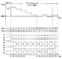
- FIG. 2 is a timing chart showing an A / D conversion operation in the first embodiment.
- FIG. 3 is a timing chart showing an A / D conversion operation in the A / D converter of the first modification.
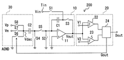
- FIG. 4 is a circuit diagram illustrating a schematic configuration of the A / D converter according to the second embodiment.
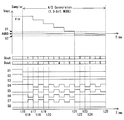
- FIG. 5 is a timing chart showing an A / D conversion operation in the second embodiment.
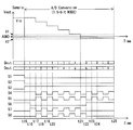
- FIG. 6 is a timing chart showing an A / D conversion operation in the A / D converter of Modification 2.
- FIG. 1 is a circuit diagram showing a schematic configuration of the A / D converter according to the first embodiment.
- FIG. 2 is a timing chart showing an A / D conversion operation in the first embodiment.
- FIG. 3 is a timing chart showing an A / D conversion operation in the A / D converter of the first modification.
- FIG. 4 is a circuit diagram illustrating
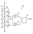
- FIG. 7 is a circuit diagram showing a configuration of a quantizer in Modification 3.
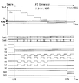
- FIG. 8 is a timing chart showing an A / D conversion operation in the A / D converter of Modification 3.
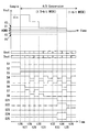
- FIG. 9 is a timing chart showing an A / D conversion operation in the A / D converter of the fourth modification.
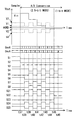
- FIG. 10 is a timing chart showing an A / D conversion operation in the A / D converter of the modification 5.
- FIG. 11 is a circuit diagram illustrating a schematic configuration of an A / D converter according to the third embodiment.
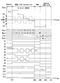
- FIG. 12 is a timing chart showing an A / D conversion operation in the third embodiment.
- FIG. 13 is a circuit diagram illustrating a schematic configuration of the A / D converter according to the fourth embodiment.
- FIG. 14 is a timing chart showing an A / D conversion operation in the fourth embodiment.
- the A / D converter 100 includes an integrator 10, a quantizer 20, and a D / A converter 30 (hereinafter referred to as DAC 30).
- the input signal (Vin) is an analog signal
- the signal (Dout) output from the A / D converter 100 is a digital signal.
- the D / A converter is a digital-to-analog converter and is also called a DAC.
- the integrator 10 includes an operational amplifier 11, an integration capacitor C1, and a feedback switch S3.
- the integration capacitor C ⁇ b> 1 is inserted between the inverting input terminal and the output terminal of the operational amplifier 11.
- the feedback switch S3 is inserted between the integration capacitor C1 and the output terminal of the operational amplifier 11. That is, the integration capacitor C1 and the feedback switch S3 are connected in series with each other and are disposed between the inverting input terminal and the output terminal of the operational amplifier 11.
- the non-inverting input terminal of the operational amplifier 11 is connected to the analog ground level (AGND).
- AGND is a reference potential of the entire A / D converter 100 and is not necessarily 0V.
- the 1st input terminal as described in a claim corresponds to the inverting input terminal in this embodiment.
- the inverting input terminal of the operational amplifier 11 can be connected to AGND via the switch S2.
- the input terminal Tin of the A / D converter 100 is connected between the integration capacitor C1 and the feedback switch S3 via the switch S1.
- the switch S1 and the switch S2 By turning on the switch S1 and the switch S2 while the feedback switch S3 is turned off, charges based on the magnitude of the input signal Vin are accumulated in the integration capacitor C1. That is, the input signal Vin is sampled in the integration capacitor C1.
- the potential of the input analog signal is referred to as the input signal Vin or simply Vin
- the potential of the output terminal of the operational amplifier 11 is referred to as the output voltage Vout or simply Vout.
- the feedback switch S3 When the switch S1 and the switch S2 are turned off and the feedback switch S3 is turned on, the output voltage Vout of the operational amplifier 11 and the potential at one end on the input side of Vin in the integration capacitor C1 become equal.
- the feedback switch S3 may be simply referred to as a switch S3.
- the quantizer 20 receives the output of the integrator 10, that is, the output voltage Vout of the operational amplifier 11, and outputs Qout which is a result of quantizing the output voltage Vout. That is, the quantizer 20 quantizes the analog value Vout and converts it into a quantization result Qout that is a digital value. Further, the quantizer 20 outputs Dout that is a result of A / D conversion of the input signal Vin.
- the quantizer 20 includes a comparator 21 and a logic circuit 24.
- the output voltage Vout of the operational amplifier 11 is input to the non-inverting input terminal, and AGND is input to the inverting input terminal.
- the output of the comparator 21 is input to the logic circuit 24.
- the logic circuit 24 outputs the quantization result Qout to the DAC 30 based on the output of the comparator 21 and outputs the A / D conversion result Dout.
- the quantization result described in the claims corresponds to Qout.
- the logic circuit 24 outputs 1 as the quantization result Qout when Vout ⁇ AGND.
- Vout ⁇ AGND ⁇ 1 is output as Qout. That is, the quantizer 20 in the present embodiment is a 1-bit quantizer.
- the logic circuit 24 sequentially integrates Qout each time quantization is performed by the quantizer 20 during the A / D conversion process, and generates an A / D conversion result Dout. More specific operation of the quantizer 20 will be described in detail later.
- the DAC 30 is a D / A converter, and determines the amount of charge that the DAC 30 subtracts from the integration capacitor C1 based on the quantization result Qout output from the quantizer 20.
- the DAC 30 has a DAC capacity C2.
- a voltage source for generating AGND and a reference voltage is connected to one end of the DAC capacitor C2 via switches S6 to S8.
- AGND is connected to one end of the DAC capacitor C2 via the switch S6,
- Vm is connected via the switch S7, and
- Vp is connected via the switch S8.
- the potential at one end of the DAC capacitor C2 is equal to any one of Vp, Vm, and AGND selected exclusively by the switches S6 to S8.
- the potential at one end of the DAC capacitor C2 may be referred to as a DAC voltage Vdac.
- one end on the inverting input terminal side of the operational amplifier 11 in the DAC capacitor C2 can be connected to AGND via the switch S4.
- the DAC capacitor C2 is connected to the inverting input terminal of the operational amplifier 11 through the switch S5. That is, the DAC 30 is connected to the integrator 10 via the switch S5.
- the charge based on the reference voltage selected by the switch S7 or the switch S8 is accumulated in the DAC capacitor C2 by turning off the switch S5 and turning on the switch S4. Further, in a state where charges are accumulated in the DAC capacitor C2, the switch S4 is turned off and the switch S5 is turned on, so that the DAC capacitor C2 is connected to the integrator 10, the switch S7 and the switch S8 are turned off, and the switch By turning on S6, the charge accumulated in the DAC capacitor C2 is transferred to the integration capacitor C1. That is, the charge accumulated in the integration capacitor C1 is subtracted by the DAC 30.
- AGND is also connected to the DAC capacitor C2 via the switch S6.
- the charge accumulated in the DAC capacitor C2 is determined based on the potential difference between Vp-AGND or Vm-AGND.
- AGND is 0 V
- the charge accumulated in the DAC capacitor C2 is determined by the magnitude of Vp or Vm, and AGND is not used as a reference voltage for substantial D / A conversion.
- FIG. 2 is a timing chart showing the operation of the A / D converter 100.
- the period before time t1 corresponds to a sampling period, and the period after time t1 corresponds to an A / D conversion period.
- both terminals of the DAC capacitor C2 are connected to AGND, respectively.
- the DAC capacitor C2 is in a state where no charge is accumulated, and is in a so-called reset state. Note that the DAC capacitor C2 is not necessarily required to perform a reset operation because charges are accumulated based on the value of the quantization result Qout after time t1.
- Vout is a value larger than AGND that is the threshold voltage of the comparator 21 constituting the quantizer 20 from time t1 to time t3.
- the switch S4 is turned off and the switch S5 is turned on, and the switch S7 is turned off and the switch S6 is turned on.
- the operation from time t2 to time t4 is one cycle related to the first charge subtraction from the integration capacitor C1.
- one cycle related to subtraction similar to that from time t2 to time t4 may be referred to as a subtraction cycle.
- the operational amplifier 11 From time t3 to time t5, the operational amplifier 11 performs the remaining A / D conversion generated as a result of the first subtraction performed by the DAC 30 from the initial Vout from time t1 to time t3 corresponding to the result of sampling the input signal Vin. The difference is output as Vout.
- Vout, Qout, and Dout are shown to change and stabilize immediately at time t3. However, in actual operation, they are accompanied by operations of an integrator, a switch, a quantizer, and the like. Due to the delay, a certain time is required until the quantization result is stably determined after Vout starts to change at time t3.
- the operation from time t1 to time t3 and from time t3 to time t5 is one cycle related to quantization by the quantizer 20.
- one cycle related to the same quantization may be referred to as a quantization cycle.
- a resolution of 3 bits (9 gradations) of A / D conversion is obtained by 8 cycles of quantization up to time t13 and 7 cycles of subtraction.
- the A / D conversion may be terminated at time t13.
- the subtraction and the quantization are further performed for each cycle to make the A / D conversion resolution 4 bits (16 gradations). Is working.
- the ninth quantization which is the last quantization, is executed.
- the value of Dout becomes the final A / D conversion result of the input signal Vin.
- the charge subtraction from the integration capacitor C1 and the quantization by the quantizer 20 are executed for a predetermined number of cycles at which a desired resolution can be obtained regardless of the level of the input signal Vin.
- the desired resolution of the A / D converter 100 is N bits, 2N-1 cycles are required for charge subtraction, and 2N-1 + 1 cycles are required for quantization.
- the A / D converter 100 is configured such that the integration capacitor C1 is disconnected from the output terminal of the operational amplifier 11 during sampling and the input signal Vin can be input to the integration capacitor C1, resetting of the integration capacitor C1 is unnecessary.
- the effects of thermal noise and flicker noise are accumulated in resetting the integration capacitor, sampling in the sampling capacitor, and transferring signal charges from the sampling capacitor to the integration capacitor.
- the integration capacitor is not used so as not to saturate the output signal of the integrator.
- the sampling capacity needs almost the same capacity value.
- the sampling capacitor is unnecessary, and the area of the capacitive element that requires a relatively large area when realized as a semiconductor integrated circuit is approximately halved. Can be reduced.
- the A / D converter 100 is a Nyquist A / D converter that performs one A / D conversion for one sampling. For this reason, a general delta-sigma A / D converter that requires oversampling does not require a high-speed buffer that is often required in the preceding stage. Therefore, there is little restriction on the conversion frequency due to the sampling speed, and high-speed and high-precision A / D conversion can be realized.
- a / D conversion can be realized with a simple configuration as compared with a SAR type A / D converter using many capacitive elements and a higher-order delta-sigma type A / D converter using a plurality of integrators. it can.
- the subtraction of a predetermined number of cycles according to the desired A / D conversion resolution is performed without depending on the level of the input signal Vin. That is, even if the output voltage Vout of the operational amplifier 11 exceeds once from the side larger than AGND by the subtraction or decreases from the side smaller than AGND to the larger side, the subtraction is continued until the predetermined number of cycles is reached.
- the magnitude of the A / D conversion error caused by the offset of the operational amplifier depends on the level of the input signal. Therefore, a non-linearity error may occur in A / D conversion.
- the A / D converter 100 executes the same number of subtractions without depending on the input level. For this reason, there is no dependency on the input level of the A / D conversion error caused by the offset of the operational amplifier 11 or the like. That is, highly accurate A / D conversion with few nonlinear errors can be realized.
- Modification 1 When adopting the two-level DAC 30 as described in the first embodiment, in addition to the method of subtracting charges using the potential difference between Vp and AGND or the potential difference between Vm and AGND as in the first embodiment. A method of subtracting using the potential difference between Vp and Vm can also be adopted.
- the operations of the switches S6 to S8 are changed with respect to the first embodiment. Specifically, the switch S6 is maintained in the OFF state from time t2 to time t14 including the period of the subtraction cycle, and either the switch S7 or the switch S8 is exclusive according to the output Qout of the quantizer 20 Thus, the switch is turned on in the first half of the subtraction cycle, and in the second half of the subtraction cycle, the on and off of the switches S7 and S8 are controlled so as to be reversed from the first half of the subtraction cycle.
- the charge is transferred from the DAC capacitor C2 to the integration capacitor C1, and a voltage corresponding to the residual of A / D conversion is output as the output voltage Vout of the operational amplifier 11.
- the DAC 30 in the present modification is not used for subtraction involving the change in Vout by the DAC 30 because the switch S6 is maintained in the OFF state from time t2 to time t14 as compared to the first embodiment. For this reason, in the case where the present modification is implemented with a single-ended circuit configuration, even if an error occurs between the intermediate potential between Vp and Vm and the potential of AGND, it is caused by subtraction of charges from the integration capacitor C1. A / D conversion offset error does not occur. That is, the demand for the accuracy of the power source that generates Vp, Vm, and AGND can be relaxed compared to the first embodiment.
- the A / D converter 200 includes an integrator 10, a quantizer 20, and a D / A converter 30 (hereinafter referred to as DAC 30).
- the input signal (Vin) is an analog signal
- the signal (Dout) output from the A / D converter 200 is a digital signal.
- the A / D converter 200 in the present embodiment is different from the A / D converter 100 in the first embodiment in the configuration of the quantizer 20. Since the integrator 10 has the same configuration as that of the first embodiment, detailed description thereof is omitted.
- the DAC 30 is different from the first embodiment in the specification of the input signal, that is, the DAC voltage Vdac corresponding to the output Qout of the quantizer 20. This will be described in detail below.
- the quantizer 20 in this embodiment receives the output of the integrator 10, that is, the output voltage Vout of the operational amplifier 11, and outputs Qout that is the result of quantizing the Vout. That is, the quantizer 20 quantizes the analog value Vout and converts it into a quantization result Qout that is a digital value. Further, the quantizer 20 outputs Dout that is a result of A / D conversion of the input signal Vin.
- the quantizer 20 includes a first comparator 22, a second comparator 23, and a logic circuit 24.
- the output voltage Vout of the operational amplifier 11 is input to the non-inverting input terminal, and the threshold voltage V1 is input to the inverting input terminal.
- the second comparator 23 receives the output voltage Vout of the operational amplifier 11 at the non-inverting input terminal and the threshold voltage V2 at the inverting input terminal.
- the threshold voltage V1 is higher than AGND, and the threshold voltage V2 is lower than AGND. That is, each voltage has a relationship of V2 ⁇ AGND ⁇ V1.
- the outputs of the comparators 22 and 23 are input to the logic circuit 24, respectively. Based on the outputs of the comparators 22 and 23, the logic circuit 24 outputs a quantization result Qout to the DAC 30 and outputs a digital signal Dout as an A / D conversion result.
- the logic circuit 24 outputs 1 as the quantization result Qout when Vout> V1.
- V2 ⁇ Vout ⁇ V1, 0 is output as Qout.
- Vout ⁇ V2, ⁇ 1 is output as Qout. That is, the quantizer 20 in the present embodiment is a 1.5-bit quantizer.
- the logic circuit 24 sequentially integrates Qout each time quantization is performed by the quantizer 20 during the A / D conversion process, and generates an A / D conversion result Dout. The specific operation of the quantizer 20 will be described in detail later.
- the DAC 30 is a D / A converter, and determines the amount of charge that the DAC 30 subtracts from the integration capacitor C1 based on the quantization result Qout output from the quantizer 20.
- This DAC 30 has, as reference voltages, a three-level D / A having an analog ground level AGND, a high level Vp set to a potential higher than AGND, and a low level Vm set to a potential lower than AGND. It is a converter.
- FIG. 5 is a timing chart showing the operation of the A / D converter 200.
- the period before time t15 corresponds to a sampling period, and the period after time t15 corresponds to an A / D conversion period.
- the switch S1 and the switch S2 are turned off and the switch S3 is turned on, whereby the output voltage Vout of the operational amplifier 11 becomes the same voltage value as Vin, and Vin is held in the integration capacitor C1.
- Vout is larger than the threshold voltage V1 of the first comparator 22 constituting the quantizer 20.
- the switch S4 is turned off and the switch S5 is turned on, and the switch S7 is turned off and the switch S6 is turned on.
- the operational amplifier 11 From the time t17 to the time t19, the operational amplifier 11 performs the remaining A / D conversion generated as a result of performing the first subtraction by the DAC 30 from the initial Vout at the time t15 to the time t17 corresponding to the result of sampling the input signal Vin. The difference is output as Vout.
- the A / D converter 200 in the present embodiment also has the same effect as that of the first embodiment.
- the quantizer 20 in this embodiment functions as a 1.5-bit quantizer, a quantization cycle corresponding to the last quantization cycle shown in FIG. 2 is required as the first embodiment.
- a / D conversion with a resolution of 4 bits (17 gradations) can be realized by quantization of 8 cycles.
- Modification 2 When adopting the three-level DAC 30 as described in the second embodiment, a method of subtracting using a potential difference between Vp-AGND or Vm-AGND during the A / D conversion period as in the second embodiment, a method of subtracting by using a potential difference between Vp-Vm or Vm-Vp can be employed as in the first modification.
- the operations of the switches S6 to S8 are changed with respect to the second embodiment. Specifically, at time t16, the switch S6 is turned off and the switch S7 is turned on. At time t17, the switch S7 is turned off, and the switch S8 is turned on while maintaining the off state of the switch S6.
- a corresponding voltage is output as the output voltage Vout of the operational amplifier 11.
- the DAC 30 in the present modification is not used for subtraction involving change in Vout by the DAC 30 because the switch S6 is maintained in the OFF state from time t16 to time t22 as compared to the second embodiment.
- AGND is connected to the DAC capacitor C2 via the switch S6, but no substantial subtraction is performed.
- the present modification is implemented with a single-ended circuit configuration, even if an error occurs between the intermediate potential between Vp and Vm and the potential of AGND, the error at the time of subtracting the charge from the integration capacitor C1
- the resulting offset error or nonlinearity error of A / D conversion does not occur. That is, the demand for the accuracy of the power source that generates Vp, Vm, and AGND can be relaxed compared to the second embodiment.
- Modification 3 In the second embodiment and the second modification, a mode has been described in which the quantizer 20 is configured by two comparators 22 and 23 to realize 1.5-bit quantization. On the other hand, in this modification, a mode will be described in which the threshold voltage of the comparators 22 and 23 is made variable so that the resolution of the quantizer is switched between 1.5 bits and 1 bit.
- the threshold voltage input to the first comparator 22 can be changed in three ways: V1, V3, and V5. Further, the threshold voltage input to the second comparator 23 can be changed in two ways, V2 and V4. Specifically, as shown in FIG. 7, resistors R1 to R6 are connected in series in the order of R1 to R6 from the higher potential between the high level Vp and the low level Vm. The point potential can be input to the comparators 22 and 23 as a threshold voltage.
- each of the resistors R1 to R6 is set so that the voltage V3 is generated at the midpoint between the resistors R1 and R2, and is set so that the voltage V1 is generated at the midpoint between the resistors R2 and R3.
- the voltage V5 is set at the midpoint between the resistors R3 and R4, and the voltage V2 is set at the midpoint between the resistors R4 and R5.
- the resistor R5 and the resistor The voltage V4 is set to be generated at the midpoint of R6.
- the voltage V3 can be input to the inverting input terminal of the first comparator 22 via the switch S21, the voltage V1 can be input via the switch S22, and the voltage V5 can be input via the switch S23.
- the voltage V2 can be input to the inverting input terminal of the second comparator 23 via the switch S24, and the voltage V4 can be input via the switch S25.
- the quantizer 20 in the present modification can set five types of V1 to V5 as threshold voltages of the comparators 22 and 23, but the operation of the present modification is configured to use only three types. Examples of setting five types of voltages will be described in Modifications 4 and 5 described later.
- the operation up to time t25 is the same as that of the second embodiment, except that subtraction based on Qout immediately before time t25 is executed. That is, the difference is that 2N-1 cycles of subtraction are executed when the resolution of A / D conversion in the period up to time t25 is N bits. Since the other points are the same operation, the description thereof is omitted.
- the threshold voltage in the quantizer 20 is set to V1 and V2. That is, the switch S22 and the switch S24 are turned on, and the switches S21, S23, and S25 are turned off. Thereby, the quantizer 20 in the present modification functions as a 1.5-bit quantizer until time t25. In FIG. 8, this A / D conversion period is described as 1.5-bit MODE (1.5-bit mode).
- the switch S22 in the quantizer 20 shown in FIG. 7 is turned off, and the switch S23 is turned on.
- the threshold voltage input to the second comparator 23 is maintained at V2, but the logic circuit 24 in this modification is set to ignore the comparison result of Vout and V2. That is, after time t25, the quantizer 20 in this modification functions as a 1-bit quantizer that uses only the first comparator 22 whose threshold voltage is AGND.
- the last quantization is executed by the quantizer 20 whose resolution is set to 1 bit. Since one threshold voltage V5 used for the last quantization is exactly between the two threshold voltages V1 and V2 used for the quantization before time t25, the resolution of the A / D conversion is set to 1 bit by the last quantization. Can be increased by minutes. For this reason, the logic circuit 24 calculates Dout immediately before time t25 by a factor of 2, and then adds the 1-bit quantization result Qout.
- a / D conversion with a resolution of 5 bits (32 gradations) is performed by quantization of 9 cycles and subtraction of 8 cycles.
- the desired resolution of the A / D converter is N bits
- subtraction of charge requires 2N-2 cycles and quantization requires 2N-2 + 1 cycles.
- the number of cycles necessary to obtain the same resolution as that of the second modification is substantially halved.
- Modification 4 In the third modification, the mode in which the resolution of the A / D converter is improved by changing the resolution using three types of threshold voltages in the quantizer 20 shown in FIG. 7 has been described. In the present modification, a mode in which the resolution is further improved by changing the resolution of the quantizer 20 using five types of threshold voltages in the quantizer 20 shown in FIG. 7 will be described.
- the threshold voltage of the first comparator 22 in the quantizer 20 is set to V3, and the threshold voltage of the second comparator 23 is set to V4. That is, the switch S21 and the switch S25 are turned on, and the switches S22 to S24 are turned off. That is, between time t26 and time t31, the difference between the two threshold voltages is set larger than that in the second embodiment.
- the switch S6 is turned off and the switch S7 is turned on as in the second modification.
- the switch S7 is turned off, and the switch S8 is turned on while maintaining the off state of the switch S6.
- the switch S21 is turned off and the switch S22 is turned on. That is, the threshold voltage of the first comparator 22 of the quantizer 20 is switched from V3 to V1.
- the switch S25 is turned off and the switch S24 is turned on. That is, the threshold voltage of the second comparator 23 of the quantizer 20 is switched from V4 to V2.
- Vout does not change between time t32 and time t34, but subtraction is performed in a state where the DAC voltage Vdac is set to AGND as in the second modification.
- a / D conversion resolution 4 bits (17 gradations) of A / D conversion resolution can be obtained by time t35 when quantization of 5 cycles is completed.
- the quantization until obtaining the same A / D conversion result Dout as in the second embodiment is 5 cycles, which is more than the 8 cycles in the second embodiment.
- the quantizer 20 is operated in the 1-bit mode after the time t35 and the last quantization is executed in the same manner as the time t25 and after in the modification 3.
- Dout 9 which is the final A / D conversion result of the input signal Vin is obtained.
- the resolution of A / D conversion is 5 bits (32 gradations) by 6 cycles of quantization and 5 cycles of subtraction. If the desired resolution of the A / D converter is N bits, charge subtraction requires 2N-3 + 1 cycles and quantization requires 2N-3 + 2 cycles. Therefore, when the resolution N is high, the number of cycles required to obtain the same resolution as in the third modification can be reduced to approximately half. Further, by reducing the number of subtraction cycles, it is possible to reduce the influence of thermal noise and flicker noise that increase due to the execution of subtraction on the A / D conversion result.
- the quantizer 20 in the present modification functions as a 1.5-bit quantizer, although the two threshold voltages of the quantizer 20 are changed at time t33 in the period from time t26 to time t35, respectively. is doing. Further, after time t35, it functions as a 1-bit quantizer with a threshold voltage of AGND.
- the quantizer 20 of the A / D converter 200 uses the quantization result Qout of each half-quantization cycle by changing the threshold voltage for each half-quantization cycle during one-cycle quantization. To control the DAC 30. That is, a 1.5-bit quantizer 20 is used to perform five-level quantization in one quantization cycle, thereby realizing a substantially 2.5-bit quantizer.
- the threshold voltage of the first comparator 22 is V3 and the threshold voltage of the second comparator 23 is V4, and in the second half of the quantization cycle, the first comparator The threshold voltage of 22 is set to V1, the threshold voltage of the second comparator 23 is set to V2, and two quantizations are executed within one quantization cycle.
- the DAC 30 performs control using each of two quantization results in one quantization cycle.
- the DAC voltage Vdac for driving the DAC 30 is determined based on the total value of Qout in one quantization cycle. Specifically, if the total value of two quantization results Qout in one quantization cycle is 2, subtraction is performed with the potential difference between the first half and the second half of one subtraction cycle of the DAC voltage Vdac as Vp ⁇ Vm. Similarly, if the total value of Qout is 1, the potential difference is Vp ⁇ AGND, if the total value of Qout is ⁇ 1, the potential difference is Vm ⁇ AGND, and if the total value of Qout is ⁇ 2, the potential difference is Vm ⁇ AGND. Subtraction is performed as Vp. If the total value of Qout is 0, the DAC voltage Vdac is set to AGND and substantially no subtraction is performed.
- the total value of Qout is 2, Vout> V3 and Vout> V1, and in the subtraction cycle between time t40 and time t42, subtraction by the potential difference Vp ⁇ Vm. Is executed.
- the DAC voltage Vdac in the first half of the subtraction cycle is determined from only Qout in the second half of the quantization cycle, and the second half of the quantization cycle.
- the DAC 30 may be operated by determining the DAC voltage Vdac in the second half of the subtraction cycle from only Qout.
- the total value 2 of the two Qouts from time t37 to time t39 is reflected in the subtraction in the subtraction cycle from time t38 to time t40. That is, in the subtraction cycle from time t38 to time t40, the switches S6 to S8 are controlled based on Qout obtained between time t37 and time t39, and the subtraction is executed.
- the resolution of 5-bit (32 gradations) A / D conversion is obtained by 5 quantization cycles and 4 subtraction cycles. If the desired resolution of the A / D converter is N bits, charge subtraction requires 2N-3 cycles and quantization requires 2N-3 + 1 cycles. Therefore, when the desired resolution N is high, the number of cycles required to obtain the same resolution as that of the third modification can be reduced to almost half. Further, similarly to the fourth modification, it is possible to reduce the influence of thermal noise and flicker noise that increase due to execution of subtraction.
- the A / D converter 300 in this embodiment is configured to execute a part of the quantization in the A / D conversion process by an A / D converter different from the quantizer 20.
- an A / D converter different from the quantizer 20 is referred to as a secondary ADC 50.
- the secondary ADC is also referred to as a secondary analog-to-digital converter or another ADC.
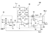
- the A / D converter 300 in this embodiment includes a sub ADC 50 and an adder 60 in addition to the integrator 40, the quantizer 20, and the DAC 30. Since the DAC 30 is the same as that of the fifth modification of the second embodiment, a detailed description thereof is omitted. Also, in FIG. 11, the detailed configuration is omitted for the sake of simplification, but the quantizer 20 uses the variable threshold voltage shown in FIG. 7 as in the fifth modification of the second embodiment. It is.
- the integrator 40 has an integration capacitor C1 and an amplification capacitor C3, which are connected in parallel between the inverting input terminal and the output terminal of the operational amplifier 11.
- the integration capacitor C1 has one end connected to the inverting input terminal of the operational amplifier 11 via the switch S9 and the other end connected to the output terminal of the operational amplifier 11 via the switch S3.
- the middle point of the integrating capacitor C1 and the switch S9 is connected to AGND via the switch S2, and the middle point of the integrating capacitor C1 and the switch S3 is connected to AGND via the switch S10.
- the amplification capacitor C3 has one end connected to the inverting input terminal of the operational amplifier 11 via the switch S14 and the other end connected to the output terminal of the operational amplifier 11 via the switch S12.
- the middle point of the amplification capacitor C3 and the switch S14 is connected to AGND via the switch S13, and the middle point of the amplification capacitor C3 and the switch S12 is connected to AGND via the switch S11.
- the input terminal Tin is connected to the middle point of the integration capacitor C1 and the switch S3 via the switch S1.
- the functions of the switches S2 and S3 are the same as those of the switches S2 and S3 in the second embodiment, respectively.
- the secondary ADC 50 is connected to the output terminal of the operational amplifier 11 in parallel with the quantizer 20.
- the digital output Lout of the secondary ADC 50 is input to the adder 60 together with the digital output Mout of the quantizer 20.
- the adder 60 adds Mout output from the quantizer 20 and Lout output from the sub ADC 50 to obtain a final digital output Dout.
- a generally known A / D converter can be adopted as the secondary ADC 50.
- the switches S1, S2, S4, S6, S11, and S13 are turned on, and the switches S3, S5, S7, S8, S9, S10, S12, and S14 are turned off. Since the switch S3 is off, the integration capacitor C1 and the output terminal of the operational amplifier 11 are electrically separated from each other. Since the switches S1 and S2 are on, the input signal Vin is sampled by the integration capacitor C1. Further, since the switches S11 and S13 are turned on and the switches S12 and S14 are turned off, the amplification capacitor C3 is electrically separated from the operational amplifier 11, and both ends thereof are connected to AGND. As a result, the amplification capacitor C3 is in a state where no charge is accumulated.
- both terminals of the DAC capacitor C2 are connected to AGND, respectively. As a result, the DAC capacitor C2 is in a state where no charge is accumulated.
- the resolution of A / D conversion obtained in Mout is 4 bits (17 gradations), and the upper 4 bits of the A / D conversion result Dout of this embodiment are converted by the quantizer 20 to A / D D-converted.
- the switches S3, S11, and S13 are turned off, and the switches S10, S12, and S14 are turned on and the last subtraction is performed. Thereby, all charges corresponding to the residual of A / D conversion are transferred to the amplification capacitor C3.
- the sub ADC 50 After time t49, the sub ADC 50 performs A / D conversion on the amplified residual Vout output from the operational amplifier 11.
- the final A / D conversion result Mout corresponding to the upper 4 bits by the quantizer 20 and the A / D conversion result Lout corresponding to the lower 4 bits by the sub ADC 50 are added to obtain the final A An 8-bit resolution is obtained for the / D conversion result Dout.
- the sub ADC 50 performs A / D conversion of lower bits using the residual of the A / D conversion related to the previous A / D conversion as an input. Has been. That is, the A / D conversion of the lower bits related to the previous A / D conversion and the sampling of the input signal Vin related to the next A / D conversion are performed in parallel.
- the A / D converter 300 includes a sub ADC 50 that performs A / D conversion of lower bits. For this reason, the resolution of the A / D conversion of the upper bits by the quantizer 20 whose number of cycles exponentially increases with increasing resolution is reduced, and the number of cycles required for A / D conversion is greatly reduced. can do.
- the A / D converter 300 in the present embodiment has an amplification capacitor C3 as a separate body from the integration capacitor C1. For this reason, during the operation of the A / D conversion of the lower bits by the sub ADC 50, the sampling for the next A / D conversion can be executed in parallel by separating the integration capacitor C1 from the operational amplifier 11. Further, since the secondary ADC 50 is not used for the next A / D conversion even in the A / D conversion period of the higher bit related to the next A / D conversion after time t51, the previous ADC is used by using the secondary ADC 50. A / D conversion of lower bits related to / D conversion can be executed. For this reason, it is easy to secure the processing time of the sampling of the input signal Vin and the A / D conversion of the lower bits by the sub ADC 50, and the overall throughput of the A / D conversion can be improved.
- a general A / D converter can be used for the secondary ADC 50.
- a Nyquist A / D converter that performs A / D conversion by sampling once to increase the conversion speed is used as the secondary ADC 50, the entire A / D conversion is not required without requiring high-precision techniques such as trimming.
- a / D conversion of lower bits up to about 10 to 12 bits can be assigned to the sub ADC 50 while maintaining the conversion accuracy. Therefore, in the present embodiment, the number of A / D conversion cycles of the upper bits by the quantizer 20 is significantly reduced while suppressing an increase in A / D conversion error caused by the conversion accuracy of the sub ADC 50. As a result, the speed of A / D conversion can be greatly improved.
- the non-linearity error of A / D conversion caused by the ratio accuracy between the DAC capacitor C2 and the amplification capacitor C3 can be reduced by increasing the resolution of the A / D conversion of the upper bits by the quantizer 20. Therefore, by assigning a resolution that is sufficiently smaller than the accuracy corresponding to the resolution assigned to the sub ADC 50 to the A / D conversion of the upper bits, the nonlinearity error of the A / D conversion of the upper bits is reduced. The influence on the accuracy of the entire A / D conversion can be sufficiently reduced.
- the resolution of the entire A / D conversion is 16 bits
- a resolution of 10 to 12 bits is assigned to the sub ADC 50 for the A / D conversion of the lower bits, and 4 for the A / D conversion of the upper bits by the quantizer 20. Allocate a resolution of ⁇ 6 bits.
- the A / D converter 400 in this embodiment includes an integrator 70, a quantizer 20, a DAC 30, a secondary ADC 50, and an adder 60. Since the DAC 30 is the same as that of each of the above-described embodiments and modifications, detailed description thereof is omitted.
- the quantizer 20 is the same as that in the third embodiment.
- the integrator 70 in this embodiment has a switch S10 in addition to the integrator 10 in the second embodiment.
- the switch S10 is interposed between the integration capacitor C1, the midpoint of the switch S3, and AGND. Since the switch S10 has the same operation and function as the switch S10 in the third embodiment, it is denoted by the same reference numerals as in the third embodiment.
- the output terminal of the operational amplifier 11 in the integrator 70, the switches S6 to S8 in the DAC 30, and the midpoint of the DAC capacitor C2 are connected via the switch S15. It is connected. Therefore, by turning on the switches S5, S10, and S15 after turning off the switches S1 to S4 and the switches S6 to S8, the charge of the integration capacitor C1 can be transferred to the DAC capacitor C2.
- the A / D converter 400 in this embodiment has the same configuration as the A / D converter 300 in the third embodiment except for the integrator 70 and the switch S15.
- the switch S4 is turned off and the switch S5 is turned on, and the final subtraction is executed.
- the switch S5 is turned off, the switch S4 is turned on, and the switch S6 is turned on, so that the charge of the DAC capacitor C2 is reset.
- the switch S6 is turned off and the switches S10 and S15 are turned on.
- the A / D conversion residual amplification is performed simultaneously with the final subtraction.
- the residual amplification is performed using the DAC capacitor C2 used for the subtraction.
- the charge of the DAC capacitor C2 is reset, and the amplification of the residual is started after time t55.
- the amplified residual of A / D conversion is transferred to the sub ADC 50.
- the transferred residual is A / D converted by the sub ADC 50 after time t55.
- the switches S10 and S15 are turned off and the switch S6 is turned on.
- the switch S1 and the switch S2 are turned on while the switch S3 is in an off state, sampling for the next A / D conversion is started using the integration capacitor C1 as before time t52.
- time t57 is a period of A / D conversion of the upper bits by the quantizer 20 related to the next A / D conversion
- the operation of the A / D converter 400 is the same as the period from the time t52 to the time t56. is there.
- the secondary ADC 50 is not used for the next A / D conversion executed after time t56. That is, in the period from time t56 to time t59, the lower bit A / D conversion related to the previous A / D conversion, the sampling of the input signal Vin related to the next A / D conversion, and the upper bit A / D conversion are performed.
- the D conversion is executed in parallel.
- the A / D converter 400 in this embodiment includes a sub ADC 50 that performs A / D conversion of lower bits. For this reason, as in the third embodiment, the number of cycles required for A / D conversion of the upper bits by the quantizer 20 can be reduced.
- the A / D converter 400 when the transfer of the residual of the A / D conversion to the sub ADC 50 is completed, the A / D of the lower bits by the sub ADC 50 as in the third embodiment. In parallel with the conversion, the sampling for the next A / D conversion and the A / D conversion of the upper bits can be performed. Therefore, the throughput of A / D conversion can be improved.
- the DAC capacitor C2 of the present embodiment is configured so as to also function as the amplification capacitor C3 of the third embodiment. For this reason, the number of necessary capacitive elements can be reduced, and non-linearity errors in A / D conversion due to the ratio accuracy of the capacitance value between the DAC capacitor C2 and the amplification capacitor C3 do not occur.
- a / D conversion with a predetermined number of bits such as 4 bits or 8 bits has been described as an example.
- the A / D converters 100 to 400 may have any number of bits. It is applicable to.
- each switch operates so as to reset the DAC capacitor C2 or the amplification capacitor C3 during the sampling period of the input signal Vin is described. Any design can be made without departing from the gist of the present disclosure.
- the single-ended operational amplifier 11 is used as an amplifier has been described for the sake of simplicity.
- the A / D converters 100 to 400 are configured using a differential operational amplifier instead of the single-ended operational amplifier. You can also
Landscapes
- Engineering & Computer Science (AREA)
- Theoretical Computer Science (AREA)
- Analogue/Digital Conversion (AREA)
- Compression, Expansion, Code Conversion, And Decoders (AREA)
Abstract
A/D変換器は、第1入力端子と出力端子を備えるオペアンプ(11)と積分容量(C1)とを有する積分器(10)と、オペアンプの出力信号を量子化した量子化結果を出力する量子化器(20)と、第1入力端子に接続され、DAC電圧を決定するDAC(30)と、を備える。積分器は、積分容量とオペアンプの出力端子との間にフィードバックスイッチ(S3)を有する。入力信号としてのアナログ信号は、積分容量とフィードバックスイッチとの間に入力される。積分容量は、アナログ信号をサンプリングする。量子化器がオペアンプの出力に基づいて量子化を行う。DACが積分容量に蓄積された電荷を順次減算することによりアナログ信号をデジタル値に変換する。
Description
本出願は、2015年9月3日に出願された日本国特許出願2015-173922号に基づくものであり、ここにその記載内容を参照により援用する。
本開示は、簡素な構成で、高速かつ高精度なA/D変換を実現できるA/D変換器に関する。
環境問題やエネルギー問題を背景に、自動車や産業機器をより高速かつ高精度に制御して排出ガスを抑制したり、使用するエネルギー量を低減したりすることへの要求が高まっている。自動車や産業機器を制御する制御回路はデジタル化が進んでおり、機器の物理的状態を検出するセンサが出力するアナログ信号をA/D(アナログ/デジタル)変換器(ADC)によってデジタル信号に変換した上で、デジタル信号処理した結果を用いて機器を制御するのが一般的になっている。そのため、高速かつ高精度なADCに対する要求が高まっている。
例えば、特許文献1に記載の逐次比較(SAR)型のADCは、ADCを構成する容量素子の容量値の誤差に起因するA/D変換の非線形性誤差を低減するために、A/D変換を実行する際に使用する容量についてディザリングを実施するように構成されている。
一方、特許文献2および非特許文献1に記載のADCは、デルタシグマ(ΔΣ)変調を利用して高精度化を実現したデルタシグマ型A/D変換器である。
また、特許文献3に記載のA/D変換器は、アナログ量子化器によるフィードバック量の大きさを可変にした増分デルタ(インクリメンタルΔ)型のA/D変換器である。
K. C.-H. Chao,S. Nadeem, W. L. Lee, and C. G. Sodini, "A Higher Order Topology for Interpolative Modulators for Oversampling A/D Converter", IEEE Transactions on Circuits and Systems, Vol. 37, No. 3, Mar. 1990
特許文献1に記載のA/D変換器は、高精度化のためにディザリングと呼ばれる手法が用いられている。しかしながら、ディザリングは素子の誤差を時間方向に分散して誤差を見かけ上低減することはできるものの、時間方向に分散した誤差を完全に無くすことはできない。また、ディザリングを実施するためには追加の制御機構が必要であり、素子面積や消費電力が増大してしまう虞がある。
また、ディザリング以外の高精度化手法として、素子の誤差を測定した上で、素子の誤差に応じた補正値を記憶し、補正値にもとづきA/D変換結果を補正するトリミングと呼ばれる手法も広く用いられている。しかしながら、トリミングの実現には補正値を記憶するための記憶素子や記憶した補正値にもとづき補正を実行するための補正機構が追加で必要となる。
さらに、SAR型のA/D変換器で主流となっている容量DACを用いる回路構成では、高精度化のためには容量DACに用いる容量素子の比精度を高める必要があり、総容量値を比較的大きくしなければならない。このため、A/D変換の過程で大きな容量値を持つ容量DACを参照電圧によって駆動するため、参照電圧を十分に低いインピーダンスで供給できないような状況においては、参照電圧のセトリングに比較的長い時間が必要である。よって、高精度化のために容量値を大きくするほど高速化が困難になるという問題がある。
また、非特許文献1に記載のデルタシグマ型のA/D変換器では、高精度化のためにオーバーサンプリングが必要であるが、所望の信号帯域に対して1桁から2桁高い周波数でオーバーサンプリングを実行するのが一般的であり、回路の動作周波数が変換速度を律速することが多い。また、A/D変換器の前段の入力信号源が高速なオーバーサンプリングを実行するために必要な低い出力インピーダンスを持たない場合には、高速なバッファが必要となるため、バッファの動作周波数が変換速度を律速することが多い。また、オーバーサンプリングを実施し、かつ、高速化と高精度化のために高次のΔΣ変調を用いる場合には、複数の異なるサンプリング時刻における入力信号に対してフィルタ処理がかかった結果がA/D変換結果として出力される。そのため、例えばある特定の時刻の入力信号の大きさのみを用いて機器の制御を行う用途には適さない。
また、特許文献2に記載のデルタシグマ型A/D変換器のように、デルタシグマ型A/D変換器にナイキストA/D変換器を組み合わせることで、高速化と高精度化を両立させるA/D変換器も知られている。このようなA/D変換器では、ΔΣ変調によりA/D変換結果の上位ビット(MSBs)を生成し、ナイキストA/D変換器によりA/D変換結果の下位ビット(LSBs)を生成することにより、高精度化と高速化を実現している。しかしながら、このようなA/D変換器でも、前段のΔΣ変調器においてオーバーサンプリングを行うため、上述のナイキストA/D変換器を組み合わせないデルタシグマ型A/D変換器と同様に、A/D変換器の前段バッファの動作周波数が高くなる問題や、特定の時刻の入力信号のA/D変換結果が得られないという問題がある。
また、特許文献3では、上記のデルタシグマ型のA/D変換器の問題点を解決するためにデルタ変調を基本原理とする増分デルタ(インクリメンタルΔ)型A/D変換器が提案されている。このA/D変換に用いられるデルタ変調は、A/D変換に必要なサイクル数が高分解能化に伴って指数関数的に増加する問題点がある。そのため、サイクル数を低減することによりA/D変換を高速化するために、大きさが異なる複数の参照電圧を用いるDACをフィードバックに用いている。すなわち、大きい参照電圧による粗い分解能のデルタ変調と小さい参照電圧による細かい分解能のデルタ変調を組み合わせて実行することで、A/D変換に必要なサイクル数を低減している。しかしながら、参照電圧を生成する回路を構成する素子の素子値には通常誤差があるため、複数の大きさが異なる参照電圧を高い比精度で生成することは困難である。そのため、DACによるフィードバック時に誤差が発生し、高精度のA/D変換を実現することが困難である。また、粗い分解能と細かい分解能のデルタ変調を組み合わせてA/D変換に必要なサイクル数を削減しても、A/D変換に必要なサイクル数が高分解能化に伴って指数関数的に増大するという問題が残る。
また、特許文献2および非特許文献1に記載のデルタシグマ型A/D変換器の一般的な構成や、特許文献3に示されるA/D変換器では、サンプリング容量と積分器の積分容量が別の容量素子を用いて構成されるため、サンプリングにおける熱雑音を低減するためには、サンプリング容量の容量値を大きくする必要がある。さらに、熱雑音を低減するためにサンプリング容量の容量値を大きくすると、積分器の出力信号振幅の飽和を避けるために、サンプリング容量の大きさに応じて積分器の積分容量の容量値も大きくする必要があり、集積回路上に実現する場合には大きな面積が必要となる。
また、サンプリング容量から積分器への信号電荷の転送が必要なため、転送時に発生する熱雑音やフリッカー雑音の影響を低減するために、積分器を構成するオペアンプの面積や消費電力を増大して雑音を低減する必要がある。
本開示の目的は、簡素な構成で、高速かつ高精度なA/D変換を実現できるナイキストA/D変換器を提供することである。
本開示の一例にかかるA/D変換器は、第1入力端子と出力端子を備えるオペアンプと、該オペアンプの第1入力端子と出力端子との間に挿入された積分容量と、を有する積分器と、オペアンプの出力信号を量子化した量子化結果を出力する量子化器と、オペアンプにおける第1入力端子に接続され、積分容量に蓄積された電荷の減算を行うためのDAC電圧を量子化結果に基づいて決定するD/A変換器(DAC)と、を備える。積分器は、積分容量とオペアンプの出力端子との間に、互いの接続をオンオフするフィードバックスイッチを有する。入力信号としてのアナログ信号は、積分容量とフィードバックスイッチとの間に入力される。積分容量は、アナログ信号をサンプリングする。量子化器がオペアンプの出力に基づいて量子化を行う。DACが量子化結果に基づいて積分容量に蓄積された電荷を順次減算することによりアナログ信号をデジタル値に変換する。
この構成によれば、入力信号としてのアナログ信号が積分器における積分容量に一回のサンプリングにより保持され、サンプリングにより保持された電荷に基づいてA/D変換を行うので、オーバーサンプリングを必要としない。すなわち、特定の時刻の入力信号に対してA/D変換を実行するナイキストA/D変換器を構成することができる。また、オーバーサンプリングを必要としないので、回路の動作周波数が前段のバッファの動作周波数に律速されず、高速なA/D変換を実現することができる。
また、例えばDACを一つの容量を用いて構成し、かつ、DACが実質一つの参照電圧によって駆動されるように構成することで、構成要素の特性ばらつきに起因するA/D変換の誤差を抑制できる。したがって、A/D変換に用いるDACが複数の容量で構成されるSAR型のA/D変換器において、高精度化のためにしばしば行われるトリミングやディザリング等の操作を実施することなく、高精度なA/D変換を実現することができる。また、特許文献3とは異なり複数の参照電圧を用いてDACを駆動しないことから、参照電圧を発生する回路の誤差に起因するA/D変換の非線形性誤差が発生しない。
また、積分容量を用いてサンプリングを実行するため、特許文献2や非特許文献1に示されるデルタシグマ型のA/D変換器、および、特許文献3のように積分容量とサンプリング容量が別の容量で構成されるA/D変換器と比較して、サンプリング後のサンプリング容量と積分容量との間での信号電荷の転送が不要である。また、積分容量のリセットが不要なため積分容量のリセットに起因する熱雑音が発生しない。このため、高速かつ低ノイズのA/D変換を実現することができる。また、熱雑音を十分低減するために大きな容量値と面積を必要とするサンプリング容量を必要としないので、低コストにA/D変換を実現することができる。
また、特許文献1に示されるような多数の素子を要するSAR型のA/D変換器や非特許文献1に示されるような高速化のために複数の積分器を要する高次のΔΣ変調を用いたA/D変換器に較べて簡素な構成でA/D変換を実現することができる。従って、簡素な構成で、高速かつ高精度なA/D変換を実現できるナイキストA/D変換器が提供される。
本開示についての上記および他の目的、特徴や利点は、添付の図面を参照した下記の詳細な説明から、より明確になる。添付図面において
図1は、第1実施形態にかかるA/D変換器の概略構成を示す回路図であり、
図2は、第1実施形態におけるA/D変換動作を示すタイミングチャートであり、
図3は、変形例1のA/D変換器におけるA/D変換動作を示すタイミングチャートであり、
図4は、第2実施形態にかかるA/D変換器の概略構成を示す回路図であり、
図5は、第2実施形態におけるA/D変換動作を示すタイミングチャートであり、
図6は、変形例2のA/D変換器におけるA/D変換動作を示すタイミングチャートであり、
図7は、変形例3における量子化器の構成を示す回路図であり、
図8は、変形例3のA/D変換器におけるA/D変換動作を示すタイミングチャートであり、
図9は、変形例4のA/D変換器におけるA/D変換動作を示すタイミングチャートであり、
図10は、変形例5のA/D変換器におけるA/D変換動作を示すタイミングチャートであり、
図11は、第3実施形態にかかるA/D変換器の概略構成を示す回路図であり、
図12は、第3実施形態におけるA/D変換動作を示すタイミングチャートであり、
図13は、第4実施形態にかかるA/D変換器の概略構成を示す回路図であり、
図14は、第4実施形態におけるA/D変換動作を示すタイミングチャートである。
以下、本開示の実施の形態を図面に基づいて説明する。なお、以下の各図相互において、互いに同一もしくは均等である部分に、同一符号を付与する。
(第1実施形態)
最初に、図1を参照して、本実施形態に係るA/D変換器(アナログデジタル変換器)の概略構成について説明する。
最初に、図1を参照して、本実施形態に係るA/D変換器(アナログデジタル変換器)の概略構成について説明する。
図1に示すように、このA/D変換器100は、積分器10と、量子化器20と、D/A変換器30(以降、DAC30と示す)とを備えている。入力信号(Vin)はアナログ信号であり、A/D変換器100から出力される信号(Dout)はデジタル信号である。D/A変換器は、digital-to-analog Converterであり、DACとも呼ばれる。
積分器10は、オペアンプ11と、積分容量C1と、フィードバックスイッチS3と、を有している。積分容量C1は、オペアンプ11の反転入力端子と出力端子との間に挿入されている。フィードバックスイッチS3は積分容量C1とオペアンプ11の出力端子との間に挿入されている。つまり、積分容量C1とフィードバックスイッチS3は互いに直列接続されて、オペアンプ11の反転入力端子と出力端子との間に配置されている。一方、オペアンプ11の非反転入力端子はアナロググランドレベル(AGND)に接続されている。AGNDはA/D変換器100全体の基準電位であり、必ずしも0Vとは限らない。なお、特許請求の範囲に記載の第1入力端子とは、本実施形態における反転入力端子に相当する。また、オペアンプ11の反転入力端子は、スイッチS2を介してAGNDに接続可能になっている。
A/D変換器100の入力端子Tinは、図1に示すように、積分容量C1とフィードバックスイッチS3との間にスイッチS1を介して接続されている。このように構成すれば、フィードバックスイッチS3をオフした状態でスイッチS1およびスイッチS2をオンすることにより、積分容量C1に入力信号Vinの大きさに基づいた電荷が蓄積される。すなわち、積分容量C1に入力信号Vinがサンプリングされる。以降、入力されるアナログ信号の電位を入力信号Vinもしくは単にVinと称し、オペアンプ11の出力端子の電位を出力電圧Voutもしくは単にVoutと称する。スイッチS1およびスイッチS2をオフにしてフィードバックスイッチS3をオンの状態にすると、オペアンプ11の出力電圧Voutと積分容量C1におけるVinを入力する側の一端の電位とが等しくなる。以降、フィードバックスイッチS3を単にスイッチS3と称することがある。
量子化器20は、積分器10の出力、すなわちオペアンプ11の出力電圧Voutが入力され、その出力電圧Voutを量子化した結果であるQoutを出力している。すなわち、量子化器20は、アナログ値であるVoutを量子化し、デジタル値である量子化結果Qoutに変換している。また、量子化器20は、入力信号VinをA/D変換した結果であるDoutを出力している。この量子化器20は、コンパレータ21と、ロジック回路24と、を有している。
コンパレータ21は、非反転入力端子にオペアンプ11の出力電圧Voutが入力され、反転入力端子にはAGNDが入力されている。コンパレータ21の出力はロジック回路24に入力されている。ロジック回路24は、コンパレータ21の出力に基づいてDAC30に量子化結果Qoutを出力するとともに、A/D変換結果Doutを出力する。特許請求の範囲に記載の量子化結果はQoutに相当する。
ロジック回路24は、Vout≧AGNDの場合は量子化結果Qoutとして1を出力する。一方、Vout<AGNDの場合はQoutとして-1を出力する。つまり、本実施形態における量子化器20は1ビットの量子化器である。また、ロジック回路24はA/D変換の過程で量子化器20によって量子化が実行されるたびにQoutを順次積分してA/D変換結果Doutを生成する。量子化器20のより具体的な動作は追って詳述する。
DAC30はD/A変換器であり、量子化器20が出力する量子化結果Qoutに基づいて、DAC30が積分容量C1から減算する電荷の量を決定している。このDAC30は、参照電圧として、AGNDよりも高い電位に設定されたハイレベルVpと、AGNDよりも低い電位に設定されたローレベルVmとを実質的に有する2レベルD/A変換器である。なお、VpとVmは、AGNDが0Vの場合には、互いに絶対値が同一で正負が逆の関係にあり、Vp=-Vmを満たすように設定される。
また、DAC30はDAC容量C2を有している。DAC容量C2の一端にはスイッチS6~S8を介してAGNDおよび参照電圧を発生する電圧源が接続されている。具体的には、DAC容量C2の一端には、スイッチS6を介してAGNDが接続され、スイッチS7を介してVmが接続され、スイッチS8を介してVpが接続されている。DAC容量C2の一端の電位は、スイッチS6~S8によって排他的に選択されるVp、VmもしくはAGNDのうちいずれかと等しくなる。以降、DAC容量C2の一端の電位をDAC電圧Vdacと称することがある。
さらに、DAC容量C2におけるオペアンプ11の反転入力端子側の一端は、スイッチS4を介してAGNDに接続可能になっている。また、DAC容量C2はオペアンプ11の反転入力端子とスイッチS5を介して接続されている。すなわち、DAC30は積分器10とスイッチS5を介して接続されている。
DAC容量C2には、スイッチS5をオフするとともにスイッチS4をオンにすることによって、スイッチS7もしくはスイッチS8によって選択された参照電圧に基づいた電荷が蓄積される。さらに、DAC容量C2に電荷が蓄積された状態で、スイッチS4をオフするとともにスイッチS5をオンにすることによって、DAC容量C2を積分器10に接続し、スイッチS7およびスイッチS8をオフするとともにスイッチS6をオンすることによってDAC容量C2に蓄積された電荷が積分容量C1に転送される。すなわち、DAC30によって積分容量C1に蓄積された電荷の減算が行われる。
本実施形態では、DAC容量C2に電荷を蓄積する際に、Qout=1の場合にはスイッチS7がオンし、Qout=-1の場合にはスイッチS8がオンするように構成されている。AGNDもDAC容量C2にスイッチS6を介して接続されているが、本実施形態では、DAC容量C2に蓄積される電荷がVp-AGND間もしくはVm-AGND間の電位差を基準に決定されるため、AGNDが0Vの場合には、DAC容量C2に蓄積される電荷はVpもしくはVmの大きさによって決定され、AGNDは実質D/A変換の参照電圧としては用いられない。
次に、図2を参照して、本実施形態におけるA/D変換器100の具体的な動作について説明する。
図2はA/D変換器100の動作を示すタイミングチャートである。時刻t1以前がサンプリングの期間に相当し、時刻t1以降がA/D変換の期間に相当する。
(サンプリング)
時刻t1以前のサンプリングの期間において、スイッチS1,S2,S4,S6がオンとされ、スイッチS3,S5,S7,S8がオフとされている。スイッチS5がオフであるから、積分器10とDAC30とが互いに電気的に分離している。また、スイッチS3がオフであるから、積分容量C1とオペアンプ11の出力端子とが互いに電気的に分離している。
時刻t1以前のサンプリングの期間において、スイッチS1,S2,S4,S6がオンとされ、スイッチS3,S5,S7,S8がオフとされている。スイッチS5がオフであるから、積分器10とDAC30とが互いに電気的に分離している。また、スイッチS3がオフであるから、積分容量C1とオペアンプ11の出力端子とが互いに電気的に分離している。
サンプリングの期間には、スイッチS1およびS2がオンしているので、積分容量C1はその両端子がそれぞれ入力信号VinとAGNDに接続された状態になっている。これにより、積分容量C1には入力信号Vinに基づいた電荷が蓄積される。すなわち、入力信号Vinが積分容量C1にサンプリングされる。
一方、スイッチS4およびS6がオンしているので、DAC容量C2の両端子がそれぞれAGNDに接続された状態になっている。これにより、DAC容量C2は電荷が蓄積されない状態となっており、いわゆるリセットされた状態となっている。なお、DAC容量C2は、時刻t1以降に量子化結果Qoutの値に基づいて電荷が蓄積されるため、リセットの動作は必須ではない。
(A/D変換)
時刻t1以降のA/D変換の期間では、積分器10の出力電圧Voutを量子化器20によって量子化し、積分容量C1に蓄積された電荷から量子化結果Qoutに基づいた電荷をDAC30によって減算する動作を繰り返すことによって、入力信号VinのA/D変換が行われる。
時刻t1以降のA/D変換の期間では、積分器10の出力電圧Voutを量子化器20によって量子化し、積分容量C1に蓄積された電荷から量子化結果Qoutに基づいた電荷をDAC30によって減算する動作を繰り返すことによって、入力信号VinのA/D変換が行われる。
まず、時刻t1においてスイッチS1およびスイッチS2がオフされ、スイッチS3がオンされることによりオペアンプ11の出力電圧VoutはVinと同一の電圧値となり、Vinが積分容量C1に保持される。図2に示す例では、時刻t1~時刻t3において、Voutは、量子化器20を構成するコンパレータ21の閾値電圧であるAGNDよりも大きい値である。このため、量子化器20からはQout=1、Dout=1が出力される。なお、時刻t1以降、スイッチS1およびS2は常時オフであり、スイッチS3は常時オンである。
DAC30にはQout=1が入力され、時刻t2においてスイッチS6がオフされるとともにスイッチS7がオンされる。これにより、DAC容量C2には、ローレベルVmとAGNDとの電位差およびDAC容量C2の容量値に基づいた電荷が蓄積される。
その後、時刻t3においてスイッチS4がオフされるとともにスイッチS5がオンされ、且つ、スイッチS7がオフされるとともにスイッチS6がオンされる。これによって、DAC電圧Vdacの時刻t3の前後における電位差(=Vm-AGND)とDAC容量C2の容量値に応じた電荷がDAC容量C2から積分容量C1に転送されて、A/D変換の残差に相当する電圧がオペアンプ11の出力電圧Voutとして出力される。なお、時刻t2から時刻t4に至る動作が積分容量C1からの最初の電荷の減算に係る1サイクルである。以降、時刻t2~時刻t4と同様の減算に係る1サイクルを減算サイクルと呼ぶことがある。
時刻t3~時刻t5においては、オペアンプ11は、入力信号Vinをサンプリングした結果に相当する時刻t1~時刻t3における初期のVoutからDAC30によって最初の減算を実行した結果生成されるA/D変換の残差をVoutとして出力する。その残差は、量子化器20に入力され量子化される。図2に示すように、時刻t3~時刻t5における残差はAGNDよりも大きい値である。このため、時刻t1~時刻t3と同様に量子化器20からはQout=1が出力される。また、最初の量子化の結果(時刻t1~時刻t3のQout=1)と2回目の量子化の結果(時刻t3~時刻t5のQout=1)とを積分した値であるDout=2が量子化器20から出力される。なお、図2においては簡略化のため時刻t3においてただちにVout、QoutおよびDoutが変化し安定するように表記してあるが、実際の動作においては積分器やスイッチ、量子化器等の動作に伴う遅延により、時刻t3においてVoutが変化し始めてから安定して量子化結果が確定するまでには、一定の時間を要する。また、時刻t1から時刻t3、および、時刻t3から時刻t5に至る動作が量子化器20による量子化に係る1サイクルである。以降、同様の量子化に係る1サイクルを量子化サイクルと呼ぶことがある。
時刻t3~時刻t5における2回目の量子化の結果は、時刻t1~時刻t3における最初の量子化の結果と同様にQout=1である。そのため、図2に示す時刻t4~時刻t6の間における2回目の減算サイクルでは、時刻t2~時刻t4の間における最初の減算サイクルの動作と同様の動作で減算が実行される。時刻t1~時刻t7の間は、Vout≧AGNDの関係が成立するので、Qout=1であり、Doutは1量子化サイクルごとに1ずつ加算されていく。時刻t1~時刻t7の間にQout=1の量子化サイクルが5サイクル存在するため、時刻t7の直前においてはDout=5となる。
時刻t7において5回目の減算が実行されると、VoutがAGNDを下回る。このため、時刻t7~時刻t9においては、量子化器20はQout=-1を出力する。Qoutが時刻t7以前の1から-1に変化することにより、時刻t8~時刻t10の減算サイクルでは、スイッチS7およびスイッチS8の動作は時刻t8以前の減算サイクルとは異なる動作となる。具体的には、時刻t8においてスイッチS6がオフされるとともにスイッチS8がオンされ、さらに、時刻t9においてスイッチS8がオフされるとともにスイッチS6がオンされる。この間、スイッチS7はオフの状態を維持する。これによって、時刻t9の前後におけるDAC電圧Vdacの電位差(=Vp-AGND)とDAC容量C2の容量値に応じた電荷が積分容量C1に転送され、Voutが増加する。
時刻t9~時刻t11においては、再びVout≧AGNDとなるため、Qout=1となり、Dout=5となる。時刻t9~時刻t11での量子化結果がQout=1のため、時刻t11において再びVoutが減少して、Vout<AGNDとなる。これにより、時刻t11~時刻t13において、Qout=-1が出力されてDout=4となる。
時刻t13までの8サイクルの量子化と7サイクルの減算によって、3ビット(9階調)のA/D変換の分解能が得られている。時刻t13でA/D変換を終了してもよいが、本実施形態では、さらに減算と量子化をそれぞれ1サイクルずつ実行して、A/D変換の分解能を4ビット(16階調)にするように動作している。
具体的には、図2に示すように、時刻t11~時刻t13の量子化サイクルにおける量子化結果がQout=-1であることから、時刻t12~時刻t14において時刻t8~時刻t10と同様のDAC30の動作によって、DAC容量C2から積分容量C1へ電荷が転送されVoutが増加する。すなわち、最後の減算である8回目の減算が実行される。
時刻t13以降に、最後の量子化である9回目の量子化が実行される。最後の量子化においては、量子化器20はVout≧AGNDでQout=0を出力し、Vout<AGNDの場合にQout=-1を出力するようになっている。図2に示す例では、Vout≧AGNDのためQout=0となり、Dout=4となる。このDoutの値が入力信号Vinの最終的なA/D変換結果となる。
本開示のA/D変換器においては、積分容量C1からの電荷の減算および量子化器20による量子化は、入力信号Vinのレベルに依らず所望の分解能が得られる所定のサイクル数だけ実行する。本実施形態では、A/D変換器100の所望の分解能がNビットの場合には、電荷の減算は2N-1サイクル、量子化は2N-1+1サイクル必要となる。
次に、本実施形態におけるA/D変換器100の効果について説明する。
このA/D変換器100は、サンプリング時に積分容量C1をオペアンプ11の出力端子から切り離して、積分容量C1に入力信号Vinを入力可能なように構成されるので、積分容量C1のリセットが不要であり、かつ、一般的なデルタシグマ型A/D変換器や特許文献3に記載のA/D変換器が必要とするサンプリング容量から積分容量への信号電荷の転送を省略することができる。従来の構成においては、積分容量のリセットとサンプリング容量でのサンプリング、および、サンプリング容量から積分容量への信号電荷の転送において、それぞれ熱雑音やフリッカー雑音の影響が蓄積される。これに対して、本実施形態では、積分容量C1のリセットやサンプリング容量から積分容量への信号電荷の転送が不要なため、サンプリング容量から積分容量への信号電荷の転送を実施する構成と較べて、熱雑音やフリッカー雑音の影響を低減することができる。
また、一般的なデルタシグマ型A/D変換器や特許文献3に記載のA/D変換器と較べて、本実施形態では、サンプリング容量から積分容量への信号電荷の転送が不要で、かつ、サンプリング容量が積分器に接続されることによるオペアンプ11のフィードバックファクタの低下が無いため、オペアンプ11や各種スイッチに対するスルーレートや帯域幅、オン抵抗等の要求仕様を緩和でき、オペアンプやスイッチの消費電力や面積の低減、もしくは、A/D変換の高速化を実現できる。
また、従来のように積分容量とサンプリング容量をそれぞれ有する構成では、入力信号の振幅と積分器の出力信号の振幅が同程度である場合には、積分器の出力信号を飽和させないために積分容量とサンプリング容量はおおむね同程度の容量値を必要とする。本実施形態では、入力信号のサンプリングを、積分容量C1を用いて実施するため、サンプリング容量が不要であり、半導体集積回路として実現する際に比較的大きな面積を要する容量素子の面積をおおむね半分に削減することができる。
また、このA/D変換器100は、一度のサンプリングに対して一度のA/D変換を行うナイキストA/D変換器である。このため、オーバーサンプリングを必要とする一般的なデルタシグマ型A/D変換器において、その前段にしばしば必要となる高速バッファを必要としない。よって、サンプリングの速度に起因する変換周波数の制限が少なく、高速かつ高精度のA/D変換を実現することができる。
また、ひとつのDAC容量C2と実質1つの電位差(Vp-Vm)を基準として積分容量C1に蓄積された電荷の減算が実施されることから、素子のばらつきや参照電圧を発生する電源の電圧値の誤差に起因するA/D変換の非線形性誤差が発生しない。このため、特許文献3に示されるようなDACの駆動に複数の参照電圧を用いる構成や、一般的なSAR型A/D変換器およびマルチビットのデルタシグマ型A/D変換器に見られるようにDACを複数の容量で構成する場合と比較して、A/D変換の非線形性誤差を低減することができる。したがって、SAR型のA/D変換器において高精度化のために用いられるディザリングやトリミング等の操作を実施することなく、高精度なA/D変換を実現することができる。
また、多くの容量素子を用いるSAR型A/D変換器や複数の積分器を用いる高次のデルタシグマ型A/D変換器に較べて、簡素な構成でA/D変換を実現することができる。
さらに、本実施形態では、入力信号Vinのレベルに依存せずに、所望のA/D変換の分解能に応じた所定のサイクル数の電荷の減算を実行する。すなわち、減算により一旦オペアンプ11の出力電圧VoutがAGNDより大きい側から小さい側、もしくは、AGNDより小さい側から大きい側に超えても、所定のサイクル数に達するまで減算を継続する。特許文献3に示されるように、入力信号のレベルに依存してオペアンプによる演算回数が異なる構成では、オペアンプのオフセット等に起因するA/D変換の誤差の大きさが入力信号のレベルに依存するため、A/D変換に非線形性誤差が発生する場合がある。これに対して、本実施形態におけるA/D変換器100では、入力レベルに依存せずに同じ回数の減算を実行する。このため、オペアンプ11のオフセット等に起因するA/D変換の誤差の入力レベル依存性が無い。すなわち、非線形性誤差が少ない高精度なA/D変換を実現することができる。
(変形例1)
第1実施形態に記載したような2レベルのDAC30を採用する場合、第1実施形態のようにVp-AGND間の電位差、あるいはVm-AGND間の電位差を用いて電荷を減算する方法のほかに、Vp-Vm間の電位差を用いて減算する方法を採用することもできる。
第1実施形態に記載したような2レベルのDAC30を採用する場合、第1実施形態のようにVp-AGND間の電位差、あるいはVm-AGND間の電位差を用いて電荷を減算する方法のほかに、Vp-Vm間の電位差を用いて減算する方法を採用することもできる。
本変形例におけるA/D変換器100では、図3に示すように、第1実施形態に対してスイッチS6~S8の動作を変更する。具体的には、減算サイクルの期間を含む時刻t2~時刻t14において、スイッチS6がオフ状態で維持されるとともに、量子化器20の出力Qoutに応じて、スイッチS7とスイッチS8のいずれかが排他的に減算サイクルの前半にオンし、減算サイクルの後半ではスイッチS7とスイッチS8のオンとオフがそれぞれ減算サイクルの前半とは反転するように制御される。これにより、量子化器20の出力Qoutに応じてDAC容量C2の容量値およびDAC電圧Vdacの減算サイクルの前半と後半の電位差(=Vp-Vm、もしくは、Vm-Vp)によって決定される量の電荷がDAC容量C2から積分容量C1に転送されて、A/D変換の残差に相当する電圧がオペアンプ11の出力電圧Voutとして出力される。
なお、時刻t2~時刻t4の減算サイクルにおいて、DAC30の制御に用いられるQoutは時刻t1~時刻t3の量子化サイクルに出力されているQout=1である。すなわち、量子化サイクルと対応する減算サイクルの間には、半サイクル分の時間的ずれが存在する。そのため、時刻t2~時刻t4において、DAC30は時刻t1~時刻t3の期間に出力されるQout=1をもとに制御されるように、量子化器20の出力QoutとDAC30の制御との間に適宜遅延を挿入すればよい。もしくは、量子化器20の出力Qoutが変化するタイミングを図3に対して半量子化サイクル分遅らせるように構成してもよい。
本変形例におけるDAC電圧Vdacの1減算サイクルの前半と後半の間の電位差(=Vp-Vm、もしくは、Vm-Vp)の絶対値は、第1実施形態における電位差(=Vp-AGND、もしくは、Vm-AGND)の絶対値の2倍に相当する。そのため、第1実施形態と同等の減算を行うに当たって、DAC容量C2の容量値を半減することができる。したがって、DAC容量C2による減算によって発生する熱雑音およびオペアンプ11のフリッカー雑音がA/D変換結果に与える影響を低減することができる。
なお、本変形例におけるDAC30は、第1実施形態に較べて、時刻t2~時刻t14においてスイッチS6がオフ状態で維持されるため、AGNDがDAC30によるVoutの変化を伴う減算には用いられない。このため、本変形例をシングルエンドの回路構成で実施する場合において、VpとVmとの中間電位とAGNDの電位との間に誤差が生じても、積分容量C1からの電荷の減算に起因するA/D変換のオフセット誤差が発生しない。すなわち、Vp、VmおよびAGNDを発生する電源の精度に対する要求を第1実施形態と較べて緩和することができる。
(第2実施形態)
最初に、図4を参照して、本実施形態に係るA/D変換器の概略構成について説明する。
最初に、図4を参照して、本実施形態に係るA/D変換器の概略構成について説明する。
図4に示すように、このA/D変換器200は、積分器10と、量子化器20と、D/A変換器30(以降、DAC30と示す)とを備えている。入力信号(Vin)はアナログ信号であり、A/D変換器200から出力される信号(Dout)はデジタル信号である。
なお、本実施形態におけるA/D変換器200は、第1実施形態におけるA/D変換器100に対して量子化器20の構成が異なっている。積分器10は第1実施形態と同様の構成であるから、その詳しい説明を省略する。DAC30は、その入力信号、すなわち量子化器20の出力Qoutに対応するDAC電圧Vdacの仕様が第1実施形態と異なる。以下、詳しく説明する。
本実施形態における量子化器20は、積分器10の出力、すなわちオペアンプ11の出力電圧Voutが入力され、そのVoutを量子化した結果であるQoutを出力している。すなわち、量子化器20は、アナログ値であるVoutを量子化し、デジタル値である量子化結果Qoutに変換している。また、量子化器20は、入力信号VinをA/D変換した結果であるDoutを出力している。この量子化器20は、第1コンパレータ22と、第2コンパレータ23と、ロジック回路24と、を有している。
第1コンパレータ22は、非反転入力端子にオペアンプ11の出力電圧Voutが入力され、反転入力端子には閾値電圧V1が入力されている。第2コンパレータ23は、第1コンパレータ22と同様に、オペアンプ11の出力電圧Voutが非反転入力端子に入力され、反転入力端子には閾値電圧V2が入力されている。閾値電圧V1はAGNDよりも高い電位とされ、閾値電圧V2はAGNDよりも低い電位とされている。つまり、各電圧はV2<AGND<V1の関係となっている。各コンパレータ22,23の出力はそれぞれロジック回路24に入力されている。ロジック回路24は、コンパレータ22,23の出力に基づいて、DAC30に量子化結果Qoutを出力するとともに、デジタル信号DoutをA/D変換結果として出力する。
ロジック回路24は、Vout>V1の場合は量子化結果Qoutとして1を出力する。V2≦Vout≦V1の場合は、Qoutとして0を出力する。Vout<V2の場合は、Qoutとして-1を出力する。つまり、本実施形態における量子化器20は1.5ビットの量子化器である。また、ロジック回路24はA/D変換の過程で量子化器20によって量子化が実行されるたびにQoutを順次積分してA/D変換結果Doutを生成する。量子化器20の具体的な動作は追って詳述する。
DAC30はD/A変換器であり、量子化器20が出力する量子化結果Qoutに基づいて、DAC30が積分容量C1から減算する電荷の量を決定している。このDAC30は、参照電圧として、アナロググランドレベルであるAGNDと、AGNDよりも高い電位に設定されたハイレベルVpと、AGNDよりも低い電位に設定されたローレベルVmとを有する3レベルD/A変換器である。
本実施形態においては、DAC容量C2に電荷を蓄積する際に、Qout=1の場合にはスイッチS7がオンし、Qout=-1の場合にはスイッチS8がオンし、Qout=0の場合にはスイッチS6がオンするように構成されている。なお、例えばAGND=0Vの場合には、VpとVmはVp=-Vmを満たすように設定する。また、コンパレータ21,22に入力される閾値電圧V1およびV2は、例えばそれぞれV1=Vp/16、V2=Vm/16に設定する。
次に、図5を参照して、本実施形態におけるA/D変換器200の具体的な動作について説明する。
図5はA/D変換器200の動作を示すタイミングチャートである。時刻t15以前がサンプリングの期間に相当し、時刻t15以降がA/D変換の期間に相当する。
(サンプリング)
時刻t15以前のサンプリングの期間において、スイッチS1,S2,S4,S6がオンとされ、スイッチS3,S5,S7,S8がオフとされている。スイッチS5がオフであるから、積分器10とDAC30とが互いに電気的に分離している。また、スイッチS3がオフであるから、積分容量C1とオペアンプ11の出力端子とが互いに電気的に分離している。
時刻t15以前のサンプリングの期間において、スイッチS1,S2,S4,S6がオンとされ、スイッチS3,S5,S7,S8がオフとされている。スイッチS5がオフであるから、積分器10とDAC30とが互いに電気的に分離している。また、スイッチS3がオフであるから、積分容量C1とオペアンプ11の出力端子とが互いに電気的に分離している。
サンプリングの期間には、スイッチS1およびS2がオンしているので、入力信号Vinが積分容量C1にサンプリングされる。また、スイッチS4およびS6がオンしているので、DAC容量C2の両端子がそれぞれAGNDに接続され、DAC容量C2はリセットされた状態となっている。
(A/D変換)
時刻t15以降のA/D変換の期間では、積分器10の出力電圧Voutを量子化器20によって量子化し、積分容量C1に蓄積された電荷から量子化結果Qoutに基づいた電荷をDAC30によって減算する動作を繰り返すことによって、入力信号VinのA/D変換が行われる。
時刻t15以降のA/D変換の期間では、積分器10の出力電圧Voutを量子化器20によって量子化し、積分容量C1に蓄積された電荷から量子化結果Qoutに基づいた電荷をDAC30によって減算する動作を繰り返すことによって、入力信号VinのA/D変換が行われる。
まず、時刻t15においてスイッチS1およびスイッチS2がオフされ、スイッチS3がオンされることによりオペアンプ11の出力電圧VoutはVinと同一の電圧値となり、Vinが積分容量C1に保持される。図5に示す例では、時刻15~時刻t17において、Voutは量子化器20を構成する第1コンパレータ22の閾値電圧V1よりも大きい値である。このため、量子化器20からはQout=1、Dout=1が出力される。
DAC30にはQout=1が入力され、時刻t16においてスイッチS6がオフされるとともにスイッチS7がオンされる。これにり、DAC容量C2には、ローレベルVmとAGNDとの電位差およびDAC容量C2の容量値に基づいた電荷が蓄積される。
その後、時刻t17においてスイッチS4がオフされるとともにスイッチS5がオンされ、且つ、スイッチS7がオフされるとともにスイッチS6がオンされる。これによって、DAC電圧Vdacの時刻t17の前後における電位差(=Vm-AGND)とDAC容量C2の容量値に応じた電荷がDAC容量C2から積分容量C1に転送されて、A/D変換の残差に相当する電圧がオペアンプ11の出力電圧Voutとして出力される。
時刻t17~時刻t19においては、オペアンプ11は、入力信号Vinをサンプリングした結果に相当する時刻t15~時刻t17における初期のVoutからDAC30によって最初の減算を実行した結果生成されるA/D変換の残差をVoutとして出力する。その残差は、量子化器20に入力され量子化される。図5に示すように、時刻t17~時刻t19における残差は閾値電圧V1よりも大きい値である。このため、時刻t15~時刻t17と同様に量子化器20からはQout=1が出力される。また、最初の量子化の結果(時刻t16~時刻t18のQout=1)と2回目の量子化の結果(時刻t18~時刻t20のQout=1)とを積分した値であるDout=2が量子化器20から出力される。
時刻t15~時刻t21の間は、Vout>V1の関係が成立するので、Qout=1であり、Doutは1量子化サイクルごとに1ずつ加算されていく。時刻t15から時刻t21の間にQout=1の量子化サイクルが5サイクル存在するため、時刻t21の直前においてはDout=5となる。
時刻t21において、5回目の減算が実行されると、V2<Vout<V1となる。このため、時刻t21~時刻t23においては、量子化器20はQout=0を出力する。このため、6回目の減算サイクルである時刻t22~時刻t24においてスイッチS6のオン状態が継続されるとともにスイッチS7,S8のオフ状態が継続され、DAC電圧VdacはAGNDと同電位に維持される。また、スイッチS4およびスイッチS5のオンオフは、時刻t21以前と同様に継続されるため、DAC容量C2による積分容量C1からの電荷の減算は継続されるが、DAC電圧VdacがAGNDと同電位に維持されるので、積分容量C1からの電荷の減算は実質行われない。そのため、時刻t21以降Voutは変動しない。
時刻t25までに8サイクルの量子化と7サイクルの減算が完了しており、4ビット(17階調)のA/D変換の分解能が得られている。図5の例では、時刻t25までに得られるDout=5が入力信号Vinの最終的なA/D変換結果となる。本実施形態では、A/D変換器の所望の分解能がNビットの場合には、電荷の減算は2N-1-1サイクル、量子化は2N-1サイクル必要となる。
本実施形態におけるA/D変換器200も、第1実施形態と同様の効果を奏する。これに加えて、本実施形態における量子化器20は1.5ビットの量子化器として機能するため、第1実施形態として図2に示した最後の量子化サイクルに相当する量子化サイクルを必要とすることなく、8サイクルの量子化によって4ビット(17階調)の分解能のA/D変換を実現することができる。
(変形例2)
第2実施形態に記載したような3レベルのDAC30を採用する場合、A/D変換の期間において、第2実施形態と同様にVp-AGND間もしくはVm-AGND間の電位差を用いて減算する方法のほかに、変形例1と同様にVp-Vm間もしくはVm-Vp間の電位差を用いて減算する方法を採用することもできる。
第2実施形態に記載したような3レベルのDAC30を採用する場合、A/D変換の期間において、第2実施形態と同様にVp-AGND間もしくはVm-AGND間の電位差を用いて減算する方法のほかに、変形例1と同様にVp-Vm間もしくはVm-Vp間の電位差を用いて減算する方法を採用することもできる。
本変形例におけるA/D変換器200では、図6に示すように、第2実施形態に対してスイッチS6~S8の動作を変更する。具体的には、時刻t16においてスイッチS6がオフされるとともに、スイッチS7がオンされる。そして時刻t17において、スイッチS7がオフされるとともに、スイッチS6のオフ状態が維持されつつスイッチS8がオンされる。これにより、時刻t17の前後のDAC電圧Vdacの電位差(=Vp-Vm)とDAC容量C2の容量値に応じた電荷がDAC容量C2から積分容量C1に転送されてA/D変換の残差に相当する電圧がオペアンプ11の出力電圧Voutとして出力される。
なお、第1実施形態の変形例1と同様に本変形例においても、時刻t16~時刻t18の減算サイクルにおいて、DAC30の制御に用いるQoutは時刻t15~時刻t17の量子化サイクルに出力されているQout=1である。そのため、量子化器20の出力QoutとDAC30の制御との間に遅延を挿入する等の方法で、適宜DAC30の制御のタイミングを調整すればよい。
第1実施形態とその変形例1の関係と同様に、本変形例のDAC電圧Vdacの1減算サイクルの前半と後半の間の電位差(=Vp-Vm、もしくは、Vm-Vp)の絶対値は、第2実施形態における電位差(=Vp-AGND、もしくは、Vm-AGND)の絶対値の2倍に相当する。そのため、第1実施形態の変形例1と同様にA/D変換結果に対する熱雑音やフリッカー雑音の影響を低減することができる。
なお、本変形例におけるDAC30は、第2実施形態に較べて、時刻t16~時刻t22においてスイッチS6がオフ状態で維持されるため、AGNDがDAC30によるVoutの変化を伴う減算には用いられない。また、時刻t22以降はAGNDがスイッチS6を介してDAC容量C2に接続されるが実質減算は行われない。そのため、本変形例をシングルエンドの回路構成で実施する場合において、VpとVmとの中間電位とAGNDの電位との間に誤差が生じても、積分容量C1からの電荷の減算時の誤差に起因するA/D変換のオフセット誤差や非線形性誤差が発生しない。すなわち、Vp、VmおよびAGNDを発生する電源の精度に対する要求を第2実施形態と較べて緩和することができる。
(変形例3)
第2実施形態および変形例2では、量子化器20を2つのコンパレータ22,23によって構成することにより1.5ビットの量子化を実現する形態について説明した。これに対して本変形例では、コンパレータ22,23の閾値電圧を可変とすることで、量子化器の分解能を1.5ビットと1ビットに切り替えて動作する形態について説明する。
第2実施形態および変形例2では、量子化器20を2つのコンパレータ22,23によって構成することにより1.5ビットの量子化を実現する形態について説明した。これに対して本変形例では、コンパレータ22,23の閾値電圧を可変とすることで、量子化器の分解能を1.5ビットと1ビットに切り替えて動作する形態について説明する。
まず、図7を参照して、本変形例における量子化器20の構成について説明する。
図7に示す量子化器20においては、第1コンパレータ22に入力される閾値電圧をV1、V3、V5の3通りに変更できるようになっている。また、第2コンパレータ23に入力される閾値電圧をV2、V4の2通りに変更できるようになっている。具体的には、図7に示すように、ハイレベルVpとローレベルVmの間に、抵抗器R1~R6が電位の高い方からR1~R6の順で直列に接続され、各抵抗器の中点電位を閾値電圧としてコンパレータ22,23に入力できるようになっている。
つまり、各抵抗器R1~R6は、抵抗器R1と抵抗器R2との中点で電圧V3が生じるように設定され、抵抗器R2と抵抗器R3との中点で電圧V1が生じるように設定され、抵抗器R3と抵抗器R4との中点で電圧V5が生じるように設定され、抵抗器R4と抵抗器R5との中点で電圧V2が生じるように設定され、抵抗器R5と抵抗器R6との中点で電圧V4が生じるように設定されている。
第1コンパレータ22の反転入力端子にはスイッチS21を介して電圧V3が入力可能にされ、スイッチS22を介して電圧V1が入力可能にされ、スイッチS23を介して電圧V5が入力可能にされている。一方、第2コンパレータ23の反転入力端子にはスイッチS24を介して電圧V2が入力可能にされ、スイッチS25を介して電圧V4が入力可能にされている。
なお、本変形例における量子化器20はコンパレータ22,23の閾値電圧としてV1~V5の5種類を設定可能であるが、本変形例の動作では3種類のみを用いる構成となっている。5種類の電圧を設定する例については、後述の変形例4および変形例5において説明する。また、閾値電圧のうち電圧V5は、VpとVmのちょうど中間の電位であることが望ましい。すなわち、AGNDが0Vの場合には、電圧の関係がV5=AGND=0Vとすることが望ましい。
次に、図8を参照して、本変形例に係るA/D変換器200の動作および作用効果について説明する。なお、時刻t25までの動作は第2実施形態の動作と同様であるが、時刻t25の直前のQoutに基づく減算を実行する点が異なる。すなわち、時刻t25までの期間におけるA/D変換の分解能をNビットとすると減算を2N-1サイクル実行する点が異なる。それ以外の点は同様の動作であるから、その説明を省略する。また、コンパレータ22,23に入力される閾値電圧V1、V2は、第2実施形態と同様に、それぞれV1=Vp/16、V2=Vm/16である。
時刻t25に至るまでは、量子化器20における閾値電圧がV1およびV2に設定されている。すなわち、スイッチS22とスイッチS24がオンされており、スイッチS21、S23、S25はオフされている。これにより、本変形例における量子化器20は、時刻t25に至るまでは1.5ビットの量子化器として機能している。図8においては、このA/D変換の期間を1.5-bit MODE(1.5ビットモード)と記載している。
時刻t25に至った後、図7に示す量子化器20におけるスイッチS22がオフされ、スイッチS23がオンされる。これにより、第1コンパレータ22に入力される閾値電圧はV5(=AGND)となる。時刻t25以降、第2コンパレータ23に入力される閾値電圧はV2のまま維持されるが、本変形例におけるロジック回路24は、VoutとV2の比較結果を無視するように設定される。すなわち、時刻t25以降、本変形例における量子化器20は閾値電圧がAGNDとされた第1コンパレータ22のみを使用する1ビット量子化器として機能する。ロジック回路24は、VoutがAGNDを上回る場合にQout=0を出力し、AGNDを下回る場合にQout=-1を出力するように設定されている。図8においては、このA/D変換の期間を1-bit MODE(1ビットモード)と記載している。
図8に示すように、時刻t25以降において、量子化器20に入力されるVoutはAGNDを下回っている。このため、量子化器20からはQout=-1が出力される。このとき、ロジック回路24は、時刻t25の直前までの1.5ビットモードによる8回の量子化で得られたデジタル出力Doutを2倍した上で、時刻t25以降のQout=-1を加算する。これにより、1ビットモードによる最後の1回の量子化を実行した時点で得られる入力信号Vinの最終的なA/D変換結果はDout=9となる。
本変形例では、分解能が1ビットに設定された量子化器20によって最後の量子化が実行される。最後の量子化に用いる1つの閾値電圧V5が、時刻t25以前の量子化に用いる2つの閾値電圧V1、V2のちょうど中間にあることから、最後の量子化によりA/D変換の分解能を1ビット分高めることができる。そのため、ロジック回路24は時刻t25の直前のDoutを2倍に演算したうえで、1ビットの量子化結果Qoutを加算する。
図8の例では、9サイクルの量子化と8サイクルの減算によって、分解能が5ビット(32階調)のA/D変換を実行している。本変形例では、A/D変換器の所望の分解能がNビットの場合には、電荷の減算は2N-2サイクル、量子化は2N-2+1サイクル必要となる。そのため、変形例2と同等の分解能を得るために必要なサイクル数は略半分となる。減算サイクル数が低減することにより、減算によって発生する熱雑音やフリッカー雑音がA/D変換結果に与える影響を低減できる。
(変形例4)
変形例3では、図7に示す量子化器20において、3種類の閾値電圧を用いて分解能を可変とすることで、A/D変換器の分解能を向上する形態について説明した。本変形例では、図7に示す量子化器20において、5種類の閾値電圧を用いて量子化器20の分解能を可変とすることで、さらに分解能を向上する形態について説明する。
変形例3では、図7に示す量子化器20において、3種類の閾値電圧を用いて分解能を可変とすることで、A/D変換器の分解能を向上する形態について説明した。本変形例では、図7に示す量子化器20において、5種類の閾値電圧を用いて量子化器20の分解能を可変とすることで、さらに分解能を向上する形態について説明する。
図9を参照して、本変形例に係るA/D変換器200の動作および作用効果について説明する。なお、サンプリングが完了する時刻t26までの期間については第2実施形態に記載の時刻t15までの期間と同様であるから、その説明を省略する。なお、本変形例では、コンパレータ22,23に入力される閾値電圧V1~V5は、それぞれV1=Vp/16、V2=Vm/16、V3=Vp/8、V4=Vm/8、V5=AGND=0Vに設定されている。
時刻t31に至るまでは、量子化器20における第1コンパレータ22の閾値電圧がV3に設定され、第2コンパレータ23の閾値電圧がV4に設定されている。すなわち、スイッチS21とスイッチS25がオンされており、スイッチS22~S24はオフされている。つまり、時刻t26~時刻t31においては、第2実施形態に較べて、2つの閾値電圧の差が大きく設定されている。
図9に示すように、閾値電圧をV3とV4にそれぞれ設定している時刻t27において、変形例2と同様に、スイッチS6がオフされるとともに、スイッチS7がオンされる。そして時刻t28において、スイッチS7がオフされるとともに、スイッチS6のオフ状態が維持されつつスイッチS8がオンされる。これにより、時刻t28の前後の電位差(=Vp-Vm)とDAC容量C2の容量値に応じた電荷が積分容量C1に転送されて、A/D変換の残差に相当する電圧がオペアンプ11の出力電圧Voutとして出力される。DAC容量C2の容量値が第2実施形態と同一であるとすれば、1回の減算による積分容量C1からの電荷の減算量は第2実施形態の2倍となる。
時刻t26~時刻t28の最初の量子化サイクルにおいてはVout>V3であり、Qout=1、Dout=1である。同様に、時刻t28~時刻t30の2回目の量子化サイクルにおいてもVout>V3となるので、Qout=1、Dout=2となる。さらに、入力信号Vinのレベルに依らずに所定の量子化サイクルが完了するまで、すなわち、図9の例において4サイクルの量子化が完了する時刻t31まで、閾値電圧をV3およびV4で維持したまま量子化を実行する。
時刻t30~時刻t33の期間はV4<Vout<V3の関係を満たすので、Qout=0となる。そのため、変形例2における時刻t21以降の動作と同様に、時刻t31~時刻t34の期間においては、スイッチS6がオンされつつスイッチS7およびS8はオフされた状態となる。すなわち、積分容量C1からの電荷の減算は実質行われない。また、Qout=0のため、Dout=2が維持される。時刻t33までに得られる分解能をNビットとすると、時刻t33までの量子化サイクル数は、変形例2と同様に、2N-1サイクルである。すなわち、4サイクルの量子化が完了した時刻t33の時点で、3ビット(9階調)のA/D変換の分解能が得られる。
時刻t33において、スイッチS21がオフされ、スイッチS22がオンされる。すなわち、量子化器20の第1コンパレータ22の閾値電圧がV3からV1に切り替えられる。同様に、スイッチS25がオフされ、スイッチS24がオンされる。すなわち、量子化器20の第2コンパレータ23の閾値電圧がV4からV2に切り替えられる。また、時刻t32~時刻t34の間は、Voutは変化していないが、変形例2と同様にDAC電圧VdacをAGNDに設定した状態で減算が行われている。
図9に示すように、時刻t33~時刻t35においてはVout>V1であるから、Qout=1となる。ここでは、量子化器20における2つの閾値電圧の差が時刻t33以前の1/2に切り替えられており、量子化器20の量子化結果Qoutの1階調の大きさは、時刻t33以前に対して1/2となる。そのため、ロジック回路24は、時刻t33までのA/D変換結果Dout=2を2倍した上で時刻t33~時刻t35におけるQout=-1を加算する。よって、時刻t33から時刻t35においてDout=5となる。
5サイクルの量子化が完了する時刻t35までに、4ビット(17階調)のA/D変換の分解能が得られる。時刻t35でA/D変換の処理を完了する場合には、第2実施形態と同様のA/D変換結果Doutを得るまでの量子化は5サイクルであり、第2実施形態における8サイクルよりも小さくすることができる。すなわち、第2実施形態に較べて、A/D変換の処理速度を向上することができる。
本変形例では、時刻t35以降に、変形例3の時刻t25以降と同様に、量子化器20を1ビットモードで動作させて最後の量子化を実行する。時刻t35以降はVout<AGNDであるからQout=-1となり、時刻t35の直前のDout=5を2倍した上で、時刻t35以降のQout=-1を加算する。これにより、入力信号Vinの最終的なA/D変換結果であるDout=9が得られる。
図9の例では、6サイクルの量子化と5サイクルの減算によって、A/D変換の分解能は5ビット(32階調)が得られる。A/D変換器の所望の分解能がNビットの場合には、電荷の減算は2N-3+1サイクル、量子化は2N-3+2サイクル必要となる。そのため、分解能Nが高い場合には、変形例3と較べて同等の分解能を得るために必要なサイクル数は略半分に低減できる。また、減算のサイクル数が低減することにより、減算の実行によって増加する熱雑音やフリッカー雑音がA/D変換結果に与える影響を低減できる。
なお、本変形例における量子化器20は、時刻t26から時刻t35に至る期間において、時刻t33にて量子化器20の2つの閾値電圧をそれぞれ変更するものの、1.5ビット量子化器として機能している。また、時刻t35以降は、閾値電圧をAGNDとする1ビット量子化器として機能している。
(変形例5)
上記した第2実施形態および変形例2~4では、量子化器20を1.5ビットあるいは1ビットで用いる例について説明した。これに対して、本変形例では、変形例3にて説明した図7に示す量子化器20によって2.5ビット(5レベル)の量子化を実現する例について説明する。
上記した第2実施形態および変形例2~4では、量子化器20を1.5ビットあるいは1ビットで用いる例について説明した。これに対して、本変形例では、変形例3にて説明した図7に示す量子化器20によって2.5ビット(5レベル)の量子化を実現する例について説明する。
本変形例におけるA/D変換器200の量子化器20は、1サイクルの量子化に際して、閾値電圧を半量子化サイクル毎に変化させて、それぞれの半量子化サイクルの量子化結果Qoutを用いてDAC30を制御する。すなわち、1.5ビットの量子化器20を使用して、1量子化サイクルで5レベルの量子化を実行し、実質2.5ビットの量子化器を実現している。
具体的には、図10に示すように、量子化サイクルの前半において、第1コンパレータ22の閾値電圧をV3とし第2コンパレータ23の閾値電圧をV4として、量子化サイクルの後半において、第1コンパレータ22の閾値電圧をV1とし第2コンパレータ23の閾値電圧をV2として、2回の量子化を1回の量子化サイクル内で実行する。DAC30は、1回の量子化サイクル内の2つの量子化結果それぞれを用いて制御する。量子化結果Qoutは、Vout>V1またはVout>V3であればQout=1であり、V2<Vout<V1またはV4<Vout<V3であればQout=0であり、Vout<V2またはVout<V4であればQout=-1となる。
DAC30を駆動するDAC電圧Vdacは、1量子化サイクルにおけるQoutの合計値に基づいて決定する。具体的には、1量子化サイクルにおける2つの量子化結果Qoutの合計値が2であればDAC電圧Vdacの1減算サイクルの前半と後半における電位差をVp-Vmとして減算を行う。同様に、Qoutの合計値が1であれば電位差をVp―AGNDとして、Qoutの合計値が-1であれば電位差をVm-AGNDとして、Qoutの合計値が-2であれば電位差をVm-Vpとして減算を行う。また、Qoutの合計値が0であればDAC電圧VdacをAGNDとして実質的に減算を行わない。
図10を参照して、本変形例に係るA/D変換器200の動作について説明する。なお、サンプリングが完了する時刻t37までの期間については第2実施形態に記載の時刻t15までの期間と同様であるから、その説明を省略する。なお、本変形例においては、コンパレータ22,23に入力される閾値電圧V1~V5は、それぞれV1=Vp/16、V2=Vm/16、V3=3Vp/16、V4=3Vm/16、V5=AGND=0Vに設定されている。
図10に示すように、時刻t37~時刻t39におけるオペアンプ11の出力VoutはVout>V3且つVout>V1であるから、時刻t37~時刻t39の間の量子化サイクルの前半と後半における2回の量子化の結果Qoutがそれぞれ1であり、1量子化サイクルでのQoutの合計値は2となる。よって、時刻t38~時刻t40の間の減算サイクルで、変形例2や変形例4にて説明した動作と同様に、DAC30におけるスイッチS7およびS8を制御して電位差Vp-Vmによる減算が実行される。時刻t39~時刻t41の量子化サイクルにおいても、Qoutの合計値は2であり、Vout>V3且つVout>V1であり、時刻t40~時刻t42の間の減算サイクルにおいては、電位差Vp-Vmによる減算が実行される。
なお、1量子化サイクル内の2つの量子化結果Qoutを合計する処理は必ずしも必要ではなく、量子化サイクルの後半のQoutのみから減算サイクルの前半のDAC電圧Vdacを決定し、量子化サイクルの後半のQoutのみから減算サイクルの後半のDAC電圧Vdacを決定することによって、DAC30を動作させてもよい。
また、時刻t37~時刻t39の間の2つのQoutの合計値2が減算に反映されるのは時刻t38~時刻t40の減算サイクルである。すなわち、時刻t38~時刻t40の減算サイクルでは、時刻t37~時刻t39の間に得られたQoutに基づいてスイッチS6~S8が制御されて減算が実行される。
時刻t41~時刻t43における3回目の量子化サイクルでは、前半がV4<Vout<V3(Qout=0)かつ後半がVout>V1(Qout=1)である。よって、この量子化サイクルにおけるQoutの合計値は1であり、時刻t42~時刻t44における3回目の減算は電位差Vp-AGNDに基づいて実行される。つまり、第2実施形態と同様に、DAC30のスイッチS6とスイッチS7によってDAC電圧Vdacを制御することによって減算が行われる。
時刻t37~時刻t39における4回目の量子化サイクルでは、前半がV4<Vout<V3(Qout=0)かつ後半がV2<Vout<V1(Qout=0)である。よって、この量子化サイクルにおけるQoutの合計値は0であり、時刻t44~時刻t46の最後の減算サイクルにおいて、実質的に減算は実行されない。4サイクルの量子化が完了する時刻t45までに得られるA/D変換結果はDout=5であり、A/D変換の分解能は4ビット(17階調)である。
本変形例では、時刻t45以降、変形例3や変形例4と同様に、量子化器20を1ビットモードで動作させて最後の量子化を実行する。時刻t45以降はVout<AGNDであるから、Qout=-1となり、時刻t45の直前のDout=5を2倍した上で加算する。これにより、最終的なA/D変換結果はDout=9となる。
図10の例では、5回の量子化サイクルと4回の減算サイクルによって、5ビット(32階調)のA/D変換の分解能が得られている。A/D変換器の所望の分解能がNビットの場合には、電荷の減算は2N-3サイクル、量子化は2N-3+1サイクル必要となる。そのため、所望の分解能Nが高い場合には、変形例3と較べて同等の分解能を得るために必要なサイクル数を略半分に低減できる。また、変形例4と同様に、減算の実行によって増加する熱雑音やフリッカー雑音の影響を低減できる。
(第3実施形態)
第2実施形態およびその変形例2~5では、A/D変換結果Doutの生成に量子化器20のみを用いる構成について説明した。これに対して、本実施形態におけるA/D変換器300は、A/D変換の過程における量子化のうちの一部を、量子化器20とは異なるA/D変換器により実行するように構成する。以降、量子化器20とは異なるA/D変換器を、副ADC50と称する。副ADCは、副アナログデジタルコンバータ、または別のADCとも称する。
第2実施形態およびその変形例2~5では、A/D変換結果Doutの生成に量子化器20のみを用いる構成について説明した。これに対して、本実施形態におけるA/D変換器300は、A/D変換の過程における量子化のうちの一部を、量子化器20とは異なるA/D変換器により実行するように構成する。以降、量子化器20とは異なるA/D変換器を、副ADC50と称する。副ADCは、副アナログデジタルコンバータ、または別のADCとも称する。
最初に、図11を参照して、本実施形態におけるA/D変換器300の概略構成について説明する。
図11に示すように、本実施形態におけるA/D変換器300は、積分器40、量子化器20、DAC30に加えて、副ADC50および加算器60を備えている。DAC30については第2実施形態の変形例5と同様であるから、その詳しい説明を省略する。また、図11では簡略化のため詳細な構成の記載を省略してあるが、量子化器20は、第2実施形態の変形例5と同様に図7に示した可変の閾値電圧を用いる構成である。
積分器40は、積分容量C1と増幅容量C3とを有し、これらがオペアンプ11の反転入力端子と出力端子との間に並列に接続されている。
積分容量C1は、その一端がスイッチS9を介してオペアンプ11の反転入力端子に接続され、他端がスイッチS3を介してオペアンプ11の出力端子に接続されている。また、積分容量C1とスイッチS9の中点はスイッチS2を介してAGNDに接続され、積分容量C1とスイッチS3の中点はスイッチS10を介してAGNDに接続されている。
増幅容量C3は、その一端がスイッチS14を介してオペアンプ11の反転入力端子に接続され、他端がスイッチS12を介してオペアンプ11の出力端子に接続されている。また、増幅容量C3とスイッチS14の中点はスイッチS13を介してAGNDに接続され、増幅容量C3とスイッチS12の中点はスイッチS11を介してAGNDに接続されている。
入力端子TinはスイッチS1を介して、積分容量C1とスイッチS3の中点に接続されている。スイッチS2およびスイッチS3の機能は、それぞれ第2実施形態におけるスイッチS2およびS3と同様である。
副ADC50は、オペアンプ11の出力端子に、量子化器20と並列に接続されている。副ADC50のデジタル出力Loutは量子化器20のデジタル出力Moutとともに加算器60に入力されている。加算器60は、量子化器20から出力されるMoutと、副ADC50から出力されるLoutとを加算して最終的なデジタル出力Doutとする。副ADC50には一般的に知られたA/D変換器を採用することができる。
次に、図12を参照して、本実施形態におけるA/D変換器300の動作について説明する。
(サンプリング)
時刻t47以前のサンプリングの期間において、スイッチS1,S2,S4,S6,S11,S13がオンとされ、スイッチS3,S5,S7,S8,S9,S10,S12,S14がオフとされている。スイッチS3がオフであるから、積分容量C1とオペアンプ11の出力端子とが互いに電気的に分離している。スイッチS1およびS2がオンしているので、入力信号Vinが積分容量C1にサンプリングされる。また、スイッチS11およびS13がオンし、スイッチS12およびS14がオフしているので、増幅容量C3はオペアンプ11から電気的に分離された上、両端がAGNDに接続されている。これにより、増幅容量C3は電荷が蓄積されない状態となっている。
時刻t47以前のサンプリングの期間において、スイッチS1,S2,S4,S6,S11,S13がオンとされ、スイッチS3,S5,S7,S8,S9,S10,S12,S14がオフとされている。スイッチS3がオフであるから、積分容量C1とオペアンプ11の出力端子とが互いに電気的に分離している。スイッチS1およびS2がオンしているので、入力信号Vinが積分容量C1にサンプリングされる。また、スイッチS11およびS13がオンし、スイッチS12およびS14がオフしているので、増幅容量C3はオペアンプ11から電気的に分離された上、両端がAGNDに接続されている。これにより、増幅容量C3は電荷が蓄積されない状態となっている。
また、DAC30ではスイッチS4およびS6がオンしているので、DAC容量C2の両端子がそれぞれAGNDに接続されている。これにより、DAC容量C2は電荷が蓄積されない状態となっている。
(A/D変換)
時刻t47においてスイッチS1およびS2がオフされてVinのサンプリングが終了し、スイッチS3およびスイッチS9がオンされてVoutが出力される。
時刻t47においてスイッチS1およびS2がオフされてVinのサンプリングが終了し、スイッチS3およびスイッチS9がオンされてVoutが出力される。
時刻t47~時刻t48の動作は、第2実施形態の変形例5における時刻t37~時刻t45の動作と同様であるため詳しい説明を省略する。時刻t48の直前における量子化器の出力Moutは、変形例5の時刻t45の直前における出力Doutと同値であり、Mout=5である。時刻t48までに、Moutに得られるA/D変換の分解能は4ビット(17階調)であり、本実施形態のA/D変換結果Doutのうち上位4ビット相当が量子化器20によってA/D変換される。
時刻t48において、スイッチS3、S11およびS13がオフされるとともに、スイッチS10、S12およびS14がオンされると同時に最後の減算が実行される。これにより、A/D変換の残差に相当する電荷がすべて増幅容量C3に転送される。この時、オペアンプ11から出力されるA/D変換の残差Voutは時刻t48以前の残差と較べて、積分容量C1と増幅容量C3の容量値の比に応じて増幅されている。図12の例では、A/D変換の残差が略16倍に増幅されている。これに伴って、ロジック回路24は、時刻t48までのA/D変換結果Moutを16倍して、時刻t48以前の量子化器20によるA/D変換の結果としてMout=80を出力する。
時刻t49以降において、副ADC50によって、オペアンプ11が出力する増幅された残差VoutをA/D変換する。図12の例では、副ADC50からはLout=-4が出力される。量子化器20の出力Mout=80と、副ADC50の出力Lout=-4が加算器60によって加算されることにより、最終的なA/D変換結果Dout=76が得られる。このように、量子化器20による上位4ビットに相当するA/D変換結果Moutと、副ADC50による下位4ビットに相当するA/D変換結果Loutと、を加算することにより、最終的なA/D変換結果Doutには8ビットの分解能が得られる。
なお、本実施形態におけるA/D変換器300は、時刻t48において、積分容量C1のすべての電荷が増幅容量C3に転送される。そのため、積分容量C1をオペアンプ11から電気的に切り離しても増幅容量C3によりオペアンプ11の出力電圧が維持される状態にある。よって、時刻t49において、スイッチS9およびS10をオフするとともに、スイッチS1およびS2をオンする。これより、積分容量C1がオペアンプ11と電気的に切り離され、積分容量C1による入力信号Vinのサンプリングが再び実行される。
図12に示すように、時刻t49~時刻t50の期間には、副ADC50によって、ひとつ前のA/D変換に係るA/D変換の残差を入力とする下位ビットのA/D変換が実行されている。すなわち、ひとつ前のA/D変換に係る下位ビットのA/D変換と、その次のA/D変換に係る入力信号Vinのサンプリングと、が並行して実行されている。
次に、本実施形態におけるA/D変換器300の効果について説明する。
第2実施形態およびその変形例2~5においては、A/D変換分解能を高くすると、サイクル数が指数関数的に増加するため、高分解能のA/D変換を実現する場合には大きく変換速度が低下する。これに対して、本実施形態におけるA/D変換器300は、下位ビットのA/D変換を担う副ADC50を備えている。このため、分解能の増加に対して指数関数的にサイクル数が増加する量子化器20による上位ビットのA/D変換が受け持つ分解能を低減し、A/D変換に必要なサイクル数を大幅に低減することができる。
また、本実施形態におけるA/D変換器300は、増幅容量C3を、積分容量C1とは別体として有している。このため、副ADC50による下位ビットのA/D変換の動作中において、積分容量C1をオペアンプ11から切り離すことにより、並行して次のA/D変換に係るサンプリングを実行することができる。さらに、時刻t51以降の次のA/D変換に係る上位ビットのA/D変換の期間においても、副ADC50は次のA/D変換に用いられないため、副ADC50を用いてひとつ前のA/D変換に係る下位ビットのA/D変換を実行できる。そのため、入力信号Vinのサンプリングや副ADC50による下位ビットのA/D変換の処理時間の確保が容易で、A/D変換全体のスループットを向上することができる。
また、副ADC50には、一般的なA/D変換器を用いることができる。変換速度を高めるために一回のサンプリングによってA/D変換を実行するナイキストA/D変換器を副ADC50として用いる場合、トリミングなどの高精度化技術を必要とすることなく、A/D変換全体の変換精度を保ちつつ10~12ビット程度までの下位ビットのA/D変換を副ADC50に割り当てることができる。したがって、本実施形態においては、副ADC50の変換精度に起因するA/D変換の誤差の増大を抑制しつつ、量子化器20による上位ビットのA/D変換のサイクル数を大幅に削減することができ、その結果、A/D変換の速度を大幅に向上することができる。
また、DAC容量C2と増幅容量C3との比精度に起因するA/D変換の非線形性誤差は、量子化器20による上位ビットのA/D変換の分解能を高めることによって小さくできる。そのため、上位ビットのA/D変換に、その非線形性誤差が副ADC50に割り当てる分解能に対応する精度よりも十分小さくなる程度の分解能を割り当てることで、上位ビットのA/D変換の非線形性誤差がA/D変換全体の精度に与える影響を十分小さくできる。例えばA/D変換全体の分解能が16ビットの場合には、下位ビットのA/D変換に10~12ビットの分解能を副ADC50に割り当て、量子化器20による上位ビットのA/D変換に4~6ビットの分解能を割り当てればよい。
これにより、トリミングなどの高精度化技術を必要とすることなく、高い精度を維持しながらA/D変換の速度を大幅に向上することができる。
(第4実施形態)
第3実施形態では、積分器40が増幅容量C3を用いてA/D変換の残差を増幅し、増幅した残差を副ADC50によってA/D変換する構成について説明した。これに対して、本実施形態では、図13に示すように、増幅容量C3を有することなくDAC容量C2を用いてA/D変換の残差を増幅し、副ADC50によって増幅された残差のA/D変換を行う構成について説明する。
第3実施形態では、積分器40が増幅容量C3を用いてA/D変換の残差を増幅し、増幅した残差を副ADC50によってA/D変換する構成について説明した。これに対して、本実施形態では、図13に示すように、増幅容量C3を有することなくDAC容量C2を用いてA/D変換の残差を増幅し、副ADC50によって増幅された残差のA/D変換を行う構成について説明する。
最初に、図13を参照して、本実施形態におけるA/D変換器400の概略構成について説明する。
図13に示すように、本実施形態におけるA/D変換器400は、積分器70と量子化器20とDAC30と副ADC50と加算器60とを備えている。DAC30については上記した各実施形態および各変形例と同様であるから、その詳しい説明を省略する。また、量子化器20については第3実施形態と同様である。
本実施形態における積分器70は、第2実施形態における積分器10に加えてスイッチS10を有している。スイッチS10は、積分容量C1とスイッチS3の中点とAGNDとの間に介在している。スイッチS10は第3実施形態におけるスイッチS10と同様の動作および機能を奏するものであるから、第3実施形態と同一の符号で示している。
さらに、このA/D変換器400は、図13に示すように、積分器70におけるオペアンプ11の出力端子と、DAC30におけるスイッチS6~S8とDAC容量C2の中点と、がスイッチS15を介して接続されている。そのため、スイッチS1~S4およびスイッチS6~S8をオフした上で、スイッチS5、スイッチS10およびスイッチS15をオンすることにより、積分容量C1の電荷をDAC容量C2に転送することができる。
本実施形態におけるA/D変換器400は、積分器70およびスイッチS15を除き第3実施形態におけるA/D変換器300と同様の構成となる。
次に、図14を参照して、本実施形態におけるA/D変換器300の動作について説明する。
(サンプリング)
図14に示す時刻t52以前および時刻t55~時刻t56の間のサンプリングの期間は、スイッチS10およびスイッチS15がオフされており、第2実施形態の変形例5におけるサンプリングの期間と同様の動作であるため、詳しい説明は省略する。
図14に示す時刻t52以前および時刻t55~時刻t56の間のサンプリングの期間は、スイッチS10およびスイッチS15がオフされており、第2実施形態の変形例5におけるサンプリングの期間と同様の動作であるため、詳しい説明は省略する。
(A/D変換)
時刻t52においてスイッチS1およびS2がオフされて入力信号Vinのサンプリングが終了し、スイッチS3がオンされてVoutが出力される。時刻t52~時刻t53の動作は、第3実施形態における時刻t47~時刻t51の間の動作と同様であるため、詳しい説明を省略する。
時刻t52においてスイッチS1およびS2がオフされて入力信号Vinのサンプリングが終了し、スイッチS3がオンされてVoutが出力される。時刻t52~時刻t53の動作は、第3実施形態における時刻t47~時刻t51の間の動作と同様であるため、詳しい説明を省略する。
時刻t53において、スイッチS4がオフされるとともにスイッチS5がオンされ、最後の減算が実行される。また、時刻t54において、スイッチS5がオフされてスイッチS4がオンされるとともにスイッチS6がオンされ、DAC容量C2の電荷がリセットされる。時刻t55において、スイッチS6がオフされるとともに、スイッチS10およびS15がオンされる。これにより、時刻t53までのA/D変換の残差に相当する積分容量C1に残存した電荷がすべてDAC容量C2に転送され、A/D変換の残差の増幅が行われる。
第3実施形態の時刻t48においては、最後の減算と同時にA/D変換の残差の増幅が実行されるが、本実施形態においては、減算に用いるDAC容量C2を用いて残差の増幅を実行するため、時刻t54に最後の減算サイクルを終えてから、DAC容量C2の電荷をリセットした上で、時刻t55以降に残差の増幅を開始する。時刻t55~時刻t56の間に、増幅されたA/D変換の残差が副ADC50に転送される。転送された残差は、時刻t55以降に副ADC50によってA/D変換される。量子化器20の出力Moutおよび副ADC50の出力Loutから、8ビットの分解能を持つ最終的なA/D変換結果Dout=76を得る動作は、第3実施形態と同様であるため詳細な説明は省略する。
時刻t56において、スイッチS10およびS15がオフされるとともにスイッチS6がオンされる。また、スイッチS3がオフの状態のまま、スイッチS1およびスイッチS2がオンされることによって、時刻t52以前と同様に、積分容量C1を用いて次のA/D変換に係るサンプリングが開始される。
時刻t57以降は、次のA/D変換に係る量子化器20による上位ビットのA/D変換の期間であり、A/D変換器400の動作は時刻t52から時刻t56に至る期間と同様である。時刻t55~時刻t59の期間は、副ADC50は、時刻t56以降に実行される次のA/D変換には使われない。すなわち、時刻t56から時刻t59に至る期間では、ひとつ前のA/D変換に係る下位ビットのA/D変換と、その次のA/D変換に係る入力信号Vinのサンプリングおよび上位ビットのA/D変換と、が並行して実行されている。
次に、本実施形態におけるA/D変換器400の効果について説明する。
本実施形態におけるA/D変換器400は、下位ビットのA/D変換を担う副ADC50を備えている。このため、第3実施形態と同様に、量子化器20による上位ビットのA/D変換に必要なサイクル数を低減することができる。
また、本実施形態におけるA/D変換器400は、A/D変換の残差の副ADC50への転送が完了した時点で、第3実施形態と同様に、副ADC50による下位ビットのA/D変換と並行して次のA/D変換に係るサンプリングおよび上位ビットのA/D変換を行うことができる。したがって、A/D変換のスループットを向上することができる。
また、本実施形態のDAC容量C2は第3実施形態における増幅容量C3の機能を兼ねるように構成されている。このため、必要な容量素子の数を削減できるとともに、DAC容量C2と増幅容量C3との容量値の比精度に起因するA/D変換の非線形性誤差が発生しない。
(その他の実施形態)
以上、本開示の好ましい実施形態について説明したが、本開示は上記した実施形態になんら制限されることなく、本開示の主旨を逸脱しない範囲において、種々変形して実施することが可能である。
以上、本開示の好ましい実施形態について説明したが、本開示は上記した実施形態になんら制限されることなく、本開示の主旨を逸脱しない範囲において、種々変形して実施することが可能である。
上記した各実施形態および各変形例では、4ビットや8ビットのような、所定のビット数のA/D変換を例に説明したが、A/D変換器100~400は任意のビット数に対して適用可能である。
また、上記した各実施形態および各変形例では、入力信号Vinのサンプリングの期間において、DAC容量C2あるいは増幅容量C3をリセットするように各スイッチが動作する構成について例示したが、各スイッチの動作は、本開示の主旨を逸脱しない範囲において、任意に設計することができる。
上記した各実施形態では、簡略化のため増幅器としてシングルエンドのオペアンプ11を用いる例について説明したが、シングルエンドのオペアンプに代えて差動のオペアンプを用いてA/D変換器100~400を構成することもできる。
以上、本開示に係るA/D変換器の実施形態、構成、態様を例示したが、本開示に係る実施形態、構成、態様は、上述した各実施形態、各構成、各態様に限定されるものではない。例えば、異なる実施形態、構成、態様にそれぞれ開示された技術的部を適宜組み合わせて得られる実施形態、構成、態様についても本開示に係る実施形態、構成、態様の範囲に含まれる。
Claims (16)
- 第1入力端子と出力端子を備えるオペアンプ(11)と、該オペアンプの前記第1入力端子と前記出力端子との間に挿入された積分容量(C1)と、を有する積分器(10,40,70)と、
前記オペアンプの出力信号を量子化した量子化結果を出力する量子化器(20)と、
前記オペアンプにおける前記第1入力端子に接続され、前記積分容量に蓄積された電荷の減算を行うためのDAC電圧(Vdac)を前記量子化結果に基づいて決定するDAC(30)と、を備えるA/D変換器であって、
前記積分器は、前記積分容量と前記オペアンプの出力端子との間に、互いの接続をオンオフするフィードバックスイッチ(S3)を有し、
入力信号としてのアナログ信号は、前記積分容量と前記フィードバックスイッチとの間に入力され、
前記積分容量は、前記アナログ信号をサンプリングし、
前記量子化器が前記オペアンプの出力に基づいて量子化を行い、
前記DACが前記量子化結果に基づいて前記積分容量に蓄積された電荷を順次減算することにより前記アナログ信号をデジタル値に変換するA/D変換器。 - 前記DACは、前記DAC電圧として、アナロググランドレベルと、該アナロググランドレベルよりも電位が高くされたハイレベル(Vp)と、前記アナロググランドレベルよりも電位が低くされたローレベル(Vm)と、を含む請求項1に記載のA/D変換器。
- 前記DACは、前記量子化結果に基づいた前記DAC電圧の切り替え時において、前記アナロググランドレベルを跨いで、前記ハイレベルと前記ローレベルとの間を相互に切り替える動作を含む請求項2に記載のA/D変換器。
- 前記DACは、前記量子化結果に基づいた前記DAC電圧の切り替え時において、前記DAC電圧を前記アナロググランドレベルから変化させない動作を含む請求項2または請求項3に記載のA/D変換器。
- 前記量子化器は、少なくとも1.5ビットの分解能で前記量子化結果を出力する請求項1~4のいずれか1項に記載のA/D変換器。
- 前記量子化器は、前記オペアンプの出力信号と閾値電圧とを比較するコンパレータ(21,22,23)を有し、前記閾値電圧が可変とされる請求項1~5のいずれか1項に記載のA/D変換器。
- 前記量子化器は、前記閾値電圧が可変とされることにより前記量子化器の分解能を可変とする請求項6に記載のA/D変換器。
- 前記量子化器は、前記DACによる前記積分容量に蓄積された電荷の1回の減算につき、可変とされた前記閾値電圧を変化させながら複数回の前記量子化を行う請求項6または請求項7に記載のA/D変換器。
- 前記積分容量に蓄積された電荷の減算を、前記アナログ信号に依らない予め定められた所定のサイクル数だけ繰り返す請求項1~8のいずれか1項に記載のA/D変換器。
- 予め定められた所定のサイクル数の電荷の前記減算を繰り返す動作の後、前記積分容量に残存した残差を1ビットに設定された前記量子化器によりA/D変換して最下位ビットを生成する請求項9に記載のA/D変換器。
- 前記オペアンプの出力端子に、前記量子化器に並列に接続された副ADC(50)を備え、
前記量子化器を介して前記デジタル値の上位ビットが生成され、前記副ADCを介して残りの前記デジタル値の下位ビットが生成される請求項1~9のいずれか1項に記載のA/D変換器。 - 前記積分器は、前記オペアンプにおける前記第1入力端子と前記出力端子との間において、前記積分容量と並列に接続された増幅容量(C3)を有し、
前記上位ビットの生成後において前記積分容量に残存した残差が前記増幅容量に転送され増幅された後、前記副ADCにより前記下位ビットが生成される請求項11に記載のA/D変換器。 - 前記DACは、前記DAC電圧に応じた電荷が蓄積され、前記オペアンプの前記第1入力端子に接続されるDAC容量(C2)を有し、
前記上位ビットの生成後において前記積分容量に残存した残差が前記DAC容量に転送され増幅された後、前記副ADCにより前記下位ビットが生成される請求項11に記載のA/D変換器。 - 前記積分容量は、前記上位ビットの生成後において、前記オペアンプに対して電気的に切り離される請求項12または請求項13に記載のA/D変換器。
- 前記上位ビットの生成後において、前記副ADCにおけるA/D変換と並行して前記積分容量に次のA/D変換にかかる前記アナログ信号がサンプリングされる請求項14に記載のA/D変換器。
- 前記上位ビットの生成後であって前記積分容量に残存した残差が前記副ADCに転送された後において、
前記副ADCにおける前記下位ビットのA/D変換と並行して、次のA/D変換にかかる前記アナログ信号のサンプリング、あるいは、次のA/D変換にかかる前記上位ビットのA/D変換が行われる請求項11~15のいずれか1項に記載のA/D変換器。
Priority Applications (2)
| Application Number | Priority Date | Filing Date | Title |
|---|---|---|---|
| CN201680046653.0A CN107925415B (zh) | 2015-09-03 | 2016-07-14 | A/d转换器 |
| US15/739,206 US10158369B2 (en) | 2015-09-03 | 2016-07-14 | A/D converter |
Applications Claiming Priority (2)
| Application Number | Priority Date | Filing Date | Title |
|---|---|---|---|
| JP2015-173922 | 2015-09-03 | ||
| JP2015173922A JP6436022B2 (ja) | 2015-09-03 | 2015-09-03 | A/d変換器 |
Publications (1)
| Publication Number | Publication Date |
|---|---|
| WO2017038262A1 true WO2017038262A1 (ja) | 2017-03-09 |
Family
ID=58187284
Family Applications (1)
| Application Number | Title | Priority Date | Filing Date |
|---|---|---|---|
| PCT/JP2016/070760 Ceased WO2017038262A1 (ja) | 2015-09-03 | 2016-07-14 | A/d変換器 |
Country Status (4)
| Country | Link |
|---|---|
| US (1) | US10158369B2 (ja) |
| JP (1) | JP6436022B2 (ja) |
| CN (1) | CN107925415B (ja) |
| WO (1) | WO2017038262A1 (ja) |
Families Citing this family (21)
| Publication number | Priority date | Publication date | Assignee | Title |
|---|---|---|---|---|
| KR102764007B1 (ko) | 2017-01-26 | 2025-02-06 | 삼성디스플레이 주식회사 | 표시 장치 |
| US10862391B2 (en) | 2017-03-31 | 2020-12-08 | Teledyne Dalsa B.V. | Analog-to-digital converter using charge packets |
| CN107493105B (zh) * | 2017-07-20 | 2020-07-14 | 北京控制工程研究所 | 一种陀螺力矩电流高分辨率转换电路 |
| JP7073727B2 (ja) * | 2018-01-11 | 2022-05-24 | 株式会社デンソー | A/d変換器 |
| CN109191401A (zh) * | 2018-08-30 | 2019-01-11 | 西安电子科技大学 | 一种基于并联残差网络模型的红外图像非均匀性校正方法 |
| JP7199924B2 (ja) * | 2018-11-12 | 2023-01-06 | 株式会社ジャパンディスプレイ | センサ装置 |
| JP7124653B2 (ja) * | 2018-11-13 | 2022-08-24 | 株式会社デンソー | Δς変調器、δς変調型a/d変換器およびインクリメンタルδς変調型a/d変換器 |
| JP7176369B2 (ja) | 2018-11-20 | 2022-11-22 | 株式会社デンソー | A/d変換器 |
| JP6694090B1 (ja) * | 2019-03-01 | 2020-05-13 | 力晶積成電子製造股▲ふん▼有限公司Powerchip Semiconductor Manufacturing Corporation | Da変換回路、不良ビット数検出回路及び不揮発性半導体記憶装置 |
| JP2020188454A (ja) * | 2019-05-07 | 2020-11-19 | 旭化成エレクトロニクス株式会社 | 逐次比較型ad変換器及びパイプライン型ad変換器 |
| EP3783798B1 (en) * | 2019-08-22 | 2025-05-14 | ams International AG | Current to digital converter circuit, optical front end circuit, computed tomography apparatus and method |
| JP7306174B2 (ja) * | 2019-09-09 | 2023-07-11 | 株式会社デンソー | A/d変換装置 |
| JP7338422B2 (ja) * | 2019-11-21 | 2023-09-05 | 株式会社デンソー | A/d変換器 |
| CN111865317A (zh) * | 2020-08-29 | 2020-10-30 | 深圳市爱协生科技有限公司 | 一种混合型sar-adc电路及其设计方法 |
| CN114285415A (zh) * | 2020-09-28 | 2022-04-05 | 上海复旦微电子集团股份有限公司 | 模数转换装置 |
| CN112564710B (zh) * | 2020-12-14 | 2023-04-18 | 峰岧科技(上海)有限公司 | 模数转换方法、装置、电路及计算机可读存储介质 |
| CN113542642B (zh) * | 2021-07-06 | 2022-10-11 | 天津大学 | 局部产生子数模转换器参考电压的模数转换器 |
| TWI807939B (zh) * | 2022-07-27 | 2023-07-01 | 茂達電子股份有限公司 | 具有電壓反向機制的光感測器 |
| CN115955247A (zh) * | 2023-01-13 | 2023-04-11 | 思瑞浦微电子科技(苏州)股份有限公司 | 无源噪声整形量化器、sigma-delta调制器及信号处理方法 |
| WO2024168610A1 (zh) * | 2023-02-15 | 2024-08-22 | 华为技术有限公司 | 模数转换电路及其控制方法、终端 |
| CN119995607B (zh) * | 2023-11-13 | 2025-11-14 | 圣邦微电子(北京)股份有限公司 | Sigma-Delta模数转换器及其量化电路 |
Citations (5)
| Publication number | Priority date | Publication date | Assignee | Title |
|---|---|---|---|---|
| JPS62265820A (ja) * | 1986-05-14 | 1987-11-18 | Hitachi Ltd | A/d変換回路 |
| JPH01164121A (ja) * | 1987-09-25 | 1989-06-28 | Honeywell Inc | アナログーデジタル変換器装置 |
| JPH02246622A (ja) * | 1989-03-20 | 1990-10-02 | Sony Corp | 多重積分型a/d変換装置 |
| JPH05218874A (ja) * | 1991-09-27 | 1993-08-27 | Hewlett Packard Co <Hp> | アナログ・ディジタル変換器及びアナログ・ディジタル変換方法 |
| JP2009177266A (ja) * | 2008-01-22 | 2009-08-06 | Riniaseru Design:Kk | スイッチトキャパシタ増幅回路 |
Family Cites Families (25)
| Publication number | Priority date | Publication date | Assignee | Title |
|---|---|---|---|---|
| US5101206A (en) | 1989-12-05 | 1992-03-31 | Hewlett-Packard Company | Integrating analog to digital converter |
| IE901815A1 (en) | 1990-05-21 | 1991-12-04 | Univ Cork | An analog to digital converter |
| SE502900C2 (sv) | 1994-11-01 | 1996-02-19 | Foersvarets Forskningsanstalt | Analog-till-digitalomvandlare och sensoranordning innefattande sådan |
| FR2738426B1 (fr) | 1995-08-29 | 1998-02-13 | Univ Neuchatel | Dispositif de traitement numerique d'un signal analogique devant etre restitue sous forme analogique |
| US6243034B1 (en) | 1998-10-29 | 2001-06-05 | National Instruments Corporation | Integrating analog to digital converter with improved resolution |
| US6366231B1 (en) * | 2000-04-10 | 2002-04-02 | General Electric Company | Integrate and fold analog-to-digital converter with saturation prevention |
| EP1317068B1 (en) | 2001-10-31 | 2005-09-14 | Freescale Semiconductor, Inc. | Incremental-delta analogue to digital conversion |
| US6784823B1 (en) | 2003-12-31 | 2004-08-31 | Winbond Electronics Corp. | Rail to rail dual slope ADC |
| US7068202B2 (en) * | 2003-12-31 | 2006-06-27 | Conexant Systems, Inc. | Architecture for an algorithmic analog-to-digital converter |
| JP2006303671A (ja) * | 2005-04-18 | 2006-11-02 | Digian Technology Inc | 積分器およびそれを使用する巡回型ad変換装置 |
| JP4662826B2 (ja) * | 2005-08-05 | 2011-03-30 | 三洋電機株式会社 | スイッチ制御回路、δς変調回路、及びδς変調型adコンバータ |
| WO2007029786A1 (ja) * | 2005-09-07 | 2007-03-15 | National University Corporation Shizuoka University | ノイズキャンセル機能付きa/d変換器 |
| EP2037583B1 (en) * | 2006-06-08 | 2012-08-08 | National University Corporation Shizuoka University | Converter circuit, analog/digital converter, and method for generating digital signals corresponding to analog signals |
| US7504977B2 (en) * | 2007-04-23 | 2009-03-17 | Texas Instruments Incorporated | Hybrid delta-sigma/SAR analog to digital converter and methods for using such |
| KR101565967B1 (ko) | 2008-04-21 | 2015-11-06 | 삼성전자주식회사 | 시그마-델타 아날로그-디지털 변환 방법과 그 장치 |
| US8232905B2 (en) | 2009-11-19 | 2012-07-31 | Linear Technology Corporation | Sequentially configured analog to digital converter |
| US8264393B2 (en) * | 2010-07-09 | 2012-09-11 | Freescale Semiconductor, Inc. | Current reduction in a single stage cyclic analog to digital converter with variable resolution |
| US8378872B2 (en) * | 2011-03-31 | 2013-02-19 | Rosemount Inc. | Dynamically adjusted A/D resolution |
| US8451051B2 (en) * | 2011-10-04 | 2013-05-28 | Issc Technologies Corp. | Dual mode sigma delta analog to digital converter and circuit using the same |
| CN103138762B (zh) | 2011-11-30 | 2016-04-27 | 禾瑞亚科技股份有限公司 | 多阶取样保持电路 |
| US8917196B2 (en) * | 2012-01-24 | 2014-12-23 | Asahi Kasei Microdevices Corporation | Sampling circuit, A/D converter, D/A converter, and CODEC |
| US8810443B2 (en) | 2012-04-20 | 2014-08-19 | Linear Technology Corporation | Analog-to-digital converter system and method |
| WO2014101172A1 (zh) * | 2012-12-31 | 2014-07-03 | 香港中国模拟技术有限公司 | 一种流水线型模数转换器 |
| JP2014146893A (ja) | 2013-01-28 | 2014-08-14 | Mitsubishi Electric Corp | マルチビットδς変調器およびそれを用いたマルチビットa/d変換器 |
| TWI595471B (zh) * | 2013-03-26 | 2017-08-11 | 精工愛普生股份有限公司 | 放大電路、源極驅動器、光電裝置及電子機器 |
-
2015
- 2015-09-03 JP JP2015173922A patent/JP6436022B2/ja active Active
-
2016
- 2016-07-14 CN CN201680046653.0A patent/CN107925415B/zh active Active
- 2016-07-14 US US15/739,206 patent/US10158369B2/en active Active
- 2016-07-14 WO PCT/JP2016/070760 patent/WO2017038262A1/ja not_active Ceased
Patent Citations (5)
| Publication number | Priority date | Publication date | Assignee | Title |
|---|---|---|---|---|
| JPS62265820A (ja) * | 1986-05-14 | 1987-11-18 | Hitachi Ltd | A/d変換回路 |
| JPH01164121A (ja) * | 1987-09-25 | 1989-06-28 | Honeywell Inc | アナログーデジタル変換器装置 |
| JPH02246622A (ja) * | 1989-03-20 | 1990-10-02 | Sony Corp | 多重積分型a/d変換装置 |
| JPH05218874A (ja) * | 1991-09-27 | 1993-08-27 | Hewlett Packard Co <Hp> | アナログ・ディジタル変換器及びアナログ・ディジタル変換方法 |
| JP2009177266A (ja) * | 2008-01-22 | 2009-08-06 | Riniaseru Design:Kk | スイッチトキャパシタ増幅回路 |
Also Published As
| Publication number | Publication date |
|---|---|
| CN107925415A (zh) | 2018-04-17 |
| US10158369B2 (en) | 2018-12-18 |
| CN107925415B (zh) | 2021-12-07 |
| US20180212616A1 (en) | 2018-07-26 |
| JP2017050776A (ja) | 2017-03-09 |
| JP6436022B2 (ja) | 2018-12-12 |
Similar Documents
| Publication | Publication Date | Title |
|---|---|---|
| JP6436022B2 (ja) | A/d変換器 | |
| US9385740B2 (en) | SAR ADC and method thereof | |
| US9871534B2 (en) | Analog-to-digital converter with embedded noise-shaped truncation, embedded noise-shaped segmentation and/or embedded excess loop delay compensation | |
| US6271782B1 (en) | Delta-sigma A/D converter | |
| US8947285B2 (en) | ADC with noise-shaping SAR | |
| US20190363731A1 (en) | Delta-sigma modulator, delta-sigma a/d converter, and incremental delta-sigma a/d converter | |
| CN115801003B (zh) | 一种多步模数转换器及其实现方法 | |
| JPH08125541A (ja) | デルタシグマ変調器 | |
| US10432214B2 (en) | Apparatus for applying different transfer functions to code segments of multi-bit output code that are sequentially determined and output by multi-bit quantizer and associated delta-sigma modulator | |
| JP2015103820A (ja) | アナログ/ディジタル変換器及びアナログ/ディジタル変換方法 | |
| US10804920B2 (en) | A/D converter | |
| US10374626B2 (en) | Interleaving quantizer in continuous-time delta-sigma modulator for quantization level increment | |
| US20150200682A1 (en) | Analog-to-digital conversion apparatus | |
| KR102441025B1 (ko) | 반도체 장치 및 그 동작 방법 | |
| US9685974B1 (en) | Switched capacitor circuit | |
| US10484003B2 (en) | A/D converter | |
| WO2017208635A1 (ja) | A/d変換器 | |
| US12063053B2 (en) | Analog-to-digital converter | |
| US20240356560A1 (en) | Analog-to-digital converter and operating method thereof | |
| Larsson et al. | A background calibration scheme for pipelined ADCs including non-linear operational amplifier gain and reference error correction | |
| JP2022105889A (ja) | Ad変換回路 | |
| CN109936371B (zh) | 连续渐近暂存器式量化器与连续时间三角积分调变器 | |
| WO2025052915A1 (ja) | 比較回路およびハイブリッド型adコンバータ | |
| WO2025052905A1 (ja) | 比較回路、ハイブリッド型adコンバータ、および量子化器 | |
| WO2025052955A1 (ja) | 比較回路 |
Legal Events
| Date | Code | Title | Description |
|---|---|---|---|
| 121 | Ep: the epo has been informed by wipo that ep was designated in this application |
Ref document number: 16841294 Country of ref document: EP Kind code of ref document: A1 |
|
| WWE | Wipo information: entry into national phase |
Ref document number: 15739206 Country of ref document: US |
|
| NENP | Non-entry into the national phase |
Ref country code: DE |
|
| 122 | Ep: pct application non-entry in european phase |
Ref document number: 16841294 Country of ref document: EP Kind code of ref document: A1 |