WO2017018462A1 - アルミニウム板およびアルミニウム板の製造方法 - Google Patents
アルミニウム板およびアルミニウム板の製造方法 Download PDFInfo
- Publication number
- WO2017018462A1 WO2017018462A1 PCT/JP2016/072070 JP2016072070W WO2017018462A1 WO 2017018462 A1 WO2017018462 A1 WO 2017018462A1 JP 2016072070 W JP2016072070 W JP 2016072070W WO 2017018462 A1 WO2017018462 A1 WO 2017018462A1
- Authority
- WO
- WIPO (PCT)
- Prior art keywords
- holes
- less
- ratio
- aluminum plate
- aluminum
- Prior art date
Links
Images


Classifications
-
- H—ELECTRICITY
- H01—ELECTRIC ELEMENTS
- H01M—PROCESSES OR MEANS, e.g. BATTERIES, FOR THE DIRECT CONVERSION OF CHEMICAL ENERGY INTO ELECTRICAL ENERGY
- H01M4/00—Electrodes
- H01M4/02—Electrodes composed of, or comprising, active material
- H01M4/64—Carriers or collectors
- H01M4/70—Carriers or collectors characterised by shape or form
-
- C—CHEMISTRY; METALLURGY
- C25—ELECTROLYTIC OR ELECTROPHORETIC PROCESSES; APPARATUS THEREFOR
- C25F—PROCESSES FOR THE ELECTROLYTIC REMOVAL OF MATERIALS FROM OBJECTS; APPARATUS THEREFOR
- C25F3/00—Electrolytic etching or polishing
- C25F3/02—Etching
- C25F3/14—Etching locally
-
- C—CHEMISTRY; METALLURGY
- C22—METALLURGY; FERROUS OR NON-FERROUS ALLOYS; TREATMENT OF ALLOYS OR NON-FERROUS METALS
- C22C—ALLOYS
- C22C21/00—Alloys based on aluminium
-
- C—CHEMISTRY; METALLURGY
- C23—COATING METALLIC MATERIAL; COATING MATERIAL WITH METALLIC MATERIAL; CHEMICAL SURFACE TREATMENT; DIFFUSION TREATMENT OF METALLIC MATERIAL; COATING BY VACUUM EVAPORATION, BY SPUTTERING, BY ION IMPLANTATION OR BY CHEMICAL VAPOUR DEPOSITION, IN GENERAL; INHIBITING CORROSION OF METALLIC MATERIAL OR INCRUSTATION IN GENERAL
- C23F—NON-MECHANICAL REMOVAL OF METALLIC MATERIAL FROM SURFACE; INHIBITING CORROSION OF METALLIC MATERIAL OR INCRUSTATION IN GENERAL; MULTI-STEP PROCESSES FOR SURFACE TREATMENT OF METALLIC MATERIAL INVOLVING AT LEAST ONE PROCESS PROVIDED FOR IN CLASS C23 AND AT LEAST ONE PROCESS COVERED BY SUBCLASS C21D OR C22F OR CLASS C25
- C23F1/00—Etching metallic material by chemical means
- C23F1/10—Etching compositions
- C23F1/14—Aqueous compositions
- C23F1/32—Alkaline compositions
- C23F1/36—Alkaline compositions for etching aluminium or alloys thereof
-
- C—CHEMISTRY; METALLURGY
- C25—ELECTROLYTIC OR ELECTROPHORETIC PROCESSES; APPARATUS THEREFOR
- C25D—PROCESSES FOR THE ELECTROLYTIC OR ELECTROPHORETIC PRODUCTION OF COATINGS; ELECTROFORMING; APPARATUS THEREFOR
- C25D11/00—Electrolytic coating by surface reaction, i.e. forming conversion layers
- C25D11/02—Anodisation
- C25D11/04—Anodisation of aluminium or alloys based thereon
- C25D11/06—Anodisation of aluminium or alloys based thereon characterised by the electrolytes used
- C25D11/08—Anodisation of aluminium or alloys based thereon characterised by the electrolytes used containing inorganic acids
-
- C—CHEMISTRY; METALLURGY
- C25—ELECTROLYTIC OR ELECTROPHORETIC PROCESSES; APPARATUS THEREFOR
- C25D—PROCESSES FOR THE ELECTROLYTIC OR ELECTROPHORETIC PRODUCTION OF COATINGS; ELECTROFORMING; APPARATUS THEREFOR
- C25D11/00—Electrolytic coating by surface reaction, i.e. forming conversion layers
- C25D11/02—Anodisation
- C25D11/04—Anodisation of aluminium or alloys based thereon
- C25D11/06—Anodisation of aluminium or alloys based thereon characterised by the electrolytes used
- C25D11/10—Anodisation of aluminium or alloys based thereon characterised by the electrolytes used containing organic acids
-
- C—CHEMISTRY; METALLURGY
- C25—ELECTROLYTIC OR ELECTROPHORETIC PROCESSES; APPARATUS THEREFOR
- C25D—PROCESSES FOR THE ELECTROLYTIC OR ELECTROPHORETIC PRODUCTION OF COATINGS; ELECTROFORMING; APPARATUS THEREFOR
- C25D11/00—Electrolytic coating by surface reaction, i.e. forming conversion layers
- C25D11/02—Anodisation
- C25D11/04—Anodisation of aluminium or alloys based thereon
- C25D11/18—After-treatment, e.g. pore-sealing
- C25D11/20—Electrolytic after-treatment
-
- C—CHEMISTRY; METALLURGY
- C25—ELECTROLYTIC OR ELECTROPHORETIC PROCESSES; APPARATUS THEREFOR
- C25D—PROCESSES FOR THE ELECTROLYTIC OR ELECTROPHORETIC PRODUCTION OF COATINGS; ELECTROFORMING; APPARATUS THEREFOR
- C25D11/00—Electrolytic coating by surface reaction, i.e. forming conversion layers
- C25D11/02—Anodisation
- C25D11/04—Anodisation of aluminium or alloys based thereon
- C25D11/18—After-treatment, e.g. pore-sealing
- C25D11/24—Chemical after-treatment
-
- C—CHEMISTRY; METALLURGY
- C25—ELECTROLYTIC OR ELECTROPHORETIC PROCESSES; APPARATUS THEREFOR
- C25D—PROCESSES FOR THE ELECTROLYTIC OR ELECTROPHORETIC PRODUCTION OF COATINGS; ELECTROFORMING; APPARATUS THEREFOR
- C25D13/00—Electrophoretic coating characterised by the process
- C25D13/12—Electrophoretic coating characterised by the process characterised by the article coated
-
- C—CHEMISTRY; METALLURGY
- C25—ELECTROLYTIC OR ELECTROPHORETIC PROCESSES; APPARATUS THEREFOR
- C25D—PROCESSES FOR THE ELECTROLYTIC OR ELECTROPHORETIC PRODUCTION OF COATINGS; ELECTROFORMING; APPARATUS THEREFOR
- C25D9/00—Electrolytic coating other than with metals
- C25D9/04—Electrolytic coating other than with metals with inorganic materials
-
- C—CHEMISTRY; METALLURGY
- C25—ELECTROLYTIC OR ELECTROPHORETIC PROCESSES; APPARATUS THEREFOR
- C25F—PROCESSES FOR THE ELECTROLYTIC REMOVAL OF MATERIALS FROM OBJECTS; APPARATUS THEREFOR
- C25F3/00—Electrolytic etching or polishing
- C25F3/02—Etching
- C25F3/04—Etching of light metals
-
- H—ELECTRICITY
- H01—ELECTRIC ELEMENTS
- H01G—CAPACITORS; CAPACITORS, RECTIFIERS, DETECTORS, SWITCHING DEVICES OR LIGHT-SENSITIVE DEVICES, OF THE ELECTROLYTIC TYPE
- H01G11/00—Hybrid capacitors, i.e. capacitors having different positive and negative electrodes; Electric double-layer [EDL] capacitors; Processes for the manufacture thereof or of parts thereof
- H01G11/66—Current collectors
- H01G11/68—Current collectors characterised by their material
-
- H—ELECTRICITY
- H01—ELECTRIC ELEMENTS
- H01G—CAPACITORS; CAPACITORS, RECTIFIERS, DETECTORS, SWITCHING DEVICES OR LIGHT-SENSITIVE DEVICES, OF THE ELECTROLYTIC TYPE
- H01G11/00—Hybrid capacitors, i.e. capacitors having different positive and negative electrodes; Electric double-layer [EDL] capacitors; Processes for the manufacture thereof or of parts thereof
- H01G11/66—Current collectors
- H01G11/70—Current collectors characterised by their structure
-
- H—ELECTRICITY
- H01—ELECTRIC ELEMENTS
- H01G—CAPACITORS; CAPACITORS, RECTIFIERS, DETECTORS, SWITCHING DEVICES OR LIGHT-SENSITIVE DEVICES, OF THE ELECTROLYTIC TYPE
- H01G11/00—Hybrid capacitors, i.e. capacitors having different positive and negative electrodes; Electric double-layer [EDL] capacitors; Processes for the manufacture thereof or of parts thereof
- H01G11/84—Processes for the manufacture of hybrid or EDL capacitors, or components thereof
-
- H—ELECTRICITY
- H01—ELECTRIC ELEMENTS
- H01M—PROCESSES OR MEANS, e.g. BATTERIES, FOR THE DIRECT CONVERSION OF CHEMICAL ENERGY INTO ELECTRICAL ENERGY
- H01M4/00—Electrodes
- H01M4/02—Electrodes composed of, or comprising, active material
- H01M4/64—Carriers or collectors
- H01M4/66—Selection of materials
- H01M4/661—Metal or alloys, e.g. alloy coatings
-
- H—ELECTRICITY
- H01—ELECTRIC ELEMENTS
- H01M—PROCESSES OR MEANS, e.g. BATTERIES, FOR THE DIRECT CONVERSION OF CHEMICAL ENERGY INTO ELECTRICAL ENERGY
- H01M4/00—Electrodes
- H01M4/02—Electrodes composed of, or comprising, active material
- H01M4/64—Carriers or collectors
- H01M4/70—Carriers or collectors characterised by shape or form
- H01M4/72—Grids
- H01M4/74—Meshes or woven material; Expanded metal
- H01M4/742—Meshes or woven material; Expanded metal perforated material
-
- C—CHEMISTRY; METALLURGY
- C23—COATING METALLIC MATERIAL; COATING MATERIAL WITH METALLIC MATERIAL; CHEMICAL SURFACE TREATMENT; DIFFUSION TREATMENT OF METALLIC MATERIAL; COATING BY VACUUM EVAPORATION, BY SPUTTERING, BY ION IMPLANTATION OR BY CHEMICAL VAPOUR DEPOSITION, IN GENERAL; INHIBITING CORROSION OF METALLIC MATERIAL OR INCRUSTATION IN GENERAL
- C23C—COATING METALLIC MATERIAL; COATING MATERIAL WITH METALLIC MATERIAL; SURFACE TREATMENT OF METALLIC MATERIAL BY DIFFUSION INTO THE SURFACE, BY CHEMICAL CONVERSION OR SUBSTITUTION; COATING BY VACUUM EVAPORATION, BY SPUTTERING, BY ION IMPLANTATION OR BY CHEMICAL VAPOUR DEPOSITION, IN GENERAL
- C23C18/00—Chemical coating by decomposition of either liquid compounds or solutions of the coating forming compounds, without leaving reaction products of surface material in the coating; Contact plating
- C23C18/16—Chemical coating by decomposition of either liquid compounds or solutions of the coating forming compounds, without leaving reaction products of surface material in the coating; Contact plating by reduction or substitution, e.g. electroless plating
- C23C18/1601—Process or apparatus
- C23C18/1633—Process of electroless plating
- C23C18/1646—Characteristics of the product obtained
- C23C18/165—Multilayered product
- C23C18/1653—Two or more layers with at least one layer obtained by electroless plating and one layer obtained by electroplating
-
- C—CHEMISTRY; METALLURGY
- C23—COATING METALLIC MATERIAL; COATING MATERIAL WITH METALLIC MATERIAL; CHEMICAL SURFACE TREATMENT; DIFFUSION TREATMENT OF METALLIC MATERIAL; COATING BY VACUUM EVAPORATION, BY SPUTTERING, BY ION IMPLANTATION OR BY CHEMICAL VAPOUR DEPOSITION, IN GENERAL; INHIBITING CORROSION OF METALLIC MATERIAL OR INCRUSTATION IN GENERAL
- C23C—COATING METALLIC MATERIAL; COATING MATERIAL WITH METALLIC MATERIAL; SURFACE TREATMENT OF METALLIC MATERIAL BY DIFFUSION INTO THE SURFACE, BY CHEMICAL CONVERSION OR SUBSTITUTION; COATING BY VACUUM EVAPORATION, BY SPUTTERING, BY ION IMPLANTATION OR BY CHEMICAL VAPOUR DEPOSITION, IN GENERAL
- C23C18/00—Chemical coating by decomposition of either liquid compounds or solutions of the coating forming compounds, without leaving reaction products of surface material in the coating; Contact plating
- C23C18/16—Chemical coating by decomposition of either liquid compounds or solutions of the coating forming compounds, without leaving reaction products of surface material in the coating; Contact plating by reduction or substitution, e.g. electroless plating
- C23C18/31—Coating with metals
- C23C18/32—Coating with nickel, cobalt or mixtures thereof with phosphorus or boron
- C23C18/34—Coating with nickel, cobalt or mixtures thereof with phosphorus or boron using reducing agents
-
- C—CHEMISTRY; METALLURGY
- C23—COATING METALLIC MATERIAL; COATING MATERIAL WITH METALLIC MATERIAL; CHEMICAL SURFACE TREATMENT; DIFFUSION TREATMENT OF METALLIC MATERIAL; COATING BY VACUUM EVAPORATION, BY SPUTTERING, BY ION IMPLANTATION OR BY CHEMICAL VAPOUR DEPOSITION, IN GENERAL; INHIBITING CORROSION OF METALLIC MATERIAL OR INCRUSTATION IN GENERAL
- C23C—COATING METALLIC MATERIAL; COATING MATERIAL WITH METALLIC MATERIAL; SURFACE TREATMENT OF METALLIC MATERIAL BY DIFFUSION INTO THE SURFACE, BY CHEMICAL CONVERSION OR SUBSTITUTION; COATING BY VACUUM EVAPORATION, BY SPUTTERING, BY ION IMPLANTATION OR BY CHEMICAL VAPOUR DEPOSITION, IN GENERAL
- C23C18/00—Chemical coating by decomposition of either liquid compounds or solutions of the coating forming compounds, without leaving reaction products of surface material in the coating; Contact plating
- C23C18/54—Contact plating, i.e. electroless electrochemical plating
-
- C—CHEMISTRY; METALLURGY
- C25—ELECTROLYTIC OR ELECTROPHORETIC PROCESSES; APPARATUS THEREFOR
- C25D—PROCESSES FOR THE ELECTROLYTIC OR ELECTROPHORETIC PRODUCTION OF COATINGS; ELECTROFORMING; APPARATUS THEREFOR
- C25D3/00—Electroplating: Baths therefor
- C25D3/02—Electroplating: Baths therefor from solutions
- C25D3/38—Electroplating: Baths therefor from solutions of copper
-
- H—ELECTRICITY
- H01—ELECTRIC ELEMENTS
- H01G—CAPACITORS; CAPACITORS, RECTIFIERS, DETECTORS, SWITCHING DEVICES OR LIGHT-SENSITIVE DEVICES, OF THE ELECTROLYTIC TYPE
- H01G11/00—Hybrid capacitors, i.e. capacitors having different positive and negative electrodes; Electric double-layer [EDL] capacitors; Processes for the manufacture thereof or of parts thereof
- H01G11/04—Hybrid capacitors
- H01G11/06—Hybrid capacitors with one of the electrodes allowing ions to be reversibly doped thereinto, e.g. lithium ion capacitors [LIC]
-
- Y—GENERAL TAGGING OF NEW TECHNOLOGICAL DEVELOPMENTS; GENERAL TAGGING OF CROSS-SECTIONAL TECHNOLOGIES SPANNING OVER SEVERAL SECTIONS OF THE IPC; TECHNICAL SUBJECTS COVERED BY FORMER USPC CROSS-REFERENCE ART COLLECTIONS [XRACs] AND DIGESTS
- Y02—TECHNOLOGIES OR APPLICATIONS FOR MITIGATION OR ADAPTATION AGAINST CLIMATE CHANGE
- Y02E—REDUCTION OF GREENHOUSE GAS [GHG] EMISSIONS, RELATED TO ENERGY GENERATION, TRANSMISSION OR DISTRIBUTION
- Y02E60/00—Enabling technologies; Technologies with a potential or indirect contribution to GHG emissions mitigation
- Y02E60/10—Energy storage using batteries
-
- Y—GENERAL TAGGING OF NEW TECHNOLOGICAL DEVELOPMENTS; GENERAL TAGGING OF CROSS-SECTIONAL TECHNOLOGIES SPANNING OVER SEVERAL SECTIONS OF THE IPC; TECHNICAL SUBJECTS COVERED BY FORMER USPC CROSS-REFERENCE ART COLLECTIONS [XRACs] AND DIGESTS
- Y02—TECHNOLOGIES OR APPLICATIONS FOR MITIGATION OR ADAPTATION AGAINST CLIMATE CHANGE
- Y02E—REDUCTION OF GREENHOUSE GAS [GHG] EMISSIONS, RELATED TO ENERGY GENERATION, TRANSMISSION OR DISTRIBUTION
- Y02E60/00—Enabling technologies; Technologies with a potential or indirect contribution to GHG emissions mitigation
- Y02E60/13—Energy storage using capacitors
-
- Y—GENERAL TAGGING OF NEW TECHNOLOGICAL DEVELOPMENTS; GENERAL TAGGING OF CROSS-SECTIONAL TECHNOLOGIES SPANNING OVER SEVERAL SECTIONS OF THE IPC; TECHNICAL SUBJECTS COVERED BY FORMER USPC CROSS-REFERENCE ART COLLECTIONS [XRACs] AND DIGESTS
- Y02—TECHNOLOGIES OR APPLICATIONS FOR MITIGATION OR ADAPTATION AGAINST CLIMATE CHANGE
- Y02T—CLIMATE CHANGE MITIGATION TECHNOLOGIES RELATED TO TRANSPORTATION
- Y02T10/00—Road transport of goods or passengers
- Y02T10/60—Other road transportation technologies with climate change mitigation effect
- Y02T10/70—Energy storage systems for electromobility, e.g. batteries
Definitions
- the present invention relates to an aluminum plate used for a current collector for an electricity storage device and the like, and a method for producing the aluminum plate.
- an aluminum plate is used as an electrode current collector (hereinafter simply referred to as “current collector”) used for the positive electrode or the negative electrode of such an electricity storage device. It is also known that an active material such as activated carbon is applied to the surface of a current collector made of an aluminum plate and used as a positive electrode or a negative electrode.
- Patent Document 1 describes using a metal foil having a plurality of through-holes as a current collector, and describes aluminum, copper, and the like as its material.
- a metal foil having a plurality of through-holes As a current collector, and describes aluminum, copper, and the like as its material.
- Patent Document 2 describes that an aluminum through foil is used as a current collector, and describes that an active material is applied to the aluminum through foil ([Claim 1] [Claim 1] 0036]).
- Patent Document 3 describes the use of a mesh-like porous body as a core material for a porous electrode, and describes that the core material is filled with an active substance ([Summary] [Invention]. Disclosure]).
- An electricity storage device using such a current collector exhibits better output characteristics as the internal resistance of the device is lower, but contact resistance increases when the current collector is separated from the active material due to long-term use, etc.
- the output characteristics as a device will deteriorate. Therefore, it is desirable that the adhesion between the current collector and the active material is high.
- Patent Document 3 as a through hole forming method, a forming method by machining such as punching is known.
- the through hole formed by punching or the like is a large hole having a diameter of 300 ⁇ m or more. If the diameter of the through-hole is large, unevenness corresponding to the through-hole of the current collector is formed on the surface of the applied active material, or the back surface of the active material is lost. It will decline.
- Patent Document 2 describes that the inside diameter of the through-hole is set in the range of 0.2 to 5 ⁇ m to prevent the applied active material from falling through ([0032] [0036]). .
- the adhesion and applicability between the current collector and the active material may be compatible by appropriately controlling the diameter of the through hole and increasing the aperture ratio.
- the aperture ratio is increased, the strength of the current collector is reduced, so that there is a risk of breakage due to tension applied at the time of manufacture, resulting in poor handling and productivity.
- an object of the present invention is to provide an aluminum plate having high adhesion and coating properties with an active material and high strength, and a method for producing the aluminum plate.
- the present inventors have found that the average opening diameter of the plurality of through holes is 0.1 ⁇ m or more and 100 ⁇ m or less, and the average opening ratio of the plurality of through holes is 2% or more and 40% or less.
- the ratio of the through holes having an opening diameter of 5 ⁇ m or less is 40% or less
- the ratio of the through holes having an opening diameter of 40 ⁇ m or more is 40% or less
- the ratio S 1 / S 0 of the through-hole area S 1 and the circle area S 0 having the diameter of the long axis of the through-hole is 0.1 or more and 1 or less. It has been found that the above-mentioned problems can be solved when the ratio is 50% or more, and the present invention has been completed. That is, it has been found that the above object can be achieved by the following configuration.
- An aluminum plate having a plurality of through holes penetrating in the thickness direction The average opening diameter of the plurality of through holes is 0.1 ⁇ m or more and 100 ⁇ m or less, The average opening ratio of the plurality of through holes is 2% or more and 40% or less, Among the plurality of through holes, the ratio of through holes having an opening diameter of 5 ⁇ m or less is 40% or less, Of the plurality of through holes, the ratio of through holes having an opening diameter of 40 ⁇ m or more is 40% or less, Among the plurality of through-holes, the ratio S 1 / S 0 of the through-hole area S 1 and the circle area S 0 having the diameter of the long axis of the through-hole is 0.1 or more and 1 or less.
- the ratio S 1 / S 0 between the area S 1 of the through hole and the area S 0 of the circle having the diameter of the major axis of the through hole is 0.1 or more and 1 or less.
- a method for producing an aluminum plate having a plurality of through holes in the thickness direction A film forming step of forming a film mainly composed of aluminum hydroxide or aluminum oxide on the surface of the aluminum substrate; After the film formation step, a through hole forming step of performing electrolytic dissolution treatment to form a through hole; After the through hole forming step, it has a film removing step for removing the film, In the film forming step, an acid is used to perform an electrochemical treatment to form a film, the current density in the electrochemical treatment is 3 A / dm 2 to 60 A / dm 2 , and the thickness of the film to be formed The manufacturing method of the aluminum plate whose length is 0.05 micrometer or more and 100 micrometers or less.
- the film is a film mainly composed of aluminum hydroxide.
- the film is formed by performing electrochemical treatment using nitric acid, hydrochloric acid, sulfuric acid, phosphoric acid, oxalic acid, or a mixed acid of two or more of these, to form a film (10) or (11) The manufacturing method of the aluminum plate of description.
- an aluminum plate having high adhesion and coating properties with an active material and high strength it is possible to provide an aluminum plate having high adhesion and coating properties with an active material and high strength, and a method for producing the aluminum plate.
- FIG. 1B is a sectional view taken along line BB in FIG. 1A.
- FIG. It is a schematic sectional drawing which shows the electrode which used FIG. 1A as a collector. It is a schematic top view which expands and shows a through-hole.
- FIG. drawing which shows another example of the aluminum plate of this invention.
- a numerical range expressed using “to” means a range including numerical values described before and after “to” as a lower limit value and an upper limit value.
- the aluminum plate of the present invention is an aluminum plate having a plurality of through holes penetrating in the thickness direction, the average opening diameter of the plurality of through holes being 0.1 ⁇ m or more and 100 ⁇ m or less, and the average opening ratio of the plurality of through holes Is 2% or more and 40% or less, and among the plurality of through holes, the ratio of the through holes having an opening diameter of 5 ⁇ m or less is 40% or less.
- the through holes having an opening diameter of 40 ⁇ m or more The ratio S 1 / S 0 between the through hole area S 1 and the circle area S 0 having the diameter of the long axis of the through hole is 0.1%.
- An aluminum plate characterized in that the ratio of through holes that are 1 or less is 50% or more.
- the structure of the aluminum plate of the present invention will be described with reference to FIGS. 1A to 1C.
- FIG. 1A is a schematic top view showing an example of a preferred embodiment of the aluminum plate of the present invention
- FIG. 1B is a cross-sectional view taken along line BB of FIG. 1A
- FIG. 1C is shown in FIG. 1A.
- the aluminum plate 10 is formed by forming a plurality of through holes 5 penetrating in the thickness direction in an aluminum base 3.
- the electrode 30 shown in FIG. 1C is formed by laminating an active material layer 32 on both main surfaces of the aluminum plate 10 shown in FIG. 1B.
- the active material layer 32 is also filled in the through hole 5 and integrated with the active material layer 32 formed on both surfaces.
- the plurality of through holes 5 formed in the aluminum base 3 have an average opening diameter of 0.1 ⁇ m to 100 ⁇ m, an average opening diameter of 0.1 ⁇ m to 100 ⁇ m, and an average opening ratio of 2% to 40%.
- the ratio of through holes having an opening diameter of 5 ⁇ m or less is 40% or less
- the ratio of through holes having an opening diameter of 40 ⁇ m or more is 40% or less
- the area S 1 of the through holes and the length of the through holes
- the ratio of through-holes in which the ratio S 1 / S 0 to the area S 0 of the circle whose diameter is the axis is 0.1 or more and 1 or less is 50% or more.
- the opening diameter of the through-hole By reducing the opening diameter of the through-hole, when the active material is applied, irregularities corresponding to the through-holes are formed on the surface of the applied active material, or the active material falls off and penetrates through. It can prevent, the uniformity of the active material surface can be improved, and the coating property can be improved. On the other hand, when the opening diameter of the through hole is increased, the applied active material is likely to enter the through hole, so that sufficient adhesion can be ensured.
- the average opening diameter of the through holes is from 0.1 ⁇ m to 100 ⁇ m, preferably from 0.1 ⁇ m to 70 ⁇ m, preferably from 0.1 ⁇ m to 0.1 ⁇ m, from the viewpoints of coating properties of the active material, adhesion to the active material, and tensile strength. 50 micrometers is more preferable, 5 micrometers or more and 50 micrometers or less are more preferable, and 10 micrometers or more and 50 micrometers or less are especially preferable.
- the average opening diameter of the through holes is a magnification from one side of the aluminum plate so that the entire circumference of the through hole can be seen on the surface of the aluminum plate using a high-resolution scanning electron microscope (SEM).
- SEM scanning electron microscope
- the opening diameter measured the maximum value of the distance between the edge parts of a through-hole part. That is, since the shape of the opening of the through hole is not limited to a substantially circular shape, when the shape of the opening is non-circular, the maximum value of the distance between the end portions of the through hole is the opening diameter. Therefore, for example, even in the case of a through hole having a shape in which two or more through holes are integrated, this is regarded as one through hole, and the maximum value of the distance between the end portions of the through hole portion is set as the opening diameter. .
- the ratio of the through holes having an opening diameter of 5 ⁇ m or less is preferably 40% or less, more preferably 30% or less, and most preferably 20% or less from the viewpoint of adhesion.
- the ratio of through-holes having an opening diameter of 5 ⁇ m or less was measured using a high-resolution scanning electron microscope (SEM), and the surface of the aluminum plate was photographed at a magnification of 1000 to 10,000 times from directly above. In the range, the opening diameters of all through holes were measured at 20 locations, and the ratio was calculated as the ratio of the number of through holes having an opening diameter of 5 ⁇ m or less to the number of all measured through holes.
- SEM scanning electron microscope
- the ratio of the through holes having an opening diameter of 40 ⁇ m or more is 40% or less, preferably 30% or less, and more preferably 20% or less from the viewpoint of applicability. Furthermore, it is more preferable that the ratio of the through holes having an opening diameter of 30 ⁇ m or more is 30% or less.
- the ratio of through-holes having an opening diameter of 40 ⁇ m or more is as follows. The surface of an aluminum plate was photographed at a magnification of 100 times from directly above using a high-resolution scanning electron microscope (SEM). The diameters of all the through holes were measured at 20 locations, and the ratio was calculated as the ratio of the number of through holes having an opening diameter of 40 ⁇ m or more to the number of all measured through holes.
- SEM scanning electron microscope
- the average aperture ratio is smaller, the strength of the base material can be secured, and the breakage due to the tension applied during the production can be suppressed, and the handling property and the productivity can be improved.
- the larger the aperture ratio the greater the amount of active material that penetrates into the through-holes, so that sufficient adhesion with the active material can be ensured. Therefore, the average aperture ratio is 2% or more and 40% or less, preferably 2% or more and 30% or less, more preferably 4% or more and 20% or less from the viewpoint of strength and adhesion.
- the average aperture ratio of the through holes was obtained by photographing the surface of the aluminum plate at a magnification of 200 times from directly above using a high-resolution scanning electron microscope (SEM), and a field of view of 30 mm ⁇ 30 mm (5 locations) of the obtained SEM photograph. , Binarize with image analysis software, etc., and observe the through-hole part and the non-through-hole part. From the total opening area of the through-hole and the visual field area (geometric area), the ratio (opening area / geometric The average value of the ratio in each field of view (5 locations) was calculated as the average aperture ratio.
- SEM scanning electron microscope
- a through hole in which the ratio S 1 / S 0 between the area S 1 of the through hole and the area S 0 of a circle having the diameter of the long axis of the through hole is 0.1 or more and 1 or less.
- the ratio is 50% or more.
- FIG. 2 is an enlarged schematic top view showing an example of the through hole.
- a plurality of adjacent through holes may be connected to form a through hole. Therefore, as shown by a solid line in FIG. 2, the shape of the through hole is not limited to a circular shape, and may be an elongated hole.
- the example shown in FIG. 2 is a diagram showing one through hole formed by connecting two through holes, but there are cases where three or more through holes are connected.
- the actual area of the through hole indicated by the solid line is S 1 .
- the maximum value of the distance between the end portions of the through-hole portion is defined as a major axis D L, and the area of a perfect circle (circle indicated by a broken line in the figure) having the major axis D L as a diameter is defined as S 0 .
- the ratio of the through-hole ratio S 1 / S 0 between the areas S 1 and the area S 0 is 0.1 or more and 1 or less is 50% or more.
- the major axis D L is the same as the opening diameter of the above.
- the shape of the through hole is closer to a perfect circle, and as the area ratio is smaller, the shape of the through hole is an elongated shape. If the shape of the through-hole is an elongated shape, a tip portion is formed in the through-hole, and stress concentration occurs at the tip portion, which becomes a starting point of breakage. Therefore, it is presumed that the break strength is likely to be lowered. Therefore, from the viewpoint of increasing the strength as the ratio of through holes having an area ratio S 1 / S 0 of 0.1 or more and 1 or less, that is, through holes having a shape close to a perfect circle, the area ratio S 1 / S is increased.
- the ratio of through holes in which 0 is 0.1 or more and 1 or less is 50% or more, preferably 70% or more, and more preferably 90% or more.
- the adhesiveness with the active material is improved as the area ratio S 1 / S 0 is increased.
- the cause of improved adhesion is not clear, but if the through hole has a shape close to a perfect circle, stress concentration is less likely to occur when stress is applied, and the amount of deformation of the shape of the through hole is reduced. It is estimated that the adhesiveness was developed.
- the area ratio S 1 / S 0 of the through holes was determined by photographing the surface of the aluminum plate at a magnification of 100 to 10,000 times from directly above using a high resolution scanning electron microscope (SEM), and 10 cm ⁇ 10 cm of the obtained SEM photograph. In this range, the area S 1 of the through hole and the length of the major axis were measured for all the through holes at 20 locations, and the measured major axis value for all the measured through holes was taken as the diameter. calculating the area S 0 of a perfect circle, to determine the ratio S 1 / S 0 and the area S 0 of the perfect circle area S 1 and the major axis of the through hole has a diameter of.
- the ratio of the through holes having an area ratio S 1 / S 0 of 0.1 or more and 1 or less is the number of through holes having an S 1 / S 0 ratio of 0.1 or more and 1 or less with respect to the number of all measured through holes. The ratio of the number of holes was calculated.
- the average opening diameter, the average opening ratio of the through holes, the ratio of the through holes having an opening diameter of 5 ⁇ m or less, the ratio of the through holes having an opening diameter of 40 ⁇ m or more, and the area ratio S By ensuring that the ratio of through-holes where 1 / S 0 is 0.1 or more and 1 or less is within a predetermined range, sufficient tensile strength is ensured and adhesion with an active material and applicability are ensured. Can do.
- the maximum distance between adjacent through holes is preferably 300 ⁇ m or less, more preferably 250 ⁇ m or less, and even more preferably 200 ⁇ m or less. 100 ⁇ m or less is particularly preferable.
- the average value of the inter-hole distance is preferably 150 ⁇ m or less, and more preferably 80 ⁇ m or less, from the viewpoint of the pre-doping characteristics.
- the pre-doping characteristic can be improved by setting the maximum value and the average value of the inter-hole distances within the above range.
- the inter-hole distance is determined by installing a parallel light optical unit on one surface side of the aluminum plate, transmitting the parallel light, and using the optical microscope from the other surface of the aluminum plate to the surface of the aluminum plate at a magnification of 100 times. Take a picture and get a photo. In the range of 10 cm x 10 cm of the obtained photograph, after visualizing 10 fields of 100 mm x 75 mm with image analysis software etc., Voronoi processing was performed and a boundary line was drawn between the through holes, To get.
- Voronoi processing is to divide the plane into multiple areas depending on which point is closest to the plane when several points are arranged on the plane. Is the boundary line.
- this boundary line is a line made up of a set of points equidistant from the two closest points. Further, the region is formed corresponding to each point.
- a line equidistant from the closest positions of the two through holes is defined as a boundary line.
- through holes corresponding to adjacent regions are defined as adjacent through holes.
- a line orthogonal to the boundary line is drawn from each end face, and the length when the length of this line segment is the shortest is the inter-hole distance.
- All inter-hole distances in a 100 mm ⁇ 75 mm field of view are measured. For 10 visual fields, all inter-hole distances are measured, the largest value is set as the maximum inter-hole distance, and the average value of all measured inter-hole distances is calculated as the average inter-hole distance.
- the pre-doping characteristic is related to the efficiency of pre-doping when lithium ions are pre-doped in an electricity storage device using an electrode in which an active material layer is formed on an aluminum plate. The time until completion is shortened, and the pre-doping efficiency, that is, the pre-doping characteristic is increased.
- FIG. 3 is a schematic cross-sectional view showing another example of the aluminum plate of the present invention.
- the aluminum plate 10 shown in FIG. 3 includes a first metal layer 6 and a second metal layer 6 made of a metal or alloy other than aluminum on the front and back surfaces of the aluminum base 3 having through holes and the inner surface (inner wall) of the through holes 5.
- the metal layer 7 is provided.
- the average opening diameter of the through hole can be suitably adjusted to a small range of about 0.1 ⁇ m to 20 ⁇ m.
- a metal layer can be formed by a metal coating process described later.
- the metal layer is formed on the front and back surfaces of the aluminum base 3 and the inner surface of the through hole 5.
- the present invention is not limited to this, and at least a metal is formed on the inner surface of the through hole 5.
- a layer may be formed.
- the aluminum substrate is not particularly limited, and is known aluminum such as pure aluminum (eg, 1N30 material, 1085 material), 3000 series (eg, 3003 material), 8000 series (eg, 8021 material), etc.
- a substrate can be used.
- the aluminum base material may contain elements other than aluminum (for example, Si, Fe, Cu, etc.), for example, 0.01 to 0.8 mass% of Si and 0.02 to 2 Fe.
- An aluminum base material containing 0.0 mass% and 0.3 mass% or less of Cu is mentioned.
- the thickness of the aluminum substrate is preferably 5 to 1000 ⁇ m, more preferably 5 to 200 ⁇ m, still more preferably 5 to 50 ⁇ m, and particularly preferably 8 to 30 ⁇ m.
- the thickness of the aluminum substrate is the thickness of the aluminum substrate before the film formation treatment described later.
- the number of intermetallic compounds contained in the aluminum base material is preferably 1,000 to 1,000,000 pieces / mm 2 , more preferably 5,000 to 800,000 pieces / mm 2 , and 10,000 to 500,000 pieces / mm 2. 2 is more preferable.
- the tensile strength of the aluminum substrate is preferably from 100 ⁇ 350N / mm 2, and more preferably 140 ⁇ 280N / mm 2.
- the elongation of the aluminum base material is preferably 0.1 to 5.0%, more preferably 0.2 to 3.5%.
- the air permeability of the aluminum substrate is preferably less than 5 sec / 100 ml.
- the air permeability of the aluminum substrate can be measured by an air permeability test method using a Gurley densometer according to JIS P 8117: 2009.
- an aluminum material having an alloy number shown in Table 1 below can be used.
- Active material layer There is no limitation in particular as an active material layer, The well-known active material layer used in the conventional electrical storage device can be utilized. Specifically, regarding an active material and a conductive material, a binder, a solvent, and the like that may be contained in the active material layer when an aluminum plate is used as a positive electrode current collector, JP 2012-216513 A The materials described in the paragraphs [0077] to [0088] can be adopted as appropriate, the contents of which are incorporated herein by reference. In addition, as an active material when an aluminum plate is used as a negative electrode current collector, the materials described in paragraph [0089] of JP2012-216513A can be appropriately employed, and the contents thereof are described in this specification. Incorporated into the book as a reference.
- the aluminum plate of the present invention can be used as a current collector for an electricity storage device (hereinafter also referred to as “current collector”). Since the current collector has a plurality of through holes in the thickness direction, for example, when used in a lithium ion capacitor, the pre-doping of lithium is possible in a short time, and lithium is more evenly distributed. It can be dispersed. In addition, an electrical storage device having excellent adhesion to an active material layer and activated carbon and excellent productivity such as cycle characteristics, output characteristics, and coating suitability can be manufactured. In particular, the current collector using the aluminum plate of the present invention has better adhesion to the active material layer and can produce an electricity storage device with improved cycle characteristics.
- An electrode using the aluminum plate of the present invention as a current collector can be used as a positive electrode or a negative electrode of an electricity storage device.
- the materials and applications described in paragraphs [0090] to [0123] of JP2012-216513A are appropriately used. Which is incorporated herein by reference.
- the positive electrode using the aluminum plate of the present invention as a current collector includes a positive electrode current collector using an aluminum plate as a positive electrode, and a layer containing a positive electrode active material formed on the surface of the positive electrode current collector (positive electrode active material layer) Is a positive electrode.
- the positive electrode active material and the conductive material, binder, solvent and the like that may be contained in the positive electrode active material layer are described in paragraphs [0077] to [0088] of JP2012-216513A. The described materials can be employed as appropriate, the contents of which are incorporated herein by reference.
- a negative electrode using the aluminum plate of the present invention as a current collector has a negative electrode current collector using the aluminum plate of the present invention as a negative electrode, and a layer containing a negative electrode active material formed on the surface of the negative electrode current collector. It is a negative electrode.
- the negative electrode active material materials described in paragraph [0089] of Japanese Patent Application Laid-Open No. 2012-216513 can be appropriately employed, and the contents thereof are incorporated herein by reference.
- the aluminum plate of the present invention can be used for other purposes.
- it can be suitably used for heat resistant fine particle filters, sound absorbing materials, and the like.
- the method for producing the aluminum plate of the present invention comprises: A method for producing an aluminum plate having a plurality of through holes in the thickness direction, A film forming step of forming a film mainly composed of aluminum hydroxide or aluminum oxide on the surface of the aluminum substrate; After the film formation step, a through hole forming step of performing electrolytic dissolution treatment to form a through hole; After the through hole forming step, it has a film removing step for removing the film, In the film forming step, an acid is used to perform an electrochemical treatment to form a film, the current density in the electrochemical treatment is 3 A / dm 2 to 60 A / dm 2 , and the thickness of the film to be formed It is a manufacturing method of the aluminum plate whose length is 0.05 micrometer or more and 100 micrometers or less.
- the present invention includes a film forming step, a through-hole forming step, and a film removing step, and the current density when performing electrochemical treatment in the film forming step is 3 A / dm 2 to 60 A / dm 2.
- the thickness of the film formed in the forming step is 0.05 ⁇ m to 100 ⁇ m
- the average opening diameter of the through holes is 0.1 ⁇ m to 100 ⁇ m
- the average opening ratio is 2% to 40%
- the ratio of through-holes having an opening diameter of 40 ⁇ m or more is 40% or less
- the area ratio S 1 / S 0 is 0.1 or more and 1 or less Can satisfy the 50% or more, high strength, and can produce an aluminum plate excellent in application property and adhesion of the active material.
- each step of the aluminum plate manufacturing method will be described with reference to FIGS. 4A to 4E and FIGS. 5A to 5E, followed by a detailed description of each step.
- FIGS. 4A to 4E and FIGS. 5A to 5E are schematic cross-sectional views showing an example of a preferred embodiment of a method for producing an aluminum plate.
- the aluminum plate is manufactured by forming a film on one main surface of aluminum substrate 1 (both main surfaces in the embodiment shown in FIG. 5).
- a film forming step (FIGS. 4A and 4B, FIG. 5A and FIG. 5B) for forming a film 2 containing aluminum hydroxide or aluminum oxide as a main component, and electrolytic dissolution treatment is performed after the film forming step to penetrate Through-hole forming step (FIGS. 4B and 4C, FIG. 5B and FIG.
- the through hole is formed starting from a point where current flows in the thickness direction of the film when electric power is applied. At that time, if the film is thin, many starting points are generated, so that many through holes are formed, and adjacent through holes are connected to form an elongated through hole. That is, when the thickness of the film is thin, a through hole having an area ratio S 1 / S 0 of less than 0.1 is easily formed.
- the thickness of the film formed in the film forming step is preferably 0.05 ⁇ m to 10 ⁇ m. More preferably, the thickness is from 05 ⁇ m to 5 ⁇ m.
- the film forming step included in the method for producing an aluminum plate is a step of forming a film containing aluminum hydroxide or aluminum oxide (alumina) as a main component by performing a film forming process on the surface of the aluminum substrate.
- the film forming process is not particularly limited, and for example, a conventionally known aluminum hydroxide film forming process or an aluminum oxide film forming process can be performed.
- a conventionally known aluminum hydroxide film forming process or an aluminum oxide film forming process can be performed.
- the conditions and apparatus described in paragraphs [0013] to [0026] of JP-A-2011-201123 can be appropriately employed as the treatment for forming the aluminum hydroxide film.
- the conditions and apparatuses described in paragraphs [0063] to [0073] of JP 2012-216513 A can be appropriately employed.
- the conditions for the film formation process vary depending on the electrolyte used, but cannot be determined in general. Specifically, it is appropriate that the electrolytic solution concentration is 1 to 80% by mass, the liquid temperature is 5 to 70 ° C., the current density is 0.5 to 60 A / dm 2 , the voltage is 1 to 100 V, and the electrolysis time is 1 second to 20 minutes. It is adjusted so as to obtain a desired film amount.
- electrochemical treatment is performed using nitric acid, hydrochloric acid, sulfuric acid, phosphoric acid, oxalic acid, or a mixed acid of two or more of these acids as the electrolyte. Is preferably performed.
- electrochemical treatment is performed in an electrolytic solution containing nitric acid and hydrochloric acid, a direct current may be applied between the aluminum substrate and the counter electrode, or an alternating current may be applied.
- direct current is applied to the aluminum substrate, the current density is preferably 3 to 60 A / dm 2 , and more preferably 5 to 50 A / dm 2 .
- the electrochemical treatment is continuously performed, it is preferably performed by a liquid power feeding method in which power is supplied to the aluminum base material through an electrolytic solution.
- an anodic oxidation treatment performed in a sulfuric acid solution is preferable.
- anodizing is performed in an electrolytic solution containing sulfuric acid, direct current may be applied between the aluminum substrate and the counter electrode, or alternating current may be applied.
- direct current is applied to the aluminum substrate, the current density is preferably 3 to 60 A / dm 2 , and more preferably 5 to 40 A / dm 2 .
- the anodizing treatment is continuously performed, it is preferable that the anodization is performed by a liquid power feeding method in which power is supplied to the aluminum base material through the electrolytic solution.
- a through-hole formation process is a process of performing an electrolytic dissolution process after a membrane
- the electrolytic dissolution treatment is not particularly limited, and direct current or alternating current can be used, and an acidic solution can be used as the electrolytic solution.
- the acidic solution as the electrolytic solution includes, in addition to the above acids, U.S. Pat. Nos. 4,671,859, 4,661,219, 4,618,405, 4,600,482, 4,566,960, 4,566,958, 4,566,959, 4,416,972, 4,374,710 Nos. 4,336,113 and 4,184,932, etc., can also be used.
- the concentration of the acidic solution is preferably from 0.1 to 2.5% by mass, particularly preferably from 0.2 to 2.0% by mass.
- the liquid temperature of the acidic solution is preferably 20 to 80 ° C., more preferably 30 to 60 ° C.
- the aqueous solution mainly composed of the acid is an acid aqueous solution having a concentration of 1 to 100 g / L, a nitrate compound having nitrate ions such as aluminum nitrate, sodium nitrate or ammonium nitrate, or hydrochloric acid such as aluminum chloride, sodium chloride or ammonium chloride.
- a sulfuric acid compound having a sulfate ion such as a hydrochloric acid compound having an ion, aluminum sulfate, sodium sulfate, or ammonium sulfate can be added and used in a range from 1 g / L to saturation.
- the metal contained in aluminum alloys such as iron, copper, manganese, nickel, titanium, magnesium, a silica, may melt
- a direct current is mainly used, but when an alternating current is used, the alternating current power wave is not particularly limited, and a sine wave, a rectangular wave, a trapezoidal wave, a triangular wave, etc. are used. Among these, a rectangular wave or a trapezoidal wave is preferable, and a trapezoidal wave is particularly preferable.
- an average opening diameter of 0.1 ⁇ m or more and 100 ⁇ m or less can be easily obtained by an electrochemical dissolution process (hereinafter also referred to as “nitric acid dissolution process”) using an electrolytic solution mainly composed of nitric acid.
- the area ratio S 1 / S 0 is an area ratio S 1 / S 0 with an aperture ratio of 2% or more and 40% or less, a ratio of through holes having an aperture diameter of 5 ⁇ m or less, and a ratio of through holes having an aperture diameter of 40 ⁇ m or more.
- a plurality of through-holes having a ratio of through-holes having a ratio of 0.1 or more and 1 or less of 50% or more can be formed.
- the nitric acid dissolution treatment uses direct current, the average current density is set to 5 A / dm 2 or more, and the total amount of electricity is set to 50 C / dm 2 or more because it is easy to control the melting point of through-hole formation.
- the electrolytic treatment is preferably performed under conditions.
- the average current density is preferably at 100A / dm 2 or less, is preferably electrically amount sum is less than 10000C / dm 2, and more preferably 4000C / dm 2 or less.
- the concentration and temperature of the electrolytic solution in nitric acid electrolysis are not particularly limited, and electrolysis is performed at a high concentration, for example, 30 to 60 ° C.
- Electrolysis can be performed at a high temperature, for example, 80 ° C. or higher, using a 7 to 2 mass% nitric acid electrolyte. Further, electrolysis can be performed using an electrolytic solution obtained by mixing at least one of sulfuric acid, oxalic acid, and phosphoric acid having a concentration of 0.1 to 50% by mass with the nitric acid electrolytic solution.
- an average opening diameter of 0.1 ⁇ m or more and 100 ⁇ m or less can be easily obtained by an electrochemical dissolution treatment (hereinafter also referred to as “hydrochloric acid dissolution treatment”) using an electrolytic solution mainly composed of hydrochloric acid.
- the hydrochloric acid dissolution treatment uses direct current, the average current density is set to 5 A / dm 2 or more, and the total amount of electricity is set to 50 C / dm 2 or more because it is easy to control the dissolution point of through-hole formation. It is preferable that the electrolytic treatment is performed under conditions.
- the average current density is preferably at 100A / dm 2 or less, the electric amount sum has preferably equal to or less than 10000C / dm 2, and more preferably 4000C / dm 2 or less.
- the concentration and temperature of the electrolytic solution in hydrochloric acid electrolysis are not particularly limited, and electrolysis is performed at 30 to 60 ° C.
- Electrolysis can be performed at a high temperature, for example, 80 ° C. or higher, using a 7-2 mass% hydrochloric acid electrolyte. Further, electrolysis can be performed using an electrolytic solution obtained by mixing at least one of sulfuric acid, oxalic acid, and phosphoric acid having a concentration of 0.1 to 50% by mass with the hydrochloric acid electrolytic solution.
- the film removal step is a step of removing the film by performing chemical dissolution treatment.
- the said film removal process can remove a film
- the dissolution treatment involves dissolving the aluminum hydroxide film using a solution (hereinafter referred to as “aluminum hydroxide solution”) that preferentially dissolves aluminum hydroxide over aluminum according to the type of film formed. Or a treatment for dissolving the aluminum oxide film using a solution preferentially dissolving aluminum oxide over aluminum (hereinafter referred to as “aluminum oxide solution”).
- the aluminum hydroxide solution for example, nitric acid, hydrochloric acid, sulfuric acid, phosphoric acid, oxalic acid, chromium compound, zirconium compound, titanium compound, lithium salt, cerium salt, magnesium salt, sodium silicofluoride, fluoride
- An aqueous solution containing at least one selected from the group consisting of zinc, manganese compounds, molybdenum compounds, magnesium compounds, barium compounds and halogens is preferred.
- Examples of the aluminum oxide solution include chromium compounds, nitric acid, sulfuric acid, phosphoric acid, zirconium compounds, titanium compounds, lithium salts, cerium salts, magnesium salts, sodium fluorosilicate, zinc fluoride, manganese compounds, and molybdenum.
- An aqueous solution containing at least one selected from the group consisting of a compound, a magnesium compound, a barium compound and a halogen simple substance is preferable.
- examples of the chromium compound include chromium (III) oxide and anhydrous chromium (VI) acid.
- examples of the zirconium-based compound include zircon ammonium fluoride, zirconium fluoride, and zirconium chloride.
- examples of the titanium compound include titanium oxide and titanium sulfide.
- examples of the lithium salt include lithium fluoride and lithium chloride.
- examples of the cerium salt include cerium fluoride and cerium chloride.
- examples of the magnesium salt include magnesium sulfide.
- Examples of the manganese compound include sodium permanganate and calcium permanganate.
- Examples of the molybdenum compound include sodium molybdate.
- magnesium compounds include magnesium fluoride pentahydrate.
- barium compounds include barium oxide, barium acetate, barium carbonate, barium chlorate, barium chloride, barium fluoride, barium iodide, barium lactate, barium oxalate, barium perchlorate, barium selenate, selenite.
- Examples thereof include barium, barium stearate, barium sulfite, barium titanate, barium hydroxide, barium nitrate, and hydrates thereof.
- barium oxide, barium acetate, and barium carbonate are preferable, and barium oxide is particularly preferable.
- halogen alone include chlorine, fluorine, and bromine.
- the aluminum hydroxide solution is preferably an aqueous solution containing an acid.
- the acid include nitric acid, hydrochloric acid, sulfuric acid, phosphoric acid, oxalic acid, and the like. Good.
- the acid concentration is preferably 0.01 mol / L or more, more preferably 0.05 mol / L or more, and still more preferably 0.1 mol / L or more. There is no particular upper limit, but generally it is preferably 10 mol / L or less, more preferably 5 mol / L or less.
- the aluminum oxide solution is preferably an aqueous solution containing an acid.
- the acid include sulfuric acid, phosphoric acid, nitric acid, hydrochloric acid, and the like, and a mixture of two or more acids may be used.
- the acid concentration is preferably 0.01 mol / L or more, more preferably 0.05 mol / L or more, and still more preferably 0.1 mol / L or more. There is no particular upper limit, but generally it is preferably 10 mol / L or less, more preferably 5 mol / L or less.
- the dissolution treatment is performed by bringing the aluminum base material on which the film is formed into contact with the above-described dissolution liquid.
- the method of making it contact is not specifically limited, For example, the immersion method and the spray method are mentioned. Of these, the dipping method is preferred.
- the dipping method is a treatment in which an aluminum base material on which a film is formed is dipped in the above-described solution. Stirring during the dipping process is preferable because a uniform process is performed.
- the dipping treatment time is preferably 10 minutes or longer, more preferably 1 hour or longer, and further preferably 3 hours or longer and 5 hours or longer.
- the alkali etching treatment is a treatment for dissolving the surface layer by bringing the film into contact with an alkali solution.
- Examples of the alkali used in the alkaline solution include caustic alkali and alkali metal salts.
- examples of the caustic alkali include sodium hydroxide (caustic soda) and caustic potash.
- Examples of the alkali metal salt include alkali metal silicates such as sodium metasilicate, sodium silicate, potassium metasilicate, and potassium silicate; alkali metal carbonates such as sodium carbonate and potassium carbonate; sodium aluminate and alumina.
- Alkali metal aluminates such as potassium acid; alkali metal aldones such as sodium gluconate and potassium gluconate; dibasic sodium phosphate, dibasic potassium phosphate, tribasic sodium phosphate, tertiary potassium phosphate, etc.
- An alkali metal hydrogen phosphate is mentioned.
- a caustic alkali solution and a solution containing both a caustic alkali and an alkali metal aluminate are preferable from the viewpoint of high etching rate and low cost.
- an aqueous solution of sodium hydroxide is preferred.
- the concentration of the alkaline solution is preferably from 0.1 to 50% by mass, more preferably from 0.2 to 10% by mass.
- the concentration of aluminum ions is preferably 0.01 to 10% by mass, and more preferably 0.1 to 3% by mass.
- the temperature of the alkaline solution is preferably 10 to 90 ° C.
- the treatment time is preferably 1 to 300 seconds.
- Examples of the method for bringing the film into contact with the alkaline solution include a method in which an aluminum substrate on which the film is formed is passed through a tank containing the alkaline solution, and a tank in which the aluminum substrate on which the film is formed is filled with the alkaline solution. And a method of spraying an alkaline solution onto the surface (film) of an aluminum substrate on which a film is formed.
- the optional roughening treatment step that the aluminum plate production method may have is an electrochemical roughening treatment (hereinafter referred to as “electrolytic roughening”) on the aluminum substrate from which the film has been removed.
- electrolytic roughening an electrochemical roughening treatment
- This is also a process of roughening the surface or back surface of the aluminum base material.
- electrolytic surface roughening treatment for example, conditions and apparatuses described in paragraphs [0041] to [0050] of JP2012-216513A can be appropriately employed.
- the roughening process is performed after the through hole is formed.
- the present invention is not limited to this, and the through hole may be formed after the roughening process.
- a concave portion having an average opening diameter of 0.5 ⁇ m to 3.0 ⁇ m can be easily formed by an electrochemical surface roughening treatment (hereinafter also referred to as “nitric acid electrolysis”) using an electrolytic solution mainly composed of nitric acid. It can be formed at a density of 10 pieces / 100 ⁇ m 2 or more.
- nitric acid electrolysis uses an alternating current for the reason that it is possible to form a uniform and high-density recess, and the peak current density is 30 A / dm 2 or more, the average current density is 13 A / dm 2 or more, and The electrolytic treatment is preferably performed under the condition that the amount of electricity is 150 C / dm 2 or more.
- the peak current density is preferably 100 A / dm 2 or less, the average current density is preferably 40 A / dm 2 or less, and the amount of electricity is preferably 400 C / dm 2 or less.
- the concentration and temperature of the electrolytic solution in nitric acid electrolysis are not particularly limited, and electrolysis is performed at a high concentration, for example, 30 to 60 ° C. using a nitric acid electrolytic solution having a nitric acid concentration of 15 to 35% by mass, or a nitric acid concentration of 0. Electrolysis can be performed at a high temperature, for example, at 80 ° C. or higher, using a 7-2 mass% nitric acid electrolyte.
- a concave portion having an average opening diameter of 0.5 ⁇ m to 3.0 ⁇ m is formed by an electrochemical surface roughening treatment (hereinafter also referred to as “hydrochloric acid electrolysis”) using an electrolytic solution mainly composed of hydrochloric acid. It can be formed at a density of not less than 100 / ⁇ m 2 .
- the peak current density is 30 A / dm 2 or more, the average current density is 13 A / dm 2 or more, and
- the electrolytic treatment is preferably performed under the condition that the amount of electricity is 150 C / dm 2 or more.
- the peak current density is preferably 100 A / dm 2 or less, the average current density is preferably 40 A / dm 2 or less, and the amount of electricity is preferably 400 C / dm 2 or less.
- the aluminum plate manufacturing method can adjust the average opening diameter of the through holes formed by the above-described electrolytic dissolution treatment to a small range of about 0.1 ⁇ m to 20 ⁇ m. It is preferable to have a metal coating step of coating a part or all of the surface of the aluminum substrate including at least the inner wall of the through hole with a metal other than aluminum.
- “at least part or all of the surface of the aluminum substrate including the inner wall of the through hole is coated with a metal other than aluminum” means that at least the entire surface of the aluminum substrate including the inner wall of the through hole is penetrated. This means that the inner wall of the hole is covered, and the surface other than the inner wall may not be covered, or may be partially or entirely covered.
- the metal coating process will be described below with reference to FIG.
- the aluminum plate 10 shown in FIG. 3 includes the first metal layer 6 and the second metal made of a metal or alloy other than aluminum on the front and back surfaces of the aluminum base 3 having through holes and the inner wall of the through holes.
- the replacement treatment is a treatment in which zinc or a zinc alloy is subjected to replacement plating on a part or all of the surface of the aluminum substrate including at least the inner wall of the through hole.
- the displacement plating solution include a mixed solution of sodium hydroxide 120 g / l, zinc oxide 20 g / l, crystalline ferric chloride 2 g / l, lossel salt 50 g / l, and sodium nitrate 1 g / l.
- Commercially available Zn or Zn alloy plating solution may also be used.
- Substar Zn-1, Zn-2, Zn-3, Zn-8, Zn-10, Zn-111 manufactured by Okuno Pharmaceutical Co., Ltd. Zn-222, Zn-291, etc. can be used.
- the immersion time of the aluminum substrate in such a displacement plating solution is preferably 15 seconds to 40 seconds, and the immersion temperature is preferably 15 seconds to 40 seconds.
- ⁇ Plating treatment> When the zinc film is formed by replacing the surface of the aluminum base material with zinc or a zinc alloy by the above-described replacement treatment, for example, the zinc film is replaced with nickel by electroless plating described later, and then described later. It is preferable to perform a plating treatment for depositing various metals by electrolytic plating.
- the nickel plating solution used for the electroless plating treatment commercially available products can be widely used. Examples thereof include an aqueous solution containing 30 g / l nickel sulfate, 20 g / l sodium hypophosphite, and 50 g / l ammonium citrate.
- the nickel alloy plating solution include a Ni—P alloy plating solution in which a phosphorus compound is a reducing agent and a Ni—B plating solution in which a boron compound is a reducing agent.
- the immersion time in such a nickel plating solution or nickel alloy plating solution is preferably 15 seconds to 10 minutes, and the immersion temperature is preferably 30 ° C. to 90 ° C.
- a plating solution for electroplating Cu includes, for example, Cu 60 to 110 g / L, sulfuric acid 160 to 200 g / L and hydrochloric acid 0.1 to 0.15 mL / L to pure water. Furthermore, plating solutions containing Top Lucina SF Base WR 1z 5 to 5.0 mL / L, Top Lucina SF-B 0.5 to 2.0 mL / L, and Top Lucina SF Leveler 3.0 to 10 mL / L as additives are also listed. It is done.
- the immersion time in such a copper plating solution is not particularly limited because it depends on the thickness of the Cu film, but for example, when a 2 ⁇ m Cu film is applied, it is preferable to immerse for about 5 minutes at a current density of 2 A / dm,
- the immersion temperature is preferably 20 ° C. to 30 ° C.
- washing treatment it is preferable to carry out water washing after completion of the above-described processes.
- pure water, well water, tap water, or the like can be used.
- a nip device may be used to prevent the processing liquid from being brought into the next process.
- Example 1 ⁇ Preparation of current collector aluminum plate>
- the surface of an aluminum substrate JIS H-4160, alloy number: 1085-H, aluminum purity: 99.85%
- An aluminum plate was produced.
- A1 Aluminum hydroxide film formation treatment (film formation process) Using an electrolytic solution maintained at 50 ° C. (nitric acid concentration 1%, sulfuric acid concentration 0.2%, aluminum concentration 0.5%), the aluminum substrate was used as a cathode, and electrolytic treatment was performed, and the aluminum substrate was hydroxylated. An aluminum film was formed. The electrolytic treatment was performed with a DC power source. The direct current density was 33 A / dm 2 and applied for 30 seconds. After the aluminum hydroxide film was formed, it was washed with water by spraying. The thickness of the aluminum hydroxide film was measured by observing a cross-section cut by focused ion beam (FIB) cutting with SEM, and found to be 1.5 ⁇ m.
- FIB focused ion beam
- Electrolytic dissolution treatment (through hole forming step) Next, using an electrolytic solution kept at 50 ° C. (nitric acid concentration 1%, sulfuric acid concentration 0.2%, aluminum concentration 0.5%), the aluminum substrate is used as an anode, the current density is 25 A / dm 2 , Electrolytic treatment was performed under the condition that the total amount was 800 C / dm 2 to form through holes in the aluminum substrate and the aluminum hydroxide film. The electrolytic treatment was performed with a DC power source. After formation of the through hole, it was washed with water by spraying and dried.
- (C1) Aluminum hydroxide film removal treatment (film removal step) Next, the aluminum base material after the electrolytic dissolution treatment was immersed in an aqueous solution (liquid temperature 35 ° C.) having a sodium hydroxide concentration of 5 mass% and an aluminum ion concentration of 0.5 mass% for 30 seconds, and then a sulfuric acid concentration of 30%. The aluminum hydroxide film was dissolved and removed by immersing in an aqueous solution (liquid temperature 50 ° C.) having an aluminum ion concentration of 0.5 mass% for 20 seconds. Then, the aluminum plate which has a through-hole was produced by performing water washing by spraying and making it dry.
- the average aperture diameter of the through-holes was photographed using a high-resolution scanning electron microscope (SEM) with the surface of the aluminum plate varied from 100 times to 10,000 times so that the entire circumference of the through-holes could be seen from directly above.
- SEM scanning electron microscope
- the opening diameters were read, and the average value of these was calculated as the average opening diameter.
- the opening diameter measured the maximum value of the distance between the edge parts of a through-hole part.
- the shape of the opening of the through hole is not limited to a substantially circular shape, when the shape of the opening is non-circular, the maximum value of the distance between the end portions of the through hole is taken as the opening diameter. Therefore, for example, even in the case of a through hole having a shape in which two or more through holes are integrated, this is regarded as one through hole, and the maximum value of the distance between the end portions of the through hole portion is defined as the opening diameter. .
- the average aperture ratio of the through holes was obtained by photographing the surface of the aluminum plate at a magnification of 200 times from directly above using a high-resolution scanning electron microscope (SEM), and a field of view of 30 mm ⁇ 30 mm (5 locations) of the obtained SEM photograph. , Binarize with image analysis software, etc., and observe the through-hole part and the non-through-hole part. From the total opening area of the through-hole and the visual field area (geometric area), the ratio (opening area / geometric The average value of the ratio in each field of view (5 locations) was calculated as the average aperture ratio.
- SEM scanning electron microscope
- the ratio of through-holes having an opening diameter of 5 ⁇ m or less is as follows.
- the surface of an aluminum plate was photographed at a magnification of 1000 times from directly above using a high-resolution scanning electron microscope (SEM), and the obtained SEM photograph was in the range of 10 cm ⁇ 10 cm.
- the diameters of all the through holes were measured at 5 fields of view of 30 mm ⁇ 30 mm and calculated as the ratio of the number of through holes having an opening diameter of 5 ⁇ m or less to the number of all the measured through holes.
- the ratio of through-holes having an opening diameter of 40 ⁇ m or more is as follows. The surface of an aluminum plate was photographed at a magnification of 100 times from directly above using a high-resolution scanning electron microscope (SEM). The diameters of all through holes were measured at 5 fields of view of 30 mm ⁇ 30 mm, and the ratio was calculated as the ratio of the number of through holes having an opening diameter of 40 ⁇ m or more to the number of all measured through holes.
- the area S 0 of the perfect circle with the measured major axis value as the diameter is calculated, and the ratio between the area S 1 of the through-hole and the area S 0 of the perfect circle with the major axis as the diameter S 1 / S 0 was determined.
- the ratio of the number of through-holes with which the S 1 / S 0 ratio was 0.1 or more and 1 or less with respect to the number of all measured through-holes was calculated.
- Example 1 except that the type of aluminum substrate, the direct current density in the electrolytic treatment shown in (a1), the nitric acid concentration and the total electric quantity in the electrolytic dissolution treatment shown in (b1) were changed as shown in Table 2 below. In the same manner as described above, an aluminum substrate was prepared, and through holes were measured.
- An active material layer was formed on both surfaces of the produced aluminum plate, and the applicability was evaluated by the presence or absence of irregularities on the surface of the active material layer.
- 100 parts by mass of an activated carbon powder having a specific surface area of 1950 m 2 / g, 10 parts by mass of acetylene black, 7 parts by mass of an acrylic binder, and 4 parts by mass of carboxymethylcellulose are added to water and dispersed.
- a slurry was prepared.
- the prepared slurry is applied to both surfaces of the aluminum plate on which the through holes are formed by a die coater so as to have a total thickness of 200 ⁇ m, dried at 120 ° C.
- a layer was formed.
- the surface of the formed active material layer is visually evaluated to see if there are irregularities, A is when there are no irregularities with a diameter of 40 ⁇ m or more, B is when irregularities with a diameter of 40 to 70 ⁇ m are seen, and irregularities with a diameter of more than 70 to 100 ⁇ m C is indicated when D is observed, and D is indicated when unevenness exceeding 100 ⁇ m is observed.
- the adhesion between the active material layer and the aluminum plate was measured by a peel test method. Specifically, the aluminum plate on which the active material layer produced by the above applicability evaluation was formed was cut into a width of 20 mm to produce an evaluation sample. A double-sided tape (3M double-sided tape) was applied to one side of the SUS plate, and an evaluation sample was attached to one side of the double-sided tape. A SUS plate portion was fixed to one clamp of a tensile strength tester, and the tip of an evaluation sample bent at 180 degrees was fixed to the other clamp, and a 180-degree peel test was performed. The tensile speed was 100 mm / min. The tape surface after peeling and the aluminum plate surface for current collector were visually evaluated.
- M double-sided tape 3M double-sided tape
- the area ratio occupied by the active material layer remaining on the current collector aluminum plate surface is 99% or more
- the area ratio occupied by the active material layer remaining on the current collector aluminum plate surface is B is 95% or more and less than 99%
- C is an area ratio of 90% or more and less than 95% of the active material layer remaining on the current collector aluminum plate surface
- C is a current collector aluminum plate surface.
- 1N30 indicates an aluminum material having JIS H-4160, alloy number: 1N30-H, aluminum purity: 99.30%, and 3003 indicates JIS H -4160, alloy number: 3003-H, aluminum purity: 96.00% or more aluminum material, 8021 is JIS H-4160, alloy number: 8021-H, aluminum purity: 97.50% or more It is an aluminum material.
- the average opening diameter of the through holes is 0.1 ⁇ m or more and 100 ⁇ m or less
- the average opening ratio of the through holes is 2% or more and 40% or less
- the ratio of the through holes whose opening diameter is 5 ⁇ m or less is 40% or less.
- the ratio S 1 / S 0 between the area S 1 of the through hole and the area S 0 of the circle whose diameter is the long axis of the through hole is 40% or less in the ratio of the through holes having an opening diameter of 40 ⁇ m or more.
- the aluminum plate of the present invention in which the ratio of the through-holes of 0.1 or more and 1 or less is 50% or more can increase the breaking strength, the coating property and the adhesion as compared with the comparative example.
- the greater the proportion of through holes having an S 1 / S 0 ratio of 0.1 or more and 1 or less the higher the breaking strength, preferably 70% or more, and 90% or more. Is more preferable.
Abstract
Description
また、特許文献2には、集電体として、アルミニウム貫通箔を用いることが記載されており、また、このアルミニウム貫通箔に活物質を塗布することが記載されている([請求項1][0036])。
また、特許文献3には、多孔性電極用芯材として、網目状の多孔体を用いることが記載されており、芯材に活性物質を充填することが記載されている([要約][発明の開示])。
例えば、特許文献2には、貫通孔の内径を0.2~5μmの範囲とすることで、塗布した活物質の裏抜け等を防止することが記載されている([0032][0036])。
集電体と活物質との密着性および塗布性は、貫通孔の径を適正に制御し、開口率を大きくすることで両立できる可能性がある。しかしながら、開口率を大きくすると、集電体の強度が低下するため、製造時に掛かる張力等により破断するおそれが生じ、ハンドリング性や生産性が悪くなってしまう。
すなわち、以下の構成により上記目的を達成することができることを見出した。
複数の貫通孔の平均開口径が0.1μm以上100μm以下であり、
複数の貫通孔の平均開口率が2%以上40%以下であり、
複数の貫通孔のうち、開口径が5μm以下の貫通孔の割合が40%以下であり、
複数の貫通孔のうち、開口径が40μm以上の貫通孔の割合が40%以下であり、
複数の貫通孔のうち、貫通孔の面積S1と、貫通孔の長軸を直径とした円の面積S0との比S1/S0が、0.1以上1以下である貫通孔の割合が50%以上であるアルミニウム板。
(2) 複数の貫通孔のうち、貫通孔の面積S1と、貫通孔の長軸を直径とした円の面積S0との比S1/S0が、0.1以上1以下である貫通孔の割合が70%以上である(1)に記載のアルミニウム板。
(3) 複数の貫通孔のうち、開口径が5μm以下の貫通孔の割合が30%以下である(1)または(2)に記載のアルミニウム板。
(4) 複数の貫通孔のうち、開口径が40μm以上の貫通孔の割合が30%以下である(1)~(3)のいずれかに記載のアルミニウム板。
(5) 複数の貫通孔の平均開口径が0.1μm以上50μm以下である(1)~(4)のいずれかに記載のアルミニウム板。
(6) 複数の貫通孔のうち、開口径が30μm以上の貫通孔の割合が30%以下である(1)~(5)のいずれかに記載のアルミニウム板。
(7) 厚みが5~1000μmである(1)~(6)のいずれかに記載のアルミニウム板。
(8) 複数の貫通孔の平均開口率が30%以下である(1)~(7)のいずれかに記載のアルミニウム板。
(9) 隣接する貫通孔の孔間距離の最大値が300μm以下である(1)~(8)のいずれかに記載のアルミニウム板。
(10) 厚み方向に複数の貫通孔を有するアルミニウム板の製造方法であって、
アルミニウム基材の表面に水酸化アルミニウムまたは酸化アルミニウムを主成分とする皮膜を形成する皮膜形成工程と、
皮膜形成工程の後に、電解溶解処理を施し、貫通孔を形成する貫通孔形成工程と、
貫通孔形成工程の後に、皮膜を除去する皮膜除去工程とを有し、
皮膜形成工程は、酸を用いて電気化学的処理を行って、皮膜を形成するものであり、電気化学的処理における電流密度が3A/dm2~60A/dm2であり、形成する皮膜の厚さが0.05μm以上100μm以下であるアルミニウム板の製造方法。
(11) 皮膜が水酸化アルミニウムを主成分とする皮膜である(10)に記載のアルミニウム板の製造方法。
(12) 皮膜形成工程は、硝酸、塩酸、硫酸、燐酸、シュウ酸、あるいは、これらの2以上の混酸を用いて電気化学的処理を行って、皮膜を形成する(10)または(11)に記載のアルミニウム板の製造方法。
以下に記載する構成要件の説明は、本発明の代表的な実施態様に基づいてなされることがあるが、本発明はそのような実施態様に限定されるものではない。
なお、本明細書において、「~」を用いて表される数値範囲は、「~」の前後に記載される数値を下限値および上限値として含む範囲を意味する。
本発明のアルミニウム板は、厚み方向に貫通する複数の貫通孔を有するアルミニウム板であって、複数の貫通孔の平均開口径が0.1μm以上100μm以下であり、複数の貫通孔の平均開口率が2%以上40%以下であり、複数の貫通孔のうち、開口径が5μm以下の貫通孔の割合が40%以下であり、複数の貫通孔のうち、開口径が40μm以上の貫通孔の割合が40%以下であり、複数の貫通孔のうち、貫通孔の面積S1と、貫通孔の長軸を直径とした円の面積S0との比S1/S0が、0.1以上1以下である貫通孔の割合が50%以上であることを特徴とするアルミニウム板。
本発明のアルミニウム板の構成について、図1A~図1Cを用いて説明する。
図1Aおよび図1Bに示すように、アルミニウム板10は、アルミニウム基材3に、厚さ方向に貫通する貫通孔5を複数、形成してなるものである。
また、図1Cに示す電極30は、図1Bに示すアルミニウム板10の両方の主面に活物質層32が積層されてなるものである。図に示すように、活物質層32は貫通孔5中にも充填されており、両面に形成される活物質層32と一体化されている。
したがって、貫通孔の平均開口径は、活物質の塗布性、活物質との密着性、引張強度等の観点から、0.1μm以上100μmであり、0.1μm以上70μmが好ましく、0.1μm以上50μmがより好ましく、5μm以上50μm以下がさらに好ましく、10μm以上50μm以下が特に好ましい。
なお、開口径は、貫通孔部分の端部間の距離の最大値を測定した。すなわち、貫通孔の開口部の形状は略円形状に限定はされないので、開口部の形状が非円形状の場合には、貫通孔部分の端部間の距離の最大値を開口径とする。従って、例えば、2以上の貫通孔が一体化したような形状の貫通孔の場合にも、これを1つの貫通孔とみなし、貫通孔部分の端部間の距離の最大値を開口径とする。
したがって、開口径が5μm以下である貫通孔の割合は、密着性の観点から、40%以下であることが好ましく、30%以下であることがより好ましく、20%以下であることが最も好ましい。
したがって、開口径が40μm以上である貫通孔の割合は、塗布性の観点から、40%以下であり、30%以下であることが好ましく、20%以下であることがより好ましい。
さらに、開口径が30μm以上である貫通孔の割合が30%以下であることがより好ましい。
したがって、平均開口率は、強度および密着性の観点から、2%以上40%以下であり、2%以上30%以下であるのが好ましく、4%以上20%以下であるのがより好ましい。
この点について、図2を用いて説明する。
貫通孔は、貫通孔が形成される過程において、隣接する複数の貫通孔同士が接続して1つの貫通孔となる場合がある。そのため、図2に実線で示すように、貫通孔の形状は、円形状に限られず、細長い孔となる場合がある。図2に示す例は、2つの貫通孔が接続されて形成された1つの貫通孔を表す図であるが、3つ以上の貫通孔が接続される場合もある。
図2に示すような形状の貫通孔において、実線で示す貫通孔の実際の面積をS1とする。また、貫通孔部分の端部間の距離の最大値を長軸DLとし、この長軸DLを直径とする真円(図中破線で示す円)の面積をS0とする。
本発明においては、この面積S1と面積S0との比S1/S0が0.1以上1以下である貫通孔の割合が、50%以上である。
なお、長軸DLは、上述の開口径と同じである。
したがって、面積比S1/S0が0.1以上1以下である貫通孔、すなわち、真円に近い形状の貫通孔の割合が、多いほど強度が高くなる観点から、面積比S1/S0が0.1以上1以下である貫通孔の割合は、50%以上であり、70%以上であるのが好ましく、90%以上であるのがより好ましい。
また、面積比S1/S0が0.1以上1以下である貫通孔の割合は、測定した全ての貫通孔の個数に対する、S1/S0比が0.1以上1以下となる貫通孔の個数の割合を算出して求めた。
また、孔間距離の平均値が大きいほど、プレドープ特性が低下する。
従って、孔間距離の平均値は、上記プレドープ特性の観点から、150μm以下が好ましく、80μm以下がより好ましい。
隣接する貫通孔同士の孔間距離が大きい領域が存在すると、その領域の近傍ではリチウムイオンが到達しにくくなるため、プレドープの完了までの時間が長くなり、プレドープを効率よく行うことができない。すなわち、貫通孔の分布に偏りがあると、リチウムイオンの拡散性が悪くなり、プレドープ特性が悪くなる。したがって、孔間距離の最大値および平均値を上記範囲とすることで、プレドープ特性を向上できる。
ここで、Voronoi処理とは、平面上にいくつかの点が配置されている場合に、その平面内を、どの点に最も近いかによって複数の領域に分割するものであり、領域を分割する線が境界線となる。すなわち、この境界線は、2つの最も近い点から等距離の点の集合からなる線である。また、領域は、各点に対応して形成される。
なお、本発明においては、2つの貫通孔の最も近い位置同士から等距離の線を、境界線とする。
隣接する2つの貫通孔について、各々の端面から境界線に直交する線を引き、この線分の長さが最も短くなるときの長さを孔間距離とする。
100mm×75mmの視野中の全ての孔間距離を測定する。10箇所の視野について、全ての孔間距離を測定し、最も大きい値を孔間距離の最大値とし、測定した全ての孔間距離の平均値を平均孔間距離として算出する。
図3は、本発明のアルミニウム板の他の一例を示す模式的な断面図である。
図3に示すアルミニウム板10は、貫通孔を有するアルミニウム基材3の表面および裏面ならびに貫通孔5の内表面(内壁)にアルミニウム以外の金属または合金からなる第1の金属層6および第2の金属層7を有する態様である。
このように、貫通孔の内表面に金属層を形成することで、貫通孔の平均開口径を0.1μm~20μm程度の小さい範囲に好適に調整できる。
このような金属層は、後述する金属被覆工程により形成することができる。
なお、図示例においては、アルミニウム基材3の表面および裏面ならびに貫通孔5の内表面に金属層を形成する構成としたが、これに限定はされず、少なくとも、貫通孔5の内表面に金属層を形成すればよい。
上記アルミニウム基材は、特に限定はされず、純アルミニウム系(例えば、1N30材、1085材など)、3000系(例えば、3003材など)、8000系(例えば、8021材など)等の公知のアルミニウム基材を用いることができる。なお、アルミニウム基材は、アルミニウム以外の元素(例えば、Si、Fe、Cuなど)を含有していてもよく、例えば、Siを0.01~0.8質量%、Feを0.02~2.0質量%、Cuを0.3質量%以下含有するアルミニウム基材が挙げられる。
また、上記アルミニウム基材の厚みは、5~1000μmであるのが好ましく、5~200μmであるのがより好ましく、5~50μmであるのが更に好ましく、8~30μmであるのが特に好ましい。なお、上記アルミニウム基材の厚み(5~1000μm)は、後述する皮膜形成処理前のアルミニウム基材の厚みである。
また、上記アルミニウム基材中に含まれる金属間化合物の数は、1000~1000000個/mm2であるのが好ましく、5000~800000個/mm2であるのがより好ましく、10000~500000個/mm2であるのが更に好ましい。
また、上記アルミニウム基材の引張強度は、100~350N/mm2であるのが好ましく、140~280N/mm2であるのがより好ましい。
また、上記アルミニウム基材の伸びは、0.1~5.0%であるのが好ましく、0.2~3.5%であるのがより好ましい。
また、上記アルミニウム基材の透気度は5sec/100ml未満であることが好ましい。透気度が上記の範囲であると、上記アルミニウム基を電極に用いる際、良好なプレドープ特性が得られる。アルミニウム基材の透気度は、JIS P 8117:2009に準じたガーレ式デンソメータによる、透気度試験方法によって測定することができる。
このようなアルミニウム基材としては、例えば、下記第1表に示す合金番号のアルミニウム材を用いることができる。

活物質層としては特に限定はなく、従来の蓄電デバイスにおいて用いられる公知の活物質層が利用可能である。
具体的には、アルミニウム板を正極の集電体として用いる場合の、活物質および活物質層に含有していてもよい導電材、結着剤、溶媒等については、特開2012-216513号公報の[0077]~[0088]段落に記載された材料を適宜採用することができ、その内容は本明細書に参照として取り込まれる。
また、アルミニウム板を負極の集電体として用いる場合の、活物質については、特開2012-216513号公報の[0089]段落に記載された材料を適宜採用することができ、その内容は本明細書に参照として取り込まれる。
上述のとおり、本発明のアルミニウム板は、蓄電デバイス用集電体(以下、「集電体」ともいう)として利用可能である。
集電体は、アルミニウム板が厚み方向に複数の貫通孔を有していることにより、例えば、リチウムイオンキャパシタに用いた場合においては短時間でのリチウムのプレドープが可能となり、リチウムをより均一に分散させることが可能となる。また、活物質層や活性炭との密着性が良好となり、サイクル特性や出力特性、塗布適性等の生産性に優れる蓄電デバイスを作製することができる。
特に、本発明のアルミニウム板を用いる集電体は、活物質層との密着性がより良好となり、サイクル特性が向上した蓄電デバイスを作製することができる。
本発明のアルミニウム板を集電体として利用する電極は、蓄電デバイスの正極あるいは負極として用いることができる。
ここで、蓄電デバイス(特に、二次電池)の具体的な構成や適用される用途については、特開2012-216513号公報の[0090]~[0123]段落に記載された材料や用途を適宜採用することができ、その内容は本明細書に参照として取り込まれる。
本発明のアルミニウム板を集電体として用いた正極は、アルミニウム板を正極に用いた正極集電体と、正極集電体の表面に形成される正極活物質を含む層(正極活物質層)とを有する正極である。
ここで、上記正極活物質や、上記正極活物質層に含有していてもよい導電材、結着剤、溶媒等については、特開2012-216513号公報の[0077]~[0088]段落に記載された材料を適宜採用することができ、その内容は本明細書に参照として取り込まれる。
本発明のアルミニウム板を集電体として用いた負極は、本発明のアルミニウム板を負極に用いた負極集電体と、負極集電体の表面に形成される負極活物質を含む層とを有する負極である。
ここで、上記負極活物質については、特開2012-216513号公報の[0089]段落に記載された材料を適宜採用することができ、その内容は本明細書に参照として取り込まれる。
次に、本発明のアルミニウム板の製造方法について説明する。
本発明のアルミニウム板の製造方法は、
厚み方向に複数の貫通孔を有するアルミニウム板の製造方法であって、
アルミニウム基材の表面に水酸化アルミニウムまたは酸化アルミニウムを主成分とする皮膜を形成する皮膜形成工程と、
皮膜形成工程の後に、電解溶解処理を施し、貫通孔を形成する貫通孔形成工程と、
貫通孔形成工程の後に、皮膜を除去する皮膜除去工程とを有し、
皮膜形成工程は、酸を用いて電気化学的処理を行って、皮膜を形成するものであり、電気化学的処理における電流密度が3A/dm2~60A/dm2であり、形成する皮膜の厚さが0.05μm以上100μm以下であるアルミニウム板の製造方法である。
アルミニウム板の製造方法は、図4A~図4Eおよび図5A~図5Eに示すように、アルミニウム基材1の一方の主面(図5に示す態様においては両方の主面)に対して皮膜形成処理を施し、水酸化アルミニウムまたは酸化アルミニウムを主成分とする皮膜2を形成する皮膜形成工程(図4Aおよび図4B,図5Aおよび図5B)と、皮膜形成工程の後に電解溶解処理を施して貫通孔5を形成し、貫通孔を有するアルミニウム基材3および貫通孔を有する皮膜4を有するアルミニウム板を作製する貫通孔形成工程(図4Bおよび図4C,図5Bおよび図5C)と、貫通孔形成工程の後に、貫通孔を有する皮膜4を除去し、貫通孔を有するアルミニウム基材3からなるアルミニウム板10を作製する皮膜除去工程(図4Cおよび図4D,図5Cおよび図5D)と、を有する製造方法である。
また、アルミニウム板の製造方法は、皮膜除去工程の後に、貫通孔を有するアルミニウム基材3に電気化学的粗面化処理を施し、表面を粗面化したアルミニウム板10を作製する粗面化処理工程(図4Dおよび図4E,図5Dおよび図5E)を有しているのが好ましい。
したがって、皮膜形成工程での電気化学的処理における電流密度が3A/dm2~60A/dm2とし、形成する皮膜の厚さを0.05μm以上100μm以下とすることで、貫通孔の起点の数を制御し、貫通孔同士が連結されるのを抑制して、面積比S1/S0が0.1以上1以下の貫通孔の割合を多くすることができる。
面積比S1/S0が0.1以上1以下の貫通孔の割合を多くでき強度を向上できる観点から、皮膜形成工程で形成する皮膜の厚さは、0.05μm~10μmが好ましく、0.05μm~5μmがより好ましい。
本発明において、アルミニウム板の製造方法が有する皮膜形成工程は、アルミニウム基材の表面に皮膜形成処理を施し、水酸化アルミニウムまたは酸化アルミニウム(アルミナ)を主成分とする皮膜を形成する工程である。
上記皮膜形成処理は特に限定されず、例えば、従来公知の水酸化アルミニウム皮膜の形成処理または酸化アルミニウム皮膜の形成処理と同様の処理を施すことができる。
水酸化アルミニウム皮膜の形成処理としては、例えば、特開2011-201123号公報の[0013]~[0026]段落に記載された条件や装置を適宜採用することができる。
また、酸化アルミニウム皮膜の形成処理としては、例えば、特開2012-216513号公報の[0063]~[0073]段落に記載された条件や装置を適宜採用することができる。
硝酸、塩酸を含む電解液中で電気化学的処理を行う場合には、アルミニウム基材と対極との間に直流を印加してもよく、交流を印加してもよい。アルミニウム基材に直流を印加する場合においては、電流密度は、3~60A/dm2であるのが好ましく、5~50A/dm2であるのがより好ましい。連続的に電気化学的処理を行う場合には、アルミニウム基材に、電解液を介して給電する液給電方式により行うのが好ましい。
硫酸を含有する電解液中で陽極酸化処理を行う場合には、アルミニウム基材と対極との間に直流を印加してもよく、交流を印加してもよい。アルミニウム基材に直流を印加する場合においては、電流密度は、3~60A/dm2であるのが好ましく、5~40A/dm2であるのがさらに好ましい。連続的に陽極酸化処理を行う場合には、アルミニウム基材に、電解液を介して給電する液給電方式により行うのが好ましい。
貫通孔形成工程は、皮膜形成工程の後に電解溶解処理を施し、貫通孔を形成する工程である。
上記電解溶解処理は特に限定されず、直流または交流を用い、酸性溶液を電解液に用いることができる。中でも、硝酸、塩酸の少なくとも1以上の酸を用いて電気化学処理を行うのが好ましく、これらの酸に加えて硫酸、燐酸、シュウ酸の少なくとも1以上の混酸を用いて電気化学的処理を行うのが更に好ましい。
また、上記酸を主体とする水溶液には、鉄、銅、マンガン、ニッケル、チタン、マグネシウム、シリカ等のアルミニウム合金中に含まれる金属が溶解していてもよい。好ましくは、酸の濃度0.1~2質量%の水溶液にアルミニウムイオンが1~100g/Lとなるように、塩化アルミニウム、硝酸アルミニウム、硫酸アルミニウム等を添加した液を用いることが好ましい。
本発明においては、硝酸を主体とする電解液を用いた電気化学的溶解処理(以下、「硝酸溶解処理」とも略す。)により、容易に、平均開口径が0.1μm以上100μm以下で、平均開口率が2%以上40%以下で、開口径が5μm以下の貫通孔の割合が40%以下で、開口径が40μm以上の貫通孔の割合が40%以下で、面積比S1/S0が0.1以上1以下である貫通孔の割合が50%以上である複数の貫通孔を形成することができる。
ここで、硝酸溶解処理は、貫通孔形成の溶解ポイントを制御しやすい理由から、直流電流を用い、平均電流密度を5A/dm2以上とし、かつ、電気量総和を50C/dm2以上とする条件で施す電解処理であるのが好ましい。なお、平均電流密度は100A/dm2以下であるのが好ましく、電気量総和は10000C/dm2以下であるのが好ましく、4000C/dm2以下であるのがより好ましい。
また、硝酸電解における電解液の濃度や温度は特に限定されず、高濃度、例えば、硝酸濃度15~35質量%の硝酸電解液を用いて30~60℃で電解を行ったり、硝酸濃度0.7~2質量%の硝酸電解液を用いて高温、例えば、80℃以上で電解を行うことができる。
また、上記硝酸電解液に濃度0.1~50質量%の硫酸、シュウ酸、燐酸の少なくとも1つを混ぜた電解液を用いて電解を行うことができる。
本発明においては、塩酸を主体とする電解液を用いた電気化学的溶解処理(以下、「塩酸溶解処理」とも略す。)によっても、容易に、平均開口径が0.1μm以上100μm以下で、平均開口率が2%以上40%以下で、開口径が5μm以下の貫通孔の割合が40%以下で、開口径が40μm以上の貫通孔の割合が40%以下で、面積比S1/S0が0.1以上1以下である貫通孔の割合が50%以上である複数の貫通孔を形成することができる。
ここで、塩酸溶解処理は、貫通孔形成の溶解ポイントを制御しやすい理由から、直流電流を用い、平均電流密度を5A/dm2以上とし、かつ、電気量総和を50C/dm2以上とする条件で施す電解処理であるであるのが好ましい。なお、平均電流密度は100A/dm2以下であるのが好ましく、電気量総和は10000C/dm2以下であるのが好まし、4000C/dm2以下であるのがより好ましい。
また、塩酸電解における電解液の濃度や温度は特に限定されず、高濃度、例えば、塩酸濃度10~35質量%の塩酸電解液を用いて30~60℃で電解を行ったり、塩酸濃度0.7~2質量%の塩酸電解液を用いて高温、例えば、80℃以上で電解を行うことができる。
また、上記塩酸電解液に濃度0.1~50質量%の硫酸、シュウ酸、燐酸の少なくとも1つを混ぜた電解液を用いて電解を行うことができる。
皮膜除去工程は、化学的溶解処理を行って皮膜を除去する工程である。
上記皮膜除去工程は、例えば、後述する酸エッチング処理やアルカリエッチング処理を施すことにより皮膜を除去することができる。
上記溶解処理は、形成された皮膜の種類に応じて、アルミニウムよりも水酸化アルミニウムを優先的に溶解させる溶液(以下、「水酸化アルミニウム溶解液」という。)を用いて水酸化アルミニウム皮膜を溶解させる処理、または、アルミニウムよりも酸化アルミニウムを優先的に溶解させる溶液(以下、「酸化アルミニウム溶解液」という。)を用いて酸化アルミニウム皮膜を溶解させる処理である。
ジルコニウム系化合物としては、例えば、フッ化ジルコンアンモニウム、フッ化ジルコニウム、塩化ジルコニウムが挙げられる。
チタン化合物としては、例えば、酸化チタン、硫化チタンが挙げられる。
リチウム塩としては、例えば、フッ化リチウム、塩化リチウムが挙げられる。
セリウム塩としては、例えば、フッ化セリウム、塩化セリウムが挙げられる。
マグネシウム塩としては、例えば、硫化マグネシウムが挙げられる。
マンガン化合物としては、例えば、過マンガン酸ナトリウム、過マンガン酸カルシウムが挙げられる。
モリブデン化合物としては、例えば、モリブデン酸ナトリウムが挙げられる。
マグネシウム化合物としては、例えば、フッ化マグネシウム・五水和物が挙げられる。
バリウム化合物としては、例えば、酸化バリウム、酢酸バリウム、炭酸バリウム、塩素酸バリウム、塩化バリウム、フッ化バリウム、ヨウ化バリウム、乳酸バリウム、シュウ酸バリウム、過塩素酸バリウム、セレン酸バリウム、亜セレン酸バリウム、ステアリン酸バリウム、亜硫酸バリウム、チタン酸バリウム、水酸化バリウム、硝酸バリウム、あるいはこれらの水和物等が挙げられる。
上記バリウム化合物の中でも、酸化バリウム、酢酸バリウム、炭酸バリウムが好ましく、酸化バリウムが特に好ましい。
ハロゲン単体としては、例えば、塩素、フッ素、臭素が挙げられる。
酸濃度としては、0.01mol/L以上であるのが好ましく、0.05mol/L以上であるのがより好ましく、0.1mol/L以上であるのが更に好ましい。上限は特にないが、一般的には10mol/L以下であるのが好ましく、5mol/L以下であるのがより好ましい。
酸濃度としては、0.01mol/L以上であるのが好ましく、0.05mol/L以上であるのがより好ましく、0.1mol/L以上であるのが更に好ましい。上限は特にないが、一般的には10mol/L以下であるのが好ましく、5mol/L以下であるのがより好ましい。
浸せき処理の時間は、10分以上であるのが好ましく、1時間以上であるのがより好ましく、3時間以上、5時間以上であるのが更に好ましい。
アルカリエッチング処理は、上記皮膜をアルカリ溶液に接触させることにより、表層を溶解させる処理である。
本発明において、アルミニウム板の製造方法が有していてもよい任意の粗面化処理工程は、皮膜を除去したアルミニウム基材に対して電気化学的粗面化処理(以下、「電解粗面化処理」とも略す。)を施し、アルミニウム基材の表面ないし裏面を粗面化する工程である。
前述のとおり、電解粗面化処理を施し、アルミニウム基材の表面を粗面化することにより、活物質を含む層との密着性が向上するとともに、表面積が増えることによって接触面積が増えるため、本発明の製造方法により得られるアルミニウム板(集電体)を用いた蓄電デバイスの容量維持率が高くなる。
上記電解粗面化処理としては、例えば、特開2012-216513号公報の[0041]~[0050]段落に記載された条件や装置を適宜採用することができる。
本発明においては、硝酸を主体とする電解液を用いた電気化学的粗面化処理(以下、「硝酸電解」とも略す。)により、容易に平均開口径0.5μm~3.0μmの凹部を10個/100μm2以上の密度で形成することができる。
ここで、硝酸電解は、均一で密度の高い凹部形成が可能となる理由から、交流電流を用い、ピーク電流密度を30A/dm2以上とし、平均電流密度を13A/dm2以上とし、かつ、電気量を150C/dm2以上とする条件で施す電解処理であるのが好ましい。なお、ピーク電流密度は100A/dm2以下であるのが好ましく、平均電流密度は40A/dm2以下であるのが好ましく、電気量は400C/dm2以下であるのが好ましい。
また、硝酸電解における電解液の濃度や温度は特に限定されず、高濃度、例えば、硝酸濃度15~35質量%の硝酸電解液を用いて30~60℃で電解を行ったり、硝酸濃度0.7~2質量%の硝酸電解液を用いて高温、例えば、80℃以上で電解を行ったりすることができる。
本発明においては、塩酸を主体とする電解液を用いた電気化学的粗面化処理(以下、「塩酸電解」とも略す。)によっても、平均開口径0.5μm~3.0μmの凹部を10個/100μm2以上の密度で形成することができる。
ここで、塩酸電解においては、均一で密度の高い凹部形成が可能となる理由から、交流電流を用い、ピーク電流密度を30A/dm2以上とし、平均電流密度を13A/dm2以上とし、かつ、電気量を150C/dm2以上とする条件で施す電解処理であるのが好ましい。なお、ピーク電流密度は100A/dm2以下であるのが好ましく、平均電流密度は40A/dm2以下であるのが好ましく、電気量は400C/dm2以下であるのが好ましい。
本発明において、アルミニウム板の製造方法は、上述した電解溶解処理により形成された貫通孔の平均開口径を0.1μm~20μm程度の小さい範囲に調整できる理由から、上述した皮膜除去工程の後に、少なくとも貫通孔の内壁を含むアルミニウム基材の表面の一部または全部をアルミニウム以外の金属で被覆する金属被覆工程を有しているのが好ましい。
ここで、「少なくとも貫通孔の内壁を含むアルミニウム基材の表面の一部または全部をアルミニウム以外の金属で被覆する」とは、貫通孔の内壁を含むアルミニウム基材の全表面のうち、少なくとも貫通孔の内壁については被覆されていることを意味しており、内壁以外の表面は、被覆されていなくてもよく、一部または全部が被覆されていてもよい。
以下に、図3を用いて、金属被覆工程を説明する。
上記置換処理は、少なくとも貫通孔の内壁を含むアルミニウム基材の表面の一部または全部に、亜鉛または亜鉛合金を置換めっきする処理である。
置換めっき液としては、例えば、水酸化ナトリウム120g/l、酸化亜鉛20g/l、結晶性塩化第二鉄2g/l、ロッセル塩50g/l、硝酸ナトリウム1g/lの混合溶液などが挙げられる。
また、市販のZnまたはZn合金めっき液を使用してもよく、例えば、奥野製薬工業株式会社製サブスターZn-1、Zn-2、Zn-3、Zn-8、Zn-10、Zn-111、Zn-222、Zn-291等を使用することができる。
このような置換めっき液へのアルミニウム基材の浸漬時間は15秒~40秒であるのが好ましく、浸漬温度は15秒~40秒であるのが好ましい。
上述した置換処理により、アルミニウム基材の表面に亜鉛または亜鉛合金を置換めっきして亜鉛皮膜を形成させた場合は、例えば、後述する無電解めっきにより亜鉛皮膜をニッケルに置換させた後、後述する電解めっきにより各種金属を析出させる、めっき処理を施すのが好ましい。
無電解めっき処理に用いるニッケルめっき液としては、市販品が幅広く使用でき、例えば、硫酸ニッケル30g/l、次亜リン酸ソーダ20g/l、クエン酸アンモニウム50g/lを含む水溶液などが挙げられる。
また、ニッケル合金めっき液としては、りん化合物が還元剤となるNi-P合金めっき液やホウ素化合物が還元剤となるNi-Bメッキ液などが挙げられる。
このようなニッケルめっき液やニッケル合金めっき液への浸漬時間は15秒~10分であるのが好ましく、浸漬温度は30℃~90℃であるのが好ましい。
電解めっき処理として、例えば、Cuを電気めっきする場合のめっき液は、例えば、硫酸Cu60~110g/L、硫酸160~200g/Lおよび塩酸0.1~0.15mL/Lを純水に加え、さらに奥野製薬株式会社製トップルチナSFベースWR1z5~5.0mL/L、トップルチナSF-B0.5~2.0mL/L及びトップルチナSFレベラー3.0~10mL/Lを添加剤として加えためっき液が挙げられる。
このような銅めっき液への浸漬時間は、Cu膜の厚さによるため特に限定されないが、例えば、2μmのCu膜をつける場合は、電流密度2A/dmで約5分間浸漬するのが好ましく、浸漬温度は20℃~30℃であるのが好ましい。
本発明においては、上述した各処理の工程終了後には水洗を行うのが好ましい。水洗には、純水、井水、水道水等を用いることができる。処理液の次工程への持ち込みを防ぐためにニップ装置を用いてもよい。
<集電体用アルミニウム板の作製>
平均厚さ20μm、大きさ200mm×300mmのアルミニウム基材(JIS H-4160、合金番号:1085-H、アルミニウム純度:99.85%)の表面に、以下に示す処理を施し、集電体用アルミニウム板を作製した。
50℃に保温した電解液(硝酸濃度1%、硫酸濃度0.2%、アルミニウム濃度0.5%)を用いて、上記アルミニウム基材を陰極として、電解処理を施し、アルミニウム基材に水酸化アルミニウム皮膜を形成した。なお、電解処理は、直流電源で行った。直流電流密度は、33A/dm2とし、30秒間印加した。
水酸化アルミニウム皮膜形成後、スプレーによる水洗を行った。
水酸化アルミニウム皮膜の厚さを、集束イオンビーム(FIB)切削加工により切り出した断面をSEMにより観察して測定したところ、1.5μmであった。
次いで、50℃に保温した電解液(硝酸濃度1%、硫酸濃度0.2%、アルミニウム濃度0.5%)を用いて、アルミニウム基材を陽極として、電流密度を25A/dm2とし、電気量総和が800C/dm2の条件下で電解処理を施し、アルミニウム基材及び水酸化アルミ皮膜に貫通孔を形成した。なお、電解処理は、直流電源で行った。
貫通孔の形成後、スプレーによる水洗を行い、乾燥させた。
次いで、電解溶解処理後のアルミニウム基材を、水酸化ナトリウム濃度5質量%、アルミニウムイオン濃度0.5質量%の水溶液(液温35℃)中に30秒間浸漬させた後、硫酸濃度30%、アルミニウムイオン濃度0.5質量%の水溶液(液温50℃)中に20秒間浸漬させることにより、水酸化アルミニウム皮膜を溶解し、除去した。
その後、スプレーによる水洗を行い、乾燥させることにより、貫通孔を有するアルミニウム板を作製した。
作製したアルミニウム板の貫通孔の平均開口径、平均開口率、5μm以下の貫通孔の割合、40μm以上の貫通孔の割合、および、S1/S0比が0.1以上1以下である貫通孔の割合を以下の方法で測定した。
貫通孔の平均開口径は、高分解能走査型電子顕微鏡(SEM)を用いてアルミニウム板の表面を真上から貫通孔の全周が写るように倍率100倍~10000倍の間で変化させ撮影し、得られたSEM写真において、周囲が環状に連なっている貫通孔を少なくとも20個抽出し、その開口径を読み取って、これらの平均値を平均開口径として算出して求めた。
なお、開口径は、貫通孔部分の端部間の距離の最大値を測定した。すなわち、貫通孔の開口部の形状は略円形状に限定はされないので、開口部の形状が非円形状の場合には、貫通孔部分の端部間の距離の最大値を開口径とした。従って、例えば、2以上の貫通孔が一体化したような形状の貫通孔の場合にも、これを1つの貫通孔とみなし、貫通孔部分の端部間の距離の最大値を開口径とした。
貫通孔の平均開口率は、高分解能走査型電子顕微鏡(SEM)を用いてアルミニウム板の表面を真上から倍率200倍で撮影し、得られたSEM写真の30mm×30mmの視野(5箇所)について、画像解析ソフト等で2値化して貫通孔部分と非貫通孔部分を観察し、貫通孔の開口面積の合計と視野の面積(幾何学的面積)とから、比率(開口面積/幾何学的面積)から算出し、各視野(5箇所)における比率の平均値を平均開口率として算出した。
開口径5μm以下の貫通孔の割合は、高分解能走査型電子顕微鏡(SEM)を用いてアルミニウム板の表面を真上から倍率1000倍で撮影し、得られたSEM写真の10cm×10cmの範囲において、30mm×30mmの視野、5箇所で、全ての貫通孔の開口径を測定し、測定した全ての貫通孔の個数に対する、開口径5μm以下の貫通孔の個数の比率として算出した。
開口径40μm以上の貫通孔の割合は、高分解能走査型電子顕微鏡(SEM)を用いてアルミニウム板の表面を真上から倍率100倍で撮影し、得られたSEM写真の10cm×10cmの範囲において、30mm×30mmの視野、5箇所で、全ての貫通孔の開口径を測定し、測定した全ての貫通孔の個数に対する、開口径40μm以上の貫通孔の個数の比率として算出した。
高分解能走査型電子顕微鏡(SEM)を用いてアルミニウム板の表面を真上から倍率100倍で撮影し、得られたSEM写真の10cm×10cmの範囲において、30mm×30mmの視野、5箇所で、全ての貫通孔について、貫通孔の面積S1、および、長軸の長さを測定した。
測定した全ての貫通孔について、測定した長軸の値を直径とした真円の面積S0を算出し、貫通孔の面積S1と長軸を直径とした真円の面積S0との比S1/S0を求めた。
測定した全ての貫通孔の個数に対する、S1/S0比が0.1以上1以下となる貫通孔の個数の割合を算出した。
アルミニウム基材の種類、上記(a1)に示す電解処理における直流電流密度、上記(b1)に示す電解溶解処理における硝酸濃度および電気量総和を下記表2に示すように変更した以外は実施例1と同様にしてアルミニウム基材を作製し、貫通孔の測定を行った。
<破断強度>
作製したアルミニウム板の引張試験を行い、破断強度を測定した。
具体的には、JIS Z2241:2011に記載された5号試験片の形状に打ち抜いてサンプルを作製し、サンプルを引張強度試験機のクランプに設置して、2mm/minの引張速度で破断強度を測定した。
作製したアルミニウム板の両面に活物質層を形成して、活物質層の表面の凹凸の有無により塗布性を評価した。
まず、活物質として、比表面積が1950m2/gの活性炭粉末100質量部と、アセチレンブラック10質量部と、アクリル系バインダー7質量部と、カルボキシメチルセルロース4質量部とを、水に添加して分散することにより、スラリーを調製した。
次に、調製したスラリーを、貫通孔が形成されたアルミニウム板の両面に、ダイコーターによって合計200μmの厚みになるように塗工し、120℃で30分間乾燥し、アルミニウム板の表面に活物質層を形成した。
形成した活物質層の表面に、凹凸が見られるかを目視評価し、直径40μm以上の凹凸が無い場合をA、直径40~70μmの凹凸が見られる場合をB、直径70~100μm超の凹凸が見られる場合をC、100μm超の凹凸が見られる場合をDとした。
活物質層とアルミニウム板との密着性をピール試験方法により測定した。
具体的には、上記塗布性の評価で作製した活物質層を形成したアルミニウム板を幅20mmに裁断して評価サンプルを作製した。SUS板の片面に両面テープ(3M社製両面テープ)を貼り付け、両面テープの片面に評価サンプルを貼り付けた。引張強度試験機の一方のクランプにSUS板の部分を固定し、他方のクランプに180度に折り曲げた評価サンプルの先端を固定し、180度剥離試験を行った。引張速度は、100mm/minとした。
剥離後のテープ面と集電体用アルミニウム板面を目視で評価した。具体的には、集電体用アルミニウム板面に残存した活物質層が占める面積率が99%以上であるものをA、集電体用アルミニウム板面に残存した活物質層が占める面積率が95%以上99%未満であるものをB、集電体用アルミニウム板面に残存した活物質層が占める面積率が90%以上95%未満であるものをC、集電体用アルミニウム板面に残存した活物質層が占める面積率が90%未満であるものをDと評価した。
評価結果を表2に示す。
なお、表2中アルミニウム基材の種類の項目において、1N30は、JIS H-4160、合金番号:1N30-H、アルミニウム純度:99.30%のアルミニウム材であることを示し、3003は、JIS H-4160、合金番号:3003-H、アルミニウム純度:96.00%以上のアルミニウム材であることを示し、8021は、JIS H-4160、合金番号:8021-H、アルミニウム純度:97.50%以上のアルミニウム材であることを示す。
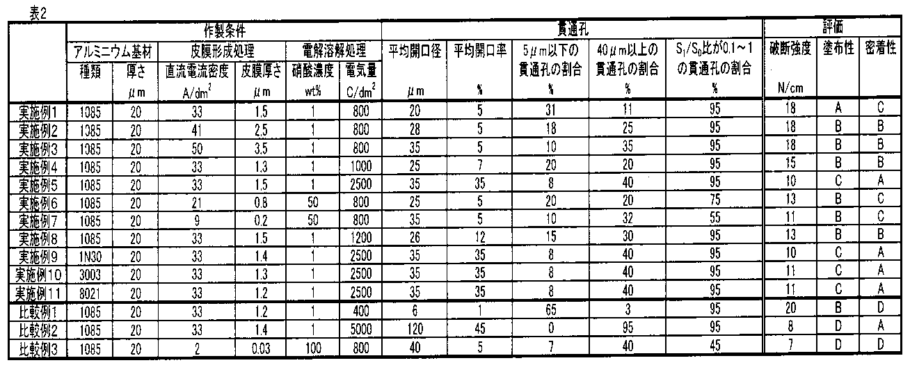
また、実施例2、6、7の対比等から、S1/S0比が0.1以上1以下の貫通孔の割合が大きいほど破断強度が高くなり、70%以上が好ましく、90%以上がより好ましいことがわかる。
また、実施例2、4、5、8等の対比から、平均開口率が小さいほど破断強度が高くなり、30%以下であるのが好ましいことがわかる。
また、実施例1~5等の対比から、開口径が5μm以下の貫通孔の割合が少ないほど密着性が向上し、30%以下であるのが好ましく、また、開口径が40μm以上の貫通孔の割合が少ないほど塗布性が向上し、30%以下であるのが好ましいことがわかる。
以上より本発明の効果は明らかである。
2 水酸化アルミニウム皮膜
3 貫通孔を有するアルミニウム基材
4 貫通孔を有する水酸化アルミニウム皮膜
5 貫通孔
6 第1の金属層
7 第2の金属層
10 アルミニウム板
30 電極
32 活物質層
Claims (12)
- 厚み方向に貫通する複数の貫通孔を有するアルミニウム板であって、
前記複数の貫通孔の平均開口径が0.1μm以上100μm以下であり、
前記複数の貫通孔の平均開口率が2%以上40%以下であり、
前記複数の貫通孔のうち、開口径が5μm以下の貫通孔の割合が40%以下であり、
前記複数の貫通孔のうち、開口径が40μm以上の貫通孔の割合が40%以下であり、
前記複数の貫通孔のうち、前記貫通孔の面積S1と、前記貫通孔の長軸を直径とした円の面積S0との比S1/S0が、0.1以上1以下である貫通孔の割合が50%以上であることを特徴とするアルミニウム板。 - 前記複数の貫通孔のうち、前記貫通孔の面積S1と、前記貫通孔の長軸を直径とした円の面積S0との比S1/S0が、0.1以上1以下である貫通孔の割合が70%以上である請求項1に記載のアルミニウム板。
- 前記複数の貫通孔のうち、開口径が5μm以下の貫通孔の割合が30%以下である請求項1または2に記載のアルミニウム板。
- 前記複数の貫通孔のうち、開口径が40μm以上の貫通孔の割合が30%以下である請求項1~3のいずれか一項に記載のアルミニウム板。
- 前記複数の貫通孔の平均開口径が0.1μm以上50μm以下である請求項1~4のいずれか一項に記載のアルミニウム板。
- 前記複数の貫通孔のうち、開口径が30μm以上の貫通孔の割合が30%以下である請求項1~5のいずれか一項に記載のアルミニウム板。
- 厚みが5~1000μmである請求項1~6のいずれか一項に記載のアルミニウム板。
- 前記複数の貫通孔の平均開口率が30%以下である請求項1~7のいずれか一項に記載のアルミニウム板。
- 隣接する前記貫通孔の孔間距離の最大値が300μm以下である請求項1~8のいずれか一項に記載のアルミニウム板。
- 厚み方向に複数の貫通孔を有するアルミニウム板の製造方法であって、
アルミニウム基材の表面に水酸化アルミニウムまたは酸化アルミニウムを主成分とする皮膜を形成する皮膜形成工程と、
前記皮膜形成工程の後に、電解溶解処理を施し、前記貫通孔を形成する貫通孔形成工程と、
前記貫通孔形成工程の後に、前記皮膜を除去する皮膜除去工程とを有し、
前記皮膜形成工程は、酸を用いて電気化学的処理を行って、前記皮膜を形成するものであり、電気化学的処理における電流密度が3A/dm2~60A/dm2であり、形成する前記皮膜の厚さが0.05μm以上100μm以下であることを特徴とするアルミニウム板の製造方法。 - 前記皮膜が水酸化アルミニウムを主成分とする皮膜である請求項10に記載のアルミニウム板の製造方法。
- 前記皮膜形成工程は、硝酸、塩酸、硫酸、燐酸、シュウ酸、あるいは、これらの2以上の混酸を用いて電気化学的処理を行って、前記皮膜を形成する請求項10または11に記載のアルミニウム板の製造方法。
Priority Applications (5)
| Application Number | Priority Date | Filing Date | Title |
|---|---|---|---|
| CN201680043645.0A CN107849725A (zh) | 2015-07-30 | 2016-07-27 | 铝板及铝板的制造方法 |
| KR1020187002789A KR20180025909A (ko) | 2015-07-30 | 2016-07-27 | 알루미늄판 및 알루미늄판의 제조 방법 |
| EP16830567.0A EP3330412A4 (en) | 2015-07-30 | 2016-07-27 | Aluminum plate and method for producing aluminum plate |
| JP2017530909A JPWO2017018462A1 (ja) | 2015-07-30 | 2016-07-27 | アルミニウム板 |
| US15/879,996 US20180166690A1 (en) | 2015-07-30 | 2018-01-25 | Aluminum plate and method for manufacturing aluminum plate |
Applications Claiming Priority (4)
| Application Number | Priority Date | Filing Date | Title |
|---|---|---|---|
| JP2015150312 | 2015-07-30 | ||
| JP2015-150312 | 2015-07-30 | ||
| JP2016087974 | 2016-04-26 | ||
| JP2016-087974 | 2016-04-26 |
Related Child Applications (1)
| Application Number | Title | Priority Date | Filing Date |
|---|---|---|---|
| US15/879,996 Continuation US20180166690A1 (en) | 2015-07-30 | 2018-01-25 | Aluminum plate and method for manufacturing aluminum plate |
Publications (1)
| Publication Number | Publication Date |
|---|---|
| WO2017018462A1 true WO2017018462A1 (ja) | 2017-02-02 |
Family
ID=57885606
Family Applications (1)
| Application Number | Title | Priority Date | Filing Date |
|---|---|---|---|
| PCT/JP2016/072070 WO2017018462A1 (ja) | 2015-07-30 | 2016-07-27 | アルミニウム板およびアルミニウム板の製造方法 |
Country Status (6)
| Country | Link |
|---|---|
| US (1) | US20180166690A1 (ja) |
| EP (1) | EP3330412A4 (ja) |
| JP (1) | JPWO2017018462A1 (ja) |
| KR (1) | KR20180025909A (ja) |
| CN (1) | CN107849725A (ja) |
| WO (1) | WO2017018462A1 (ja) |
Cited By (5)
| Publication number | Priority date | Publication date | Assignee | Title |
|---|---|---|---|---|
| WO2018235488A1 (ja) * | 2017-06-21 | 2018-12-27 | 富士フイルム株式会社 | 複合体 |
| WO2019026974A1 (ja) * | 2017-08-01 | 2019-02-07 | 日立化成株式会社 | アルミニウム箔、及び蓄電デバイス |
| CN110637385A (zh) * | 2017-05-18 | 2019-12-31 | 富士胶片株式会社 | 穿孔金属箔、穿孔金属箔的制造方法、二次电池用负极及二次电池用正极 |
| WO2020116004A1 (ja) * | 2018-12-05 | 2020-06-11 | 昭和電工株式会社 | リチウムイオン二次電池 |
| KR20210133270A (ko) | 2019-03-29 | 2021-11-05 | 후지필름 가부시키가이샤 | 알루미늄박, 알루미늄박의 제조 방법, 집전체, 리튬 이온 커패시터, 및, 리튬 이온 배터리 |
Families Citing this family (1)
| Publication number | Priority date | Publication date | Assignee | Title |
|---|---|---|---|---|
| JP6936864B2 (ja) * | 2017-10-16 | 2021-09-22 | 富士フイルム株式会社 | アルミニウム箔および電極用アルミニウム部材 |
Citations (6)
| Publication number | Priority date | Publication date | Assignee | Title |
|---|---|---|---|---|
| JP2005129924A (ja) * | 2003-10-02 | 2005-05-19 | Showa Denko Kk | 電気二重層コンデンサ用金属製集電体およびそれを用いた分極性電極並びに電気二重層コンデンサ |
| JP2009138229A (ja) * | 2007-12-06 | 2009-06-25 | Ulvac Japan Ltd | 保護膜製造方法 |
| JP2011216364A (ja) * | 2010-03-31 | 2011-10-27 | Toyo Aluminium Kk | 負極集電体用金属箔 |
| JP2011222672A (ja) * | 2010-04-07 | 2011-11-04 | Daiso Co Ltd | 孔あき導電箔及びその製造方法 |
| JP2011249150A (ja) * | 2010-05-27 | 2011-12-08 | Mitsubishi Alum Co Ltd | 蓄電デバイス集電体用アルミニウム箔及び蓄電デバイス集電体 |
| JP2014072267A (ja) * | 2012-09-28 | 2014-04-21 | Hitachi Aic Inc | 貫通孔を有するアルミニウム集電箔およびその製造方法 |
Family Cites Families (12)
| Publication number | Priority date | Publication date | Assignee | Title |
|---|---|---|---|---|
| JP4813152B2 (ja) * | 2005-11-14 | 2011-11-09 | 富士重工業株式会社 | リチウムイオンキャパシタ |
| JP5363818B2 (ja) * | 2006-12-27 | 2013-12-11 | Jmエナジー株式会社 | 塗布電極及び有機電解質キャパシタ |
| CN103119774B (zh) * | 2010-09-22 | 2016-01-20 | 丰田自动车株式会社 | 非水电解质二次电池 |
| WO2013018157A1 (ja) * | 2011-07-29 | 2013-02-07 | 古河スカイ株式会社 | 集電体、電極構造体、非水電解質電池、蓄電部品 |
| JP2013058613A (ja) * | 2011-09-08 | 2013-03-28 | Nec Tokin Corp | 蓄電デバイス |
| JP6066299B2 (ja) * | 2013-02-14 | 2017-01-25 | 日本軽金属株式会社 | アルミニウム製熱交換器 |
| CN103384012A (zh) * | 2013-06-26 | 2013-11-06 | 东莞新能源科技有限公司 | 锂离子电池正极集流体结构及包含该结构的电池 |
| CN103531816B (zh) * | 2013-09-26 | 2015-11-25 | 惠州市惠德瑞锂电科技有限公司 | 一种含软态铝箔的锂一次电池 |
| JP2015109214A (ja) * | 2013-12-05 | 2015-06-11 | 株式会社豊田自動織機 | 集電体およびリチウムイオン二次電池 |
| CN104282917A (zh) * | 2014-09-24 | 2015-01-14 | 襄阳锦翔光电科技股份有限公司 | 一种锂离子电池正极集流体 |
| KR101915483B1 (ko) * | 2014-09-30 | 2018-11-06 | 후지필름 가부시키가이샤 | 알루미늄판 |
| JP2015213180A (ja) * | 2015-06-16 | 2015-11-26 | 東洋アルミニウム株式会社 | 負極集電体用金属箔 |
-
2016
- 2016-07-27 EP EP16830567.0A patent/EP3330412A4/en not_active Withdrawn
- 2016-07-27 CN CN201680043645.0A patent/CN107849725A/zh active Pending
- 2016-07-27 JP JP2017530909A patent/JPWO2017018462A1/ja active Pending
- 2016-07-27 WO PCT/JP2016/072070 patent/WO2017018462A1/ja active Application Filing
- 2016-07-27 KR KR1020187002789A patent/KR20180025909A/ko not_active Application Discontinuation
-
2018
- 2018-01-25 US US15/879,996 patent/US20180166690A1/en not_active Abandoned
Patent Citations (6)
| Publication number | Priority date | Publication date | Assignee | Title |
|---|---|---|---|---|
| JP2005129924A (ja) * | 2003-10-02 | 2005-05-19 | Showa Denko Kk | 電気二重層コンデンサ用金属製集電体およびそれを用いた分極性電極並びに電気二重層コンデンサ |
| JP2009138229A (ja) * | 2007-12-06 | 2009-06-25 | Ulvac Japan Ltd | 保護膜製造方法 |
| JP2011216364A (ja) * | 2010-03-31 | 2011-10-27 | Toyo Aluminium Kk | 負極集電体用金属箔 |
| JP2011222672A (ja) * | 2010-04-07 | 2011-11-04 | Daiso Co Ltd | 孔あき導電箔及びその製造方法 |
| JP2011249150A (ja) * | 2010-05-27 | 2011-12-08 | Mitsubishi Alum Co Ltd | 蓄電デバイス集電体用アルミニウム箔及び蓄電デバイス集電体 |
| JP2014072267A (ja) * | 2012-09-28 | 2014-04-21 | Hitachi Aic Inc | 貫通孔を有するアルミニウム集電箔およびその製造方法 |
Non-Patent Citations (1)
| Title |
|---|
| See also references of EP3330412A4 * |
Cited By (8)
| Publication number | Priority date | Publication date | Assignee | Title |
|---|---|---|---|---|
| CN110637385A (zh) * | 2017-05-18 | 2019-12-31 | 富士胶片株式会社 | 穿孔金属箔、穿孔金属箔的制造方法、二次电池用负极及二次电池用正极 |
| EP3627599A4 (en) * | 2017-05-18 | 2020-05-27 | FUJIFILM Corporation | PERFORATED METAL FILM, METHOD FOR PRODUCING THE PERFORATED METAL FILM, NEGATIVE SECONDARY BATTERY ELECTRODE AND POSITIVE SECONDARY BATTERY ELECTRODE |
| WO2018235488A1 (ja) * | 2017-06-21 | 2018-12-27 | 富士フイルム株式会社 | 複合体 |
| JPWO2018235488A1 (ja) * | 2017-06-21 | 2020-04-02 | 富士フイルム株式会社 | 複合体 |
| EP3643497A4 (en) * | 2017-06-21 | 2020-04-29 | Fujifilm Corporation | COMPOSITE BODY |
| WO2019026974A1 (ja) * | 2017-08-01 | 2019-02-07 | 日立化成株式会社 | アルミニウム箔、及び蓄電デバイス |
| WO2020116004A1 (ja) * | 2018-12-05 | 2020-06-11 | 昭和電工株式会社 | リチウムイオン二次電池 |
| KR20210133270A (ko) | 2019-03-29 | 2021-11-05 | 후지필름 가부시키가이샤 | 알루미늄박, 알루미늄박의 제조 방법, 집전체, 리튬 이온 커패시터, 및, 리튬 이온 배터리 |
Also Published As
| Publication number | Publication date |
|---|---|
| EP3330412A4 (en) | 2018-07-18 |
| CN107849725A (zh) | 2018-03-27 |
| EP3330412A1 (en) | 2018-06-06 |
| US20180166690A1 (en) | 2018-06-14 |
| KR20180025909A (ko) | 2018-03-09 |
| JPWO2017018462A1 (ja) | 2018-06-28 |
Similar Documents
| Publication | Publication Date | Title |
|---|---|---|
| WO2017018462A1 (ja) | アルミニウム板およびアルミニウム板の製造方法 | |
| JP6374013B2 (ja) | アルミニウム板 | |
| JP6328785B2 (ja) | アルミニウム板およびアルミニウム板の製造方法 | |
| JP6199416B2 (ja) | アルミニウム板の製造方法、アルミニウム板、蓄電デバイス用集電体、蓄電デバイス、防音・吸音材、電磁波シールドおよび建築用材料 | |
| WO2016017380A1 (ja) | アルミニウム板 | |
| JP6636612B2 (ja) | アルミニウム板の製造方法、及び、アルミニウム板の製造装置 | |
| US11527760B2 (en) | Aluminum member for electrodes and method of producing aluminum member for electrodes | |
| JP6936864B2 (ja) | アルミニウム箔および電極用アルミニウム部材 |
Legal Events
| Date | Code | Title | Description |
|---|---|---|---|
| 121 | Ep: the epo has been informed by wipo that ep was designated in this application |
Ref document number: 16830567 Country of ref document: EP Kind code of ref document: A1 |
|
| ENP | Entry into the national phase |
Ref document number: 2017530909 Country of ref document: JP Kind code of ref document: A |
|
| ENP | Entry into the national phase |
Ref document number: 20187002789 Country of ref document: KR Kind code of ref document: A |
|
| NENP | Non-entry into the national phase |
Ref country code: DE |
|
| WWE | Wipo information: entry into national phase |
Ref document number: 2016830567 Country of ref document: EP |