WO2017018141A1 - エピタキシャルシリコンウェーハ - Google Patents
エピタキシャルシリコンウェーハ Download PDFInfo
- Publication number
- WO2017018141A1 WO2017018141A1 PCT/JP2016/069980 JP2016069980W WO2017018141A1 WO 2017018141 A1 WO2017018141 A1 WO 2017018141A1 JP 2016069980 W JP2016069980 W JP 2016069980W WO 2017018141 A1 WO2017018141 A1 WO 2017018141A1
- Authority
- WO
- WIPO (PCT)
- Prior art keywords
- boron
- silicon substrate
- oxygen
- atoms
- concentration
- Prior art date
- Legal status (The legal status is an assumption and is not a legal conclusion. Google has not performed a legal analysis and makes no representation as to the accuracy of the status listed.)
- Ceased
Links
Images


Classifications
-
- H—ELECTRICITY
- H10—SEMICONDUCTOR DEVICES; ELECTRIC SOLID-STATE DEVICES NOT OTHERWISE PROVIDED FOR
- H10P—GENERIC PROCESSES OR APPARATUS FOR THE MANUFACTURE OR TREATMENT OF DEVICES COVERED BY CLASS H10
- H10P14/00—Formation of materials, e.g. in the shape of layers or pillars
- H10P14/60—Formation of materials, e.g. in the shape of layers or pillars of insulating materials
- H10P14/63—Formation of materials, e.g. in the shape of layers or pillars of insulating materials characterised by the formation processes
- H10P14/6326—Deposition processes
- H10P14/6349—Deposition of epitaxial materials
-
- H—ELECTRICITY
- H10—SEMICONDUCTOR DEVICES; ELECTRIC SOLID-STATE DEVICES NOT OTHERWISE PROVIDED FOR
- H10F—INORGANIC SEMICONDUCTOR DEVICES SENSITIVE TO INFRARED RADIATION, LIGHT, ELECTROMAGNETIC RADIATION OF SHORTER WAVELENGTH OR CORPUSCULAR RADIATION
- H10F77/00—Constructional details of devices covered by this subclass
- H10F77/10—Semiconductor bodies
- H10F77/12—Active materials
- H10F77/122—Active materials comprising only Group IV materials
- H10F77/1223—Active materials comprising only Group IV materials characterised by the dopants
-
- C—CHEMISTRY; METALLURGY
- C30—CRYSTAL GROWTH
- C30B—SINGLE-CRYSTAL GROWTH; UNIDIRECTIONAL SOLIDIFICATION OF EUTECTIC MATERIAL OR UNIDIRECTIONAL DEMIXING OF EUTECTOID MATERIAL; REFINING BY ZONE-MELTING OF MATERIAL; PRODUCTION OF A HOMOGENEOUS POLYCRYSTALLINE MATERIAL WITH DEFINED STRUCTURE; SINGLE CRYSTALS OR HOMOGENEOUS POLYCRYSTALLINE MATERIAL WITH DEFINED STRUCTURE; AFTER-TREATMENT OF SINGLE CRYSTALS OR A HOMOGENEOUS POLYCRYSTALLINE MATERIAL WITH DEFINED STRUCTURE; APPARATUS THEREFOR
- C30B15/00—Single-crystal growth by pulling from a melt, e.g. Czochralski method
- C30B15/20—Controlling or regulating
- C30B15/203—Controlling or regulating the relationship of pull rate (v) to axial thermal gradient (G)
-
- C—CHEMISTRY; METALLURGY
- C30—CRYSTAL GROWTH
- C30B—SINGLE-CRYSTAL GROWTH; UNIDIRECTIONAL SOLIDIFICATION OF EUTECTIC MATERIAL OR UNIDIRECTIONAL DEMIXING OF EUTECTOID MATERIAL; REFINING BY ZONE-MELTING OF MATERIAL; PRODUCTION OF A HOMOGENEOUS POLYCRYSTALLINE MATERIAL WITH DEFINED STRUCTURE; SINGLE CRYSTALS OR HOMOGENEOUS POLYCRYSTALLINE MATERIAL WITH DEFINED STRUCTURE; AFTER-TREATMENT OF SINGLE CRYSTALS OR A HOMOGENEOUS POLYCRYSTALLINE MATERIAL WITH DEFINED STRUCTURE; APPARATUS THEREFOR
- C30B15/00—Single-crystal growth by pulling from a melt, e.g. Czochralski method
- C30B15/30—Mechanisms for rotating or moving either the melt or the crystal
- C30B15/305—Stirring of the melt
-
- C—CHEMISTRY; METALLURGY
- C30—CRYSTAL GROWTH
- C30B—SINGLE-CRYSTAL GROWTH; UNIDIRECTIONAL SOLIDIFICATION OF EUTECTIC MATERIAL OR UNIDIRECTIONAL DEMIXING OF EUTECTOID MATERIAL; REFINING BY ZONE-MELTING OF MATERIAL; PRODUCTION OF A HOMOGENEOUS POLYCRYSTALLINE MATERIAL WITH DEFINED STRUCTURE; SINGLE CRYSTALS OR HOMOGENEOUS POLYCRYSTALLINE MATERIAL WITH DEFINED STRUCTURE; AFTER-TREATMENT OF SINGLE CRYSTALS OR A HOMOGENEOUS POLYCRYSTALLINE MATERIAL WITH DEFINED STRUCTURE; APPARATUS THEREFOR
- C30B25/00—Single-crystal growth by chemical reaction of reactive gases, e.g. chemical vapour-deposition growth
- C30B25/02—Epitaxial-layer growth
- C30B25/18—Epitaxial-layer growth characterised by the substrate
-
- C—CHEMISTRY; METALLURGY
- C30—CRYSTAL GROWTH
- C30B—SINGLE-CRYSTAL GROWTH; UNIDIRECTIONAL SOLIDIFICATION OF EUTECTIC MATERIAL OR UNIDIRECTIONAL DEMIXING OF EUTECTOID MATERIAL; REFINING BY ZONE-MELTING OF MATERIAL; PRODUCTION OF A HOMOGENEOUS POLYCRYSTALLINE MATERIAL WITH DEFINED STRUCTURE; SINGLE CRYSTALS OR HOMOGENEOUS POLYCRYSTALLINE MATERIAL WITH DEFINED STRUCTURE; AFTER-TREATMENT OF SINGLE CRYSTALS OR A HOMOGENEOUS POLYCRYSTALLINE MATERIAL WITH DEFINED STRUCTURE; APPARATUS THEREFOR
- C30B29/00—Single crystals or homogeneous polycrystalline material with defined structure characterised by the material or by their shape
- C30B29/02—Elements
- C30B29/06—Silicon
-
- C—CHEMISTRY; METALLURGY
- C30—CRYSTAL GROWTH
- C30B—SINGLE-CRYSTAL GROWTH; UNIDIRECTIONAL SOLIDIFICATION OF EUTECTIC MATERIAL OR UNIDIRECTIONAL DEMIXING OF EUTECTOID MATERIAL; REFINING BY ZONE-MELTING OF MATERIAL; PRODUCTION OF A HOMOGENEOUS POLYCRYSTALLINE MATERIAL WITH DEFINED STRUCTURE; SINGLE CRYSTALS OR HOMOGENEOUS POLYCRYSTALLINE MATERIAL WITH DEFINED STRUCTURE; AFTER-TREATMENT OF SINGLE CRYSTALS OR A HOMOGENEOUS POLYCRYSTALLINE MATERIAL WITH DEFINED STRUCTURE; APPARATUS THEREFOR
- C30B30/00—Production of single crystals or homogeneous polycrystalline material with defined structure characterised by the action of electric or magnetic fields, wave energy or other specific physical conditions
- C30B30/04—Production of single crystals or homogeneous polycrystalline material with defined structure characterised by the action of electric or magnetic fields, wave energy or other specific physical conditions using magnetic fields
-
- C—CHEMISTRY; METALLURGY
- C30—CRYSTAL GROWTH
- C30B—SINGLE-CRYSTAL GROWTH; UNIDIRECTIONAL SOLIDIFICATION OF EUTECTIC MATERIAL OR UNIDIRECTIONAL DEMIXING OF EUTECTOID MATERIAL; REFINING BY ZONE-MELTING OF MATERIAL; PRODUCTION OF A HOMOGENEOUS POLYCRYSTALLINE MATERIAL WITH DEFINED STRUCTURE; SINGLE CRYSTALS OR HOMOGENEOUS POLYCRYSTALLINE MATERIAL WITH DEFINED STRUCTURE; AFTER-TREATMENT OF SINGLE CRYSTALS OR A HOMOGENEOUS POLYCRYSTALLINE MATERIAL WITH DEFINED STRUCTURE; APPARATUS THEREFOR
- C30B33/00—After-treatment of single crystals or homogeneous polycrystalline material with defined structure
- C30B33/02—Heat treatment
-
- H—ELECTRICITY
- H10—SEMICONDUCTOR DEVICES; ELECTRIC SOLID-STATE DEVICES NOT OTHERWISE PROVIDED FOR
- H10F—INORGANIC SEMICONDUCTOR DEVICES SENSITIVE TO INFRARED RADIATION, LIGHT, ELECTROMAGNETIC RADIATION OF SHORTER WAVELENGTH OR CORPUSCULAR RADIATION
- H10F39/00—Integrated devices, or assemblies of multiple devices, comprising at least one element covered by group H10F30/00, e.g. radiation detectors comprising photodiode arrays
- H10F39/011—Manufacture or treatment of image sensors covered by group H10F39/12
- H10F39/026—Wafer-level processing
-
- H—ELECTRICITY
- H10—SEMICONDUCTOR DEVICES; ELECTRIC SOLID-STATE DEVICES NOT OTHERWISE PROVIDED FOR
- H10P—GENERIC PROCESSES OR APPARATUS FOR THE MANUFACTURE OR TREATMENT OF DEVICES COVERED BY CLASS H10
- H10P14/00—Formation of materials, e.g. in the shape of layers or pillars
- H10P14/60—Formation of materials, e.g. in the shape of layers or pillars of insulating materials
- H10P14/69—Inorganic materials
- H10P14/692—Inorganic materials composed of oxides, glassy oxides or oxide-based glasses
- H10P14/6921—Inorganic materials composed of oxides, glassy oxides or oxide-based glasses containing silicon
- H10P14/6922—Inorganic materials composed of oxides, glassy oxides or oxide-based glasses containing silicon the material containing Si, O and at least one of H, N, C, F or other non-metal elements, e.g. SiOC, SiOC:H or SiONC
- H10P14/6923—Inorganic materials composed of oxides, glassy oxides or oxide-based glasses containing silicon the material containing Si, O and at least one of H, N, C, F or other non-metal elements, e.g. SiOC, SiOC:H or SiONC the material being boron or phosphorus doped silicon oxides, e.g. BPSG, BSG or PSG
-
- H—ELECTRICITY
- H10—SEMICONDUCTOR DEVICES; ELECTRIC SOLID-STATE DEVICES NOT OTHERWISE PROVIDED FOR
- H10P—GENERIC PROCESSES OR APPARATUS FOR THE MANUFACTURE OR TREATMENT OF DEVICES COVERED BY CLASS H10
- H10P36/00—Gettering within semiconductor bodies
- H10P36/20—Intrinsic gettering, i.e. thermally inducing defects by using oxygen present in the silicon body
-
- H—ELECTRICITY
- H10—SEMICONDUCTOR DEVICES; ELECTRIC SOLID-STATE DEVICES NOT OTHERWISE PROVIDED FOR
- H10P—GENERIC PROCESSES OR APPARATUS FOR THE MANUFACTURE OR TREATMENT OF DEVICES COVERED BY CLASS H10
- H10P95/00—Generic processes or apparatus for manufacture or treatments not covered by the other groups of this subclass
- H10P95/90—Thermal treatments, e.g. annealing or sintering
-
- H—ELECTRICITY
- H10—SEMICONDUCTOR DEVICES; ELECTRIC SOLID-STATE DEVICES NOT OTHERWISE PROVIDED FOR
- H10P—GENERIC PROCESSES OR APPARATUS FOR THE MANUFACTURE OR TREATMENT OF DEVICES COVERED BY CLASS H10
- H10P14/00—Formation of materials, e.g. in the shape of layers or pillars
- H10P14/20—Formation of materials, e.g. in the shape of layers or pillars of semiconductor materials
- H10P14/24—Formation of materials, e.g. in the shape of layers or pillars of semiconductor materials using chemical vapour deposition [CVD]
-
- H—ELECTRICITY
- H10—SEMICONDUCTOR DEVICES; ELECTRIC SOLID-STATE DEVICES NOT OTHERWISE PROVIDED FOR
- H10P—GENERIC PROCESSES OR APPARATUS FOR THE MANUFACTURE OR TREATMENT OF DEVICES COVERED BY CLASS H10
- H10P14/00—Formation of materials, e.g. in the shape of layers or pillars
- H10P14/20—Formation of materials, e.g. in the shape of layers or pillars of semiconductor materials
- H10P14/29—Formation of materials, e.g. in the shape of layers or pillars of semiconductor materials characterised by the substrates
- H10P14/2901—Materials
- H10P14/2902—Materials being Group IVA materials
- H10P14/2905—Silicon, silicon germanium or germanium
-
- H—ELECTRICITY
- H10—SEMICONDUCTOR DEVICES; ELECTRIC SOLID-STATE DEVICES NOT OTHERWISE PROVIDED FOR
- H10P—GENERIC PROCESSES OR APPARATUS FOR THE MANUFACTURE OR TREATMENT OF DEVICES COVERED BY CLASS H10
- H10P14/00—Formation of materials, e.g. in the shape of layers or pillars
- H10P14/20—Formation of materials, e.g. in the shape of layers or pillars of semiconductor materials
- H10P14/34—Deposited materials, e.g. layers
- H10P14/3402—Deposited materials, e.g. layers characterised by the chemical composition
- H10P14/3404—Deposited materials, e.g. layers characterised by the chemical composition being Group IVA materials
- H10P14/3411—Silicon, silicon germanium or germanium
-
- H—ELECTRICITY
- H10—SEMICONDUCTOR DEVICES; ELECTRIC SOLID-STATE DEVICES NOT OTHERWISE PROVIDED FOR
- H10P—GENERIC PROCESSES OR APPARATUS FOR THE MANUFACTURE OR TREATMENT OF DEVICES COVERED BY CLASS H10
- H10P14/00—Formation of materials, e.g. in the shape of layers or pillars
- H10P14/20—Formation of materials, e.g. in the shape of layers or pillars of semiconductor materials
- H10P14/38—Formation of materials, e.g. in the shape of layers or pillars of semiconductor materials characterised by treatments done after the formation of the materials
Definitions
- the present invention relates to an epitaxial silicon wafer, and particularly to an epitaxial silicon wafer in which an epitaxial layer is formed on the surface of a p-type silicon substrate doped with boron.
- Epitaxial silicon wafers are widely used as substrate materials for semiconductor devices.
- An epitaxial silicon wafer is obtained by forming an epitaxial layer on the surface of a bulk silicon substrate and has high crystal perfection. Therefore, it is possible to manufacture a semiconductor device with high quality and high reliability.
- Patent Document 1 includes a wafer having a nitrogen concentration of 1 ⁇ 10 12 atoms / cm 3 or more, or a specific resistance set to 20 m ⁇ ⁇ cm or less by boron doping, and an epitaxial layer provided on the wafer surface.
- An epitaxial silicon wafer is described in which the initial oxygen concentration of the wafer is 14 ⁇ 10 17 atoms / cm 3 or less.
- Patent Document 2 discloses that a p-type silicon substrate to which carbon and nitrogen are added and has a resistivity of less than 100 ⁇ ⁇ cm, a p-type first epitaxial layer on the p-type silicon substrate, and a p-type first epitaxial layer
- An interstitial oxygen concentration in the p-type silicon substrate is 10 ⁇ 10 17 to 20 ⁇ 10 17 atoms / cm 3
- An epitaxial wafer for backside illumination type solid-state imaging device is described in which the density of precipitates in the central portion in the direction is 5 ⁇ 10 5 / cm 2 or more and 5 ⁇ 10 7 / cm 2 or less. According to this epitaxial wafer, it is possible to manufacture a back-illuminated solid-state imaging device with a higher yield.
- boron in a silicon substrate is indispensable for ensuring gettering capability and reducing the resistance of the substrate.
- the impurity profile of the epitaxial layer changes and the uniformity of resistivity in the wafer surface deteriorates.
- the width of the boron concentration transition region (resistance variable layer) in the epitaxial layer near the boundary with the silicon substrate is widened, the effective thickness of the epitaxial layer is reduced, and the characteristics of the semiconductor device may be deteriorated. Therefore, it is necessary to suppress the diffusion of boron in the silicon substrate as much as possible.
- boron in a silicon substrate diffuses at a high speed by heat treatment in an oxidizing atmosphere.
- Si atoms that occupy space by SiO 2 and have lost their place are pushed out of the crystal lattice, and the interstitial silicon increases.
- boron is kicked out and diffused while being replaced with interstitial silicon, boron is diffused at an increased rate due to an increase in interstitial silicon. Therefore, one method for suppressing the accelerated diffusion of boron is to not perform the heat treatment step in an oxidizing atmosphere as much as possible.
- the present invention has been made in view of the above problems, and an object thereof is to provide an epitaxial silicon wafer in which accelerated diffusion of boron in a silicon substrate is suppressed.
- the inventors of the present application are not limited to heat treatment in an oxidizing atmosphere, but also when oxygen precipitates in a silicon substrate grow by arbitrary heat treatment. It was revealed that interstitial silicon was released and boron kickout diffusion was promoted through the interstitial silicon.
- the present invention has been achieved by paying attention to the fact that boron diffusion caused by oxygen precipitates progresses rapidly when the oxygen precipitate density in the silicon substrate exceeds a certain threshold level.
- an epitaxial silicon wafer according to the present invention is an epitaxial silicon wafer in which an epitaxial layer is formed on the surface of a silicon substrate doped with boron, and the silicon substrate includes
- the boron concentration of the silicon substrate is not less than 2.7 ⁇ 10 17 atoms / cm 3 and not more than 1.3 ⁇ 10 19 atoms / cm 3
- the initial oxygen concentration in the silicon substrate is not more than 11 ⁇ 10 17 atoms / cm 3
- the oxygen precipitate density in the silicon substrate is 1 ⁇ 10 10 pieces / cm 3 or less.
- the oxygen precipitate density in the silicon substrate is 1 ⁇ 10 10 pieces / cm 3 or less.
- the interstitial silicon increases, and it is possible to suppress the kickout diffusion of boron in the silicon substrate to the epitaxial layer side through the interstitial silicon, and the oxygen precipitate density is substantially reduced.
- the diffusion level can be suppressed to the same level as in the case of zero.
- the boron concentration in the silicon substrate is preferably 2.7 ⁇ 10 17 atoms / cm 3 or more and 1.3 ⁇ 10 19 atoms / cm 3 or less
- the initial oxygen concentration in the silicon substrate is It is preferably 11 ⁇ 10 17 atoms / cm 3 or less. If the initial oxygen concentration in the silicon substrate is 11 ⁇ 10 17 atoms / cm 3 or less, even if the oxygen precipitates in the silicon substrate grow by an arbitrary heat treatment in the device process, the oxygen precipitate density in the silicon substrate is 1 ⁇ 10 10 pieces / cm 3 or less can be suppressed.
- the boron concentration Y (atoms / cm 3) and the initial oxygen concentration X ( ⁇ 10 17 atoms / cm 3) is to satisfy a relational expression X ⁇ -4.3 ⁇ 10 -19 Y + 16.3 Is preferred.
- the oxygen precipitate density can be suppressed to 1 ⁇ 10 10 atoms / cm 3 or less regardless of the boron concentration in the silicon substrate. Therefore, accelerated diffusion of boron due to oxygen precipitates can be suppressed.
- an epitaxial silicon wafer capable of suppressing the accelerated diffusion of boron in the silicon substrate even when oxygen precipitates are grown by an arbitrary heat treatment in the device process.
- FIG. 1 is a schematic cross-sectional view showing the structure of an epitaxial silicon wafer according to an embodiment of the present invention.
- the epitaxial silicon wafer 10 includes a silicon substrate 11 and an epitaxial layer 12 formed on the surface of the silicon substrate 11.
- the silicon substrate 11 is a polished wafer that is cut out from a silicon single crystal ingot grown by the Czochralski method (CZ method) and mirror-polished on the surface.
- the silicon substrate 11 serves as a gettering sink for securing the mechanical strength of the epitaxial silicon wafer 10 and capturing heavy metals.
- the thickness of the silicon substrate 11 is not particularly limited as long as the mechanical strength can be ensured, but may be, for example, 725 mm.
- the silicon substrate 11 is a p-type silicon substrate doped with boron.
- the boron concentration in the silicon substrate 11 is preferably 2.7 ⁇ 10 17 atoms / cm 3 or more and 1.3 ⁇ 10 19 atoms / cm 3 or less, and the specific resistance of the silicon substrate 11 is 20 m ⁇ ⁇ cm or less. It is preferable.
- the silicon substrate 11 doped with boron at a high concentration the resistance of the silicon substrate 11 can be reduced, and sufficient gettering ability can be secured.
- An epitaxial layer 12 is formed on the surface of the silicon substrate 11, and a semiconductor device such as a MOS transistor is formed on the epitaxial layer 12.
- the thickness of the epitaxial layer 12 is preferably 1 to 10 ⁇ m.
- the epitaxial layer 12 may have a multilayer structure in which a plurality of epitaxial layers having different characteristics are stacked. Usually, the specific resistance of the epitaxial layer 12 is set higher than that of the silicon substrate 11, and a p-type dopant (boron) or an n-type dopant (phosphorus, arsenic, antimony) is added.
- the oxygen precipitate density in the silicon substrate 11 is 1 ⁇ 10 10 pieces / cm 3 or less.
- the oxygen precipitate density is 1 ⁇ 10 10 pieces / cm 3 or less, the influence of oxygen precipitates in the silicon substrate 11 on the diffusion of boron is very small, and the oxygen precipitate density is substantially reduced. Therefore, the diffusion level can be suppressed to the same level as that in the case of zero.
- the oxygen precipitate evaluation heat treatment is, for example, a two-step heat treatment in which a heat treatment at 700 ° C. for 3 hours (nucleation process) and a heat treatment at 1000 ° C. for 16 hours (nucleation growth process) are sequentially performed. It is. Since these heat treatments are performed not in an oxidizing atmosphere but in a nitrogen atmosphere, a thermal oxide film is not formed, and there is no problem of accelerated diffusion of boron due to the generation of the thermal oxide film. However, the growth of oxygen precipitation nuclei in the silicon substrate 11 increases the oxygen precipitate density, which becomes a new cause of boron diffusion.
- boron in the silicon substrate 11 has an action of promoting oxygen precipitation, and the density of oxygen precipitates in the silicon substrate increases as the boron concentration increases. Oxygen precipitates are necessary to some extent for securing the gettering ability, but boron diffuses at an increased rate as the amount of oxygen precipitation increases.
- the initial oxygen concentration between lattices of the silicon substrate 11 needs to be set to 11 ⁇ 10 17 atoms / cm 3 or less.
- the initial oxygen concentration is higher than 11 ⁇ 10 17 atoms / cm 3
- interstitial silicon increases with an increase in oxygen precipitate density, and boron diffuses at an accelerated rate through the interstitial silicon.
- the lower the initial oxygen concentration the better.
- the lower limit is not particularly limited, but at present, growing a silicon single crystal having an initial oxygen concentration lower than 1 ⁇ 10 17 atoms / cm 3 by the CZ method is a manufacturing process. It is difficult.
- the oxygen concentrations described in this specification are all measured by Fourier transform infrared spectrophotometry (FT-IR) standardized by ASTM F-121 (1979).
- a preferable range of the initial oxygen concentration in the silicon substrate 11 varies depending on the boron concentration.
- the boron concentration in the silicon substrate 11 is low, there is no problem even if the initial oxygen concentration is somewhat high. However, when the boron concentration is high, oxygen precipitation nuclei are likely to grow, and this occurs unless the initial oxygen concentration is low. This is because the oxygen precipitates are excessive and the oxygen precipitate density cannot be suppressed to 1 ⁇ 10 10 pieces / cm 3 or less.
- the initial oxygen concentration X ( ⁇ 10 17 atoms / cm 3 ) and the boron concentration Y (atoms / cm 3 ) in the silicon substrate 11 are set, they satisfy X ⁇ ⁇ 4.3 ⁇ 10 ⁇ 19 Y + 16.3. It is preferable to satisfy the relational expression. When this relational expression is satisfied, the oxygen precipitate density in the silicon substrate 11 can be suppressed to 1 ⁇ 10 10 pieces / cm 3 or less regardless of the boron concentration.
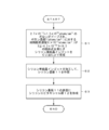
- FIG. 2 is a flowchart for explaining a method of manufacturing the epitaxial silicon wafer 10.
- a silicon single crystal ingot doped with boron is first grown by the CZ method (step S1). At this time, the silicon single crystal is doped with 2.7 ⁇ 10 17 to 1.3 ⁇ 10 19 atoms / cm 3 of boron.
- the silicon single crystal contains oxygen eluted from the quartz crucible in supersaturation, but the oxygen concentration in the silicon single crystal is controlled by controlling the pulling conditions. That is, as described above, the oxygen concentration X ( ⁇ 10 17 atoms / cm 3 ) and the boron concentration Y (atoms / cm 3 ) in the silicon single crystal satisfy the relationship of X ⁇ ⁇ 4.3 ⁇ 10 ⁇ 19 Y + 16.3. The pulling condition is controlled to satisfy the equation.
- Boron in the single crystal is added by filling a predetermined amount of boron together with the silicon raw material when the silicon raw material is charged into the quartz crucible. Boron is filled with a target resistivity at the top position of the single crystal, and boron is melted together with the silicon raw material to produce a silicon melt containing boron.
- the single crystal pulled from this silicon melt contains boron at a constant rate, but the boron concentration increases in the ingot pulling length direction as crystal growth proceeds due to segregation, so that the above relational expression is satisfied. It is necessary to reduce the oxygen concentration in the single crystal in the ingot pulling length direction.
- the oxygen concentration in the single crystal can be controlled by adjusting the rotation speed and heater power of the quartz crucible.
- the quartz crucible may be rotated at a low speed or the heater power may be set to a low output.
- the oxygen concentration in the single crystal can be kept low.
- the MCZ method of pulling up the single crystal while applying a magnetic field to the silicon melt is also very effective.
- the melt convection is suppressed by the influence of the magnetic field, so that the elution of oxygen from the quartz crucible to the silicon melt can be suppressed, and the oxygen concentration in the single crystal pulled from the silicon melt is kept low. Can do.
- the silicon single crystal ingot is processed to produce the silicon substrate 11 (step S2).
- the silicon substrate 11 is a polished wafer cut out from a silicon single crystal ingot and mirror-polished on the surface.
- the boron concentration of the silicon substrate 11 is 2.7 ⁇ 10 17 atoms / cm 3 or more and 1.3 ⁇ 10 19 atoms / cm 3 or less, and the initial oxygen concentration in the silicon substrate 11 is 11 ⁇ 10 17 atoms / cm 3. 3 or less.
- step S3 the epitaxial layer 12 is formed on the surface of the silicon substrate 11 by a known method.
- step S3 the epitaxial silicon wafer 10 is completed.
- the epitaxial silicon wafer 10 manufactured in this way is used as a substrate material for semiconductor devices, and becomes various semiconductor devices through various processing steps.
- the processing step includes various heat treatment steps, whereby oxygen precipitate nuclei are formed in the silicon substrate, oxygen precipitate nuclei grow, and oxygen precipitate density in the silicon substrate increases.
- the density of oxygen precipitates in the silicon substrate is 1 ⁇ 10 10 pieces / cm 3 or less, accelerated diffusion of boron due to oxygen precipitates can be prevented.
- the boron concentration and initial oxygen concentration in the silicon substrate are known and the heat treatment conditions (thermal history) in the device process are known, oxygen precipitates in the silicon substrate when such an epitaxial silicon wafer is heat treated in the device process
- the density and the accelerated diffusion amount of boron can be predicted by simulation.
- the initial oxygen concentration may be adjusted so as to fall within the allowable range. In this way, the initial oxygen concentration in the silicon substrate required to obtain an arbitrary oxygen precipitate density can be predicted from the heat treatment conditions in the device process, thereby keeping the accelerated diffusion of boron within an allowable range. Can do.
- the epitaxial silicon wafer 10 includes the silicon substrate 11 doped with boron and the epitaxial layer 12 formed on the surface of the silicon substrate 11 and subjected to the oxygen precipitate evaluation heat treatment.
- the oxygen precipitate density in the silicon substrate 11 is 1 ⁇ 10 10 pieces / cm 3 or less
- boron in the silicon substrate 11 is accelerated and diffused toward the epitaxial layer 12 as the oxygen precipitate density increases. Can be suppressed.
- the epitaxial silicon wafer 10 according to the present embodiment can be preferably used as a substrate material for a back-illuminated solid-state imaging device.
- the metal impurities in the silicon substrate increase the dark current of the sensor part and cause a defect called a white defect.
- the silicon substrate serves as a gettering sink, so that the problem of metal impurities can be solved.
- the back-illuminated solid-state image sensor since the back-illuminated solid-state image sensor has a wiring layer etc. arranged below the sensor part, it can tackle light from the outside directly to the sensor part, which can shoot clear images and videos, In order to dispose the wiring layer or the like below the sensor portion, it is necessary to remove the silicon substrate 11 by grinding and leave only the epitaxial layer 12.
- the width of the transition region in the epitaxial layer 12 is widened by accelerated diffusion of boron and the uniformity of the resistivity in the wafer surface is deteriorated, it becomes difficult to determine an appropriate grinding amount of the silicon substrate 11. If the effective thickness of the epitaxial layer 12 is reduced, the characteristics of the solid-state imaging device may be deteriorated.
- the width of the transition region is narrow and the effective thickness of the epitaxial layer 12 is sufficiently thick, such a problem can be solved, and a high-quality back-illuminated solid-state imaging device can be manufactured. It is.
- a silicon substrate having a plane orientation (100) was cut out from a silicon single crystal ingot grown by the CZ method, and the surface of the silicon substrate was mirror-polished. This silicon substrate was added with 1.0 ⁇ 10 19 atoms / cm 3 of boron. The initial oxygen concentration of the silicon substrate was 6 ⁇ 10 17 atoms / cm 3 .
- An epitaxial silicon wafer sample # 1 was obtained by vapor growth of a 5 ⁇ m epitaxial layer on the surface of the silicon substrate at a temperature of 1150 ° C. Further, samples # 2 to # 4 of epitaxial silicon wafers having different initial oxygen concentrations from sample # 1 were prepared in the same manner as sample # 1.
- Sample # 2 has an initial oxygen concentration of 10 ⁇ 10 17 atoms / cm 3
- sample # 3 has an initial oxygen concentration of 11 ⁇ 10 17 atoms / cm 3
- sample # 4 has an initial oxygen concentration of 13 ⁇ 10 17 atoms / cm 3. Met.
- oxygen precipitate evaluation heat treatment was performed on samples # 1 to # 4 of the epitaxial silicon wafer.
- heat treatment was performed in a nitrogen atmosphere at 700 ° C. for 3 hours, and then heat treatment was performed in a nitrogen atmosphere at 1000 ° C. for 16 hours.
- the boron concentration depth distribution of samples # 1 to # 4 before and after the heat treatment for evaluating oxygen precipitates was measured by SIMS (Secondary-Ion-Mass-Spectroscopy).
- FIG. 3 is a graph showing the boron concentration depth distribution of samples # 1 to # 4 of the epitaxial silicon wafer before and after the oxygen precipitate evaluation heat treatment, and the horizontal axis represents the depth (relative value) from the outermost surface of the wafer. The vertical axis represents the boron concentration (relative value).
- the sample # 1 to # 4 of the wafer before the oxygen precipitate evaluation heat treatment have substantially the same boron concentration profile, which changes sharply near the boundary between the silicon substrate and the epitaxial layer, and boron into the epitaxial layer The amount of diffusion was very small.
- the long broken line X in the figure shows the boron concentration profiles of the samples # 1 to # 4 before the oxygen precipitate evaluation heat treatment with a common line.
- the boron concentration distribution (solid line) of “Sample # 1” was a good result with substantially no boron present near the surface layer of the epitaxial layer.
- the boron concentration starts to increase suddenly from a depth of about 0.7
- the boron concentration at a depth of 0.8 is 0.015
- the boron concentration at a depth of 0.9 is 0.2
- the depth The boron concentration at 1 was 0.5.
- the boron concentration distributions of “Sample # 2” (short broken line) and “Sample # 3” (dotted line) were substantially the same as the boron concentration distribution of Sample # 1.
- the boron concentration distribution (one-dot chain line) of “Sample # 4” was significantly different from that of Samples # 1 to # 3, and the result was that boron diffused to the vicinity of the surface layer of the epitaxial layer. That is, the boron concentration starts to increase from about 0.6 depth, the boron concentration at a depth of 0.7 is 0.004, the boron concentration at a depth of 0.8 is 0.07, and the depth is 0.00.
- the boron concentration at 9 was 0.25.
- the boron concentration at the depth of 1 was 0.5 as in samples # 1 to # 3.
- a selective etching process is performed in which samples # 1 to # 4 of the epitaxial silicon wafer after the oxygen precipitate evaluation heat treatment are cleaved in the thickness direction, and the cleavage cross section is etched to a depth of 2 ⁇ m using a Wright Etching solution. Then, the cleaved cross section at the center of the thickness of the silicon wafer was observed with an optical microscope, and the etch pits in a 100 ⁇ m ⁇ 100 ⁇ m square area were measured as oxygen precipitate density. The results are shown in Table 1.
- the oxygen precipitate density of sample # 1 was below the measurement limit (less than 1 ⁇ 10 7 pieces / cm 3 ).
- Sample # 2 has an oxygen precipitate density of 1 ⁇ 10 9 pieces / cm 3
- sample # 3 has an oxygen precipitate density of 1 ⁇ 10 10 pieces / cm 3
- sample # 4 has an oxygen precipitate density of 3 ⁇ 10 10 pieces / cm 3 .
- the graph of the results of Table 1 and FIG. 3, the oxygen precipitate density samples # 1 to # 3, enhanced diffusion of boron is found to be hardly seen at 1 ⁇ 10 10 atoms / cm 3 or less.
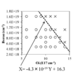
- FIG. 4 is a graph showing the relationship between the oxygen precipitate density, the initial oxygen concentration, and the boron concentration.
- the horizontal axis represents the oxygen concentration ( ⁇ 10 17 atoms / cm 3 ), and the vertical axis represents the boron concentration (atoms / cm 3 ). Is shown.
- the plot mark of the sample whose oxygen precipitate density was 1 ⁇ 10 10 pieces / cm 3 or less was “ ⁇ ”, and the plot mark of the sample that was more than 1 ⁇ 10 10 pieces / cm 3 was “ ⁇ ”. did.
- the oxygen precipitate density of 1 ⁇ 10 10 atoms / cm 3 or less cannot be satisfied unless the initial oxygen concentration is lowered as the boron concentration is higher.
- the maximum value of the initial oxygen concentration that can satisfy the oxygen precipitate density of 1 ⁇ 10 10 atoms / cm 3 or less is about 14 ⁇ 10 17. atoms / cm 3 .
- the maximum value of the initial oxygen concentration that can satisfy the oxygen precipitate density of 1 ⁇ 10 10 atoms / cm 3 or less is about 9 ⁇ 10 17. atoms / cm 3 .
- the boundary line between the plot marks “ ⁇ ” and “ ⁇ ” was expressed by a linear function of oxygen concentration and boron concentration, and the region of the plot mark “ ⁇ ” was defined. From the above results, when the oxygen concentration X ( ⁇ 10 17 atoms / cm 3 ) and the boron concentration Y (atoms / cm 3 ) satisfy the condition of X ⁇ ⁇ 4.3 ⁇ 10 ⁇ 19 Y + 16.3, It became clear that the density of precipitates could be 1 ⁇ 10 10 pieces / cm 3 or less.
Landscapes
- Chemical & Material Sciences (AREA)
- Engineering & Computer Science (AREA)
- Crystallography & Structural Chemistry (AREA)
- Materials Engineering (AREA)
- Metallurgy (AREA)
- Organic Chemistry (AREA)
- Chemical Kinetics & Catalysis (AREA)
- General Chemical & Material Sciences (AREA)
- Physics & Mathematics (AREA)
- Thermal Sciences (AREA)
- Crystals, And After-Treatments Of Crystals (AREA)
Abstract
Description

11 シリコン基板
12 エピタキシャル層
Claims (2)
- ボロンがドープされたシリコン基板の表面にエピタキシャル層が形成されたエピタキシャルシリコンウェーハであって、
前記シリコン基板中のボロン濃度が2.7×10¹⁷atoms/cm3以上かつ1.3×1019atoms/cm3以下であり、
前記シリコン基板中の初期酸素濃度が11×1017atoms/cm3以下であり、
前記エピタキシャルシリコンウェーハに対して酸素析出物評価熱処理を施した場合に、前記シリコン基板中の酸素析出物密度が1×10¹⁰個/cm3以下であることを特徴とするエピタキシャルシリコンウェーハ。 - 前記ボロン濃度Y(atoms/cm3)および前記初期酸素濃度X(×1017atoms/cm3)が、X≦-4.3×10-19Y+16.3の関係式を満たす、請求項1に記載のエピタキシャルシリコンウェーハ。
Priority Applications (5)
| Application Number | Priority Date | Filing Date | Title |
|---|---|---|---|
| DE112016003412.1T DE112016003412B4 (de) | 2015-07-28 | 2016-07-06 | Verfahren zur Herstellung eines Siliziumepitaxialwafer |
| US15/745,174 US20180204960A1 (en) | 2015-07-28 | 2016-07-06 | Epitaxial silicon wafer |
| CN201680043772.0A CN107849731A (zh) | 2015-07-28 | 2016-07-06 | 外延硅晶片 |
| KR1020187000940A KR102057086B1 (ko) | 2015-07-28 | 2016-07-06 | 에피택셜 실리콘 웨이퍼의 제조 방법 |
| US16/583,732 US10861990B2 (en) | 2015-07-28 | 2019-09-26 | Epitaxial silicon wafer |
Applications Claiming Priority (2)
| Application Number | Priority Date | Filing Date | Title |
|---|---|---|---|
| JP2015148558A JP6610056B2 (ja) | 2015-07-28 | 2015-07-28 | エピタキシャルシリコンウェーハの製造方法 |
| JP2015-148558 | 2015-07-28 |
Related Child Applications (2)
| Application Number | Title | Priority Date | Filing Date |
|---|---|---|---|
| US15/745,174 A-371-Of-International US20180204960A1 (en) | 2015-07-28 | 2016-07-06 | Epitaxial silicon wafer |
| US16/583,732 Continuation US10861990B2 (en) | 2015-07-28 | 2019-09-26 | Epitaxial silicon wafer |
Publications (1)
| Publication Number | Publication Date |
|---|---|
| WO2017018141A1 true WO2017018141A1 (ja) | 2017-02-02 |
Family
ID=57884539
Family Applications (1)
| Application Number | Title | Priority Date | Filing Date |
|---|---|---|---|
| PCT/JP2016/069980 Ceased WO2017018141A1 (ja) | 2015-07-28 | 2016-07-06 | エピタキシャルシリコンウェーハ |
Country Status (7)
| Country | Link |
|---|---|
| US (2) | US20180204960A1 (ja) |
| JP (1) | JP6610056B2 (ja) |
| KR (1) | KR102057086B1 (ja) |
| CN (1) | CN107849731A (ja) |
| DE (1) | DE112016003412B4 (ja) |
| TW (1) | TWI605494B (ja) |
| WO (1) | WO2017018141A1 (ja) |
Families Citing this family (4)
| Publication number | Priority date | Publication date | Assignee | Title |
|---|---|---|---|---|
| JP7142184B2 (ja) * | 2020-08-18 | 2022-09-26 | 信越半導体株式会社 | 窒化物半導体ウェーハの製造方法及び窒化物半導体ウェーハ |
| TWI792462B (zh) * | 2021-07-30 | 2023-02-11 | 合晶科技股份有限公司 | 供磊晶成長的複合基板及其製作方法 |
| CN113782423B (zh) * | 2021-08-25 | 2022-08-23 | 中国科学院宁波材料技术与工程研究所 | 杂质扩散方法和太阳能电池制造方法 |
| JP7632261B2 (ja) * | 2021-12-17 | 2025-02-19 | 株式会社Sumco | シリコンウェーハ及びその製造方法 |
Citations (2)
| Publication number | Priority date | Publication date | Assignee | Title |
|---|---|---|---|---|
| JP2006040972A (ja) * | 2004-07-22 | 2006-02-09 | Shin Etsu Handotai Co Ltd | シリコンエピタキシャルウェーハおよびその製造方法 |
| JP2010083712A (ja) * | 2008-09-30 | 2010-04-15 | Sumco Corp | 結晶欠陥状態予測方法、シリコンウェーハの製造方法 |
Family Cites Families (16)
| Publication number | Priority date | Publication date | Assignee | Title |
|---|---|---|---|---|
| TW331017B (en) * | 1996-02-15 | 1998-05-01 | Toshiba Co Ltd | Manufacturing and checking method of semiconductor substrate |
| JPH10303208A (ja) * | 1997-04-30 | 1998-11-13 | Toshiba Corp | 半導体基板およびその製造方法 |
| KR100541882B1 (ko) * | 1998-05-01 | 2006-01-16 | 왁커 엔에스씨이 코포레이션 | 실리콘 반도체 기판 및 그의 제조 방법 |
| JP4510997B2 (ja) * | 2000-01-18 | 2010-07-28 | シルトロニック・ジャパン株式会社 | シリコン半導体基板およびその製造方法 |
| CA2504820C (en) * | 2002-11-06 | 2011-08-23 | Grelan Pharmaceutical Co., Ltd. | Pyrazolonaphthyridine derivatives |
| JP4983161B2 (ja) * | 2005-10-24 | 2012-07-25 | 株式会社Sumco | シリコン半導体基板およびその製造方法 |
| JP4853237B2 (ja) | 2006-11-06 | 2012-01-11 | 株式会社Sumco | エピタキシャルウェーハの製造方法 |
| JP2010141272A (ja) * | 2008-12-15 | 2010-06-24 | Sumco Corp | エピタキシャルウェーハとその製造方法 |
| KR101389058B1 (ko) * | 2009-03-25 | 2014-04-28 | 가부시키가이샤 사무코 | 실리콘 웨이퍼 및 그 제조방법 |
| JP5504664B2 (ja) * | 2009-03-25 | 2014-05-28 | 株式会社Sumco | シリコンエピタキシャルウェーハおよびその製造方法 |
| JP2011021898A (ja) * | 2009-07-13 | 2011-02-03 | Fujitsu Ltd | 走査プローブ顕微鏡用標準試料及びキャリア濃度測定方法 |
| JP2011228459A (ja) | 2010-04-19 | 2011-11-10 | Sumco Corp | シリコンウェーハ及びその製造方法 |
| TW201234570A (en) | 2010-12-09 | 2012-08-16 | Sumco Corp | Epitaxial substrate for back-illuminated solid-state imaging device, and method of manufacturing the same |
| JP2012151458A (ja) * | 2010-12-27 | 2012-08-09 | Elpida Memory Inc | 半導体装置及びその製造方法 |
| WO2014041736A1 (ja) * | 2012-09-13 | 2014-03-20 | パナソニック株式会社 | 窒化物半導体構造物 |
| US9634098B2 (en) * | 2013-06-11 | 2017-04-25 | SunEdison Semiconductor Ltd. (UEN201334164H) | Oxygen precipitation in heavily doped silicon wafers sliced from ingots grown by the Czochralski method |
-
2015
- 2015-07-28 JP JP2015148558A patent/JP6610056B2/ja active Active
-
2016
- 2016-06-21 TW TW105119403A patent/TWI605494B/zh active
- 2016-07-06 US US15/745,174 patent/US20180204960A1/en not_active Abandoned
- 2016-07-06 KR KR1020187000940A patent/KR102057086B1/ko active Active
- 2016-07-06 CN CN201680043772.0A patent/CN107849731A/zh active Pending
- 2016-07-06 DE DE112016003412.1T patent/DE112016003412B4/de active Active
- 2016-07-06 WO PCT/JP2016/069980 patent/WO2017018141A1/ja not_active Ceased
-
2019
- 2019-09-26 US US16/583,732 patent/US10861990B2/en active Active
Patent Citations (2)
| Publication number | Priority date | Publication date | Assignee | Title |
|---|---|---|---|---|
| JP2006040972A (ja) * | 2004-07-22 | 2006-02-09 | Shin Etsu Handotai Co Ltd | シリコンエピタキシャルウェーハおよびその製造方法 |
| JP2010083712A (ja) * | 2008-09-30 | 2010-04-15 | Sumco Corp | 結晶欠陥状態予測方法、シリコンウェーハの製造方法 |
Also Published As
| Publication number | Publication date |
|---|---|
| JP2017024965A (ja) | 2017-02-02 |
| JP6610056B2 (ja) | 2019-11-27 |
| CN107849731A (zh) | 2018-03-27 |
| DE112016003412B4 (de) | 2025-10-16 |
| US20180204960A1 (en) | 2018-07-19 |
| DE112016003412T5 (de) | 2018-04-19 |
| KR20180016580A (ko) | 2018-02-14 |
| TW201715579A (zh) | 2017-05-01 |
| KR102057086B1 (ko) | 2019-12-18 |
| US20200020817A1 (en) | 2020-01-16 |
| TWI605494B (zh) | 2017-11-11 |
| US10861990B2 (en) | 2020-12-08 |
Similar Documents
| Publication | Publication Date | Title |
|---|---|---|
| KR100875228B1 (ko) | 반도체용 실리콘 웨이퍼 및 그 제조방법 | |
| CN107533959B (zh) | 外延硅晶片的制造方法 | |
| JP6020342B2 (ja) | シリコンエピタキシャルウェーハ及びシリコンエピタキシャルウェーハの製造方法 | |
| JP5343371B2 (ja) | シリコン基板とその製造方法 | |
| US10211066B2 (en) | Silicon epitaxial wafer and method of producing same | |
| US10861990B2 (en) | Epitaxial silicon wafer | |
| WO2015107562A1 (ja) | シリコンウェーハおよびその製造方法 | |
| US20090226736A1 (en) | Method of manufacturing silicon substrate | |
| CN114174569B (zh) | 碳掺杂单晶硅晶圆及其制造方法 | |
| WO2006117939A1 (ja) | シリコンウェーハの製造方法 | |
| CN106133186A (zh) | 硼掺杂的n型硅靶材 | |
| JP6973475B2 (ja) | エピタキシャルシリコンウェーハの製造方法およびエピタキシャルシリコンウェーハ | |
| KR102808350B1 (ko) | 탄소도프 실리콘 단결정 웨이퍼 및 그의 제조방법 | |
| JP2011023533A (ja) | シリコン基板とその製造方法 | |
| JP2011003577A (ja) | シリコンウェーハ及びその製造方法、並びに、半導体デバイスの製造方法 | |
| KR100734615B1 (ko) | N-형 반도체 잉곳 및 그 제조 방법 | |
| JP2024038818A (ja) | シリコンウェーハおよびエピタキシャルシリコンウェーハ | |
| JP2005089246A (ja) | 砒素ドープシリコンウェーハの製造方法 |
Legal Events
| Date | Code | Title | Description |
|---|---|---|---|
| 121 | Ep: the epo has been informed by wipo that ep was designated in this application |
Ref document number: 16830246 Country of ref document: EP Kind code of ref document: A1 |
|
| ENP | Entry into the national phase |
Ref document number: 20187000940 Country of ref document: KR Kind code of ref document: A |
|
| WWE | Wipo information: entry into national phase |
Ref document number: 15745174 Country of ref document: US |
|
| WWE | Wipo information: entry into national phase |
Ref document number: 112016003412 Country of ref document: DE |
|
| 122 | Ep: pct application non-entry in european phase |
Ref document number: 16830246 Country of ref document: EP Kind code of ref document: A1 |
|
| WWG | Wipo information: grant in national office |
Ref document number: 112016003412 Country of ref document: DE |