WO2017013839A1 - 電子装置及び電子装置の製造方法 - Google Patents
電子装置及び電子装置の製造方法 Download PDFInfo
- Publication number
- WO2017013839A1 WO2017013839A1 PCT/JP2016/003110 JP2016003110W WO2017013839A1 WO 2017013839 A1 WO2017013839 A1 WO 2017013839A1 JP 2016003110 W JP2016003110 W JP 2016003110W WO 2017013839 A1 WO2017013839 A1 WO 2017013839A1
- Authority
- WO
- WIPO (PCT)
- Prior art keywords
- electronic device
- land
- solder
- circuit board
- facing
- Prior art date
- Legal status (The legal status is an assumption and is not a legal conclusion. Google has not performed a legal analysis and makes no representation as to the accuracy of the status listed.)
- Ceased
Links
Images




Classifications
-
- H—ELECTRICITY
- H05—ELECTRIC TECHNIQUES NOT OTHERWISE PROVIDED FOR
- H05K—PRINTED CIRCUITS; CASINGS OR CONSTRUCTIONAL DETAILS OF ELECTRIC APPARATUS; MANUFACTURE OF ASSEMBLAGES OF ELECTRICAL COMPONENTS
- H05K1/00—Printed circuits
- H05K1/18—Printed circuits structurally associated with non-printed electric components
-
- H—ELECTRICITY
- H05—ELECTRIC TECHNIQUES NOT OTHERWISE PROVIDED FOR
- H05K—PRINTED CIRCUITS; CASINGS OR CONSTRUCTIONAL DETAILS OF ELECTRIC APPARATUS; MANUFACTURE OF ASSEMBLAGES OF ELECTRICAL COMPONENTS
- H05K3/00—Apparatus or processes for manufacturing printed circuits
- H05K3/30—Assembling printed circuits with electric components, e.g. with resistors
- H05K3/32—Assembling printed circuits with electric components, e.g. with resistors electrically connecting electric components or wires to printed circuits
- H05K3/34—Assembling printed circuits with electric components, e.g. with resistors electrically connecting electric components or wires to printed circuits by soldering
Definitions
- the present disclosure relates to an electronic device in which a land formed on a circuit board and an electrode of a mounted component are joined by solder, and a method for manufacturing the electronic device.
- Patent Document 1 Conventionally, as an example of an electronic apparatus having the above-described configuration, there is a technique disclosed in Patent Document 1.
- Patent Literature 1 a land formed on a printed circuit board as a circuit board and an electrode of a chip component as a mounting component are joined by solder.
- a material in which a flux component is previously applied to the solder material may be used.
- a flux component remains on the surface of the circuit board after soldering and the surface of the mounted component.
- the residual flux component can be removed by a cleaning process.
- the cleaning process is performed by, for example, immersing an electronic device in which a mounting component is mounted on a circuit board in a cleaning liquid and eluting a residual flux component into the cleaning liquid.
- a facing space sandwiched between the circuit board and the mounting component is formed. The flux component formed in the facing space tends to remain without being removed by the cleaning liquid.
- the present disclosure has been made in view of the above points, and an object thereof is to provide an electronic device and a method for manufacturing the electronic device that can suppress the flux component from remaining between the electrodes.
- An electronic device includes a circuit board having two lands that are a part of wiring, and a mounting that is mounted on the circuit board and has two electrodes individually facing each of the lands.
- the opposing region of one electrode includes a region where the land and the solder are disposed and a region where the land and the solder are not disposed, and the opposing region of the other electrode includes at least a region where the land and the solder are disposed.
- a facing space is formed which is sandwiched between two solders and is open at both ends.
- the facing space includes a narrow portion having an opening area narrower than the opening area at both ends of itself.
- the above electronic device it is possible to have a configuration that can improve the cleaning performance of the solder flux component, that is, a configuration that can shorten the cleaning time, and it is possible to suppress the flux component from remaining between the electrodes.
- a method for manufacturing an electronic device according to a second aspect of the present disclosure is a method for manufacturing an electronic device according to the first aspect, wherein a constituent material of solder including a flux component is provided between each electrode and each land. By melting and curing the material, joining each electrode and each land with solder, and then immersing the electronic device in a cleaning solution to remove the flux component adhering to the surface of the electronic device including.
- the cleaning time can be shortened and the flux component can be prevented from remaining between the electrodes.
- the time for removing the flux component by washing can be shortened, the electronic device can be manufactured in a short time.
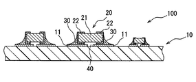
- FIG. 1 is a plan view illustrating a schematic configuration of the electronic device according to the first embodiment of the present disclosure.
- FIG. 2 is a sectional view taken along line II-II in FIG.
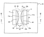
- FIG. 3 is a plan view showing a schematic configuration of the circuit board in the first embodiment.
- 4 is a cross-sectional view taken along line IV-IV in FIG.
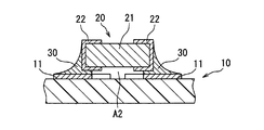
- FIG. 5 is a cross-sectional view taken along line VV in FIG.
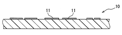
- FIG. 6 is a cross-sectional view showing a schematic configuration of the circuit board in the first embodiment.
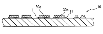
- FIG. 7 is a cross-sectional view illustrating a schematic configuration of the circuit board in a state where the solder paste is provided in the first embodiment.
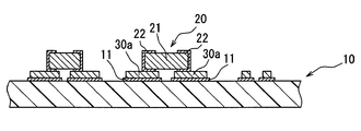
- FIG. 8 is a cross-sectional view illustrating a schematic configuration of the circuit board in a state where the mounting component according to the first embodiment is provided.
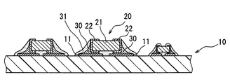
- FIG. 9 is a cross-sectional view illustrating a schematic configuration of the circuit board after reflow in the first embodiment.
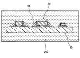
- FIG. 10 is a cross-sectional view illustrating a schematic configuration of the circuit board during cleaning in the first embodiment.
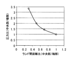
- FIG. 11 is a graph showing the relationship between the land-to-land distance ratio and the pressure ratio in the first embodiment,
- FIG. 12 is a plan view illustrating a schematic configuration of a circuit board according to the second embodiment of the present disclosure.
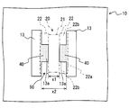
- FIG. 13 is a plan view illustrating a schematic configuration of a circuit board according to the third embodiment of the present disclosure.
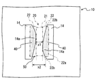
- FIG. 14 is a plan view illustrating a schematic configuration of a circuit board according to the fourth embodiment of the present disclosure.
- FIG. 15 is a plan view illustrating a schematic configuration of a circuit board according to the fifth embodiment of the present disclosure.
- the electronic device 100 includes a circuit board 10, a mounting component 20 mounted on the circuit board 10, and a solder 30 that joins the circuit board 10 and the mounting component 20. Configured.
- the circuit board 10 is formed by wiring on an insulating base material such as resin or ceramics using a conductor pattern such as Cu or Ag. Moreover, the circuit board 10 can employ, for example, a multilayer board in which conductor patterns are laminated via an insulating base material.
- the mounting component 20 is mounted on one surface of the circuit board 10. It can be said that the surface of the circuit board 10 on which the mounting component 20 is mounted is a mounting surface.
- the circuit board 10 has lands 11 that are part of the wiring formed on the mounting surface. That is, the land 11 is a part formed flat on the mounting surface as part of the wiring. Further, the land 11 is a part joined to the electrode 22 of the mounting component 20 and can be said to be a mounting land.
- a mounting component 20 that is a two-terminal element having two electrodes 22 is employed.
- the circuit board 10 in which the pair of lands 11, that is, the two lands 11 are formed on one mounting component 20 is employed.
- the present disclosure is not limited to this.
- the circuit board 10 is formed with the same number of lands 11 as the lands 11 on which the mounting component 20 is mounted. Will be.
- the electrodes 22 are arranged to face each other, and are electrically and mechanically connected to the electrodes 22 through the solder 30. That is, in the two lands 11, one electrode 22 is disposed opposite to one land 11 and is joined to the electrodes 22 disposed opposite to each other. In FIG. 1, the land 11 is disposed at a position hidden behind the solder 30.
- the land 11 has, for example, a thickness of 10 ⁇ m or more, and preferably 30 to 80 ⁇ m.
- the land 11 has a convex portion 11a as shown in FIG.
- the pair of lands 11 are arranged such that the vertices of the convex portions 11a face each other.
- the land 11 is formed with a convex portion 11 a having a curved portion at a portion facing the land 11 disposed facing the land 11.
- the distance between the pair of lands 11 is shortened from both ends of each facing portion toward the center. That is, in the pair of lands 11, the distance at the center of each facing part is narrower than the distance between both ends of each facing part. Note that at least a part of the convex portion 11 a is disposed to face the mounting component 20.
- each land 11 intersects with two places on opposite sides of the electrode 22 arranged to face each other, and also intersects with one place on each end side.
- the two lands 11 have a convex portion 11 a opposed to a part of the electrode 22. That is, it can be said that each land 11 and each electrode 22 are arranged so that only a part thereof overlaps.
- the mounting component 20 includes a base 21 and an electrode 22 formed on the base 21.
- the mounting component 20 is mounted on the circuit board 10 and has two electrodes 22 individually facing the lands 11.
- Each electrode 22 includes a portion facing the mounting surface in a state where the mounting component 20 is mounted on the circuit board 10.
- the mounting component 20 has two electrodes 22 arranged in parallel.
- the mounting component 20 can employ a passive element such as a chip resistor or a chip capacitor.
- each electrode 22 can be referred to as a side facing the electrode 22 arranged to be opposed, and can be referred to as a side corresponding to the element end. Therefore, it can be said that each electrode 22 includes two end sides and opposite sides that are connected to two short sides.
- the opposing region of each electrode 22 includes an arrangement region 22a where the land 11 and the solder 30 are arranged, and a non-arrangement region 22b where the land 11 and the solder 30 are not arranged.
- the facing region of each electrode 22 corresponds to a projection region of the surface of each electrode 22 facing the mounting surface.
- region of each electrode 22 is an area
- a reference numeral 40 in FIG. 3 is a joint portion in which the electrode 22 and the land 11 are joined by the solder 30. Therefore, the arrangement region 22a and the joint portion 40 can be regarded as the same range. Further, the electrode 22 and the solder 30 are not joined in the non-arrangement region 22b. In this way, only a part of the portion of the electrode 22 that faces the mounting surface is joined to the land 11 via the solder 30. Note that FIG. 3 is not a cross-sectional view, but is hatched to make the joint 40 and other regions clear.
- the facing region of one electrode 22 includes the placement region 22a and the non-placement region 22b, and the facing region of the other electrode 22 may include at least the placement region 22a. That is, one of the two electrodes 22 may be bonded to the land 11 through the solder 30 in the entire area of the surface facing the circuit board 10.
- a long-side electrode component having a longer length along the two electrodes than the interval between the two electrodes 22 is employed as the mounting component 20.
- the long-side electrode component is a component in which the ratio of the depth x3 of the space formed under the long-side electrode component and the distance x1 between the pair of electrodes 22 is 2.0 or more when mounted on the circuit board 10. It is.
- the depth length is equal to the component length of the long side electrode component.
- the mounting component 20 can be a short-side electrode component.
- the short-side electrode component is a component in which the length along the two electrodes is shorter than the interval between the two electrodes 22, or the interval between the two electrodes 22 and the length along the two electrodes are equal.
- the mounting component 20 may be a bare chip-shaped semiconductor element in which an electrode is formed on a base mainly composed of a semiconductor, a packaged electronic component, or the like.
- the electronic device 100 includes two solders 30 for one mounting component 20.
- the solder 30 is obtained after the reflow process in a state where the solder paste 30a is disposed between the land 11 and the electrode 22.
- a solder paste 30a which is a constituent material of the solder 30, is obtained by mixing a solder fine powder and a flux component 31 into a cream.
- the alloy constituting the solder fine powder include Sn-based alloys such as Sn-Cu, Sn-Pb, Sn-Pb-Ag, and Sn-Pb-Bi, In-based alloys such as In-Pb, and Pb-Ag.
- the Pb-based alloy is mentioned.
- the flux component 31 is composed of rosin that removes an oxide film on the surface of the base material, an activator that promotes solderability, a solvent involved in printability, and the like.
- the solder 30 is formed on the land 11. For this reason, as described above, the solder 30 is joined to the non-arrangement region 22b of the mounting component 20 while the solder 30 is joined to the placement region 22a. Further, the solder 30 is not connected to the base 21 exposed from the electrode 22 in the mounting component 20. In other words, in the electronic device 100, in the region sandwiched between the circuit board 10 and the mounting component 20, the solder 30 is formed only in the region where the land 11 and the arrangement region 22 a face each other to form the joint 40.
- a facing space 50 that is sandwiched between two solders 30 and that is open at both ends is formed in a region where the circuit board 10 and the mounting component 20 face each other.
- the open end in the facing space 50 can be said to be the opening end of the facing space 50.
- the electronic device 100 has an opening end of the facing space 50 formed between the element end of the mounting component 20 and the circuit board 10.
- the opposing space 50 includes a narrow portion between the two ends of the opposing space 50 where the interval between the two solders 30 is narrower than the interval between the two solders 30 at both ends thereof. That is, in the electronic device 100, the interval x1 of the central solder 30 in the opposing space 50 is smaller than the interval x2 of the solder 30 at both ends in the opposing space 50 (x1 ⁇ x2). In other words, the electronic device 100 includes a portion in the facing space 50 where the interval between the two junctions 40 is narrower than the interval between the two junctions 40 at both ends.
- the distance between the joint portions 40 gradually decreases from both ends of the counter space 50 toward the center of the counter space 50, and the distance between the joint portions 40 is constant within a predetermined range including the center of the counter space 50.
- An electronic device 100 is employed. Note that the interval x1 and the interval x2 can also be said to be the interval of the joint portion 40.
- the electronic device 100 can be said to have a central opening area A ⁇ b> 1 in the facing space 50 smaller than the opening area A ⁇ b> 2 at the opening end in the facing space 50.
- the facing space 50 includes a region having an opening area smaller than the opening area A2 at the opening end.
- the opening area corresponds to an area in a range along a virtual plane orthogonal to the two electrodes 22 in the facing space 50. Further, the distance between one opening end and the other opening end can be said to be the depth of the facing space 50.
- an electronic device in which the dimension under the mounting component 20 after soldering is 0.07 to 0.15 mm in height, the distance between the electrodes 22 is 0.5 mm, and the depth is 3.5 mm.
- the apparatus 100 is employed.
- the height is a distance between the circuit board 10 and the mounting component 20.
- the electronic device 100 may include a sealing resin that integrally covers the mounting surface of the circuit board 10 and the mounting component 20. Further, the electronic device 100 may include a mounting component having three or more electrodes 22 and a circuit board on which lands individually corresponding to the electrodes of the mounting component are formed.
- This manufacturing method includes first to fifth steps described below.
- a circuit board 10 on which lands 11 are formed is prepared.
- a solder paste 30a is formed on the land 11 (joining step).
- a predetermined amount of solder paste 30a is formed on the land by application using a dispenser or screen printing.
- the mounting component 20 is mounted on the solder paste 30a (joining step). At this time, since the solder paste 30a is not cured, the land 11 and the electrode 22 are not firmly fixed.
- the solder paste 30a is melted and cured to join the electrodes 22 and the lands 11 with the solder 30 (joining step). That is, the fourth process can be said to be a reflow process. In this way, the circuit board 10 and the mounting component 20 are joined via the solder 30.
- the solder paste 30a contains the flux component 31 as described above.
- the flux component 31 adheres to the surface of the circuit board 10, the mounted component 20, and the solder 30 after the reflow process. Further, the flux component 31 flows so as to cover the solder 30 and flows into the facing space 50. That is, when the fourth step is completed, the flux component 31 is attached to the surface of the electronic device 100. The remaining flux component 31 may hinder mounting processing in a later process. Further, the remaining flux component 31 can cause migration.
- the fifth step of removing the flux component 31 remaining on the surface of the electronic device 100 is performed. That is, the fifth step corresponds to a cleaning step.
- the electronic device 100 to which the flux component 31 is attached is immersed in the cleaning liquid 200.
- the electronic device 100 to which the flux component 31 is attached is left in a state where it is immersed in the cleaning liquid 200, so that the flux component 31 is eluted and removed from the portion in contact with the cleaning liquid 200.
- the flux component 31 adhering to the electronic device 100 can be removed.
- the electronic device 100 since the flux component 31 is removed, the electronic device 100 capable of suppressing the occurrence of migration can be manufactured. Moreover, this manufacturing method can suppress that the mounting process is inhibited by the flux component 31 when the electronic device 100 is mounted after the fifth step. Furthermore, since the electronic device 100 can secure a bonding area at the center of the land 11 having a low stress generated during the cooling / heating cycle test, the electronic device 100 can have a long life.
- the time required for elution of the flux component 31 is determined by the amount of the remaining flux component 31 and the circulation amount of the cleaning liquid 200 around the flux component 31. Note that the amount of the flux component 31 can also be regarded as the thickness of the flux component 31. The time required for elution of the flux component 31 can also be said to be a cleaning time.
- the electronic device 100 includes the narrow space having an opening area narrower than the opening area at both ends of the facing space in the facing space 50.
- the electronic device 100 can increase the pressure difference of the cleaning liquid 200.
- the pressure of the cleaning liquid 200 can be larger at the narrow part than at both ends in the facing space 50.
- the land end portion has a wider distance between the lands than the center portion. 50, the pressure difference of the cleaning liquid 200 can be increased.
- the horizontal axis is a value obtained by dividing the size of the center of the land 11 by the size of the end of the land 11
- the vertical axis is a value obtained by dividing the pressure of the center of the land 11 by the pressure of the end of the land 11. is there.
- the dimension is a distance between the lands 11.
- the cleaning liquid 200 including the flux component 31 flows from the central portion in the facing space 50 to the opening end side. For this reason, in the fifth step, the fresh cleaning liquid 200 flows into the facing space 50 and the melting ability of the flux component 31 can be maintained.
- Equation 1 The relationship between the liquid flow rate and the flow velocity in the tunnel shape is expressed by Equation 1.
- Equation 2 Substituting Equation 2 into Equation 1 and converting it to P.
- the electronic device 100 when the circuit board 10 and the mounting component 20 after the bonding process are immersed in the cleaning liquid 200, the cleaning liquid 200 easily flows from the position sandwiched between both opening ends in the facing space 50 to both opening ends. Become. Therefore, the electronic device 100 can have a configuration that can improve the cleaning properties of the flux component 31, that is, a configuration that can shorten the cleaning time, and can prevent the flux component 31 from remaining between the electrodes 22. In addition, it can be said that the electronic device 100 has a structure that can shorten the cleaning time.
- this manufacturing method removes the remaining flux component 31 by immersing the electronic device 100 including the narrow portion in the cleaning liquid 200, the cleaning performance of the flux component 31 in the fifth step can be improved. It is possible to suppress the flux component 31 from remaining between 22.
- the cleaning time may become longer as the depth of the facing space 50 becomes longer. all right.
- the land becomes wider and the amount of solder paste increases, as a result, compared to the case where the short-side electrode component of the same physique is mounted. The amount of ingredients will also increase.
- the facing space becomes narrower than when the short-side electrode component having the same physique is mounted, and the circulation amount of the cleaning liquid is also reduced. Therefore, in the electronic device, when the long-side electrode component is mounted, the time required to remove the flux component remaining in the facing space is longer than when the short-side electrode component having the same physique is mounted. .
- the long-side electrode component is adopted as the mounting component 20.
- the cleaning liquid 200 easily flows toward both ends. Therefore, the flux component 31 is removed by cleaning while adopting a long-side electrode component as the mounting component 20. Time can be shortened. Moreover, since this manufacturing method can shorten the time which removes the flux component 31 by washing
- the distance between the lands 11 is made wider than the distance between the electrodes 22 in order to widen the facing space 50 and shorten the cleaning time while adopting a long-side electrode part as the mounting part 20.
- the electronic device 100 can shorten the cleaning time while suppressing a reduction in the bonding area between the land 11 and the electrode 22. Therefore, the electronic device 100 can shorten the cleaning time while maintaining the bonding reliability between the land 11 and the electrode 22.
- the electrode and the land are joined via the solder, and the mounting component is mounted on the circuit board. Further, according to the present disclosure, a facing space that is sandwiched between two solders and that is open at both ends is formed in a region where the circuit board and the mounting component face each other.
- the flux component is formed on the surface of the solder after the joining process. Further, the flux component is also formed in the facing space. Usually, this flux component is cleaned (removed) by immersing the circuit board and the mounted component in a cleaning solution after the joining step.
- the electronic device includes a narrow portion in the facing space that has an opening area that is narrower than the opening area at both ends of the facing space.
- this indication can enlarge the pressure difference of cleaning fluid.
- the pressure of the cleaning liquid can be larger at the narrow part than at both ends in the facing space.
- this indication can have the composition which can improve the washing nature of the flux ingredient of solder, ie, the composition which can shorten washing time, and can control that the flux ingredient remains between electrodes.
- the present disclosure provides a method for manufacturing an electronic device in which an electrode and a land are joined via solder and a mounting component is mounted on a circuit board.
- a facing space that is sandwiched between two solders and that is open at both ends is formed in a region where the circuit board and the mounting component face each other.
- a solder constituent material containing a flux component is provided between each electrode and each land, and the constituent material is melted and hardened to thereby connect each electrode and each land. Join with solder. Then, this indication immerses a circuit board and mounting parts in cleaning fluid, and removes a flux ingredient generated at a joining process. The flux component generated in the joining process is also formed in the facing space.
- the electronic device includes a narrow portion in the facing space that has an opening area that is narrower than the opening area at both ends of the facing space.
- the electronic device can increase the pressure difference of the cleaning liquid.
- the pressure of the cleaning liquid can be larger at the narrow part than at both ends in the facing space.
- this indication can improve the washing nature of the flux ingredient of solder, ie, it can shorten washing time and can control that a flux ingredient remains between electrodes.
- this indication can shorten the time which removes a flux component by washing
- Modification 1 The electronic device of the modification 1 is demonstrated using FIG.
- the electronic device of Modification 1 is different from the electronic device 100 in the shape of the land 12.
- Each land 12 has a triangular portion in the plan view shown in FIG. Further, each land 12 differs from the land 11 in the plan view shown in FIG. 12, but intersects with one portion of each end side of the electrode 22 disposed facing the land 12, but does not intersect with the facing side.
- Each land 12 does not have to intersect with each end side of the electrode 22.
- a facing space 50 similar to the electronic device 100 is formed.
- the electronic device of Modification 1 can achieve the same effects as the electronic device 100.
- each land 13 has a rectangular shape in the plan view shown in FIG.
- Each land 13 unlike the land 11, intersects with one portion of each end side of the electrode 22 disposed so as to face the land 22 in a plan view shown in FIG. 13, but does not intersect with the facing side.
- each land 13 is formed with a convex portion 13 a protruding from the periphery at a portion facing the electrode 22.
- Each land 13 does not need to intersect each end side of the electrode 22.
- the electronic device of the present modification a facing space 50 similar to the electronic device 100 is formed. Therefore, the electronic device of Modification 2 can achieve the same effect as the electronic device 100.
- each land 14 has a convex portion 14 a having a curved portion at a facing portion in a plan view shown in FIG. 14. Further, each land 14 is different from the land 11, but intersects with one portion of each end side of the electrode 22 disposed facing the land 22 in a plan view shown in FIG. 14, but does not intersect with the facing side. Further, the pair of lands 14 are arranged at positions shifted from each other without the vertices of the convex portions 14a facing each other. Each land 14 does not have to intersect with each end side of the electrode 22.
- the electronic device of the present modification a facing space 50 similar to the electronic device 100 is formed. Therefore, the electronic device of Modification 3 can achieve the same effects as the electronic device 100.
- Modification 4 The electronic device of the modification 4 is demonstrated using FIG.
- the electronic device of Modification 4 is different from the electronic device 100 in the shapes of the mounting component 20 a and the lands 151 and 152.
- the mounting component 20a is a bare-chip semiconductor element.
- the mounting component 20a can also be said to be a power semiconductor element.
- the mounting component 20a has a drain electrode formed on one surface, and a gate electrode 221 and a source electrode 222 formed on the opposite surface.
- the mounting component 20 a is mounted on the circuit board 10 with the opposite surface facing the circuit board 10. The mounting component 20a can be used even if the emitter electrode is formed on one surface and the base electrode and the collector electrode are formed on the opposite surface.
- the circuit board 10 includes a gate land 151 and a source land 152 corresponding to the mounting component 20a.
- the electronic device of Modification 4 is different from the electronic device 100 in this point.
- the circuit board 10 of Modification 4 is different from the circuit board 10 in that the gate land 151 and the source land 152 are formed, but for convenience, the same reference numerals as those in the above embodiment are given.
- the gate electrode 221 and the gate land 151 are joined by the solder 30, and the source electrode 222 is connected by the source land 152 and the solder 30.
- the opposing region of the source electrode 222 includes an arrangement region 22a where the source land 152 and the solder 30 are arranged, and a non-arrangement region 22b where the source land 152 and the solder 30 are not arranged.
- the electronic device of the present modification forms a facing space 50 similar to that of the electronic device 100. For this reason, the electronic device of the modification 4 can have the same effect as the electronic device 100.
Landscapes
- Engineering & Computer Science (AREA)
- Microelectronics & Electronic Packaging (AREA)
- Manufacturing & Machinery (AREA)
- Electric Connection Of Electric Components To Printed Circuits (AREA)
Abstract
電子装置は、配線の一部である二つのランド(11)を有した回路基板(10)と、回路基板(10)に実装されておりランド(11)の夫々と個別に対向した二つの電極(22)を有した実装部品(20)と、ランド(11)と電極(22)におけるランド(11)が対向した部位とを接合している二つのはんだ(30)と、を備えている。回路基板(10)と実装部品(20)とが対向している領域には、二つのはんだで挟まれ、且つ、両端が開口した対向空間(50)が形成されている。この対向空間(50)は、自身の両端における開口面積よりも狭い開口面積である狭部位を含む。
Description
本出願は、2015年7月23日に出願された日本特許出願番号2015-145923号に基づくもので、ここにその記載内容を援用する。
本開示は、回路基板に形成されたランドと、実装部品の電極とがはんだによって接合された電子装置及び電子装置の製造方法に関する。
従来、上記のような構成の電子装置の一例として、特許文献1に開示された技術がある。特許文献1には、回路基板としてのプリント基板に形成されたランドと、実装部品としてのチップ部品の電極とがはんだによって接合されている。
はんだ付けは、はんだ材料にフラックス成分が予め付与された材料を用いることがある。この場合、はんだ付け後の回路基板の表面や実装部品の表面には、フラックス成分が残る。残留フラックス成分は、洗浄処理で除去することが考えられる。洗浄処理は、例えば、回路基板に実装部品が実装された電子装置を洗浄液に浸漬させて、残留フラックス成分を洗浄液に溶出させることで除去する。しかしながら、電子装置は、回路基板と実装部品とで挟まれた対向空間が形成される。この対向空間に形成されたフラックス成分は、洗浄液で除去されずに残りやすい。
本開示は、上記点に鑑みてなされたものであり、電極間にフラックス成分が残ることを抑制できる電子装置、及び電子装置の製造方法を提供することを目的とする。
本開示の第一態様による電子装置は、配線の一部である二つのランドを有した回路基板と、回路基板に実装されており、ランドの夫々と個別に対向した二つの電極を有した実装部品と、ランドと電極におけるランドが対向した部位とを接合している二つのはんだと、を備える。一つの電極の対向領域は、ランド及びはんだが配置された領域と、ランド及びはんだが配置されていない領域とを含み、他の電極の対向領域は、ランド及びはんだが配置された領域を少なくとも含み、回路基板と実装部品とが対向している領域には、二つのはんだで挟まれ、且つ、両端が開口した対向空間が形成されている。対向空間は、自身の両端における開口面積よりも狭い開口面積である狭部位を含む。
上記電子装置によると、はんだのフラックス成分の洗浄性を向上できる構成、すなわち、洗浄時間を短縮できる構成を有することができ、電極間にフラックス成分が残ることを抑制できる。
本開示の第2態様による電子装置の製造方法は、上記第1態様による電子装置の製造方法であって、各電極と各ランドとの間に、フラックス成分を含むはんだの構成材料を設け、構成材料を溶融及び硬化させことで、各電極と各ランドとをはんだによって接合する接合し、その後に、電子装置を洗浄液に浸漬して、電子装置の表面に付着しているフラックス成分を除去することを含む。
上記電子装置の製造方法によると、洗浄時間を短縮でき、電極間にフラックス成分が残ることを抑制できる。また、フラックス成分を洗浄により除去する時間を短縮できるため、その分、短時間で電子装置を製造できる。
本開示についての上記目的およびその他の目的、特徴や利点は、添付の図面を参照しながら下記の詳細な記述により、より明確になる。その図面は、
図1は、本開示の第1実施形態における電子装置の概略構成を示す平面図であり、
図2は、図1のII-II線に沿う断面図であり、
図3は、第1実施形態における回路基板の概略構成を示す平面図であり、
図4は、図3のIV-IV線に沿う断面図であり、
図5は、図3のV-V線に沿う断面図であり、
図6は、第1実施形態における回路基板の概略構成を示す断面図であり、
図7は、第1実施形態におけるはんだペーストが設けられた状態の回路基板の概略構成を示す断面図であり、
図8は、第1実施形態における実装部品が設けられた状態の回路基板の概略構成を示す断面図であり、
図9は、第1実施形態におけるリフロー後の回路基板の概略構成を示す断面図であり、
図10は、第1実施形態における洗浄時の回路基板の概略構成を示す断面図であり、
図11は、第1実施形態におけるランド間距離比と圧力比との関係を示すグラフであり、
図12は、本開示の第2実施形態における回路基板の概略構成を示す平面図であり、
図13は、本開示の第3実施形態における回路基板の概略構成を示す平面図であり、
図14は、本開示の第4実施形態における回路基板の概略構成を示す平面図であり、
図15は、本開示の第5実施形態における回路基板の概略構成を示す平面図である。
以下において、図面を参照しながら、開示を実施するための複数の形態を説明する。各形態において、先行する形態で説明した事項に対応する部分には同一の参照符号を付して重複する説明を省略する場合がある。各形態において、構成の一部のみを説明している場合は、構成の他の部分については先行して説明した他の形態を参照し適用することができる。
まず、図1~図5を用いて、電子装置100の構成に関して説明する。電子装置100は、図1、図2に示すように、回路基板10と、回路基板10に実装された実装部品20と、回路基板10と実装部品20とを接合しているはんだ30とを備えて構成されている。
回路基板10は、樹脂やセラミックスなどの絶縁基材に、CuやAgなどの導体パターンによって配線が形成されたものである。また、回路基板10は、例えば、導体パターンが絶縁基材を介して積層された多層基板などを採用できる。回路基板10は、一面に実装部品20が実装されている。回路基板10の実装部品20が実装された面は、実装面とも言える。
回路基板10は、図2などに示すように、実装面に配線の一部であるランド11が形成されている。つまり、ランド11は、配線の一部として、実装面に平坦に形成された部位である。また、ランド11は、実装部品20の電極22と接合される部位であり実装ランドとも言える。後程説明するが、本実施形態では、二つの電極22を有した二端子素子である実装部品20を採用している。このため、本実施形態では、一つの実装部品20に対して一対のランド11、すなわち二つのランド11が形成された回路基板10を採用している。しかしながら、本開示はこれに限定されない。実装部品20が三つ以上の電極22を有している場合、回路基板10は、この実装部品20が実装されるランド11として、実装部品20の電極22の個数と同数のランド11が形成されることになる。
ランド11は、電極22が対向配置され、はんだ30を介して電極22と電気的及び機械的に接続される。つまり、二つのランド11は、一つのランド11に対して一つの電極22が対向配置され、対向配置された電極22と接合されている。なお、図1においては、はんだ30に隠れた位置にランド11が配置されている。また、ランド11は、例えば、厚みが10μm以上であり、好ましくは30~80μmである。
また、ランド11は、図3に示すように、凸部11aが形成されている。一対のランド11は、凸部11aの頂点同士が向かい合って配置されている。ランド11は、図3に示す平面視では、自身に対向配置されたランド11との対向部位が曲線形状をなして凸部11aが形成されている。また、一対のランド11間の距離は、各対向部位の両端から中央に向かうに連れて短くなっている。つまり、一対のランド11は、各対向部位の両端における間隔よりも、各対向部位の中央における間隔の方が狭い。なお、凸部11aの少なくとも一部は、実装部品20に対向配置されている。
各ランド11は、図3に示す平面視では、自身に対向配置された電極22の対向辺の二か所と交差すると共に、各端辺の一か所と交差する。また、二つのランド11は、電極22の一部に凸部11aが対向配置されている。つまり、各ランド11と各電極22とは、一部のみがオーバーラップして配置されていると言える。
実装部品20は、基部21と、基部21に形成された電極22とを備えて構成されている。実装部品20は、回路基板10に実装されており、ランド11の夫々と個別に対向した二つの電極22を有している。各電極22は、実装部品20が回路基板10に実装された状態で、実装面に対向する部位を含んでいる。また、実装部品20は、二つの電極22が平行に配置されている。なお、実装部品20は、例えばチップ抵抗やチップコンデンサなどの受動素子を採用できる。
また、実装部品20は、二つの電極22に沿う仮想直線の端部を素子端部と称することができる。さらに、各電極22は、対向配置された電極22と対向する部位を対向辺と称することができ、素子端部に対応する部位を端辺と称することができる。よって、各電極22は、二つの端辺と、二つの短辺に連なる対向辺とを含むと言える。
図3に示すように、各電極22の対向領域は、ランド11及びはんだ30が配置された配置領域22aと、ランド11及びはんだ30が配置されていない非配置領域22bとを含む。各電極22の対向領域とは、各電極22における実装面と対向する面の投影領域に相当する。また、各電極22の対向領域とは、各電極22における実装面と対向する面と、実装面とで挟まれた領域である。
回路基板10と実装部品20とは、配置領域22aにおいて、電極22とランド11とがはんだ30を介して接合されている。図3の符号40は、電極22とランド11とがはんだ30で接合された接合部である。よって、配置領域22aと接合部40とは、同じ範囲とみなすこともできる。また、非配置領域22bでは、電極22とはんだ30とが接合されていない。このように、電極22は、実装面と対向する部位の一部のみが、はんだ30を介してランド11と接合されている。なお、図3は、断面図ではないが、接合部40と他の領域とをわかりやするためにハッチングを施している。
しかしながら、本開示はこれに限定されない。本開示は、一つの電極22の対向領域が配置領域22aと非配置領域22bとを含んでおり、他の電極22の対向領域が配置領域22aを少なくとも含んでいればよい。つまり、二つの電極22のうちの一方は、回路基板10との対向面の全域がはんだ30を介してランド11と接合されていてもよい。
特に、本実施形態では、実装部品20として、二つの電極22の間隔よりも、二つの電極に沿う長さの方が長い長辺電極部品を採用している。また、長辺電極部品は、回路基板10に実装された状態において、長辺電極部品下に形成される空間の奥行長さx3と一対の電極22の間隔x1の比が2.0以上の部品である。なお、奥行長さは、長辺電極部品の部品長さと同等である。
なお、本開示は、これに限定されない。実装部品20は、短辺電極部品であっても採用できる。短辺電極部品は、二つの電極22の間隔よりも、二つの電極に沿う長さの方が短い、又は、二つの電極22の間隔と二つの電極に沿う長さが同等の部品である。また、実装部品20は、半導体を主成分とする基部に電極が形成されたベアチップ状の半導体素子やパッケージ化された電子部品などでも採用できる。
はんだ30は、上記のように、ランド11と、電極22におけるランド11が対向した部位とを接合している。よって、電子装置100は、一つの実装部品20に対して、二つのはんだ30を備えている。
はんだ30は、ランド11と電極22との間にはんだペースト30aが配置された状態でリフロー工程を行った後のものである。はんだ30の構成材料であるはんだペースト30aは、はんだ微粉末とフラックス成分31とを混ぜ合わせてクリーム状にしたものである。はんだ微粉末を構成する合金としては、例えば、Sn-Cu、Sn-Pb、Sn-Pb-Ag、Sn-Pb-BiなどのSn基合金、In-PbなどのIn基合金、Pb-AgなどのPb基合金が挙げられる。一方、フラックス成分31は、母材表面の酸化膜を除去するロジン、はんだ付け性を促進する活性剤、印刷性に関与する溶剤などで構成されている。
はんだ30は、ランド11上に形成される。このため、実装部品20は、上記のように、配置領域22aにははんだ30が接合されているものの、非配置領域22bにははんだ30が接合されていない。また、実装部品20は、電極22から露出している基部21にもはんだ30が接続されていない。つまり、電子装置100は、回路基板10と実装部品20とで挟まれた領域では、ランド11と配置領域22aとが対向した領域のみにはんだ30が形成されて接合部40をなしている。
よって、電子装置100は、図3に示すように、回路基板10と実装部品20とが対向している領域に、二つのはんだ30で挟まれ、且つ、両端が開口した対向空間50が形成されている。対向空間50における開口した端部は、対向空間50の開口端とも言える。また、電子装置100は、実装部品20の素子端部と回路基板10との間に、対向空間50の開口端が形成されていると言える。
対向空間50は、自身の両端間に、二つのはんだ30の間隔が、自身の両端における二つのはんだ30の間隔よりも狭い狭部位を含む。つまり、電子装置100は、対向空間50における中央のはんだ30の間隔x1が、対向空間50における両端のはんだ30の間隔x2より小さい(x1<x2)。また、言い換えると、電子装置100は、対向空間50に、二つの接合部40の間隔が、両端における二つの接合部40の間隔よりも狭い部位を含む。本実施形態では、対向空間50における両端から対向空間50の中央に行くにつれて接合部40の間隔が徐々に狭くなり、且つ、対向空間50の中央を含む所定範囲で接合部40の間隔が一定である電子装置100を採用している。なお、間隔x1及び間隔x2は、接合部40の間隔とも言える。
従って、電子装置100は、図4、図5に示すように、対向空間50における開口端の開口面積A2よりも、対向空間50における中央の開口面積A1が狭いと言える。また、対向空間50は、開口端の開口面積A2よりも狭い開口面積となる領域を含んでいると言える。なお、開口面積は、対向空間50における二つの電極22に直交する仮想平面に沿う範囲の面積に相当する。また、一方の開口端と他方の開口端との間隔は、対向空間50の奥行とも言える。
また、本実施形態では、一例として、はんだ付け後の実装部品20下の寸法が、高さが0.07~0.15mm、電極22の間隔が0.5mm、奥行が3.5mmとなる電子装置100を採用する。なお、高さとは、回路基板10と実装部品20の間隔である。
なお、電子装置100は、回路基板10の実装面と、実装部品20とを一体的に覆う封止樹脂を備えていてもよい。また、電子装置100は、三つ以上の電極22を有した実装部品と、この実装部品の各電極に個別に対応したランドが形成された回路基板とを備えていてもよい。
ここで、図6~図10を用いて、電子装置100の製造方法に関して説明する。本製造方法は、以下に説明する第1工程~第5工程を含んでいる。
まず、第1工程では、図6に示すように、ランド11が形成された回路基板10を用意する。次に、第2工程では、図7に示すように、ランド11上にはんだペースト30aを形成する(接合工程)。第2工程では、ディスペンサーを用いた塗布やスクリーン印刷によって、予め決められた量のはんだペースト30aをランド上に形成する。次に、第3工程では、図8に示すように、はんだペースト30a上に、実装部品20を搭載する(接合工程)。このとき、はんだペースト30aは、硬化していないため、ランド11と電極22とは強固に固定されていない。
その後、第4工程では、はんだペースト30aを溶融及び硬化させことで、各電極22と各ランド11とをはんだ30によって接合する(接合工程)。つまり、第4工程は、リフロー工程と言える。このようにして、回路基板10と実装部品20は、はんだ30を介して接合される。
ところで、はんだペースト30aは、上記のように、フラックス成分31を含んでいる。このフラックス成分31は、図9に示すように、リフロー工程を行った後、回路基板10、実装部品20、はんだ30の表面に付着して残留する。また、フラックス成分31は、はんだ30を覆うように流動して、対向空間50に流入する。つまり、第4工程が終了した段階では、電子装置100の表面にフラックス成分31が付着した状態となる。この残留しているフラックス成分31は、後工程での実装加工を阻害することもありうる。さらに、残留しているフラックス成分31は、マイグレーションが発生する原因となりうる。
そのため、本製造方法では、第4工程後に、電子装置100の表面に残留しているフラックス成分31を除去する第5工程を行う。つまり、第5工程は、洗浄工程に相当する。
第5工程では、例えば、図10に示すように、フラックス成分31が付着した電子装置100を洗浄液200に浸漬する。また、第5工程では、フラックス成分31が付着した電子装置100を洗浄液200に浸漬させた状態で放置することで、フラックス成分31が洗浄液200に接する部分から溶出して除去する。本製造方法では、電子装置100に付着しているフラックス成分31を除去できる。
このように、本製造方法では、フラックス成分31が除去されるため、マイグレーションの発生を抑制可能な電子装置100を製造できる。また、本製造方法は、第5工程後に電子装置100の実装加工がなされる場合、フラックス成分31で実装加工が阻害されることを抑制できる。さらに、電子装置100は、冷熱サイクル試験時に発生する応力の低いランド11の中央部の接合面積が確保できるため長寿命化できる。
なお、フラックス成分31の溶出に要する時間は、残留しているフラックス成分31の量とフラックス成分31の周囲における洗浄液200の循環量にて決まる。なた、フラックス成分31の量は、フラックス成分31の厚みとみなすこともできる。また、フラックス成分31の溶出に要する時間は、洗浄時間とも言える。
以上のように、電子装置100は、対向空間50に、対向空間の両端における開口面積よりも狭い開口面積である狭部位を含んでいる。これによって、電子装置100は、洗浄液200の圧力差を大きくすることができる。洗浄液200の圧力は、対向空間50における両端よりも狭部位の方が大きくできる。
図11に示すように、電極22とランド11の形状において、ランド端部の方が中央部よりも広いランド間の距離となる構造とすることで、ランド端部とランド中央部において、対向空間50にある洗浄液200の圧力差を大きくすることが出来る。なお、図11は、横軸がランド11中央部の寸法をランド11端部の寸法で割った値であり、縦軸がランド11中央部の圧力をランド11端部の圧力で割った値である。寸法とは、ランド11間の距離である。
圧力差、つまり、圧力勾配があると、フラックス成分31を含んだ洗浄液200は、対向空間50における中央部から開口端側に流れる。このため、第5工程では、対向空間50に新鮮な洗浄液200が流入してフラックス成分31の溶解能力を維持できる。
なお、圧力差は、一例ではあるが、以下の式に示すベルヌーイの定理の応用を用いた考え方により求めることができる。トンネル形状における液体の流量と流速の関係は、式1で示される。
Q=C×A×V…式1
Q:流量、C:係数、A:面積、V:流速
流速Vは
V=(2×P÷ρ)0.5…式2
で表すことができる。
Q:流量、C:係数、A:面積、V:流速
流速Vは
V=(2×P÷ρ)0.5…式2
で表すことができる。
式1に式2を代入し、Pに変換する。
P=(Q/A)
なお、液体は同じであるためC、ρなどは割愛する。
なお、液体は同じであるためC、ρなどは割愛する。
このため、電子装置100は、接合工程後の回路基板10と実装部品20とを洗浄液200に浸漬した場合、対向空間50における両開口端で挟まれたところから両開口端に洗浄液200が流れやすくなる。従って、電子装置100は、フラックス成分31の洗浄性を向上できる構成、すなわち、洗浄時間を短縮できる構成を有することができ、電極22間にフラックス成分31が残ることを抑制できる。また、電子装置100は、洗浄時間を短縮できる構造を有していると言える。
また、本製造方法は、狭部位を含んでいる電子装置100を洗浄液200に浸漬させて残留しているフラックス成分31を除去するため、第5工程におけるフラックス成分31の洗浄性を向上でき、電極22間にフラックス成分31が残ることを抑制できる。
また、対向空間50の奥行と幅の割合を変えた時のフラックス成分31を除去する時間の変化割合を確認したところ、洗浄時間は、対向空間50の奥行が長くなるに連れて長くなることがわかった。さらに、回路基板は、長辺電極部品が実装されている場合、同等の体格の短辺電極部品が実装される場合よりもランドが広くなり、はんだペーストの量が増え、その結果、残留するフラックス成分の量も増えることになる。また、電子装置は、長辺電極部品が実装されている場合、同等の体格の短辺電極部品が実装される場合よりも対向空間が狭くなり、洗浄液の循環量も低下する。従って、電子装置は、長辺電極部品が実装されている場合、同等の体格の短辺電極部品が実装される場合よりも、対向空間に残留したフラックス成分を除去するのに要する時間が長くなる。
本実施形態では、上記のように、実装部品20として長辺電極部品を採用している。しかしながら、電子装置100は、対向空間50における両端に挟まれたとことから両端に向かって洗浄液200が流れやすくなるため、実装部品20として長辺電極部品を採用しつつ、フラックス成分31を洗浄により除去する時間を短縮できる。また、本製造方法は、フラックス成分31を洗浄により除去する時間を短縮できるため、その分、短時間で電子装置100を製造できる。
また、実装部品20として長辺電極部品を採用しつつ、対向空間50を広くして洗浄時間を短くするために、電極22の間隔よりもランド11の間隔を広くすることも考えられる。しかしながら、このようにすると、ランド11と電極22との接合面積が狭くなり、接合信頼性が低下する可能性がある。これに対して、電子装置100は、ランド11と電極22との接合面積が狭くなることを抑えつつ、洗浄時間を短くできる。よって、電子装置100は、ランド11と電極22との接合信頼性を保ちつつ、洗浄時間を短くできる。
上記したように、はんだを介して、電極とランドとが接合されて、実装部品が回路基板に実装されている。また、本開示は、回路基板と実装部品とが対向している領域に、二つのはんだで挟まれ、且つ、両端が開口した対向空間が形成されている。
ところで、はんだは、接合工程後に、自身の表面にフラックス成分が形成される。また、フラックス成分は、対向空間にも形成される。通常、このフラックス成分は、接合工程後に、回路基板と実装部品とを洗浄液に浸漬することで洗浄(除去)される。
そこで、本開示による電子装置は、対向空間に、対向空間の両端における開口面積よりも狭い開口面積である狭部位を含んでいる。これによって、本開示は、洗浄液の圧力差を大きくすることができる。洗浄液の圧力は、対向空間における両端よりも狭部位の方が大きくできる。このため、本開示は、接合工程後の回路基板と実装部品とを洗浄液に浸漬した場合、対向空間における両端に挟まれたところから両端に向かって洗浄液が流れやすくなる。従って、本開示は、はんだのフラックス成分の洗浄性を向上できる構成、すなわち、洗浄時間を短縮できる構成を有することができ、電極間にフラックス成分が残ることを抑制できる。
また、本開示は、はんだを介して、電極とランドとが接合されて、実装部品が回路基板に実装された電子装置の製造方法を提供する。電子装置は、回路基板と実装部品とが対向している領域に、二つのはんだで挟まれ、且つ、両端が開口した対向空間が形成されている。
そして、本開示による電子装置の製造方法では、各電極と各ランドとの間に、フラックス成分を含むはんだの構成材料を設け、構成材料を溶融及び硬化させことで、各電極と各ランドとをはんだによって接合する。その後、本開示は、回路基板と実装部品とを洗浄液に浸漬して、接合工程で発生したフラックス成分を除去する。接合工程で発生したフラックス成分は、対向空間にも形成される。
電子装置は、対向空間に、対向空間の両端における開口面積よりも狭い開口面積である狭部位を含んでいる。これによって、電子装置は、洗浄液の圧力差を大きくすることができる。洗浄液の圧力は、対向空間における両端よりも狭部位の方が大きくできる。このため、本開示は、接合工程後の電子装置を洗浄液に浸漬した場合、対向空間における両端に挟まれたところから両端に向かって洗浄液が流れやすくなる。従って、本開示は、はんだのフラックス成分の洗浄性を向上でき、すなわち、洗浄時間を短縮でき、電極間にフラックス成分が残ることを抑制できる。また、本開示は、フラックス成分を洗浄により除去する時間を短縮できるため、その分、短時間で電子装置を製造できる。
以上、本開示の好ましい実施形態について説明した。しかしながら、本開示は、上記実施形態に何ら制限されることはなく、本開示の趣旨を逸脱しない範囲において、種々の変形が可能である。以下に、本開示の変形例1~4に関して説明する。上記実施形態及び変形例1~4は、夫々単独で実施することも可能であるが、適宜組み合わせて実施することも可能である。本開示は、実施形態において示された組み合わせに限定されることなく、種々の組み合わせによって実施可能である。
(変形例1)
図12を用いて、変形例1の電子装置を説明する。変形例1の電子装置は、ランド12の形状が電子装置100と異なる。各ランド12は、図12に示す平面視では、対向部位が三角形状をなして凸部12aが形成されている。また、各ランド12は、ランド11と異なり、図12に示す平面視では、自身に対向配置された電極22の各端辺の一か所と交差するものの、対向辺と交差しない。なお、各ランド12は、電極22の各端辺と交差していなくてもよい。
図12を用いて、変形例1の電子装置を説明する。変形例1の電子装置は、ランド12の形状が電子装置100と異なる。各ランド12は、図12に示す平面視では、対向部位が三角形状をなして凸部12aが形成されている。また、各ランド12は、ランド11と異なり、図12に示す平面視では、自身に対向配置された電極22の各端辺の一か所と交差するものの、対向辺と交差しない。なお、各ランド12は、電極22の各端辺と交差していなくてもよい。
これによって、本変形例の電子装置は、電子装置100と同様の対向空間50が形成される。変形例1の電子装置は、電子装置100と同様の効果を奏することができる。
(変形例2)
図13を用いて、変形例2の電子装置を説明する。変形例2の電子装置は、ランド13の形状が電子装置100と異なる。各ランド13は、図13に示す平面視では、対向部位が矩形形状をなして凸部13aが形成されている。また、各ランド13は、ランド11と異なり、図13に示す平面視では、自身に対向配置された電極22の各端辺の一か所と交差するものの、対向辺と交差しない。つまり、各ランド13は、電極22と対向する部位に、周辺よりも突出した凸部13aが形成されている。なお、各ランド13は、電極22の各端辺と交差していなくてもよい。
図13を用いて、変形例2の電子装置を説明する。変形例2の電子装置は、ランド13の形状が電子装置100と異なる。各ランド13は、図13に示す平面視では、対向部位が矩形形状をなして凸部13aが形成されている。また、各ランド13は、ランド11と異なり、図13に示す平面視では、自身に対向配置された電極22の各端辺の一か所と交差するものの、対向辺と交差しない。つまり、各ランド13は、電極22と対向する部位に、周辺よりも突出した凸部13aが形成されている。なお、各ランド13は、電極22の各端辺と交差していなくてもよい。
これによって、本変形例の電子装置は、電子装置100と同様の対向空間50が形成される。よって、変形例2の電子装置は、電子装置100と同様の効果を奏することができる。
(変形例3)
図14を用いて、変形例3の電子装置を説明する。変形例3の電子装置は、ランド14の形状が電子装置100と異なる。各ランド14は、ランド11と同様に、図14に示す平面視では、対向部位が曲線形状をなして凸部14aが形成されている。また、各ランド14は、ランド11と異なり、図14に示す平面視では、自身に対向配置された電極22の各端辺の一か所と交差するものの、対向辺と交差しない。さらに、一対のランド14は、凸部14aの頂点同士が向かい合っておらず、ずれた位置に配置されている。なお、各ランド14は、電極22の各端辺と交差していなくてもよい。
図14を用いて、変形例3の電子装置を説明する。変形例3の電子装置は、ランド14の形状が電子装置100と異なる。各ランド14は、ランド11と同様に、図14に示す平面視では、対向部位が曲線形状をなして凸部14aが形成されている。また、各ランド14は、ランド11と異なり、図14に示す平面視では、自身に対向配置された電極22の各端辺の一か所と交差するものの、対向辺と交差しない。さらに、一対のランド14は、凸部14aの頂点同士が向かい合っておらず、ずれた位置に配置されている。なお、各ランド14は、電極22の各端辺と交差していなくてもよい。
これによって、本変形例の電子装置は、電子装置100と同様の対向空間50が形成される。よって、変形例3の電子装置は、電子装置100と同様の効果を奏することができる。
(変形例4)
図15を用いて、変形例4の電子装置を説明する。変形例4の電子装置は、実装部品20aとランド151,152の形状が電子装置100と異なる。
図15を用いて、変形例4の電子装置を説明する。変形例4の電子装置は、実装部品20aとランド151,152の形状が電子装置100と異なる。
実装部品20aは、ベアチップ状態の半導体素子である。また、実装部品20aは、パワー半導体素子とも言える。実装部品20aは、一面にドレイン電極が形成されており、且つ、一面の反対面にゲート電極221とソース電極222が形成されている。実装部品20aは、反対面が回路基板10と対向した状態で、回路基板10に実装される。なお、実装部品20aは、一面にエミッタ電極が形成され、反対面にベース電極とコレクタ電極が形成されたものであっても採用できる。
一方、回路基板10は、実装部品20aに対応して、ゲート用ランド151とソース用ランド152とを備えている。変形例4の電子装置は、この点が電子装置100と異なる。なお、変形例4の回路基板10は、ゲート用ランド151とソース用ランド152が形成されている点で回路基板10と異なるが、便宜的に、上記実施形態と同じ符号を付与している。
本変形例の電子装置は、ゲート電極221とゲート用ランド151がはんだ30で接合され、ソース電極222がソース用ランド152とはんだ30で接続されている。特に、ソース電極222の対向領域は、ソース用ランド152及びはんだ30が配置された配置領域22aと、ソース用ランド152及びはんだ30が配置されていない非配置領域22bとを含む。これによって、本変形例の電子装置は、電子装置100と同様の対向空間50が形成される。このため、変形例4の電子装置は、電子装置100と同様の効果を奏することができる。
Claims (4)
- 配線の一部である二つのランド(11~14、151、152)を有した回路基板(10)と、
前記回路基板に実装されており、前記ランドの夫々と個別に対向した二つの電極(22、221、222)を有した実装部品(20、20a)と、
前記ランドと、前記電極における前記ランドが対向した部位とを接合している二つのはんだ(30)と、を備え、
一つの前記電極の対向領域は、前記ランド及び前記はんだが配置された領域と、前記ランド及び前記はんだが配置されていない領域とを含み、
他の前記電極の対向領域は、前記ランド及び前記はんだが配置された領域を少なくとも含み、
前記回路基板と前記実装部品とが対向している領域には、二つの前記はんだで挟まれ、且つ、両端が開口した対向空間(50)が形成されており、
前記対向空間は、自身の両端における開口面積よりも狭い開口面積である狭部位を含む電子装置。 - 前記実装部品は、二つの前記電極の間隔よりも、二つの前記電極に沿う長さの方が長い請求項1に記載の電子装置。
- 二つの前記ランドは、対向配置されており、互いの対向部位に凸部(11a~14a)を有しており、前記電極の一部に前記凸部が対向配置されている請求項1又は2に記載の電子装置。
- 配線の一部である二つのランド(11~14、151、152)を有した回路基板(10)と、
前記回路基板に実装されており、前記ランドの夫々と個別に対向した二つの電極(22、221、222)を有した実装部品(20、20a)と、
前記ランドと、前記電極における前記ランドが対向した部位とを接合している二つのはんだ(30)と、を備え、
一つの前記電極の対向領域は、前記ランド及び前記はんだが配置された領域と、前記ランド及び前記はんだが配置されていない領域とを含み、
他の前記電極の対向領域は、前記ランド及び前記はんだが配置された領域を少なくとも含み、
前記回路基板と前記実装部品とが対向している領域には、二つの前記はんだで挟まれ、且つ、両端が開口した対向空間(50)が形成されており、
前記対向空間は、自身の両端における開口面積よりも狭い開口面積である狭部位を含む電子装置の製造方法であって、
各電極と各ランドとの間に、フラックス成分を含む前記はんだの構成材料を設け、前記構成材料を溶融及び硬化させことで、各電極と各ランドとを前記はんだによって接合し、
前記各電極と各ランドとを前記はんだによって接合した後に、前記電子装置を洗浄液に浸漬して、前記電子装置の表面に付着している前記フラックス成分を除去することを含む電子装置の製造方法。
Applications Claiming Priority (2)
| Application Number | Priority Date | Filing Date | Title |
|---|---|---|---|
| JP2015-145923 | 2015-07-23 | ||
| JP2015145923A JP2017028126A (ja) | 2015-07-23 | 2015-07-23 | 電子装置及び電子装置の製造方法 |
Publications (1)
| Publication Number | Publication Date |
|---|---|
| WO2017013839A1 true WO2017013839A1 (ja) | 2017-01-26 |
Family
ID=57835116
Family Applications (1)
| Application Number | Title | Priority Date | Filing Date |
|---|---|---|---|
| PCT/JP2016/003110 Ceased WO2017013839A1 (ja) | 2015-07-23 | 2016-06-29 | 電子装置及び電子装置の製造方法 |
Country Status (2)
| Country | Link |
|---|---|
| JP (1) | JP2017028126A (ja) |
| WO (1) | WO2017013839A1 (ja) |
Families Citing this family (2)
| Publication number | Priority date | Publication date | Assignee | Title |
|---|---|---|---|---|
| JP2018182005A (ja) * | 2017-04-10 | 2018-11-15 | 株式会社デンソー | 電子装置 |
| JP2023111536A (ja) * | 2022-01-31 | 2023-08-10 | パナソニックIpマネジメント株式会社 | 回路基板および回路モジュール |
Citations (3)
| Publication number | Priority date | Publication date | Assignee | Title |
|---|---|---|---|---|
| JP2003046216A (ja) * | 2001-07-30 | 2003-02-14 | Kyocera Corp | 表面実装型電子部品、回路基板および表面実装型電子部品の実装構造 |
| JP2012199269A (ja) * | 2011-03-18 | 2012-10-18 | Seiko Epson Corp | 電子部品及びその製造方法と、配線基板 |
| JP2014204027A (ja) * | 2013-04-08 | 2014-10-27 | 日亜化学工業株式会社 | 発光装置及びその製造方法 |
-
2015
- 2015-07-23 JP JP2015145923A patent/JP2017028126A/ja active Pending
-
2016
- 2016-06-29 WO PCT/JP2016/003110 patent/WO2017013839A1/ja not_active Ceased
Patent Citations (3)
| Publication number | Priority date | Publication date | Assignee | Title |
|---|---|---|---|---|
| JP2003046216A (ja) * | 2001-07-30 | 2003-02-14 | Kyocera Corp | 表面実装型電子部品、回路基板および表面実装型電子部品の実装構造 |
| JP2012199269A (ja) * | 2011-03-18 | 2012-10-18 | Seiko Epson Corp | 電子部品及びその製造方法と、配線基板 |
| JP2014204027A (ja) * | 2013-04-08 | 2014-10-27 | 日亜化学工業株式会社 | 発光装置及びその製造方法 |
Also Published As
| Publication number | Publication date |
|---|---|
| JP2017028126A (ja) | 2017-02-02 |
Similar Documents
| Publication | Publication Date | Title |
|---|---|---|
| JP5649805B2 (ja) | 半導体装置の製造方法 | |
| TWI430725B (zh) | 印刷電路板及製造電子裝置之方法 | |
| CN1988767B (zh) | 芯片部件的安装方法及电路板 | |
| KR100629826B1 (ko) | 접합재 및 이를 이용한 회로 장치 | |
| WO2013146671A1 (ja) | 抵抗器およびその実装構造 | |
| JP4356581B2 (ja) | 電子部品実装方法 | |
| WO2017013839A1 (ja) | 電子装置及び電子装置の製造方法 | |
| JP6570728B2 (ja) | 電子装置およびその製造方法 | |
| WO2006132130A1 (ja) | 半導体装置、基板および半導体装置の製造方法 | |
| JP2001170798A (ja) | はんだ付け用フラックス、はんだぺ一スト、電子部品装置、電子回路モジュール、電子回路装置、及び、はんだ付け方法 | |
| JP7322456B2 (ja) | 電子部品搭載基板 | |
| JP5062376B1 (ja) | 電子部品実装基板の製造方法 | |
| JP6214030B2 (ja) | 回路基板、回路モジュール、回路基板の製造方法及び回路モジュールの製造方法 | |
| JP2016163020A (ja) | 基板接続構造 | |
| WO2020121971A1 (ja) | 電子部品接合用材料の塗布方法、及び電子部品が実装された回路基板 | |
| JP2001313459A (ja) | 電子部品装置、電子回路モジュール、電子回路装置及びその製造方法 | |
| JP2018125436A (ja) | 電子装置 | |
| JPH0435917B2 (ja) | ||
| JP2026010952A (ja) | 半導体装置およびその製造方法 | |
| JP7165946B2 (ja) | チップ素子実装基板モジュールの多量製造方法 | |
| TW202607923A (zh) | 半導體裝置及其製造方法 | |
| JPH02114595A (ja) | チップ部品の実装方法 | |
| JP4379578B2 (ja) | 半導体装置の製造方法 | |
| JPH0314292A (ja) | 高密度実装モジュールの製造方法 | |
| JP2007088123A (ja) | 半導体装置の製造方法 |
Legal Events
| Date | Code | Title | Description |
|---|---|---|---|
| 121 | Ep: the epo has been informed by wipo that ep was designated in this application |
Ref document number: 16827407 Country of ref document: EP Kind code of ref document: A1 |
|
| NENP | Non-entry into the national phase |
Ref country code: DE |
|
| 122 | Ep: pct application non-entry in european phase |
Ref document number: 16827407 Country of ref document: EP Kind code of ref document: A1 |