WO2016194860A1 - 電力変換装置 - Google Patents
電力変換装置 Download PDFInfo
- Publication number
- WO2016194860A1 WO2016194860A1 PCT/JP2016/065855 JP2016065855W WO2016194860A1 WO 2016194860 A1 WO2016194860 A1 WO 2016194860A1 JP 2016065855 W JP2016065855 W JP 2016065855W WO 2016194860 A1 WO2016194860 A1 WO 2016194860A1
- Authority
- WO
- WIPO (PCT)
- Prior art keywords
- switching element
- series circuit
- cycle
- turned
- transistor
- Prior art date
- Legal status (The legal status is an assumption and is not a legal conclusion. Google has not performed a legal analysis and makes no representation as to the accuracy of the status listed.)
- Ceased
Links
Images








Classifications
-
- H—ELECTRICITY
- H02—GENERATION; CONVERSION OR DISTRIBUTION OF ELECTRIC POWER
- H02M—APPARATUS FOR CONVERSION BETWEEN AC AND AC, BETWEEN AC AND DC, OR BETWEEN DC AND DC, AND FOR USE WITH MAINS OR SIMILAR POWER SUPPLY SYSTEMS; CONVERSION OF DC OR AC INPUT POWER INTO SURGE OUTPUT POWER; CONTROL OR REGULATION THEREOF
- H02M7/00—Conversion of AC power input into DC power output; Conversion of DC power input into AC power output
- H02M7/02—Conversion of AC power input into DC power output without possibility of reversal
- H02M7/04—Conversion of AC power input into DC power output without possibility of reversal by static converters
- H02M7/12—Conversion of AC power input into DC power output without possibility of reversal by static converters using discharge tubes with control electrode or semiconductor devices with control electrode
-
- H—ELECTRICITY
- H02—GENERATION; CONVERSION OR DISTRIBUTION OF ELECTRIC POWER
- H02M—APPARATUS FOR CONVERSION BETWEEN AC AND AC, BETWEEN AC AND DC, OR BETWEEN DC AND DC, AND FOR USE WITH MAINS OR SIMILAR POWER SUPPLY SYSTEMS; CONVERSION OF DC OR AC INPUT POWER INTO SURGE OUTPUT POWER; CONTROL OR REGULATION THEREOF
- H02M7/00—Conversion of AC power input into DC power output; Conversion of DC power input into AC power output
- H02M7/02—Conversion of AC power input into DC power output without possibility of reversal
- H02M7/04—Conversion of AC power input into DC power output without possibility of reversal by static converters
- H02M7/12—Conversion of AC power input into DC power output without possibility of reversal by static converters using discharge tubes with control electrode or semiconductor devices with control electrode
- H02M7/21—Conversion of AC power input into DC power output without possibility of reversal by static converters using discharge tubes with control electrode or semiconductor devices with control electrode using devices of a triode or transistor type requiring continuous application of a control signal
- H02M7/217—Conversion of AC power input into DC power output without possibility of reversal by static converters using discharge tubes with control electrode or semiconductor devices with control electrode using devices of a triode or transistor type requiring continuous application of a control signal using semiconductor devices only
- H02M7/219—Conversion of AC power input into DC power output without possibility of reversal by static converters using discharge tubes with control electrode or semiconductor devices with control electrode using devices of a triode or transistor type requiring continuous application of a control signal using semiconductor devices only in a bridge configuration
-
- H—ELECTRICITY
- H02—GENERATION; CONVERSION OR DISTRIBUTION OF ELECTRIC POWER
- H02M—APPARATUS FOR CONVERSION BETWEEN AC AND AC, BETWEEN AC AND DC, OR BETWEEN DC AND DC, AND FOR USE WITH MAINS OR SIMILAR POWER SUPPLY SYSTEMS; CONVERSION OF DC OR AC INPUT POWER INTO SURGE OUTPUT POWER; CONTROL OR REGULATION THEREOF
- H02M7/00—Conversion of AC power input into DC power output; Conversion of DC power input into AC power output
- H02M7/42—Conversion of DC power input into AC power output without possibility of reversal
- H02M7/44—Conversion of DC power input into AC power output without possibility of reversal by static converters
- H02M7/48—Conversion of DC power input into AC power output without possibility of reversal by static converters using discharge tubes with control electrode or semiconductor devices with control electrode
-
- H—ELECTRICITY
- H02—GENERATION; CONVERSION OR DISTRIBUTION OF ELECTRIC POWER
- H02M—APPARATUS FOR CONVERSION BETWEEN AC AND AC, BETWEEN AC AND DC, OR BETWEEN DC AND DC, AND FOR USE WITH MAINS OR SIMILAR POWER SUPPLY SYSTEMS; CONVERSION OF DC OR AC INPUT POWER INTO SURGE OUTPUT POWER; CONTROL OR REGULATION THEREOF
- H02M7/00—Conversion of AC power input into DC power output; Conversion of DC power input into AC power output
- H02M7/42—Conversion of DC power input into AC power output without possibility of reversal
- H02M7/44—Conversion of DC power input into AC power output without possibility of reversal by static converters
- H02M7/48—Conversion of DC power input into AC power output without possibility of reversal by static converters using discharge tubes with control electrode or semiconductor devices with control electrode
- H02M7/53—Conversion of DC power input into AC power output without possibility of reversal by static converters using discharge tubes with control electrode or semiconductor devices with control electrode using devices of a triode or transistor type requiring continuous application of a control signal
- H02M7/537—Conversion of DC power input into AC power output without possibility of reversal by static converters using discharge tubes with control electrode or semiconductor devices with control electrode using devices of a triode or transistor type requiring continuous application of a control signal using semiconductor devices only, e.g. single switched pulse inverters
- H02M7/5387—Conversion of DC power input into AC power output without possibility of reversal by static converters using discharge tubes with control electrode or semiconductor devices with control electrode using devices of a triode or transistor type requiring continuous application of a control signal using semiconductor devices only, e.g. single switched pulse inverters in a bridge configuration
-
- H—ELECTRICITY
- H02—GENERATION; CONVERSION OR DISTRIBUTION OF ELECTRIC POWER
- H02M—APPARATUS FOR CONVERSION BETWEEN AC AND AC, BETWEEN AC AND DC, OR BETWEEN DC AND DC, AND FOR USE WITH MAINS OR SIMILAR POWER SUPPLY SYSTEMS; CONVERSION OF DC OR AC INPUT POWER INTO SURGE OUTPUT POWER; CONTROL OR REGULATION THEREOF
- H02M7/00—Conversion of AC power input into DC power output; Conversion of DC power input into AC power output
- H02M7/66—Conversion of AC power input into DC power output; Conversion of DC power input into AC power output with possibility of reversal
- H02M7/68—Conversion of AC power input into DC power output; Conversion of DC power input into AC power output with possibility of reversal by static converters
- H02M7/72—Conversion of AC power input into DC power output; Conversion of DC power input into AC power output with possibility of reversal by static converters using discharge tubes with control electrode or semiconductor devices with control electrode
- H02M7/79—Conversion of AC power input into DC power output; Conversion of DC power input into AC power output with possibility of reversal by static converters using discharge tubes with control electrode or semiconductor devices with control electrode using devices of a triode or transistor type requiring continuous application of a control signal
- H02M7/797—Conversion of AC power input into DC power output; Conversion of DC power input into AC power output with possibility of reversal by static converters using discharge tubes with control electrode or semiconductor devices with control electrode using devices of a triode or transistor type requiring continuous application of a control signal using semiconductor devices only
Definitions
- the present invention relates to a power conversion device.
- This application claims priority based on Japanese Patent Application No. 2015-111543 filed on June 1, 2015, and incorporates all the content described in the above Japanese application.
- a bidirectional power conversion device that converts AC input from the outside into DC and outputs AC power to convert DC from the battery into AC has attracted attention.
- a bidirectional DC / AC inverter that includes a plurality of series circuits in which two switching elements are connected in series, and in which the series circuits are connected in parallel (see Patent Document 1).
- the power conversion device of the present disclosure includes a plurality of series circuits in which a first switching element and a second switching element are connected in series, and each series circuit is connected in parallel, and one end and the other end of each series circuit, respectively. Further comprising a filter circuit having one end connected to each connection point of the first switching element and the second switching element, and the other end of the filter circuit being the AC side.
- a power conversion device comprising: a diode connected in antiparallel to each of the first switching element and the second switching element; and the first switching element and the second switching element having a predetermined cycle shorter than an AC cycle. And a control unit that turns on / off at the first switching element of one series circuit in one half cycle of one cycle of AC.
- the first switching element of the other series circuit is turned on / off in the other half cycle, and one of the series circuits in the other half cycle is different from the one cycle.
- the second switching element is turned on / off, and the second switching element of the other series circuit is turned on / off in the other half cycle.
- the power conversion device includes a plurality of series circuits in which a first switching element and a second switching element are connected in series, each series circuit is connected in parallel, and one end of each series circuit and Each of the other ends is a positive side and a negative side on the DC side, and further includes a filter circuit having one end connected to each connection point of the first switching element and the second switching element, and the other end of the filter circuit is connected to the AC side.
- a power conversion device that is connected to each of the first switching element and the second switching element in antiparallel, and the first switching element and the second switching element with respect to an AC cycle
- a control unit that is turned on / off at a short predetermined cycle, and the control unit has a first switching element of one series circuit in one half cycle of one cycle of AC. Is turned on / off, and the first switching element of the other series circuit is turned on / off in the other half cycle, and one of the other cycles different from the one cycle in one half cycle.
- the second switching element of the series circuit is turned on / off, and the second switching element of the other series circuit is turned on / off in the other half cycle.
- the power converter includes a plurality of series circuits in which a first switching element and a second switching element are connected in series, each series circuit is connected in parallel, and one end and the other end of each series circuit are connected to the DC side.
- the filter circuit further includes a filter circuit having one end connected to each connection point of the first switching element and the second switching element, and the other end of the filter circuit is the AC side. That is, a bridge circuit is constituted by the first switching element and the second switching element of each series circuit.
- the filter circuit includes, for example, a capacitor and a plurality of coils, and one end of each coil is connected to each connection point of the first switching element and the second switching element, and the other end of the coil is an AC side. it can.
- a capacitor can be connected between the other ends of the coils.
- a diode connected in antiparallel to each of the first switching element and the second switching element is provided.
- the switching element is a transistor
- a diode is connected in antiparallel between the collector and emitter of each transistor.
- the controller turns on / off the first switching element and the second switching element at a predetermined cycle shorter than the AC cycle.
- the AC cycle is a cycle corresponding to a commercial frequency (50 Hz, 60 Hz), for example.
- the predetermined cycle is a cycle corresponding to a high frequency (for example, 50 KHz).
- the control unit turns on / off the first switching element of one series circuit in one half cycle of the AC cycle, and turns on / off the first switching element of the other series circuit in the other half cycle. To do.
- the control unit turns on / off the second switching element of one series circuit in one half cycle of another cycle different from the one cycle (for example, the next cycle of the one cycle), and the other half
- the second switching element of the other series circuit is turned on / off in a cycle. In the time span over one period of AC and another period, different switching elements of the first switching element and the second switching element are repeatedly turned on / off in order for each period of AC. The bias of the switching loss of each switching element can be suppressed.
- the control unit when the control unit turns on / off the first switching element in the one cycle, the control unit always turns off the second switching element of each series circuit. In the case where the second switching element is turned on / off in the cycle, the first switching element of each series circuit is always turned off to convert alternating current into direct current.
- the control unit When turning on / off the first switching element in one cycle of alternating current, the control unit always turns off the second switching element of each series circuit and turns on / off the second switching element in another cycle of alternating current.
- the first switching element of each series circuit When turning off, the first switching element of each series circuit is always turned off to convert alternating current into direct current.
- the series circuit connected in parallel is referred to as a first series circuit and a second series circuit.
- alternating current is generated by a diode connected in reverse parallel to the first switching element of the first series circuit, the DC side, and the second series circuit. It flows through a diode connected in antiparallel to the second switching element.
- a diode connected in reverse parallel to the first switching element of the first series circuit When the first switching element of the second series circuit is turned on in one half cycle of one cycle of the alternating current, a diode connected in reverse parallel to the first switching element of the first series circuit; A current flows through the first switching element of the second series circuit, and electric energy is accumulated in the coil on the AC side.
- the first switching element of the second series circuit when the first switching element of the second series circuit is turned off in one half cycle of the AC cycle, the first switching element of the first series circuit is generated by the electrical energy accumulated in the coil. Current flows in the diode connected in reverse parallel to the diode, the diode connected in reverse parallel to the DC side and the second switching element of the second series circuit.
- the AC current is generated in the diode connected to the first switching element of the second series circuit in antiparallel, the DC side, and the first cycle. It flows through a diode connected in antiparallel to the second switching element of one series circuit.
- a diode connected in antiparallel to the first switching element of the second series circuit When the first switching element of the first series circuit is turned on in the other half cycle of the AC cycle, a diode connected in antiparallel to the first switching element of the second series circuit, and A current flows through the first switching element of the first series circuit, and electric energy is accumulated in the coil on the AC side.
- the first switching element of the first series circuit when the first switching element of the first series circuit is turned off in the other half cycle of the AC cycle, the first switching element of the second series circuit is generated by the electric energy accumulated in the coil. Current flows in the diode connected in reverse parallel to the diode, the diode connected in reverse parallel to the DC side and the second switching element of the first series circuit.
- the AC current is a diode connected in reverse parallel to the first switching element of the first series circuit, the DC side, and the second cycle. It flows through a diode connected in antiparallel to the second switching element of the series circuit.
- the second switching element of the first series circuit is turned on in one half cycle of the other period of the alternating current, the second switching element of the first series circuit and the second switching element of the second series circuit A current flows through a diode connected in antiparallel to the switching element, and electrical energy is accumulated in the coil on the AC side.
- the first switching element of the first series circuit is generated by the electric energy accumulated in the coil.
- Current flows in the diode connected in reverse parallel to the diode, the diode connected in reverse parallel to the DC side and the second switching element of the second series circuit.
- the AC current is connected in reverse parallel to the first switching element of the second series circuit, the DC side, and the second cycle. It flows through a diode connected in antiparallel to the second switching element of one series circuit.
- the second switching element of the second series circuit is turned on in the other half period of the other AC cycle, the second switching element of the second series circuit and the second switching element of the first series circuit A current flows through a diode connected in antiparallel to the switching element, and electrical energy is accumulated in the coil on the AC side.
- the first switching element of the second series circuit is generated by the electric energy accumulated in the coil.
- the control unit when the control unit turns on / off the first switching element of one series circuit in the one cycle, the second switching element of the one series circuit and The first switching element of the other series circuit is always turned off, the second switching element of the other series circuit is always turned on, and the second switching element of one series circuit is turned on / off at the other period.
- the first switching element of the one series circuit and the second switching element of the other series circuit are always turned off, the first switching element of the other series circuit is always turned on, and direct current is converted into alternating current. I have to do it.
- the control unit When turning on / off the first switching element of one series circuit in one cycle of alternating current, the control unit always turns on the second switching element of one series circuit and the first switching element of another series circuit.
- the second switching element of the other series circuit When the second switching element of the other series circuit is always turned on, and the second switching element of the one series circuit is turned on / off in another period of alternating current, the first of the series circuit
- the switching element and the second switching element of the other series circuit are always turned off, the first switching element of the other series circuit is always turned on, and direct current is converted into alternating current.
- the series circuit connected in parallel is referred to as a first series circuit and a second series circuit.
- the first switching element of the first series circuit is turned on / off, and the second switching element and the second series of the first series circuit are turned on / off.
- the first switching element of the circuit is always turned off, and the second switching element of the second series circuit is always turned on. That is, when the first switching element of the first series circuit is turned on in one half cycle of one period of AC, the first switching element, coil, AC side, and second series of the first series circuit A current flows through the second switching element of the circuit.
- the first switching element of the first series circuit is turned off in one half cycle of the AC cycle, the current in the same direction is supplied to the coil. Current flows through the diode, the coil, the AC side, and the second switching element of the second series circuit connected in antiparallel to the two switching elements.
- the first switching element of the second series circuit is turned on / off, the second switching element of the second series circuit, and The first switching element of the first series circuit is always turned off, and the second switching element of the first series circuit is always turned on. That is, when the first switching element of the second series circuit is turned on in the other half cycle of the AC cycle, the first switching element, coil, AC side, and first series of the second series circuit are turned on. A current flows through the second switching element of the circuit.
- the first switching element of the second series circuit is turned off in the other half cycle of the AC cycle, the current in the same direction is supplied to the coil. Current flows through the diode, the coil, the AC side, and the second switching element of the first series circuit connected in antiparallel to the two switching elements. Thereby, direct current can be converted into alternating current.
- the second switching element of the second series circuit is turned on / off, and the first switching element of the second series circuit and The second switching element of the first series circuit is always turned off, and the first switching element of the first series circuit is always turned on. That is, when the second switching element of the second series circuit is turned on in one half cycle of the other period of the alternating current, the first switching element, the coil, the AC side, and the second series of the first series circuit are turned on. A current flows through the second switching element of the circuit. On the other hand, when the second switching element of the second series circuit is turned off in one half cycle of the other period of the alternating current, the current in the same direction is supplied to the coil. A current flows through a diode connected in reverse parallel to the first switching element, the coil, the AC side, and the first switching element of the second series circuit.
- the second switching element of the first series circuit is turned on / off, and the first switching element of the first series circuit and The second switching element of the second series circuit is always turned off, and the first switching element of the second series circuit is always turned on. That is, when the second switching element of the first series circuit is turned on in the other half cycle of the other AC period, the first switching element, the coil, the AC side, and the first series of the second series circuit are turned on. A current flows through the second switching element of the circuit.
- the second switching element of the first series circuit is turned off in the other half cycle of the other AC cycle, the current in the same direction is supplied to the coil. Current flows in the diode connected in reverse parallel to the first switching element, the first switching element of the second series circuit, the coil, and the AC side. Thereby, direct current can be converted into alternating current.
- the control unit when the control unit turns on / off the first switching element of one series circuit, when the first switching element is in the off state, the control unit When the second switching element is turned on and the second switching element of one series circuit is turned on / off, the first switching element of the series circuit is turned on when the second switching element is turned off. It is supposed to be.
- the control unit When turning on / off the first switching element of one series circuit, the control unit turns on the second switching element of the series circuit when the first switching element is off, When turning on / off the second switching element of the circuit, the first switching element of the series circuit is turned on when the second switching element is off.
- the first switching element of the second series circuit when the first switching element of the second series circuit is turned on / off in one half period (for example, positive half period) of one period of alternating current, the first switching element of the second series circuit Is turned off, the second switching element of the second series circuit is turned on.
- the first switching element of the second series circuit is turned off in one half cycle of the alternating current cycle, based on the current flowing when the first switching element of the second series circuit is in the on state. Due to the electrical energy stored in the coil, the diode connected in reverse parallel to the first switching element of the first series circuit, the diode connected in reverse parallel to the DC side and the second switching element of the second series circuit Current flows.
- the current is distributed by flowing the current to both the second switching element (eg, FET) of the second series circuit and the diode connected in antiparallel to the second switching element (also referred to as synchronous rectification).
- the current flowing through each element can be reduced.
- control unit turns on / off the first switching element and the second switching element so that the one cycle and the other cycle are alternately repeated. It is.
- the controller turns on / off the first switching element and the second switching element so that one period of alternating current and another period are alternately repeated. Thereby, the time width (period) during which the first switching element and the second switching element of each series circuit are turned on / off can be equalized, and the switching of each of the first switching element and the second switching element can be performed. Loss bias can be suppressed.
- the control unit has a first time width in which the one cycle is continuously repeated a plurality of times and a second time in which the other cycle is continuously repeated a plurality of times.
- the first switching element and the second switching element are turned on / off so that the width is alternately repeated.
- the controller is configured so that a first time width in which one period of alternating current is continuously repeated a plurality of times and a second time width in which another period is continuously repeated a plurality of times are alternately repeated.
- the switching element and the second switching element are turned on / off. If the first time width and the second time width are the same time width, the time width (period) during which the first switching element and the second switching element of each series circuit are turned on / off is equalized. Therefore, the bias of the switching loss of each of the first switching element and the second switching element can be suppressed.
- control unit has the first time width and the first time according to the thermal resistance of each of the first switching element and the second switching element. The ratio of the time width of 2 is changed.
- the control unit changes the ratio of the first time width and the second time width according to the magnitude of the thermal resistance of each of the first switching element and the second switching element.
- the first time for turning on / off the first switching element By switching the second time period during which the second switching element is turned on / off shorter than the width, the switching loss of the second switching element is made smaller than the switching loss of the first switching element. It is possible to suppress the uneven temperature rise.
- FIG. 1 is an explanatory diagram illustrating an example of a circuit configuration of the power conversion device according to the present embodiment.
- the power conversion device of the present embodiment includes an AC terminal 1, a DC terminal 2, a first series circuit 10, a second series circuit 20, a filter circuit 30, a control unit 40, a smoothing capacitor 50, a DC / DC A DC converter 60 and the like are provided.
- a commercial power source a commercial frequency power source such as 50 Hz or 60 Hz
- the power conversion device converts the AC to DC, thereby converting the DC side terminal 2.
- the battery 3 can be charged by outputting DC power having a required voltage. Further, when a DC power source such as a battery 3 is connected to the DC side terminal 2 and DC power is supplied, the AC power can be output from the AC side terminal 1 by converting DC to AC.
- the first series circuit 10 has a configuration in which a bipolar transistor 11 as a first switching element and a bipolar transistor 12 as a second switching element are connected in series.
- the bipolar transistor 11 for example, an IGBT (Insulated Gate Bipolar Transistor) can be used. In the following description, for convenience, the bipolar transistor is simply referred to as a transistor.
- the emitter of the transistor 11 and the collector of the transistor 12 are connected.
- the second series circuit 20 has a configuration in which a transistor 21 as a first switching element and a transistor 22 as a second switching element are connected in series.
- the emitter of the transistor 21 and the collector of the transistor 22 are connected.
- a MOSFET Metal
- the first series circuit 10 and the second series circuit 20 are connected in parallel. That is, the collectors of the transistors 11 and 21 are connected to the DC circuit 4 on the positive side, and the emitters of the transistors 12 and 22 are connected to the DC circuit 5 on the negative side (for example, ground level). .
- the transistors 11, 12, 21, and 22 constitute a so-called bridge circuit.
- a smoothing capacitor 50 is connected between the electric paths 4 and 5.
- the first series circuit 10 and the second series circuit 20 are collectively referred to as a bridge circuit.
- Diodes for example, FRD: first recovery diode
- 111, 121, 211, and 221 are connected in antiparallel between collectors and emitters of the transistors 11, 12, 21, and 22, respectively. That is, the anode of each diode is connected to the emitter of the transistor, and the cathode is connected to the collector. Note that the diode may be incorporated in the transistor or may be externally attached.
- the filter circuit 30 includes coils 31 and 32, a capacitor 33, and the like.
- One end of the coil 31 is connected to a connection point between the emitter of the transistor 11 and the collector of the transistor 12, and the other end of the coil 31 is connected to one terminal 1 on the AC side.
- One end of the coil 32 is connected to a connection point between the emitter of the transistor 21 and the collector of the transistor 22, and the other end of the coil 32 is connected to the other terminal 1 on the AC side.
- a capacitor 33 is connected between the other ends of the coils 31 and 32.
- Control unit 40 controls switching of transistors 11, 12, 21, and 22. Specifically, the output terminal of the control unit 40 is connected to the bases of the transistors 11, 12, 21, and 22, and the control unit 40 outputs a base signal from the output terminal.
- the DC / DC converter 60 has a function of stepping up and down a direct current voltage.
- the transistors 11, 12, 21, and 22 are minority carrier devices that use so-called minority carriers for electrical conduction, and generally have a large switching loss in a forward biased state, no parasitic diode, and in the reverse direction. Low switching loss when biased.
- the power conversion device of the present embodiment can convert alternating current into direct current (also referred to as PFC control) and can convert direct current into alternating current (also referred to as inverter control).
- PFC control direct current
- inverter control direct current into alternating current
- FIG. 2 is a time chart showing an example of the operation state of each transistor when AC is converted into DC by the power conversion device of the present embodiment.
- the upper chart shows the waveform (AC waveform) of the AC voltage of the commercial power supply (50 Hz, 60 Hz, etc.), and the lower chart shows the waveform of the base voltage applied to the transistors 11, 21, 12, and 22. (Base waveform).
- AC waveform AC voltage of the commercial power supply
- Base waveform base voltage applied to the transistors 11, 21, 12, and 22.
- MOSFET it becomes a gate waveform.
- one cycle of the AC waveform is T1
- the next cycle is T2.
- one half cycle of each cycle T1, T2 is a positive half cycle
- the other half cycle is a negative half cycle.
- a time period in which rectangular pulse waveforms are continuous indicates a state in which the transistor is repeatedly turned on / off at a predetermined period.
- the switching frequency of each of the transistors 11, 21, 12, and 22 is, for example, a high frequency of about 50 KHz, which is higher than the AC frequency, but the switching frequency is not limited to 50 kHz.
- the transistor 21 in the positive half cycle of one cycle T1, the transistor 21 is repeatedly turned on / off, and the other transistors 11, 12, and 22 are always off.
- the transistor 11 is repeatedly turned on / off, and the other transistors 21, 12, and 22 are always off.
- the transistor 12 is repeatedly turned on / off, and the other transistors 11, 21, and 22 are always off.
- the transistor 22 is repeatedly turned on / off, and the other transistors 11, 21, and 12 are always off.
- the control unit 40 turns on / off the transistors 11, 21, 12, and 22 at a predetermined cycle shorter than the AC cycle.
- the AC cycle is a cycle corresponding to a commercial frequency (50 Hz, 60 Hz), for example.
- the predetermined cycle is a cycle corresponding to a high frequency (for example, 50 KHz).
- the control unit 40 turns on / off the transistor 21 of the second series circuit 20 (one series circuit) in one half cycle (positive half cycle) of one cycle T1 of AC, and the other half cycle (negative The transistor 11 of the first series circuit 10 (the other series circuit) is turned on / off in a half cycle.
- control unit 40 turns on / off the transistor 12 of the first series circuit 10 (one series circuit) in one half cycle (positive half cycle) of another cycle T2 different from one cycle,
- the transistor 22 of the second series circuit 20 (the other series circuit) is turned on / off in a half cycle (negative half cycle).
- the different transistors of the transistors 11, 21, 12, and 22 are turned on / off in turn for each period of the alternating current.
- the bias of the switching loss of 11, 21, 12, 22 can be suppressed.
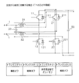
- FIG. 3 is an explanatory diagram showing the operation of each transistor in the positive half cycle of one cycle T1 when the power conversion device of the present embodiment converts from alternating current to direct current.
- the control unit 40 when turning on / off the transistors 11 and 21 (first switching element) in one cycle T1 of alternating current, the transistors 12 and 22 (first circuits) of each series circuit. 2 switching element) is always turned off, and when the transistors 12 and 22 (second switching element) are turned on / off at another period T2 of AC, the transistors 11 and 21 (first switching element) of each series circuit Always turn off to convert AC to DC.
- the alternating current in the positive half cycle of one cycle T1 of alternating current, includes a diode 111 connected in reverse parallel to the transistor 11 of the first series circuit 10, the direct current side, and the second series circuit 20.
- the current flows through a diode 221 connected in reverse parallel to the transistor 22.
- the transistor 21 of the second series circuit 20 When the transistor 21 of the second series circuit 20 is turned on in the positive half cycle of the period T1, it is connected in antiparallel to the transistor 11 of the first series circuit 10 as indicated by the solid line in FIG. A current flows through the diode 111 and the transistor 21 of the second series circuit 20, and electric energy is accumulated in the coils 31 and 32 on the AC side. On the other hand, when the transistor 21 of the second series circuit 20 is turned off, the electrical energy accumulated in the coils 31 and 32 is reversed to the transistor 11 of the first series circuit 10 as indicated by the broken line in FIG. A current flows through the diode 111 connected in parallel and the diode 221 connected in antiparallel to the DC side and the transistor 22 of the second series circuit 20.
- FIG. 4 is an explanatory diagram showing the operation of each transistor in the negative half cycle of one cycle T1 when converting from AC to DC by the power conversion device of the present embodiment.
- the alternating current includes the diode 211 connected in reverse parallel to the transistor 21 of the second series circuit 20, the direct current side, and the first series circuit 10.
- the current flows through a diode 121 connected in reverse parallel to the transistor 12.
- the transistor 11 of the first series circuit 10 When the transistor 11 of the first series circuit 10 is turned on in the negative half cycle of the period T1, it is connected in antiparallel to the transistor 21 of the second series circuit 20 as indicated by the solid line in FIG. A current flows through the diode 211 and the transistor 11 of the first series circuit 10, and electric energy is accumulated in the coils 31 and 32 on the AC side. On the other hand, when the transistor 11 of the first series circuit 10 is turned off, the electrical energy accumulated in the coils 31 and 32 reverses to the transistor 21 of the second series circuit 20 as indicated by the broken line in FIG. Current flows through the diode 211 connected in parallel and the diode 121 connected in antiparallel to the DC side and the transistor 12 of the first series circuit 10.
- FIG. 5 is an explanatory diagram showing the operation of each transistor in the positive half cycle of another cycle T2 when converting from AC to DC by the power conversion device of the present embodiment.
- the AC current is connected to the transistor 111 of the first series circuit 10 in antiparallel, the diode 111, the DC side, and the second series circuit 20.
- the current flows through a diode 221 connected in reverse parallel to the transistor 22.
- FIG. 6 is an explanatory diagram showing the operation of each transistor in the negative half cycle of another cycle T2 when converting from AC to DC by the power conversion device of the present embodiment.
- the AC current is connected in reverse parallel to the transistor 21 of the second series circuit 20, the diode 211, the DC side, and the first series circuit 10.
- the current flows through a diode 121 connected in reverse parallel to the transistor 12.
- the transistor 22 of the second series circuit 20 When the transistor 22 of the second series circuit 20 is turned on in the negative half cycle of the period T2, the transistor 22 and the first series circuit of the second series circuit 20 are indicated by arrows shown by solid lines in FIG. Current flows through the diode 121 connected in antiparallel to the ten transistors 12, and electric energy is stored in the coils 31 and 32 on the AC side. On the other hand, when the transistor 22 of the second series circuit 20 is turned off, the electrical energy accumulated in the coils 31 and 32 reverses to the transistor 21 of the second series circuit 20 as indicated by the broken line in FIG. Current flows through the diode 211 connected in parallel and the diode 121 connected in antiparallel to the DC side and the transistor 12 of the first series circuit 10.
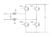
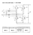
- FIG. 7 is an explanatory diagram showing the configuration of a conventional bridge circuit
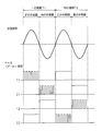
- FIG. 8 is a time chart showing an example of the operating state of each transistor when AC is converted into DC by the conventional bridge circuit.
- the transistors 103 and 104 among the transistors 101, 102, 103, and 104 are the only transistors that repeat the switching operation in each AC cycle. , 102 are always off. For this reason, the switching loss is biased between the transistors, for example, the loss of the transistors 103 and 104 is increased, and the temperature rise is higher than that of the transistors 101 and 102. For this reason, when the operable temperature range of the entire power conversion device is set based on the transistor having the highest temperature rise, as a result, the operable temperature range of the entire device is lowered.
- the bias of transistor loss can be suppressed, the bias related to temperature rise can also be suppressed, and as a result, the operable temperature range of the entire device can be increased. Can do.
- FIG. 9 is a time chart showing an example of the operating state of each transistor when direct current is converted into alternating current by the power conversion device of the present embodiment.
- the upper chart shows the waveform (AC waveform) of the AC voltage such as 50 Hz or 60 Hz
- the lower chart shows the waveform of the base voltage (base waveform) applied to the transistors 11, 21, 12, and 22. Indicates.
- MOSFET MOSFET, it becomes a gate waveform.
- one cycle of the AC waveform is T1
- the next cycle is T2.
- one half cycle of each cycle T1, T2 is a positive half cycle
- the other half cycle is a negative half cycle.
- a time period in which rectangular pulse waveforms are continuous indicates a state in which the transistor is repeatedly turned on / off at a predetermined period.
- the switching frequency of each of the transistors 11, 21, 12, and 22 is, for example, a high frequency of about 50 KHz, which is higher than the AC frequency, but the switching frequency is not limited to 50 kHz.
- the transistor 11 in the positive half cycle of one cycle T1, the transistor 11 is repeatedly turned on / off, the transistors 21 and 12 are always off, and the transistor 22 is always on.
- the transistor 21 is repeatedly turned on / off, the transistors 11 and 22 are always off, and the transistor 12 is always on.
- the transistor 22 is repeatedly turned on / off, the transistors 21 and 12 are always off, and the transistor 11 is always on.
- the transistor 12 is repeatedly turned on / off, the transistors 11 and 22 are always off, and the transistor 21 is always on.
- control unit 40 when the control unit 40 turns on / off the transistor 11 of the first series circuit 10 (one series circuit) in the positive half cycle of the AC cycle T1, the control unit 40 and the transistor 12 of the first series circuit 10 The transistor 12 of the second series circuit 20 (other series circuit) is always turned off, and the transistor 22 of the second series circuit 20 is always turned on.
- control unit 40 turns on / off the transistor 21 of the second series circuit 20 (one series circuit) in the negative half cycle of the AC cycle T1
- the control unit 40 and the transistor 22 of the second series circuit 20 and The transistor 11 of the first column circuit 10 (another series circuit) is always turned off, and the transistor 12 of the first series circuit 10 is always turned on to convert direct current to alternating current.
- control unit 40 when the control unit 40 turns on / off the transistor 22 of the second series circuit 20 (one series circuit) in the positive half cycle of another period T2 of AC, the control unit 40 and the transistor 21 of the second series circuit 20 and the second series circuit 20 The transistor 12 of the first series circuit 10 (other series circuit) is always turned off, and the transistor 11 of the first series circuit 10 is always turned on.
- control unit 40 turns on / off the transistor 12 of the first series circuit 10 (one series circuit) in the negative half cycle of the other period T2 of AC
- control unit 40 and the transistor 11 of the first series circuit 10 and The transistor 22 of the second series circuit 20 is always turned off, and the transistor 21 of the second series circuit 20 is always turned on to convert direct current into alternating current.
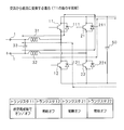
- FIG. 10 is an explanatory diagram showing the operation of each transistor in the positive half cycle of one cycle T1 when converting from direct current to alternating current by the power conversion device of the present embodiment.
- the transistor 11 of the first series circuit 10 is turned on / off, and the transistor 12 of the first series circuit 10 and the transistor of the second series circuit 20 are turned on. 21 is always off, and the transistor 22 of the second series circuit 20 is always on.
- the transistor 11 of the first series circuit 10 when the transistor 11 of the first series circuit 10 is turned on in the positive half cycle of the period T1, the transistor 11, the coil 31, and the alternating current of the first series circuit 10 as indicated by the solid line in FIG. A current flows through the side and the transistor 22 of the second series circuit 20.
- the transistor 11 of the first series circuit 10 when the transistor 11 of the first series circuit 10 is turned off, currents in the same direction flow through the coils 31 and 32 as indicated by the broken lines in FIG. A current flows through the diode 121, the coil 31, the AC side, and the transistor 22 of the second series circuit 20 connected in antiparallel to the transistor 12.
- FIG. 11 is an explanatory diagram showing the operation of each transistor in the negative half cycle of one cycle T1 when converting from direct current to alternating current by the power conversion device of the present embodiment.
- the transistor 21 of the second series circuit 20 is turned on / off, and the transistor 22 of the second series circuit 20 and the transistor of the first series circuit 10 are turned on.
- 11 is always off, and the transistor 12 of the first series circuit 10 is always on.
- FIG. 12 is an explanatory diagram showing the operation of each transistor in the positive half cycle of another cycle T2 when converting from direct current to alternating current by the power conversion device of the present embodiment.
- the transistor 22 of the second series circuit 20 is turned on / off, and the transistor 21 of the second series circuit 20 and the transistor of the first series circuit 10 are turned on. 12 is always off, and the transistor 11 of the first series circuit 10 is always on.
- the transistor 22 of the second series circuit 20 when the transistor 22 of the second series circuit 20 is turned on in the positive half cycle of the period T2, the transistor 11, the coil 31, and the alternating current of the first series circuit 10 as indicated by the solid line in FIG. A current flows through the side and the transistor 22 of the second series circuit 20.
- the transistor 22 of the second series circuit 20 when the transistor 22 of the second series circuit 20 is turned off, currents in the same direction are caused to flow through the coils 31 and 32 as indicated by the broken lines in FIG. A current flows through the transistor 211, the coil 31, the AC side, and the diode 211 connected in antiparallel to the transistor 21 of the second series circuit 20.
- FIG. 13 is an explanatory diagram showing the operation of each transistor in the negative half cycle of another cycle T2 when converting from direct current to alternating current by the power conversion device of the present embodiment.
- the transistor 12 of the first series circuit 10 is turned on / off, and the transistor 11 of the first series circuit 10 and the transistor 22 of the second series circuit 20 are always turned off.
- the transistor 21 of the second series circuit 20 is always turned on.
- FIG. 14 is a time chart showing an example of an operation state of each transistor when a direct current is converted into an alternating current by a conventional bridge circuit.
- the configuration of the conventional bridge circuit is the same as that in FIG.
- the transistors 101, 102, and 104 are the only transistors that repeat the switching operation in each AC cycle. 104 are always off or always on. For this reason, the switching loss is biased between the transistors, for example, the loss of the transistors 101 and 102 is increased, and the temperature rise is higher than that of the transistors 103 and 104. For this reason, when the operable temperature range of the entire power conversion device is set based on the transistor having the highest temperature rise, as a result, the operable temperature range of the entire device is lowered.
- the bias of transistor loss can be suppressed, the bias related to temperature rise can also be suppressed, and as a result, the operable temperature range of the entire device can be increased. Can do.
- the transistor 21 when the transistor 21 repeats on / off in the positive half cycle of the AC cycle T1, the other transistors 11, 12, and 22 Although it is always off, it is not limited to such a configuration.
- the transistor 22 when the transistor 21 is repeatedly turned on / off, the transistor 22 may be turned on when the transistor 21 is turned off.
- the transistor 11 when the transistor 11 repeats ON / OFF in the negative half cycle of the AC cycle T1, the other transistors 11, 12, and 22 are always off.
- the present invention is not limited to this configuration. Absent.
- the transistor 11 when the transistor 11 is repeatedly turned on / off, the transistor 12 may be turned on when the transistor 11 is turned off.
- the transistor 21 of the second series circuit 20 (one series circuit) is turned on / off in the positive half cycle of the AC cycle T1
- the transistor 22 of the second series circuit 20 can be turned on.
- control unit 40 turns on / off the transistor 11 of the first series circuit 10 (one series circuit).
- the first series circuit 10 The transistor 12 can be turned on.
- the control unit 40 when the transistor 12 of the first series circuit 10 (one series circuit) is turned on / off in the positive half cycle of the other cycle T2 of AC, the control unit 40 is in the off state.
- the transistor 11 of the first series circuit 10 can be turned on.
- control unit 40 turns on / off the transistor 22 of the second series circuit 10 (one series circuit), and when the transistor 222 is in the off state, the second series circuit 20
- the transistor 21 can be turned on.
- control unit 40 turns on the transistors 11, 21, 12, and 22 so that one cycle T1 of alternating current and another cycle T2 are alternately repeated (for example, as shown in FIGS. 2 and 9). Can be turned off. Thereby, the time width (period) during which the transistors 11, 21, 12, and 22 of each series circuit are turned on / off can be equalized, and the bias of the switching loss of each of the transistors 11, 21, 12, and 22 is suppressed. be able to.
- FIG. 15 is a time chart showing another example of the operation state of each transistor when AC is converted into DC by the power conversion device of the present embodiment. The same applies when converting direct current to alternating current.
- the control unit 40 includes a first time width in which a cycle (period T1) in which the transistors 11 and 21 repeat ON / OFF is repeated a plurality of times, and the transistors 12 and 22 are turned ON / OFF The transistors 11, 21, 12, and 22 are turned on / off so that the second time width in which the cycle of repeating (cycle T2) is repeated a plurality of times is alternately repeated.
- the transistors 11, 21, 12, and 22 of each series circuit are The ON / OFF time width (period) can be made uniform, and the bias of the switching losses of the transistors 11, 21, 12, and 22 can be suppressed.
- control unit 40 can change the ratio of the first time width and the second time width described above according to the thermal resistance of the transistors 11 and 21 and the thermal resistance of the transistors 12 and 22.
- the control unit 40 can change the ratio of the first time width and the second time width described above according to the thermal resistance of the transistors 11 and 21 and the thermal resistance of the transistors 12 and 22.
- the transistors are longer than the first time width for turning on / off the transistors 11 and 21
- the switching loss of the transistors 12 and 22 is made smaller than the switching loss of the transistors 11 and 21 by shortening the second time width during which the transistors 12 and 22 are turned on / off. The uneven temperature rise can be suppressed.
Landscapes
- Engineering & Computer Science (AREA)
- Power Engineering (AREA)
- Inverter Devices (AREA)
- Rectifiers (AREA)
Abstract
電力変換装置は、第1のスイッチング素子及び第2のスイッチング素子それぞれに逆並列に接続されたダイオードと、第1のスイッチング素子及び第2のスイッチング素子を交流周期よりも短い所定周期でオン/オフする制御部とを備え、制御部は、交流の一の周期の一方の半周期で一方の直列回路の第1のスイッチング素子をオン/オフし、他方の半周期で他方の直列回路の第1のスイッチング素子をオン/オフするようにしてあり、さらに、一の周期と異なる他の周期の一方の半周期で一方の直列回路の第2のスイッチング素子をオン/オフし、他方の半周期で他方の直列回路の第2のスイッチング素子をオン/オフするようにしてある。
Description
本発明は、電力変換装置に関する。
本出願は、2015年6月1日出願の日本出願第2015-111543号に基づく優先権を主張し、前記日本出願に記載された全ての記載内容を援用するものである。
本出願は、2015年6月1日出願の日本出願第2015-111543号に基づく優先権を主張し、前記日本出願に記載された全ての記載内容を援用するものである。
近年、バッテリの充電時には外部から入力される交流を直流に変換し、交流電力を出力する場合には、バッテリからの直流を交流に変換する双方向の電力変換装置が注目されている。例えば、2つのスイッチング素子を直列に接続した直列回路を複数備え、当該直列回路を並列に接続した双方向DC/ACインバータが開示されている(特許文献1参照)。
本開示の電力変換装置は、第1のスイッチング素子及び第2のスイッチング素子を直列に接続した直列回路を複数備え、各直列回路を並列に接続してあり、各直列回路の一端及び他端それぞれを直流側の正側及び負側としてあり、前記第1のスイッチング素子及び第2のスイッチング素子の接続点それぞれに一端を接続したフィルタ回路をさらに備え、該フィルタ回路の他端を交流側とした電力変換装置であって、前記第1のスイッチング素子及び第2のスイッチング素子それぞれに逆並列に接続されたダイオードと、前記第1のスイッチング素子及び第2のスイッチング素子を交流周期よりも短い所定周期でオン/オフする制御部とを備え、該制御部は、交流の一の周期の一方の半周期で一方の直列回路の第1のスイッチング素子をオン/オフし、他方の半周期で他方の直列回路の第1のスイッチング素子をオン/オフするようにしてあり、さらに、前記一の周期と異なる他の周期の一方の半周期で一方の直列回路の第2のスイッチング素子をオン/オフし、他方の半周期で他方の直列回路の第2のスイッチング素子をオン/オフするようにしてある。
[本開示が解決しようとする課題]
特許文献1の装置にあっては、直流と交流との間で双方向に変換する場合、それぞれの直列回路の一方のスイッチング素子だけをオン/オフさせているため、スイッチング損失に偏りが生じ、その結果としてスイッチング素子の温度上昇に偏りが生ずるという問題がある。
特許文献1の装置にあっては、直流と交流との間で双方向に変換する場合、それぞれの直列回路の一方のスイッチング素子だけをオン/オフさせているため、スイッチング損失に偏りが生じ、その結果としてスイッチング素子の温度上昇に偏りが生ずるという問題がある。
そこで、スイッチング素子の損失の偏りを抑制することができる電力変換装置を提供することを目的とする。
[本開示の効果]
[本開示の効果]
本開示によれば、スイッチング素子の損失の偏りを抑制することができる。
[本願発明の実施形態の説明]
本実施の形態に係る電力変換装置は、第1のスイッチング素子及び第2のスイッチング素子を直列に接続した直列回路を複数備え、各直列回路を並列に接続してあり、各直列回路の一端及び他端それぞれを直流側の正側及び負側としてあり、前記第1のスイッチング素子及び第2のスイッチング素子の接続点それぞれに一端を接続したフィルタ回路をさらに備え、該フィルタ回路の他端を交流側とした電力変換装置であって、前記第1のスイッチング素子及び第2のスイッチング素子それぞれに逆並列に接続されたダイオードと、前記第1のスイッチング素子及び第2のスイッチング素子を交流周期よりも短い所定周期でオン/オフする制御部とを備え、該制御部は、交流の一の周期の一方の半周期で一方の直列回路の第1のスイッチング素子をオン/オフし、他方の半周期で他方の直列回路の第1のスイッチング素子をオン/オフするようにしてあり、さらに、前記一の周期と異なる他の周期の一方の半周期で一方の直列回路の第2のスイッチング素子をオン/オフし、他方の半周期で他方の直列回路の第2のスイッチング素子をオン/オフするようにしてある。
本実施の形態に係る電力変換装置は、第1のスイッチング素子及び第2のスイッチング素子を直列に接続した直列回路を複数備え、各直列回路を並列に接続してあり、各直列回路の一端及び他端それぞれを直流側の正側及び負側としてあり、前記第1のスイッチング素子及び第2のスイッチング素子の接続点それぞれに一端を接続したフィルタ回路をさらに備え、該フィルタ回路の他端を交流側とした電力変換装置であって、前記第1のスイッチング素子及び第2のスイッチング素子それぞれに逆並列に接続されたダイオードと、前記第1のスイッチング素子及び第2のスイッチング素子を交流周期よりも短い所定周期でオン/オフする制御部とを備え、該制御部は、交流の一の周期の一方の半周期で一方の直列回路の第1のスイッチング素子をオン/オフし、他方の半周期で他方の直列回路の第1のスイッチング素子をオン/オフするようにしてあり、さらに、前記一の周期と異なる他の周期の一方の半周期で一方の直列回路の第2のスイッチング素子をオン/オフし、他方の半周期で他方の直列回路の第2のスイッチング素子をオン/オフするようにしてある。
電力変換装置は、第1のスイッチング素子及び第2のスイッチング素子を直列に接続した直列回路を複数備え、各直列回路を並列に接続してあり、各直列回路の一端及び他端それぞれを直流側の正側及び負側としてあり、第1のスイッチング素子及び第2のスイッチング素子の接続点それぞれに一端を接続したフィルタ回路をさらに備え、フィルタ回路の他端を交流側としてある。すなわち、各直列回路の第1のスイッチング素子及び第2のスイッチング素子によりブリッジ回路を構成してある。フィルタ回路は、例えば、キャパシタ及び複数のコイルで構成され、各コイルの一端を第1のスイッチング素子及び第2のスイッチング素子の接続点それぞれに接続し、コイルの他端を交流側とすることができる。また、各コイルの他端間にキャパシタを接続することができる。
第1のスイッチング素子及び第2のスイッチング素子それぞれに逆並列に接続されたダイオードを備える。例えば、スイッチング素子がトランジスタである場合、各トランジスタのコレクタ・エミッタ間に逆並列にダイオードを接続してある。
制御部は、第1のスイッチング素子及び第2のスイッチング素子を交流周期よりも短い所定周期でオン/オフする。交流周期は、例えば、商用周波数(50Hz、60Hz)に対応する周期である。所定周期は、高周波数(例えば、50KHz)に対応する周期である。
制御部は、交流の一の周期の一方の半周期で一方の直列回路の第1のスイッチング素子をオン/オフし、他方の半周期で他方の直列回路の第1のスイッチング素子をオン/オフする。また、制御部は、一の周期と異なる他の周期(例えば、一の周期の次の周期)の一方の半周期で一方の直列回路の第2のスイッチング素子をオン/オフし、他方の半周期で他方の直列回路の第2のスイッチング素子をオン/オフする。交流の一の周期及び他の周期に亘る時間幅においては、交流の1周期毎に、第1のスイッチング素子及び第2のスイッチング素子のうちの異なるスイッチング素子が順番に繰り返しオン/オフするので、各スイッチング素子のスイッチング損失の偏りを抑制することができる。
本実施の形態に係る電力変換装置は、前記制御部は、前記一の周期で前記第1のスイッチング素子をオン/オフする場合、各直列回路の第2のスイッチング素子を常時オフにし、前記他の周期で前記第2のスイッチング素子をオン/オフする場合、各直列回路の第1のスイッチング素子を常時オフにし、交流を直流に変換するようにしてある。
制御部は、交流の一の周期で第1のスイッチング素子をオン/オフする場合、各直列回路の第2のスイッチング素子を常時オフにし、交流の他の周期で第2のスイッチング素子をオン/オフする場合、各直列回路の第1のスイッチング素子を常時オフにして交流を直流に変換する。並列接続された直列回路を、第1直列回路、第2直列回路とする。
交流の一の周期の一方の半周期(例えば、正の半周期)では、交流電流は、第1直列回路の第1スイッチング素子に逆並列に接続されたダイオード、直流側及び第2直列回路の第2のスイッチング素子に逆並列に接続されたダイオードを流れる。そして、交流の一の周期の一方の半周期において、第2直列回路の第1のスイッチング素子をオンした場合には、第1直列回路の第1のスイッチング素子に逆並列に接続されたダイオード及び第2直列回路の第1のスイッチング素子を通じて電流が流れ、交流側のコイルに電気エネルギーが蓄積される。一方、交流の一の周期の一方の半周期において、第2直列回路の第1のスイッチング素子をオフした場合には、コイルに蓄積された電気エネルギーにより、第1直列回路の第1のスイッチング素子に逆並列に接続されたダイオード、直流側及び第2直列回路の第2のスイッチング素子に逆並列に接続されたダイオードに電流が流れる。
同様に、交流の一の周期の他方の半周期(例えば、負の半周期)では、交流電流は、第2直列回路の第1のスイッチング素子に逆並列に接続されたダイオード、直流側及び第1直列回路の第2のスイッチング素子に逆並列に接続されたダイオードを流れる。そして、交流の一の周期の他方の半周期において、第1直列回路の第1のスイッチング素子をオンした場合には、第2直列回路の第1のスイッチング素子に逆並列に接続されたダイオード及び第1直列回路の第1のスイッチング素子を通じて電流が流れ、交流側のコイルに電気エネルギーが蓄積される。一方、交流の一の周期の他方の半周期において、第1直列回路の第1のスイッチング素子をオフした場合には、コイルに蓄積された電気エネルギーにより、第2直列回路の第1のスイッチング素子に逆並列に接続されたダイオード、直流側及び第1直列回路の第2のスイッチング素子に逆並列に接続されたダイオードに電流が流れる。
同様に、交流の他の周期の一方の半周期(例えば、正の半周期)では、交流電流は、第1直列回路の第1スイッチング素子に逆並列に接続されたダイオード、直流側及び第2直列回路の第2のスイッチング素子に逆並列に接続されたダイオードを流れる。そして、交流の他の周期の一方の半周期において、第1直列回路の第2のスイッチング素子をオンした場合には、第1直列回路の第2のスイッチング素子及び第2直列回路の第2のスイッチング素子に逆並列に接続されたダイオードを通じて電流が流れ、交流側のコイルに電気エネルギーが蓄積される。一方、交流の他の周期の一方の半周期において、第1直列回路の第2のスイッチング素子をオフした場合には、コイルに蓄積された電気エネルギーにより、第1直列回路の第1のスイッチング素子に逆並列に接続されたダイオード、直流側及び第2直列回路の第2のスイッチング素子に逆並列に接続されたダイオードに電流が流れる。
同様に、交流の他の周期の他方の半周期(例えば、負の半周期)では、交流電流は、第2直列回路の第1のスイッチング素子に逆並列に接続されたダイオード、直流側及び第1直列回路の第2のスイッチング素子に逆並列に接続されたダイオードを流れる。そして、交流の他の周期の他方の半周期において、第2直列回路の第2のスイッチング素子をオンした場合には、第2直列回路の第2のスイッチング素子及び第1直列回路の第2のスイッチング素子に逆並列に接続されたダイオードを通じて電流が流れ、交流側のコイルに電気エネルギーが蓄積される。一方、交流の他の周期の他方の半周期において、第2直列回路の第2のスイッチング素子をオフした場合には、コイルに蓄積された電気エネルギーにより、第2直列回路の第1のスイッチング素子に逆並列に接続されたダイオード、直流側及び第1直列回路の第2のスイッチング素子に逆並列に接続されたダイオードに電流が流れる。
本実施の形態に係る電力変換装置は、前記制御部は、前記一の周期で一の直列回路の第1のスイッチング素子をオン/オフする場合、該一の直列回路の第2のスイッチング素子及び他の直列回路の第1のスイッチング素子を常時オフにし、前記他の直列回路の第2のスイッチング素子を常時オンにし、前記他の周期で一の直列回路の第2スイッチング素子をオン/オフする場合、該一の直列回路の第1のスイッチング素子及び他の直列回路の第2のスイッチング素子を常時オフにし、前記他の直列回路の第1のスイッチング素子を常時オンにし、直流を交流に変換するようにしてある。
制御部は、交流の一の周期で一の直列回路の第1のスイッチング素子をオン/オフする場合、一の直列回路の第2のスイッチング素子及び他の直列回路の第1のスイッチング素子を常時オフにし、他の直列回路の第2のスイッチング素子を常時オンにし、また、交流の他の周期で一の直列回路の第2スイッチング素子をオン/オフする場合、一の直列回路の第1のスイッチング素子及び他の直列回路の第2のスイッチング素子を常時オフにし、他の直列回路の第1のスイッチング素子を常時オンにし、直流を交流に変換する。並列接続された直列回路を、第1直列回路、第2直列回路とする。
交流の一の周期の一方の半周期(例えば、正の半周期)では、第1直列回路の第1のスイッチング素子をオン/オフし、第1直列回路の第2のスイッチング素子及び第2直列回路の第1のスイッチング素子を常時オフにし、第2直列回路の第2のスイッチング素子を常時オンにする。すなわち、交流の一の周期の一方の半周期において、第1直列回路の第1のスイッチング素子をオンした場合には、第1直列回路の第1のスイッチング素子、コイル、交流側及び第2直列回路の第2のスイッチング素子に電流が流れる。一方、交流の一の周期の一方の半周期において、第1直列回路の第1のスイッチング素子をオフした場合には、コイルに同じ向きの電流を流そうとするので、第1直列回路の第2のスイッチング素子に逆並列に接続されたダイオード、コイル、交流側及び第2直列回路の第2のスイッチング素子に電流が流れる。
同様に、交流の一の周期の他方の半周期(例えば、負の半周期)では、第2直列回路の第1のスイッチング素子をオン/オフし、第2直列回路の第2のスイッチング素子及び第1直列回路の第1のスイッチング素子を常時オフにし、第1直列回路の第2のスイッチング素子を常時オンにする。すなわち、交流の一の周期の他方の半周期において、第2直列回路の第1のスイッチング素子をオンした場合には、第2直列回路の第1のスイッチング素子、コイル、交流側及び第1直列回路の第2のスイッチング素子に電流が流れる。一方、交流の一の周期の他方の半周期において、第2直列回路の第1のスイッチング素子をオフした場合には、コイルに同じ向きの電流を流そうとするので、第2直列回路の第2のスイッチング素子に逆並列に接続されたダイオード、コイル、交流側及び第1直列回路の第2のスイッチング素子に電流が流れる。これにより、直流を交流に変換することができる。
同様に、交流の他の周期の一方の半周期(例えば、正の半周期)では、第2直列回路の第2のスイッチング素子をオン/オフし、第2直列回路の第1のスイッチング素子及び第1直列回路の第2のスイッチング素子を常時オフにし、第1直列回路の第1のスイッチング素子を常時オンにする。すなわち、交流の他の周期の一方の半周期において、第2直列回路の第2のスイッチング素子をオンした場合には、第1直列回路の第1のスイッチング素子、コイル、交流側及び第2直列回路の第2のスイッチング素子に電流が流れる。一方、交流の他の周期の一方の半周期において、第2直列回路の第2のスイッチング素子をオフした場合には、コイルに同じ向きの電流を流そうとするので、第1直列回路の第1のスイッチング素子、コイル、交流側及び第2直列回路の第1のスイッチング素子に逆並列に接続されたダイオードに電流が流れる。
同様に、交流の他の周期の他方の半周期(例えば、負の半周期)では、第1直列回路の第2のスイッチング素子をオン/オフし、第1直列回路の第1のスイッチング素子及び第2直列回路の第2のスイッチング素子を常時オフにし、第2直列回路の第1のスイッチング素子を常時オンにする。すなわち、交流の他の周期の他方の半周期において、第1直列回路の第2のスイッチング素子をオンした場合には、第2直列回路の第1のスイッチング素子、コイル、交流側及び第1直列回路の第2のスイッチング素子に電流が流れる。一方、交流の他の周期の他方の半周期において、第1直列回路の第2のスイッチング素子をオフした場合には、コイルに同じ向きの電流を流そうとするので、第1直列回路の第1のスイッチング素子に逆並列に接続されたダイオード、第2直列回路の第1のスイッチング素子、コイル、交流側に電流が流れる。これにより、直流を交流に変換することができる。
本実施の形態に係る電力変換装置は、前記制御部は、一の直列回路の第1のスイッチング素子をオン/オフする場合、該第1のスイッチング素子がオフ状態のときに該直列回路の第2のスイッチング素子をオン状態にし、一の直列回路の第2のスイッチング素子をオン/オフする場合、該第2のスイッチング素子がオフ状態のときに該直列回路の第1のスイッチング素子をオン状態にするようにしてある。
制御部は、一の直列回路の第1のスイッチング素子をオン/オフする場合、当該第1のスイッチング素子がオフ状態のときに当該直列回路の第2のスイッチング素子をオン状態にし、一の直列回路の第2のスイッチング素子をオン/オフする場合、当該第2のスイッチング素子がオフ状態のときに当該直列回路の第1のスイッチング素子をオン状態にする。
例えば、交流の一の周期の一方の半周期(例えば、正の半周期)において、第2直列回路の第1のスイッチング素子をオン/オフする場合に、第2直列回路の第1のスイッチング素子がオフの状態であるとき、第2直列回路の第2のスイッチング素子をオン状態にする。交流の一の周期の一方の半周期において、第2直列回路の第1のスイッチング素子をオフした場合には、第2直列回路の第1のスイッチング素子がオン状態のときに流れる電流に基づいてコイルに蓄積された電気エネルギーにより、第1直列回路の第1のスイッチング素子に逆並列に接続されたダイオード、直流側及び第2直列回路の第2のスイッチング素子に逆並列に接続されたダイオードに電流が流れる。すなわち、第2直列回路の第2のスイッチング素子(例えば、FET)と該第2のスイッチング素子に逆並列に接続されたダイオードの両方に電流を流す(同期整流とも称する)ことにより、電流を分配して各素子に流れる電流を少なくすることができる。
本実施の形態に係る電力変換装置は、前記制御部は、前記一の周期と他の周期とが交互に繰り返されるように前記第1のスイッチング素子及び第2のスイッチング素子をオン/オフするようにしてある。
制御部は、交流の一の周期と他の周期とが交互に繰り返されるように第1のスイッチング素子及び第2のスイッチング素子をオン/オフする。これにより、各直列回路の第1のスイッチング素子及び第2のスイッチング素子がオン/オフする時間幅(期間)を均等にすることができ、第1のスイッチング素子及び第2のスイッチング素子それぞれのスイッチング損失の偏りを抑制することができる。
本実施の形態に係る電力変換装置は、前記制御部は、前記一の周期を連続して複数回繰り返した第1の時間幅と前記他の周期を連続して複数回繰り返した第2の時間幅とが交互に繰り返されるように前記第1のスイッチング素子及び第2のスイッチング素子をオン/オフするようにしてある。
制御部は、交流の一の周期を連続して複数回繰り返した第1の時間幅と他の周期を連続して複数回繰り返した第2の時間幅とが交互に繰り返されるように第1のスイッチング素子及び第2のスイッチング素子をオン/オフする。第1の時間幅と第2の時間幅とを同じ時間幅にすれば、各直列回路の第1のスイッチング素子及び第2のスイッチング素子がオン/オフする時間幅(期間)を均等にすることができ、第1のスイッチング素子及び第2のスイッチング素子それぞれのスイッチング損失の偏りを抑制することができる。
本実施の形態に係る電力変換装置は、前記制御部は、前記第1のスイッチンング素子及び前記第2のスイッチング素子それぞれの熱抵抗の大小に応じて、前記第1の時間幅及び前記第2の時間幅の割合を変更するようにしてある。
制御部は、第1のスイッチンング素子及び第2のスイッチング素子それぞれの熱抵抗の大小に応じて、第1の時間幅及び第2の時間幅の割合を変更する。スイッチング素子の実装状態などに応じて、例えば、第1のスイッチング素子の熱抵抗が第2のスイッチング素子の熱抵抗よりも小さい場合には、第1のスイッチング素子をオン/オフする第1の時間幅よりも第2のスイッチング素子をオン/オフする第2の時間幅を短くすることにより、第2のスイッチング素子のスイッチング損失を第1のスイッチング素子のスイッチング損失よりも小さくして、各スイッチング素子の温度上昇の偏りを抑制することができる。
[本願発明の実施形態の詳細]
以下、本発明を実施の形態を示す図面に基づいて説明する。図1は本実施の形態の電力変換装置の回路構成の一例を示す説明図である。本実施の形態の電力変換装置は、交流側の端子1、直流側の端子2、第1直列回路10、第2直列回路20、フィルタ回路30、制御部40、平滑用のキャパシタ50、DC/DCコンバータ60などを備える。電力変換装置は、交流側の端子1に商用電源(50Hz、60Hzなどの商用周波数の電源)を接続して交流電力を供給した場合、交流を直流に変換することにより、直流側の端子2から所要の電圧の直流電力を出力し、例えば、バッテリ3を充電することができる。また、直流側の端子2にバッテリ3などの直流電源を接続して直流電力を供給した場合、直流を交流に変換することにより、交流側の端子1から交流電力を出力することができる。
以下、本発明を実施の形態を示す図面に基づいて説明する。図1は本実施の形態の電力変換装置の回路構成の一例を示す説明図である。本実施の形態の電力変換装置は、交流側の端子1、直流側の端子2、第1直列回路10、第2直列回路20、フィルタ回路30、制御部40、平滑用のキャパシタ50、DC/DCコンバータ60などを備える。電力変換装置は、交流側の端子1に商用電源(50Hz、60Hzなどの商用周波数の電源)を接続して交流電力を供給した場合、交流を直流に変換することにより、直流側の端子2から所要の電圧の直流電力を出力し、例えば、バッテリ3を充電することができる。また、直流側の端子2にバッテリ3などの直流電源を接続して直流電力を供給した場合、直流を交流に変換することにより、交流側の端子1から交流電力を出力することができる。
第1直列回路10は、第1のスイッチング素子としてのバイポーラトランジスタ11及び第2のスイッチング素子としてのバイポーラトランジスタ12を直列に接続した構成を有する。バイポーラトランジスタ11は、例えば、IGBT(Insulated Gate Bipolar Transistor)を用いることができる。なお、以下の説明では、簡便のため、バイポーラトランジスタを単にトランジスタと称する。第1直列回路10は、トランジスタ11のエミッタとトランジスタ12のコレクタとを接続してある。
同様に、第2直列回路20は、第1のスイッチング素子としてのトランジスタ21及び第2のスイッチング素子としてのトランジスタ22を直列に接続した構成を有する。第2直列回路20は、トランジスタ21のエミッタとトランジスタ22のコレクタとを接続してある。なお、IGBTに代えて、MOSFET(Metal Oxide Semiconductor Field Effect Transistor)を用いることもできる。
第1直列回路10及び第2直列回路20は並列に接続してある。すなわち、トランジスタ11、21それぞれのコレクタを直流側の正側の電路4に接続するとともに、トランジスタ12、22それぞれのエミッタを直流側の負側(例えば、接地レベル)の電路5に接続してある。これにより、トランジスタ11、12、21、22により、いわゆるブリッジ回路を構成している。また、電路4、5の間には、平滑用のキャパシタ50を接続してある。なお、以下、第1直列回路10及び第2直列回路20を纏めてブリッジ回路とも称する。
トランジスタ11、12、21、22それぞれのコレクタ・エミッタ間には、ダイオード(例えば、FRD:ファーストリカバリーダイオード)111、121、211、221を逆並列に接続してある。すなわち、各ダイオードのアノードをトランジスタのエミッタに接続し、カソードをコレクタに接続してある。なお、ダイオードは、トランジスタに内蔵されるものでもよく、外付けのものでもよい。
フィルタ回路30は、コイル31、32、キャパシタ33などを備える。コイル31の一端は、トランジスタ11のエミッタとトランジスタ12のコレクタとの接続点に接続してあり、コイル31の他端は、交流側の一方の端子1に接続してある。また、コイル32の一端は、トランジスタ21のエミッタとトランジスタ22のコレクタとの接続点に接続してあり、コイル32の他端は、交流側の他方の端子1に接続してある。コイル31、32の他端の間にはキャパシタ33を接続してある。
制御部40は、トランジスタ11、12、21、22のスイッチングを制御する。具体的には、制御部40の出力端は、トランジスタ11、12、21、22それぞれのベースに接続してあり、制御部40は、ベース信号を出力端から出力する。
DC/DCコンバータ60は、直流電圧を昇圧及び降圧する機能を備える。
トランジスタ11、12、21、22は、いわゆる少数キャリアを電気伝導に使用する少数キャリアデバイスであり、一般的に順方向にバイアスされた状態でのスイッチング損失が多く、寄生ダイオードがなく、逆方向にバイアスされた状態でのスイッチング損失が少ない。
次に、本実施の形態の電力変換装置の動作について説明する。前述のとおり、本実施の形態の電力変換装置は、交流を直流に変換する(PFC制御ともいう)ことができるとともに、直流を交流に変換する(インバータ制御ともいう)ことができる。まず、交流を直流に変換する場合について説明する。
図2は本実施の形態の電力変換装置による交流を直流に変換する場合の各トランジスタの動作状態の一例を示すタイムチャートである。図2中、上段のチャートは、商用電源(50Hz、60Hzなど)の交流電圧の波形(交流波形)を示し、下段のチャートは、トランジスタ11、21、12、22へ印加されるベース電圧の波形(ベース波形)を示す。なお、MOSFETを用いる場合には、ゲート波形となる。図2に示すように、交流波形の一の周期をT1とし、次の周期をT2とする。また、各周期T1、T2の一方の半周期を正の半周期とし、他方の半周期を負の半周期とする。また、ベース波形のうち、矩形状のパルス波形が連続している時間帯は、トランジスタが所定周期でオン/オフを繰り返している状態を示す。各トランジスタ11、21、12、22のスイッチング周波数は、例えば、交流周波数よりも高い、50KHz程度の高周波であるが、スイッチング周波数は、50kHzに限定されるものではない。
図2の例では、一の周期T1の正の半周期では、トランジスタ21がオン/オフを繰り返し、他のトランジスタ11、12、22は常時オフとなっている。また、一の周期T1の負の半周期では、トランジスタ11がオン/オフを繰り返し、他のトランジスタ21、12、22は常時オフとなっている。また、他の周期T2の正の半周期では、トランジスタ12がオン/オフを繰り返し、他のトランジスタ11、21、22は常時オフとなっている。また、他の周期T2の負の半周期では、トランジスタ22がオン/オフを繰り返し、他のトランジスタ11、21、12は常時オフとなっている。
すなわち、制御部40は、トランジスタ11、21、12、22を交流周期よりも短い所定周期でオン/オフする。交流周期は、例えば、商用周波数(50Hz、60Hz)に対応する周期である。所定周期は、高周波数(例えば、50KHz)に対応する周期である。
制御部40は、交流の一の周期T1の一方の半周期(正の半周期)で第2直列回路20(一方の直列回路)のトランジスタ21をオン/オフし、他方の半周期(負の半周期)で第1直列回路10(他方の直列回路)のトランジスタ11をオン/オフする。
また、制御部40は、一の周期と異なる他の周期T2の一方の半周期(正の半周期)で第1直列回路10(一方の直列回路)のトランジスタ12をオン/オフし、他方の半周期(負の半周期)で第2直列回路20(他方の直列回路)のトランジスタ22をオン/オフする。
交流の一の周期T1及び他の周期T2に亘る時間幅においては、交流の1周期毎に、トランジスタ11、21、12、22のうちの異なるトランジスタが順番に繰り返しオン/オフするので、各トランジスタ11、21、12、22のスイッチング損失の偏りを抑制することができる。
次に、交流の一の周期T1及び他の周期T2における動作について具体的に説明する。図3は本実施の形態の電力変換装置により交流から直流に変換する場合の一の周期T1の正の半周期における各トランジスタの動作を示す説明図である。前述のとおり(図2を参照)、制御部40は、交流の一の周期T1でトランジスタ11、21(第1のスイッチング素子)をオン/オフする場合、各直列回路のトランジスタ12、22(第2のスイッチング素子)を常時オフにし、交流の他の周期T2でトランジスタ12、22(第2のスイッチング素子)をオン/オフする場合、各直列回路のトランジスタ11、21(第1のスイッチング素子)を常時オフにして交流を直流に変換する。
図3に示すように、交流の一の周期T1の正の半周期では、交流電流は、第1直列回路10のトランジスタ11に逆並列に接続されたダイオード111、直流側及び第2直列回路20のトランジシタ22に逆並列に接続されたダイオード221を流れる。
そして、周期T1の正の半周期において、第2直列回路20のトランジスタ21をオンした場合には、図3中実線で示す矢印のように、第1直列回路10のトランジスタ11に逆並列に接続されたダイオード111及び第2直列回路20のトランジスタ21を通じて電流が流れ、交流側のコイル31、32に電気エネルギーが蓄積される。一方、第2直列回路20のトランジスタ21をオフした場合には、図3中破線で示す矢印のように、コイル31、32に蓄積された電気エネルギーにより、第1直列回路10のトランジスタ11に逆並列に接続されたダイオード111、直流側及び第2直列回路20のトランジスタ22に逆並列に接続されたダイオード221に電流が流れる。
図4は本実施の形態の電力変換装置により交流から直流に変換する場合の一の周期T1の負の半周期における各トランジスタの動作を示す説明図である。図4に示すように、交流の一の周期T1の負の半周期では、交流電流は、第2直列回路20のトランジスタ21に逆並列に接続されたダイオード211、直流側及び第1直列回路10のトランジスタ12に逆並列に接続されたダイオード121を流れる。
そして、周期T1の負の半周期において、第1直列回路10のトランジスタ11をオンした場合には、図4中実線で示す矢印のように、第2直列回路20のトランジスタ21に逆並列に接続されたダイオード211及び第1直列回路10のトランジスタ11を通じて電流が流れ、交流側のコイル31、32に電気エネルギーが蓄積される。一方、第1直列回路10のトランジスタ11をオフした場合には、図4中破線で示す矢印のように、コイル31、32に蓄積された電気エネルギーにより、第2直列回路20のトランジスタ21に逆並列に接続されたダイオード211、直流側及び第1直列回路10のトランジスタ12に逆並列に接続されたダイオード121に電流が流れる。
図5は本実施の形態の電力変換装置により交流から直流に変換する場合の他の周期T2の正の半周期における各トランジスタの動作を示す説明図である。図5に示すように、交流の他の周期T2の正の半周期では、交流電流は、第1直列回路10のトランジスタ11に逆並列に接続されたダイオード111、直流側及び第2直列回路20のトランジスタ22に逆並列に接続されたダイオード221を流れる。
そして、周期T2の正の半周期において、第1直列回路10のトランジスタ12をオンした場合には、図5中実線で示す矢印のように、第1直列回路10のトランジスタ12及び第2直列回路20のトランジスタ22に逆並列に接続されたダイオード221を通じて電流が流れ、交流側のコイル31、32に電気エネルギーが蓄積される。一方、第1直列回路10のトランジスタ12をオフした場合には、図5中破線で示す矢印のように、コイル31、32に蓄積された電気エネルギーにより、第1直列回路10のトランジスタ11に逆並列に接続されたダイオード111、直流側及び第2直列回路20のトランジスタ22に逆並列に接続されたダイオード221に電流が流れる。
図6は本実施の形態の電力変換装置により交流から直流に変換する場合の他の周期T2の負の半周期における各トランジスタの動作を示す説明図である。図6に示すように、交流の他の周期T2の負の半周期では、交流電流は、第2直列回路20のトランジスタ21に逆並列に接続されたダイオード211、直流側及び第1直列回路10のトランジスタ12に逆並列に接続されたダイオード121を流れる。
そして、周期T2の負の半周期において、第2直列回路20のトランジスタ22をオンした場合には、図6中実線で示す矢印のように、第2直列回路20のトランジスタ22及び第1直列回路10のトランジスタ12に逆並列に接続されたダイオード121を通じて電流が流れ、交流側のコイル31、32に電気エネルギーが蓄積される。一方、第2直列回路20のトランジスタ22をオフした場合には、図6中破線で示す矢印のように、コイル31、32に蓄積された電気エネルギーにより、第2直列回路20のトランジスタ21に逆並列に接続されたダイオード211、直流側及び第1直列回路10のトランジスタ12に逆並列に接続されたダイオード121に電流が流れる。
図7は従来のブリッジ回路の構成を示す説明図であり、図8は従来のブリッジ回路による交流を直流に変換する場合の各トランジスタの動作状態の一例を示すタイムチャートである。図7及び図8に示すように、従来のブリッジ回路では、交流の各周期において、スイッチング動作を繰り返すトランジスタは、トランジスタ101、102、103、104のうち、トランジスタ103、104だけであり、トランジスタ101、102は常時オフである。このため、トランジスタ間でスイッチング損失に偏りが発生し、例えば、トランジスタ103、104の損失が大きくなり、温度上昇もトランジスタ101、102に比べて高くなる。このため、温度上昇が最も高いトランジスタを基に電力変換装置全体の動作可能温度範囲を設定すると、結果として装置全体の動作可能温度範囲が低下してしまう。
しかし、本実施の形態の電力変換装置では、トランジスタの損失の偏りを抑制することができるので、温度上昇に関する偏りも抑制することができ、結果として、装置全体の動作可能温度範囲を高くすることができる。
次に、直流を交流に変換する場合について説明する。図9は本実施の形態の電力変換装置による直流を交流に変換する場合の各トランジスタの動作状態の一例を示すタイムチャートである。図9中、上段のチャートは、50Hz又は60Hzなどの交流電圧の波形(交流波形)を示し、下段のチャートは、トランジスタ11、21、12、22へ印加されるベース電圧の波形(ベース波形)を示す。なお、MOSFETを用いる場合には、ゲート波形となる。図9に示すように、交流波形の一の周期をT1とし、次の周期をT2とする。また、各周期T1、T2の一方の半周期を正の半周期とし、他方の半周期を負の半周期とする。また、ベース波形のうち、矩形状のパルス波形が連続している時間帯は、トランジスタが所定周期でオン/オフを繰り返している状態を示す。各トランジスタ11、21、12、22のスイッチング周波数は、例えば、交流周波数よりも高い、50KHz程度の高周波であるが、スイッチング周波数は、50kHzに限定されるものではない。
図9の例では、一の周期T1の正の半周期では、トランジスタ11がオン/オフを繰り返し、トランジスタ21、12は常時オフとなり、トランジスタ22は常時オンとなっている。また、一の周期T1の負の半周期では、トランジスタ21がオン/オフを繰り返し、トランジスタ11、22は常時オフとなり、トランジスタ12は常時オンとなっている。また、他の周期T2の正の半周期では、トランジスタ22がオン/オフを繰り返し、トランジスタ21、12は常時オフとなり、トランジスタ11は常時オンとなっている。また、他の周期T2の負の半周期では、トランジスタ12がオン/オフを繰り返し、トランジスタ11、22は常時オフとなり、トランジスタ21は常時オンとなっている。
すなわち、制御部40は、交流の一の周期T1の正の半周期で第1直列回路10(一の直列回路)のトランジスタ11をオン/オフする場合、第1直列回路10のトランジスタ12及び第2直列回路20(他の直列回路)のトランジスタ12を常時オフにし、第2直列回路20のトランジスタ22を常時オンにする。同様に、制御部40は、交流の一の周期T1の負の半周期で第2直列回路20(一の直列回路)のトランジスタ21をオン/オフする場合、第2直列回路20のトランジスタ22及び第1列回路10(他の直列回路)のトランジスタ11を常時オフにし、第1直列回路10のトランジスタ12を常時オンにして直流を交流に変換する。
また、制御部40は、交流の他の周期T2の正の半周期で第2直列回路20(一の直列回路)のトランジスタ22をオン/オフする場合、第2直列回路20のトランジスタ21及び第1直列回路10(他の直列回路)のトランジスタ12を常時オフにし、第1直列回路10のトランジスタ11を常時オンする。同様に、制御部40は、交流の他の周期T2の負の半周期で第1直列回路10(一の直列回路)のトランジスタ12をオン/オフする場合、第1直列回路10のトランジスタ11及び第2直列回路20(他の直列回路)のトランジスタ22を常時オフにし、第2直列回路20のトランジスタ21を常時オンにして直流を交流に変換する。
次に、交流の一の周期T1及び他の周期T2における動作について具体的に説明する。図10は本実施の形態の電力変換装置により直流から交流に変換する場合の一の周期T1の正の半周期における各トランジスタの動作を示す説明図である。図10に示すように、交流の一の周期T1の正の半周期では、第1直列回路10のトランジスタ11をオン/オフし、第1直列回路10のトランジスタ12及び第2直列回路20のトランジスタ21を常時オフにし、第2直列回路20のトランジスタ22を常時オンにする。
すなわち、周期T1の正の半周期において、第1直列回路10のトランジスタ11をオンした場合には、図10中実線で示す矢印のように、第1直列回路10のトランジスタ11、コイル31、交流側及び第2直列回路20のトランジスタ22に電流が流れる。一方、第1直列回路10のトランジスタ11をオフした場合には、図10中破線で示す矢印のように、コイル31、32に同じ向きの電流を流そうとするので、第1直列回路10のトランジスタ12に逆並列に接続されたダイオード121、コイル31、交流側及び第2直列回路20のトランジスタ22に電流が流れる。
図11は本実施の形態の電力変換装置により直流から交流に変換する場合の一の周期T1の負の半周期における各トランジスタの動作を示す説明図である。図11に示すように、交流の一の周期T1の負の半周期では、第2直列回路20のトランジスタ21をオン/オフし、第2直列回路20のトランジスタ22及び第1直列回路10のトランジスタ11を常時オフにし、第1直列回路10のトランジスタ12を常時オンにする。
すなわち、周期T1の負の半周期において、第2直列回路20のトランジスタ21をオンした場合には、図11中実線で示す矢印のように、第2直列回路20のトランジスタ21、コイル32、交流側及び第1直列回路10のトランジスタ12に電流が流れる。一方、第2直列回路20のトランジスタ21をオフした場合には、図11中破線で示す矢印のように、コイル31、32に同じ向きの電流を流そうとするので、第2直列回路20のトランジスタ22に逆並列に接続されたダイオード221、コイル32、交流側及び第1直列回路10のトランジスタ12に電流が流れる。これにより、直流を交流に変換することができる。
図12は本実施の形態の電力変換装置により直流から交流に変換する場合の他の周期T2の正の半周期における各トランジスタの動作を示す説明図である。図12に示すように、交流の他の周期T2の正の半周期では、第2直列回路20のトランジスタ22をオン/オフし、第2直列回路20のトランジスタ21及び第1直列回路10のトランジスタ12を常時オフにし、第1直列回路10のトランジスタ11を常時オンにする。
すなわち、周期T2の正の半周期において、第2直列回路20のトランジスタ22をオンした場合には、図12中実線で示す矢印のように、第1直列回路10のトランジスタ11、コイル31、交流側及び第2直列回路20のトランジスタ22に電流が流れる。一方、第2直列回路20のトランジスタ22をオフした場合には、図12中破線で示す矢印のように、コイル31、32に同じ向きの電流を流そうとするので、第1直列回路10のトランジスタ11、コイル31、交流側及び第2直列回路20のトランジスタ21に逆並列に接続されたダイオード211に電流が流れる。
図13は本実施の形態の電力変換装置により直流から交流に変換する場合の他の周期T2の負の半周期における各トランジスタの動作を示す説明図である。図13に示すように、周期T2の負の半周期では、第1直列回路10のトランジスタ12をオン/オフし、第1直列回路10のトランジスタ11及び第2直列回路20のトランジスタ22を常時オフにし、第2直列回路20のトランジスタ21を常時オンにする。
すなわち、周期T2の負の半周期において、第1直列回路10のトランジスタ12をオンした場合には、図13中実線で示す矢印のように、第2直列回路20のトランジスタ21、コイル32、交流側及び第1直列回路10のトランジスタ12に電流が流れる。一方、第1直列回路10のトランジスタ12をオフした場合には、図13中破線で示す矢印のように、コイル31、32に同じ向きの電流を流そうとするので、第1直列回路10のトランジスタ11に逆並列に接続されたダイオード111、第2直列回路20のトランジスタ21、コイル32、交流側に電流が流れる。これにより、直流を交流に変換することができる。
図14は従来のブリッジ回路による直流を交流に変換する場合の各トランジスタの動作状態の一例を示すタイムチャートである。従来のブリッジ回路の構成は、図7の場合と同様である。図7及び図14に示すように、従来のブリッジ回路では、交流の各周期において、スイッチング動作を繰り返すトランジスタは、トランジスタ101、102、103、104のうち、トランジスタ101、102だけであり、トランジスタ103、104は常時オフ又は常時オンである。このため、トランジスタ間でスイッチング損失に偏りが発生し、例えば、トランジスタ101、102の損失が大きくなり、温度上昇もトランジスタ103、104に比べて高くなる。このため、温度上昇が最も高いトランジスタを基に電力変換装置全体の動作可能温度範囲を設定すると、結果として装置全体の動作可能温度範囲が低下してしまう。
しかし、本実施の形態の電力変換装置では、トランジスタの損失の偏りを抑制することができるので、温度上昇に関する偏りも抑制することができ、結果として、装置全体の動作可能温度範囲を高くすることができる。
上述の実施の形態においては、例えば、図2に示すように、交流の一の周期T1の正の半周期において、トランジスタ21がオン/オフを繰り返す場合に、他のトランジスタ11、12、22は常時オフであるが、かかる構成に限定されるものではない。例えば、トランジスタ21がオン/オフを繰り返す場合に、トランジスタ21がオフ状態のときに、トランジスタ22をオン状態にするようにしてもよい。同様に、交流の一の周期T1の負の半周期において、トランジスタ11がオン/オフを繰り返す場合に、他のトランジスタ11、12、22は常時オフであるが、かかる構成に限定されるものではない。例えば、トランジスタ11がオン/オフを繰り返す場合に、トランジスタ11がオフ状態のときに、トランジスタ12をオン状態にするようにしてもよい。
すなわち、交流の一の周期T1の正の半周期において、制御部40は、第2直列回路20(一の直列回路)のトランジスタ21をオン/オフする場合、当該トランジスタ21がオフ状態のときに第2直列回路20のトランジスタ22をオン状態にすることができる。
また、周期T1の負の半周期において、制御部40は、第1直列回路10(一の直列回路)のトランジスタ11をオン/オフする場合、トランジスタ11がオフ状態のときに第1直列回路10のトランジスタ12をオン状態にすることができる。
同様に、交流の他の周期T2の正の半周期において、制御部40は、第1直列回路10(一の直列回路)のトランジスタ12をオン/オフする場合、当該トランジスタ12がオフ状態のときに第1直列回路10のトランジスタ11をオン状態にすることができる。
また、周期T2の負の半周期において、制御部40は、第2直列回路10(一の直列回路)のトランジスタ22をオン/オフする場合、トランジスタ222がオフ状態のときに第2直列回路20のトランジスタ21をオン状態にすることができる。
上述のような構成にすることにより、スイッチング素子としてMOSFETを用いたときには、MOSFET及び該MOSFETに逆並列に接続されたダイオードの両方に電流を分配して流す(同期整流ともいう)ことができ、各素子に流れる電流を少なくすることができる。また、上述の構成は、交流を直流に変換する場合だけでなく、直流を交流に変換する場合にも適用することができる。
また、制御部40は、交流の一の周期T1と他の周期T2とが交互に繰り返されるように(例えば、図2、図9に示すように)、トランジスタ11、21、12、22をオン/オフすることができる。これにより、各直列回路のトランジスタ11、21、12、22がオン/オフする時間幅(期間)を均等にすることができ、トランジスタ11、21、12、22それぞれのスイッチング損失の偏りを抑制することができる。
図15は本実施の形態の電力変換装置による交流を直流に変換する場合の各トランジスタの動作状態の他の例を示すタイムチャートである。なお、直流を交流に変換する場合も同様である。図15に示すように、制御部40は、トランジスタ11、21がオン/オフを繰り返す周期(周期T1)を連続して複数回繰り返した第1の時間幅と、トランジスタ12、22がオン/オフを繰り返す周期(周期T2)を連続して複数回繰り返した第2の時間幅とが交互に繰り返されるようにトランジスタ11、21、12、22をオン/オフする。
第1の時間幅と第2の時間幅とを同じ時間幅(図15の例では、交流の4サイクルに相当する時間幅)にすれば、各直列回路のトランジスタ11、21、12、22がオン/オフする時間幅(期間)を均等にすることができ、トランジスタ11、21、12、22それぞれのスイッチング損失の偏りを抑制することができる。
また、制御部40は、トランジスタ11、21の熱抵抗及びトランジスタ12、22の熱抵抗の大小に応じて、前述の第1の時間幅及び第2の時間幅の割合を変更することができる。トランジスタの実装状態などに応じて、例えば、トランジスタ11、21の熱抵抗がトランジスタ12、22の熱抵抗よりも小さい場合には、トランジスタ11、21をオン/オフする第1の時間幅よりもトランジスタ12、22をオン/オフする第2の時間幅を短くすることにより、トランジスタ12、22のスイッチング損失をトランジスタ11、21のスイッチング損失よりも小さくして、各トランジスタ11、21、12、22の温度上昇の偏りを抑制することができる。
以上に開示された実施の形態及び実施例は、全ての点で例示であって制限的なものではないと考慮されるべきである。本発明の範囲は、以上の実施の形態及び実施例ではなく、請求の範囲によって示され、請求の範囲と均等の意味及び範囲内での全ての修正や変形を含むものと意図される。
1 交流側の端子
2 直流側の端子
3 バッテリ
4、5 電路
10 第1直列回路
20 第2直列回路
11、21 トランジスタ(第1のスイッチング素子)
12、22 トランジスタ(第2のスイッチング素子)
111、121、211、221 ダイオード
30 フィルタ回路
31、32 コイル
33、50 キャパシタ
40 制御部
60 DC/DCコンバータ
2 直流側の端子
3 バッテリ
4、5 電路
10 第1直列回路
20 第2直列回路
11、21 トランジスタ(第1のスイッチング素子)
12、22 トランジスタ(第2のスイッチング素子)
111、121、211、221 ダイオード
30 フィルタ回路
31、32 コイル
33、50 キャパシタ
40 制御部
60 DC/DCコンバータ
Claims (7)
- 第1のスイッチング素子及び第2のスイッチング素子を直列に接続した直列回路を複数備え、各直列回路を並列に接続してあり、各直列回路の一端及び他端それぞれを直流側の正側及び負側としてあり、前記第1のスイッチング素子及び第2のスイッチング素子の接続点それぞれに一端を接続したフィルタ回路をさらに備え、該フィルタ回路の他端を交流側とした電力変換装置であって、
前記第1のスイッチング素子及び第2のスイッチング素子それぞれに逆並列に接続されたダイオードと、
前記第1のスイッチング素子及び第2のスイッチング素子を交流周期よりも短い所定周期でオン/オフする制御部と
を備え、
該制御部は、
交流の一の周期の一方の半周期で一方の直列回路の第1のスイッチング素子をオン/オフし、他方の半周期で他方の直列回路の第1のスイッチング素子をオン/オフするようにしてあり、
さらに、前記一の周期と異なる他の周期の一方の半周期で一方の直列回路の第2のスイッチング素子をオン/オフし、他方の半周期で他方の直列回路の第2のスイッチング素子をオン/オフするようにしてある電力変換装置。 - 前記制御部は、
前記一の周期で前記第1のスイッチング素子をオン/オフする場合、各直列回路の第2のスイッチング素子を常時オフにし、
前記他の周期で前記第2のスイッチング素子をオン/オフする場合、各直列回路の第1のスイッチング素子を常時オフにし、
交流を直流に変換するようにしてある請求項1に記載の電力変換装置。 - 前記制御部は、
前記一の周期で一の直列回路の第1のスイッチング素子をオン/オフする場合、該一の直列回路の第2のスイッチング素子及び他の直列回路の第1のスイッチング素子を常時オフにし、前記他の直列回路の第2のスイッチング素子を常時オンにし、
前記他の周期で一の直列回路の第2スイッチング素子をオン/オフする場合、該一の直列回路の第1のスイッチング素子及び他の直列回路の第2のスイッチング素子を常時オフにし、前記他の直列回路の第1のスイッチング素子を常時オンにし、
直流を交流に変換するようにしてある請求項1又は請求項2に記載の電力変換装置。 - 前記制御部は、
一の直列回路の第1のスイッチング素子をオン/オフする場合、該第1のスイッチング素子がオフ状態のときに該直列回路の第2のスイッチング素子をオン状態にし、
一の直列回路の第2のスイッチング素子をオン/オフする場合、該第2のスイッチング素子がオフ状態のときに該直列回路の第1のスイッチング素子をオン状態にするようにしてある請求項2又は請求項3に記載の電力変換装置。 - 前記制御部は、
前記一の周期と他の周期とが交互に繰り返されるように前記第1のスイッチング素子及び第2のスイッチング素子をオン/オフするようにしてある請求項1から請求項4までのいずれか1項に記載の電力変換装置。 - 前記制御部は、
前記一の周期を連続して複数回繰り返した第1の時間幅と前記他の周期を連続して複数回繰り返した第2の時間幅とが交互に繰り返されるように前記第1のスイッチング素子及び第2のスイッチング素子をオン/オフするようにしてある請求項1から請求項4までのいずれか1項に記載の電力変換装置。 - 前記制御部は、
前記第1のスイッチンング素子及び前記第2のスイッチング素子それぞれの熱抵抗の大小に応じて、前記第1の時間幅及び前記第2の時間幅の割合を変更するようにしてある請求項6に記載の電力変換装置。
Applications Claiming Priority (2)
| Application Number | Priority Date | Filing Date | Title |
|---|---|---|---|
| JP2015111543A JP2016226192A (ja) | 2015-06-01 | 2015-06-01 | 電力変換装置 |
| JP2015-111543 | 2015-06-01 |
Publications (1)
| Publication Number | Publication Date |
|---|---|
| WO2016194860A1 true WO2016194860A1 (ja) | 2016-12-08 |
Family
ID=57441937
Family Applications (1)
| Application Number | Title | Priority Date | Filing Date |
|---|---|---|---|
| PCT/JP2016/065855 Ceased WO2016194860A1 (ja) | 2015-06-01 | 2016-05-30 | 電力変換装置 |
Country Status (2)
| Country | Link |
|---|---|
| JP (1) | JP2016226192A (ja) |
| WO (1) | WO2016194860A1 (ja) |
Citations (6)
| Publication number | Priority date | Publication date | Assignee | Title |
|---|---|---|---|---|
| JPH07263175A (ja) * | 1994-03-17 | 1995-10-13 | Hitachi Medical Corp | インバータ式x線高電圧装置 |
| JP2006158001A (ja) * | 2004-11-25 | 2006-06-15 | Toyota Industries Corp | インバータ装置 |
| JP2008206304A (ja) * | 2007-02-20 | 2008-09-04 | Tdk Corp | スイッチング電源装置 |
| WO2012153368A1 (ja) * | 2011-05-11 | 2012-11-15 | 日立アプライアンス株式会社 | 系統連系インバータ装置、および系統連系インバータ装置を備えた分散型電源システム |
| JP2014050213A (ja) * | 2012-08-31 | 2014-03-17 | Mitsubishi Motors Corp | インバータ |
| JP2015019545A (ja) * | 2013-07-12 | 2015-01-29 | パナソニック株式会社 | 電力変換装置 |
-
2015
- 2015-06-01 JP JP2015111543A patent/JP2016226192A/ja active Pending
-
2016
- 2016-05-30 WO PCT/JP2016/065855 patent/WO2016194860A1/ja not_active Ceased
Patent Citations (6)
| Publication number | Priority date | Publication date | Assignee | Title |
|---|---|---|---|---|
| JPH07263175A (ja) * | 1994-03-17 | 1995-10-13 | Hitachi Medical Corp | インバータ式x線高電圧装置 |
| JP2006158001A (ja) * | 2004-11-25 | 2006-06-15 | Toyota Industries Corp | インバータ装置 |
| JP2008206304A (ja) * | 2007-02-20 | 2008-09-04 | Tdk Corp | スイッチング電源装置 |
| WO2012153368A1 (ja) * | 2011-05-11 | 2012-11-15 | 日立アプライアンス株式会社 | 系統連系インバータ装置、および系統連系インバータ装置を備えた分散型電源システム |
| JP2014050213A (ja) * | 2012-08-31 | 2014-03-17 | Mitsubishi Motors Corp | インバータ |
| JP2015019545A (ja) * | 2013-07-12 | 2015-01-29 | パナソニック株式会社 | 電力変換装置 |
Also Published As
| Publication number | Publication date |
|---|---|
| JP2016226192A (ja) | 2016-12-28 |
Similar Documents
| Publication | Publication Date | Title |
|---|---|---|
| JP3665934B2 (ja) | 3レベルインバータ装置 | |
| CN107318272B (zh) | 半导体装置 | |
| JP6032393B2 (ja) | 整流回路 | |
| JP5624577B2 (ja) | 車両用電力変換装置 | |
| JP6136011B2 (ja) | 半導体装置、および電力変換装置 | |
| EP2728734A1 (en) | A three-level neutral-point-clamped inverter | |
| JP2015070716A (ja) | Dc/dcコンバータ | |
| EP3273588B1 (en) | Inverter circuit and power conversion device | |
| US20200169177A1 (en) | Power conversion system | |
| CN110870185A (zh) | 混合升压转换器 | |
| JP2011229215A (ja) | 直流‐交流変換装置 | |
| CN108432110B (zh) | Dc/dc转换器 | |
| JP2019103276A (ja) | 電力変換装置 | |
| JP2010172146A (ja) | スイッチング電源および電源制御用半導体集積回路 | |
| WO2017090118A1 (ja) | 電力変換装置および鉄道車両 | |
| JP6338145B2 (ja) | 半導体装置及びそれを用いた電力変換装置 | |
| CN104428987A (zh) | 电力转换装置 | |
| WO2016194860A1 (ja) | 電力変換装置 | |
| JP5423264B2 (ja) | 電力変換装置 | |
| JP7380297B2 (ja) | スイッチング電源装置 | |
| JP2010283987A (ja) | スイッチング素子駆動装置 | |
| JP6383571B2 (ja) | インバータ装置、このインバータ装置を備えた誘導加熱装置およびワイヤレス給電装置 | |
| CN106817042B (zh) | Dc-ac变换器及其控制方法 | |
| JP7201045B2 (ja) | 電力変換装置 | |
| JP6101585B2 (ja) | インバータ装置 |
Legal Events
| Date | Code | Title | Description |
|---|---|---|---|
| 121 | Ep: the epo has been informed by wipo that ep was designated in this application |
Ref document number: 16803295 Country of ref document: EP Kind code of ref document: A1 |
|
| NENP | Non-entry into the national phase |
Ref country code: DE |
|
| 122 | Ep: pct application non-entry in european phase |
Ref document number: 16803295 Country of ref document: EP Kind code of ref document: A1 |