WO2016194571A1 - 電流遮断装置及びこれを備える蓄電装置 - Google Patents
電流遮断装置及びこれを備える蓄電装置 Download PDFInfo
- Publication number
- WO2016194571A1 WO2016194571A1 PCT/JP2016/064058 JP2016064058W WO2016194571A1 WO 2016194571 A1 WO2016194571 A1 WO 2016194571A1 JP 2016064058 W JP2016064058 W JP 2016064058W WO 2016194571 A1 WO2016194571 A1 WO 2016194571A1
- Authority
- WO
- WIPO (PCT)
- Prior art keywords
- plate
- current
- conduction
- deformation
- central portion
- Prior art date
- Legal status (The legal status is an assumption and is not a legal conclusion. Google has not performed a legal analysis and makes no representation as to the accuracy of the status listed.)
- Ceased
Links
Images




Classifications
-
- H—ELECTRICITY
- H01—ELECTRIC ELEMENTS
- H01G—CAPACITORS; CAPACITORS, RECTIFIERS, DETECTORS, SWITCHING DEVICES, LIGHT-SENSITIVE OR TEMPERATURE-SENSITIVE DEVICES OF THE ELECTROLYTIC TYPE
- H01G11/00—Hybrid capacitors, i.e. capacitors having different positive and negative electrodes; Electric double-layer [EDL] capacitors; Processes for the manufacture thereof or of parts thereof
- H01G11/14—Arrangements or processes for adjusting or protecting hybrid or EDL capacitors
- H01G11/16—Arrangements or processes for adjusting or protecting hybrid or EDL capacitors against electric overloads, e.g. including fuses
-
- H—ELECTRICITY
- H01—ELECTRIC ELEMENTS
- H01G—CAPACITORS; CAPACITORS, RECTIFIERS, DETECTORS, SWITCHING DEVICES, LIGHT-SENSITIVE OR TEMPERATURE-SENSITIVE DEVICES OF THE ELECTROLYTIC TYPE
- H01G2/00—Details of capacitors not covered by a single one of groups H01G4/00-H01G11/00
- H01G2/14—Protection against electric or thermal overload
- H01G2/18—Protection against electric or thermal overload with breakable contacts
-
- H—ELECTRICITY
- H01—ELECTRIC ELEMENTS
- H01M—PROCESSES OR MEANS, e.g. BATTERIES, FOR THE DIRECT CONVERSION OF CHEMICAL ENERGY INTO ELECTRICAL ENERGY
- H01M50/00—Constructional details or processes of manufacture of the non-active parts of electrochemical cells other than fuel cells, e.g. hybrid cells
- H01M50/50—Current conducting connections for cells or batteries
- H01M50/572—Means for preventing undesired use or discharge
- H01M50/574—Devices or arrangements for the interruption of current
- H01M50/578—Devices or arrangements for the interruption of current in response to pressure
-
- H—ELECTRICITY
- H01—ELECTRIC ELEMENTS
- H01M—PROCESSES OR MEANS, e.g. BATTERIES, FOR THE DIRECT CONVERSION OF CHEMICAL ENERGY INTO ELECTRICAL ENERGY
- H01M2200/00—Safety devices for primary or secondary batteries
- H01M2200/20—Pressure-sensitive devices
-
- Y—GENERAL TAGGING OF NEW TECHNOLOGICAL DEVELOPMENTS; GENERAL TAGGING OF CROSS-SECTIONAL TECHNOLOGIES SPANNING OVER SEVERAL SECTIONS OF THE IPC; TECHNICAL SUBJECTS COVERED BY FORMER USPC CROSS-REFERENCE ART COLLECTIONS [XRACs] AND DIGESTS
- Y02—TECHNOLOGIES OR APPLICATIONS FOR MITIGATION OR ADAPTATION AGAINST CLIMATE CHANGE
- Y02E—REDUCTION OF GREENHOUSE GAS [GHG] EMISSIONS, RELATED TO ENERGY GENERATION, TRANSMISSION OR DISTRIBUTION
- Y02E60/00—Enabling technologies; Technologies with a potential or indirect contribution to GHG emissions mitigation
- Y02E60/10—Energy storage using batteries
Definitions
- the sealed battery disclosed in Japanese Patent Laid-Open Publication No. 2011-150966 has an explosion-proof mechanism that shuts off the current flow path when the internal pressure of the battery rises.
- the explosion-proof mechanism has a diaphragm, a connection plate connected to the diaphragm, and a connection lead welded to the connection plate. When the internal pressure of the battery rises, the diaphragm is deformed, the diaphragm and the connection plate are separated, and the electrical connection between the electrode group and the electrode terminal is cut off.
- the diaphragm is displaced to the connection plate side by its own weight after the operation of the explosion-proof mechanism, and there is a possibility that the diaphragm and the connection plate come in contact with each other to conduct again.
- the present specification discloses a current interrupting device capable of preventing re-conduction after current interruption while having a simple structure, and a power storage device including the current interrupting device.
- the current interrupting device disclosed in the present specification includes a conductive state in which the electrode assembly housed in the case is electrically connected to the electrode terminal provided in the case and the electrode terminal provided in the case, and electrically disconnected. Switch to the non-conductive state.
- the current interrupting device includes a conducting plate electrically connected to the electrode assembly, and a first deformation plate disposed opposite to the conducting plate and electrically connected to the electrode terminal.
- the energizing plate has a central portion and an outer peripheral portion surrounding the central portion. The first deformation plate is in contact with and electrically connected to the current-carrying plate at the central portion in the conductive state, while being separated from the current-carrying plate and electrically disconnected from the current-carrying plate in the non-conductive state. .
- the upper surface of the central portion of the current-carrying plate is formed in a planar shape extending in a first direction and a second direction orthogonal to the first direction in the conductive state.
- the outer peripheral portion of the current carrying plate has an inclined portion which extends outward from the boundary of the central portion.
- the distance between the upper surface of the inclined portion of the current carrying plate and the first deformation plate becomes longer as the distance from the central portion of the current carrying plate It is formed. For this reason, in the non-conduction state, the distance between the current-carrying plate and the first deformation plate can be sufficiently secured, and re-contact between the current-carrying plate and the first deformation plate can be suppressed. Thus, re-conduction between the current-carrying plate and the first deformation plate can be suppressed.
- the present specification discloses a power storage device provided with the above-mentioned current interrupting device.
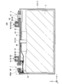
- FIG. 1 is a longitudinal sectional view of a power storage device of Example 1.
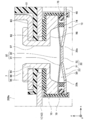
- FIG. FIG. 2 is an enlarged view of a broken line portion 200 a of FIG. 1, showing a conduction state of the current interrupting device of the first embodiment.
- the enlarged view which shows the modification of the current interrupting apparatus of Example 1.
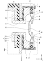
- FIG. The enlarged view (figure corresponding to the broken-line part 200a of FIG. 1) which shows the state (non-conduction state) after the action
- 7 is a longitudinal sectional view of a power storage device of Example 3.
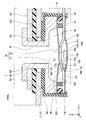
- FIG. 7 is an enlarged view of a broken line portion 400 a of FIG. 6, showing the conduction state of the current interrupting device of the third embodiment.
- the enlarged view of the electric current interruption apparatus with which the electrical storage apparatus of Example 4 is equipped (equivalent to the broken line part 400a of FIG. 6).
- the enlarged view of the electric current interruption apparatus with which the electrical storage apparatus of Example 5 is equipped (equivalent to the broken line part 400a of FIG. 6).
- the enlarged view of the electric current interruption apparatus with which the electrical storage apparatus of Example 6 is equipped (equivalent to the broken-line part 200a of FIG. 2).
- the first deformation plate includes an abutting portion that abuts against the central portion of the current-carrying plate in the conductive state, and a first facing portion that faces the inclined portion of the current-carrying plate.
- the lower surface of the first opposing portion of the first deformation plate is energized as it is separated from the contact portion. You may incline so that distance with the inclination part of a board may become long.
- the plate may be constant in the inclined portion. According to such a configuration, molding of the current-carrying plate can be facilitated, and cost and molding time can be reduced.
- the current interrupting device disclosed in the present specification is provided on the side opposite to the first deformation plate with respect to the current passing plate, and is provided with a protrusion protruding toward the central portion of the current passing plate.
- the second deformation plate may be further provided.
- the protrusion is at the first position in the conductive state, and the protrusion is in the first position from the first position in the non-conductive state. It may be switched to the second state in which it moves to the second position on the side to separate the current-carrying plate and the first deformation plate.
- the second deformation plate has a second central portion having a protrusion in a conductive state, and a second opposing portion facing the inclined portion of the conduction plate. May be Further, when the current-carrying plate and the second deformation plate are viewed in the first direction or the second direction in the conductive state, the upper surface of the second facing portion of the second deformation plate is shifted from the second central portion. You may incline so that distance with an inclination part may become short. The angle between the lower surface of the inclined portion and the lower surface of the central portion may be smaller than the angle between the upper surface of the central portion and the upper surface of the second opposing portion.
- the outer peripheral portion of the current carrying plate may further have a flat portion extending outward from the outer peripheral edge of the inclined portion. Further, the upper surface of the central portion of the current-carrying plate may be substantially parallel to the upper surface of the flat portion.
- the first facing portion of the first deformation plate may further face the flat portion of the current-carrying plate.
- the power storage device 100 includes a case 1, an electrode assembly 3 housed in the case 1, and terminals 5 and 7 as electrode terminals fixed to the case 1.
- the electrode assembly 3 and the terminals 5 and 7 are electrically connected.
- Power storage device 100 further includes a current interrupting device 10 disposed between electrode assembly 3 and terminal 7.
- the electrolytic solution is injected into the inside of the case 1, and the electrode assembly 3 is immersed in the electrolytic solution.
- the cross-sectional view shown in FIG. 1 shows a cross section passing through the centers of the current-carrying plate 20 and the first deformation plate 30 described later.
- the case 1 is made of metal and is a box-shaped member having a substantially rectangular parallelepiped shape.
- the case 1 includes a main body 111 and a lid 112 fixed to the main body 111.
- the lid 112 covers the top of the main body 111. Openings 81 and 82 are formed in the lid 112.
- the terminal 5 communicates with the inside and the outside of the case 1 through the opening 81, and the terminal 7 communicates with the inside and the outside of the case 1 through the opening 82.
- the electrode assembly 3 includes a positive electrode sheet, a negative electrode sheet, and a separator disposed between the positive electrode sheet and the negative electrode sheet.
- the electrode assembly 3 is configured by laminating a plurality of positive electrode sheets, a plurality of negative electrode sheets, and a plurality of separators.
- the positive electrode sheet and the negative electrode sheet include a current collecting member and an active material layer formed on the current collecting member.
- a current collection member what is used for a positive electrode sheet is aluminum foil, for example, and what is used for a negative electrode sheet is copper foil, for example.
- the electrode assembly 3 also includes a positive electrode current collecting tab 41 and a negative electrode current collecting tab 42.
- the positive electrode current collection tab 41 is formed on the upper end portion of the positive electrode sheet.
- the negative electrode current collection tab 42 is formed on the upper end portion of the negative electrode sheet.
- the positive electrode current collecting tab 41 and the negative electrode current collecting tab 42 protrude above the electrode assembly 3.
- the positive electrode current collection tab 41 is fixed to the positive electrode lead 43.
- the negative electrode current collection tab 42 is fixed to the negative electrode lead 44.
- the positive electrode lead 43 is connected to the positive electrode current collecting tab 41 and the terminal 5.
- the positive electrode current collection tab 41 and the terminal 5 are electrically connected via the positive electrode lead 43.
- An insulating member 72 is disposed between the positive electrode lead 43 and the case 1. The insulating member 72 insulates the positive electrode lead 43 and the lid portion 112 of the case 1.
- the negative electrode lead 44 is connected to the negative electrode current collection tab 42 and the connection terminal 46.
- the connection terminal 46 is electrically connected to the terminal 7 via the current interrupting device 10.
- the negative electrode current collection tab 42 and the terminal 7 are electrically connected via the negative electrode lead 44, the connection terminal 46 and the current interrupting device 10.
- a conduction path connecting the electrode assembly 3 and the terminal 7 is formed.
- the current interrupting device 10 can interrupt this current path.
- the configuration of the current interrupting device 10 will be described later.
- An insulating member 73 is disposed between the negative electrode lead 44 and the case 1. The insulating member 73 insulates the negative electrode lead 44 from the case 1.
- Gaskets 62 and 63 made of resin are disposed on the upper surface of the lid 112.
- the gasket 62 has a protrusion 66 projecting upward from the lid 112 and a flat plate 68 extending along the lid 112.
- the protrusion 66 is disposed on the center side of the opening 81 of the lid 112, and the flat plate 68 is disposed on the opening 81 of the lid 112.
- An external terminal 60 is disposed on the top surface of the gasket 62 along the shape of the top surface of the gasket 62.
- the head of the bolt 64 is disposed in a bottomed hole 62 a formed in the projection 66.
- the shaft portion of the bolt 64 protrudes upward through the opening of the external terminal 60.
- the terminal 5, the external terminal 60, and the bolt 64 are electrically connected to one another to constitute a positive electrode terminal.
- the configurations of the gasket 63, the external terminal 61 and the bolt 65 are the same as the configurations of the gasket 62, the external terminal 60 and the bolt 64 described above.
- the terminal 7, the external terminal 61, and the bolt 65 are electrically connected to one another to form a negative electrode terminal.
- the terminal 7 will be described with reference to FIG. As shown in FIG. 2, the terminal 7 is fixed to the case 1 by caulking.
- the terminal 7 includes a cylindrical portion 94, a base portion 95 and a fixing portion 96.
- the cylindrical portion 94 is inserted into the opening 82.
- a through hole 97 is formed in the cylindrical portion 94.
- the base portion 95 is annularly formed.
- the base portion 95 is fixed to the lower end portion of the cylindrical portion 94.
- the base 95 is disposed inside the case 1.
- the recess 95 is formed in the base portion 95.
- the recess 98 communicates with the through hole 97, and the inside of the recess 98 is maintained at atmospheric pressure.
- the fixing portion 96 is formed in an annular shape, and is disposed at the upper end portion of the cylindrical portion 94.
- the fixing portion 96 is disposed outside the case 1.
- the terminal 7 is fixed to the lid 112 of the case 1 by the fixing portion 96.
- the current interrupting device 10 includes a current-carrying plate 20 and a first deformation plate 30.
- the current-carrying plate 20 is a metal plate having a constant thickness and has conductivity.
- the conduction plate 20 is formed in a circular shape in plan view (as viewed from the z direction), and is disposed below the first deformation plate 30.
- the energizing plate 20 has an outer peripheral portion 21 and a central portion 22. In the outer peripheral portion 21, an inclined portion 23 is formed adjacent to the central portion 22. When viewed along a direction (x direction or y direction) parallel to the upper surface of the central portion 22 (for example, when viewed from the y direction as shown in FIG.
- the inclined portion 23 moves away from the central portion 22 It inclines so that the distance with the 1 deformation board 30 may become long. That is, the inclined portion 23 is inclined downward from the central portion 22 toward the outer peripheral direction.
- the central portion 22 is formed in a planar shape extending in the x direction and the y direction (horizontal direction).
- the outer peripheral portion 21 of the conducting plate 20 is bent at the outer peripheral end of the inclined portion 23 and extends in the horizontal direction (x direction or y direction), and the connection terminal 46 is connected to the outer peripheral edge thereof.
- Grooves 20 a are formed on the lower surface of the current-carrying plate 20.
- the groove portion 20 a is formed around the central portion 22, and the current-carrying plate 20 and the first deformation plate 30 are connected inside the groove portion 20 a.
- the mechanical strength of the plate 20 at the position where the groove 20a is formed is lower than the mechanical strength of the plate 20 at a position other than the groove 20a.
- a vent hole 20 b is formed in the conduction plate 20, and the space 50 between the first deformation plate 30 and the conduction plate 20 communicates with the space in the case 1.
- the first deformation plate 30 is a circular conductive diaphragm in plan view (as viewed in the z direction), and is downwardly convex.
- the thickness of the first deformation plate 30 is constant and thinner than the thickness of the current-carrying plate 20.
- the first deformation plate 30 has a first facing portion 31 and a contact portion 32.
- the contact portion 32 is connected to the central portion 22 of the current-carrying plate 20 by welding.
- the first facing portion 31 is formed at a position facing the inclined portion 23 of the current-carrying plate 20. That is, the length in the radial direction of the first opposing portion 31 of the first deformation plate 30 and the length in the radial direction of the inclined portion 23 of the current-carrying plate 20 are substantially the same when viewed in plan.
- the first facing portion 31 is inclined such that the distance to the current-carrying plate 20 becomes longer as it goes away from the contact portion 32 when viewed along the x direction or y direction. That is, the first opposing portion 31 is inclined upward from the contact portion 32 toward the outer peripheral direction.
- the outer peripheral side of the first facing portion 31 is connected to the outer peripheral portion of the lower surface of the base portion 95, and the lower end of the recess 98 of the base portion 95 is covered with the first deformation plate 30. Since the inside of the recess 98 is maintained at the atmospheric pressure, the atmospheric pressure acts on the upper surface of the first deformation plate 30.
- a seal member 75 is provided between the current-carrying plate 20 and the outer peripheral portion of the base portion 95.
- the seal member 75 is in contact with the lower surface of the base portion 95 and the upper surface of the current-carrying plate 20, and makes a round in the circumferential direction on the outer peripheral side of the base portion 95.
- the seal member 75 seals between the base portion 95 and the energizing plate 20.
- the seal member 75 is, for example, an O-ring made of ethylene-propylene rubber (EPM) such as ethylene-propylene-diene rubber (EPDM).
- EPM ethylene-propylene rubber
- EPDM ethylene-propylene-diene rubber
- the sealing member 75 is not limited to the above, and a material having sealing properties, insulating properties, electrolytic solution resistance, and elasticity may be used.
- an insulating member 74 is disposed between the conduction plate 20 and the first deformation plate 30.
- the insulating member 74 is an annular member, and is in contact with a portion outside the inclined portion 23 of the conduction plate 20 and a portion outside the first opposing portion 31 of the first deformation plate 30.
- the insulating member 74 is disposed inside the seal member 75. Note that, as shown in FIG. 3, the inclined portion 23 is on the outer peripheral side such that the position of the outer peripheral end of the inclined portion 23 of the conductive plate 20 in plan view is substantially the same as the position of the inner peripheral end of the insulating member 74. It may extend. In this case, the vent holes 20 b are formed in the inclined portion 23.
- the energizing plate 20, the first deformation plate 30, and the base portion 95 are fixed by a fixing member 70.
- the fixing member 70 crimps and fixes the current-carrying plate 20, the first deformation plate 30, and the base portion 95.
- An insulating member 79 is disposed inside the fixing member 70. The insulating member 79 insulates the current-carrying plate 20, the first deformation plate 30 and the terminal 7 (the base portion 95) from the fixing member 70.
- the current interrupting device 10 has a conduction path connecting the connection terminal 46, the conduction plate 20, the first deformation plate 30, and the terminal 7 in series. For this reason, the electrode assembly 3 and the terminal 7 are electrically connected via the conduction path of the current interrupting device 10.
- the terminal 5 and the terminal 7 are used in a conductive state in which current can be supplied via an external device (for example, a generator, a motor, etc.).
- an external device for example, a generator, a motor, etc.
- the pressure acting on the lower surface of the first deformation plate 30 via the vent holes 20b increases.
- atmospheric pressure acts on the upper surface of the first deformation plate 30. For this reason, when the internal pressure of the case 1 rises and reaches a predetermined value, the first deformation plate 30 is inverted to be in a state of being convex upward.
- the current-carrying plate 20 connected to the contact portion 32 of the first deformation plate 30 is broken starting from the mechanically fragile groove portion 20a.
- the conduction path connecting the conduction plate 20 and the first deformation plate 30 is cut off, and the electrode assembly 3 and the terminal 7 are brought out of conduction.
- the first deformation plate 30 is insulated from the connection terminal 46, and the conduction plate 20 is insulated from the terminal 7.
- the first deformation plate 30 buckles near the middle point between the connection portion with the base portion 95 and the contact portion 32. There is. That is, the plate thickness of the first deformation plate 30 is thin, and its mechanical strength is low. For this reason, when the current-carrying plate 20 is broken and a large force acts instantaneously on the first deformation plate 30, the first deformation plate 30 may buckle in the vicinity of the intermediate point. At this time, as shown in FIG. 4, the buckling portion 34 of the first deformation plate 30 protrudes below the other portion of the first deformation plate 30.
- each of the inclined portion 23 of the conducting plate 20 and the first opposing portion 31 of the first deformation plate 30 is inclined downward and upward, the distance between them is the outer peripheral end of the energizing plate 20. It is formed to become longer as it goes to. Therefore, after the operation of the current interrupting device 10, a sufficient distance between the buckling portion 34 and the conduction plate 20 can be secured, and the buckling portion 34 of the first deformation plate 30 and the conduction plate 20 contact with each other. Can be suppressed. As a result, re-conduction between the first deformation plate 30 and the conduction plate 20 can be suppressed.
- the conducting plate 20 is formed using a plate material having a constant thickness. For this reason, compared with the prior art, shaping
- a power storage device according to a second embodiment will be described with reference to FIG.
- the configuration of the current interrupting device is different from that of the first embodiment, and the other configuration is the same as that of the first embodiment.
- the current interrupting device 10 a includes a conduction plate 20, a first deformation plate 30, and a second deformation plate 40 made of metal.
- the second deformation plate 40 is a circular diaphragm.
- the center position of the second deformation plate 40 substantially coincides with the center position of the first deformation plate 30 and the center position of the current-carrying plate 20 in plan view (as viewed in the z direction).
- the second deformation plate 40 has a second facing portion 47 and a central portion 48.
- the second deformation plate 40 is disposed below the conduction plate 20, and a central portion 48 thereof protrudes downward.
- the second facing portion 47 is formed at a position facing the inclined portion 23 of the conduction plate 20. That is, the length in the radial direction of the second facing portion 47 of the second deformation plate 40 and the length in the radial direction of the inclined portion 23 of the conduction plate 20 are substantially the same when viewed in plan.
- the second facing portion 47 is inclined such that the distance to the current-carrying plate 20 becomes shorter as it goes away from the central portion 48 when viewed along the x direction or y direction. That is, the second opposing portion 47 is inclined upward from the central portion 48 toward the outer peripheral direction.
- Central unit 48 which is formed in a planar shape extending in the x-direction and y-direction (horizontal direction), the angle between the upper surface of the upper surface and the second opposing portion 47 of the central portion 48 has a theta 1.
- the angle theta 2 between the lower surface and the lower surface of the central portion 22 of the inclined portion 23 is smaller than the angle theta 1 between the upper surface and the upper surface of the second opposing portion 47 of the central portion 48.
- the upper surface of the outer peripheral side of the second opposing portion 47 of the second deformation plate 40 is fixed to the lower surface of the outer peripheral portion of the current-carrying plate 20 by welding. Further, on the upper surface of the central portion 48 of the second deformation plate 40, a protruding portion 40a which protrudes upward is provided. The central portion 22 of the conducting plate 20 is located above the projecting portion 40 a. The pressure of the space 130 in the case 1 acts on the lower surface of the second deformation plate 40 (described later). Space 130 is sealed from the space in case 1.
- the conduction plate 20 is disposed between the second deformation plate 40 and the first deformation plate 30, and the conduction plate 20 is formed with a vent hole 20 b.
- the space 130 is in communication with the space 132 between the first deformation plate 30 and the conduction plate 20 via the vent hole 20 b.
- the first deformation plate 30 is disposed above the conduction plate 20.
- a space 134 is formed on the top surface of the first deformation plate 30. Space 134 is maintained at atmospheric pressure.
- the second deformation plate 40, the current-carrying plate 20, the first deformation plate 30, and the base portion 95 are fixed by a fixing member 80.
- the fixing member 80 caulks and fixes the second deformation plate 40, the current-carrying plate 20, the first deformation plate 30, and the base portion 95.
- An insulating member 89 is disposed inside the fixing member 80. The insulating member 89 insulates the second deformation plate 40, the conduction plate 20, the first deformation plate 30, and the terminal 7 (the base portion 95) from the fixing member 80.
- the current interrupting device 10a has a conduction path connecting the connection terminal 46, the conduction plate 20, the first deformation plate 30, and the terminal 7 in series. Therefore, the electrode assembly 3 and the terminal 7 are electrically connected via the current path of the current interrupting device 10a.
- movement of the electric current interruption apparatus 10a is demonstrated.
- the pressure acting on the lower surface of the second deformation plate 40 rises.
- the pressure of the space 130 sealed from the space in the case 1 acts on the upper surface of the second deformation plate 40.
- the second deformation plate 40 is reversed, and the state of being convex downward changes to the state of convex upward.
- the air in the space 130 moves to the space 132 through the vent holes 20 b, and the pressure in the space 132 rises.
- the projecting portion 40a of the second deformation plate 40 collides with the central portion 22 of the conduction plate 20, and the conduction plate 20 is broken at the groove portion 20a.
- the first deformation plate 30 is reversed, and the first deformation plate 30 and the central portion 22 of the conduction plate 20 are displaced upward.
- the conduction path connecting the conduction plate 20 and the first deformation plate 30 is cut off, and the conduction between the electrode assembly 3 and the terminal 7 is cut off.
- the first deformation plate 30 is insulated from the connection terminal 46 and the conduction plate 20 is insulated from the terminal 7.
- the conductive plate 20 and the first deformation plate 30 are inclined in the same manner as those of the first embodiment, the same function and effect as the power storage device 100 of the first embodiment can be obtained. .
- the current interrupting device 10a of the present embodiment the angle theta 2 between the lower surface and the lower surface of the central portion 22 of the inclined portion 23, an angle theta 1 between the upper surface and the upper surface of the second opposing portion 47 of the central portion 48 It is smaller than that. That is, in the space surrounded by the current-carrying plate 20 and the second deformation plate 40, the space formed above the position where the current-carrying plate 20 and the second deformation plate 40 abut is the current-carrying plate 20 and the second deformation plate The space 40 is larger than the space formed below the contact position with the space 40. Thus, it is possible to secure a space in which the second deformation plate 40 reverses at the time of operation of the current interrupting device 10a, and the second deformation plate 40 can be suitably reversed.
- the power storage device of the third embodiment differs in the configuration of each member (162, 163, 164, 165, etc.) disposed on the upper surface of the lid 112 in the first embodiment and the configuration of the current-carrying plate 120.
- the other configuration is the same as that of the first embodiment, and thus the detailed description thereof is omitted.
- gaskets 162 and 163 made of resin are disposed on the top surface of the lid 112.
- An external terminal 60 is disposed on the top surface of the gasket 162.
- a through hole 60 a is formed in the external terminal 60.
- the size of the lower surface side of the through hole 60 a is larger than that of the upper surface side of the external terminal 60.
- the gasket 162 insulates the lid 112 and the external terminal 60.
- the bolt 164 passes through the through hole 60a. Specifically, the head of the bolt 164 is accommodated in the through hole 60a. Further, the shaft portion of the bolt 164 protrudes above the external terminal 60 through the through hole 60 a.
- the terminal 5, the external terminal 60, and the bolt 164 are electrically connected to one another to constitute a positive electrode terminal.
- the configurations of the gasket 163, the external terminal 61 and the bolt 165 are similar to the configurations of the gasket 162, the external terminal 60 and the bolt 164 described above.
- the terminal 7, the external terminal 61, and the bolt 165 are electrically connected to one another to form a negative electrode terminal.
- the current-carrying plate 120 has an outer peripheral portion 121 and a central portion 122.
- An inclined portion 123 and a flat portion 124 are formed in the outer peripheral portion 121 of the current-carrying plate 120.
- the inclined portion 123 is formed adjacent to the outer peripheral end of the central portion 122.
- the flat portion 124 is formed adjacent to the outer peripheral end of the inclined portion 123.
- the flat portion 124 is bent at the outer peripheral end of the inclined portion 123 and extends in the horizontal direction, and the connection terminal 46 is connected to the outer peripheral edge thereof.
- the position of the boundary between the inclined portion 123 and the flat portion 124 in a plan view is located radially inward of the position of the inner peripheral end of the insulating member 74.
- the inclined portion 123 is formed at an acute angle with respect to the xy plane as compared with the first embodiment. Therefore, when the first deformation plate 30 is buckled (see FIG. 4), the distance between the first deformation plate 30 and the current-carrying plate 120 can be further secured. That is, re-conduction between the first deformation plate 30 and the conduction plate 120 can be further suppressed.
- the configurations of the gaskets 162 and 163, the bolts 164 and 165, and the like may be used in the other embodiments described above.
- the second deformation plate 40 described in the second embodiment is provided.
- the second facing portion 47 of the second deformation plate 40 is formed at a position facing the inclined portion 123 and the flat portion 124 of the energizing plate 120. That is, the length obtained by adding the radial length of the second facing portion 47 of the second deformation plate 40 and the radial length of the inclined portion 123 and the flat portion 124 of the current-carrying plate 120 when viewed in plan is It becomes almost the same.
- the angle theta 3 between the lower surface and the lower surface of the central portion 122 of the inclined portion 123 is smaller than the angle theta 1 between the upper surface and the upper surface of the second opposing portion 47 of the central portion 48.
- the conductive plate 120 and the first deformation plate 30 are inclined in the same manner as those of the first embodiment, the same function and effect as the power storage device 100 of the first embodiment can be obtained. .
- the configuration of the second deformation plate is different from the fourth embodiment, and the other configuration is the same as that of the fourth embodiment.
- the second deformation plate 140 has a second facing portion 147 and a central portion 148.
- the second facing portion 147 of the second deformation plate 140 is formed at a position facing the inclined portion 123 of the energizing plate 120.
- the second deformation plate 140 is connected to the conduction plate 120 on the outer peripheral side of the second facing portion 147.
- the length in the radial direction of the second facing portion 147 of the second deformation plate 140 and the length in the radial direction of the sloping portion 123 of the conduction plate 120 are substantially the same when viewed in plan view.
- the position of the outer peripheral end of the second opposing portion 147 of the plate 140 is located radially inward of the position of the inner peripheral end of the insulating member 74.
- the angle theta 3 between the lower surface and the lower surface of the central portion 122 of the inclined portion 123 is smaller than the angle theta 4 between the upper surface and the upper surface of the second opposing portion 147 of the central portion 148.
- the positions of the groove portions of the first embodiment and the conduction plate 20 are different.
- the groove portion 20a is provided at the boundary between the central portion 21 of the conduction plate 20 and the inclined portion 23.
- the groove portion 20c of the conduction plate 20 of the sixth embodiment is provided in the central portion 21 of the conduction plate 20. It is done. That is, in plan view, the groove 20 c is formed inside the boundary between the central portion 21 and the inclined portion 23 in the radial direction of the current-carrying plate 20.
- the current-carrying plate may be formed into the shape shown in the drawings after the groove is formed in the plate-like member.
- the breaking load (the load at which the current-carrying plate 20 breaks due to the pressure in the case) is determined by the shape and depth of the groove. Therefore, in the power storage device of the sixth embodiment, stress applied to the groove 20c and the groove 20c at the time of molding of the current-carrying plate 20 are compared with the case where the groove 20c is formed at the boundary between the central portion 21 and the inclined portion 23. Deformation is suppressed, so the breaking load can be stabilized. That is, manufacturing variations of the power storage device can be reduced.
- communication holes may be formed in the first deformation plate 30 to connect the space 132 and the space 134, and the spaces 130 and 132 may be maintained at atmospheric pressure.
- the current interrupting device 10 may be provided on the terminal 5 side, or may be provided on both the terminal 5 and the terminal 7.
- an insulating member can be disposed between the terminal 5 and the lid 112 in the same manner as the configuration of the above embodiment.
- the first deformation plate 30 is reversed to cut off the conduction with the conduction plate 20.
- the mode of deformation of the first deformation plate 30 is not limited to inversion.
- the contact portion 32 of the first deformation plate 30 is bent upward, the conduction plate 20 is broken starting from the groove 20a, and the conduction between the first deformation plate 30 and the conduction plate 20 is interrupted. May be The first deformation plate 30 may be deformed in any way as long as the conduction between the first deformation plate 30 and the conduction plate 20 is interrupted. The same applies to the second deformation plate 40.
Landscapes
- Engineering & Computer Science (AREA)
- Power Engineering (AREA)
- Microelectronics & Electronic Packaging (AREA)
- Chemical & Material Sciences (AREA)
- Chemical Kinetics & Catalysis (AREA)
- Electrochemistry (AREA)
- General Chemical & Material Sciences (AREA)
- Connection Of Batteries Or Terminals (AREA)
Abstract
Description
Claims (6)
- ケース内に収容され、
前記ケースに収容される電極組立体と前記ケースに設けられる電極端子とを電気的に接続された導通状態と、電気的に非接続となる非導通状態とに切換える電流遮断装置であって、
前記電極組立体に電気的に接続される通電板と、
前記通電板と対向して配置され、前記電極端子に電気的に接続される第1変形板と、を備えており、
前記通電板は、中央部と、該中央部を取り囲む外周部を有しており、
前記第1変形板は、前記導通状態においては前記通電板と前記中央部において当接して電気的に接続している一方で、前記非導通状態においては前記通電板から離間して前記通電板と電気的に非接続となり、
前記通電板の中央部の上面は、前記導通状態において、第1方向及び該第1方向に直交する第2方向に広がる平面状に形成されており、
前記通電板の外周部は、前記中央部の境界から外側に広がる傾斜部を有しており、
前記導通状態において前記通電板及び前記第1変形板を前記第1方向又は前記第2方向に沿って見ると、前記傾斜部の上面は、前記中央部から離れるにしたがって前記第1変形板との距離が長くなるように傾斜している、電流遮断装置。 - 前記第1変形板は、前記導通状態において前記通電板の中央部と当接する当接部と、前記通電板の傾斜部と対向する第1対向部を有しており、
前記導通状態において前記通電板及び前記第1変形板を前記第1方向又は前記第2方向に沿って見ると、前記第1変形板の第1対向部の下面は、前記当接部から離れるにしたがって前記通電板の傾斜部との距離が長くなるように傾斜している、請求項1に記載の電流遮断装置。 - 前記通電板は、前記傾斜部において板厚が一定である、請求項1または2に記載の電流遮断装置。
- 前記通電板に対して前記第1変形板とは反対側に配置されているとともに、前記通電板の中央部に向かって突出している突起が設けられている第2変形板をさらに備えており、
前記第2変形板は、前記導通状態においては前記突起が第1位置に位置して前記通電板と前記第1変形板とが当接している第1状態と、前記非導通状態においては前記突起が前記第1位置から前記通電板側の第2位置に移動して前記通電板と前記第1変形板とを離間させる第2状態とに切り替えられる、請求項1~3のいずれか一項に記載の電流遮断装置。 - 前記第2変形板は、前記導通状態において、前記突起を有する中心部と、前記通電板の傾斜部と対向する第2対向部とを有しており、
前記導通状態において前記通電板及び前記第2変形板を前記第1方向又は前記第2方向に沿って見ると、前記第2変形板の前記第2対向部の上面は、前記中心部から離れるにしたがって前記通電板の傾斜部との距離が短くなるように傾斜しており、
前記傾斜部の下面と前記中央部の下面とのなす角度は、前記中心部の上面と前記第2対向部の上面とのなす角度よりも小さい、請求項4に記載の電流遮断装置。 - 請求項1から5のいずれか一項に記載の電流遮断装置を備える蓄電装置。
Priority Applications (3)
| Application Number | Priority Date | Filing Date | Title |
|---|---|---|---|
| US15/577,540 US10361422B2 (en) | 2015-05-29 | 2016-05-11 | Current interruption device and electricity storage device including the same |
| DE112016002419.3T DE112016002419T5 (de) | 2015-05-29 | 2016-05-11 | Stromunterbrechungsvorrichtung und Elektrizitätsspeichervorrichtung, die diese umfasst |
| JP2017521766A JP6573975B2 (ja) | 2015-05-29 | 2016-05-11 | 電流遮断装置及びこれを備える蓄電装置 |
Applications Claiming Priority (2)
| Application Number | Priority Date | Filing Date | Title |
|---|---|---|---|
| JP2015110316 | 2015-05-29 | ||
| JP2015-110316 | 2015-05-29 |
Publications (1)
| Publication Number | Publication Date |
|---|---|
| WO2016194571A1 true WO2016194571A1 (ja) | 2016-12-08 |
Family
ID=57440694
Family Applications (1)
| Application Number | Title | Priority Date | Filing Date |
|---|---|---|---|
| PCT/JP2016/064058 Ceased WO2016194571A1 (ja) | 2015-05-29 | 2016-05-11 | 電流遮断装置及びこれを備える蓄電装置 |
Country Status (4)
| Country | Link |
|---|---|
| US (1) | US10361422B2 (ja) |
| JP (1) | JP6573975B2 (ja) |
| DE (1) | DE112016002419T5 (ja) |
| WO (1) | WO2016194571A1 (ja) |
Cited By (1)
| Publication number | Priority date | Publication date | Assignee | Title |
|---|---|---|---|---|
| CN110165136A (zh) * | 2018-02-12 | 2019-08-23 | 株式会社Lg化学 | 电流中断装置和包括该电流中断装置的电池模块 |
Families Citing this family (2)
| Publication number | Priority date | Publication date | Assignee | Title |
|---|---|---|---|---|
| CN111029489B (zh) | 2019-08-14 | 2021-08-17 | 宁德时代新能源科技股份有限公司 | 二次电池 |
| CN111029488B (zh) * | 2019-08-14 | 2021-07-30 | 宁德时代新能源科技股份有限公司 | 二次电池 |
Citations (4)
| Publication number | Priority date | Publication date | Assignee | Title |
|---|---|---|---|---|
| JPH11176417A (ja) * | 1997-12-16 | 1999-07-02 | Fuji Elelctrochem Co Ltd | 密閉型2次電池 |
| JP2005108503A (ja) * | 2003-09-29 | 2005-04-21 | Shin Kobe Electric Mach Co Ltd | リチウム二次電池 |
| JP2014002901A (ja) * | 2012-06-18 | 2014-01-09 | Toyota Industries Corp | 電流遮断装置およびこれを備えた蓄電装置 |
| JP2014086319A (ja) * | 2012-10-24 | 2014-05-12 | Toyota Motor Corp | 二次電池 |
Family Cites Families (2)
| Publication number | Priority date | Publication date | Assignee | Title |
|---|---|---|---|---|
| JP5081932B2 (ja) | 2010-01-25 | 2012-11-28 | 日立ビークルエナジー株式会社 | 密閉型電池およびその製造方法 |
| JP5806262B2 (ja) * | 2013-07-30 | 2015-11-10 | 株式会社豊田自動織機 | 電流遮断装置及びそれを用いた蓄電装置 |
-
2016
- 2016-05-11 WO PCT/JP2016/064058 patent/WO2016194571A1/ja not_active Ceased
- 2016-05-11 DE DE112016002419.3T patent/DE112016002419T5/de not_active Withdrawn
- 2016-05-11 JP JP2017521766A patent/JP6573975B2/ja active Active
- 2016-05-11 US US15/577,540 patent/US10361422B2/en active Active
Patent Citations (4)
| Publication number | Priority date | Publication date | Assignee | Title |
|---|---|---|---|---|
| JPH11176417A (ja) * | 1997-12-16 | 1999-07-02 | Fuji Elelctrochem Co Ltd | 密閉型2次電池 |
| JP2005108503A (ja) * | 2003-09-29 | 2005-04-21 | Shin Kobe Electric Mach Co Ltd | リチウム二次電池 |
| JP2014002901A (ja) * | 2012-06-18 | 2014-01-09 | Toyota Industries Corp | 電流遮断装置およびこれを備えた蓄電装置 |
| JP2014086319A (ja) * | 2012-10-24 | 2014-05-12 | Toyota Motor Corp | 二次電池 |
Cited By (3)
| Publication number | Priority date | Publication date | Assignee | Title |
|---|---|---|---|---|
| CN110165136A (zh) * | 2018-02-12 | 2019-08-23 | 株式会社Lg化学 | 电流中断装置和包括该电流中断装置的电池模块 |
| US11189892B2 (en) | 2018-02-12 | 2021-11-30 | Lg Chem, Ltd. | Current interrupt device having connection parts with contacting inclined surfaces and battery module including the same |
| US11881599B2 (en) | 2018-02-12 | 2024-01-23 | Lg Energy Solution, Ltd. | Current interrupt device having connection parts with contacting inclined surfaces and battery module including the same |
Also Published As
| Publication number | Publication date |
|---|---|
| US10361422B2 (en) | 2019-07-23 |
| JP6573975B2 (ja) | 2019-09-11 |
| JPWO2016194571A1 (ja) | 2018-03-01 |
| US20180183035A1 (en) | 2018-06-28 |
| DE112016002419T5 (de) | 2018-04-12 |
Similar Documents
| Publication | Publication Date | Title |
|---|---|---|
| US8951663B2 (en) | Secondary battery | |
| US8709632B2 (en) | Battery module | |
| JP5609935B2 (ja) | 蓄電装置および車両 | |
| JP6296153B2 (ja) | 蓄電装置 | |
| JP2015028882A (ja) | 電流遮断装置及びそれを用いた蓄電装置 | |
| KR20150016360A (ko) | 이차 전지 집전 단자 및 이차 전지 | |
| CN107039628A (zh) | 二次电池和电池组 | |
| JP6573975B2 (ja) | 電流遮断装置及びこれを備える蓄電装置 | |
| JP6176338B2 (ja) | 蓄電装置 | |
| JP2015167085A (ja) | 蓄電装置 | |
| JP6453726B2 (ja) | 電流遮断装置、蓄電装置、電流遮断装置の製造方法、および蓄電装置の製造方法 | |
| JP6456802B2 (ja) | 電流遮断装置とそれを用いた蓄電装置 | |
| JP6533299B2 (ja) | 電流遮断装置及びこれを用いた蓄電装置 | |
| JP6281423B2 (ja) | 蓄電装置 | |
| JP6597201B2 (ja) | 蓄電装置 | |
| JP6357132B2 (ja) | 電流遮断装置及びそれを用いた蓄電装置 | |
| JP6433866B2 (ja) | 電流遮断装置及びこれを用いた蓄電装置 | |
| JP6520304B2 (ja) | 蓄電装置 | |
| JP6716343B2 (ja) | 電流遮断装置、蓄電装置及び蓄電装置の製造方法 | |
| JP6453725B2 (ja) | 電流遮断装置およびこれを備える蓄電装置 | |
| JP6393245B2 (ja) | 電流遮断装置とそれを用いた蓄電装置 | |
| JP2017022113A (ja) | 蓄電装置 | |
| JP6610091B2 (ja) | 蓄電装置 | |
| JP6265019B2 (ja) | 蓄電装置 | |
| JP6436875B2 (ja) | 電流遮断装置及びこれを用いた蓄電装置 |
Legal Events
| Date | Code | Title | Description |
|---|---|---|---|
| 121 | Ep: the epo has been informed by wipo that ep was designated in this application |
Ref document number: 16803008 Country of ref document: EP Kind code of ref document: A1 |
|
| ENP | Entry into the national phase |
Ref document number: 2017521766 Country of ref document: JP Kind code of ref document: A |
|
| WWE | Wipo information: entry into national phase |
Ref document number: 15577540 Country of ref document: US |
|
| WWE | Wipo information: entry into national phase |
Ref document number: 112016002419 Country of ref document: DE |
|
| 122 | Ep: pct application non-entry in european phase |
Ref document number: 16803008 Country of ref document: EP Kind code of ref document: A1 |