WO2016181859A1 - はんだ電極の製造方法およびその用途 - Google Patents
はんだ電極の製造方法およびその用途 Download PDFInfo
- Publication number
- WO2016181859A1 WO2016181859A1 PCT/JP2016/063365 JP2016063365W WO2016181859A1 WO 2016181859 A1 WO2016181859 A1 WO 2016181859A1 JP 2016063365 W JP2016063365 W JP 2016063365W WO 2016181859 A1 WO2016181859 A1 WO 2016181859A1
- Authority
- WO
- WIPO (PCT)
- Prior art keywords
- solder
- electrode
- substrate
- resist
- resin composition
- Prior art date
- Legal status (The legal status is an assumption and is not a legal conclusion. Google has not performed a legal analysis and makes no representation as to the accuracy of the status listed.)
- Ceased
Links
Images

Classifications
-
- G—PHYSICS
- G03—PHOTOGRAPHY; CINEMATOGRAPHY; ANALOGOUS TECHNIQUES USING WAVES OTHER THAN OPTICAL WAVES; ELECTROGRAPHY; HOLOGRAPHY
- G03F—PHOTOMECHANICAL PRODUCTION OF TEXTURED OR PATTERNED SURFACES, e.g. FOR PRINTING, FOR PROCESSING OF SEMICONDUCTOR DEVICES; MATERIALS THEREFOR; ORIGINALS THEREFOR; APPARATUS SPECIALLY ADAPTED THEREFOR
- G03F7/00—Photomechanical, e.g. photolithographic, production of textured or patterned surfaces, e.g. printing surfaces; Materials therefor, e.g. comprising photoresists; Apparatus specially adapted therefor
- G03F7/004—Photosensitive materials
- G03F7/022—Quinonediazides
- G03F7/023—Macromolecular quinonediazides; Macromolecular additives, e.g. binders
-
- B—PERFORMING OPERATIONS; TRANSPORTING
- B23—MACHINE TOOLS; METAL-WORKING NOT OTHERWISE PROVIDED FOR
- B23K—SOLDERING OR UNSOLDERING; WELDING; CLADDING OR PLATING BY SOLDERING OR WELDING; CUTTING BY APPLYING HEAT LOCALLY, e.g. FLAME CUTTING; WORKING BY LASER BEAM
- B23K1/00—Soldering, e.g. brazing, or unsoldering
- B23K1/20—Preliminary treatment of work or areas to be soldered, e.g. in respect of a galvanic coating
-
- G—PHYSICS
- G03—PHOTOGRAPHY; CINEMATOGRAPHY; ANALOGOUS TECHNIQUES USING WAVES OTHER THAN OPTICAL WAVES; ELECTROGRAPHY; HOLOGRAPHY
- G03F—PHOTOMECHANICAL PRODUCTION OF TEXTURED OR PATTERNED SURFACES, e.g. FOR PRINTING, FOR PROCESSING OF SEMICONDUCTOR DEVICES; MATERIALS THEREFOR; ORIGINALS THEREFOR; APPARATUS SPECIALLY ADAPTED THEREFOR
- G03F7/00—Photomechanical, e.g. photolithographic, production of textured or patterned surfaces, e.g. printing surfaces; Materials therefor, e.g. comprising photoresists; Apparatus specially adapted therefor
- G03F7/004—Photosensitive materials
- G03F7/022—Quinonediazides
- G03F7/023—Macromolecular quinonediazides; Macromolecular additives, e.g. binders
- G03F7/0233—Macromolecular quinonediazides; Macromolecular additives, e.g. binders characterised by the polymeric binders or the macromolecular additives other than the macromolecular quinonediazides
-
- G—PHYSICS
- G03—PHOTOGRAPHY; CINEMATOGRAPHY; ANALOGOUS TECHNIQUES USING WAVES OTHER THAN OPTICAL WAVES; ELECTROGRAPHY; HOLOGRAPHY
- G03F—PHOTOMECHANICAL PRODUCTION OF TEXTURED OR PATTERNED SURFACES, e.g. FOR PRINTING, FOR PROCESSING OF SEMICONDUCTOR DEVICES; MATERIALS THEREFOR; ORIGINALS THEREFOR; APPARATUS SPECIALLY ADAPTED THEREFOR
- G03F7/00—Photomechanical, e.g. photolithographic, production of textured or patterned surfaces, e.g. printing surfaces; Materials therefor, e.g. comprising photoresists; Apparatus specially adapted therefor
- G03F7/26—Processing photosensitive materials; Apparatus therefor
- G03F7/40—Treatment after imagewise removal, e.g. baking
-
- H—ELECTRICITY
- H05—ELECTRIC TECHNIQUES NOT OTHERWISE PROVIDED FOR
- H05K—PRINTED CIRCUITS; CASINGS OR CONSTRUCTIONAL DETAILS OF ELECTRIC APPARATUS; MANUFACTURE OF ASSEMBLAGES OF ELECTRICAL COMPONENTS
- H05K3/00—Apparatus or processes for manufacturing printed circuits
- H05K3/30—Assembling printed circuits with electric components, e.g. with resistors
- H05K3/32—Assembling printed circuits with electric components, e.g. with resistors electrically connecting electric components or wires to printed circuits
- H05K3/34—Assembling printed circuits with electric components, e.g. with resistors electrically connecting electric components or wires to printed circuits by soldering
- H05K3/3465—Application of solder
- H05K3/3468—Application of molten solder, e.g. dip soldering
-
- H—ELECTRICITY
- H05—ELECTRIC TECHNIQUES NOT OTHERWISE PROVIDED FOR
- H05K—PRINTED CIRCUITS; CASINGS OR CONSTRUCTIONAL DETAILS OF ELECTRIC APPARATUS; MANUFACTURE OF ASSEMBLAGES OF ELECTRICAL COMPONENTS
- H05K3/00—Apparatus or processes for manufacturing printed circuits
- H05K3/36—Assembling printed circuits with other printed circuits
- H05K3/368—Assembling printed circuits with other printed circuits parallel to each other
-
- H—ELECTRICITY
- H05—ELECTRIC TECHNIQUES NOT OTHERWISE PROVIDED FOR
- H05K—PRINTED CIRCUITS; CASINGS OR CONSTRUCTIONAL DETAILS OF ELECTRIC APPARATUS; MANUFACTURE OF ASSEMBLAGES OF ELECTRICAL COMPONENTS
- H05K3/00—Apparatus or processes for manufacturing printed circuits
- H05K3/40—Forming printed elements for providing electric connections to or between printed circuits
- H05K3/4007—Surface contacts, e.g. bumps
-
- H—ELECTRICITY
- H05—ELECTRIC TECHNIQUES NOT OTHERWISE PROVIDED FOR
- H05K—PRINTED CIRCUITS; CASINGS OR CONSTRUCTIONAL DETAILS OF ELECTRIC APPARATUS; MANUFACTURE OF ASSEMBLAGES OF ELECTRICAL COMPONENTS
- H05K3/00—Apparatus or processes for manufacturing printed circuits
- H05K3/40—Forming printed elements for providing electric connections to or between printed circuits
- H05K3/4038—Through-connections; Vertical interconnect access [VIA] connections
-
- H—ELECTRICITY
- H10—SEMICONDUCTOR DEVICES; ELECTRIC SOLID-STATE DEVICES NOT OTHERWISE PROVIDED FOR
- H10W—GENERIC PACKAGES, INTERCONNECTIONS, CONNECTORS OR OTHER CONSTRUCTIONAL DETAILS OF DEVICES COVERED BY CLASS H10
- H10W70/00—Package substrates; Interposers; Redistribution layers [RDL]
- H10W70/01—Manufacture or treatment
- H10W70/05—Manufacture or treatment of insulating or insulated package substrates, or of interposers, or of redistribution layers
- H10W70/093—Connecting or disconnecting other interconnections thereto or therefrom, e.g. connecting bond wires or bumps
-
- H—ELECTRICITY
- H10—SEMICONDUCTOR DEVICES; ELECTRIC SOLID-STATE DEVICES NOT OTHERWISE PROVIDED FOR
- H10W—GENERIC PACKAGES, INTERCONNECTIONS, CONNECTORS OR OTHER CONSTRUCTIONAL DETAILS OF DEVICES COVERED BY CLASS H10
- H10W72/00—Interconnections or connectors in packages
- H10W72/071—Connecting or disconnecting
- H10W72/072—Connecting or disconnecting of bump connectors
- H10W72/07231—Techniques
- H10W72/07236—Soldering or alloying
-
- H—ELECTRICITY
- H10—SEMICONDUCTOR DEVICES; ELECTRIC SOLID-STATE DEVICES NOT OTHERWISE PROVIDED FOR
- H10W—GENERIC PACKAGES, INTERCONNECTIONS, CONNECTORS OR OTHER CONSTRUCTIONAL DETAILS OF DEVICES COVERED BY CLASS H10
- H10W90/00—Package configurations
- H10W90/701—Package configurations characterised by the relative positions of pads or connectors relative to package parts
-
- H—ELECTRICITY
- H05—ELECTRIC TECHNIQUES NOT OTHERWISE PROVIDED FOR
- H05K—PRINTED CIRCUITS; CASINGS OR CONSTRUCTIONAL DETAILS OF ELECTRIC APPARATUS; MANUFACTURE OF ASSEMBLAGES OF ELECTRICAL COMPONENTS
- H05K2203/00—Indexing scheme relating to apparatus or processes for manufacturing printed circuits covered by H05K3/00
- H05K2203/05—Patterning and lithography; Masks; Details of resist
- H05K2203/0562—Details of resist
- H05K2203/0568—Resist used for applying paste, ink or powder
-
- H—ELECTRICITY
- H05—ELECTRIC TECHNIQUES NOT OTHERWISE PROVIDED FOR
- H05K—PRINTED CIRCUITS; CASINGS OR CONSTRUCTIONAL DETAILS OF ELECTRIC APPARATUS; MANUFACTURE OF ASSEMBLAGES OF ELECTRICAL COMPONENTS
- H05K3/00—Apparatus or processes for manufacturing printed circuits
- H05K3/30—Assembling printed circuits with electric components, e.g. with resistors
- H05K3/32—Assembling printed circuits with electric components, e.g. with resistors electrically connecting electric components or wires to printed circuits
- H05K3/34—Assembling printed circuits with electric components, e.g. with resistors electrically connecting electric components or wires to printed circuits by soldering
-
- H—ELECTRICITY
- H10—SEMICONDUCTOR DEVICES; ELECTRIC SOLID-STATE DEVICES NOT OTHERWISE PROVIDED FOR
- H10W—GENERIC PACKAGES, INTERCONNECTIONS, CONNECTORS OR OTHER CONSTRUCTIONAL DETAILS OF DEVICES COVERED BY CLASS H10
- H10W72/00—Interconnections or connectors in packages
- H10W72/01—Manufacture or treatment
- H10W72/012—Manufacture or treatment of bump connectors, dummy bumps or thermal bumps
-
- H—ELECTRICITY
- H10—SEMICONDUCTOR DEVICES; ELECTRIC SOLID-STATE DEVICES NOT OTHERWISE PROVIDED FOR
- H10W—GENERIC PACKAGES, INTERCONNECTIONS, CONNECTORS OR OTHER CONSTRUCTIONAL DETAILS OF DEVICES COVERED BY CLASS H10
- H10W72/00—Interconnections or connectors in packages
- H10W72/01—Manufacture or treatment
- H10W72/012—Manufacture or treatment of bump connectors, dummy bumps or thermal bumps
- H10W72/01231—Manufacture or treatment of bump connectors, dummy bumps or thermal bumps using blanket deposition
- H10W72/01233—Manufacture or treatment of bump connectors, dummy bumps or thermal bumps using blanket deposition in liquid form, e.g. spin coating, spray coating or immersion coating
-
- H—ELECTRICITY
- H10—SEMICONDUCTOR DEVICES; ELECTRIC SOLID-STATE DEVICES NOT OTHERWISE PROVIDED FOR
- H10W—GENERIC PACKAGES, INTERCONNECTIONS, CONNECTORS OR OTHER CONSTRUCTIONAL DETAILS OF DEVICES COVERED BY CLASS H10
- H10W72/00—Interconnections or connectors in packages
- H10W72/01—Manufacture or treatment
- H10W72/012—Manufacture or treatment of bump connectors, dummy bumps or thermal bumps
- H10W72/01251—Changing the shapes of bumps
- H10W72/01255—Changing the shapes of bumps by using masks
-
- H—ELECTRICITY
- H10—SEMICONDUCTOR DEVICES; ELECTRIC SOLID-STATE DEVICES NOT OTHERWISE PROVIDED FOR
- H10W—GENERIC PACKAGES, INTERCONNECTIONS, CONNECTORS OR OTHER CONSTRUCTIONAL DETAILS OF DEVICES COVERED BY CLASS H10
- H10W72/00—Interconnections or connectors in packages
- H10W72/01—Manufacture or treatment
- H10W72/013—Manufacture or treatment of die-attach connectors
- H10W72/01321—Manufacture or treatment of die-attach connectors using local deposition
- H10W72/01323—Manufacture or treatment of die-attach connectors using local deposition in liquid form, e.g. by dispensing droplets or by screen printing
-
- H—ELECTRICITY
- H10—SEMICONDUCTOR DEVICES; ELECTRIC SOLID-STATE DEVICES NOT OTHERWISE PROVIDED FOR
- H10W—GENERIC PACKAGES, INTERCONNECTIONS, CONNECTORS OR OTHER CONSTRUCTIONAL DETAILS OF DEVICES COVERED BY CLASS H10
- H10W72/00—Interconnections or connectors in packages
- H10W72/01—Manufacture or treatment
- H10W72/013—Manufacture or treatment of die-attach connectors
- H10W72/01331—Manufacture or treatment of die-attach connectors using blanket deposition
- H10W72/01333—Manufacture or treatment of die-attach connectors using blanket deposition in liquid form, e.g. spin coating, spray coating or immersion coating
-
- H—ELECTRICITY
- H10—SEMICONDUCTOR DEVICES; ELECTRIC SOLID-STATE DEVICES NOT OTHERWISE PROVIDED FOR
- H10W—GENERIC PACKAGES, INTERCONNECTIONS, CONNECTORS OR OTHER CONSTRUCTIONAL DETAILS OF DEVICES COVERED BY CLASS H10
- H10W72/00—Interconnections or connectors in packages
- H10W72/01—Manufacture or treatment
- H10W72/013—Manufacture or treatment of die-attach connectors
- H10W72/01331—Manufacture or treatment of die-attach connectors using blanket deposition
- H10W72/01336—Manufacture or treatment of die-attach connectors using blanket deposition in solid form, e.g. by using a powder or by laminating a foil
-
- H—ELECTRICITY
- H10—SEMICONDUCTOR DEVICES; ELECTRIC SOLID-STATE DEVICES NOT OTHERWISE PROVIDED FOR
- H10W—GENERIC PACKAGES, INTERCONNECTIONS, CONNECTORS OR OTHER CONSTRUCTIONAL DETAILS OF DEVICES COVERED BY CLASS H10
- H10W72/00—Interconnections or connectors in packages
- H10W72/01—Manufacture or treatment
- H10W72/013—Manufacture or treatment of die-attach connectors
- H10W72/01351—Changing the shapes of die-attach connectors
-
- H—ELECTRICITY
- H10—SEMICONDUCTOR DEVICES; ELECTRIC SOLID-STATE DEVICES NOT OTHERWISE PROVIDED FOR
- H10W—GENERIC PACKAGES, INTERCONNECTIONS, CONNECTORS OR OTHER CONSTRUCTIONAL DETAILS OF DEVICES COVERED BY CLASS H10
- H10W72/00—Interconnections or connectors in packages
- H10W72/071—Connecting or disconnecting
- H10W72/072—Connecting or disconnecting of bump connectors
- H10W72/07231—Techniques
- H10W72/07232—Compression bonding, e.g. thermocompression bonding
-
- H—ELECTRICITY
- H10—SEMICONDUCTOR DEVICES; ELECTRIC SOLID-STATE DEVICES NOT OTHERWISE PROVIDED FOR
- H10W—GENERIC PACKAGES, INTERCONNECTIONS, CONNECTORS OR OTHER CONSTRUCTIONAL DETAILS OF DEVICES COVERED BY CLASS H10
- H10W72/00—Interconnections or connectors in packages
- H10W72/071—Connecting or disconnecting
- H10W72/073—Connecting or disconnecting of die-attach connectors
- H10W72/07331—Connecting techniques
- H10W72/07332—Compression bonding, e.g. thermocompression bonding
-
- H—ELECTRICITY
- H10—SEMICONDUCTOR DEVICES; ELECTRIC SOLID-STATE DEVICES NOT OTHERWISE PROVIDED FOR
- H10W—GENERIC PACKAGES, INTERCONNECTIONS, CONNECTORS OR OTHER CONSTRUCTIONAL DETAILS OF DEVICES COVERED BY CLASS H10
- H10W72/00—Interconnections or connectors in packages
- H10W72/20—Bump connectors, e.g. solder bumps or copper pillars; Dummy bumps; Thermal bumps
- H10W72/251—Materials
- H10W72/252—Materials comprising solid metals or solid metalloids, e.g. PbSn, Ag or Cu
-
- H—ELECTRICITY
- H10—SEMICONDUCTOR DEVICES; ELECTRIC SOLID-STATE DEVICES NOT OTHERWISE PROVIDED FOR
- H10W—GENERIC PACKAGES, INTERCONNECTIONS, CONNECTORS OR OTHER CONSTRUCTIONAL DETAILS OF DEVICES COVERED BY CLASS H10
- H10W72/00—Interconnections or connectors in packages
- H10W72/20—Bump connectors, e.g. solder bumps or copper pillars; Dummy bumps; Thermal bumps
- H10W72/29—Bond pads specially adapted therefor
-
- H—ELECTRICITY
- H10—SEMICONDUCTOR DEVICES; ELECTRIC SOLID-STATE DEVICES NOT OTHERWISE PROVIDED FOR
- H10W—GENERIC PACKAGES, INTERCONNECTIONS, CONNECTORS OR OTHER CONSTRUCTIONAL DETAILS OF DEVICES COVERED BY CLASS H10
- H10W72/00—Interconnections or connectors in packages
- H10W72/30—Die-attach connectors
- H10W72/351—Materials of die-attach connectors
- H10W72/353—Materials of die-attach connectors not comprising solid metals or solid metalloids, e.g. ceramics
- H10W72/354—Materials of die-attach connectors not comprising solid metals or solid metalloids, e.g. ceramics comprising polymers
-
- H—ELECTRICITY
- H10—SEMICONDUCTOR DEVICES; ELECTRIC SOLID-STATE DEVICES NOT OTHERWISE PROVIDED FOR
- H10W—GENERIC PACKAGES, INTERCONNECTIONS, CONNECTORS OR OTHER CONSTRUCTIONAL DETAILS OF DEVICES COVERED BY CLASS H10
- H10W72/00—Interconnections or connectors in packages
- H10W72/90—Bond pads, in general
- H10W72/951—Materials of bond pads
- H10W72/952—Materials of bond pads comprising metals or metalloids, e.g. PbSn, Ag or Cu
-
- H—ELECTRICITY
- H10—SEMICONDUCTOR DEVICES; ELECTRIC SOLID-STATE DEVICES NOT OTHERWISE PROVIDED FOR
- H10W—GENERIC PACKAGES, INTERCONNECTIONS, CONNECTORS OR OTHER CONSTRUCTIONAL DETAILS OF DEVICES COVERED BY CLASS H10
- H10W74/00—Encapsulations, e.g. protective coatings
- H10W74/10—Encapsulations, e.g. protective coatings characterised by their shape or disposition
- H10W74/15—Encapsulations, e.g. protective coatings characterised by their shape or disposition on active surfaces of flip-chip devices, e.g. underfills
-
- H—ELECTRICITY
- H10—SEMICONDUCTOR DEVICES; ELECTRIC SOLID-STATE DEVICES NOT OTHERWISE PROVIDED FOR
- H10W—GENERIC PACKAGES, INTERCONNECTIONS, CONNECTORS OR OTHER CONSTRUCTIONAL DETAILS OF DEVICES COVERED BY CLASS H10
- H10W90/00—Package configurations
- H10W90/701—Package configurations characterised by the relative positions of pads or connectors relative to package parts
- H10W90/721—Package configurations characterised by the relative positions of pads or connectors relative to package parts of bump connectors
- H10W90/722—Package configurations characterised by the relative positions of pads or connectors relative to package parts of bump connectors between stacked chips
-
- H—ELECTRICITY
- H10—SEMICONDUCTOR DEVICES; ELECTRIC SOLID-STATE DEVICES NOT OTHERWISE PROVIDED FOR
- H10W—GENERIC PACKAGES, INTERCONNECTIONS, CONNECTORS OR OTHER CONSTRUCTIONAL DETAILS OF DEVICES COVERED BY CLASS H10
- H10W90/00—Package configurations
- H10W90/701—Package configurations characterised by the relative positions of pads or connectors relative to package parts
- H10W90/721—Package configurations characterised by the relative positions of pads or connectors relative to package parts of bump connectors
- H10W90/724—Package configurations characterised by the relative positions of pads or connectors relative to package parts of bump connectors between a chip and a stacked insulating package substrate, interposer or RDL
-
- H—ELECTRICITY
- H10—SEMICONDUCTOR DEVICES; ELECTRIC SOLID-STATE DEVICES NOT OTHERWISE PROVIDED FOR
- H10W—GENERIC PACKAGES, INTERCONNECTIONS, CONNECTORS OR OTHER CONSTRUCTIONAL DETAILS OF DEVICES COVERED BY CLASS H10
- H10W90/00—Package configurations
- H10W90/701—Package configurations characterised by the relative positions of pads or connectors relative to package parts
- H10W90/731—Package configurations characterised by the relative positions of pads or connectors relative to package parts of die-attach connectors
- H10W90/734—Package configurations characterised by the relative positions of pads or connectors relative to package parts of die-attach connectors between a chip and a stacked insulating package substrate, interposer or RDL
-
- H—ELECTRICITY
- H10—SEMICONDUCTOR DEVICES; ELECTRIC SOLID-STATE DEVICES NOT OTHERWISE PROVIDED FOR
- H10W—GENERIC PACKAGES, INTERCONNECTIONS, CONNECTORS OR OTHER CONSTRUCTIONAL DETAILS OF DEVICES COVERED BY CLASS H10
- H10W99/00—Subject matter not provided for in other groups of this subclass
Definitions
- the present invention relates to a method for producing a solder electrode, a solder electrode, a method for producing a laminate, a laminate, an electronic component, and a photosensitive resin composition.
- the IMS (Injection Molded Solder) method is one of the methods for forming a solder pattern (solder bump).
- a solder paste method, a plating method or the like has been used as a method of forming a solder pattern on a substrate such as a wafer.
- these methods have limitations such as difficulty in controlling the height of solder bumps and inability to freely select a solder composition.
- the IMS method has an advantage that there is no such restriction.
- the IMS method is characterized in that, as shown in Patent Documents 1 to 4, solder is poured between resist patterns while a nozzle capable of injection molding molten solder is brought into close contact with the resist.
- the IMS method is performed by pressing an IMS head heated to a high temperature, usually 250 ° C. or more, against the resist surface in order to fill the molten solder. For this reason, a load due to high heat is applied to the resist surface, cracks are generated on the resist surface, and the sagging of the resist occurs, resulting in a problem that solder embedding property is deteriorated.
- An object of the present invention is to provide a technique capable of preventing the occurrence of cracks on the resist surface and improving the solder filling ability even when the resist receives high heat during solder filling, such as the IMS method. To do.
- the method for producing a solder electrode according to the present invention includes a step (1) of forming a coating film of a photosensitive resin composition on a substrate having an electrode pad, selectively exposing the coating film, and further developing the electrode.
- a method of manufacturing a solder electrode comprising a step (2) of forming a resist having an opening in a region corresponding to a pad, and a step (3) of filling the opening with a molten solder,
- the photosensitive resin composition contains at least a benzoxazole precursor.
- the benzoxazole precursor preferably has a structure derived from a dicarboxylic acid and a structure derived from dihydroxydiamine, and the dicarboxylic acid may be an aromatic dicarboxylic acid.
- the dihydroxydiamine is an aromatic diamine.
- the photosensitive resin composition may further contain a photosensitizer, and the photosensitizer may be a naphthoquinone diazide compound.
- the method for manufacturing a solder electrode may further include a step (4) of stripping the resist.
- the solder electrode of the present invention is a solder electrode manufactured by the method for manufacturing a solder electrode.
- the manufacturing method of the 1st laminated body of this invention is the process (1) which forms the coating film of the photosensitive resin composition on the 1st board
- the photosensitive resin composition contains at least a benzoxazole precursor.
- the manufacturing method of the 2nd laminated body of this invention is the process (1) which forms the coating film of the photosensitive resin composition on the 1st board
- the photosensitive resin composition contains at least a benzoxazole precursor.
- the laminate of the present invention is a laminate produced by the method for producing the first or second laminate.
- the electronic component of the present invention is an electronic component having the laminate.
- the photosensitive resin composition for injection molded solder of the present invention contains at least a benzoxazole precursor.
- the solder electrode manufacturing method of the present invention can prevent the occurrence of cracks on the resist surface and improve the solder filling ability even when the resist receives high heat during solder filling, such as the IMS method. Therefore, it is possible to accurately manufacture a solder electrode suitable for the purpose.
- the method for manufacturing a laminate of the present invention can accurately manufacture a solder electrode suitable for the purpose by the IMS method, it is possible to accurately manufacture a laminate having an electrical connection structure.
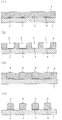
- 1 (1) to 1 (4) are schematic cross-sectional views of a structure including a substrate in each step of a solder electrode manufacturing method according to the present invention.
- 2 (5-1) and (5-2) are schematic cross-sectional views of the laminate according to the present invention.
- the method for producing a solder electrode according to the present invention includes a step (1) of forming a coating film of a photosensitive resin composition on a substrate having an electrode pad, selectively exposing the coating film, and further developing the electrode.
- a method for producing a solder electrode comprising a step (2) of forming a resist having an opening in a region corresponding to a pad and a step (3) of filling the opening with a molten solder, wherein the photosensitive resin composition comprises: And at least a benzoxazole precursor.
- the method for producing a solder electrode of the present invention is different from the conventional method in that the photosensitive resin composition used in the step (1) contains a benzoxazole precursor.
- the operations in the steps (1) to (3) can be performed in the same manner as in the conventional method.
- step (1) a coating film 3 of a photosensitive resin composition is formed on a substrate 1 having electrode pads 2.
- the substrate 1 is, for example, a semiconductor substrate, a glass substrate, a silicon substrate, a substrate formed by providing various metal films on the surface of a semiconductor plate, a glass plate, and a silicon plate.
- the substrate 1 has a large number of electrode pads 2.
- the coating film 3 is formed by applying a photosensitive resin composition to the substrate 1.
- the coating method of the photosensitive resin composition is not particularly limited, and examples thereof include a spray method, a roll coating method, a spin coating method, a slit die coating method, a bar coating method, and an ink jet method.
- the film thickness of the coating film 3 is usually 1 to 500 ⁇ m, preferably 5 to 200 ⁇ m, more preferably 10 to 100 ⁇ m.
- the photosensitive resin composition contains at least a benzoxazole precursor.
- the benzoxazole precursor reacts in the molecule and rapidly changes to a heat-resistant structure.
- the resist formed from the photosensitive resin composition is heated to a high temperature during solder filling such as the IMS method, the benzoxazole precursor contained in the resist rapidly changes to a heat-resistant structure. Therefore, the heat resistance is improved, and as a result, the occurrence of cracks on the resist surface is prevented and the solder embedding property is improved.
- the coating film formed from the photosensitive resin composition is crosslinked by exposure in the step (2) described later.
- the crosslinking agent contained in the photosensitive resin composition is not completely consumed only by exposure, and the crosslinking agent that has not been consumed remains in the resist.
- the resist is not completely cross-linked only by being exposed, and the strength of the resist is not sufficiently increased.
- the resist cannot withstand the heat received from the IMS head, and cracks and dripping are considered to occur. .
- the method for manufacturing a solder electrode according to the present invention as described above, since the heat resistance of the resist is rapidly improved by heating, no cracks or dripping occurs.
- a polybenzoxazole precursor obtained by using dicarboxylic acid and dihydroxydiamine as raw materials is preferably exemplified.
- Such a benzoxazole precursor is obtained by reacting dicarboxylic acid and dihydroxydiamine, and has a structure derived from dicarboxylic acid and a structure derived from dihydroxydiamine, that is, a dicarboxylic acid residue and a dihydroxydiamine residue. Since such a benzoxazole precursor has a structure with particularly high heat resistance when subjected to heat, the resist obtained from the photosensitive resin composition of the present invention containing the benzoxazole precursor is subjected to high heat. In this case, the generation of cracks on the surface can be prevented more effectively.
- dicarboxylic acid examples include isophthalic acid, terephthalic acid, 2,2-bis (4-carboxyphenyl) hexafluoropropane, 4,4′-biphenyldicarboxylic acid, 4,4′-dicarboxydiphenyl ether, 4,4 ′.
- dihydroxydiamine examples include 3,3′-diamino-4,4′-dihydroxybiphenyl, 4,4′-diamino-3,3′-dihydroxybiphenyl, bis (3-amino-4-hydroxyphenyl) propane, bis (4-amino-3-hydroxyphenyl) propane, bis (3-amino-4-hydroxyphenyl) sulfone, bis (4-amino-3-hydroxyphenyl) sulfone, bis (3-amino-4-hydroxyphenyl) hexa Fluoropropane, bis (4-amino-3-hydroxyphenyl) hexafluoropropane, bis (3-amino-4-hydroxyphenyl) propane, bis (4-amino-3-hydroxyphenyl) propane, 4,6-diaminoresorcinol 4,5-diaminoresorcinol, bis (4-amino-3 -Aromatic diamines such as carboxyphenyl) methane.
- the polystyrene-reduced weight average molecular weight (Mw) of the benzoxazole precursor measured by gel permeation chromatography is preferably 3,000 to 200,000, more preferably 5,000 to 100,000.
- the content of the benzoxazole precursor in the photosensitive resin composition is usually 50% by mass or more, preferably 60 to 95% by mass, more preferably 100% by mass when the total solid content in the composition is 100% by mass. Is 70 to 90% by mass.
- the photosensitive resin composition can contain components usually contained in the photosensitive resin composition used in the conventional method.
- the photosensitive resin composition may be a positive type or a negative type. Whether the photosensitive resin composition is positive or negative depends on the type of photosensitive agent contained in the photosensitive resin composition. In the case of positive type, the photosensitive resin composition contains naphthoquinone diazide as an essential component as a photosensitizer, and in the case of negative type, it contains a photoacid generator and a cationic crosslinking agent as essential components as a photosensitizer.
- the coating film containing the naphthoquinone diazide compound is hardly soluble in an alkaline developer, but the naphthoquinone diazide compound is decomposed by irradiation with light to generate a carboxyl group and readily become alkali soluble. Therefore, the coating film containing a naphthoquinone diazide compound changes from hardly alkaline to easily soluble alkali upon irradiation with light.
- the naphthoquinonediazide compound is an ester compound of a compound having one or more phenolic hydroxyl groups and 1,2-naphthoquinonediazide-4-sulfonic acid or 1,2-naphthoquinonediazide-5-sulfonic acid.
- naphthoquinone diazide compound examples include 4,4′-dihydroxydiphenylmethane, 4,4′-dihydroxydiphenyl ether, 2,3,4-trihydroxybenzophenone, 2,3,4,4′-tetrahydroxybenzophenone, 2,3 , 4,2 ′, 4′-pentahydroxybenzophenone, tris (4-hydroxyphenyl) methane, tris (4-hydroxyphenyl) ethane, 1,1-bis (4-hydroxyphenyl) -1-phenylethane, 1, 3-bis [1- (4-hydroxyphenyl) -1-methylethyl] benzene, 1,4-bis [1- (4-hydroxyphenyl) -1-methylethyl] benzene, 4,6-bis [1- (4-Hydroxyphenyl) -1-methylethyl] -1,3-dihydroxybenzene, 1,1-bis 4-hydroxyphenyl) -1- [4- [1- (4-hydroxydip
- the naphthoquinonediazide compound may be used alone or in combination of two or more.
- the photoacid generator is a compound that forms an acid upon light irradiation. Since this acid acts on the cation reactive group of the cationic crosslinking agent to form a crosslinked structure, the coating film containing the photoacid generator and the cationic crosslinking agent is hardly soluble in an alkaline developer by light irradiation. Become.
- Examples of the photoacid generator include onium salt compounds, halogen-containing compounds, sulfone compounds, sulfonic acid compounds, sulfonimide compounds, and diazomethane compounds.
- an onium salt compound and a halogen-containing compound are preferable because a cured film having excellent elongation property can be formed.
- onium salt compounds include iodonium salts, sulfonium salts, phosphonium salts, diazonium salts, and pyridinium salts.
- preferred onium salts include diphenyliodonium trifluoromethanesulfonate, diphenyliodonium p-toluenesulfonate, diphenyliodonium hexafluoroantimonate, diphenyliodonium hexafluorophosphate, diphenyliodonium tetrafluoroborate, triphenylsulfonium trifluorochlorosulfonate, Phenylsulfonium p-toluenesulfonate, triphenylsulfonium hexafluoroantimonate, 4-t-butylphenyl diphenylsulfonium trifluoromethanesulfonate, 4-t-butylphenylpheny
- halogen-containing compound examples include haloalkyl group-containing hydrocarbon compounds and haloalkyl group-containing heterocyclic compounds.
- preferred halogen-containing compounds include 1,10-dibromo-n-decane, 1,1-bis (4-chlorophenyl) -2,2,2-trichloroethane, and phenyl-bis (trichloromethyl) -s-triazine.
- S-triazine derivatives such as 4-methoxyphenyl-bis (trichloromethyl) -s-triazine, styryl-bis (trichloromethyl) -s-triazine, naphthyl-bis (trichloromethyl) -s-triazine, and the like.
- sulfone compounds include ⁇ -ketosulfone compounds, ⁇ -sulfonylsulfone compounds, and ⁇ -diazo compounds of these compounds.
- Specific examples of preferred sulfone compounds include 4-trisphenacylsulfone, mesitylphenacylsulfone, and bis (phenacylsulfonyl) methane.
- sulfonic acid compounds examples include alkyl sulfonic acid esters, haloalkyl sulfonic acid esters, aryl sulfonic acid esters, and imino sulfonates.
- Specific examples of preferred sulfonic acid compounds include benzoin tosylate, pyrogallol tris trifluoromethane sulfonate, o-nitrobenzyl trifluoromethane sulfonate, and o-nitrobenzyl p-toluene sulfonate.
- sulfonimide compound examples include N- (trifluoromethylsulfonyloxy) succinimide, N- (trifluoromethylsulfonyloxy) phthalimide, N- (trifluoromethylsulfonyloxy) diphenylmaleimide, N- (trifluoromethylsulfonyloxy).
- sulfonimide compound examples include N- (trifluoromethylsulfonyloxy) succinimide, N- (trifluoromethylsulfonyloxy) phthalimide, N- (trifluoromethylsulfonyloxy) diphenylmaleimide, N- (trifluoromethylsulfonyloxy).
- Bicyclo [2.2.1] hept-5-ene-2,3-dicarboximide N- (trifluoromethylsulfonyloxy) naphthylimide.
- diazomethane compound examples include bis (trifluoromethylsulfonyl) diazomethane, bis (cyclohexylsulfonyl) diazomethane, and bis (phenylsulfonyl) diazomethane.
- the photoacid generator may be used alone or in combination of two or more.
- the cationic crosslinking agent acts as a crosslinking component (curing component).
- the cationic crosslinking agent include compounds having two or more alkyl etherified amino groups (hereinafter also referred to as “amino group-containing compounds”), oxirane ring-containing compounds, oxetane ring-containing compounds, isocyanate group-containing compounds ( Inclusive), aldehyde group-containing phenol compounds, and methylol group-containing phenol compounds.
- amino group-containing compounds compounds having two or more alkyl etherified amino groups
- oxirane ring-containing compounds oxirane ring-containing compounds
- oxetane ring-containing compounds oxetane ring-containing compounds
- isocyanate group-containing compounds Inclusive
- alkyl etherified amino group examples include a group represented by the following formula.
- R 11 represents a methylene group or an alkylene group
- R 12 represents an alkyl group.
- amino group-containing compounds include active methylol groups (CH 2 OH) in nitrogen compounds such as (poly) methylolated melamine, (poly) methylolated glycoluril, (poly) methylolated benzoguanamine, and (poly) methylolated urea.
- nitrogen compounds such as (poly) methylolated melamine, (poly) methylolated glycoluril, (poly) methylolated benzoguanamine, and (poly) methylolated urea.
- a compound in which part or all (at least two) of the group) is alkyl etherified.
- examples of the alkyl group constituting the alkyl ether include a methyl group, an ethyl group, and a butyl group, and these may be the same as or different from each other.
- the methylol group that is not alkyletherified may be self-condensed within one molecule, or may be condensed between two molecules, and as a result, an oligomer component may be formed.
- an oligomer component may be formed.
- hexamethoxymethyl melamine, hexabutoxymethyl melamine, tetramethoxymethyl glycoluril, tetrabutoxymethyl glycoluril and the like can be used.
- the oxirane ring-containing compound is not particularly limited as long as it contains an oxirane ring in the molecule.
- a phenol novolac epoxy resin, a cresol novolac epoxy resin, a bisphenol epoxy resin, a trisphenol epoxy resin examples thereof include a tetraphenol type epoxy resin, a phenol-xylylene type epoxy resin, a naphthol-xylylene type epoxy resin, a phenol-naphthol type epoxy resin, a phenol-dicyclopentadiene type epoxy resin, an alicyclic epoxy resin, and an aliphatic epoxy resin.
- the oxirane ring-containing compound examples include resorcinol diglycidyl ether, pentaerythritol glycidyl ether, trimethylolpropane polyglycidyl ether, glycerol polyglycidyl ether, phenyl glycidyl ether, neopentyl glycol diglycidyl ether, ethylene / polyethylene glycol diester.
- Examples thereof include glycidyl ether, propylene / polypropylene glycol diglycidyl ether, 1,6-hexanediol diglycidyl ether, sorbitol polyglycidyl ether, propylene glycol diglycidyl ether, and trimethylolpropane triglycidyl ether.
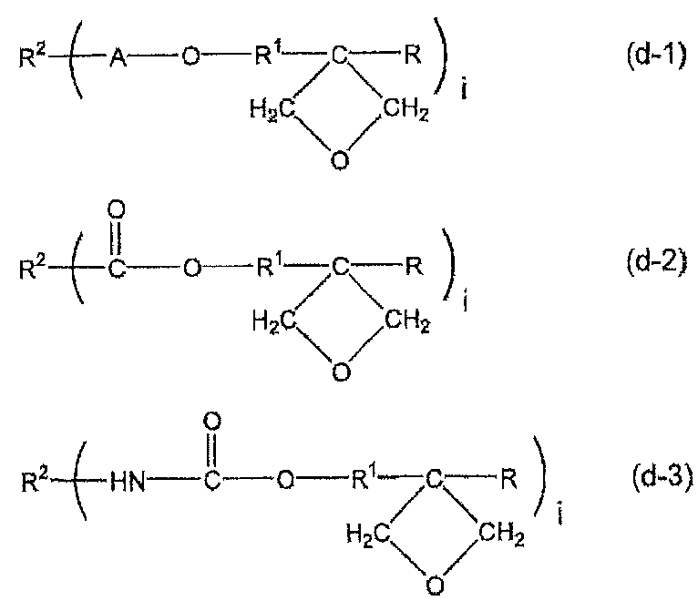
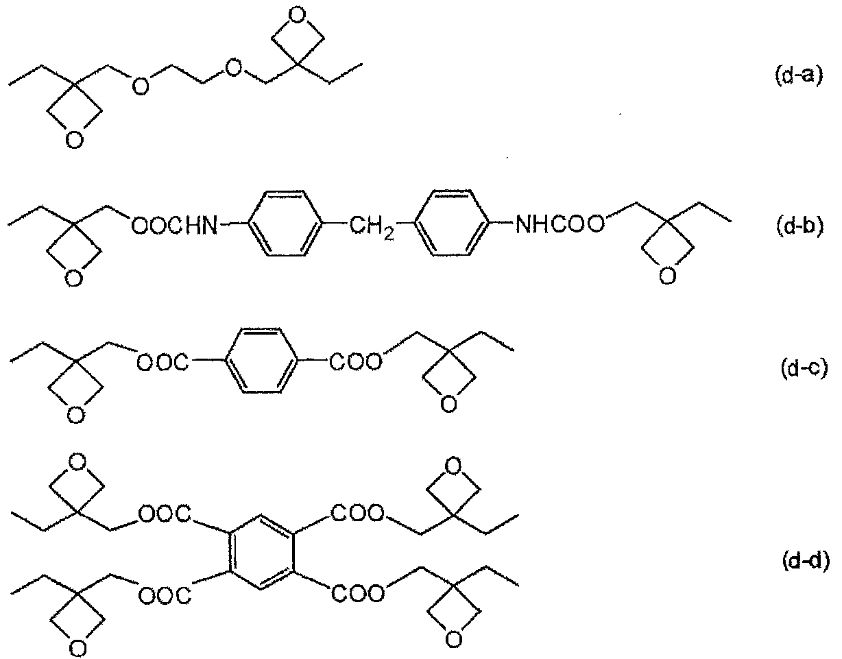
- the oxetane ring-containing compound is not particularly limited as long as it contains an oxetane ring in the molecule, and examples thereof include compounds represented by formulas (d-1) to (d-3).
- A represents a direct bond or an alkylene group such as a methylene group, an ethylene group, or a propylene group;
- R represents an alkyl group such as a methyl group, an ethyl group, or a propyl group.
- R 1 represents an alkylene group such as a methylene group, an ethylene group or a propylene group
- R 2 represents an alkyl group such as a methyl group, an ethyl group, a propyl group or a hexyl group, a phenyl group or a xylyl group
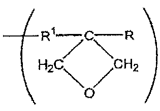
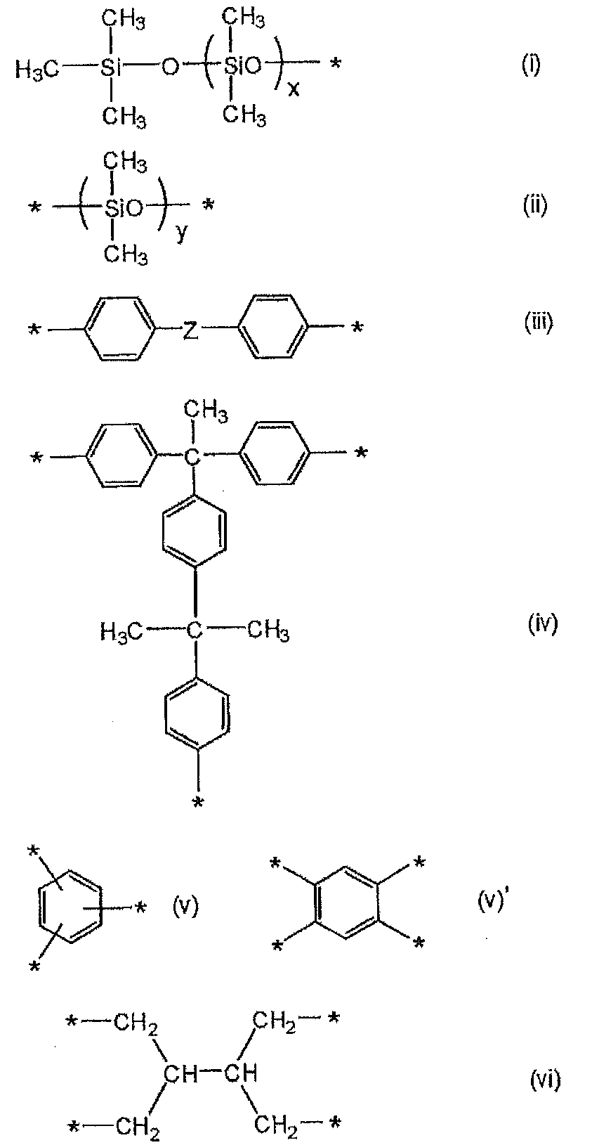
- aryl group a group represented by the following formula (wherein, R and R 1 are each formula (d-1) ⁇ (d -3) are the same as R and R 1 in.),
- “*” represents a binding site.
- x and y are each independently an integer of 0 to 50.
- Z represents a direct bond, or —O—, —CH 2 —, —C (CH 3 ) 2 —, —C (CF 3 ) 2 —, —CO— or —SO 2 —. Divalent group.
- Specific examples of the compounds represented by formulas (d-1) to (d-3) include, for example, 1,4-bis ⁇ [(3-ethyloxetane-3-yl) methoxy] methyl ⁇ benzene (trade name) “OXT-121” manufactured by Toagosei), 3-ethyl-3- ⁇ [(3-ethyloxetane-3-yl) methoxy] methyl ⁇ oxetane (trade name “OXT-221” manufactured by Toagosei) 4,4′-bis [(3-ethyl-3-oxetanyl) methoxymethyl] biphenyl (trade name “ETERRNACOLL OXBP” manufactured by Ube Industries), bis [(3-ethyl-3-oxetanylmethoxy) methyl-phenyl] ether Bis [(3-ethyl-3-oxetanylmethoxy) methyl-phenyl] propane, bis [(3-ethyl
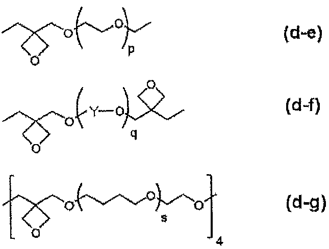
- compounds having a high molecular weight polyvalent oxetane ring can be used.
- examples thereof include oxetane oligomers (trade name “Oligo-OXT”, manufactured by Toagosei Co., Ltd.) and compounds represented by the formulas (de) to (dg).
- p, q and s are each independently an integer of 0 to 10,000, preferably an integer of 1 to 10.
- Y represents an alkylene group such as an ethylene group or a propylene group, or a group represented by —CH 2 —Ph—CH 2 — (wherein Ph represents a phenylene group).
- a cationic crosslinking agent may be used individually by 1 type, and may use 2 or more types together.
- Process (2) In step (2), as shown in FIG. 1 (2), the coating film 3 is selectively exposed and further developed to form a resist 5 having an opening 4 in a region corresponding to each electrode pad 2. To do.
- the coating film 3 is partially exposed so that the openings 4 for accommodating the electrode pads 2 are formed, and then developed to form the openings 4 for accommodating the electrode pads 2. .
- a resist 5 having an opening 4 in a region corresponding to each electrode pad 2 is obtained.
- the opening 4 is a hole that penetrates the resist 5.
- the exposure and development can be performed according to conventional methods.
- the maximum width of the opening 4 is usually 0.1 to 10 times, preferably 0.5 to 2 times the film thickness of the coating film 3. (Process (3))
- the opening 4 is filled with molten solder while heating. After cooling, solder electrodes 6 are formed in the openings 4 as shown in FIG.
- the method of filling the opening 4 while heating the molten solder is not particularly limited, and a normal filling method by the IMS method can be adopted. In the IMS method, filling is usually performed while heating the molten solder at 250 ° C. or higher.
- the photosensitive resin composition contains a benzoxazole precursor that changes to a heat-resistant structure by heat, a high-temperature head is formed as in the IMS method. Even when pressed against the surface of the resist 5 and filled with molten solder, the occurrence of cracks and dripping on the surface of the resist 5 can be suppressed.
- solder electrode manufactured as described above by the method for manufacturing a solder electrode according to the present invention is formed without causing cracks or dripping in the resist, the shape is not disturbed, and the electrode is suitable for the purpose. .
- the method for manufacturing a solder electrode may further include a step (4) of peeling the resist 5 from the substrate 1 after the step (3).
- FIG. 1 (4) shows a state where the resist 5 is peeled off from the substrate 1 after the step (3).
- solder electrode manufactured by the solder electrode manufacturing method of the present invention can be used together with the resist 5 as shown in FIG. 1 (3), or without the resist 5 as shown in FIG. 1 (4). It can also be used.
- the manufacturing method of the 1st laminated body of this invention is the process (1) which forms the coating film of the photosensitive resin composition on the 1st board
- the resin composition contains at least a benzoxazole precursor.
- the manufacturing method of the 2nd laminated body of this invention is the process (1) which forms the coating film of the photosensitive resin composition on the 1st board
- It is a manufacturing method of the laminated body which has the process (5) which forms a general connection structure, Comprising:
- the said photosensitive resin composition contains a benzoxazole precursor at least.
- Steps (1) to (3) in the method for manufacturing the first and second laminates, and step (4) in the method for manufacturing the second laminate are steps (1) to ( 5) and substantially the same. That is, the first laminate manufacturing method is a method of performing the step (5) after the steps (1) to (3) in the solder electrode manufacturing method, and the second laminate manufacturing method is the above-described method. In this method, the step (5) is performed after the steps (1) to (4) in the solder electrode manufacturing method.
- the substrate in the solder electrode manufacturing method corresponds to the first substrate.
- the electrical connection between the electrode pad of the first substrate and the electrode pad of the second substrate having the electrode pad is performed via the solder electrode.
- Step (5) of forming a general connection structure is performed.
- FIG. 2 (5-1) shows the laminate 10 produced by the first laminate production method.
- the laminate 10 has the electrode pad 2 of the first substrate 1 and the electrode pad 12 through the solder electrode 6 in the state shown in FIG. 1 (3) manufactured by the steps (1) to (3). It has an electrical connection structure formed by connecting the electrode pads 12 of the second substrate 11.
- the electrode pad 12 of the second substrate 11 faces the electrode pad 2 of the first substrate 1 when the first substrate 1 and the second substrate 11 are opposed to each other with the surfaces on which the electrode pads are formed facing each other. In the position.
- the electrode pad 12 of the second substrate 11 is brought into contact with the solder electrode 6 in the state shown in FIG. 12 are electrically connected to each other through the solder electrode 6 to form an electrical connection structure, whereby the laminate 10 is obtained.
- the heating temperature is usually 100 to 300 ° C.
- the force during the pressure bonding is usually 0.1 to 10 MPa.
- the stacked body 10 includes the first substrate 1, the solder electrode 6, the second substrate 11, and the first substrate 1. And a resist 5 sandwiched between the substrate 1 and the second substrate 11.
- the electrical connection between the electrode pad of the first substrate and the electrode pad of the second substrate having the electrode pad is performed via the solder electrode.
- Step (5) of forming a general connection structure is performed.
- FIG. 2 (5-2) shows the laminate 20 produced by the second laminate production method.
- the laminated body 20 has the electrode pad 2 of the first substrate 1 and the electrode pad 12 through the solder electrode 6 in the state shown in FIG. 1 (4) manufactured by the steps (1) to (4). It has an electrical connection structure formed by connecting the electrode pads 12 of the second substrate 11.
- the electrode pads 12 of the second substrate 11 are brought into contact with the solder electrodes 6 in the state shown in FIG. 1 (4), and heated and / or pressed to form the electrode pads 2 of the first substrate 1 and the electrode pads of the second substrate 11. 12 are electrically connected to each other through the solder electrode 6 to form an electrical connection structure, whereby the laminate 20 is obtained.
- the stacked body 20 is formed of the first substrate 1, the solder electrode 6, and the second substrate 11.
- the laminate produced by the laminate production method of the present invention may or may not include a resist between the first substrate and the second substrate.
- the resist is used as an underfill.
- the laminate manufactured by the method for manufacturing a laminate of the present invention has an electrical connection structure suitable for the purpose by the IMS method, the selectivity of the solder composition is widened, so that the semiconductor element, the display element, and the power device It is applicable to various electronic parts such as.
- the laminate produced by the laminate production method of the present invention can be used for electronic components such as semiconductor elements, display elements, and power devices.
- the reaction solution was dropped into a large amount of cyclohexane to solidify the reaction product.
- the coagulated product was washed with water, and the coagulated product was redissolved in tetrahydrofuran having the same mass as the coagulated product, and then the obtained solution was dropped into a large amount of cyclohexane to coagulate again.
- the obtained coagulated product was vacuum dried at 40 ° C. for 48 hours to obtain an alkali-soluble resin.
- the weight average molecular weight of the alkali-soluble resin was 10,000.
- photosensitive resin composition 1 100 parts of the polybenzoxazole precursor synthesized in Synthesis Example 1 and 1,1-bis (4-hydroxyphenyl) -1- [4- [1- ( 10 parts of a condensate of 4-hydroxyphenyl) -1-methylethyl] phenyl] ethane and 1,2-naphthoquinonediazide-5-sulfonic acid (molar ratio of the latter to the former: 2.0), N-methyl- Using 100 parts of 2-pyrrolidone, these were mixed and stirred to obtain a uniform solution. This solution was filtered through a capsule filter having a pore diameter of 10 ⁇ m to prepare a photosensitive resin composition 1.
- Preparation Example 1 Preparation of photosensitive resin composition 2 100 parts of the alkali-soluble resin synthesized in Synthesis Example 2 above, 50 parts of polyester acrylate (trade name “Aronix M-8060” manufactured by Toagosei Co., Ltd.), 4 parts of diphenyl (2,4,6-trimethylbenzoyl) phosphine oxide (trade name “LUCIRIN TPO”, manufactured by BASF Corp.), 2,2-dimethoxy-1,2-diphenylethane-1-one (trade name) 19 parts of “IRGACURE 651” (manufactured by BASF Corporation) and 80 parts of propylene glycol monomethyl ether acetate were mixed and stirred to obtain a uniform solution. This solution was filtered through a capsule filter having a pore diameter of 10 ⁇ m to prepare a photosensitive resin composition 2.
- polyester acrylate trade name “Aronix M-8060” manufactured by Toagosei Co., Ltd.
- Example 2 The photosensitive resin composition 1 prepared in Example 1 was applied onto a substrate having a plurality of copper electrode pads on a silicon plate using a spin coater, heated at 120 ° C. for 5 minutes on a hot plate, A coating film having a thickness of 20 ⁇ m was formed. Next, using an aligner (manufactured by Suss, model “MA-200”), the coating film was exposed to light having a wavelength of 420 nm through a pattern mask at an irradiation intensity of 300 mJ / cm 2 .
- an aligner manufactured by Suss, model “MA-200
- the coating film After the exposure, the coating film is brought into contact with a 2.38 mass% tetramethylammonium hydroxide aqueous solution for 240 seconds, the coating film is washed with running water, developed, and a resist holding substrate having an opening corresponding to the electrode pad is formed. did.
- the opening of each opening was circular with a diameter of 30 ⁇ m, and the depth of each opening was 20 ⁇ m. The maximum width of the opening was 30 ⁇ m.
- the resist holding substrate having the opening was immersed in a 1% by mass sulfuric acid aqueous solution at 23 ° C. for 1 minute, washed with water and dried.
- a molten solder obtained by melting SAC305 (product name, lead-free solder, Senju Metal Industry Co., Ltd.) at 250 ° C. was filled in the opening of the substrate after drying over 10 minutes while heating to 250 ° C. .
- SAC305 product name, lead-free solder, Senju Metal Industry Co., Ltd.
- the resist holding substrate on which the solder electrode is formed is immersed in a solution obtained by mixing 90 parts of dimethyl sulfoxide, 3 parts of tetramethylammonium hydroxide and 7 parts of water at 50 ° C. for 20 minutes, and the resist is removed from the substrate. Was peeled off.
- substrate provided with the obtained solder electrode was washed with water and dried.
- substrate which has another copper electrode pad was mounted in the board
- a pressure of 0.3 MPa at 250 ° C. is applied for 30 seconds to the substrate having the two copper electrode pads so that they are pressed together, and the substrate having the copper electrode pad, the solder electrode, the copper electrode pad.
- substrate which has was manufactured. When this laminated body was observed with an electron microscope, it was confirmed that the laminated body had an appropriate electrical connection structure.
- the coating film After the exposure, the coating film is brought into contact with a 2.38 mass% tetramethylammonium hydroxide aqueous solution for 240 seconds, the coating film is washed with running water, developed, and a resist holding substrate having an opening corresponding to the electrode pad is formed. did.
- the opening of each opening was circular with a diameter of 30 ⁇ m, and the depth of each opening was 20 ⁇ m. The maximum width of the opening was 30 ⁇ m.
- the resist holding substrate having the opening was immersed in a 1% by mass sulfuric acid aqueous solution at 23 ° C. for 1 minute, washed with water and dried.
- a molten solder obtained by melting SAC305 (product name, lead-free solder, Senju Metal Industry Co., Ltd.) at 250 ° C. was filled in the opening of the substrate after drying over 10 minutes while heating to 250 ° C. .
- substrate after molten solder filling was observed with the electron microscope, it confirmed that the crack had generate
Landscapes
- Engineering & Computer Science (AREA)
- Physics & Mathematics (AREA)
- Manufacturing & Machinery (AREA)
- Microelectronics & Electronic Packaging (AREA)
- General Physics & Mathematics (AREA)
- Spectroscopy & Molecular Physics (AREA)
- Mechanical Engineering (AREA)
- Materials For Photolithography (AREA)
- Photosensitive Polymer And Photoresist Processing (AREA)
- Non-Metallic Protective Coatings For Printed Circuits (AREA)
- Electric Connection Of Electric Components To Printed Circuits (AREA)
Abstract
Description
前記感光性樹脂組成物は、少なくともベンゾオキサゾール前駆体を含有することを特徴とする。
前記感光性樹脂組成物は、少なくともベンゾオキサゾール前駆体を含有することを特徴とする。
前記感光性樹脂組成物は、少なくともベンゾオキサゾール前駆体を含有することを特徴とする。
本発明のはんだ電極の製造方法は、電極パッドを有する基板上に感光性樹脂組成物の塗膜を形成する工程(1)、前記塗膜を選択的に露光し、さらに現像することにより、電極パッドに対応する領域に開口部を有するレジストを形成する工程(2)、前記開口部に溶融はんだを充填する工程(3)を有するはんだ電極の製造方法であって、前記感光性樹脂組成物は、少なくともベンゾオキサゾール前駆体を含有することを特徴とする。
(工程(1))
工程(1)では、図1(1)に示すように、電極パッド2を有する基板1上に感光性樹脂組成物の塗膜3を形成する。

アミノ基含有化合物としては、例えば、(ポリ)メチロール化メラミン、(ポリ)メチロール化グリコールウリル、(ポリ)メチロール化ベンゾグアナミン、(ポリ)メチロール化ウレア等の窒素化合物中の活性メチロール基(CH2OH基)の一部または全部(少なくとも2個)がアルキルエーテル化された化合物が挙げられる。ここで、アルキルエーテルを構成するアルキル基としては、例えば、メチル基、エチル基、ブチル基が挙げられ、これらは互いに同一であってもよいし、異なっていてもよい。また、アルキルエーテル化されていないメチロール基は、一分子内で自己縮合していてもよく、二分子間で縮合して、その結果、オリゴマー成分が形成されていてもよい。具体的には、ヘキサメトキシメチルメラミン、ヘキサブトキシメチルメラミン、テトラメトキシメチルグリコールウリル、テトラブトキシメチルグリコールウリル等を用いることができる。
(工程(2))
工程(2)では、図1(2)に示すように、塗膜3を選択的に露光し、さらに現像することにより、各電極パッド2に対応する領域に開口部4を有するレジスト5を形成する。
(工程(3))
工程(3)では、開口部4に溶融はんだを加熱しながら充填する。冷却後、図1(3)に示すように、各開口部4にはんだ電極6が形成される。
本発明の第1の積層体の製造方法は、電極パッドを有する第1基板上に感光性樹脂組成物の塗膜を形成する工程(1)、前記塗膜を選択的に露光し、さらに現像することにより、電極パッドに対応する領域に開口部を有するレジストを形成する工程(2)、前記開口部に溶融はんだを加熱しながら充填して、はんだ電極を形成する工程(3)、前記はんだ電極を介して、前記第1基板の電極パッドと電極パッドを有する第2基板の電極パッドとの電的接続構造を形成する工程(5)を有する積層体の製造方法であって、前記感光性樹脂組成物は、少なくともベンゾオキサゾール前駆体を含有する。
1.物性の測定方法
(ポリベンゾオキサゾール前駆体およびアルカリ可溶性樹脂の重量平均分子量(Mw)の測定方法)
下記条件下でゲルパーミエーションクロマトグラフィー法にてポリベンゾオキサゾール前駆体およびアルカリ可溶性樹脂の重量平均分子量(Mw)を測定した。
・カラム:東ソー社製カラムのTSK-MおよびTSK2500を直列に接続
・溶媒:テトラヒドロフラン
・温度:40℃
・検出方法:屈折率法
・標準物質:ポリスチレン
・GPC装置:東ソー製、装置名「HLC-8220-GPC」
[合成例1]ポリベンゾオキサゾール前駆体の合成
フラスコ中に、イソフタル酸20g およびN-メチルピロリドン100g を入れ、フラスコ内容物を5 ℃ に冷却した後、塩化チオニル29g を滴下し、30分間反応させて、イソフタル酸クロリドの溶液を得た。
窒素置換した、ドライアイス/メタノール還流器の付いたフラスコ中に、重合開始剤として2,2'-アゾビスイソブチロニトリル5.0g、および重合溶媒としてジエチレングリコールエチルメチルエーテル90gを入れ、攪拌した。得られた溶液に、メタクリル酸10g、p-イソプロペニルフェノール15g、トリシクロ〔5.2.1.02,6〕デカニルメタクリレート25g、イソボルニルアクリレート20g、およびn-ブチルアクリレート30gを加え、攪拌を開始し、80℃まで昇温した。その後、80℃で6時間加熱し、反応を行った。
前記合成例1で合成したポリベンゾオキサゾール前駆体を100部、1,1-ビス(4-ヒドロキシフェニル)-1-[4-[1-(4-ヒドロキシフェニル)-1-メチルエチル]フェニル]エタンと1,2-ナフトキノンジアジド-5-スルホン酸との縮合物(前者に対する後者のモル比:2.0)を10部、N-メチル-2-ピロリドンを100部用い、これらを混合、攪拌して均一な溶液を得た。この溶液を、孔径10μmのカプセルフィルターでろ過して、感光性樹脂組成物1を調製した。
前記合成例2で合成したアルカリ可溶性樹脂を100部、ポリエステルアクリレート(商品名「アロニックスM-8060」、東亞合成(株)製)を50部、ジフェニル(2,4,6-トリメチルベンゾイル)ホスフィンオキシド(商品名「LUCIRIN TPO」、BASF(株)製)を4部、2,2-ジメトキシ-1,2-ジフェニルエタン-1-オン(商品名「IRGACURE 651」、BASF(株)製)を19部、プロピレングリコールモノメチルエーテルアセテートを80部用い、これらを混合、攪拌して均一な溶液を得た。この溶液を、孔径10μmのカプセルフィルターでろ過して、感光性樹脂組成物2を調製した。
シリコン板上に複数の銅電極パッドを有する基板上に、スピンコーターを用いて、実施例1で調製した感光性樹脂組成物1を塗布し、ホットプレートで120℃にて5分間加熱し、厚さ20μmの塗膜を形成した。次いでアライナー(Suss社製、型式「MA-200」)を用い、この塗膜に、パターンマスクを介して波長420nmの光を照射強度300mJ/cm2にて露光した。露光後、塗膜を2.38質量%テトラメチルアンモニウムハイドロオキサイド水溶液に240秒間接触させ、塗膜を流水で洗浄し、現像し、電極パッドに対応する部分に開口部を有するレジスト保持基板を形成した。電子顕微鏡で観察したところ、各開口部の開口は直径30μmの円形であり、各開口部の深さは20μmであった。また、開口部の最大幅は30μmであった。
シリコン板上に複数の銅電極パッドを有する基板上にスピンコーターを用いて、調製例1で調製した感光性樹脂組成物2を塗布し、ホットプレートで120℃にて5分間加熱し、厚さ20μmの塗膜を形成した。次いでアライナー(Suss社製、型式「MA-200」)を用い、この塗膜に、パターンマスクを介して、波長420nmの光を照射強度300mJ/cm2にて露光した。露光後、塗膜を2.38質量%テトラメチルアンモニウムハイドロオキサイド水溶液に240秒間接触させ、塗膜を流水で洗浄し、現像し、電極パッドに対応する部分に開口部を有するレジスト保持基板を形成した。電子顕微鏡で観察したところ、各開口部の開口は直径30μmの円形であり、各開口部の深さは20μmであった。また、開口部の最大幅は30μmであった。
2、12 電極パッド
3 塗膜
4 開口部
5 レジスト
6 はんだ電極
10、20 積層体
Claims (13)
- 電極パッドを有する基板上に感光性樹脂組成物の塗膜を形成する工程(1)、前記塗膜を選択的に露光し、さらに現像することにより、電極パッドに対応する領域に開口部を有するレジストを形成する工程(2)、前記開口部に溶融はんだを充填する工程(3)を有するはんだ電極の製造方法であって、
前記感光性樹脂組成物は、少なくともベンゾオキサゾール前駆体を含有することを特徴とするはんだ電極の製造方法。 - 前記ベンゾオキサゾール前駆体が、ジカルボン酸を由来とする構造及びジヒドロキシジアミンを由来とする構造を有する請求項1に記載のはんだ電極の製造方法。
- 前記ジカルボン酸が、芳香族系ジカルボン酸である請求項2に記載のはんだ電極の製造方法。
- 前記ジヒドロキシジアミンが、芳香族系ジアミンである請求項2または3に記載のはんだ電極の製造方法。
- 前記感光性樹脂組成物がさらに感光剤を含有する、請求項1~4のいずれかに記載のはんだ電極の製造方法。
- 前記感光剤がナフトキノンジアジド化合物である、請求項5に記載のはんだ電極の製造方法。
- さらに、前記レジストを剥離する工程(4)を有する請求項1~6のいずれかに記載のはんだ電極の製造方法。
- 請求項1~7のいずれかに記載のはんだ電極の製造方法によって製造したはんだ電極。
- 電極パッドを有する第1基板上に感光性樹脂組成物の塗膜を形成する工程(1)、前記塗膜を選択的に露光し、さらに現像することにより、電極パッドに対応する領域に開口部を有するレジストを形成する工程(2)、前記開口部に溶融はんだを加熱しながら充填して、はんだ電極を形成する工程(3)、前記はんだ電極を介して、前記第1基板の電極パッドと電極パッドを有する第2基板の電極パッドとの電的接続構造を形成する工程(5)を有する積層体の製造方法であって、
前記感光性樹脂組成物は、少なくともベンゾオキサゾール前駆体を含有することを特徴とする積層体の製造方法。 - 電極パッドを有する第1基板上に感光性樹脂組成物の塗膜を形成する工程(1)、前記塗膜を選択的に露光し、さらに現像することにより、電極パッドに対応する領域に開口部を有するレジストを形成する工程(2)、前記開口部に溶融はんだを加熱しながら充填して、はんだ電極を形成する工程(3)、工程(3)の後、前記レジストを剥離する工程(4)、工程(4)の後、前記はんだ電極を介して、前記第1基板の電極パッドと電極パッドを有する第2基板の電極パッドとの電的接続構造を形成する工程(5)を有する積層体の製造方法であって、
前記感光性樹脂組成物は、少なくともベンゾオキサゾール前駆体を含有することを特徴とする積層体の製造方法。 - 請求項9又は10のいずれかに記載の積層体の製造方法によって製造した積層体。
- 請求項11に記載の積層体を有する電子部品。
- 少なくともベンゾオキサゾール前駆体を含有する射出成形はんだ用感光性樹脂組成物。
Priority Applications (4)
| Application Number | Priority Date | Filing Date | Title |
|---|---|---|---|
| CN201680026329.2A CN107533991A (zh) | 2015-05-08 | 2016-04-28 | 焊料电极的制造方法及其用途 |
| KR1020177030457A KR20180005163A (ko) | 2015-05-08 | 2016-04-28 | 땜납 전극의 제조 방법 및 그의 용도 |
| JP2017517887A JPWO2016181859A1 (ja) | 2015-05-08 | 2016-04-28 | はんだ電極の製造方法およびその用途 |
| US15/572,163 US20180129134A1 (en) | 2015-05-08 | 2016-04-28 | Production process for solder electrode and use thereof |
Applications Claiming Priority (2)
| Application Number | Priority Date | Filing Date | Title |
|---|---|---|---|
| JP2015095670 | 2015-05-08 | ||
| JP2015-095670 | 2015-05-08 |
Publications (1)
| Publication Number | Publication Date |
|---|---|
| WO2016181859A1 true WO2016181859A1 (ja) | 2016-11-17 |
Family
ID=57248867
Family Applications (1)
| Application Number | Title | Priority Date | Filing Date |
|---|---|---|---|
| PCT/JP2016/063365 Ceased WO2016181859A1 (ja) | 2015-05-08 | 2016-04-28 | はんだ電極の製造方法およびその用途 |
Country Status (6)
| Country | Link |
|---|---|
| US (1) | US20180129134A1 (ja) |
| JP (1) | JPWO2016181859A1 (ja) |
| KR (1) | KR20180005163A (ja) |
| CN (1) | CN107533991A (ja) |
| TW (1) | TWI681474B (ja) |
| WO (1) | WO2016181859A1 (ja) |
Cited By (1)
| Publication number | Priority date | Publication date | Assignee | Title |
|---|---|---|---|---|
| JP2022501808A (ja) * | 2018-09-20 | 2022-01-06 | インターナショナル・ビジネス・マシーンズ・コーポレーションInternational Business Machines Corporation | ハイブリッド・アンダーバンプ金属化コンポーネント |
Citations (3)
| Publication number | Priority date | Publication date | Assignee | Title |
|---|---|---|---|---|
| JP2002203869A (ja) * | 2000-10-30 | 2002-07-19 | Seiko Epson Corp | バンプの形成方法、半導体装置及びその製造方法、回路基板並びに電子機器 |
| JP2006056939A (ja) * | 2004-08-18 | 2006-03-02 | Sumitomo Electric Ind Ltd | 熱可塑性フッ素化ポリベンゾオキサゾール樹脂、その前駆体、成形体、これらの製造方法、及び樹脂組成物 |
| JP2012086531A (ja) * | 2010-10-22 | 2012-05-10 | Mitsubishi Materials Corp | はんだペースト印刷用マスクおよびその製造方法、はんだペースト印刷用装置 |
Family Cites Families (9)
| Publication number | Priority date | Publication date | Assignee | Title |
|---|---|---|---|---|
| US7410833B2 (en) * | 2004-03-31 | 2008-08-12 | International Business Machines Corporation | Interconnections for flip-chip using lead-free solders and having reaction barrier layers |
| JP4487191B2 (ja) * | 2004-12-24 | 2010-06-23 | カシオ計算機株式会社 | 画像処理装置および画像処理プログラム |
| US7410090B2 (en) * | 2006-04-21 | 2008-08-12 | International Business Machines Corporation | Conductive bonding material fill techniques |
| US8298747B2 (en) * | 2007-03-12 | 2012-10-30 | Hitachi Chemical Dupont Microsystems, Ltd. | Photosensitive resin composition, process for producing patterned hardened film with use thereof and electronic part |
| US8492262B2 (en) * | 2010-02-16 | 2013-07-23 | International Business Machines Corporation | Direct IMS (injection molded solder) without a mask for forming solder bumps on substrates |
| AU2011240695A1 (en) * | 2010-04-12 | 2012-11-01 | Google Inc. | Real-time collaboration in a hosted word processor |
| JP5955036B2 (ja) * | 2012-03-06 | 2016-07-20 | 株式会社タムラ製作所 | はんだバンプの形成方法 |
| JP2014082359A (ja) * | 2012-10-17 | 2014-05-08 | Olympus Corp | 半導体基板、半導体装置、および固体撮像装置、並びに半導体基板の製造方法 |
| US20160003565A1 (en) * | 2014-04-07 | 2016-01-07 | Klint McLean KINGSBURY | Post Barrel Plenum Operated Gas Cycling System for Automatic Firearms |
-
2016
- 2016-04-22 TW TW105112583A patent/TWI681474B/zh not_active IP Right Cessation
- 2016-04-28 KR KR1020177030457A patent/KR20180005163A/ko not_active Withdrawn
- 2016-04-28 WO PCT/JP2016/063365 patent/WO2016181859A1/ja not_active Ceased
- 2016-04-28 US US15/572,163 patent/US20180129134A1/en not_active Abandoned
- 2016-04-28 CN CN201680026329.2A patent/CN107533991A/zh active Pending
- 2016-04-28 JP JP2017517887A patent/JPWO2016181859A1/ja active Pending
Patent Citations (3)
| Publication number | Priority date | Publication date | Assignee | Title |
|---|---|---|---|---|
| JP2002203869A (ja) * | 2000-10-30 | 2002-07-19 | Seiko Epson Corp | バンプの形成方法、半導体装置及びその製造方法、回路基板並びに電子機器 |
| JP2006056939A (ja) * | 2004-08-18 | 2006-03-02 | Sumitomo Electric Ind Ltd | 熱可塑性フッ素化ポリベンゾオキサゾール樹脂、その前駆体、成形体、これらの製造方法、及び樹脂組成物 |
| JP2012086531A (ja) * | 2010-10-22 | 2012-05-10 | Mitsubishi Materials Corp | はんだペースト印刷用マスクおよびその製造方法、はんだペースト印刷用装置 |
Cited By (3)
| Publication number | Priority date | Publication date | Assignee | Title |
|---|---|---|---|---|
| JP2022501808A (ja) * | 2018-09-20 | 2022-01-06 | インターナショナル・ビジネス・マシーンズ・コーポレーションInternational Business Machines Corporation | ハイブリッド・アンダーバンプ金属化コンポーネント |
| US11749605B2 (en) | 2018-09-20 | 2023-09-05 | International Business Machines Corporation | Hybrid under-bump metallization component |
| JP7536000B2 (ja) | 2018-09-20 | 2024-08-19 | インターナショナル・ビジネス・マシーンズ・コーポレーション | ハイブリッド・アンダーバンプ金属化コンポーネント |
Also Published As
| Publication number | Publication date |
|---|---|
| JPWO2016181859A1 (ja) | 2018-02-22 |
| CN107533991A (zh) | 2018-01-02 |
| TWI681474B (zh) | 2020-01-01 |
| KR20180005163A (ko) | 2018-01-15 |
| US20180129134A1 (en) | 2018-05-10 |
| TW201642367A (zh) | 2016-12-01 |
Similar Documents
| Publication | Publication Date | Title |
|---|---|---|
| JP5987984B2 (ja) | 樹脂組成物、感光性樹脂組成物、絶縁膜およびその製法ならびに電子部品 | |
| JP5240380B1 (ja) | 樹脂組成物、重合体、硬化膜および電子部品 | |
| TWI403835B (zh) | 感光性絕緣樹脂組成物及其硬化物以及具備其之電路基板 | |
| JP5077023B2 (ja) | 接着方法およびそれに用いられるポジ型感光性接着剤組成物、並びに電子部品 | |
| US9541827B2 (en) | Photosensitive composition, cured film and production process thereof, and electronic part | |
| JP5444813B2 (ja) | 感光性絶縁樹脂組成物および絶縁膜 | |
| JP5035240B2 (ja) | 感放射線性絶縁樹脂組成物 | |
| US20120296053A1 (en) | Photosensitive composition, cured film and electronic part | |
| JPWO2008117619A1 (ja) | 感光性絶縁樹脂組成物 | |
| JP5176768B2 (ja) | ポジ型感光性絶縁樹脂組成物 | |
| CN110297398A (zh) | 感光树脂组合物、感光树脂层合体和图案形成方法 | |
| TW200811592A (en) | Photosensitive resin composition | |
| TW201335703A (zh) | 感光性樹脂組成物、圖案硬化膜的製造方法以及電子部件 | |
| JP5293877B1 (ja) | 樹脂組成物、重合体、硬化膜および電子部品 | |
| JP5531617B2 (ja) | 電極形成方法及び電極 | |
| WO2016181859A1 (ja) | はんだ電極の製造方法およびその用途 | |
| JP6597243B2 (ja) | はんだ電極の製造方法およびその用途 | |
| JP5369420B2 (ja) | 絶縁膜形成用感光性樹脂組成物 | |
| JP7191622B2 (ja) | 感光性樹脂組成物、ドライフィルム、硬化物、および電子部品 | |
| JP2010205807A (ja) | 被覆層形成方法 | |
| JP6270024B2 (ja) | 感光性接着剤組成物、それを用いる半導体装置の製造方法、及び半導体装置 | |
| JP7312536B2 (ja) | 感光性樹脂組成物、ドライフィルム、硬化物、および電子部品 | |
| JP2022144173A (ja) | 構造体の製造方法 | |
| WO2019146428A1 (ja) | はんだ電極の製造方法およびその用途 | |
| JP2018156030A (ja) | 感光性樹脂組成物、感光性エレメント、半導体装置及びレジストパターンの形成方法 |
Legal Events
| Date | Code | Title | Description |
|---|---|---|---|
| 121 | Ep: the epo has been informed by wipo that ep was designated in this application |
Ref document number: 16792584 Country of ref document: EP Kind code of ref document: A1 |
|
| ENP | Entry into the national phase |
Ref document number: 2017517887 Country of ref document: JP Kind code of ref document: A |
|
| ENP | Entry into the national phase |
Ref document number: 20177030457 Country of ref document: KR Kind code of ref document: A |
|
| WWE | Wipo information: entry into national phase |
Ref document number: 15572163 Country of ref document: US |
|
| NENP | Non-entry into the national phase |
Ref country code: DE |
|
| 122 | Ep: pct application non-entry in european phase |
Ref document number: 16792584 Country of ref document: EP Kind code of ref document: A1 |