WO2016174868A1 - 熱可塑性液晶ポリマーフィルム及び回路基板 - Google Patents
熱可塑性液晶ポリマーフィルム及び回路基板 Download PDFInfo
- Publication number
- WO2016174868A1 WO2016174868A1 PCT/JP2016/002205 JP2016002205W WO2016174868A1 WO 2016174868 A1 WO2016174868 A1 WO 2016174868A1 JP 2016002205 W JP2016002205 W JP 2016002205W WO 2016174868 A1 WO2016174868 A1 WO 2016174868A1
- Authority
- WO
- WIPO (PCT)
- Prior art keywords
- liquid crystal
- crystal polymer
- polymer film
- thermoplastic liquid
- conductor layer
- Prior art date
- Legal status (The legal status is an assumption and is not a legal conclusion. Google has not performed a legal analysis and makes no representation as to the accuracy of the status listed.)
- Ceased
Links
Images

Classifications
-
- B—PERFORMING OPERATIONS; TRANSPORTING
- B32—LAYERED PRODUCTS
- B32B—LAYERED PRODUCTS, i.e. PRODUCTS BUILT-UP OF STRATA OF FLAT OR NON-FLAT, e.g. CELLULAR OR HONEYCOMB, FORM
- B32B15/00—Layered products comprising a layer of metal
- B32B15/04—Layered products comprising a layer of metal comprising metal as the main or only constituent of a layer, which is next to another layer of the same or of a different material
- B32B15/08—Layered products comprising a layer of metal comprising metal as the main or only constituent of a layer, which is next to another layer of the same or of a different material of synthetic resin
-
- C—CHEMISTRY; METALLURGY
- C08—ORGANIC MACROMOLECULAR COMPOUNDS; THEIR PREPARATION OR CHEMICAL WORKING-UP; COMPOSITIONS BASED THEREON
- C08J—WORKING-UP; GENERAL PROCESSES OF COMPOUNDING; AFTER-TREATMENT NOT COVERED BY SUBCLASSES C08B, C08C, C08F, C08G or C08H
- C08J5/00—Manufacture of articles or shaped materials containing macromolecular substances
- C08J5/18—Manufacture of films or sheets
-
- H—ELECTRICITY
- H05—ELECTRIC TECHNIQUES NOT OTHERWISE PROVIDED FOR
- H05K—PRINTED CIRCUITS; CASINGS OR CONSTRUCTIONAL DETAILS OF ELECTRIC APPARATUS; MANUFACTURE OF ASSEMBLAGES OF ELECTRICAL COMPONENTS
- H05K1/00—Printed circuits
- H05K1/02—Details
- H05K1/03—Use of materials for the substrate
-
- H—ELECTRICITY
- H05—ELECTRIC TECHNIQUES NOT OTHERWISE PROVIDED FOR
- H05K—PRINTED CIRCUITS; CASINGS OR CONSTRUCTIONAL DETAILS OF ELECTRIC APPARATUS; MANUFACTURE OF ASSEMBLAGES OF ELECTRICAL COMPONENTS
- H05K3/00—Apparatus or processes for manufacturing printed circuits
- H05K3/38—Improvement of the adhesion between the insulating substrate and the metal
Definitions
- the present invention relates to a thermoplastic liquid crystal polymer film (hereinafter sometimes referred to as a thermoplastic liquid crystal polymer film or simply a liquid crystal polymer film) and a circuit board that form an optically anisotropic molten layer.
- a thermoplastic liquid crystal polymer film hereinafter sometimes referred to as a thermoplastic liquid crystal polymer film or simply a liquid crystal polymer film
- a circuit board that form an optically anisotropic molten layer.
- Transmission loss of high-frequency signals involves dielectric loss in addition to conductor loss. Therefore, in order to suppress the transmission loss of high-frequency signals and improve the information processing speed, that is, the signal propagation speed, there is a demand for an electrically insulating substrate material having excellent dielectric characteristics.
- thermocompression bonding using a thermoplastic liquid crystal polymer film having a dielectric loss smaller than that of a polyimide film as an insulating substrate has attracted attention. ing.
- peel strength peel strength or adhesive strength
- mechanical bonding which is an anchor effect due to the surface roughness of the conductor layer
- the conductor layer surface treatment component A chemical bond, which is a resin bond, is conceivable.
- the anchor effect is enhanced by forming irregularities on the conductor layer, and the treatment to ensure the peel strength when the conductor layer and the insulating layer are crimped is performed. Shape optimization has been studied.
- Patent Document 1 International Publication WO2012 / 020818 Pamphlet
- a metal-clad laminated substrate having a metal foil on one or both sides of a liquid crystal polymer layer the metal foil is roughened on the surface in contact with the liquid crystal polymer layer.
- a metal-clad laminate having protrusions on the surface layer is disclosed.
- the aspect ratio (H / L) represented by the ratio of the height H of the protrusion to the width L of the root portion of the protrusion is in the range of 3 to 20, and the height of the protrusion is 0.1 to It is disclosed that the liquid crystal polymer layer has a thickness of 10 to 2000 ⁇ m and a film thickness tolerance of less than 6%.
- thermoplastic liquid crystal polymer film that can provide high peel strength even when laminated with a conductor layer having excellent high frequency characteristics and low surface roughness.
- a first object of the present invention is to provide a thermoplastic liquid crystal polymer film having a specific toughness that gives high peel strength even when it is thermocompression bonded to an adherend such as a conductor layer having a low surface roughness. is there.
- the second object of the present invention is to provide a thermoplastic liquid crystal having a specific toughness and a specific Young's modulus that gives a high peel strength even when it is thermocompression bonded to an adherend such as a conductor layer having a low surface roughness. It is to provide a polymer film.
- a third object of the present invention is to provide a thermoplastic liquid crystal polymer film that maintains a specific toughness with a low rate of decrease in toughness even after thermocompression bonding with an adherend such as a conductor layer.
- the fourth object of the present invention is to provide a circuit board formed by pressure-bonding the thermoplastic liquid crystal polymer film and an adherend such as a conductor layer.
- thermoplastic liquid crystal polymer film that is thermocompression bonded to the conductor layer has a toughness after thermocompression bonding within a specific value range. If it is a film, for example, even when it is thermocompression bonded to an adherend such as a conductor layer with low surface roughness, it has been found that high peel strength can be achieved while maintaining good high frequency characteristics, and the present invention has been completed. It was.
- thermoplastic liquid crystal polymer film having a specific toughness and a specific Young's modulus, for example, even when it is thermocompression bonded to an adherend such as a conductor layer having a low surface roughness. It has been found that higher peel strength can be achieved while maintaining high frequency characteristics, and the present invention has been completed.
- thermoplastic liquid crystal polymer film having specific toughness, and adhere an adherend such as a conductor layer to the thermoplastic liquid crystal polymer film, and the toughness of the thermoplastic liquid crystal polymer film is within a specific range.
- the present inventors have found that a high peel strength can be maintained even after thermocompression bonding by thermocompression bonding under conditions that do not change beyond the above, and the present invention has been completed.
- the first configuration of the present invention is a thermoplastic liquid crystal polymer film, which is measured by a method according to ASTM D882 of a thermoplastic liquid crystal polymer film after thermocompression bonding of the thermoplastic liquid crystal polymer film to a conductor layer. It is a thermoplastic liquid crystal polymer film having a toughness of 30 MPa to 100 MPa.
- thermoplastic liquid crystal polymer film whose Young's modulus measured by the method based on ASTM D882 standard is 2.0 GPa or more and 4.0 GPa or less may be sufficient.
- thermoplastic liquid crystal in which the thermoplastic liquid crystal film has a toughness reduction rate of 30% or less after thermocompression bonding of the thermoplastic liquid crystal film to an adherend such as a conductor layer at a temperature of the melting point of the thermoplastic liquid crystal film of ⁇ 30 ° C. or lower. It may be a polymer film.
- the second configuration of the present invention is a circuit board formed by laminating a thermoplastic liquid crystal polymer film and a conductor layer.
- the circuit board may have a ten-point average roughness (Rz JIS ) measured by a method based on ISO 4287-1997 on the surface of the conductor layer of 3 ⁇ m or less.
- Rz JIS ten-point average roughness
- the third configuration of the present invention is a circuit board including a thermoplastic liquid crystal polymer film and a conductor layer laminated on the thermoplastic liquid crystal polymer film, after the conductor layer is peeled off from the thermoplastic liquid crystal polymer film. It is a circuit board whose toughness measured by the method based on ASTM D882 of the thermoplastic liquid crystal polymer film is 30 MPa or more and 100 MPa or less.
- thermoplastic liquid crystal polymer film of the present invention has a conductor layer with a low surface roughness capable of maintaining good high-frequency characteristics, that is, the ten-point average roughness (Rz JIS ) of the conductor layer surface according to ISO 4287-1997 is 3 ⁇ m or less.
- Rz JIS ten-point average roughness
- thermoplastic liquid crystal polymer film of the present invention a conductor layer having a low surface roughness capable of maintaining good high frequency characteristics and a thermoplastic liquid crystal polymer film can be laminated with high peel strength. Therefore, in the case where the thermoplastic liquid crystal polymer film and the conductor layer are laminated without limiting the irregular shape on the surface of the conductor layer laminated with the thermoplastic liquid crystal polymer film, the distance between the irregularities or the like to a specific shape or value, etc. Therefore, both good high frequency characteristics and high peel strength can be achieved, and productivity can be improved and costs can be reduced.
- thermoplastic liquid crystal polymer film of the present invention remarkably reflects the anchor effect of an adherend such as a conductor layer to be pressure-bonded to the thermoplastic liquid crystal polymer film, and thus the surface roughness of the conductor layer capable of maintaining good high frequency characteristics, that is, A conductor layer having a high surface roughness and a high anchoring effect within a range of 10 ⁇ m or less in average roughness (Rz JIS ) of 3 ⁇ m or less by a method based on ISO 4287-1997 on the surface of the conductor layer, and the thermoplastic liquid crystal polymer of the present invention By laminating in combination with a film, higher peel strength can be provided.
- thermoplastic liquid crystal polymer film of the present invention has a low decrease in toughness even after thermocompression bonding, and can maintain a high peel strength even after being laminated with a conductor layer.
- thermoplastic liquid crystal polymer film is used as an insulating base material layer of a unit circuit board having a conductor layer formed on one side or both sides, and a circuit board material for bonding to the conductor layer (hereinafter referred to as adhesive). It may also be referred to as a property material).
- the circuit board material may be at least one selected from a bonding sheet and a coverlay, and may preferably be a bonding sheet.
- thermoplastic liquid crystal polymer film is formed from a liquid crystal polymer that can be melt-molded.
- the thermoplastic liquid crystal polymer is not particularly limited as long as it is a liquid crystalline polymer that can be melt-molded.
- a thermoplastic liquid crystal polyester or a thermoplastic having an amide bond introduced therein is used. Examples thereof include liquid crystal polyester amide.
- the thermoplastic liquid crystal polymer may be a polymer in which an aromatic polyester or aromatic polyester amide is further introduced with an isocyanate-derived bond such as an imide bond, a carbonate bond, a carbodiimide bond, or an isocyanurate bond.
- an isocyanate-derived bond such as an imide bond, a carbonate bond, a carbodiimide bond, or an isocyanurate bond.
- thermoplastic liquid crystal polymer used in the present invention include known thermoplastic liquid crystal polyesters and thermoplastic liquid crystal polyester amides derived from the compounds (1) to (4) listed below and derivatives thereof. Can be mentioned. However, it goes without saying that there is an appropriate range of combinations of various raw material compounds in order to form a polymer capable of forming an optically anisotropic melt phase.
- Aromatic or aliphatic dihydroxy compounds (see Table 1 for typical examples)
- Aromatic diamine, aromatic hydroxyamine or aromatic aminocarboxylic acid (see Table 4 for typical examples)
- a polymer containing p-hydroxybenzoic acid and / or 6-hydroxy-2-naphthoic acid as at least a repeating unit is preferable.
- at least one aromatic hydroxycarboxylic acid selected from the group consisting of p-hydroxybenzoic acid and 6-hydroxy-2-naphthoic acid and 4,4 ′ A repeating unit of at least one aromatic diol selected from the group consisting of dihydroxybiphenyl and hydroquinone and at least one aromatic dicarboxylic acid selected from the group consisting of terephthalic acid, isophthalic acid and 2,6-naphthalenedicarboxylic acid Polymers containing are preferred.
- the repeating unit (A) of p-hydroxybenzoic acid is used.
- optically anisotropic molten layer (optical anisotropy at the time of melting) referred to in the present invention is, for example, a sample placed on a hot stage, heated and heated in a nitrogen atmosphere, and the transmitted light of the sample observed. Can be certified.
- the thermoplastic liquid crystal polymer preferably has a melting point (hereinafter referred to as Tm 0 ) in the range of 260 to 360 ° C., more preferably Tm 0 of 270 to 350 ° C. Tm 0 is determined by measuring the temperature at which the main endothermic peak appears with a differential scanning calorimeter (Shimadzu Corporation DSC).
- thermoplastic liquid crystal polymer a thermoplastic polymer such as polyethylene terephthalate, modified polyethylene terephthalate, polyolefin, polycarbonate, polyarylate, polyamide, polyphenylene sulfide, polyether ether ketone, fluororesin, etc., within the range not impairing the effect of the present invention, Various additives may be added, and a filler may be added as necessary.
- thermoplastic liquid crystal polymer film used in the present invention can be obtained by extruding a thermoplastic liquid crystal polymer. Any extrusion molding method can be applied as long as the direction of the rigid rod-like molecules of the thermoplastic liquid crystal polymer can be controlled, but the known T-die method, laminate stretching method, inflation method and the like are industrially advantageous.
- the inflation method and the laminate stretching method stress is applied not only in the film machining direction (hereinafter abbreviated as MD direction) but also in the direction perpendicular thereto (hereinafter abbreviated as TD direction).
- MD direction film machining direction
- TD direction direction perpendicular thereto
- the melt sheet extruded from the T-die is not only in the MD direction of the film but also in the TD.
- the melt sheet extruded from the T-die may be stretched in the MD direction and then stretched in the TD direction.
- a predetermined draw ratio corresponding to a stretching ratio in the MD direction
- a blow ratio corresponding to a stretching ratio in the TD direction
- the draw ratio of such extrusion molding may be, for example, about 1.0 to 10, preferably about 1.2 to 7, more preferably about 1 as the draw ratio (or draw ratio) in the MD direction. It may be about 3-7. Further, the draw ratio (or blow ratio) in the TD direction may be, for example, about 1.5 to 20, preferably about 2 to 15, and more preferably about 2.5 to 14.
- the ratio of the respective stretching ratios in the MD direction and the TD direction may be, for example, 2.6 or less, preferably about 0.4 to 2.5.
- thermoplastic liquid crystal polymer film may be stretched as necessary after being extruded.
- the stretching method itself is known, and either biaxial stretching or uniaxial stretching may be adopted, but biaxial stretching is preferred because it is easier to control the degree of molecular orientation.
- a known uniaxial stretching machine, simultaneous biaxial stretching machine, sequential biaxial stretching machine or the like can be used.
- thermoplastic liquid crystal polymer film may be known or conventional heat treatment to adjust the melting point and / or the thermal expansion coefficient of the thermoplastic liquid crystal polymer film.
- the heat treatment conditions can be appropriately set according to the purpose.
- the melting point (Tm 0 ) of the liquid crystal polymer is ⁇ 10 ° C. or higher (for example, about Tm 0 ⁇ 10 to Tm 0 + 30 ° C., preferably about Tm 0 to Tm 0 + 20 ° C.)
- the melting point (Tm) of the thermoplastic liquid crystal polymer film may be increased by heating for several hours.
- thermoplastic liquid crystal polymer film of the present invention thus obtained can be suitably used as a circuit board material because it has excellent dielectric properties and low hygroscopicity.
- thermoplastic liquid crystal polymer film its derived from rigid structure, generally high melt viscosity at low shear regions, e.g., the melt viscosity of the thermoplastic liquid crystal polymer film at 300 ° C. (shear rate 1000 sec - 1 ) may be, for example, 100 Pa ⁇ s or more, preferably about 200 to 100,000 Pa ⁇ s (eg about 150 to 100,000 Pa ⁇ s), more preferably about 200 to 10,000 Pa ⁇ s. There may be.
- the melt viscosity can be measured using a viscoelastic rheometer (for example, AR 2000 manufactured by TA Instrucment Japan) under the conditions of a heating rate of 3 ° C./min, a frequency of 1 Hz, a strain of 0.1%, and a normal stress of 5N. it can.
- a viscoelastic rheometer for example, AR 2000 manufactured by TA Instrucment Japan
- the melting point (Tm) of the thermoplastic liquid crystal polymer film can be selected within the range of about 200 to 400 ° C., preferably about 250 to 360 ° C., for the purpose of obtaining the desired heat resistance and processability of the film. Preferably, it may be about 260 to 340 ° C.
- the melting point of the film can be obtained by observing the thermal behavior of the film using a differential scanning calorimeter. That is, after the sample film was heated at a rate of 20 ° C./min to be completely melted, the melt was rapidly cooled to 50 ° C. at a rate of 50 ° C./min, and then again heated at a rate of 20 ° C./min. The position of the endothermic peak that appears later may be recorded as the melting point of the film.
- the thermoplastic liquid crystal polymer film used in the present invention may have any thickness, and includes a plate or sheet of 5 mm or less. However, when used for a high-frequency transmission line, the transmission loss decreases as the thickness increases, so it is preferable to increase the thickness as much as possible.
- the film thickness is preferably in the range of 10 to 500 ⁇ m, more preferably in the range of 15 to 200 ⁇ m. When the thickness of the film is too thin, the rigidity and strength of the film are reduced. Therefore, a method of obtaining an arbitrary thickness by laminating films having a film thickness in the range of 10 to 200 ⁇ m may be used.
- thermoplastic liquid crystal polymer film to be thermocompression bonded to the conductor layer has a toughness measured by a method in accordance with ASTM D882 of the film after thermocompression bonding to the conductor layer is 30 MPa to 100 MPa.
- it may be 35 MPa or more and 100 MPa or less, more preferably 50 MPa or more and 100 MPa or less, further preferably 60 MPa or more and 100 MPa or less, and particularly preferably 70 MPa or more and 90 MPa or less.
- thermoplastic liquid crystal polymer film that has a toughness after thermocompression bonding with a conductor layer in this range, the peel strength when laminated with an adherend such as a conductor layer can be increased, and is high even after thermocompression bonding. Peel strength can be maintained.
- thermoplastic liquid crystal polymer film of the present invention is obtained by superposing the film on a copper foil, using a vacuum hot press machine, setting the pressure bonding temperature (temperature of the heating plate) to the melting point Tm-35 ° C. of the film, and a pressure of 4 MPa.
- the toughness of the film after peeling the copper foil is 30 MPa or more and 100 MPa or less.
- a thermoplastic liquid crystal polymer film having a toughness of 30 MPa or more and 100 MPa or less is preferable regardless of the pressure bonding temperature set in the range of Tm-35 ° C. or higher and Tm-10 ° C. or lower under the above-described pressure bonding conditions.
- a film with higher toughness reflects the anchor effect of the conductor layer more remarkably and gives higher peel strength.
- a film with high toughness and a conductor layer having a high surface roughness and a high anchor effect are combined and bonded. Higher peel strength can be obtained.
- the conductor layer surface roughness within a range that does not increase the transmission loss (for example, the 10-point average roughness (Rz JIS ) of 3 ⁇ m or less by a method based on ISO 4287-1997) of the conductor layer surface, good high frequency characteristics can be obtained. High peel strength can be achieved while maintaining.
- thermoplastic liquid crystal polymer film having a toughness of less than 30 MPa In a thermoplastic liquid crystal polymer film having a toughness of less than 30 MPa, a large peel strength cannot be obtained when pressure-bonded to a conductor layer having a high surface roughness within a range that does not increase transmission loss, and the uneven shape of the surface of the conductor layer cannot be obtained. Since special processing such as specifying or limiting the distance between irregularities to a specific range is required, the process becomes complicated and the manufacturing conditions are limited.
- the means for increasing the toughness of the thermoplastic liquid crystal polymer film is not particularly limited.
- the toughness of the film may be increased by heat treatment.
- the toughness imparted to the film can be adjusted by controlling the heat treatment temperature, heat treatment time, temperature rise rate, etc. during heat treatment. For example, if the heat treatment temperature is increased under certain temperature rise rate conditions, the thermoplasticity The toughness imparted to the liquid crystal polymer film also increases, and when the heat treatment time is lengthened, the toughness imparted to the thermoplastic liquid crystal polymer film tends to increase.
- the conditions for the heat treatment temperature are not particularly limited. For example, even if the melting point (Tm) of the thermoplastic liquid crystal polymer film is ⁇ 30 ° C. or higher (eg, Tm ⁇ 20 ° C. to Tm + 10 ° C., preferably Tm to Tm + 10 ° C.). Good.
- the conditions for the heat treatment time are not particularly limited, but may be, for example, about 1 to 20 hours (for example, about 5 to 15 hours, preferably about 6 to 10 hours).
- the temperature raising rate is preferably, for example, 1 ° C./min to 6 ° C./min, more preferably 1 ° C./min to 3 ° C./min, from the viewpoint of increasing the toughness of the thermoplastic liquid crystal polymer film. Considering the above, 2 ° C./min is particularly preferable.
- thermotropic liquid crystal polyester comprising 27 mol% of 6-hydroxy-2-naphthoic acid units and 73 mol% of p-hydroxybenzoic acid units is heated and kneaded at 280 to 300 ° C. using a single screw extruder, and the diameter is 40 mm.
- a thermoplastic liquid crystal polymer film having a melting point of 280 ° C. and a thickness of 50 ⁇ m formed by extrusion from an inflation die having a slit interval of 0.6 mm is heated in an oven in a nitrogen atmosphere at a rate of temperature rise of about 2 ° C./min and a heat treatment temperature of 280.
- thermoplastic liquid crystal polymer film having a toughness of about 80 MPa can be obtained by performing a heat treatment at about 0 ° C. and a heat treatment time of about 6 hours.
- the temperature rise rate is about 4 ° C./min
- the heat treatment temperature is about 280 ° C.
- the heat treatment time is 5 hours. It is possible to obtain a thermoplastic liquid crystal polymer film having a toughness of about 70 MPa by applying a heat treatment of about Can.
- the toughness of the thermoplastic liquid crystal polymer film may be increased by the heat treatment as described above, and even after the film and the conductor layer are thermocompression bonded by setting the toughness of the thermoplastic liquid crystal polymer film high,
- the toughness of the thermoplastic liquid crystal polymer film can be maintained at 30 MPa or more and 100 MPa or less, and good peel strength can be maintained even after thermocompression bonding.
- the Young's modulus of the thermoplastic liquid crystal polymer film measured by a method based on the ASTM D882 standard is 2.0 GPa or more and 4.0 GPa. Or less, more preferably 2.5 GPa or more and 4 GPa or less, and further preferably 2.5 GPa or more and 3.5 GPa or less.
- the means for adjusting the Young's modulus of the thermoplastic liquid crystal polymer film is not particularly limited.
- the Young's modulus may be adjusted by heat treatment.
- thermoplastic liquid crystal polymer film when the heat treatment temperature is increased, the Young's modulus imparted to the thermoplastic liquid crystal polymer film tends to decrease.
- a thermotropic liquid crystal polyester comprising 27 mol% of 6-hydroxy-2-naphthoic acid units and 73 mol% of p-hydroxybenzoic acid units is heated and kneaded at 280 to 300 ° C. using a single screw extruder, and the diameter is 40 mm.
- a thermoplastic liquid crystal polymer film having a melting point of 280 ° C.
- thermoplastic liquid crystal polymer film having a toughness of about 80 MPa and a Young's modulus of about 3.5 GPa can be obtained.
- thermotropic liquid crystal polyester comprising 27 mol% of 6-hydroxy-2-naphthoic acid units and 73 mol% of p-hydroxybenzoic acid units is converted into a uniaxial
- a thermoplastic liquid crystal polymer film having a melting point of 280 ° C. and a thickness of 50 ⁇ m formed by extrusion kneading at 280 to 300 ° C. using an extruder and extruding from an inflation die having a diameter of 40 mm and a slit interval of 0.6 mm is heated in an oven under a nitrogen atmosphere.
- thermoplastic liquid crystal polymer film having a toughness of about 80 MPa and a Young's modulus of about 5.0 GPa is obtained.
- the heat treatment temperature may be increased and the heat treatment time may be set shorter, or the heat treatment temperature may be lowered and the heat treatment time set longer. May be.
- the Young's modulus of the thermoplastic liquid crystal polymer film tends to be affected, for example, by the heat treatment time. If the heat treatment time is long, the Young's modulus may increase. Therefore, the heat treatment takes into account the toughness of the thermoplastic liquid crystal polymer film and the Young's modulus.
- the toughness and Young's modulus can be set to specific ranges by adjusting the temperature and heat treatment time.
- the toughness and Young's modulus in a specific range can be imparted to the thermoplastic liquid crystal polymer film by appropriately setting the heat treatment temperature according to the heat treatment time condition such that the Young's modulus is in a specific range.
- the toughness of the thermoplastic liquid crystal polymer film is in the range of 30 MPa to 100 MPa and the Young's modulus of the thermoplastic liquid crystal polymer film is in the range of 2.0 GPa to 4.0 GPa, the toughness of the film is high, and the Young's modulus The lower the value, the higher the peel strength when crimped to an adherend such as a conductor layer.
- the conductor layer is formed of at least a conductive metal, and a circuit is formed on the conductor layer using a known circuit processing method.
- a known method can be used as a method for forming a conductor layer on an insulating substrate made of a thermoplastic liquid crystal polymer film.
- a metal layer may be deposited by electroless plating or electrolytic plating.
- a metal layer may be formed.
- a metal foil (for example, copper foil) may be pressure bonded to the surface of the thermoplastic liquid crystal polymer film by thermocompression bonding.
- the metal foil that constitutes the conductor layer is preferably a metal foil used for electrical connection, and can include various metal foils such as gold, silver, nickel, and aluminum in addition to copper foil. In particular (for example, 98% by mass or more), an alloy foil composed of these metals may be included.
- copper foil is preferably used.
- the copper foil is not particularly limited as long as it is a copper foil that can be used in a circuit board, and may be a rolled copper foil or an electrolytic copper foil.
- the conductor layer may have an oxidation resistant film formed on the surface of the conductor layer.
- the unit circuit board preparation process includes a thermocompression bonding process in which a metal foil is thermocompression bonded to one or both sides of a thermoplastic liquid crystal polymer film, and an oxidation resistant film is formed on the thermocompressed metal foil surface. An oxidation-resistant film forming step.
- the unit circuit board preparation step may further include a silane coupling agent attaching step for attaching a silane coupling agent to the surface of the conductor layer.
- oxidation resistant film examples include an oxidation resistant alloy layer, an oxidation resistant plating layer, and a rust preventive layer such as benzotriazoles.
- the oxidation resistant film may be formed either before or after circuit processing depending on the type of the conductor layer and the oxidation resistant film.
- the oxidation-resistant alloy layer is preferably an alloy including at least a metal that forms the metal foil, for example, from the viewpoint of improving adhesion.
- the metal foil constituting the conductor layer is a copper foil
- the alloy layer may be an alloy containing at least copper.
- the oxidation resistant alloy layer is preferably formed before circuit processing.
- such an alloy layer may be formed by “FlatBOND GT” marketed by Mec Co., Ltd.
- an alloy part that does not contain copper in the part away from the copper foil there may be an alloy part that does not contain copper in the part away from the copper foil.
- examples of such an etchant include “Mekkuri Mover S-651A” (manufactured by MEC Co., Ltd.), “Espac H-150” (manufactured by Sasaki Chemical Co., Ltd.), and an aqueous solution containing an inorganic acid such as nitric acid. Is mentioned.
- the surface roughness of the conductor layer is preferably 3 ⁇ m or less, more preferably 2.0 ⁇ m or less, and even more preferably 1.5 ⁇ m or less as a ten-point average roughness (Rz JIS ) according to a method based on ISO 4287-1997. It may be.
- the lower limit of the ten-point average roughness (Rz JIS ) is not particularly limited, but may be, for example, 0.1 ⁇ m or more, 0.3 ⁇ m or more, or 0.5 ⁇ m or more.
- the conductive layer on the surface to which the bonding sheet is not attached may be smooth when the laminate is formed.
- the surface of the conductor which remains after circuit processing may be smooth.
- the thickness of the conductor layer is preferably in the range of 1 to 50 ⁇ m, for example, and more preferably in the range of 5 to 20 ⁇ m.
- a circuit board (preferably a multilayer circuit board) is used for adhering to one or more unit circuit boards made of a thermoplastic liquid crystal polymer film having a conductor layer formed on one side or both sides, and the conductor layer of the unit circuit board.
- a circuit board having one or more circuit board materials made of a thermoplastic liquid crystal polymer film may be used, and the ten-point average roughness by a method based on ISO 4287-1997 on the surface of the conductor layer on the side to be bonded to the circuit board material ( Rz JIS ) may be 3 ⁇ m or less.
- the circuit board of the present invention may be a circuit board having the following configuration.
- a unit circuit board having an insulating layer (base material layer) made of a thermoplastic liquid crystal polymer film, a conductor layer formed on one or both sides of the film, and a bonding sheet A circuit board (multilayer circuit board) in which two or more unit circuit boards are stacked
- the circuit board may be composed of a high-melting-point liquid crystal polymer film having high heat resistance and a low-melting-point liquid crystal polymer film having lower heat resistance, for example, selected from an insulating substrate, a bonding sheet, and a coverlay
- the at least two kinds of circuit board materials may be composed of a high melting point liquid crystal polymer film having high heat resistance and a low melting point liquid crystal polymer film having lower heat resistance.
- the difference in melting point between the high melting point liquid crystal polymer film and the low melting point liquid crystal polymer film is preferably about 0 to 70 ° C., more preferably about 0 to 60 ° C.
- a bonding sheet 3 is interposed on a first unit circuit board 10 in which a conductor layer (copper foil) 4 is bonded to both surfaces of a thermoplastic liquid crystal polymer film 1 that is an insulating layer.
- a laminated body (circuit board) 30 in which the second unit circuit board 20 having the conductor layer 4 formed on one surface (upper surface) of the thermoplastic liquid crystal polymer film 2 as an insulating layer is illustrated as an example.
- the configuration does not limit the circuit board of the present invention.
- the circuit board may have only two conductor layers, or may have four or more conductor layers.
- the circuit board may be provided with a cover lay made of a liquid crystal polymer film in the outermost layer in order to cover the conductor layer.
- the circuit board of the present invention may have, for example, an adhesive strength (peel strength) between the liquid crystal polymer film and the conductor layer of 0.6 kN / m or more (for example, 0.6 to 2 kN / m), preferably May be 0.8 kN / m or more, more preferably 1.0 kN / m or more.
- This adhesive strength (peel strength) is obtained by applying an adhesive material made of a liquid crystal polymer film to a laminate of the liquid crystal polymer film and the conductor layer at a speed of 50 mm per minute by a method in accordance with JIS C5016-1994.
- it may be a peel strength value measured by a method in accordance with a tensile tester [Nidec Sympo Co., Ltd., Digital Force Gauge FGP-2] while peeling in the direction of 90 °. .
- the circuit board of the present invention uses a thermoplastic liquid crystal polymer having excellent dielectric properties as an insulating material, it can be suitably used particularly as a high-frequency circuit board.
- a high-frequency circuit is not only a circuit that transmits only a high-frequency signal, but also a transmission path that converts a high-frequency signal to a low-frequency signal and outputs the generated low-frequency signal to the outside, and driving of high-frequency compatible components
- a transmission line for transmitting a signal that is not a high-frequency signal, such as a transmission line for supplying power supplied for the purpose, is also included.
- the relative dielectric constant ( ⁇ r ) of the circuit board may be, for example, 2.6 to 3.5, and more preferably 2.6 to 3.4.
- the dielectric loss tangent (Tan ⁇ ) of the circuit board may be, for example, 0.001 to 0.01, and more preferably 0.001 to 0.008.
- circuit board manufacturing method a method for manufacturing a circuit board according to the present invention will be described.
- At least one unit circuit board having an insulating base layer made of a thermoplastic liquid crystal polymer film and a conductor layer formed on one or both sides of the base layer is prepared.
- the thermoplastic liquid crystal polymer film and the conductor layer those having the structure described above can be used.
- circuit board material for bonding to the conductor layer
- circuit board material adhesive material
- one or more circuit board materials for bonding to the conductor layer of the unit circuit board may be prepared separately from the unit circuit board.
- the adhesive material may be a thermoplastic liquid crystal polymer film, and specific examples include at least one selected from a bonding sheet and a coverlay.
- the melting point of the liquid crystal polymer film used as the adhesive material may be the same as the melting point of the base of the unit circuit board, but rather than the liquid crystal polymer film forming the unit circuit board, It is preferable to use one having a low melting point. In this case, the difference between the melting points of the two may be, for example, about 0 to 70 ° C., and more preferably about 0 to 60 ° C.
- thermocompression bonding the thermoplastic liquid crystal polymer film and the conductor layer is not particularly limited.
- a batch type vacuum heat press, a roll press, a double belt press, or the like can be used.
- the roll press and the double belt press may be a roll-to-roll roll press or a double belt press.
- thermoplastic liquid crystal polymer film and a conductor layer for example, metal foil
- a vacuum hot press device When laminating a thermoplastic liquid crystal polymer film and a conductor layer (for example, metal foil) by batch-type vacuum hot press, for example, using a vacuum hot press device, it is cut into a predetermined size between the two heating plates.
- the thermoplastic liquid crystal polymer film and the metal foil may be placed on top of each other and heat-pressed in a vacuum state (batch type vacuum hot press lamination method).
- thermoplastic liquid crystal polymer film and a conductor layer for example, a metal foil
- a single-sided metal-clad laminate in which a metal foil is bonded to one side of the film by introducing between a heated metal roll and a rubber roll in contact therewith, passing between the rolls and thermocompression bonding to form a laminate. It may be produced.
- there may be a preheating step in which the film is placed along the rubber roll before passing between the rolls, and then the metal foil is temporarily bonded to the film, and the preheating step has an angle at which the film contacts the rubber roll.
- a laminate is formed by laminating a conductor layer (for example, a metal foil) on both sides of a thermoplastic liquid crystal polymer film by a roll press to produce a double-sided metal-clad laminate
- the metal foil is placed on both sides of the thermoplastic liquid crystal polymer film.
- thermoplastic liquid crystal polymer film and a conductor layer for example, metal foil
- a metal foil and the film are pressed by applying a pressure of about 5 to 500 bar at a temperature between the melting point of the thermoplastic liquid crystal polymer film and the deterioration point of the film to form a laminate. May be.
- the pressure of the press may be about 5 to 100 bar, and the staying time during which the film is at a temperature higher than its melting point in the press may be 0.5 to 1000 seconds.
- thermocompression bonding temperature at the time of thermocompression bonding of the thermoplastic liquid crystal polymer film and the conductor layer is preferably not more than the melting point Tm-30 ° C of the film, more preferably not more than Tm-35 ° C, and still more preferably Tm-40. It may be below °C.
- the rate of decrease in toughness of the liquid crystal polymer film after thermocompression bonding of the thermoplastic liquid crystal polymer film and the conductor layer is preferably within 30%, more preferably within 25%, more preferably within 15%, and even more preferably within 5%. .
- the toughness reduction rate of the liquid crystal polymer film after thermocompression bonding is within this range, higher peel strength can be maintained even after thermocompression bonding.
- the pressure applied during the thermocompression bonding is that of the thermoplastic liquid crystal polymer film.
- the pressure applied during the thermocompression bonding is that of the thermoplastic liquid crystal polymer film.
- it can be selected from a wide range of 0.5 to 6 MPa, for example.
- the pressing pressure is 5 MPa or less, particularly 4.5 MPa or less (for example, 0.5 MPa to 3 MPa, preferably 1 to 2.5 MPa), good adhesion between the liquid crystal polymer film and the conductor layer is possible. is there.
- the adhesive strength (peel strength) measured according to JIS C5016-1994 between the thermoplastic liquid crystal polymer film and the conductor layer is preferably 0.6 kN / m or more, and 0.8 kN / M or more is more preferable, and 1.0 kN / m or more is more preferable.
- surface treatment may be performed on the circuit board material as long as the effects of the present invention are not impaired.
- the surface treatment can be performed by a known method such as ultraviolet irradiation, plasma irradiation, or physical polishing.
- the toughness (MPa) of the thermoplastic liquid crystal polymer film after thermocompression bonding is determined by toughening the thermoplastic liquid crystal polymer film from the conductor layer after thermocompression bonding of the thermoplastic liquid crystal polymer film and the conductor layer. MPa).
- the Young's modulus (GPa) of the thermoplastic liquid crystal polymer film was calculated from the following formula (2) by applying a tensile load to the film and determining the displacement by a method based on ASTM D882.
- E ( ⁇ n + 1 ⁇ n ) / ( ⁇ n + 1 ⁇ n ) (2) (Where E: Young's modulus (GPa), ⁇ n + 1 - ⁇ n : change in tensile stress when the tensile load is varied, ⁇ n + 1 - ⁇ n : change in tensile strain when the tensile load is varied amount)
- the surface roughness (Rz JIS ) is obtained by extracting the reference length in the direction of the average line from the roughness curve, and calculating the average value of the altitude of the highest peak to the fifth peak (convex vertex) and the deepest The difference from the average value of the altitude of the valley bottom (concave bottom point) from the fifth to the fifth is expressed in ⁇ m, and the ten-point average roughness is shown.
- Adhesive strength peel strength (kN / m)
- the adhesive material made of a liquid crystal polymer film is pulled at a rate of 50 mm per minute while peeling the adhesive material made of the liquid crystal polymer film and the conductor layer in the direction of 90 ° by a method according to JIS C5016-1994.
- the peel strength was measured with a testing machine [Nidec Sympo Co., Ltd., Digital Force Gauge FGP-2], and the obtained value was defined as the adhesive strength (peel strength) (kN / m).
- thermoplastic liquid crystal polymer film having a melting point of 335 ° C., a toughness of 80 MPa, and a Young's modulus of 3.5 GPa was prepared.
- a rolled copper foil with a surface roughness Rz JIS of 2.5 ⁇ m (made by Mitsui Kinzoku Co., Ltd., SQ-VLP, thickness 12 ⁇ m) is superimposed on this thermoplastic liquid crystal polymer film as a conductor layer.
- the heating plate was set to 300 ° C. (melting point Tm-35 ° C. of the thermoplastic liquid crystal polymer film), and thermocompression bonded for 10 minutes under a pressure of 4 MPa to prepare a laminate.
- thermoplastic liquid crystal polymer film having a melting point of 325 ° C., a toughness of 68 MPa, and a Young's modulus of 3.0 GPa was prepared.
- a rolled copper foil with a surface roughness Rz JIS of 2.5 ⁇ m (made by Mitsui Kinzoku Co., Ltd., SQ-VLP, thickness 12 ⁇ m) is superimposed on this thermoplastic liquid crystal polymer film as a conductor layer.
- the heating plate was set at 295 ° C. (melting point Tm ⁇ 30 ° C. of the thermoplastic liquid crystal polymer film) and thermocompression bonded for 10 minutes under a pressure of 4 MPa to prepare a laminate.
- thermoplastic liquid crystal polymer film having a melting point of 280 ° C., a toughness of 42 MPa, and a Young's modulus of 2.5 GPa was prepared.
- a rolled copper foil with a surface roughness Rz JIS of 2.5 ⁇ m (made by Mitsui Kinzoku Co., Ltd., SQ-VLP, thickness 12 ⁇ m) is superimposed on this thermoplastic liquid crystal polymer film as a conductor layer.
- the heating plate was set at 250 ° C. (melting point Tm ⁇ 30 ° C. of the thermoplastic liquid crystal polymer film), and thermocompression bonded under a pressure of 4 MPa for 10 minutes to prepare a laminate.
- thermoplastic liquid crystal polymer film having a melting point of 335 ° C., a toughness of 80 MPa, and a Young's modulus of 3.5 GPa was prepared.
- Rolled copper foil JX Nippon Mining & Metals Co., Ltd., BHY-X, thickness 12 ⁇ m
- Rz JIS surface roughness
- the heating platen was set at 300 ° C. (melting point Tm-35 ° C. of the thermoplastic liquid crystal polymer film), and thermocompression bonded under a pressure of 4 MPa for 10 minutes to produce a laminate.
- thermoplastic liquid crystal polymer film having a melting point of 335 ° C., a toughness of 80 MPa, and a Young's modulus of 3.5 GPa was prepared.
- Rolled copper foil JX Nippon Mining & Metals Co., Ltd., BHY-X, thickness 12 ⁇ m
- Rz JIS surface roughness
- the heating platen was set at 325 ° C. (melting point Tm ⁇ 10 ° C. of the thermoplastic liquid crystal polymer film), and thermocompression bonded under a pressure of 4 MPa for 10 minutes to produce a laminate.
- thermoplastic liquid crystal polymer film having a melting point of 320 ° C., a toughness of 16 MPa, and a Young's modulus of 4.0 GPa was prepared.
- a rolled copper foil with a surface roughness Rz JIS of 2.5 ⁇ m (made by Mitsui Kinzoku Co., Ltd., SQ-VLP, thickness 12 ⁇ m) is superimposed on this thermoplastic liquid crystal polymer film as a conductor layer.
- the heating plate was set at 290 ° C. (melting point Tm ⁇ 30 ° C. of the thermoplastic liquid crystal polymer film), and thermocompression bonded under a pressure of 4 MPa for 10 minutes to prepare a laminate.
- thermotropic liquid crystal polyester composed of 27 mol% of 6-hydroxy-2-naphthoic acid units and 73 mol% of p-hydroxybenzoic acid units is kneaded at 280 to 300 ° C. using a single screw extruder, and has a diameter of 40 mm and slits.
- the film was extruded from an inflation die having a spacing of 0.6 mm to obtain a film having a thickness of 50 ⁇ m.
- the film had a melting point Tm of 280 ° C. and toughness of 20 MPa.
- thermoplastic liquid crystal polymer film As a conductor layer.
- the heating plate was set at 250 ° C. (melting point Tm ⁇ 30 ° C. of the thermoplastic liquid crystal polymer film), and thermocompression bonded under a pressure of 4 MPa for 10 minutes to prepare a laminate.
- thermotropic liquid crystal polyester composed of 27 mol% of 6-hydroxy-2-naphthoic acid units and 73 mol% of p-hydroxybenzoic acid units is kneaded at 280 to 300 ° C. using a single screw extruder, and has a diameter of 40 mm and slits.
- the film was extruded from an inflation die having a spacing of 0.6 mm to obtain a film having a thickness of 50 ⁇ m.
- the melting point Tm of this film was 280 ° C.
- the obtained film was heat-treated. During the heat treatment, the temperature was not raised, and the film surface temperature was fixed at 260 ° C. for 4 hours, followed by heat treatment at 285 ° C. for 6 hours, and heat treatment was performed under two-stage temperature conditions.
- the thermoplastic liquid crystal polymer film obtained had a melting point Tm of 350 ° C. and a toughness of 20 MPa.
- thermotropic liquid crystal polyester composed of 27 mol% of 6-hydroxy-2-naphthoic acid units and 73 mol% of p-hydroxybenzoic acid units is kneaded at 280 to 300 ° C. using a single screw extruder, and has a diameter of 40 mm and slits.
- the film was extruded from an inflation die having a spacing of 0.6 mm to obtain a film having a thickness of 50 ⁇ m.
- the melting point Tm of this film was 280 ° C.
- the obtained film was heat-treated. During the heat treatment, the temperature was not raised, and the film surface temperature was fixed at 260 ° C. for 4 hours, followed by heat treatment at 300 ° C. for 6 hours, and heat treatment was performed under two stages of temperature conditions.
- the thermoplastic liquid crystal polymer film obtained had a melting point Tm of 335 ° C. and a toughness of 18 MPa.
- the toughness of the thermoplastic liquid crystal polymer films of Comparative Examples 1 to 4 is less than 30 MPa, and the films having low toughness such as Comparative Examples 1 to 4 have a peel strength of 0.6 kN / m or less between the copper foil and the film. There is a low value.
- Example 4 When Example 4 and Example 5 are compared, in Example 4, the thermoplastic liquid crystal polymer film and the copper foil are pressure-bonded at a temperature of the melting point (Tm) -35 ° C. of the thermoplastic liquid crystal polymer film. It can be seen that the toughness of the film after pressure bonding is 80 MPa, and there is no decrease in toughness after thermocompression bonding, which gives a high peel strength of 1.2 kN / m. On the other hand, in Example 5, since the thermoplastic liquid crystal polymer film and the copper foil were pressure-bonded at a temperature of Tm-10 ° C., the toughness of the film after thermo-compression was 50 MPa, and the reduction rate was 37.5%. As a result, the peel strength is 0.8 kN / m, and a better result is obtained in Example 4 in which the rate of decrease in toughness after thermocompression bonding is kept low.
- Tm melting point
Landscapes
- Engineering & Computer Science (AREA)
- Manufacturing & Machinery (AREA)
- Chemical & Material Sciences (AREA)
- Microelectronics & Electronic Packaging (AREA)
- Materials Engineering (AREA)
- Health & Medical Sciences (AREA)
- Chemical Kinetics & Catalysis (AREA)
- Medicinal Chemistry (AREA)
- Polymers & Plastics (AREA)
- Organic Chemistry (AREA)
- Laminated Bodies (AREA)
- Manufacture Of Macromolecular Shaped Articles (AREA)
Abstract
熱可塑性液晶ポリマーフィルムを導体層と熱圧着した後の、フィルムのASTM D882に準拠した方法により測定される靱性が30MPa以上100MPa以下である熱可塑性液晶ポリマーフィルム。
Description
本発明は、光学的異方性の溶融層を形成する熱可塑性液晶ポリマーフィルム(以下、熱可塑性液晶ポリマーフィルム、または単に液晶ポリマーフィルムと称する場合がある)及び回路基板に関する。
近年、PCなど情報処理分野、携帯電話などの通信機器分野の発展は目覚ましく、このようなエレクトロニクスや通信機器に使用される周波数は、ギガヘルツの領域にシフトしている。しかしながら、一般にこのような高周波帯域では、伝送損失が大きくなることが知られており、伝送損失を小さくすることが求められる。
高周波信号の伝送損失には、導体損失に加え、誘電損失も関与する。そこで高周波信号の伝送損失を抑え、情報処理速度、すなわち信号の伝搬速度を向上させるため、誘電特性に優れる電気絶縁性基板材料が求められている。
上記の観点から、ポリイミドフィルムよりも誘電損失の小さい熱可塑性液晶ポリマーフィルムを絶縁性の基板として用い、この液晶ポリマーフィルムと、導体層とを熱圧着により貼り合わせて形成される回路基板が注目されている。
液晶ポリマーフィルムと導体層とを圧着した際のピール強度(耐剥離強度または接着強度)を決める要素としては、導体層の表面粗さによるアンカー効果である機械的結合と、導体層表面処理成分と樹脂の結合である化学的結合が考えられる。導体層のアンカー効果を高める技術として、導体層上に凹凸を形成することでアンカー効果を高めて、導体層と絶縁層を圧着した際のピール強度を確保する処理が行われており、この凹凸形状の最適化が研究されている。
例えば、特許文献1(国際公開WO2012/020818号パンフレット)には、液晶ポリマー層の片面または両面に金属箔を有する金属張積層基板において、金属箔は、液晶ポリマー層と接する面が粗化処理されて表層部に突起物を有する金属張積層板が開示されている。そして、突起物の根本部分の幅Lに対する突起物の高さHの比で表されるアスペクト比(H/L)が3~20の範囲であると共に、突起物の高さが0.1~2μmの範囲であり、液晶ポリマー層は、10~2000μmの厚さを有して、膜厚公差が6%未満である点が開示されている。
導体層のアンカー効果を高めるために導体層の表面粗度を大きくすると、熱可塑性液晶ポリマーフィルムなどの絶縁層と積層して回路基板を形成した際の高周波特性が下がるため、高周波特性を確保する観点からは表面粗度の低い導体層が優れている。一方、高周波特性に優れる表面粗度の低い導体層ではフィルムと積層した際のピール強度が低く、導体層の表面粗度が高周波特性とピール強度に及ぼす影響はそれぞれ相反する。そこで、高周波特性に優れる表面粗度の低い導体層と積層した場合でも、高いピール強度を与えることができる熱可塑性液晶ポリマーフィルムが要望されている。
本発明の第一の目的は、表面粗度の低い導体層などの被着体と熱圧着した場合においても、高いピール強度を与える、特定の靱性を有する熱可塑性液晶ポリマーフィルムを提供することである。
また、本発明の第二の目的は、表面粗度の低い導体層などの被着体と熱圧着した場合においても、高いピール強度を与える、特定の靱性と特定のヤング率を有する熱可塑性液晶ポリマーフィルムを提供することである。
また、本発明の第三の目的は、導体層などの被着体と熱圧着した後においても靱性の低下率が低く、特定の靱性を維持する熱可塑性液晶ポリマーフィルムを提供することにある。
また、本発明の第四の目的は、前記熱可塑性液晶ポリマーフィルムと、導体層などの被着体とを圧着して形成される回路基板を提供することである。
本発明者らは、上記目的を達成すべく鋭意検討を行った結果、導体層と熱圧着する熱可塑性液晶ポリマーフィルムの、熱圧着後の靱性が特定の値の範囲内である熱可塑性液晶ポリマーフィルムであれば、例えば、表面粗度の低い導体層などの被着体と熱圧着した場合でも、良好な高周波特性を維持しながら高いピール強度を実現できることを見出し、本発明を完成させるに至った。
さらに、本発明者らは、特定の靱性と特定のヤング率を有する熱可塑性液晶ポリマーフィルムであれば、例えば、表面粗度の低い導体層などの被着体と熱圧着した場合でも、良好な高周波特性を維持しながらより高いピール強度を実現できることを見出し、本発明を完成させるに至った。
また、本発明者らは、特定の靱性を有する熱可塑性液晶ポリマーフィルムを用い、かつ導体層などの被着体と該熱可塑性液晶ポリマーフィルムとを、熱可塑性液晶ポリマーフィルムの靱性が特定の範囲を超えて変化しない条件下で熱圧着することで、熱圧着後も高いピール強度を維持できることを見出し、本発明を完成させるに至った。
すなわち、本発明の第一の構成は、熱可塑性液晶ポリマーフィルムであって、熱可塑性液晶ポリマーフィルムを導体層と熱圧着した後の、熱可塑性液晶ポリマーフィルムのASTM D882に準拠した方法により測定される靱性が30MPa以上100MPa以下である熱可塑性液晶ポリマーフィルムである。
ASTM D882規格に準拠した方法により測定されるヤング率が2.0GPa以上4.0GPa以下である熱可塑性液晶ポリマーフィルムであってもよい。
熱可塑性液晶フィルムの融点-30℃以下の温度において、熱可塑性液晶フィルムを導体層などの被着体と熱圧着した後の、熱可塑性液晶フィルムの靱性低下率が30%以内である熱可塑性液晶ポリマーフィルムであってもよい。
また、本発明の第二の構成は、熱可塑性液晶ポリマーフィルムと、導体層とを積層してなる回路基板である。
導体層表面のISO4287-1997に準拠した方法により測定された十点平均粗度(RzJIS)が3μm以下である回路基板であってもよい。
熱可塑性液晶ポリマーフィルムと、この熱可塑性液晶ポリマーフィルムと接着した導体層との間におけるJIS C5016-1994に準拠した方法により測定された接着強度が0.6kN/m以上である回路基板であってもよい。
また、本発明の第三の構成は、熱可塑性液晶ポリマーフィルムと、熱可塑性液晶ポリマーフィルムに積層された導体層とを含む回路基板であって、導体層を熱可塑性液晶ポリマーフィルムから剥離した後の熱可塑性液晶ポリマーフィルムのASTM D882に準拠した方法により測定される靱性が30MPa以上100MPa以下である回路基板である。
本発明の熱可塑性液晶ポリマーフィルムは、良好な高周波特性を維持できる表面粗度の低い導体層、すなわち導体層表面のISO4287-1997に準拠した方法による十点平均粗度(RzJIS)が3μm以下である導体層と熱圧着した場合においても、高いピール強度を与えるため、良好な高周波特性、すなわち高周波帯域での低伝送損失を維持しながら、高いピール強度で導体層と積層することができる。
また、本発明の熱可塑性液晶ポリマーフィルムによれば、良好な高周波特性を維持できる表面粗度の低い導体層と熱可塑性液晶ポリマーフィルムとを高いピール強度で積層できる。従って、熱可塑性液晶ポリマーフィルムと積層する導体層表面の凹凸形状や、凹凸間の距離などを特定の形状や値などに限定することなく、熱可塑性液晶ポリマーフィルムと導体層とを積層した場合において、良好な高周波特性と高いピール強度を両立することができ、生産性の向上や低コスト化が可能である。
本発明の熱可塑性液晶ポリマーフィルムは、熱可塑性液晶ポリマーフィルムと圧着する導体層などの被着体のアンカー効果を顕著に反映するため、良好な高周波特性を維持できる導体層の表面粗度、すなわち導体層表面のISO4287-1997に準拠した方法による十点平均粗度(RzJIS)が3μm以下の範囲内において、表面粗度が高く、アンカー効果の高い導体層と、本発明の熱可塑性液晶ポリマーフィルムとを組み合わせて積層することで、より高いピール強度を与えることができる。
また、本発明の熱可塑性液晶ポリマーフィルムは、熱圧着後であっても靱性の低下率が少なく、導体層と積層した後も高いピール強度を維持することができる。
[熱可塑性液晶ポリマーフィルム]
本発明では、熱可塑性液晶ポリマーフィルムは、導体層が片面または両面に形成されユニット回路基板の絶縁性基材層として用いられるとともに、導体層に対して接着するための回路基板材料(以下、接着性材料と称する場合がある)としても用いられる。なお、回路基板材料は、ボンディングシートおよびカバーレイから選択される少なくとも一種であってもよく、好ましくはボンディングシートであってもよい。
本発明では、熱可塑性液晶ポリマーフィルムは、導体層が片面または両面に形成されユニット回路基板の絶縁性基材層として用いられるとともに、導体層に対して接着するための回路基板材料(以下、接着性材料と称する場合がある)としても用いられる。なお、回路基板材料は、ボンディングシートおよびカバーレイから選択される少なくとも一種であってもよく、好ましくはボンディングシートであってもよい。
熱可塑性液晶ポリマーフィルムは、溶融成形できる液晶性ポリマーから形成される。この熱可塑性液晶ポリマーは、溶融成形できる液晶性ポリマーであれば特にその化学的構成については特に限定されるものではないが、例えば、熱可塑性液晶ポリエステル、又はこれにアミド結合が導入された熱可塑性液晶ポリエステルアミドなどを挙げることができる。
また、熱可塑性液晶ポリマーは、芳香族ポリエステルまたは芳香族ポリエステルアミドに、更にイミド結合、カーボネート結合、カルボジイミド結合やイソシアヌレート結合などのイソシアネート由来の結合等が導入されたポリマーであってもよい。
本発明に用いられる熱可塑性液晶ポリマーの具体例としては、以下に例示する(1)から(4)に分類される化合物およびその誘導体から導かれる公知の熱可塑性液晶ポリエステルおよび熱可塑性液晶ポリエステルアミドを挙げることができる。ただし、光学的に異方性の溶融相を形成し得るポリマーを形成するためには、種々の原料化合物の組合せには適当な範囲があることは言うまでもない。
(1)芳香族または脂肪族ジヒドロキシ化合物(代表例は表1参照)

(2)芳香族または脂肪族ジカルボン酸(代表例は表2参照)

(3)芳香族ヒドロキシカルボン酸(代表例は表3参照)
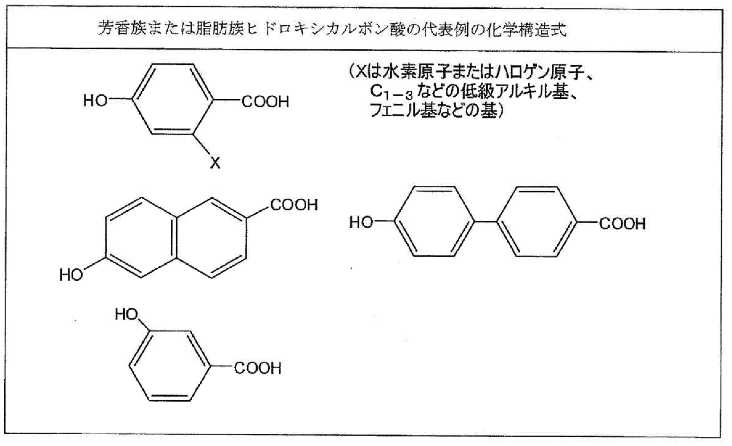
(4)芳香族ジアミン、芳香族ヒドロキシアミンまたは芳香族アミノカルボン酸(代表例は表4参照)

これらの原料化合物から得られる液晶ポリマーの代表例として表5および6に示す構造単位を有する共重合体を挙げることができる。
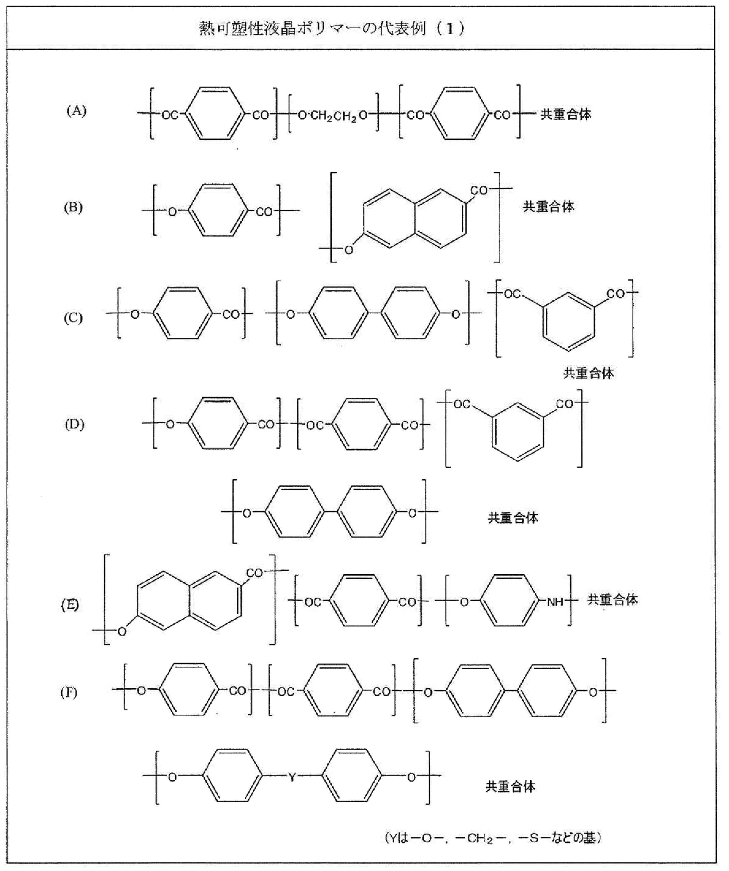
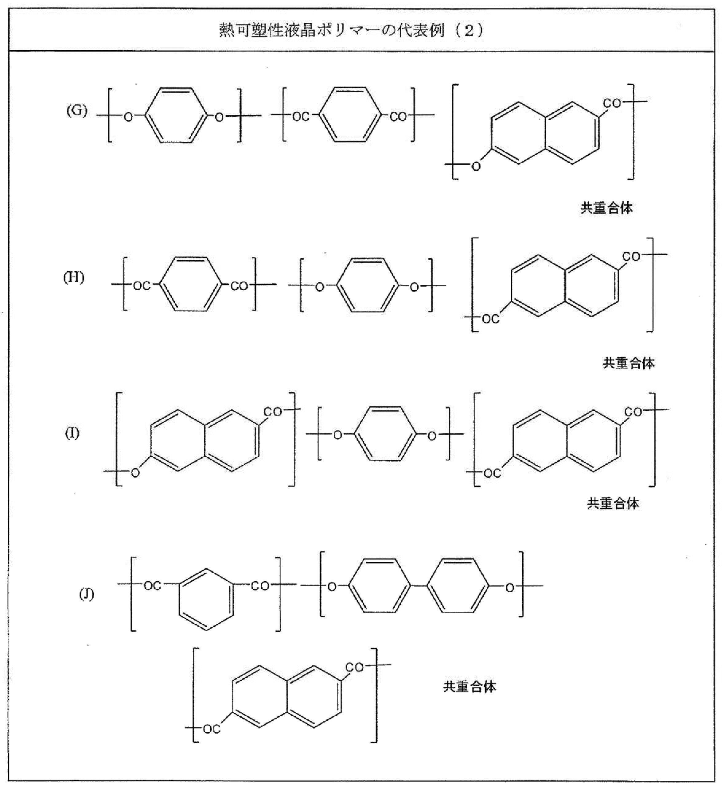
これらの共重合体のうち、p―ヒドロキシ安息香酸および/または6-ヒドロキシ-2-ナフトエ酸を少なくとも繰り返し単位として含む重合体が好ましく、特に、(i)p-ヒドロキシ安息香酸と6-ヒドロキシ-2-ナフトエ酸との繰り返し単位を含む重合体、(ii)p-ヒドロキシ安息香酸および6-ヒドロキシ-2-ナフトエ酸からなる群から選ばれる少なくとも一種の芳香族ヒドロキシカルボン酸と、4,4’-ジヒドロキシビフェニルおよびヒドロキノンからなる群から選ばれる少なくとも一種の芳香族ジオールと、テレフタル酸、イソフタル酸および2,6-ナフタレンジカルボン酸からなる群から選ばれる少なくとも一種の芳香族ジカルボン酸との繰り返し単位を含む重合体が好ましい。
例えば、(i)の重合体では、熱可塑性液晶ポリマーが、少なくともp-ヒドロキシ安息香酸と6-ヒドロキシ-2-ナフトエ酸との繰り返し単位を含む場合、繰り返し単位(A)のp-ヒドロキシ安息香酸と、繰り返し単位(B)の6-ヒドロキシ-2-ナフトエ酸とのモル比(A)/(B)は、液晶ポリマー中、(A)/(B)=10/90~90/10程度であるのが好ましく、より好ましくは、(A)/(B)=50/50~85/15程度であってもよく、さらに好ましくは、(A)/(B)=60/40~80/20程度であってもよい。
また、(ii)の重合体の場合、p-ヒドロキシ安息香酸および6-ヒドロキシ-2-ナフトエ酸からなる群から選ばれる少なくとも一種の芳香族ヒドロキシカルボン酸(C)と、4,4’-ジヒドロキシビフェニルおよびヒドロキノンからなる群から選ばれる少なくとも一種の芳香族ジオール(D)と、テレフタル酸、イソフタル酸および2,6-ナタレンジカルボン酸からなる群から選ばれる少なくとも一種の芳香族ジカルボン酸(E)の、液晶ポリマーにおける各繰り返し単位のモル比は、芳香族ヒドロキシカルボン酸(C):前記芳香族ジオール(D):前記芳香族ジカルボン酸(E)=30~80:35~10:35~10程度であってもよく、より好ましくは、(C):(D):(E)=35~75:32.5~12.5:32.5~12.5程度であってもよく、さらに好ましくは、(C):(D):(E)=40~70:30~15:30~15程度であってもよい。
また、芳香族ジカルボン酸に由来する繰り返し構造単位と芳香族ジオールに由来する繰り返し構造単位とのモル比は、(D)/(E)=95/100~100/95であることが好ましい。この範囲をはずれると、重合度が上がらず機械強度が低下する傾向がある。
なお、本発明にいう光学的異方性の溶融層(溶融時における光学的異方性)とは、例えば試料をホットステージにのせ、窒素雰囲気下で昇温加熱し、試料の透過光を観察することにより認定できる。
熱可塑性液晶ポリマーとして好ましいものは、融点(以下、Tm0と称す)が260~360℃の範囲のものであり、さらに好ましくはTm0が270~350℃のものである。なお、Tm0は示差走査熱量計((株)島津製作所DSC)により主吸熱ピークが現れる温度を測定することにより求められる。
熱可塑性液晶ポリマーには、本発明の効果を損なわない範囲内で、ポリエチレンテレフタレート、変性ポリエチレンテレフタレート、ポリオレフィン、ポリカーボネート、ポリアリレート、ポリアミド、ポリフェニレンサルファイド、ポリエーテルエーテルケトン、フッ素樹脂等の熱可塑性ポリマー、各種添加剤を添加してもよく、必要に応じて充填剤を添加してもよい。
本発明に使用される熱可塑性液晶ポリマーフィルムは、熱可塑性液晶ポリマーを押出成形して得られる。熱可塑性液晶ポリマーの剛直な棒状分子の方向を制御できる限り、任意の押出成形法が適用できるが、周知のTダイ法、ラミネート体延伸法、インフレーション法などが工業的に有利である。特にインフレーション法やラミネート体延伸法では、フィルムの機械加工方向(以下、MD方向と略す)だけでなく、これと直交する方向(以下、TD方向と略す)にも応力が加えられ、MD方向とTD方向における誘電特性を制御したフィルムが得られる。
押出成形では、配向を制御するために、延伸処理を伴うのが好ましく、例えば、Tダイ法による押出成形では、Tダイから押出した溶融体シートを、フィルムのMD方向だけでなく、これとTD方向の双方に対して同時に延伸してもよいし、またはTダイから押出した溶融体シートを一旦MD方向に延伸し、ついでTD方向に延伸してもよい。
また、インフレーション法による押出成形では、リングダイから溶融押出された円筒状シートに対して、所定のドロー比(MD方向の延伸倍率に相当する)およびブロー比(TD方向の延伸倍率に相当する)で延伸してもよい。
このような押出成形の延伸倍率は、MD方向の延伸倍率(またはドロー比)として、例えば、1.0~10程度であってもよく、好ましくは1.2~7程度、さらに好ましくは1.3~7程度であってもよい。また、TD方向の延伸倍率(またはブロー比)として、例えば、1.5~20程度であってもよく、好ましくは2~15程度、さらに好ましくは2.5~14程度であってもよい。
MD方向とTD方向とのそれぞれの延伸倍率の比(TD方向/MD方向)は、例えば、2.6以下、好ましくは0.4~2.5程度であってもよい。
また、熱可塑性液晶ポリマーフィルムには、押出成形した後に、必要に応じて延伸を行ってもよい。延伸方法自体は公知であり、二軸延伸、一軸延伸のいずれを採用してもよいが、分子配向度を制御することがより容易であることから、二軸延伸が好ましい。また、延伸は、公知の一軸延伸機、同時二軸延伸機、逐次二軸延伸機などが使用できる。
また、必要に応じて、公知または慣用の熱処理を行い、熱可塑性液晶ポリマーフィルムの融点および/または熱膨張係数を調整してもよい。熱処理条件は目的に応じて適宜設定でき、例えば、液晶ポリマーの融点(Tm0)-10℃以上(例えば、Tm0-10~Tm0+30℃程度、好ましくはTm0~Tm0+20℃程度)で数時間加熱することにより、熱可塑性液晶ポリマーフィルムの融点(Tm)を上昇させてもよい。
このようにして得られた本発明の熱可塑性液晶ポリマーフィルムは、優れた誘電特性、低吸湿性などを有しているため、回路基板材料として好適に用いることができる。
また、熱可塑性液晶ポリマーフィルムは、その剛直な構造に由来して、一般に低せん断領域での溶融粘度が高く、例えば、300℃における熱可塑性液晶ポリマーフィルムの溶融粘度(せん断速度1,000秒-1)は、例えば、100Pa・s以上であってもよく、好ましくは200~100,000Pa・s程度(例えば150~100,000Pa・s程度)、より好ましくは200~10,000Pa・s程度であってもよい。なお、溶融粘度は、粘弾性レオメータ(例えば、TA Instrucment Japan製AR2000)を用い、昇温速度3℃/分、周波数1Hz、ひずみ0.1%、法線応力5Nの条件下で測定することができる。
熱可塑性液晶ポリマーフィルムの融点(Tm)は、フィルムの所望の耐熱性および加工性を得る目的において、200~400℃程度の範囲内で選択することができ、好ましくは250~360℃程度、より好ましくは260~340℃程度であってもよい。なお、フィルムの融点は、示差走査熱量計を用いて、フィルムの熱挙動を観察して得ることができる。すなわち供試フィルムを20℃/分の速度で昇温して完全に溶融させた後、溶融物を50℃/分の速度で50℃まで急冷し、再び20℃/分の速度で昇温した後に現れる吸熱ピークの位置を、フィルムの融点として記録すればよい。
本発明において使用される熱可塑性液晶ポリマーフィルムは、任意の厚みであってもよく、そして、5mm以下の板状またはシート状のものをも包含する。ただし、高周波伝送線路に使用する場合は、厚みが厚いほど伝送損失が小さくなるので、できるだけ厚みを厚くするのが好ましい。電気絶縁層として熱可塑性液晶ポリマーフィルムを用いる場合、そのフィルムの膜厚は、10~500μmの範囲内にあることが好ましく、15~200μmの範囲内がより好ましい。フィルムの厚さが薄過ぎる場合には、フィルムの剛性や強度が小さくなることから、フィルム膜厚10~200μmの範囲のフィルムを積層させて任意の厚みを得る方法を使用してもよい。
本発明においては、導体層と熱圧着する熱可塑性液晶ポリマーフィルムの、導体層と熱圧着した後の該フィルムのASTM D882に準拠した方法により測定される靱性が30MPa以上100MPa以下であることが重要であり、好ましくは35MPa以上100MPa以下、より好ましくは50MPa以上100MPa以下、さらに好ましくは60MPa以上100MPa以下、特に好ましくは70MPa以上90MPa以下であってもよい。導体層との熱圧着後の靱性がこの範囲にある熱可塑性液晶ポリマーフィルムを用いることで、導体層などの被着体と積層したときのピール強度を高めることができ、熱圧着後においても高いピール強度を維持することができる。
本発明の熱可塑性液晶ポリマーフィルムは、該フィルムを銅箔と重ね合わせ、真空熱プレス装置を用いて圧着温度(加熱板の温度)を該フィルムの融点Tm-35℃に設定し、4MPaの圧力下、10分間熱圧着した後においても、銅箔を剥離した後の該フィルムの靭性が30MPa以上100MPa以下である。特に、上記圧着条件において、圧着温度をTm-35℃以上Tm-10℃以下の範囲のいずれに設定した場合であっても、靭性が30MPa以上100MPa以下となる熱可塑性液晶ポリマーフィルムが好ましい。
また、靱性の高いフィルムほど導体層のアンカー効果を顕著に反映して高いピール強度を与えるため、靱性の高いフィルムと、表面粗度が大きくアンカー効果の高い導体層とを組み合わせて圧着することで、より高いピール強度を得ることができる。
一般に、導体層の表面粗度が高いほどアンカー効果は高くなるが、表面の凹凸が大きくなることによる表皮効果により伝送損失が大きくなる。伝送損失を大きくしない範囲(例えば導体層表面のISO4287-1997に準拠した方法による十点平均粗度(RzJIS)が3μm以下)で導体層表面粗度を高くすることで、良好な高周波特性を維持しながら高いピール強度を実現することができる。靱性が30MPa未満である熱可塑性液晶ポリマーフィルムでは、伝送損失を大きくしない範囲で表面粗度を高くした導体層と圧着した場合に大きなピール強度を得ることができず、導体層表面の凹凸形状の特定や、凹凸間の距離を特定の範囲に限定するなどの特殊な加工が必要となるため、工程が煩雑になり、製造条件が限定される。
熱可塑性液晶ポリマーフィルムのような樹脂フィルムと導体層のような被着体との積層体について、樹脂フィルムと被着体とを剥離する場合、剥離の機構には界面剥離と凝集破壊の2つの機構が考えられる。積層体のピール強度がある程度強い場合、剥離の機構は主に凝集破壊で起こる。凝集破壊の際に樹脂フィルムの靱性が強いと剥離の際に樹脂フィルムが破壊されにくくなることから被着体と樹脂フィルムのピール強度が強くなると考えられる。
熱可塑性液晶ポリマーフィルムの靱性を高める手段としては、特に限定されないが、例えば、熱処理によってフィルムの靱性を高めてもよい。例えば、熱処理の際の熱処理温度、熱処理時間、昇温速度などを制御することで、フィルムに付与する靱性を調整することができ、例えば特定の昇温速度条件において、熱処理温度を高くすると熱可塑性液晶ポリマーフィルムに付与される靱性も高くなり、また熱処理時間を長くすると熱可塑性液晶ポリマーフィルムに付与される靱性も高くなる傾向がある。
熱処理温度の条件としては特に限定されないが、例えば熱可塑性液晶ポリマーフィルムの融点(Tm)-30℃以上(例えば、Tm-20℃~Tm+10℃程度、好ましくはTm~Tm+10℃程度)であってもよい。
熱処理時間の条件としては特に限定されないが、例えば1時間~20時間程度(例えば、5時間~15時間程度、好ましくは6時間~10時間程度)であってもよい。
昇温速度の条件としては、熱可塑性液晶ポリマーフィルムの靱性を高める観点から、例えば1℃/分~6℃/分が好ましく、より好ましくは1℃/分~3℃/分であり、生産性を考慮すると2℃/分が特に好ましい。
例えば、6-ヒドロキシ-2-ナフトエ酸単位27モル%、p-ヒドロキシ安息香酸単位73モル%からなるサーモトロピック液晶ポリエステルを、単軸押出機を用いて280~300℃で加熱混練し、直径40mm、スリット間隔0.6mmのインフレーションダイより押出して製膜した、融点280℃、厚さ50μmの熱可塑性液晶ポリマーフィルムを、窒素雰囲気下オーブン中において、昇温速度2℃/min程度、熱処理温度280℃程度、熱処理時間6時間程度の熱処理を施すことで、靱性が80MPa程度の熱可塑性液晶ポリマーフィルムを得ることができ、昇温速度4℃/min程度、熱処理温度280℃程度、熱処理時間5時間程度の熱処理を施すことで、靱性が70MPa程度の熱可塑性液晶ポリマーフィルムを得ることができる。
例えば、上記のような熱処理などによって、熱可塑性液晶ポリマーフィルムの靱性を高めてもよく、熱可塑性液晶ポリマーフィルムの靱性を高く設定することで、該フィルムと導体層とを熱圧着した後でも、該熱可塑性液晶ポリマーフィルムの靱性を30MPa以上100MPa以下に維持することができ、熱圧着後においても良好なピール強度を維持することができる。
熱可塑性液晶ポリマーフィルムと導体層を熱圧着した際のピール強度をより高めるために、熱可塑性液晶ポリマーフィルムの、ASTM D882規格に準拠した方法により測定されるヤング率は2.0GPa以上4.0GPa以下であることが好ましく、さらに2.5GPa以上4GPa以下がより好ましく、さらに2.5GPa以上3.5GPa以下がより好ましい。
熱可塑性液晶ポリマーフィルムのヤング率を調整する手段としては、特に限定されないが、例えば熱処理によりヤング率を調節しても良い。
例えば、熱処理温度を高くすると熱可塑性液晶ポリマーフィルムに付与されるヤング率は低くなる傾向がある。例えば、6-ヒドロキシ-2-ナフトエ酸単位27モル%、p-ヒドロキシ安息香酸単位73モル%からなるサーモトロピック液晶ポリエステルを、単軸押出機を用いて280~300℃で加熱混練し、直径40mm、スリット間隔0.6mmのインフレーションダイより押出して製膜した、融点280℃、厚さ50μmの熱可塑性液晶ポリマーフィルムを窒素雰囲気下オーブン中において昇温速度2℃/min程度、熱処理温度280℃程度、熱処理時間6時間程度の熱処理を施すことで、靱性が80MPa程度、ヤング率が3.5GPa程度の熱可塑性液晶ポリマーフィルムを得ることができる。
また、熱処理温度を低くするとヤング率は高くなる傾向があり、例えば、6-ヒドロキシ-2-ナフトエ酸単位27モル%、p-ヒドロキシ安息香酸単位73モル%からなるサーモトロピック液晶ポリエステルを、単軸押出機を用いて280~300℃で加熱混練し、直径40mm、スリット間隔0.6mmのインフレーションダイより押出して製膜した、融点280℃、厚さ50μmの熱可塑性液晶ポリマーフィルムを窒素雰囲気下オーブン中において昇温速度2℃/min程度、熱処理温度260℃程度、熱処理時間10時間程度の熱処理を施した場合、靱性が80MPa程度、ヤング率が5.0GPa程度の熱可塑性液晶ポリマーフィルムとなる。
熱可塑性液晶ポリマーフィルムに施す熱処理の温度が高いほどフィルムの靱性は高くなり、また熱処理時間が長いほどフィルムの靱性は高くなる傾向にある。このため、熱可塑性液晶ポリマーフィルムに特定の靱性を付与する際には、熱処理温度を高くして、熱処理時間を短く設定してもよいし、熱処理温度を低くして、熱処理時間を長く設定してもよい。熱可塑性液晶ポリマーフィルムのヤング率は例えば熱処理時間に影響を受ける傾向があり、熱処理時間が長いとヤング率が高くなる場合があるので、熱可塑性液晶ポリマーフィルムの靱性とヤング率との兼ね合いで熱処理温度および熱処理時間を調整し、靱性とヤング率を特定の範囲に設定することができる。例えばヤング率が特定の範囲になるような熱処理時間条件に応じて、熱処理温度を適宜設定することで、熱可塑性液晶ポリマーフィルムに特定の範囲の靱性とヤング率を付与することができる。
熱可塑性液晶ポリマーフィルムの靱性が30MPa以上100MPa以下の範囲であって、熱可塑性液晶ポリマーフィルムのヤング率が2.0GPa以上4.0GPa以下の範囲の場合、フィルムの靱性が高く、また、ヤング率が低いほど、導体層などの被着体と圧着した際のピール強度はより高くなる傾向がある。熱可塑性液晶ポリマーフィルムの熱処理などによってフィルムの靱性およびヤング率を調整する際には、靱性が高く、またヤング率が低くなるように調整すると、ピール強度をより高める観点から、より好ましい。
[導体層]
導体層は、少なくとも導電性を有する金属から形成され、この導体層に公知の回路加工方法を用いて回路が形成される。熱可塑性液晶ポリマーフィルムからなる絶縁性基材上に導体層を形成する方法としては、公知の方法を用いることができ、例えば、金属層を蒸着してもよく、無電解めっき、電解めっきにより、金属層を形成してもよい。また、金属箔(例えば銅箔)を熱圧着により、熱可塑性液晶ポリマーフィルムの表面に圧着してもよい。
導体層は、少なくとも導電性を有する金属から形成され、この導体層に公知の回路加工方法を用いて回路が形成される。熱可塑性液晶ポリマーフィルムからなる絶縁性基材上に導体層を形成する方法としては、公知の方法を用いることができ、例えば、金属層を蒸着してもよく、無電解めっき、電解めっきにより、金属層を形成してもよい。また、金属箔(例えば銅箔)を熱圧着により、熱可塑性液晶ポリマーフィルムの表面に圧着してもよい。
導体層を構成する金属箔は、電気的接続に使用されるような金属箔が好適であり、銅箔、のほか金、銀、ニッケル、アルミニウムなどの各種金属箔を挙げることができ、また実質的に(例えば、98質量%以上)これらの金属で構成される合金箔を含んでいてもよい。
これらの金属箔のうち、銅箔が好ましく用いられる。銅箔は、回路基板において用い得る銅箔であれば、特に限定されず、圧延銅箔、電解銅箔のいずれであってもよい。
また、導体層は、導体層の表面に耐酸化性の皮膜を形成していてもよい。例えば、その場合、ユニット回路基板の準備工程が、熱可塑性液晶ポリマーフィルムの片面または両面に金属箔を熱圧着する熱圧着工程と、熱圧着された金属箔表面に、耐酸化性皮膜を形成する耐酸化性皮膜形成工程とを備えていてもよい。
また、ユニット回路基板の準備工程は、導体層表面に、シランカップリング剤を付着するシランカップリング剤付着工程をさらに備えていてもよい。
耐酸化性皮膜としては、例えば、耐酸化性合金層、耐酸化性メッキ層、ベンゾトリアゾール類などの防錆剤層などが挙げられる。
なお、耐酸化性皮膜は、導体層および耐酸化性皮膜の種類に応じて、回路加工前、回路加工後のいずれに形成してもよい。
例えば、導体層が熱圧着された金属箔を含む場合、耐酸化性合金層としては、例えば、接着性を高める観点から、金属箔を形成する金属を少なくとも含む合金であるのが好ましい。例えば、導体層を構成する金属箔が銅箔の場合、合金層は少なくとも銅を含む合金であってもよい。例えば、耐酸化性合金層は、回路加工前に形成されるのが好ましい。
例えば、このような合金層は、メック(株)から上市されている「FlatBOND GT」などで形成してもよい。
なお、銅箔から離れる部分には、銅を含まない合金部分が存在する場合がある。その場合、銅を含まない合金部分については、エッチング液によりエッチングしてもよい。そのようなエッチング液としては、例えば「メックリムーバーS-651A」(メック(株)製)、「エスパック H-150」(佐々木化学薬品(株)製)、硝酸等の無機酸を含む水溶液などが挙げられる。
導体層の凹凸による表皮効果の影響を少なくし、低伝送損失を維持するには、導体層の表面粗度が小さいことが望ましい。導体層の表面粗度は、ISO4287-1997に準拠した方法による十点平均粗度(RzJIS)として、3μm以下であることが好ましく、より好ましくは2.0μm以下、更に好ましくは1.5μm以下であってもよい。十点平均粗度(RzJIS)の下限は特に限定されないが、例えば、0.1μm以上であってもよく、0.3μm以上であってもよく、0.5μm以上であってもよい。
上記構成の本発明において、積層体を形成する際に、ボンディングシートが被着されない面の導体層も平滑であってもよい。なお、導体層には回路が加工されるが、回路加工後に残る導体の表面が平滑であってもよい。
導体層の厚さは、例えば、1~50μmの範囲内が好ましく、5~20μmの範囲内がより好ましい。
さらに、導体層の接着性を向上させる観点から、導体層(特に合金層)表面に対して、公知または慣用のシランカップリング剤を付着させてもよい。
[回路基板]
回路基板(好ましくは多層回路基板)は、導体層が片面または両面に形成された熱可塑性液晶ポリマーフィルムからなる一以上のユニット回路基板と、このユニット回路基板の導体層に対して接着するための熱可塑性液晶ポリマーフィルムからなる一以上の回路基板材料とを有する回路基板であってもよく、回路基板材料と接着する側における導体層表面のISO4287-1997に準拠した方法による十点平均粗度(RzJIS)が3μm以下であってもよい。
[回路基板]
回路基板(好ましくは多層回路基板)は、導体層が片面または両面に形成された熱可塑性液晶ポリマーフィルムからなる一以上のユニット回路基板と、このユニット回路基板の導体層に対して接着するための熱可塑性液晶ポリマーフィルムからなる一以上の回路基板材料とを有する回路基板であってもよく、回路基板材料と接着する側における導体層表面のISO4287-1997に準拠した方法による十点平均粗度(RzJIS)が3μm以下であってもよい。
例えば、本発明の回路基板は、以下の構成を有する回路基板などであってもよい。
(i)熱可塑性の液晶ポリマーフィルムからなる絶縁層(基材層)と、フィルムの片面または両面上に形成された導体層とを有するユニット回路基板と、ボンディングシートとを備え、ボンディングシートを介してユニット回路基板が二枚以上積層した回路基板(多層回路基板)、
(ii)熱可塑性の液晶ポリマーフィルムからなる絶縁層(基材層)と、フィルムの片面または両面上に形成された導体層とを有するユニット回路基板と、このユニット回路基板の導体層をカバーするためのカバーレイとを備える回路基板(単層または二層回路基板)、
(iii)上記(i)および(ii)を組み合わせた構成であり、ユニット回路基板と、ボンディングシートと、カバーレイとを備え、二枚以上のユニット回路基板がボンディングシートを介して積層され、回路基板の最外層が、ユニット回路基板の導体層をカバーするカバーレイで構成されている回路基板(多層回路基板)、
(iv)熱可塑性の液晶ポリマーフィルムからなる絶縁層(基材層)を備えるユニット回路基板を複数枚備え、二枚以上のユニット回路基板が、ボンディングシートを介することなく直接積層した回路基板(多層回路基板)、および
(v)上記(ii)および(iv)を組み合わせた構成であり、二枚以上のユニット回路基板と、カバーレイとを備え、二枚以上のユニット回路基板がボンディングシートを介することなく直接積層され、回路基板の最外層が、ユニット回路基板の導体層をカバーするカバーレイで構成されている回路基板(多層回路基板)。
(i)熱可塑性の液晶ポリマーフィルムからなる絶縁層(基材層)と、フィルムの片面または両面上に形成された導体層とを有するユニット回路基板と、ボンディングシートとを備え、ボンディングシートを介してユニット回路基板が二枚以上積層した回路基板(多層回路基板)、
(ii)熱可塑性の液晶ポリマーフィルムからなる絶縁層(基材層)と、フィルムの片面または両面上に形成された導体層とを有するユニット回路基板と、このユニット回路基板の導体層をカバーするためのカバーレイとを備える回路基板(単層または二層回路基板)、
(iii)上記(i)および(ii)を組み合わせた構成であり、ユニット回路基板と、ボンディングシートと、カバーレイとを備え、二枚以上のユニット回路基板がボンディングシートを介して積層され、回路基板の最外層が、ユニット回路基板の導体層をカバーするカバーレイで構成されている回路基板(多層回路基板)、
(iv)熱可塑性の液晶ポリマーフィルムからなる絶縁層(基材層)を備えるユニット回路基板を複数枚備え、二枚以上のユニット回路基板が、ボンディングシートを介することなく直接積層した回路基板(多層回路基板)、および
(v)上記(ii)および(iv)を組み合わせた構成であり、二枚以上のユニット回路基板と、カバーレイとを備え、二枚以上のユニット回路基板がボンディングシートを介することなく直接積層され、回路基板の最外層が、ユニット回路基板の導体層をカバーするカバーレイで構成されている回路基板(多層回路基板)。
回路基板は、高い耐熱性を有する高融点液晶ポリマーフィルムと、それよりも低い耐熱性を有する低融点液晶ポリマーフィルムとで構成されていてもよく、例えば、絶縁基板、ボンディングシートおよびカバーレイから選択される少なくとも二種の回路基板材料が高い耐熱性を有する高融点液晶ポリマーフィルムと、それよりも低い耐熱性を有する低融点液晶ポリマーフィルムとで構成されていてもよい。この場合、高融点液晶ポリマーフィルムと、低融点液晶ポリマーフィルムとの融点差は、0~70℃程度であることが好ましく、0~60℃程度がより好ましい。
例えば、図1に示す例では、絶縁層である熱可塑性液晶ポリマーフィルム1の両面に導体層(銅箔)4が接合された第一のユニット回路基板10の上に、ボンディングシート3を介して、絶縁層である熱可塑性液晶ポリマーフィルム2の片面(上面)に導体層4が形成された第二のユニット回路基板20を積層した積層体(回路基板)30を例示しているが、図示された構成は、本発明の回路基板を限定するものではない。例えば、回路基板は、導体層を二枚のみ有するものであってもよく、四枚以上の導体層を有するものであってもよい。また、回路基板は、導体層をカバーするために、最外層に液晶ポリマーフィルムからなるカバーレイを備えていてもよい。
本発明の回路基板は、例えば、液晶ポリマーフィルムと導体層との間の接着強度(ピール強度)が0.6kN/m以上(例えば、0.6~2kN/m)であってもよく、好ましくは0.8kN/m以上であってもよく、さらに好ましくは1.0kN/m以上であってもよい。なお、この接着強度(ピール強度)は、JIS C5016-1994に準拠した方法により、毎分50mmの速度で、液晶ポリマーフィルムからなる接着性材料を、該液晶ポリマーフィルムと導体層との積層体に対して90°の方向に引きはがしながら、引っ張り試験機[日本電産シンポ(株)製、デジタルフォースゲージFGP-2]に準拠した方法により測定された引きはがし強さの値であってもよい。
本発明の回路基板は、誘電特性に優れる熱可塑性液晶ポリマーを絶縁材料として用いているため、特に高周波回路基板として好適に用いることができる。高周波回路は、単に高周波信号のみを伝送する回路からなるものだけでなく、高周波信号を低周波信号に変換して、生成された低周波信号を外部へ出力する伝送路や、高周波対応部品の駆動のために供給される電源を供給するための伝送路等、高周波信号ではない信号を伝送する伝送路も同一平面上に併設された回路も含まれる。
例えば、10GHzの周波数において、回路基板の比誘電率(εr)は、例えば2.6~3.5であってもよく、より好ましくは2.6~3.4であってもよい。
また、例えば、10GHzの周波数において、回路基板の誘電正接(Tanδ)は、例えば0.001から0.01であってもよく、より好ましくは0.001から0.008であってもよい。
[回路基板の製造方法]
以下、本発明にかかる回路基板の製造方法を説明する。
以下、本発明にかかる回路基板の製造方法を説明する。
(ユニット回路基板の準備)
まず、熱可塑性液晶ポリマーフィルムからなる絶縁性基材層と、この基材層の片面または両面に導体層が形成されたユニット回路基板を一枚以上準備する。熱可塑性液晶ポリマーフィルムおよび導体層については、上記に説明した構成のものを用いることができる。
まず、熱可塑性液晶ポリマーフィルムからなる絶縁性基材層と、この基材層の片面または両面に導体層が形成されたユニット回路基板を一枚以上準備する。熱可塑性液晶ポリマーフィルムおよび導体層については、上記に説明した構成のものを用いることができる。
(導体層に対して接着するための回路基板材料の準備)
導体層に対して接着するための回路基板材料(接着性材料)として、上記ユニット回路基板とは別に、ユニット回路基板の導体層と接着させるための回路基板材料を一以上準備してもよい。接着性材料は、熱可塑性液晶ポリマーフィルムであればよく、例えば、具体的には、ボンディングシートおよびカバーレイから選択される少なくとも一種が挙げられる。
導体層に対して接着するための回路基板材料(接着性材料)として、上記ユニット回路基板とは別に、ユニット回路基板の導体層と接着させるための回路基板材料を一以上準備してもよい。接着性材料は、熱可塑性液晶ポリマーフィルムであればよく、例えば、具体的には、ボンディングシートおよびカバーレイから選択される少なくとも一種が挙げられる。
なお、接着性材料として用いられる液晶ポリマーフィルムとしては、上述した熱可塑性液晶ポリマーフィルムに記載したものを用いることができる。回路基板の構成に応じて、接着性材料として用いられる液晶ポリマーフィルムの融点は、ユニット回路基板の基材の融点と同一であってもよいが、ユニット回路基板を形成する液晶ポリマーフィルムよりも、融点が低いものを用いるのが好ましい。その場合、両者の融点差は、例えば、0~70℃程度であってもよく、0~60℃程度がより好ましい。
(熱圧着工程)
熱可塑性液晶ポリマーフィルムと導体層とを熱圧着する手段としては特に限定されないが、例えば、バッチ式の真空熱プレス、ロールプレス、ダブルベルトプレスなどを用いることができる。ロールプレス、ダブルベルトプレスはロール・トゥ・ロールによるロールプレス、ダブルベルトプレスであってもよい。
熱可塑性液晶ポリマーフィルムと導体層とを熱圧着する手段としては特に限定されないが、例えば、バッチ式の真空熱プレス、ロールプレス、ダブルベルトプレスなどを用いることができる。ロールプレス、ダブルベルトプレスはロール・トゥ・ロールによるロールプレス、ダブルベルトプレスであってもよい。
バッチ式の真空熱プレスで熱可塑性液晶ポリマーフィルムと導体層(例えば金属箔)を積層する場合、例えば、真空熱プレス装置を使用して、その2枚の加熱板の間に所定の大きさに裁断された熱可塑性液晶ポリマーフィルムと金属箔を重ねて置き、真空状態で加熱圧着してもよい(バッチ式真空熱プレス積層法)。
ロールプレスによって、熱可塑性液晶ポリマーフィルムと導体層(例えば金属箔)を積層して積層体を形成し、片面金属張積層板を作製する場合、熱可塑性液晶ポリマーフィルムと金属箔を走行させ、合わせながら加熱された金属ロールとそれに接触したゴムロール間に導入し、ロール間を通過させて加熱圧着させ、積層体となすことで、フィルムの片面に金属箔が接合されてなる片面金属張積層板を作製してもよい。その際、ロール間通過前において、フィルムをゴムロールに沿わせ、次いで金属箔を該フィルムに合わせて仮接合させる予熱工程があってもよく、予熱工程は、フィルムがゴムロールと接触する角度が、ゴムロールと金属ロールの接点を基準にして90~120°の範囲となるように導入する予熱工程であってもよい。
ロールプレスによって、熱可塑性液晶ポリマーフィルムの両面に導体層(例えば金属箔)を積層して積層体を形成し、両面金属張積層板を作製する場合、熱可塑性液晶ポリマーフィルムの両面に金属箔が接合されてなる両面金属張積層板を加熱ロール間圧着により製造してもよい。その際、(1)2枚の金属箔が加熱ロールに接触する前にそれぞれ予熱される第1工程、(2)第1工程を経た2枚の100~250℃の温度に予熱された金属箔がそれぞれ1対をなす別個の加熱ロールに、1対の加熱ロールの接点を基準にして70~200°の角度θで接触して、加熱ロール上を搬送されながら、熱膨張して無緊張状態になる第2工程、および(3)第2工程により無緊張状態となり、1対をなす別個の加熱ロール上をそれぞれ搬送される2枚の金属箔とその間に搬送される熱可塑性液晶ポリマーフィルムとが、加熱ロール間で圧着されて一体化し、得られた積層板が加熱ロール間から搬送される第3工程を行うことを特徴とする両面金属張積層板の製造方法で製造してもよい。
ダブルベルトプレスによって、熱可塑性液晶ポリマーフィルムと導体層(例えば、金属箔)とを積層して積層体を形成する場合、まず、熱可塑性液晶ポリマーフィルムと金属箔とを重ね合わせ、次に、ダブルベルトプレスの中で熱可塑性液晶ポリマーフィルムの融点とフィルムの劣化点との間の温度において約5~500バールの圧力をかけて金属箔と該フィルムとをプレスし、接合させて積層体を形成してもよい。このとき、プレスの圧力は約5~100バールであってもよく、またプレス中でフィルムがその融点より高い温度にある滞在時間を0.5~1000秒としてもよく、また温度は、剥離強度が直線1cm当たり10N以上であり且つ寸度安定性は変化が±0.2%より小さい熱可塑性液晶ポリマー/金属箔積層体が得られるような温度であってもよい。
熱可塑性液晶ポリマーフィルムと導体層を熱圧着する際の、熱圧着温度はフィルムの融点Tm-30℃以下が好ましく、より好ましくはTm-35℃以下であってもよく、さらに好ましくはTm-40℃以下であってもよい。この温度範囲で熱圧着を行うことによって、熱圧着後の熱可塑性液晶ポリマーフィルムの靱性低下率をより抑えることができる。
熱可塑性液晶ポリマーフィルムと導体層とを熱圧着した後の液晶ポリマーフィルムの靱性の低下率は30%以内が好ましく、25%以内がより好ましく、15%以内がより好ましく、5%以内がさらに好ましい。熱圧着後の液晶ポリマーフィルムの靱性の低下率がこの範囲内であるとき、熱圧着後もより高いピール強度を維持することができる。
また、導体層と熱圧着する熱可塑性液晶ポリマーフィルムの、導体層と熱圧着した後の該フィルムの靱性が30MPa以上100MPa以下である限りにおいて、熱圧着時に加える圧力は、熱可塑性液晶ポリマーフィルムの性質に応じて、例えば、0.5~6MPaの広い範囲から選択することができる。例えば、プレス圧力が5MPa以下、特に4.5MPa以下(例えば、0.5MPa~3MPa、好ましくは、1~2.5MPa)であっても、液晶ポリマーフィルムと導体層間での良好な接着が可能である。
本発明の回路基板においては、熱可塑性液晶ポリマーフィルムと導体層との間の、JIS C5016-1994に準拠して測定した接着強度(ピール強度)が0.6kN/m以上が好ましく、0.8kN/m以上がより好ましく、1.0kN/m以上がさらに好ましい。
なお、本発明の効果を阻害しない範囲において、回路基板材料に対して表面処理を施してもよい。表面処理は、例えば、紫外線照射、プラズマ照射、物理的研磨などの公知の方法によって行うことができる。
以下、実施例により本発明をより詳細に説明するが、本発明は本実施例により何ら限定されるものではない。なお、以下の実施例及び比較例においては、下記の方法により各種物性を測定した。
(靱性(MPa))
熱可塑性液晶ポリマーフィルムの靱性(MPa)は、ASTM D882に準拠した方法により測定した伸度と最大引張強度の測定値から、下記式(1)により計算で求めた。
靱性=伸度×最大引張強度×1/2 (1)
熱可塑性液晶ポリマーフィルムの靱性(MPa)は、ASTM D882に準拠した方法により測定した伸度と最大引張強度の測定値から、下記式(1)により計算で求めた。
靱性=伸度×最大引張強度×1/2 (1)
また、熱圧着後の熱可塑性液晶ポリマーフィルムの靱性(MPa)は、熱可塑性液晶ポリマーフィルムと導体層を熱圧着した後、熱可塑性液晶ポリマーフィルムを導体層から剥離し、同様の方法で靱性(MPa)を求めた。
(熱圧着後の靱性低下率(%))
熱圧着前の熱可塑性液晶ポリマーフィルムの靱性(MPa)と、被着体と熱圧着後の該フィルムの靱性(MPa)をそれぞれ測定し、熱圧着前後の靱性の低下率を求めた。
靱性の低下率(%)=100×(熱圧着前の靱性(MPa)-熱圧着後の靱性(MPa))/熱圧着前の靱性(MPa)
熱圧着前の熱可塑性液晶ポリマーフィルムの靱性(MPa)と、被着体と熱圧着後の該フィルムの靱性(MPa)をそれぞれ測定し、熱圧着前後の靱性の低下率を求めた。
靱性の低下率(%)=100×(熱圧着前の靱性(MPa)-熱圧着後の靱性(MPa))/熱圧着前の靱性(MPa)
(ヤング率(GPa))
熱可塑性液晶ポリマーフィルムのヤング率(GPa)は、ASTM D882に準拠した方法により、フィルムに引張荷重を加え、その変位を求めることにより、下記式(2)より計算で求めた。
E=(σn+1-σn)/(εn+1-εn) (2)
(ここで、E:ヤング率(GPa)、σn+1-σn:引張荷重を変動させたときの引張応力の変化量、εn+1-εn:引張荷重を変動させたときの引張ひずみの変化量)
熱可塑性液晶ポリマーフィルムのヤング率(GPa)は、ASTM D882に準拠した方法により、フィルムに引張荷重を加え、その変位を求めることにより、下記式(2)より計算で求めた。
E=(σn+1-σn)/(εn+1-εn) (2)
(ここで、E:ヤング率(GPa)、σn+1-σn:引張荷重を変動させたときの引張応力の変化量、εn+1-εn:引張荷重を変動させたときの引張ひずみの変化量)
(表面粗度(RzJIS)(μm))
接触式表面粗さ計(ミツトヨ(株)製、型式 SJ-201)を用い、積層体で粗化処理された銅箔表面の十点平均粗さ(RzJIS)を測定した。測定はISO4287-1997に準拠した方法により行った。より詳細には、表面粗度(RzJIS)は、粗さ曲線からその平均線の方向に基準長さを抜き取り、最高から5番目までの山頂(凸の頂点)の標高の平均値と、最深から5番目までの谷底(凹の底点)の標高の平均値との差をμmで表わしたもので、十点平均粗さを示したものである。
接触式表面粗さ計(ミツトヨ(株)製、型式 SJ-201)を用い、積層体で粗化処理された銅箔表面の十点平均粗さ(RzJIS)を測定した。測定はISO4287-1997に準拠した方法により行った。より詳細には、表面粗度(RzJIS)は、粗さ曲線からその平均線の方向に基準長さを抜き取り、最高から5番目までの山頂(凸の頂点)の標高の平均値と、最深から5番目までの谷底(凹の底点)の標高の平均値との差をμmで表わしたもので、十点平均粗さを示したものである。
(接着強度:ピール強度(kN/m))
JIS C5016-1994に準拠した方法により、毎分50mmの速度で、液晶ポリマーフィルムからなる接着性材料を、液晶ポリマーフィルムと導体層との積層体に対して90°の方向に引きはがしながら、引っ張り試験機[日本電産シンポ(株)製、デジタルフォースゲージFGP-2]により、引きはがし強さを測定し、得られた値を接着強度(ピール強度)(kN/m)とした。
JIS C5016-1994に準拠した方法により、毎分50mmの速度で、液晶ポリマーフィルムからなる接着性材料を、液晶ポリマーフィルムと導体層との積層体に対して90°の方向に引きはがしながら、引っ張り試験機[日本電産シンポ(株)製、デジタルフォースゲージFGP-2]により、引きはがし強さを測定し、得られた値を接着強度(ピール強度)(kN/m)とした。
(伝送損失(db/cm)の測定)
マイクロ波ネットワークアナライザー[アジレント(Agilent)社製、型式:8722ES]とプローブ(カスケードマイクロテック社製、型式:ACP40-250)を用いて、マイクロストリップライン構造で測定周波数10GHzのS21パラメータを測定した。
マイクロ波ネットワークアナライザー[アジレント(Agilent)社製、型式:8722ES]とプローブ(カスケードマイクロテック社製、型式:ACP40-250)を用いて、マイクロストリップライン構造で測定周波数10GHzのS21パラメータを測定した。
[実施例1]
融点335℃、靱性80MPa、ヤング率3.5GPaの熱可塑性液晶ポリマーフィルムを準備した。この熱可塑性液晶ポリマーフィルムに対して導体層として表面粗度RzJISが2.5μmの圧延銅箔(三井金属(株)製、SQ-VLP、厚さ12μm)を重ね合わせ、真空熱プレス装置を用いて、加熱盤を300℃(熱可塑性液晶ポリマーフィルムの融点Tm-35℃)に設定し、4MPaの圧力下、10分間、熱圧着し積層体を作製した。
融点335℃、靱性80MPa、ヤング率3.5GPaの熱可塑性液晶ポリマーフィルムを準備した。この熱可塑性液晶ポリマーフィルムに対して導体層として表面粗度RzJISが2.5μmの圧延銅箔(三井金属(株)製、SQ-VLP、厚さ12μm)を重ね合わせ、真空熱プレス装置を用いて、加熱盤を300℃(熱可塑性液晶ポリマーフィルムの融点Tm-35℃)に設定し、4MPaの圧力下、10分間、熱圧着し積層体を作製した。
作製した積層体において、銅箔と熱可塑性液晶ポリマーフィルムとのピール強度および熱圧着後の熱可塑性液晶ポリマーフィルムの靱性を測定した。熱圧着後の熱可塑性液晶ポリマーフィルムの靱性低下はなかった。結果を表7に示す。
[実施例2]
融点325℃、靱性68MPa、ヤング率3.0GPaの熱可塑性液晶ポリマーフィルムを準備した。この熱可塑性液晶ポリマーフィルムに対して導体層として表面粗度RzJISが2.5μmの圧延銅箔(三井金属(株)製、SQ-VLP、厚さ12μm)を重ね合わせ、真空熱プレス装置を用いて、加熱盤を295℃(熱可塑性液晶ポリマーフィルムの融点Tm-30℃)に設定し、4MPaの圧力下、10分間、熱圧着し積層体を作製した。
融点325℃、靱性68MPa、ヤング率3.0GPaの熱可塑性液晶ポリマーフィルムを準備した。この熱可塑性液晶ポリマーフィルムに対して導体層として表面粗度RzJISが2.5μmの圧延銅箔(三井金属(株)製、SQ-VLP、厚さ12μm)を重ね合わせ、真空熱プレス装置を用いて、加熱盤を295℃(熱可塑性液晶ポリマーフィルムの融点Tm-30℃)に設定し、4MPaの圧力下、10分間、熱圧着し積層体を作製した。
作製した積層体において、銅箔と熱可塑性液晶ポリマーフィルムとのピール強度および熱圧着後の熱可塑性液晶ポリマーフィルムの靱性を測定した。熱圧着後の熱可塑性液晶ポリマーフィルムの靱性低下率は19%であった。結果を表7に示す。
[実施例3]
融点280℃、靱性42MPa、ヤング率2.5GPaの熱可塑性液晶ポリマーフィルムを準備した。この熱可塑性液晶ポリマーフィルムに対して導体層として表面粗度RzJISが2.5μmの圧延銅箔(三井金属(株)製、SQ-VLP、厚さ12μm)を重ね合わせ、真空熱プレス装置を用いて、加熱盤を250℃(熱可塑性液晶ポリマーフィルムの融点Tm-30℃)に設定し、4MPaの圧力下、10分間、熱圧着し積層体を作製した。
融点280℃、靱性42MPa、ヤング率2.5GPaの熱可塑性液晶ポリマーフィルムを準備した。この熱可塑性液晶ポリマーフィルムに対して導体層として表面粗度RzJISが2.5μmの圧延銅箔(三井金属(株)製、SQ-VLP、厚さ12μm)を重ね合わせ、真空熱プレス装置を用いて、加熱盤を250℃(熱可塑性液晶ポリマーフィルムの融点Tm-30℃)に設定し、4MPaの圧力下、10分間、熱圧着し積層体を作製した。
作製した積層体において、銅箔と熱可塑性液晶ポリマーフィルムとのピール強度および熱圧着後の熱可塑性液晶ポリマーフィルムの靱性を測定した。熱圧着後の熱可塑性液晶ポリマーフィルムの靱性低下率は17%であった。結果を表7に示す。
[実施例4]
融点335℃、靱性80MPa、ヤング率3.5GPaの熱可塑性液晶ポリマーフィルムを準備した。この熱可塑性液晶ポリマーフィルムに対して導体層として表面粗度RzJISが1.0μmの圧延銅箔(JX日鉱日石金属(株)製、BHY-X、厚さ12μm)を重ね合わせ、真空熱プレス装置を用いて、加熱盤を300℃(熱可塑性液晶ポリマーフィルムの融点Tm-35℃)に設定し、4MPaの圧力下、10分間、熱圧着し積層体を作製した。
融点335℃、靱性80MPa、ヤング率3.5GPaの熱可塑性液晶ポリマーフィルムを準備した。この熱可塑性液晶ポリマーフィルムに対して導体層として表面粗度RzJISが1.0μmの圧延銅箔(JX日鉱日石金属(株)製、BHY-X、厚さ12μm)を重ね合わせ、真空熱プレス装置を用いて、加熱盤を300℃(熱可塑性液晶ポリマーフィルムの融点Tm-35℃)に設定し、4MPaの圧力下、10分間、熱圧着し積層体を作製した。
作製した積層体において、銅箔と熱可塑性液晶ポリマーフィルムとのピール強度および熱圧着後の熱可塑性液晶ポリマーフィルムの靱性を測定した。熱圧着後の熱可塑性液晶ポリマーフィルムの靱性低下はなかった。結果を表7に示す。
[実施例5]
融点335℃、靱性80MPa、ヤング率3.5GPaの熱可塑性液晶ポリマーフィルムを準備した。この熱可塑性液晶ポリマーフィルムに対して導体層として表面粗度RzJISが1.0μmの圧延銅箔(JX日鉱日石金属(株)製、BHY-X、厚さ12μm)を重ね合わせ、真空熱プレス装置を用いて、加熱盤を325℃(熱可塑性液晶ポリマーフィルムの融点Tm-10℃)に設定し、4MPaの圧力下、10分間、熱圧着し積層体を作製した。
融点335℃、靱性80MPa、ヤング率3.5GPaの熱可塑性液晶ポリマーフィルムを準備した。この熱可塑性液晶ポリマーフィルムに対して導体層として表面粗度RzJISが1.0μmの圧延銅箔(JX日鉱日石金属(株)製、BHY-X、厚さ12μm)を重ね合わせ、真空熱プレス装置を用いて、加熱盤を325℃(熱可塑性液晶ポリマーフィルムの融点Tm-10℃)に設定し、4MPaの圧力下、10分間、熱圧着し積層体を作製した。
作製した積層体において、銅箔と熱可塑性液晶ポリマーフィルムとのピール強度および熱圧着後の熱可塑性液晶ポリマーフィルムの靱性を測定した。熱圧着後の熱可塑性液晶ポリマーフィルムの靱性低下率は37.5%であった。結果を表7に示す。
[比較例1]
融点320℃、靱性16MPa、ヤング率4.0GPaの熱可塑性液晶ポリマーフィルムを準備した。この熱可塑性液晶ポリマーフィルムに対して導体層として表面粗度RzJISが2.5μmの圧延銅箔(三井金属(株)製、SQ-VLP、厚さ12μm)を重ね合わせ、真空熱プレス装置を用いて、加熱盤を290℃(熱可塑性液晶ポリマーフィルムの融点Tm-30℃)に設定し、4MPaの圧力下、10分間、熱圧着し積層体を作製した。
融点320℃、靱性16MPa、ヤング率4.0GPaの熱可塑性液晶ポリマーフィルムを準備した。この熱可塑性液晶ポリマーフィルムに対して導体層として表面粗度RzJISが2.5μmの圧延銅箔(三井金属(株)製、SQ-VLP、厚さ12μm)を重ね合わせ、真空熱プレス装置を用いて、加熱盤を290℃(熱可塑性液晶ポリマーフィルムの融点Tm-30℃)に設定し、4MPaの圧力下、10分間、熱圧着し積層体を作製した。
作製した積層体において、銅箔と熱可塑性液晶ポリマーフィルムとのピール強度および熱圧着後の熱可塑性液晶ポリマーフィルムの靱性を測定した。熱圧着後の熱可塑性液晶ポリマーフィルムの靱性低下はなかった。結果を表7に示す。
[比較例2]
6-ヒドロキシ-2-ナフトエ酸単位27モル%、p-ヒドロキシ安息香酸単位73モル%からなるサーモトロピック液晶ポリエステルを、単軸押出機を用いて280~300℃で加熱混練し、直径40mm、スリット間隔0.6mmのインフレーションダイより押出し、厚さ50μmのフィルムを得た。このフィルムの融点Tmは280℃であり、靱性は20MPaであった。
6-ヒドロキシ-2-ナフトエ酸単位27モル%、p-ヒドロキシ安息香酸単位73モル%からなるサーモトロピック液晶ポリエステルを、単軸押出機を用いて280~300℃で加熱混練し、直径40mm、スリット間隔0.6mmのインフレーションダイより押出し、厚さ50μmのフィルムを得た。このフィルムの融点Tmは280℃であり、靱性は20MPaであった。
この熱可塑性液晶ポリマーフィルムに対して導体層として表面粗度RzJISが2.5μmの圧延銅箔(三井金属(株)製、SQ-VLP、厚さ12μm)を重ね合わせ、真空熱プレス装置を用いて、加熱盤を250℃(熱可塑性液晶ポリマーフィルムの融点Tm-30℃)に設定し、4MPaの圧力下、10分間、熱圧着し積層体を作製した。
作製した積層体において、銅箔と熱可塑性液晶ポリマーフィルムとのピール強度および熱圧着後の熱可塑性液晶ポリマーフィルムの靱性を測定した。熱圧着後の熱可塑性液晶ポリマーフィルムの靱性低下はなかった。結果を表7に示す。
[比較例3]
6-ヒドロキシ-2-ナフトエ酸単位27モル%、p-ヒドロキシ安息香酸単位73モル%からなるサーモトロピック液晶ポリエステルを、単軸押出機を用いて280~300℃で加熱混練し、直径40mm、スリット間隔0.6mmのインフレーションダイより押出し、厚さ50μmのフィルムを得た。このフィルムの融点Tmは280℃であった。
6-ヒドロキシ-2-ナフトエ酸単位27モル%、p-ヒドロキシ安息香酸単位73モル%からなるサーモトロピック液晶ポリエステルを、単軸押出機を用いて280~300℃で加熱混練し、直径40mm、スリット間隔0.6mmのインフレーションダイより押出し、厚さ50μmのフィルムを得た。このフィルムの融点Tmは280℃であった。
得られたフィルムに対し熱処理を行った。熱処理中、温度の昇温は行わず、フィルム表面温度を260℃に固定して4時間熱処理し、その後285℃に固定して6時間熱処理し、2段階の温度条件で熱処理を行った。得られた熱可塑性液晶ポリマーフィルムの融点Tmは350℃であり、靱性は20MPaであった。
この熱可塑性液晶ポリマーフィルムに対して導体層として表面粗度RzJISが1.0μmの圧延銅箔(JX日鉱日石金属(株)製、BHY-X、厚さ12μm)を重ね合わせ、真空熱プレス装置を用いて、加熱盤を300℃(熱可塑性液晶ポリマーフィルムの融点Tm-50℃)に設定し、4MPaの圧力下、10分間、熱圧着し積層体を作製した。
作製した積層体において、銅箔と熱可塑性液晶ポリマーフィルムとのピール強度および熱圧着後の熱可塑性液晶ポリマーフィルムの靱性を測定した。熱圧着後の熱可塑性液晶ポリマーフィルムの靱性低下はなかった。結果を表7に示す。
[比較例4]
6-ヒドロキシ-2-ナフトエ酸単位27モル%、p-ヒドロキシ安息香酸単位73モル%からなるサーモトロピック液晶ポリエステルを、単軸押出機を用いて280~300℃で加熱混練し、直径40mm、スリット間隔0.6mmのインフレーションダイより押出し、厚さ50μmのフィルムを得た。このフィルムの融点Tm は280℃であった。
6-ヒドロキシ-2-ナフトエ酸単位27モル%、p-ヒドロキシ安息香酸単位73モル%からなるサーモトロピック液晶ポリエステルを、単軸押出機を用いて280~300℃で加熱混練し、直径40mm、スリット間隔0.6mmのインフレーションダイより押出し、厚さ50μmのフィルムを得た。このフィルムの融点Tm は280℃であった。
得られたフィルムに対し熱処理を行った。熱処理中、温度の昇温は行わず、フィルム表面温度を260℃に固定して4時間熱処理し、その後300℃に固定して6時間熱処理し、2段階の温度条件で熱処理を行った。得られた熱可塑性液晶ポリマーフィルムの融点Tmは335℃であり、靱性は18MPaであった。
この熱可塑性液晶ポリマーフィルムに対して導体層として表面粗度RzJISが1.0μmの圧延銅箔(JX日鉱日石金属(株)製、BHY-X、厚さ12μm)を重ね合わせ、真空熱プレス装置を用いて、加熱盤を305℃(熱可塑性液晶ポリマーフィルムの融点Tm-30℃)に設定し、4MPaの圧力下、10分間、熱圧着し積層体を作製した。
作製した積層体において、銅箔と熱可塑性液晶ポリマーフィルムとのピール強度および熱圧着後の熱可塑性液晶ポリマーフィルムの靱性を測定した。熱圧着後の熱可塑性液晶ポリマーフィルムの靱性低下はなかった。結果を表7に示す。
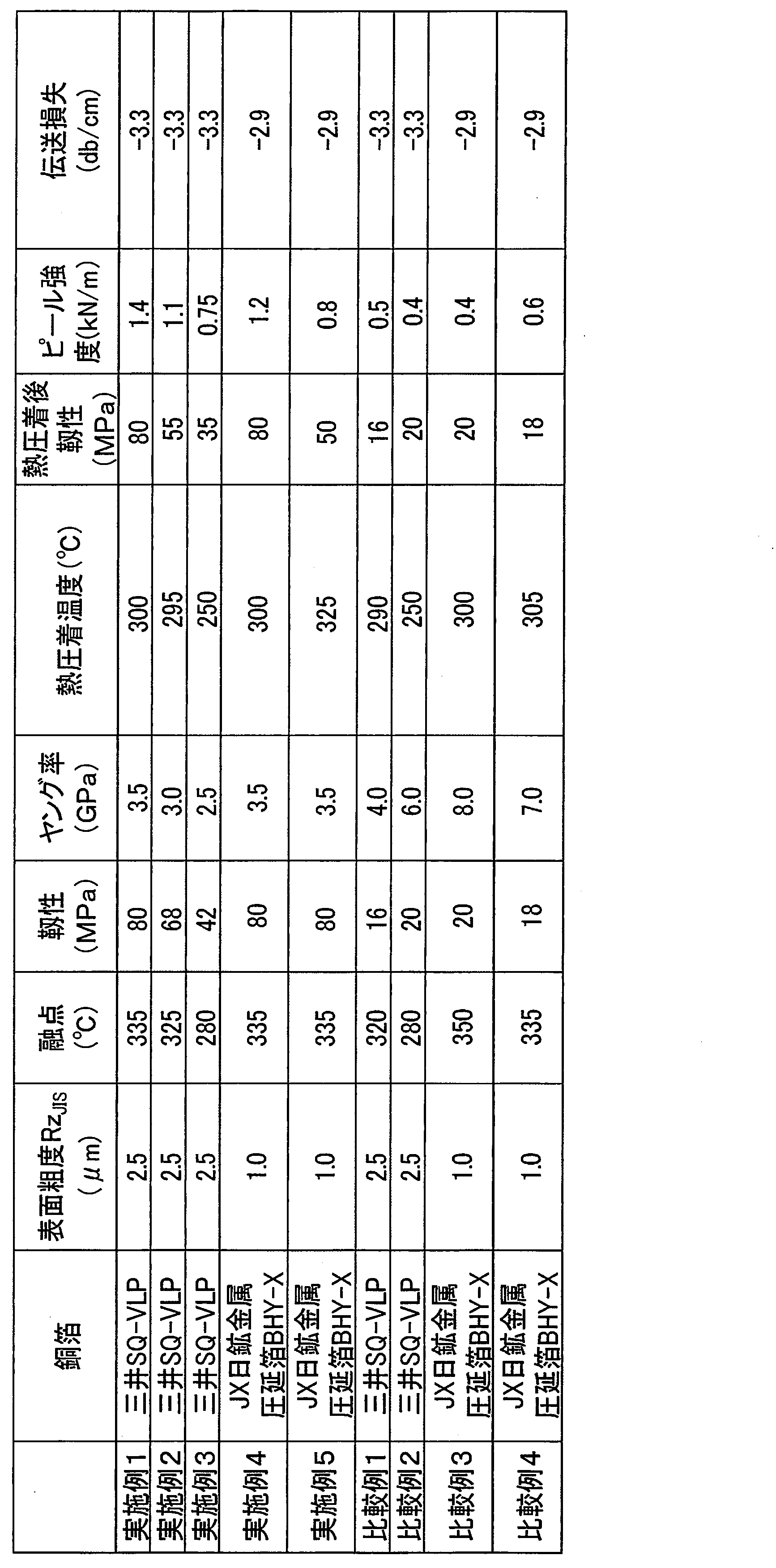
実施例1~3の結果から、熱圧着後の熱可塑性液晶ポリマーフィルムの靱性が高くなるほど、銅箔と熱可塑性液晶ポリマーフィルムとのピール強度が大きくなることがわかる。
比較例1~4の熱可塑性液晶ポリマーフィルムの靱性は30MPa未満であり、比較例1~4のような靱性が低いフィルムは、銅箔と該フィルムとのピール強度が0.6kN/m以下であり、低い値を示すことがわかる。
実施例4と実施例5を比較した場合、実施例4では熱可塑性液晶ポリマーフィルムと銅箔とを、熱可塑性液晶ポリマーフィルムの融点(Tm)-35℃の温度で圧着しているため、熱圧着後のフィルムの靱性は80MPaであり、熱圧着後の靱性の低下がないため、1.2kN/mの高いピール強度を与えていることがわかる。一方、実施例5では熱可塑性液晶ポリマーフィルムと銅箔とを、Tm-10℃の温度で圧着しているため、熱圧着後のフィルムの靱性は50MPaであり、その低下率は37.5%と大きく、結果、ピール強度は0.8kN/mであり、熱圧着後の靱性の低下率を低く抑えた実施例4の方が良好な結果が得られている。
また、表7に示すように、実施例1~5においては、比較例1~4と同等の伝送損失を得ることができており、以上より、実施例1~5においては、良好な高周波特性を維持しながら高いピール強度を実現できることがわかる。
1…熱可塑性液晶ポリマーフィルム
2…熱可塑性液晶ポリマーフィルム
3…ボンディングシート
4…導体層(銅箔)
10…第一のユニット回路基板
20…第二のユニット回路基板
30…積層体(回路基板)
2…熱可塑性液晶ポリマーフィルム
3…ボンディングシート
4…導体層(銅箔)
10…第一のユニット回路基板
20…第二のユニット回路基板
30…積層体(回路基板)
Claims (7)
- 熱可塑性液晶ポリマーフィルムであって、該熱可塑性液晶ポリマーフィルムを導体層と熱圧着した後の、該熱可塑性液晶ポリマーフィルムのASTM D882に準拠した方法により測定される靱性が30MPa以上100MPa以下である熱可塑性液晶ポリマーフィルム。
- 請求項1記載の熱可塑性液晶ポリマーフィルムであって、前記熱可塑性液晶ポリマーフィルムのASTM D882に準拠した方法により測定されるヤング率が2.0GPa以上4.0GPa以下である熱可塑性液晶ポリマーフィルム。
- 請求項1又は請求項2記載の熱可塑性液晶ポリマーフィルムであって、前記熱可塑性液晶ポリマーフィルムの融点Tm-30℃以下の温度において、該熱可塑性液晶ポリマーフィルムを導体層と熱圧着した後の、該熱可塑性液晶ポリマーフィルムの靱性低下率が30%以内である熱可塑性液晶ポリマーフィルム。
- 請求項1~請求項3のいずれか1項に記載の熱可塑性液晶ポリマーフィルムと、導体層とを積層してなる回路基板。
- 請求項4記載の回路基板において、前記導体層表面のISO4287-1997に準拠した方法により測定された十点平均粗度(RzJIS)が3μm以下である回路基板。
- 請求項4又は請求項5記載の回路基板において、前記熱可塑性液晶ポリマーフィルムと、該熱可塑性液晶ポリマーフィルムと接着した導体層との間におけるJIS C5016-1994に準拠した方法により測定された接着強度が0.6kN/m以上である回路基板。
- 熱可塑性液晶ポリマーフィルムと、該熱可塑性液晶ポリマーフィルムに積層された導体層とを含む回路基板であって、
前記導体層を前記熱可塑性液晶ポリマーフィルムから剥離した後の該熱可塑性液晶ポリマーフィルムのASTM D882に準拠した方法により測定される靱性が30MPa以上100MPa以下である回路基板。
Priority Applications (2)
| Application Number | Priority Date | Filing Date | Title |
|---|---|---|---|
| CN201680024465.8A CN107531921A (zh) | 2015-04-27 | 2016-04-26 | 热塑性液晶聚合物薄膜及电路板 |
| JP2017515392A JPWO2016174868A1 (ja) | 2015-04-27 | 2016-04-26 | 熱可塑性液晶ポリマーフィルム及び回路基板 |
Applications Claiming Priority (2)
| Application Number | Priority Date | Filing Date | Title |
|---|---|---|---|
| JP2015-090470 | 2015-04-27 | ||
| JP2015090470 | 2015-04-27 |
Publications (1)
| Publication Number | Publication Date |
|---|---|
| WO2016174868A1 true WO2016174868A1 (ja) | 2016-11-03 |
Family
ID=57198358
Family Applications (1)
| Application Number | Title | Priority Date | Filing Date |
|---|---|---|---|
| PCT/JP2016/002205 Ceased WO2016174868A1 (ja) | 2015-04-27 | 2016-04-26 | 熱可塑性液晶ポリマーフィルム及び回路基板 |
Country Status (4)
| Country | Link |
|---|---|
| JP (1) | JPWO2016174868A1 (ja) |
| CN (1) | CN107531921A (ja) |
| TW (2) | TW202126480A (ja) |
| WO (1) | WO2016174868A1 (ja) |
Cited By (13)
| Publication number | Priority date | Publication date | Assignee | Title |
|---|---|---|---|---|
| JP2021004365A (ja) * | 2018-11-08 | 2021-01-14 | 株式会社クラレ | 熱可塑性液晶ポリマーフィルムおよびそれを用いた回路基板 |
| US20210070927A1 (en) * | 2019-09-10 | 2021-03-11 | Ticona Llc | Polymer Composition and Film for Use in 5G Applications |
| JPWO2021177402A1 (ja) * | 2020-03-06 | 2021-09-10 | ||
| WO2021193385A1 (ja) * | 2020-03-26 | 2021-09-30 | 株式会社クラレ | 多層回路基板の製造方法 |
| US20230042016A1 (en) * | 2021-07-30 | 2023-02-09 | Fujifilm Corporation | Laminate |
| KR20230032878A (ko) | 2021-08-31 | 2023-03-07 | 후지필름 가부시키가이샤 | 액정 폴리머 필름, 적층체 |
| JP2023034584A (ja) * | 2021-08-31 | 2023-03-13 | 富士フイルム株式会社 | ポリマーフィルム、積層体 |
| JP2023034790A (ja) * | 2021-08-31 | 2023-03-13 | 富士フイルム株式会社 | ポリマーフィルム及び積層体 |
| US11840602B2 (en) | 2019-12-23 | 2023-12-12 | Chang Chun Plastics Co., Ltd. | Laminate, circuit board, and liquid crystal polymer film applied to the same |
| US11917753B2 (en) | 2019-09-23 | 2024-02-27 | Ticona Llc | Circuit board for use at 5G frequencies |
| JP2024059548A (ja) * | 2022-10-18 | 2024-05-01 | 佳勝科技股▲ふん▼有限公司 | 液晶ポリマーフィルムの製造方法 |
| US12103285B2 (en) | 2019-12-23 | 2024-10-01 | Chang Chun Plastics Co., Ltd. | Liquid crystal polymer film and laminate comprising the same |
| US20240368339A1 (en) * | 2023-05-05 | 2024-11-07 | Azotek Co., Ltd. | Laminate, multilayer board, and manufacturing method of laminate |
Families Citing this family (7)
| Publication number | Priority date | Publication date | Assignee | Title |
|---|---|---|---|---|
| TWI635952B (zh) * | 2017-05-10 | 2018-09-21 | 亞洲電材股份有限公司 | 複合式金屬基板結構 |
| WO2020090688A1 (ja) * | 2018-10-29 | 2020-05-07 | パナソニックIpマネジメント株式会社 | 金属張積層板、及び金属張積層板の製造方法 |
| CN112433405B (zh) * | 2020-11-24 | 2022-04-19 | 中国科学技术大学 | 一种液晶高分子基板及其加工方法 |
| CN112566364B (zh) * | 2020-11-24 | 2022-12-30 | 中国科学技术大学 | 无胶粘层热塑性液晶聚合物高频基板及其制备方法和应用 |
| WO2024043581A1 (ko) * | 2022-08-24 | 2024-02-29 | 코오롱인더스트리 주식회사 | 절연 필름 및 이를 포함하는 적층체 |
| TWI885448B (zh) * | 2023-05-05 | 2025-06-01 | 佳勝科技股份有限公司 | 積層板、多層板及製造積層板的方法 |
| CN117887120A (zh) * | 2023-12-29 | 2024-04-16 | 金发科技股份有限公司 | 一种液晶聚合物薄膜及其制备方法和应用 |
Citations (5)
| Publication number | Priority date | Publication date | Assignee | Title |
|---|---|---|---|---|
| JP2000044797A (ja) * | 1998-04-06 | 2000-02-15 | Kuraray Co Ltd | 液晶ポリマ―フィルムと積層体及びそれらの製造方法並びに多層実装回路基板 |
| WO2003102277A1 (en) * | 2002-06-04 | 2003-12-11 | Mitsui Mining & Smelting Co.,Ltd. | Surface treatment copper foil for low dielectric substrate, copper clad laminate including the same and printed wiring board |
| JP2005001376A (ja) * | 2003-05-21 | 2005-01-06 | Kuraray Co Ltd | フィルムの製造方法 |
| WO2007013330A1 (ja) * | 2005-07-27 | 2007-02-01 | Kuraray Co., Ltd. | 熱可塑性液晶ポリマーフィルムで被覆した配線板の製造方法 |
| JP2012077117A (ja) * | 2010-09-30 | 2012-04-19 | Kuraray Co Ltd | 熱可塑性液晶ポリマーフィルムおよびそれを用いた伝送線路 |
-
2016
- 2016-04-26 CN CN201680024465.8A patent/CN107531921A/zh active Pending
- 2016-04-26 WO PCT/JP2016/002205 patent/WO2016174868A1/ja not_active Ceased
- 2016-04-26 JP JP2017515392A patent/JPWO2016174868A1/ja active Pending
- 2016-04-27 TW TW110106897A patent/TW202126480A/zh unknown
- 2016-04-27 TW TW105113024A patent/TWI760302B/zh active
Patent Citations (5)
| Publication number | Priority date | Publication date | Assignee | Title |
|---|---|---|---|---|
| JP2000044797A (ja) * | 1998-04-06 | 2000-02-15 | Kuraray Co Ltd | 液晶ポリマ―フィルムと積層体及びそれらの製造方法並びに多層実装回路基板 |
| WO2003102277A1 (en) * | 2002-06-04 | 2003-12-11 | Mitsui Mining & Smelting Co.,Ltd. | Surface treatment copper foil for low dielectric substrate, copper clad laminate including the same and printed wiring board |
| JP2005001376A (ja) * | 2003-05-21 | 2005-01-06 | Kuraray Co Ltd | フィルムの製造方法 |
| WO2007013330A1 (ja) * | 2005-07-27 | 2007-02-01 | Kuraray Co., Ltd. | 熱可塑性液晶ポリマーフィルムで被覆した配線板の製造方法 |
| JP2012077117A (ja) * | 2010-09-30 | 2012-04-19 | Kuraray Co Ltd | 熱可塑性液晶ポリマーフィルムおよびそれを用いた伝送線路 |
Cited By (25)
| Publication number | Priority date | Publication date | Assignee | Title |
|---|---|---|---|---|
| JP7526622B2 (ja) | 2018-11-08 | 2024-08-01 | 株式会社クラレ | 熱可塑性液晶ポリマーフィルムの製造方法、熱可塑性液晶ポリマーフィルム、並びにそれを用いた金属張積層体および回路基板 |
| JP2021004365A (ja) * | 2018-11-08 | 2021-01-14 | 株式会社クラレ | 熱可塑性液晶ポリマーフィルムおよびそれを用いた回路基板 |
| US12209164B2 (en) * | 2019-09-10 | 2025-01-28 | Ticona Llc | Polymer composition and film for use in 5G applications |
| US20210070927A1 (en) * | 2019-09-10 | 2021-03-11 | Ticona Llc | Polymer Composition and Film for Use in 5G Applications |
| US11917753B2 (en) | 2019-09-23 | 2024-02-27 | Ticona Llc | Circuit board for use at 5G frequencies |
| US11945907B2 (en) | 2019-12-23 | 2024-04-02 | Chang Chun Plastics Co., Ltd. | Liquid crystal polymer film and laminate comprising the same |
| US11926698B2 (en) | 2019-12-23 | 2024-03-12 | Chang Chun Plastics Co., Ltd. | Liquid crystal polymer film and laminate comprising the same |
| US11840602B2 (en) | 2019-12-23 | 2023-12-12 | Chang Chun Plastics Co., Ltd. | Laminate, circuit board, and liquid crystal polymer film applied to the same |
| US12103285B2 (en) | 2019-12-23 | 2024-10-01 | Chang Chun Plastics Co., Ltd. | Liquid crystal polymer film and laminate comprising the same |
| JP7260054B2 (ja) | 2020-03-06 | 2023-04-18 | 株式会社村田製作所 | 液晶ポリマーフィルムおよびその製造方法 |
| WO2021177402A1 (ja) * | 2020-03-06 | 2021-09-10 | 株式会社村田製作所 | 液晶ポリマーフィルムおよびその製造方法 |
| JPWO2021177402A1 (ja) * | 2020-03-06 | 2021-09-10 | ||
| WO2021193385A1 (ja) * | 2020-03-26 | 2021-09-30 | 株式会社クラレ | 多層回路基板の製造方法 |
| US20230042016A1 (en) * | 2021-07-30 | 2023-02-09 | Fujifilm Corporation | Laminate |
| KR20230032878A (ko) | 2021-08-31 | 2023-03-07 | 후지필름 가부시키가이샤 | 액정 폴리머 필름, 적층체 |
| JP2023034673A (ja) * | 2021-08-31 | 2023-03-13 | 富士フイルム株式会社 | 液晶ポリマーフィルム、積層体 |
| JP2023034790A (ja) * | 2021-08-31 | 2023-03-13 | 富士フイルム株式会社 | ポリマーフィルム及び積層体 |
| JP2023034584A (ja) * | 2021-08-31 | 2023-03-13 | 富士フイルム株式会社 | ポリマーフィルム、積層体 |
| JP7702310B2 (ja) | 2021-08-31 | 2025-07-03 | 富士フイルム株式会社 | ポリマーフィルム、積層体 |
| JP7702311B2 (ja) | 2021-08-31 | 2025-07-03 | 富士フイルム株式会社 | 液晶ポリマーフィルム、積層体 |
| JP7703402B2 (ja) | 2021-08-31 | 2025-07-07 | 富士フイルム株式会社 | ポリマーフィルム及び積層体 |
| JP2024059548A (ja) * | 2022-10-18 | 2024-05-01 | 佳勝科技股▲ふん▼有限公司 | 液晶ポリマーフィルムの製造方法 |
| JP7731147B2 (ja) | 2022-10-18 | 2025-08-29 | 佳勝科技股▲ふん▼有限公司 | 液晶ポリマーフィルムの製造方法 |
| US12540221B2 (en) | 2022-10-18 | 2026-02-03 | Azotek Co., Ltd. | Method for manufacturing liquid crystal polymer film |
| US20240368339A1 (en) * | 2023-05-05 | 2024-11-07 | Azotek Co., Ltd. | Laminate, multilayer board, and manufacturing method of laminate |
Also Published As
| Publication number | Publication date |
|---|---|
| CN107531921A (zh) | 2018-01-02 |
| TW202126480A (zh) | 2021-07-16 |
| JPWO2016174868A1 (ja) | 2018-02-15 |
| TWI760302B (zh) | 2022-04-11 |
| TW201702067A (zh) | 2017-01-16 |
Similar Documents
| Publication | Publication Date | Title |
|---|---|---|
| TWI760302B (zh) | 電路基板 | |
| JP6656231B2 (ja) | 金属張積層板の製造方法およびこれを用いた金属張積層板 | |
| TWI616328B (zh) | 熱塑性液晶聚合物薄膜及使用其之積層體及電路基板、積層體之製造方法、以及熱塑性液晶聚合物薄膜之製造方法 | |
| JP6632541B2 (ja) | 回路基板およびその製造方法 | |
| JP6499584B2 (ja) | 熱可塑性液晶ポリマーフィルム、回路基板、およびそれらの製造方法 | |
| JP4216433B2 (ja) | 回路基板用金属張積層板の製造方法 | |
| CN102781661B (zh) | 单面金属包覆层叠体的制造方法 | |
| JP6019012B2 (ja) | 高周波回路基板 | |
| JP6031352B2 (ja) | 両面金属張積層体の製造方法 | |
| JP2019178326A (ja) | 熱可塑性液晶ポリマーフィルムの製造方法、並びに回路基板及びその製造方法 | |
| JP4866853B2 (ja) | 熱可塑性液晶ポリマーフィルムで被覆した配線基板の製造方法 | |
| JP5234647B2 (ja) | 複合接着フィルムおよびそれを用いた多層回路基板並びにその製造方法 | |
| JP2016107507A (ja) | 金属張積層板およびその製造方法 | |
| WO2021193385A1 (ja) | 多層回路基板の製造方法 | |
| JP6202905B2 (ja) | 回路基板およびその製造方法 | |
| JP2011216598A (ja) | 高周波回路基板 | |
| JP2007019338A (ja) | 電子回路基板およびその製造方法 | |
| TW202440747A (zh) | 熱塑性液晶聚合物薄膜及積層體、以及彼等之製造方法 | |
| WO2024219160A1 (ja) | フレキシブル金属張積層板、及びその製造方法 | |
| KR20220020270A (ko) | 금속 피복 적층체의 제조 방법 | |
| JP2025147696A (ja) | フレキシブル金属張積層板、及びその製造方法 |
Legal Events
| Date | Code | Title | Description |
|---|---|---|---|
| 121 | Ep: the epo has been informed by wipo that ep was designated in this application |
Ref document number: 16786145 Country of ref document: EP Kind code of ref document: A1 |
|
| ENP | Entry into the national phase |
Ref document number: 2017515392 Country of ref document: JP Kind code of ref document: A |
|
| NENP | Non-entry into the national phase |
Ref country code: DE |
|
| 122 | Ep: pct application non-entry in european phase |
Ref document number: 16786145 Country of ref document: EP Kind code of ref document: A1 |