WO2016171507A1 - 전자파 차폐 구조물 - Google Patents
전자파 차폐 구조물 Download PDFInfo
- Publication number
- WO2016171507A1 WO2016171507A1 PCT/KR2016/004216 KR2016004216W WO2016171507A1 WO 2016171507 A1 WO2016171507 A1 WO 2016171507A1 KR 2016004216 W KR2016004216 W KR 2016004216W WO 2016171507 A1 WO2016171507 A1 WO 2016171507A1
- Authority
- WO
- WIPO (PCT)
- Prior art keywords
- shielding structure
- surface roughness
- metal layer
- electromagnetic shielding
- electromagnetic
- Prior art date
- Legal status (The legal status is an assumption and is not a legal conclusion. Google has not performed a legal analysis and makes no representation as to the accuracy of the status listed.)
- Ceased
Links
Images



Classifications
-
- H—ELECTRICITY
- H05—ELECTRIC TECHNIQUES NOT OTHERWISE PROVIDED FOR
- H05K—PRINTED CIRCUITS; CASINGS OR CONSTRUCTIONAL DETAILS OF ELECTRIC APPARATUS; MANUFACTURE OF ASSEMBLAGES OF ELECTRICAL COMPONENTS
- H05K9/00—Screening of apparatus or components against electric or magnetic fields
- H05K9/0073—Shielding materials
- H05K9/0081—Electromagnetic shielding materials, e.g. EMI, RFI shielding
- H05K9/0088—Electromagnetic shielding materials, e.g. EMI, RFI shielding comprising a plurality of shielding layers; combining different shielding material structure
-
- H—ELECTRICITY
- H05—ELECTRIC TECHNIQUES NOT OTHERWISE PROVIDED FOR
- H05K—PRINTED CIRCUITS; CASINGS OR CONSTRUCTIONAL DETAILS OF ELECTRIC APPARATUS; MANUFACTURE OF ASSEMBLAGES OF ELECTRICAL COMPONENTS
- H05K9/00—Screening of apparatus or components against electric or magnetic fields
- H05K9/0007—Casings
- H05K9/002—Casings with localised screening
- H05K9/0022—Casings with localised screening of components mounted on printed circuit boards [PCB]
- H05K9/0024—Shield cases mounted on a PCB, e.g. cans or caps or conformal shields
- H05K9/0026—Shield cases mounted on a PCB, e.g. cans or caps or conformal shields integrally formed from metal sheet
Definitions
- Embodiments of the present invention are directed to a structure capable of effectively shielding electromagnetic waves of electronic components.
- electromagnetic magnetic interference is referred to as a metal member in a functionally classified unit device.
- EMI electromagnetic magnetic interference
- the present invention has been made to solve the above-mentioned problem, in particular, by implementing a functional layer for shielding the electric wave inside the electromagnetic shielding structure, to fundamentally block the electromagnetic leak (EMI leak), for various electronic devices
- EMI leak electromagnetic leak
- the electromagnetic shielding structure according to the present embodiment for solving the above problems is an electromagnetic wave generating source for generating electromagnetic waves; A shielding structure filling the electromagnetic wave generating source and including surface roughness on a surface thereof; And an electromagnetic shielding metal layer filling the shielding structure and forming a surface roughness corresponding to the surface roughness of the shielding structure, wherein the shielding structure has different surface roughnesses from the top and the side surfaces thereof.
- the surface roughness Ra of the side surface of the shielding structure may be formed more precisely than the surface roughness Ra of the upper surface.
- the surface roughness Ra of the upper surface of the shielding structure may be formed in the range of 1 ⁇ m to 30.0 ⁇ m.
- the surface roughness Ra of the side surface of the shielding structure may be formed in the range of 0.1 ⁇ m to 10.0 ⁇ m.
- the thickness of the electromagnetic shielding metal layer may be formed to 1 ⁇ m to 10 ⁇ m.
- the surface roughness of the electromagnetic shielding metal layer may be formed by patterning at least two or more metal layers inside the upper and side surfaces of the shielding structure.
- the metal layer may be formed of a laminated structure of a metal layer including Cu or Ni.
- the metal layer may be an electroless Cu plating layer, an electrolytic Cu plating layer and an electrolytic Ni plating layer.
- the present invention by implementing a functional layer for electric vehicle shielding inside the electromagnetic shielding structure, by blocking the electromagnetic leak (EMI leak) at the source, by efficiently implementing the electromagnetic shielding for various electronic devices In addition, it has the effect of minimizing performance degradation and malfunction of electronic components.
- EMI leak electromagnetic leak
- a blister phenomenon or side slipping phenomenon in which bubbles are generated on the surface of the component generated during the reliability test of the electronic component is prevented. It can be removed, and can maximize the blocking rate of the electromagnetic shielding structure to increase the reliability.
- FIG. 1 is a conceptual diagram of a package to which an electromagnetic shielding structure according to an embodiment of the present invention is applied
- FIG. 2 is an enlarged conceptual view of the electromagnetic shielding structure of FIG. 1.
- FIG. 3 is a flow chart showing a fixing for implementing the surface roughness of the shielding structure according to an embodiment of the present invention.
- FIG. 4 is a diagram illustrating a method of implementing surface roughness using a laser according to an embodiment of the present invention.
- 5 through 8 are cross-sectional views of the upper surface of the shielding structure of the embodiment of the present invention.
- 9 and 10 are cross-sectional views of side surfaces of shield structures of embodiments of the present invention.
- 11 is an experimental graph of shielding efficiency according to the thickness of the electromagnetic shielding metal layer in the embodiment of the present invention.
- FIG. 12 is an experimental graph illustrating electromagnetic shielding efficiency of a harmonic band of 1 GHz to 10 GHz in a shield structure having the same structure as that of FIG. 11.
- FIG. 1 is a conceptual diagram of a package to which an electromagnetic shielding structure according to an embodiment of the present invention is applied
- FIG. 2 is an enlarged conceptual view of the electromagnetic shielding structure of FIG. 1.
- an electromagnetic wave shielding structure according to an embodiment of the present invention includes an electromagnetic wave source 20 for generating electromagnetic waves, a shielding structure 100 for embedding the electromagnetic wave source 20, and the shielding structure 100. ) And a shielding metal layer (120) to bury it.
- the electromagnetic wave generator 20 is disposed on the printed circuit board 10, and an adjacent element 30 may be further disposed on the periphery of the electromagnetic wave generator 20.
- the shielding structure 100 has a surface roughness (roughness) is formed on the surface, more specifically, the shielding structure 100 is formed with a different surface roughness of the upper surface 101 and the side surface (102).
- the electromagnetic shielding metal layer 120 is a surface treatment is implemented through the physical or chemical processing on the inner surface of the shielding structure 100, between the surface of the shielding structure 100 and the electromagnetic shielding metal layer 120 It is possible to eliminate the mismatch of coefficient of thermal expansion (CTE) between materials and the adhesion failure caused by the difference in surface energy, and to provide sufficient anchoring energy. It is possible to eliminate blister and side shiping.
- CTE coefficient of thermal expansion
- a uniform film formation is formed on the side surface 102 so as to prevent the leakage phenomenon of electromagnetic waves generated from the side surface 102 of the shielding structure 100 to increase the shielding performance.
- the shielding structure 100 may be formed in a structure covering and covering an electronic component and an electronic device serving as various electromagnetic wave generating sources 20 as a whole.
- the electromagnetic wave generation source 20 is implemented in a structure that is mounted on the same substrate as the printed circuit board 10, the shielding structure 100 is formed in a structure in close contact with the printed circuit board 10 In this case, in particular, the electromagnetic shielding metal layer 120 is formed in the close contact portion of the shielding structure 100 and the printed circuit board 10 so as to block electromagnetic leakage.
- the shielding structure 100 may be implemented to be physical or chemical processing to have a constant surface roughness, the surface of the thin film through a process such as plating on the inner surface having such surface roughness
- the metal layer is formed to form an electromagnetic shielding metal layer 120.
- the surface roughness corresponding to the surface roughness of the shielding structure 100 is formed on the shielding metal layer 120.
- the surface roughness of the upper surface 101 of the shielding structure 100 and the surface roughness of the side surface 102 are different from each other in consideration of the influence of the electromagnetic waves from the electromagnetic wave source 20 formed in the shielding structure 100. can do.
- the size of the surface roughness Ra of the side surface 102 of the shielding structure 100 or the electromagnetic shielding metal layer 120 is smaller than the size of the surface roughness Ra of the upper surface 101.
- the size of the top surface roughness (Rb) may be 10 to 250 times the size of the side surface roughness (Ra).
- the surface roughness Ra of the upper surface 101 of the shielding structure 100 is in the range of 1 ⁇ m to 30.0 ⁇ m, and the surface roughness Ra of the side surface 102 of the shielding structure 100. May be implemented in the range of 0.1 ⁇ m to 10.0 ⁇ m.
- a defect in which a blister phenomenon or a chipping phenomenon, which is a local scratch at the interface, is significantly increased between the metal layer and the surface of the shielding structure 100, may be significantly increased.
- the surface roughness of the shielding structure 100 in the embodiment of the present invention after performing a surface treatment through the physical and chemical processing on the surface of the shielding structure 100, implements the metal layer 120 It can be implemented in such a way that the surface roughness is naturally transferred to the metal layer 120.
- the surface roughness may be realized by patterning the metal layer 120.
- FIG 3 is a flowchart illustrating a method of implementing the surface roughness of the shielding structure according to an embodiment of the present invention
- Figure 4 is a view showing a method of implementing the surface roughness using a laser according to an embodiment of the present invention.
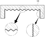
- FIGS. 5-8 are cross-sectional views of the top surface 101 of the shielding structure of an embodiment of the present invention
- FIGS. 9 and 10 are cross-sectional views of the side surfaces 102 of the shielding structure of an embodiment of the present invention.
- an area for implementing the surface roughness is formed by adhering a foamed tape to the surface of the inside of the shielding structure. (S310).
- a surface treatment operation for implementing surface roughness on the surface of the inside of the shielding structure is performed (S320).
- the surface treatment operation may be implemented using a physical surface treatment method after chemical surface treatment.
- Examples of chemical surface treatment methods include swelling using glycol ether, etching using an etchant such as KMnO 4 , neutralization using acidic liquids such as sulfuric acid, and the like. There is this.
- the surface roughness 103 may be formed by irradiating a laser on the surface of the shielding structure 110.
- the physical surface treatment may be applied to the method of implementing the surface roughness using E-Beam, UV laser, CO2 laser.
- it can be processed by setting the electron energy 30keV, E-Beam diameter 30 ⁇ m ⁇ 50 ⁇ m, the application time 10 ⁇ 20 minutes.
- the inner surface of the upper surface 101 of the shielding structure may have a roughness Ra in a range of 1 ⁇ m to 30.0 ⁇ m, and as shown in FIGS. 9 and 10.
- roughness Ra can be formed in the range of 0.1 micrometer-10.0 micrometers.
- the metal layer may be implemented through the first plating process (S330).
- the metal layer forms a first metal layer (such as a Cu metal layer) through electroless plating, and the Cu metal layer has a constant surface roughness as well as a high adhesion to the surface by the surface roughness of the surface of the shielding structure. It can be formed as.
- the metal layer may be implemented in a structure in which a metal layer of Cu and Ni is laminated by using an electroplating method on the first metal layer.
- the thickness of the electromagnetic shielding metal layer in the embodiment of the present invention is implemented in the range of 1 ⁇ m ⁇ 12 ⁇ m, efficiency of about 250% compared to the shielding rate when there is no metal shielding electromagnetic layer Augmentation can be implemented.
- the electromagnetic shielding metal layer in the embodiment of the present invention implemented as an electroless Cu plating layer 12 ⁇ m, the surface roughness of the upper surface 101 of the shielding structure 1 ⁇ m ⁇ 7.0 ⁇ m, the average range of 5 ⁇ m
- the surface roughness of the side surface 102 is implemented to have a range of 0.01 ⁇ m to 3.0 ⁇ m and an average of 2 ⁇ m, the shielding efficiency of the electromagnetic wave of the low frequency band in the range of 30 MHz to 1 GHz is tested.
- the Ag metal layer was formed to a thickness of 20 ⁇ m by a spray process, the Al tape was 350 ⁇ m thick, and Ag was SPT 6 ⁇ m thick.
- the shielding efficiency (approximately 4 dB, 250% improvement) is high in an example implemented with 12 ⁇ m of the electroless Cu plating layer of the present invention in the entire range of the frequency range.
- FIG. 12 is a graph illustrating electromagnetic shielding efficiency of a harmonic band of 1 GHz to 10 GHz in a shield structure having the same structure as that of FIG. 11 and comparing the shielding efficiency with a comparative example that does not implement a metal layer.
Landscapes
- Engineering & Computer Science (AREA)
- Microelectronics & Electronic Packaging (AREA)
- Physics & Mathematics (AREA)
- Electromagnetism (AREA)
- Shielding Devices Or Components To Electric Or Magnetic Fields (AREA)
- Laminated Bodies (AREA)
Abstract
실시예에 따르면, 전자파 발생원을 둘러싸며 표면에 표면 조도(roughness)를 포함하는 차폐 구조물; 및 상기 차폐 구조물의 표면에 배치되어 상기 차폐 구조물을 둘러싸는 전자파 차폐용 금속층을 포함하며, 상기 차폐 구조물 상면과 측면의 표면 조도는 서로 상이한 전자파 차폐 구조물이 제공된다.
Description
본 발명의 실시예는 전자부품의 전자파를 효율적으로 차폐할 수 있는 구조물에 대한 것이다.
최근 전자제품 내의 부품이 집적화되고 처리속도가 고속화됨에 따라, 각 부품별 성능을 극대화되고, 인접 부품과의 전자기적 간섭에 의한 오작동, 성능저하, 열화 현상이 발생하는 문제가 있다.
이와 같은 인접 전자부품간의 전자기적 간섭현상을 방지하고 성능 향상을 위하여 기능적으로 분류된 단위 부품(device)에 금속 부재 등으로 전자파로 인한 방해(EMI;electro magnetic interference, 이하, 'EMI'라 한다.) 차폐를 구현한다.
하지만, 금속 부재의 경우 대상이 되는 소자를 커버하기 위해 넓은 부위를 덮어야 하고, 인접소자 및 해당 성능과 무관한 소자까지 커버해야 하며, 금속 부재의 높이, 금속 부재의 재질의 두께 등도 전자부품별로 고려해야하는 문제가 된다. 또한, 완전한 EMI 차폐는 어려워 전자부품이 실장되는 인쇄회로기판의 표면과 상술한 금속부재가 체결된 부위에서 전자파누설(EMI leak) 현상이 많이 발생한다.
본 발명은 전술한 문제를 해결하기 위해 안출된 것으로서, 특히 전자파 차폐 구조물의 내부에 전차파차폐를 위한 기능층을 구현하여, 전자기파의 누설(EMI leak)을 원천적으로 차단하며, 다양한 전자소자에 대한 전자파 차폐를 효율적으로 구현하여, 전자부품의 성능저하 및 오작동 현상을 최소화할 수 있는 전자파 차폐 구조물을 제공할 수 있도록 한다.
전술한 문제를 해결하기 위한 본 실시예에 따른 전자파 차폐 구조물은 전자파를 발생시키는 전자파 발생원; 상기 전자파 발생원을 매립하며, 표면에 표면 조도(roughness)를 포함하는 차폐 구조물; 및 상기 차폐 구조물을 매립하며, 상기 차폐 구조물의 표면 조도에 상응한 표면 조도가 형성되는 전자파 차폐용 금속층;을 포함하고, 상기 차폐 구조물은 상면과 측면의 표면 조도가 서로 상이하다.
본 발명의 다른 일실시예에 따르면, 상기 차폐 구조물의 측면의 표면 조도(Ra)는 상기 상면의 표면 조도(Ra)에 비해 보다 세밀하게 형성될 수 있다.
본 발명의 다른 일실시예에 따르면, 상기 차폐 구조물의 상면의 표면 조도(Ra)는 1㎛ 내지 30.0㎛의 범위로 형성될 수 있다.
본 발명의 다른 일실시예에 따르면, 상기 차폐 구조물의 측면의 표면 조도(Ra)는 0.1㎛ 내지 10.0㎛의 범위로 형성될 수 잇다.
본 발명의 다른 일실시예에 따르면, 상기 전자파 차폐용 금속층의 두께는 1 ㎛ 내지 10㎛로 형성될 수 있다.
본 발명의 다른 일실시예에 따르면, 상기 전자파 차폐용 금속층의 표면 조도는 상기 차폐 구조물의 상면 및 측면의 내측에 적어도 2 이상의 금속층이 패터닝되어 형성될 수 있다.
본 발명의 다른 일실시예에 따르면, 상기 금속층은 Cu 또는 Ni을 포함하는 금속층의 적층구조로 형성될 수 있다.
본 발명의 다른 일실시예에 따르면, 상기 금속층은 무전해 Cu 도금층, 전해 Cu 도금층 및 전해 Ni도금층이 적층될 수 있다.
본 발명의 실시예에 따르면, 전자파 차폐 구조물의 내부에 전차파차폐를 위한 기능층을 구현하여, 전자기파의 누설(EMI leak)을 원천적으로 차단하며, 다양한 전자소자에 대한 전자파 차폐를 효율적으로 구현하여, 전자부품의 성능저하 및 오작동 현상을 최소화할 수 있는 효과가 있다.
특히, 전자파 차폐 구조물 내부의 기능층을 표면처리구조물과 도금층을 통해 구현함으로써, 전자부품의 신뢰성 테스트시 발생하는 부품 표면에 기포가 발생하는 블리스터(blister) 현상이나 사이드 슬리핑(side sliping) 현상을 제거할 수 있도록 하며, 전자파 차폐 구조물의 측면의 차단율을 극대화하여 신뢰성을 높일 수 있도록 할 수 있다.
도 1은 본 발명의 실시예에 따른 전자파 차폐 구조물을 적용한 패키지의 개념도이며, 도 2는 도 1의 전자파 차폐 구조물의 확대 개념도이다.
도 3은 본 발명의 실시예에 따른 차폐 구조물의 표면조도를 구현하는 고정을 도시한 순서도이다.
도 4는 본 발명의 실시예에 따른 레이저를 이용한 표면 조도를 구현하는 방법을 도시한 도면이다.
도 5 내지 도 8은 본 발명의 실시예의 차폐 구조물의 상면의 단면도이다.
도 9 및 도 10 본 발명의 실시예의 차폐 구조물의 측면의 단면도이다.
도 11은 본 발명의 실시예에서의 전자파 차폐용 금속층의 두께에 따른 차폐효율의 실험그래프이다.
도 12는 도 11과 동일한 구조의 차폐 구조물에서 1GHz~10GHz의 고조파 대역의 전자파 차폐효율을 실험 그래프이다.
이하에서는 첨부한 도면을 참조하여 바람직한 본 발명의 일실시예에 대해서 상세히 설명한다. 다만, 실시형태를 설명함에 있어서, 관련된 공지 기능 혹은 구성에 대한 구체적인 설명이 본 발명의 요지를 불필요하게 흐릴 수 있다고 판단되는 경우 그에 대한 상세한 설명은 생략한다. 또한, 도면에서의 각 구성요소들의 크기는 설명을 위하여 과장될 수 있으며, 실제로 적용되는 크기를 의미하는 것은 아니다.
도 1은 본 발명의 실시예에 따른 전자파 차폐 구조물을 적용한 패키지의 개념도이며, 도 2는 도 1의 전자파 차폐 구조물의 확대 개념도이다.
도 1 및 도 2를 참조하면, 본 발명의 실시예에 따른 전자파 차폐 구조물은 전자파를 발생시키는 전자파 발생원(20), 상기 전자파 발생원(20)을 매립하는 차폐 구조물(100) 및 상기 차폐 구조물(100)을 매립하는 차폐용 금속층(120)을 포함한다.
전자파 발생원(20)은 인쇄회로기판(10) 상에 배치되며, 상기 전자파 발생원(20)의 주변부에는 인접 소자(30)가 더 배치될 수 있다.
이때, 상기 차폐 구조물(100)은 표면에 표면 조도(roughness)가 형성되며, 보다 구체적으로 상기 차폐 구조물(100)은 상면(101)과 측면(102)의 표면 조도가 서로 상이하게 형성된다.
특히, 상기 전자파 차폐용 금속층(120)은 차폐 구조물(100)의 내표면에 물리적 또는 화학적인 가공을 통해 표면처리가 구현되어, 차폐 구조물(100)의 표면과 전자파 차폐용 금속층(120) 사이의 이종 재료의 특성상 발생할 수 있는 재료 간 열팽창계수(CTE;coefficient of thermal expansion)의 불일치와 표면에너지의 차이에서 발생하는 접착불량을 제거할 수 있으며, 고정에너지(anchoring energy)를 충분히 제공할 수 있는 표면적을 확보하여 블리스터(blister) 현상과 사이드 쉽핑(side shiping) 현상을 제거할 수 있게 된다.
이러한 구조에서는 차폐 구조물(100)의 측면(102)에서 발생하는 전자파의 누설현상을 방지할 수 있도록 측면(102)에도 균일한 성막이 이루어지는 구조로 구현하여 차폐성능을 높일 수 있도록 하였다.
본 발명의 실시예에 따른 상기 차폐 구조물(100)은 도 1에 도시된 것과 같이, 다양한 전자파 발생원(20)이 되는 전자부품, 전자소자를 전체적으로 커버하여 포위하는 구조로 형성될 수 있다.
물론, 이 경우 상기 전자파 발생원(20)은 인쇄회로기판(10)과 같은 기재 상에 실장되는 구조로 구현되는바, 상기 차폐 구조물(100)은 상기 인쇄회로기판(10)과 밀착하는 구조로 형성되며, 특히 이 경우 상기 차폐 구조물(100)과 상기 인쇄회로기판(10)의 밀착부분에도 전자파 차폐 금속층(120)이 형성되록 하여 전자파 누설을 차단할 수 있도록 한다.
구체적으로, 상기 차폐 구조물(100)은 일정한 표면 조도를 구비할 수 있도록 물리적인 가공이나 화학적인 가공이 이루어지도록 구현될 수 있으며, 이러한 표면 조도를 구비한 내표면에 도금 등의 공정을 통해 박막의 금속층을 성막하여 전자파 차폐용 금속층(120)을 형성한다.
따라서, 차폐용 금속층(120)에는 상기 차폐 구조물(100)의 표면 조도에 상응한 표면 조도가 형성된다.
상기 차폐 구조물(100)에 형성되는 전자파 발생원(20)으로부터의 전자파의 영향을 받는 정도를 고려하여 차폐 구조물(100)의 상면(101)의 표면 조도와 측면(102)의 표면 조도가 서로 다르게 형성할 수 있다.
즉, 본 발명의 일실시예에 따르면 차폐 구조물(100) 또는 전자파 차폐용 금속층(120)의 측면(102) 표면 조도(Ra)의 크기는 상기 상면(101) 표면 조도(Ra)의 크기보다 작게 형성될 수 있으며, 예를 들면, 상면 표면 조도(Rb)의 크기는 대한 측면 표면 조도(Ra)크기의 10 내지 250배일 수 있다. 보다 구체적으로는 상기 차폐 구조물(100)의 상면(101)의 표면 조도(Ra)는 1㎛ 내지 30.0㎛의 범위로 형성하고, 상기 차폐 구조물(100)의 측면(102)의 표면 조도(Ra)는 0.1㎛ 내지 10.0㎛의 범위로 구현될 수 있다. 상술한 표면 조도의 범위를 벗어나는 경우에는 금속층과 차폐 구조물(100)의 표면 사이에 블리스터(blister) 현상이나 계면에 국부적인 흠집현상인 칩핑(chipping) 현상이 발생하는 불량이 현저하게 증가하게 된다.
아울러, 본 발명의 실시예에서의 차폐 구조물(100)의 표면 조도는 상술한 것과 같이, 차폐 구조물(100)의 표면에 물리적, 화학적 가공을 통해 표면처리를 수행한 후, 금속층(120)을 구현하여 자연스럽게 금속층(120)에 표면 조도가 전사될 수 있도록 하는 방식으로 구현할 수 있다. 또는, 이와는 달리, 차폐 구조물(100)의 내표면에 금속층(120)을 성막할 경우, 금속층(120)을 패터닝하여 표면 조도처리를 구현할 수도 있다.
도 3은 본 발명의 실시예에 따른 차폐 구조물의 표면 조도를 구현하는 방법을 도시한 순서도이고, 도 4는 본 발명의 실시예에 따른 레이저를 이용한 표면 조도를 구현하는 방법을 도시한 도면이다.
또한, 도 5 내지 도 8은 본 발명의 실시예의 차폐 구조물의 상면(101)의 단면도이고, 도 9 및 도 10 본 발명의 실시예의 차폐 구조물의 측면(102)의 단면도이다.
도 3을 참조하면, 본 발명의 실시예에 따른 차폐 구조물에 표면 조도를 구비한 전자파차폐 금속층을 구현하기 위해, 차폐 구조물의 내부의 표면에 발포형 테이프를 접착하여 표면 조도를 구현할 영역을 형성한다(S310).
이후, 차폐 구조물의 내부의 표면에 표면 조도를 구현하기 위한 표면처리 작업을 수행한다(S320). 상기 표면처리 작업은 화학적(chemical) 표면처리 이후에 물리적 표면처리 방법을 이용하여 구현할 수 있다.
화학적 표면처리 방법의 일예로는, 글리콜 에테르(glycol ether)를 이용한 팽윤방법(swelling)이나, KMnO4와 같은 에칭액을 이용한 에칭, 황산(sulfuric acid) 등의 산성 액체를 이용한 중화법(Neutralization) 등이 있다.
도 4에 도시된 바와 같이 차폐 구조물(110)의 표면에 레이저(Laser)를 조사하여 표면 조도(103)를 형성할 수 있다.
보다 구체적으로, 물리적 표면처리로는 E-Beam, UV레이저, CO2레이저를 사용하여 표면 조도를 구현하는 방법을 적용할 수 있다. 이를테면, 전자에너지 30keV, E-Beam 지름을 30㎛ ~ 50㎛, 인가 시간을 10 ~ 20분을 설정하여 가공할 수 있다.
도 5 내지 도 8에서와 같이 차폐 구조물의 상면(101)의 내표면의 경우, 조도(Ra)를 1㎛ ~ 30.0㎛의 범위로 형성할 수 있으며, 도 9 및 도 10에서와 같이 차폐 구조물의 측면(102)의 내표면의 경우, 조도(Ra)를 0.1㎛ 내지 10.0㎛의 범위로 형성할 수 있다.
상술한 범위를 벗어나는 경우에는 블리스터 현상에 따른 불량률이 현저하게 높아진다.
이러한 표면 조도를 형성하는 공정 이후에는, 제1 도금처리를 통해 금속층을 구현할 수 있다(S330). 이 경우 금속층은 무전해도금을 통해 제1 금속층(이를테면, Cu 금속층)을 형성하게 되며, 차폐 구조물 표면의 표면 조도에 의해 상기 Cu 금속층은 표면에 접착력이 높아지게 됨은 물론, 일정한 표면 조도를 구비하는 형태로 형성할 수 있게 된다.
이후, 상술한 제1 금속층 상에 제2 도금처리를 통해 2 이상의 층을 적층하는 공정이 수행될 수 있다(S340). 이러한 금속층은 상기 제1 금속층 상에 전해도금법을 이용하여 Cu, Ni의 금속층을 적층하는 구조로 구현될 수 있다.
이후, 발포 테이프를 제거하여 공정을 마무리한다(S350). 발포 테이프의 경우 제거시 접촉 금속층의 계면에 버(burr)의 발생을 현저하게 줄일 수 있는 장점이 있다.
상술한 공정에서, 본 발명의 실시예에서의 전자파 차폐용 금속층의 두께는 1㎛ ~ 12㎛ 의 범위로 구현하는 경우, 상기 전자파 차폐용 금속층이 없는 경우의 차폐율과 비교시 약 250%의 효율증대를 구현할 수 있다.
도 11은 본 발명의 실시예에서의 전자파 차폐용 금속층의 두께를 무전해 Cu 도금층으로 12㎛로 구현하고, 차폐 구조물의 상면(101)의 표면 조도를 1㎛ ~ 7.0㎛, 평균 5㎛의 범위로 구현하며, 측면(102)의 표면 조도를 0.01㎛ ~ 3.0㎛, 평균 2㎛의 범위를 가지도록 구현한 경우, 30MHz~1GHz의 범위의 저주파대의 전자파의 차폐 효율을 실험한 결과이다.
비교예로서는, Ag 금속층을 스프레이 공정으로 20㎛의 두께로 구현하고, Al 테이프를 350㎛ 두께로, Ag를 SPT로 6㎛의 두께로 구현한 것과 비교한 것이다. 결과적으로 주파수 범위의 전 영역대에서, 본 발명의 무전해 Cu 도금층으로 12㎛로 구현한 예가 차폐효율(약 4dB, 250%개선)이 높음을 확인할 수 있다.
도 12는 도 11과 동일한 구조의 차폐 구조물에서 1GHz ~ 10GHz의 고조파 대역의 전자파 차폐효율을 실험한 것으로, 금속층을 구현하지 않는 비교예와의 차폐효율을 비교한 그래프이다.
전체적으로 본 발명의 실시예에 따른 차폐 구조물에서, 약 25dB 의 차폐효율의 개선효과가 발생함을 확인할 수 있다.
전술한 바와 같은 본 발명의 상세한 설명에서는 구체적인 실시예에 관해 설명하였다. 그러나 본 발명의 범주에서 벗어나지 않는 한도 내에서는 여러 가지 변형이 가능하다. 본 발명의 기술적 사상은 본 발명의 전술한 실시예에 국한되어 정해져서는 안 되며, 특허청구범위뿐만 아니라 이 특허청구범위와 균등한 것들에 의해 정해져야 한다.
Claims (15)
- 전자파 발생원을 둘러싸며 표면에 표면 조도(roughness)를 포함하는 차폐 구조물; 및상기 차폐 구조물의 표면에 배치되어 상기 차폐 구조물을 둘러싸는 전자파 차폐용 금속층을 포함하며,상기 차폐 구조물 상면과 측면의 표면 조도는 서로 상이한 전자파 차폐 구조물.
- 제1항에 있어서,상기 차폐 구조물의 측면 표면 조도(Ra)의 크기는 상면 표면 조도(Ra)의 크기보다 작은 전자파 차폐 구조물.
- 제1항에 있어서,상기 상면 표면 조도(Rb)의 크기는 대한 상기 측면 표면 조도(Ra)크기의 10 내지 250배인 전자파 차폐 구조물.
- 제3항에 있어서,상기 상면 표면 조도(Ra)는 1㎛ 내지 30.0㎛의 범위인 전자파 차폐 구조물.
- 제3항에 있어서,상기 측면 표면 조도(Ra)는 0.1㎛ 내지 10.0㎛의 범위인 전자파 차폐 구조물.
- 제1항에 있어서,상기 측면 표면 조도 및 상면 표면 조도 중 적어도 하나는 화학적 에칭(etching), 팽윤 방식(swelling), 중화법(neutralization) 중 하나의 방식으로 구현되는 전자파 차폐 구조물.
- 제1항에 있어서,상기 측면 표면 조도 및 상면 표면 조도 중 적어도 하나는 E-Beam, UV레이저, CO2레이저 조사 방식 중 하나의 방식으로 구현되는 전자파 차폐 구조물.
- 제1항에 있어서,상기 전자파 차폐용 금속층의 두께는 1 ㎛ 내지 10㎛인 전자파 차폐 구조물.
- 제1항에 있어서,상기 전자파 차폐용 금속층의 표면 조도는 상기 차폐 구조물의 상면 및 측면의 내측에 적어도 2 이상의 금속층이 패터닝되어 형성되는 전자파 차폐 구조물.
- 제1항에 있어서,상기 금속층은 Cu 및 Ni 중 적어도 하나를 포함하는 금속층의 적층구조인 전자파 차폐 구조물.
- 제9항에 있어서,상기 금속층은 상기 차폐 구조물의 표면에 배치되는 제1금속층과 상기 제1금속층에 적층되는 적어도 하나의 제2금속층을 포함하는 전자파 차폐 구조물.
- 제11항에 있어서,상기 제1금속층은 무전해 도금 방식으로 형성되는 전자파 차폐 구조물.
- 제12항에 있어서,상기 제2금속층은 전해 도금 방식으로 형성되는 전자파 차폐 구조물.
- 제13항에 있어서,상기 제1금속층은 Cu 도금층이고, 상기 제2금속층은 Cu 도금층 및 Ni도금층 중 적어도 하나의 도금층이 적층되는 전자파 차폐 구조물.
- 제1항에 있어서,상기 측면 표면 조도의 크기와 상기 상면 표면 조도의 크기는 차단하고자 하는 전자파의 주파수 대역에 따라 결정되는 전자파 차폐 구조물.
Priority Applications (1)
| Application Number | Priority Date | Filing Date | Title |
|---|---|---|---|
| US15/569,011 US10257969B2 (en) | 2015-04-24 | 2016-04-22 | Electromagnetic wave shielding structure |
Applications Claiming Priority (2)
| Application Number | Priority Date | Filing Date | Title |
|---|---|---|---|
| KR1020150058199A KR102374414B1 (ko) | 2015-04-24 | 2015-04-24 | 전자파 차폐 구조물 |
| KR10-2015-0058199 | 2015-04-24 |
Publications (1)
| Publication Number | Publication Date |
|---|---|
| WO2016171507A1 true WO2016171507A1 (ko) | 2016-10-27 |
Family
ID=57143271
Family Applications (1)
| Application Number | Title | Priority Date | Filing Date |
|---|---|---|---|
| PCT/KR2016/004216 Ceased WO2016171507A1 (ko) | 2015-04-24 | 2016-04-22 | 전자파 차폐 구조물 |
Country Status (3)
| Country | Link |
|---|---|
| US (1) | US10257969B2 (ko) |
| KR (1) | KR102374414B1 (ko) |
| WO (1) | WO2016171507A1 (ko) |
Families Citing this family (2)
| Publication number | Priority date | Publication date | Assignee | Title |
|---|---|---|---|---|
| KR102513086B1 (ko) * | 2018-10-01 | 2023-03-23 | 삼성전자주식회사 | 반도체 패키지 |
| WO2020090681A1 (ja) * | 2018-11-02 | 2020-05-07 | 株式会社村田製作所 | アンテナ装置、移動体、及びターゲット判別方法 |
Citations (5)
| Publication number | Priority date | Publication date | Assignee | Title |
|---|---|---|---|---|
| KR20060089564A (ko) * | 2005-02-05 | 2006-08-09 | 엘지이노텍 주식회사 | 쉴드캔 표면실장 구조 및 표면실장 공정 |
| KR20120024284A (ko) * | 2010-09-06 | 2012-03-14 | 삼성전기주식회사 | 전자파 차폐 장치 및 이를 구비한 고주파 모듈과 그 제조방법 |
| KR101431613B1 (ko) * | 2013-07-25 | 2014-08-22 | (주)에스앤에스켐 | 전자파 차폐층 형성 방법 |
| KR20140136743A (ko) * | 2013-05-21 | 2014-12-01 | 삼성전기주식회사 | 고주파 모듈 |
| KR20150018382A (ko) * | 2013-08-09 | 2015-02-23 | 주식회사 엘지화학 | 전자기파의 직접 조사에 의한 도전성 패턴 형성 방법과, 도전성 패턴을 갖는 수지 구조체 |
Family Cites Families (8)
| Publication number | Priority date | Publication date | Assignee | Title |
|---|---|---|---|---|
| JP3922039B2 (ja) * | 2002-02-15 | 2007-05-30 | 株式会社日立製作所 | 電磁波吸収材料及びそれを用いた各種製品 |
| CN1810068A (zh) * | 2003-06-19 | 2006-07-26 | 波零公司 | 印刷电路板的emi吸收屏蔽 |
| US20070009653A1 (en) * | 2003-10-14 | 2007-01-11 | Sumitomo Metal Steel Products Inc. | Inner magnetic shielding material and method for production thereof |
| KR20110103835A (ko) * | 2008-12-02 | 2011-09-21 | 다이니폰 인사츠 가부시키가이샤 | 전자기파 차폐재, 및 그 제조 방법 |
| EP2375736A1 (en) * | 2010-03-15 | 2011-10-12 | Lg Electronics Inc. | Display apparatus |
| JP5572038B2 (ja) * | 2010-08-27 | 2014-08-13 | スタンレー電気株式会社 | 半導体発光装置及びそれを用いた車両用灯具 |
| KR101633846B1 (ko) * | 2013-11-25 | 2016-06-27 | 주식회사 엘지화학 | 도전성 패턴 형성용 조성물 및 도전성 패턴을 갖는 수지 구조체 |
| KR20160093403A (ko) * | 2015-01-29 | 2016-08-08 | 엘지이노텍 주식회사 | 전자파차폐구조물 |
-
2015
- 2015-04-24 KR KR1020150058199A patent/KR102374414B1/ko active Active
-
2016
- 2016-04-22 US US15/569,011 patent/US10257969B2/en active Active
- 2016-04-22 WO PCT/KR2016/004216 patent/WO2016171507A1/ko not_active Ceased
Patent Citations (5)
| Publication number | Priority date | Publication date | Assignee | Title |
|---|---|---|---|---|
| KR20060089564A (ko) * | 2005-02-05 | 2006-08-09 | 엘지이노텍 주식회사 | 쉴드캔 표면실장 구조 및 표면실장 공정 |
| KR20120024284A (ko) * | 2010-09-06 | 2012-03-14 | 삼성전기주식회사 | 전자파 차폐 장치 및 이를 구비한 고주파 모듈과 그 제조방법 |
| KR20140136743A (ko) * | 2013-05-21 | 2014-12-01 | 삼성전기주식회사 | 고주파 모듈 |
| KR101431613B1 (ko) * | 2013-07-25 | 2014-08-22 | (주)에스앤에스켐 | 전자파 차폐층 형성 방법 |
| KR20150018382A (ko) * | 2013-08-09 | 2015-02-23 | 주식회사 엘지화학 | 전자기파의 직접 조사에 의한 도전성 패턴 형성 방법과, 도전성 패턴을 갖는 수지 구조체 |
Also Published As
| Publication number | Publication date |
|---|---|
| KR20160126738A (ko) | 2016-11-02 |
| US10257969B2 (en) | 2019-04-09 |
| KR102374414B1 (ko) | 2022-03-15 |
| US20180132391A1 (en) | 2018-05-10 |
Similar Documents
| Publication | Publication Date | Title |
|---|---|---|
| US9832914B2 (en) | Structure for shielding electronomagnetic waves | |
| KR20010071409A (ko) | 경식/연식 인쇄회로기판 및 그 제조 방법 | |
| US20120080224A1 (en) | Circuit board for signal transmission and method of manufacturing the same | |
| CN101808477A (zh) | 线路板的制作方法 | |
| KR20190000927U (ko) | 프린트 배선판 | |
| TWI661754B (zh) | 配線基板的製造方法、配線基板及配線基板製造裝置以及濺鍍裝置 | |
| WO2016171507A1 (ko) | 전자파 차폐 구조물 | |
| TWI524823B (zh) | 印刷配線板之製造方法及以該印刷配線板製造方法所製得之印刷配線板 | |
| CN106576430A (zh) | 印刷基板及其制造方法 | |
| KR20140005664U (ko) | 프린트 배선판 | |
| KR100911204B1 (ko) | 빌드업 고집적 회로기판의 제조방법 | |
| US9288902B2 (en) | Printed circuit board and method of manufacturing the same | |
| CN104427744A (zh) | 电路板及其制作方法 | |
| KR20100116751A (ko) | 전기 전도성 가스켓 및 그 제조 방법 | |
| CN103857187B (zh) | 一种电路板及电路板的余胶处理方法 | |
| TWI637662B (zh) | 電路板及其製作方法 | |
| KR20150018418A (ko) | 프린트 배선 기판의 제조 방법, 그것에 사용되는 적층체, 적층 필름 및 비경화성 수지 조성물, 및 상기 제조 방법에 의해 얻어지는 프린트 배선 기판 | |
| KR20180095356A (ko) | 전자파 차폐구조물 | |
| KR101378754B1 (ko) | 박판 인쇄회로기판 제조방법 | |
| JP3983466B2 (ja) | 多層プリント基板の製造方法 | |
| JP2013182971A (ja) | プリント配線板の製造方法 | |
| US20220338347A1 (en) | Wiring substrate and method for manufacturing wiring substrate | |
| CN101834168B (zh) | 复合式线路基板结构 | |
| KR20100054393A (ko) | 전기 도금용 버스 라인이 없는 인쇄회로기판 및 그 제조 방법 | |
| CN111279804B (zh) | 制造印刷电路板和层压结构的方法 |
Legal Events
| Date | Code | Title | Description |
|---|---|---|---|
| 121 | Ep: the epo has been informed by wipo that ep was designated in this application |
Ref document number: 16783439 Country of ref document: EP Kind code of ref document: A1 |
|
| WWE | Wipo information: entry into national phase |
Ref document number: 15569011 Country of ref document: US |
|
| NENP | Non-entry into the national phase |
Ref country code: DE |
|
| 122 | Ep: pct application non-entry in european phase |
Ref document number: 16783439 Country of ref document: EP Kind code of ref document: A1 |