WO2016170694A1 - 静電チャックおよびウェーハ処理装置 - Google Patents
静電チャックおよびウェーハ処理装置 Download PDFInfo
- Publication number
- WO2016170694A1 WO2016170694A1 PCT/JP2015/062905 JP2015062905W WO2016170694A1 WO 2016170694 A1 WO2016170694 A1 WO 2016170694A1 JP 2015062905 W JP2015062905 W JP 2015062905W WO 2016170694 A1 WO2016170694 A1 WO 2016170694A1
- Authority
- WO
- WIPO (PCT)
- Prior art keywords
- dielectric substrate
- ceramic dielectric
- outer periphery
- electrode layer
- interval
- Prior art date
Links
- 238000012545 processing Methods 0.000 title claims description 148
- 239000000919 ceramic Substances 0.000 claims abstract description 501
- 239000000758 substrate Substances 0.000 claims abstract description 501
- 230000002093 peripheral effect Effects 0.000 claims description 98
- 238000009826 distribution Methods 0.000 abstract description 36
- 238000001179 sorption measurement Methods 0.000 description 48
- 238000010586 diagram Methods 0.000 description 22
- 238000000034 method Methods 0.000 description 21
- 230000000052 comparative effect Effects 0.000 description 13
- 239000007789 gas Substances 0.000 description 13
- 238000005245 sintering Methods 0.000 description 13
- 238000012986 modification Methods 0.000 description 8
- 230000004048 modification Effects 0.000 description 8
- 230000005540 biological transmission Effects 0.000 description 6
- 238000004891 communication Methods 0.000 description 6
- 239000000463 material Substances 0.000 description 6
- 238000005259 measurement Methods 0.000 description 5
- 238000002834 transmittance Methods 0.000 description 5
- 238000004140 cleaning Methods 0.000 description 4
- 238000005530 etching Methods 0.000 description 4
- 238000000227 grinding Methods 0.000 description 4
- 239000001307 helium Substances 0.000 description 4
- 229910052734 helium Inorganic materials 0.000 description 4
- SWQJXJOGLNCZEY-UHFFFAOYSA-N helium atom Chemical compound [He] SWQJXJOGLNCZEY-UHFFFAOYSA-N 0.000 description 4
- 238000009413 insulation Methods 0.000 description 4
- 238000004519 manufacturing process Methods 0.000 description 4
- 239000002245 particle Substances 0.000 description 4
- 239000004065 semiconductor Substances 0.000 description 4
- 230000015556 catabolic process Effects 0.000 description 3
- 238000005229 chemical vapour deposition Methods 0.000 description 3
- 238000001816 cooling Methods 0.000 description 3
- 238000012546 transfer Methods 0.000 description 3
- 238000005422 blasting Methods 0.000 description 2
- 239000002826 coolant Substances 0.000 description 2
- 238000010304 firing Methods 0.000 description 2
- 239000011521 glass Substances 0.000 description 2
- 238000007689 inspection Methods 0.000 description 2
- 229910018072 Al 2 O 3 Inorganic materials 0.000 description 1
- BSYNRYMUTXBXSQ-UHFFFAOYSA-N Aspirin Chemical compound CC(=O)OC1=CC=CC=C1C(O)=O BSYNRYMUTXBXSQ-UHFFFAOYSA-N 0.000 description 1
- XUIMIQQOPSSXEZ-UHFFFAOYSA-N Silicon Chemical compound [Si] XUIMIQQOPSSXEZ-UHFFFAOYSA-N 0.000 description 1
- 239000000853 adhesive Substances 0.000 description 1
- 230000001070 adhesive effect Effects 0.000 description 1
- 229910052782 aluminium Inorganic materials 0.000 description 1
- XAGFODPZIPBFFR-UHFFFAOYSA-N aluminium Chemical compound [Al] XAGFODPZIPBFFR-UHFFFAOYSA-N 0.000 description 1
- PNEYBMLMFCGWSK-UHFFFAOYSA-N aluminium oxide Inorganic materials [O-2].[O-2].[O-2].[Al+3].[Al+3] PNEYBMLMFCGWSK-UHFFFAOYSA-N 0.000 description 1
- 238000004380 ashing Methods 0.000 description 1
- 238000005219 brazing Methods 0.000 description 1
- 239000000112 cooling gas Substances 0.000 description 1
- 239000013078 crystal Substances 0.000 description 1
- 230000006837 decompression Effects 0.000 description 1
- 238000013461 design Methods 0.000 description 1
- 230000000694 effects Effects 0.000 description 1
- 230000002349 favourable effect Effects 0.000 description 1
- 229920006015 heat resistant resin Polymers 0.000 description 1
- 238000010438 heat treatment Methods 0.000 description 1
- 229910052738 indium Inorganic materials 0.000 description 1
- 238000005468 ion implantation Methods 0.000 description 1
- 239000004973 liquid crystal related substance Substances 0.000 description 1
- 238000005268 plasma chemical vapour deposition Methods 0.000 description 1
- 229920001296 polysiloxane Polymers 0.000 description 1
- 239000000523 sample Substances 0.000 description 1
- 238000005488 sandblasting Methods 0.000 description 1
- 238000007789 sealing Methods 0.000 description 1
- 238000000926 separation method Methods 0.000 description 1
- 229910052710 silicon Inorganic materials 0.000 description 1
- 239000010703 silicon Substances 0.000 description 1
- 238000004544 sputter deposition Methods 0.000 description 1
- 230000002123 temporal effect Effects 0.000 description 1
- 230000036962 time dependent Effects 0.000 description 1
- 238000013519 translation Methods 0.000 description 1
Images


Classifications
-
- H—ELECTRICITY
- H01—ELECTRIC ELEMENTS
- H01L—SEMICONDUCTOR DEVICES NOT COVERED BY CLASS H10
- H01L21/00—Processes or apparatus adapted for the manufacture or treatment of semiconductor or solid state devices or of parts thereof
- H01L21/67—Apparatus specially adapted for handling semiconductor or electric solid state devices during manufacture or treatment thereof; Apparatus specially adapted for handling wafers during manufacture or treatment of semiconductor or electric solid state devices or components ; Apparatus not specifically provided for elsewhere
- H01L21/683—Apparatus specially adapted for handling semiconductor or electric solid state devices during manufacture or treatment thereof; Apparatus specially adapted for handling wafers during manufacture or treatment of semiconductor or electric solid state devices or components ; Apparatus not specifically provided for elsewhere for supporting or gripping
- H01L21/6831—Apparatus specially adapted for handling semiconductor or electric solid state devices during manufacture or treatment thereof; Apparatus specially adapted for handling wafers during manufacture or treatment of semiconductor or electric solid state devices or components ; Apparatus not specifically provided for elsewhere for supporting or gripping using electrostatic chucks
- H01L21/6833—Details of electrostatic chucks
-
- H—ELECTRICITY
- H01—ELECTRIC ELEMENTS
- H01L—SEMICONDUCTOR DEVICES NOT COVERED BY CLASS H10
- H01L21/00—Processes or apparatus adapted for the manufacture or treatment of semiconductor or solid state devices or of parts thereof
- H01L21/67—Apparatus specially adapted for handling semiconductor or electric solid state devices during manufacture or treatment thereof; Apparatus specially adapted for handling wafers during manufacture or treatment of semiconductor or electric solid state devices or components ; Apparatus not specifically provided for elsewhere
- H01L21/67005—Apparatus not specifically provided for elsewhere
- H01L21/67011—Apparatus for manufacture or treatment
- H01L21/67098—Apparatus for thermal treatment
- H01L21/67109—Apparatus for thermal treatment mainly by convection
-
- H—ELECTRICITY
- H01—ELECTRIC ELEMENTS
- H01L—SEMICONDUCTOR DEVICES NOT COVERED BY CLASS H10
- H01L21/00—Processes or apparatus adapted for the manufacture or treatment of semiconductor or solid state devices or of parts thereof
- H01L21/67—Apparatus specially adapted for handling semiconductor or electric solid state devices during manufacture or treatment thereof; Apparatus specially adapted for handling wafers during manufacture or treatment of semiconductor or electric solid state devices or components ; Apparatus not specifically provided for elsewhere
- H01L21/683—Apparatus specially adapted for handling semiconductor or electric solid state devices during manufacture or treatment thereof; Apparatus specially adapted for handling wafers during manufacture or treatment of semiconductor or electric solid state devices or components ; Apparatus not specifically provided for elsewhere for supporting or gripping
- H01L21/6831—Apparatus specially adapted for handling semiconductor or electric solid state devices during manufacture or treatment thereof; Apparatus specially adapted for handling wafers during manufacture or treatment of semiconductor or electric solid state devices or components ; Apparatus not specifically provided for elsewhere for supporting or gripping using electrostatic chucks
-
- H—ELECTRICITY
- H01—ELECTRIC ELEMENTS
- H01L—SEMICONDUCTOR DEVICES NOT COVERED BY CLASS H10
- H01L21/00—Processes or apparatus adapted for the manufacture or treatment of semiconductor or solid state devices or of parts thereof
- H01L21/67—Apparatus specially adapted for handling semiconductor or electric solid state devices during manufacture or treatment thereof; Apparatus specially adapted for handling wafers during manufacture or treatment of semiconductor or electric solid state devices or components ; Apparatus not specifically provided for elsewhere
- H01L21/683—Apparatus specially adapted for handling semiconductor or electric solid state devices during manufacture or treatment thereof; Apparatus specially adapted for handling wafers during manufacture or treatment of semiconductor or electric solid state devices or components ; Apparatus not specifically provided for elsewhere for supporting or gripping
- H01L21/6835—Apparatus specially adapted for handling semiconductor or electric solid state devices during manufacture or treatment thereof; Apparatus specially adapted for handling wafers during manufacture or treatment of semiconductor or electric solid state devices or components ; Apparatus not specifically provided for elsewhere for supporting or gripping using temporarily an auxiliary support
-
- H—ELECTRICITY
- H01—ELECTRIC ELEMENTS
- H01L—SEMICONDUCTOR DEVICES NOT COVERED BY CLASS H10
- H01L21/00—Processes or apparatus adapted for the manufacture or treatment of semiconductor or solid state devices or of parts thereof
- H01L21/67—Apparatus specially adapted for handling semiconductor or electric solid state devices during manufacture or treatment thereof; Apparatus specially adapted for handling wafers during manufacture or treatment of semiconductor or electric solid state devices or components ; Apparatus not specifically provided for elsewhere
- H01L21/683—Apparatus specially adapted for handling semiconductor or electric solid state devices during manufacture or treatment thereof; Apparatus specially adapted for handling wafers during manufacture or treatment of semiconductor or electric solid state devices or components ; Apparatus not specifically provided for elsewhere for supporting or gripping
- H01L21/687—Apparatus specially adapted for handling semiconductor or electric solid state devices during manufacture or treatment thereof; Apparatus specially adapted for handling wafers during manufacture or treatment of semiconductor or electric solid state devices or components ; Apparatus not specifically provided for elsewhere for supporting or gripping using mechanical means, e.g. chucks, clamps or pinches
- H01L21/68714—Apparatus specially adapted for handling semiconductor or electric solid state devices during manufacture or treatment thereof; Apparatus specially adapted for handling wafers during manufacture or treatment of semiconductor or electric solid state devices or components ; Apparatus not specifically provided for elsewhere for supporting or gripping using mechanical means, e.g. chucks, clamps or pinches the wafers being placed on a susceptor, stage or support
- H01L21/68721—Apparatus specially adapted for handling semiconductor or electric solid state devices during manufacture or treatment thereof; Apparatus specially adapted for handling wafers during manufacture or treatment of semiconductor or electric solid state devices or components ; Apparatus not specifically provided for elsewhere for supporting or gripping using mechanical means, e.g. chucks, clamps or pinches the wafers being placed on a susceptor, stage or support characterised by edge clamping, e.g. clamping ring
-
- H—ELECTRICITY
- H01—ELECTRIC ELEMENTS
- H01L—SEMICONDUCTOR DEVICES NOT COVERED BY CLASS H10
- H01L21/00—Processes or apparatus adapted for the manufacture or treatment of semiconductor or solid state devices or of parts thereof
- H01L21/67—Apparatus specially adapted for handling semiconductor or electric solid state devices during manufacture or treatment thereof; Apparatus specially adapted for handling wafers during manufacture or treatment of semiconductor or electric solid state devices or components ; Apparatus not specifically provided for elsewhere
- H01L21/683—Apparatus specially adapted for handling semiconductor or electric solid state devices during manufacture or treatment thereof; Apparatus specially adapted for handling wafers during manufacture or treatment of semiconductor or electric solid state devices or components ; Apparatus not specifically provided for elsewhere for supporting or gripping
- H01L21/687—Apparatus specially adapted for handling semiconductor or electric solid state devices during manufacture or treatment thereof; Apparatus specially adapted for handling wafers during manufacture or treatment of semiconductor or electric solid state devices or components ; Apparatus not specifically provided for elsewhere for supporting or gripping using mechanical means, e.g. chucks, clamps or pinches
- H01L21/68714—Apparatus specially adapted for handling semiconductor or electric solid state devices during manufacture or treatment thereof; Apparatus specially adapted for handling wafers during manufacture or treatment of semiconductor or electric solid state devices or components ; Apparatus not specifically provided for elsewhere for supporting or gripping using mechanical means, e.g. chucks, clamps or pinches the wafers being placed on a susceptor, stage or support
- H01L21/68735—Apparatus specially adapted for handling semiconductor or electric solid state devices during manufacture or treatment thereof; Apparatus specially adapted for handling wafers during manufacture or treatment of semiconductor or electric solid state devices or components ; Apparatus not specifically provided for elsewhere for supporting or gripping using mechanical means, e.g. chucks, clamps or pinches the wafers being placed on a susceptor, stage or support characterised by edge profile or support profile
-
- H—ELECTRICITY
- H01—ELECTRIC ELEMENTS
- H01L—SEMICONDUCTOR DEVICES NOT COVERED BY CLASS H10
- H01L21/00—Processes or apparatus adapted for the manufacture or treatment of semiconductor or solid state devices or of parts thereof
- H01L21/67—Apparatus specially adapted for handling semiconductor or electric solid state devices during manufacture or treatment thereof; Apparatus specially adapted for handling wafers during manufacture or treatment of semiconductor or electric solid state devices or components ; Apparatus not specifically provided for elsewhere
- H01L21/67005—Apparatus not specifically provided for elsewhere
- H01L21/67011—Apparatus for manufacture or treatment
- H01L21/67098—Apparatus for thermal treatment
- H01L21/67103—Apparatus for thermal treatment mainly by conduction
Definitions
- Embodiments of the present invention relate to an electrostatic chuck and a wafer processing apparatus, and more specifically, to an electrostatic chuck and a wafer processing apparatus that can maintain a processing object to be attracted and held at a desired temperature.
- an electrostatic chuck is used as means for adsorbing and holding a processing object such as a semiconductor wafer or a glass substrate.
- An electrostatic chuck is manufactured by sandwiching an electrode between ceramic substrates such as alumina and firing.
- the electrostatic chuck applies electrostatic attraction power to a built-in electrode and attracts a substrate such as a silicon wafer by electrostatic force.
- the wafer processing apparatus includes such an electrostatic chuck.
- the inside of the chamber is regularly cleaned with plasma to remove residues and products adhering to the inner surface of the chamber.
- waferless plasma cleaning is performed in which processing is performed without covering the surface of the electrostatic chuck with a dummy wafer.
- waferless plasma cleaning the surface of the electrostatic chuck is directly exposed to cleaning plasma such as O 2 gas or CF 4 gas during cleaning.
- the electrostatic chuck is required to have plasma resistance, high withstand voltage, and long life.
- an attracting force is generated only on the electrodes. Therefore, by providing an electrode at the lower part of the seal ring installed on the outermost periphery of the electrostatic chuck surface, the suction force of the seal ring part is increased and efficient wafer cooling is possible. Furthermore, the electrode is required to have a shape close to a perfect circle in order to generate a uniform adsorption force at the seal ring portion and to make the wafer temperature uniform.
- the electrode area of the short axis part of the ellipse is narrower than the electrode area of the long axis part of the ellipse, so the adsorption force of the short axis part is lower than the adsorption force of the long axis part.
- the adsorption force for adsorbing the wafer is not uniform in the plane, and the wafer cannot be cooled uniformly. For this reason, it is desired to arrange the electrodes uniformly to the vicinity of the outer periphery of the ceramic dielectric substrate.
- the electrodes are uniformly arranged near the outer periphery of the ceramic dielectric substrate, a uniform adsorption force can be obtained over a wide range of the wafer, and the temperature distribution of the wafer can be made uniform.
- the electrodes are arranged close to the outer periphery of the ceramic dielectric substrate, the insulation distance between the electrodes of the ceramic dielectric substrate and the wafer that is the adsorption target is shortened. For this reason, for example, when the shape of the electrode is an ellipse, the insulation distance between the long axis side electrode and the wafer is shorter than the insulation distance between the short axis side electrode and the wafer. There is a risk that will decrease.
- Patent Document 1 discloses a configuration in which an electrode extends outward from a cooling gas groove in a Johnsen-Rabeck electrostatic chuck.
- the electrode since the electrode is provided inside the ceramic dielectric substrate, it is difficult to easily and accurately detect the position of the electrode from the outside of the ceramic dielectric substrate.
- an ultrasonic flaw detector In order to grasp the position of the electrode provided inside the ceramic dielectric substrate, it is necessary to measure with an ultrasonic flaw detector or the like.
- the measurement accuracy of the ultrasonic flaw detector is, for example, 0.5 mm (mm ) Therefore, identification of dimensions smaller than 0.5 millimeters is difficult with ultrasonic flaw detector measurements.
- the position of the electrode after sintering of the ceramic dielectric substrate varies depending on conditions such as the outer diameter of the electrode during sintering and the shrinkage ratio of the ceramic dielectric substrate.
- the distance to the internal electrodes tends to vary. For this reason, when grinding the outer periphery of the ceramic dielectric substrate, if it is processed to a position close to the electrode, there will be a portion where the distance from the outer periphery of the ceramic dielectric substrate to the outer periphery of the electrode is partially shortened. End up. This raises the problem that the risk of dielectric breakdown increases.
- Patent Document 2 discloses a configuration in which a built-in electrode overlaps below an outermost seal ring in a coulomb-type electrostatic chuck cross-sectional view.
- the adsorption force for adsorbing the wafer is generated directly above the seal ring overlapping the electrode. Therefore, in order to make the wafer temperature distribution uniform, it is important that the outer diameter of the electrode in the region where the electrode overlaps the seal ring is close to the outer periphery of the electrostatic chuck, and that the built-in electrode and the outer diameter of the electrode are uniform. This is one of the important elements.
- Patent Document 3 discloses a configuration in which the seal ring width is widened so that the built-in electrode overlaps below the outermost seal ring.
- the plasma during the process also erodes the ceramic dielectric. Therefore, the surface of the seal ring, which is a direct contact portion with the wafer, may be eroded by plasma, and the surface state of the seal ring portion may change.
- the surface strength of the seal ring part changes due to a decrease in the adsorption force at the seal ring part, non-uniform wafer temperature distribution, or a change in wafer temperature during the process. It becomes a factor to become.
- the present invention has been made on the basis of recognition of such a problem, and the ceramic dielectric substrate is provided while accurately and uniformly arranging the outer periphery of the electrode to a position close to the outer periphery of the ceramic dielectric substrate, and maintaining the withstand voltage. It is an object of the present invention to provide an electrostatic chuck capable of obtaining a large and constant adsorption force on the outer peripheral portion and further uniforming the temperature distribution of the object to be processed.
- a first main surface on which a processing object is placed a second main surface opposite to the first main surface, and a peripheral end portion of the first main surface.
- a ceramic dielectric substrate which is a polycrystalline ceramic sintered body, and is interposed between the first main surface and the second main surface of the ceramic dielectric substrate.
- An electrode layer integrally sintered with the ceramic dielectric substrate the electrode layer including a plurality of electrode elements spaced apart from each other in a direction perpendicular to the first main surface
- the outer periphery of the ceramic dielectric substrate is processed so that the distance between the outer periphery of the ceramic dielectric substrate and the outer periphery of the electrode layer is uniform, and the outer periphery of the electrode layer and the ceramic are viewed in the direction.
- the interval between the outer periphery of the dielectric substrate is narrower than the interval between the plurality of electrode elements.
- the width of the seal ring is not less than 0.3 mm and not more than 3 mm, and the width of the electrode layer overlapping the seal ring when viewed in the direction is not less than ⁇ 0.7 mm and not more than 2 mm.
- An electrostatic chuck is provided.
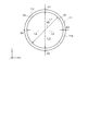
- FIG. 1 is a schematic cross-sectional view illustrating the configuration of an electrostatic chuck according to this embodiment.
- 2A and 2B are schematic plan views illustrating the configuration of the electrode layer.
- FIG. 3 is a schematic plan view illustrating the first positional relationship between the ceramic dielectric substrate and the electrode layer.
- FIG. 4 is a schematic plan view illustrating a second arrangement relationship between the ceramic dielectric substrate and the electrode layer.
- FIG. 5 is a diagram showing the mutual error of the distance between the ceramic dielectric substrate and the electrode layer.
- FIG. 6 is a schematic plan view illustrating the third positional relationship between the ceramic dielectric substrate and the electrode layer.
- FIG. 7 is a diagram showing a first mutual error ratio of the distance between the electrode layers with respect to the outer diameter of the ceramic dielectric substrate.
- FIG. 8 is a diagram showing a second mutual error ratio of the distance between the electrode layers with respect to the outer diameter of the ceramic dielectric substrate.
- FIG. 9 is a diagram illustrating a difference in mutual error in the distance between the ceramic dielectric substrate and the electrode layer.
- FIG. 10 is a diagram showing a third mutual error ratio of the distance between the electrode layers with respect to the outer diameter of the ceramic dielectric substrate.
- FIG. 11 is a diagram illustrating a fourth mutual error ratio of the distance between the electrode layers with respect to the outer diameter of the ceramic dielectric substrate.
- FIG. 12 is a diagram illustrating a fifth mutual error ratio of the distance between the electrode layers with respect to the outer diameter of the ceramic dielectric substrate.
- FIG. 13 is a diagram showing a ratio of mutual errors in the distance between the ceramic dielectric substrate and the electrode layer.
- FIG. 14 is a diagram illustrating the coaxiality between the electrode layer and the ceramic dielectric substrate.
- FIGS. 15A and 15B are schematic plan views showing modifications of the ceramic dielectric substrate and the electrode layer.
- FIG. 16 is a schematic plan view showing another modification of the ceramic dielectric substrate and the electrode layer.
- FIG. 17 is a schematic plan view illustrating still another modification example of the electrode layer.
- FIG. 18 is a schematic plan view illustrating the fourth positional relationship between the ceramic dielectric substrate and the electrode layer.
- FIG. 19 is a diagram illustrating the ratio of the outer peripheral lengths of the ceramic dielectric substrate and the electrode layer.
- FIG. 20 is a diagram showing the ratio of the areas of the ceramic dielectric substrate and the electrode layer.
- FIG. 21 is a schematic enlarged view in which the region A1 shown in FIG. 1 is enlarged.
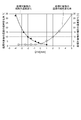
- 22 (a) and 22 (b) show the relationship between the width of the seal ring and the rate of change in the temperature of the object to be processed, and the width of the seal ring and the temperature change at the end of the object to be processed. It is a graph showing the relationship between.
- FIG. 23 is a graph showing the relationship between the overlap distance and the change rate of the temperature of the processing object with time, and the relationship between the overlap distance and the temperature change at the end of the process object. .
- FIGS. 24A to 24C are schematic plan views when the peripheral end portion of the ceramic dielectric substrate is viewed in the direction of the arrow A3 shown in FIG. 25 (a) and 25 (b) show the relationship between the second area ratio of the ceramic dielectric substrate and the electrode layer and the rate of change with time of the temperature of the object to be processed, and the second area ratio. It is a graph showing the relationship between the temperature change of the edge part of a process target object.
- FIG. 26 is a schematic cross-sectional view illustrating the linear distance between the end portion of the seal ring and the end portion of the electrode layer.
- FIG. 27 is a schematic cross-sectional view illustrating an end portion of the seal ring of the present embodiment.
- FIG. 28A and 28B are schematic cross-sectional views for explaining the signs of the linear distance between the end portion of the seal ring and the end portion of the electrode layer.
- FIG. 29 is a graph showing the relationship between the linear distance D14 and the temperature change rate of the object to be processed and the relationship between the linear distance D14 and the temperature change at the end of the object to be processed. It is.
- FIG. 30 is a schematic sectional view showing a wafer processing apparatus according to another embodiment of the present invention.
- a first invention is provided with a first main surface on which a processing object is placed, a second main surface opposite to the first main surface, and a part of the first main surface provided at a peripheral end portion.
- a ceramic dielectric substrate that is a polycrystalline ceramic sintered body, and is interposed between the first main surface and the second main surface of the ceramic dielectric substrate,
- An electrode layer integrally sintered with the ceramic dielectric substrate, and the electrode layer includes a plurality of electrode elements disposed apart from each other, and when viewed in a direction perpendicular to the first main surface, The outer periphery of the ceramic dielectric substrate is processed so that the distance between the outer periphery of the ceramic dielectric substrate and the outer periphery of the electrode layer is uniform, and the outer periphery of the electrode layer and the ceramic dielectric substrate are viewed in the direction.
- the gap between the outer periphery of the plurality of electrode elements is narrower than the gap between the plurality of electrode elements.
- the width of the ring is not less than 0.3 mm and not more than 3 mm, and when viewed in the direction, the width of the electrode layer overlapping the seal ring is not less than ⁇ 0.7 mm and not more than 2 mm. This is an electrostatic chuck.
- this electrostatic chuck According to this electrostatic chuck, a large and constant attracting force can be obtained on the outer peripheral portion of the ceramic dielectric substrate while maintaining the withstand voltage at the outer peripheral portion of the ceramic dielectric substrate.
- the temperature distribution can be made uniform.
- the electrode layer by arranging the electrode layer to a position close to the outer periphery of the ceramic dielectric substrate, the adsorption force at the outer peripheral portion of the ceramic dielectric substrate becomes constant even if the width of the seal ring is narrow.
- the contact area between the wafer and the ceramic dielectric substrate and the adsorption force on the ceramic dielectric substrate are uniform in the circumferential direction, and the rate of change with time of the temperature of the processing object is reduced, It is possible to achieve both reduction of the temperature change at the end.
- a first main surface on which a processing object is placed a second main surface opposite to the first main surface, and a part of the first main surface provided at a peripheral end portion.
- a ceramic dielectric substrate that is a polycrystalline ceramic sintered body, and is interposed between the first main surface and the second main surface of the ceramic dielectric substrate,
- An electrode layer integrally sintered with the ceramic dielectric substrate, and the gap between the outer periphery of the ceramic dielectric substrate and the outer periphery of the electrode layer is uniform when viewed in a direction orthogonal to the first main surface.
- the outer periphery of the ceramic dielectric substrate is processed so that the outer periphery of the electrode layer and the outer periphery of the ceramic dielectric substrate are on a first imaginary line extending from the center of the ceramic dielectric substrate in the outer peripheral direction.
- the mutual error of the interval is 200 micrometers or less
- the width of the seal ring is not less than 0.3 mm and not more than 3 mm, and the width of the electrode layer overlapping the seal ring when viewed in the direction is not less than ⁇ 0.7 mm and not more than 2 mm. This is an electrostatic chuck.
- the outer peripheral portion of the ceramic dielectric substrate is maintained while maintaining the withstand voltage at the outer peripheral portion of the ceramic dielectric substrate.
- a large and constant adsorption force can be obtained, and the temperature distribution of the object to be processed can be made uniform.
- the electrode layer by arranging the electrode layer to a position close to the outer periphery of the ceramic dielectric substrate, the adsorption force at the outer peripheral portion of the ceramic dielectric substrate becomes constant even if the width of the seal ring is narrow.
- the contact area between the wafer and the ceramic dielectric substrate and the adsorption force on the ceramic dielectric substrate are uniform in the circumferential direction, and the rate of change with time of the temperature of the processing object is reduced, It is possible to achieve both reduction of the temperature change at the end.
- a first main surface on which a processing target is placed a second main surface opposite to the first main surface, and a part of the first main surface provided at a peripheral end portion.
- a ceramic dielectric substrate that is a polycrystalline ceramic sintered body, and is interposed between the first main surface and the second main surface of the ceramic dielectric substrate,
- An electrode layer integrally sintered with the ceramic dielectric substrate, and the gap between the outer periphery of the ceramic dielectric substrate and the outer periphery of the electrode layer is uniform when viewed in a direction orthogonal to the first main surface.
- the outer periphery of the ceramic dielectric substrate is processed so that the outer periphery of the electrode layer and the outer periphery of the ceramic dielectric substrate are on a first imaginary line extending from the center of the ceramic dielectric substrate in the outer peripheral direction.
- Interval X1 from the center of the ceramic dielectric substrate An interval between the outer circumference of the electrode layer and the outer circumference of the ceramic dielectric substrate on the second imaginary line extending in the circumferential direction and extending to the opposite side of the first imaginary line is an interval X2,
- the outer diameter at the outer periphery of the electrode layer is an outer diameter X5
- / X5 is 0% or more and 0.07% or less
- the width of the seal ring is 0.3 mm or more and 3 or less.
- the width of the electrode layer overlapping the seal ring when viewed in the direction is not less than ⁇ 0.7 mm and not more than 2 mm.
- the dielectric breakdown voltage at the outer peripheral portion of the ceramic dielectric substrate is maintained and the ceramic is maintained.
- a large and constant attractive force can be obtained on the outer periphery of the dielectric substrate, and the temperature distribution of the object to be processed can be made uniform.
- the electrode layer by arranging the electrode layer to a position close to the outer periphery of the ceramic dielectric substrate, the adsorption force at the outer peripheral portion of the ceramic dielectric substrate becomes constant even if the width of the seal ring is narrow.
- the contact area between the wafer and the ceramic dielectric substrate and the adsorption force on the ceramic dielectric substrate are uniform in the circumferential direction, and the rate of change with time of the temperature of the processing object is reduced, It is possible to achieve both reduction of the temperature change at the end.
- a first main surface on which a processing object is placed a second main surface opposite to the first main surface, and a part of the first main surface provided at a peripheral end portion.
- a ceramic dielectric substrate that is a polycrystalline ceramic sintered body, and is interposed between the first main surface and the second main surface of the ceramic dielectric substrate,
- An electrode layer integrally sintered with the ceramic dielectric substrate, and the gap between the outer periphery of the ceramic dielectric substrate and the outer periphery of the electrode layer is uniform when viewed in a direction orthogonal to the first main surface.
- the outer periphery of the ceramic dielectric substrate is processed so that the outer periphery of the electrode layer and the outer periphery of the ceramic dielectric substrate are on a first imaginary line extending from the center of the ceramic dielectric substrate in the outer peripheral direction.
- the interval is 2 mm or less, and the outer periphery of the electrode layer
- the mutual error of the gap with the outer periphery of the ceramic dielectric substrate is 200 micrometers or less, and the linear distance between the inner peripheral side end of the seal ring and the outer peripheral end of the electrode layer is ⁇ 2
- the contact area between the wafer and the ceramic dielectric substrate and the adsorption force on the ceramic dielectric substrate are uniform in the circumferential direction, and the rate of change with time of the temperature of the processing object is reduced, It is possible to achieve both reduction of the temperature change at the end.
- the electrostatic chuck is characterized in that when the area of the ceramic dielectric substrate is S2, S1 / S2 is -3.4% or more and 5% or less.
- the electrode layer is arranged to a position close to the outer periphery of the ceramic dielectric substrate, so that the adsorption force at the outer peripheral portion of the ceramic dielectric substrate becomes constant even if the width of the seal ring is narrow.
- an interval between the outer periphery of the electrode layer and the outer periphery of the ceramic dielectric substrate is longer than 0 millimeters and not more than 1.95 millimeters.
- the temperature distribution of the object to be processed is made uniform while maintaining the withstand voltage at the outer periphery of the ceramic dielectric substrate. Can be planned.
- LX5 / LX6 is 97.4% or more and 99.6% or less.
- the temperature distribution of the object to be processed can be made uniform while maintaining the withstand voltage at the outer periphery of the ceramic dielectric substrate.
- an area of a circle defined by an outer diameter of the outer periphery of the electrode layer is defined by an area SX5 and an outer diameter of the outer periphery of the ceramic dielectric substrate.
- SX5 / SX6 is 95.1% or more and 99.2% or less when the area of the circle is SX6.
- the temperature distribution of the object to be processed can be made uniform while maintaining the withstand voltage at the outer periphery of the ceramic dielectric substrate.
- the outer periphery of the electrode layer and the ceramic dielectric substrate on the first imaginary line extending from the center of the ceramic dielectric substrate in the outer circumferential direction, the outer periphery of the electrode layer and the ceramic dielectric substrate The outer circumference of the electrode layer on a second imaginary line extending from the center of the ceramic dielectric substrate in the outer circumferential direction and extending to the opposite side to the first imaginary line. And a virtual line extending from the center of the ceramic dielectric substrate to the outer peripheral direction and extending in a direction perpendicular to the first virtual line, the distance between the ceramic dielectric substrate and the outer periphery of the ceramic dielectric substrate being an interval X2.
- this electrostatic chuck According to this electrostatic chuck, a large and constant attracting force can be obtained on the outer peripheral portion of the ceramic dielectric substrate while maintaining the withstand voltage at the outer peripheral portion of the ceramic dielectric substrate.
- the temperature distribution can be made uniform.
- the outer periphery of the electrode layer and the ceramic dielectric substrate on the first imaginary line extending from the center of the ceramic dielectric substrate in the outer peripheral direction, the outer periphery of the electrode layer and the ceramic dielectric substrate The outer circumference of the electrode layer on a second imaginary line extending from the center of the ceramic dielectric substrate in the outer circumferential direction and extending to the opposite side to the first imaginary line. And a virtual line extending from the center of the ceramic dielectric substrate to the outer peripheral direction and extending in a direction perpendicular to the first virtual line, the distance between the ceramic dielectric substrate and the outer periphery of the ceramic dielectric substrate being an interval X2.
- an interval between the outer periphery of the electrode layer and the outer periphery of the ceramic dielectric substrate is an imaginary line extending from the center of the ceramic dielectric substrate toward the outer periphery by an interval X3.
- the distance between the outer periphery of the electrode layer and the outer periphery of the ceramic dielectric substrate is an interval X4 on the fourth imaginary line extending to the opposite side of the imaginary line,
- The electrostatic chuck is characterized in that X3-X4
- the temperature distribution of the object to be processed can be made uniform while maintaining the withstand voltage at the outer periphery of the ceramic dielectric substrate.
- the outer periphery of the electrode layer and the ceramic dielectric substrate on the first imaginary line extending from the center of the ceramic dielectric substrate in the outer peripheral direction, the outer periphery of the electrode layer and the ceramic dielectric substrate The outer circumference of the electrode layer on a second imaginary line extending from the center of the ceramic dielectric substrate in the outer circumferential direction and extending to the opposite side to the first imaginary line. And a virtual line extending from the center of the ceramic dielectric substrate to the outer peripheral direction and extending in a direction perpendicular to the first virtual line, the distance between the ceramic dielectric substrate and the outer periphery of the ceramic dielectric substrate being an interval X2.
- the gap between the outer periphery of the electrode layer and the outer periphery of the ceramic dielectric substrate is an interval X3, an imaginary line extending from the center of the ceramic dielectric substrate toward the outer periphery,
- the interval between the outer periphery of the electrode layer and the outer periphery of the ceramic dielectric substrate is set as an interval X4, and the outer diameter at the outer periphery of the electrode layer is set as an outer diameter X5.
- the electrostatic chuck is characterized in that
- the temperature distribution of the object to be processed can be made uniform while maintaining the withstand voltage at the outer periphery of the ceramic dielectric substrate.
- the outer periphery of the electrode layer and the ceramic dielectric substrate on the first imaginary line extending from the center of the ceramic dielectric substrate in the outer peripheral direction, the outer periphery of the electrode layer and the ceramic dielectric substrate The outer circumference of the electrode layer on a second imaginary line extending from the center of the ceramic dielectric substrate in the outer circumferential direction and extending to the opposite side to the first imaginary line. And a virtual line extending from the center of the ceramic dielectric substrate to the outer peripheral direction and extending in a direction perpendicular to the first virtual line, the distance between the ceramic dielectric substrate and the outer periphery of the ceramic dielectric substrate being an interval X2.
- the gap between the outer periphery of the electrode layer and the outer periphery of the ceramic dielectric substrate is an interval X3, an imaginary line extending from the center of the ceramic dielectric substrate toward the outer periphery,
- the temperature distribution of the object to be processed can be made uniform while maintaining the withstand voltage at the outer periphery of the ceramic dielectric substrate.
- the fifteenth invention is a wafer processing apparatus comprising the electrostatic chuck according to any one of the first to fourteenth inventions.
- the in-plane temperature distribution of the wafer (processing object) becomes uniform, and a predetermined process can be performed without reducing the yield of the wafer (processing object).
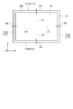
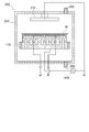
- FIG. 1 is a schematic cross-sectional view illustrating the configuration of an electrostatic chuck according to this embodiment.
- the electrostatic chuck 110 according to this embodiment includes a ceramic dielectric substrate 11 and an electrode layer 12.
- the ceramic dielectric substrate 11 is a flat base material made of, for example, a polycrystalline ceramic sintered body.
- the first main surface 11a on which the processing object W such as a semiconductor wafer is placed and the first main surface 11a are And a second main surface 11b on the opposite side.
- the electrode layer 12 is interposed between the first main surface 11 a and the second main surface 11 b of the ceramic dielectric substrate 11. That is, the electrode layer 12 is formed so as to be inserted into the ceramic dielectric substrate 11.
- the electrode layer 12 is integrally sintered with the ceramic dielectric substrate 11.
- the electrostatic chuck substrate 100 is a plate-like structure including a ceramic dielectric substrate 11 and an electrode layer 12 provided on the ceramic dielectric substrate 11.
- the electrostatic chuck 110 is, for example, a Coulomb electrostatic chuck.
- the volume resistivity of the ceramic dielectric substrate 11 is, for example, 1 ⁇ 10 14 ⁇ ⁇ cm or more.
- the electrostatic chuck 110 applies an attracting and holding voltage 80 to the electrode layer 12 to generate charges on the first main surface 11a side of the electrode layer 12, and attracts and holds the processing object W by electrostatic force.
- the direction connecting the first main surface 11a and the second main surface 11b is the Z direction
- one of the directions orthogonal to the Z direction is the X direction
- the Z direction and the X direction are orthogonal.
- the direction to do is referred to as the Y direction.
- the electrode layer 12 is provided along the first main surface 11 a and the second main surface 11 b of the ceramic dielectric substrate 11.
- the electrode layer 12 is an adsorption electrode for adsorbing and holding the processing object W.
- the electrode layer 12 may be monopolar or bipolar. Further, it may be a tripolar type or other multipolar type. The number and arrangement of the electrode layers 12 are appropriately selected.
- the electrode layer 12 shown in FIG. 1 is a bipolar type, and a bipolar electrode layer 12 is provided on the same surface.
- the ceramic dielectric substrate 11 includes a first dielectric layer 111 between the electrode layer 12 and the first major surface 11a, and a second dielectric layer 112 between the electrode layer 12 and the second major surface 11b.
- the visible light transmittance of at least the first dielectric layer 111 of the ceramic dielectric substrate 11 is preferably greater than 0% and not greater than 3.7%, for example.
- the visible light transmittance is a transmittance when a dielectric having a thickness of 1 millimeter is irradiated with light having a wavelength of about 600 nanometers (nm).
- the visible light transmittance of at least the first dielectric layer 111 in the ceramic dielectric substrate 11 is within the above range, so that the position of the electrode layer 12 provided in the ceramic dielectric substrate 11 is changed to the ceramic dielectric. It can be easily confirmed from the outside of the substrate 11. If the visible light transmittance of the second dielectric layer 112 in the ceramic dielectric substrate 11 is within the above range, the electrode layer is formed from the second main surface 11b side before the ceramic dielectric substrate 11 and the base plate 50 are joined. 12 positions can be confirmed.
- the position of the electrode layer 12 is not measured by using a measurement device unsuitable for fine dimension measurement such as an ultrasonic flaw detector, but X-ray CT or the like is used. It is possible to measure the position of the electrode layer 12 by such a measuring method. However, it is possible to measure the position of the internal electrode layer 12 from the outside of the ceramic dielectric substrate 11 by using a general measuring machine such as a factory microscope, instead of using a measuring device unsuitable for mass production. preferable.
- the position of the electrode layer 12 inside the ceramic dielectric substrate 11 (for example, the position of the outer periphery) can be easily and accurately. Grinding can be performed after measurement. In other words, it is possible to perform processing while correcting misalignment and shrinkage dimension error that may occur. For this reason, in the ceramic dielectric substrate 11 applied in the present embodiment, the distance between the outer periphery of the ceramic dielectric substrate 11 and the outer periphery of the electrode layer 12 is uniform in the Z direction.
- “uniform” means that a manufacturing error is included.
- the “manufacturing error” is, for example, about 200 micrometers ( ⁇ m) or less.
- the electrostatic chuck 110 is mounted on the base plate 50.
- heat-resistant resin such as silicone, indium bonding, brazing, or the like is used.
- the adhesive material is appropriately selected from the viewpoint of operating temperature zone, cost, etc., but a material having a high thermal conductivity is more preferable.
- the base plate 50 is divided into, for example, an aluminum upper part 50a and a lower part 50b, and a communication path 55 is provided between the upper part 50a and the lower part 50b.
- the communication path 55 has one end connected to the input path 51 and the other end connected to the output path 52.
- the base plate 50 serves to adjust the temperature of the electrostatic chuck 110. For example, when cooling the electrostatic chuck 110, a cooling medium flows in from the input path 51, passes through the communication path 55, and flows out from the output path 52. Thereby, the heat of the base plate 50 can be absorbed by the cooling medium, and the electrostatic chuck 110 mounted thereon can be cooled.
- the electrostatic chuck 110 in the case where the electrostatic chuck 110 is kept warm, it is possible to put a heat retaining medium in the communication path 55.
- a heating element can be built in the electrostatic chuck 110 or the base plate 50. As described above, when the temperature of the electrostatic chuck 110 is adjusted via the base plate 50, the temperature of the processing object W attracted and held by the electrostatic chuck 110 can be easily adjusted.
- a convex portion 13 is provided on the first main surface 11 a side of the ceramic dielectric substrate 11 as necessary, and a groove 14 is provided between the convex portions 13.
- the groove 14 is in communication, and a space is formed between the back surface of the processing object W mounted on the electrostatic chuck 110 and the groove 14.
- the introduction path 53 that penetrates the base plate 50 and the ceramic dielectric substrate 11 is connected to the groove 14.
- a transmission gas such as helium (He)
- He helium
- the temperature of the processing target W and the processing target W are attached. Particles can be controlled in a favorable state.
- a connecting portion 20 is provided on the second main surface 11 b of the ceramic dielectric substrate 11.
- a contact electrode 61 is provided on the upper part 50 a of the base plate 50 corresponding to the position of the connecting part 20. Therefore, when the electrostatic chuck 110 is attached to the upper portion 50 a of the base plate 50, the contact electrode 61 comes into contact with the connecting portion 20, and thereby the contact electrode 61 and the electrode layer 12 are electrically connected via the connecting portion 20. It will be.
- a movable probe is used for the contact electrode 61.
- the contact electrode 61 is not limited to the above, and may have any form such as a configuration in which the contact electrode 61 is simply in contact with the connection electrode 20 or a connection electrode 20 that is connected to the connection part 20 by fitting or screwing. .
- the crystal material contained in the ceramic dielectric substrate 11 is, for example, any one of Al 2 O 3 , Y 2 O 3 and YAG. By using this material, the visible light transparency, insulation resistance, and plasma durability of the ceramic dielectric substrate 11 can be enhanced.
- the thickness of the first dielectric layer 111 in the ceramic dielectric substrate 11 is, for example, 100 micrometers or more. When the thickness of the first dielectric layer 111 is 100 micrometers or more, a sufficient withstand voltage in the electrostatic chuck 110 can be maintained. The thickness of the first dielectric layer 111 greatly affects the adsorption force, and can be set as appropriate in order to set the temperature of the processing object W to a desired temperature. In an embodiment, the thickness of the first dielectric layer 111 can be set, for example, from 100 micrometers to 1000 micrometers, more preferably from 100 micrometers to 500 micrometers.
- the thickness of the second dielectric layer 112 of the ceramic dielectric substrate 11 can be set as appropriate.
- the total thickness of the electrostatic chuck substrate 100 in which the electrode layer 12 is provided on the ceramic dielectric substrate 11 is, for example, 0.5 mm to 7 mm in consideration of the mechanical strength and cooling performance of the ceramic dielectric substrate 11. Is preferred.
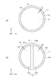
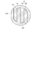
- FIG. 2A and 2B are schematic plan views illustrating the configuration of the electrode layer. 2A and 2B, the outer shapes of the ceramic dielectric substrate 11 and the electrode layer 12 are shown by solid lines for convenience of explanation.
- FIG. 2A shows an example of the unipolar electrode layer 12.
- the electrode layer 12 is provided in a substantially circular shape when viewed in the Z direction.
- the outer shape of the ceramic dielectric substrate 11 viewed in the Z direction is also substantially circular.
- the electrode layer 12 is disposed concentrically with the ceramic dielectric substrate 11.
- FIG. 2B shows an example of the bipolar electrode layer 12.
- the electrode layer 12 includes a first electrode element 121 and a second electrode element 122.
- the first electrode element 121 and the second electrode element 122 are spaced apart from each other.
- Each shape of the first electrode element 121 and the second electrode element 122 is substantially semicircular.
- the first electrode element 121 has a first outer periphery 121r and a first straight side 121s.
- the first outer periphery 121r is a side of an arc portion having a substantially semicircular outer shape.
- the first straight side 121s is a side of a straight part of a substantially semicircular outline.
- the second electrode element 122 has a second outer periphery 122r and a second straight side 122s.
- the second outer periphery 122r is a side of an arc portion having a substantially semicircular outer shape.
- the second straight side 122s is a side of the straight portion of the substantially semicircular outline.
- the first straight side 121s and the second straight side 122s are arranged so as to face each other.
- the outer shape of the electrode layer 12 including the gap between the first electrode element 121 and the second electrode element 122 is substantially circular.
- the ceramic dielectric substrate 11 is ground after firing.
- the outer shape of the ceramic dielectric substrate 11 is formed by grinding the outer periphery while rotating the ceramic dielectric substrate 11.
- the distance d between the outer periphery 11r of the ceramic dielectric substrate 11 and the outer periphery 12r of the electrode layer 12 is provided to be uniform over almost the entire outer periphery 11r.
- the distance d1 between the outer periphery 11r of the ceramic dielectric substrate 11 and the first outer periphery 121r of the first electrode element 121 and the outer periphery 11r of the ceramic dielectric substrate 11 and the second The distance d2 between the electrode element 122 and the second outer periphery 122r is provided to be uniform over the outer periphery 11r. That is, the interval d1 and the interval d2 are uniform over the outer periphery 11r.
- the outer periphery 11r of the ceramic dielectric substrate 11 is ground inside the ceramic dielectric substrate 11 when it is ground. Grinding can be performed accurately while confirming the position of the outer periphery 12r (first outer periphery 121r, second outer periphery 122r) of the electrode layer 12 provided. Thereby, the distances d, d1, and d2 can be formed uniformly over substantially the entire outer periphery 11r.
- the electrode layer 12 having three or more poles examples of the monopolar type and the bipolar type have been described as the electrode layer 12.
- the electrode layer 12 having three or more poles is also applicable.
- the outer shape including the gap between the electrode elements may be provided in a substantially circular shape in the plurality of electrode elements corresponding to each pole.
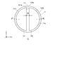
- FIG. 3 is a schematic plan view illustrating the first positional relationship between the ceramic dielectric substrate and the electrode layer.
- the outer shapes of the ceramic dielectric substrate 11 and the electrode layer 12 are shown by solid lines.
- the electrode layer 12 shown in FIG. 3 is a bipolar type, and has a first electrode element 121 and a second electrode element 122.
- the distance between the first straight side 121s of the first electrode element 121 and the second straight side 122s of the second electrode element is defined as a distance ds.
- the interval between the first outer periphery 121r and the outer periphery 11r of the ceramic dielectric substrate 11 is the interval d1
- the interval between the second outer periphery 122r and the outer periphery 11r of the ceramic dielectric substrate 11 is the interval d2. It is.
- the intervals d1 and d2 are narrower than the interval ds. That is, the intervals d1 and d2 are uniform over the outer periphery 11r and are narrower than the interval ds.
- the electrode layer 12 is disposed to a position very close to the outer periphery 11r of the ceramic dielectric substrate 11, and the width of the dielectric (a part of the ceramic dielectric substrate 11) provided outside the electrode layer 12 is increased. Further, the electrode layer 12 can be disposed uniformly below the seal ring 13a (see FIG. 21). Thereby, while maintaining the withstand voltage at the outer peripheral portion of the ceramic dielectric substrate 11, a uniform adsorption force is obtained over a wide range of the object to be processed, and the temperature distribution of the object to be processed is made uniform. Will be able to.
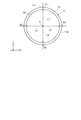
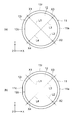
- FIG. 4 is a schematic plan view illustrating a second arrangement relationship between the ceramic dielectric substrate and the electrode layer.
- the outer shapes of the ceramic dielectric substrate 11 and the electrode layer 12 are represented by solid lines.
- the electrode layer 12 shown in FIG. 4 is a monopolar type.
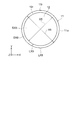
- a first virtual line L1 of a virtual line extending from the center position C of the ceramic dielectric substrate 11 toward the outer periphery 11r is used.
- the interval between the outer periphery 12r of the electrode layer 12 and the outer periphery 11r of the ceramic dielectric substrate 11 is defined as an interval X1.
- the mutual error of the interval X1 is 200 micrometers or less.
- the mutual error of the interval X1 means a mutual error of the interval X1 on each first virtual line L1 when the first virtual lines L1 having different angles with respect to the position C are set.
- the virtual lines extended to the opposite side to the first virtual line L 1 are the second virtual lines.
- One of the virtual lines extended in the direction orthogonal to the virtual line L2 and the first virtual line L1 is a third virtual line L3, and the virtual line extended to the opposite side of the third virtual line L3 is a fourth virtual line L4. .
- the interval between the outer periphery 12r of the electrode layer 12 and the outer periphery 11r of the ceramic dielectric substrate 11 is defined as an interval X2.
- the interval between the outer periphery 12r of the electrode layer 12 and the outer periphery 11r of the ceramic dielectric substrate 11 is defined as an interval X3.
- the interval between the outer periphery 12r of the electrode layer 12 and the outer periphery 11r of the ceramic dielectric substrate 11 is defined as an interval X4.
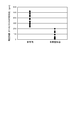
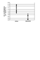
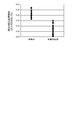
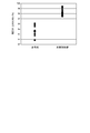
- FIG. 5 is a diagram showing the mutual error of the distance between the ceramic dielectric substrate and the electrode layer.
- FIG. 5 shows the mutual error of the interval in the ceramic dielectric substrate according to the reference example and the mutual error of the interval in the ceramic dielectric substrate 11 according to the present embodiment.
- the ceramic dielectric substrate according to the reference example is obtained by adjusting only the shrinkage of the ceramic dielectric substrate and the electrode layer during sintering.
- the vertical axis represents the mutual error of the distance between the ceramic dielectric substrate 11 and the electrode layer 12.
- the mutual error of the interval is the maximum value among the absolute value of the interval X1 to the interval X2 and the absolute value of the interval X3 to the interval X4.
- the unit is micrometer ( ⁇ m).
- FIG. 5 shows the results of measuring the mutual error of the intervals for 30 samples for each of the reference example and this embodiment.
- the ceramic dielectric substrate according to the reference example has a mutual error of an interval of about 200 micrometers to 520 micrometers.
- the mutual error is an interval of 200 micrometers or less.
- the mutual error in the distance between the outer periphery 11r of the ceramic dielectric substrate 11 and the outer periphery 12r of the electrode layer 12 can be made very small.
- the electrode layer 12 can be formed to a position very close to the outer periphery 11r of the ceramic dielectric substrate 11, and the width of the dielectric (a part of the ceramic dielectric substrate 11) provided outside the electrode layer 12 is also achieved.
- a uniform adsorption force is obtained over a wide range of the object to be processed, and the temperature distribution of the object to be processed is made uniform. Will be able to.
- FIG. 6 is a schematic plan view illustrating the third positional relationship between the ceramic dielectric substrate and the electrode layer.
- the outer shapes of the ceramic dielectric substrate 11 and the electrode layer 12 are shown by solid lines.
- the electrode layer 12 shown in FIG. 6 is a monopolar type.
- the outer diameter at the outer periphery 12r of the electrode layer 12 is defined as an outer diameter X5.
- the outer diameter X5 is an outer diameter when the outermost shape of the electrode layer 12 is assumed to be a circle.
- the outer diameter X5 is the outer circle equivalent diameter of the electrode layer 12.
- / outer diameter X5 is 0% or more and 0.07% or less.
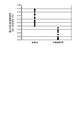
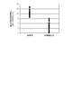
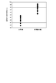
- FIG. 7 is a diagram showing a first mutual error ratio of the distance between the electrode layers with respect to the outer diameter of the ceramic dielectric substrate.
- FIG. 7 shows the ratio of the absolute value of the distance X1 to the distance X2 with respect to the outer diameter X5 in the ceramic dielectric substrate according to the reference example (hereinafter simply referred to as “first mutual error ratio”), and this embodiment.
- the first mutual error rate in the ceramic dielectric substrate 11 according to the above is expressed.
- the ceramic dielectric substrate according to the reference example is obtained by adjusting only the shrinkage of the ceramic dielectric substrate and the electrode layer during sintering.
- FIG. 7 represents the first mutual error ratio (
- the unit is%.
- FIG. 7 shows the result of measuring the first mutual error ratio for 30 samples for each of the reference example and the present embodiment.
- the first mutual error ratio is about 0.08% to 0.180%.
- the first mutual error ratio is 0% or more and 0.07% or less.
- the first mutual error ratio of the distance between the electrode layers 12 with respect to the outer diameter of the ceramic dielectric substrate 11 can be made extremely small.
- the electrode layer 12 can be formed to a position very close to the outer periphery 11r of the ceramic dielectric substrate 11 with the outer diameter X5 of the electrode layer 12 as a reference, and a dielectric provided outside the electrode layer 12 ( The width of part of the ceramic dielectric substrate 11) can be made uniform, and the electrode layer 12 can be evenly arranged below the seal ring 13a.
- the interval d1 between the first outer periphery 121r and the outer periphery 11r and the interval d2 between the second outer periphery 122r and the outer periphery 11r are longer than 0 millimeters and 1.95 millimeters or less. It may be. More preferably, the distance d1 and the distance d2 may be 1.45 millimeters or less, and more preferably 0.95 millimeters or less. In the second to third arrangement relationships described above, the distances X1 to X4 between the outer periphery 12r of the electrode layer 12 and the outer periphery 11r of the ceramic dielectric substrate 11 are longer than 0 millimeters and not more than 1.95 millimeters. May be. More preferably, the intervals X1 to X4 may be 1.45 millimeters or less, and more preferably 0.95 millimeters or less.
- the electrode layer 12 is provided to a position very close to the outer periphery 11r of the ceramic dielectric substrate 11.
- the processing object W can be uniformly adsorbed in a wide range. Therefore, the temperature distribution of the processing object W when adsorbed can be made uniform.
- an electrostatic chuck can be provided.
- FIG. 8 is a diagram showing a second mutual error ratio of the distance between the electrode layers with respect to the outer diameter of the ceramic dielectric substrate.
- the second mutual error ratio of the distance between the electrode layers 12 with respect to the outer diameter of the ceramic dielectric substrate 11 will be described with reference to FIG.
- FIG. 8 shows the ratio of the absolute value of the interval X1 to the interval X3 with respect to the outer diameter X5 in the ceramic dielectric substrate according to the reference example (hereinafter simply referred to as “second mutual error ratio”), and this embodiment.
- the second mutual error ratio in the ceramic dielectric substrate 11 according to the above is expressed.
- the ceramic dielectric substrate according to the reference example is obtained by adjusting only the shrinkage of the ceramic dielectric substrate and the electrode layer during sintering.
- FIG. 8 is the second mutual error ratio (
- the unit is%.
- FIG. 8 shows the results of measuring the second mutual error ratio for 30 samples for each of the reference example and the present embodiment.
- the second mutual error ratio is about 0.08% to 0.180%.
- the second mutual error ratio is 0% or more and 0.07% or less.
- the second mutual error ratio of the distance between the electrode layers 12 with respect to the outer diameter of the ceramic dielectric substrate 11 can be made extremely small.
- the electrode layer 12 can be formed to a position very close to the outer periphery 11r of the ceramic dielectric substrate 11 with the outer diameter X5 of the electrode layer 12 as a reference, and a dielectric provided outside the electrode layer 12 ( The width of a part of the ceramic dielectric substrate 11) can be made uniform, and the electrode layer 12 can be evenly arranged below the seal ring 13a.
- the second mutual error ratio may be expressed as a ratio of the absolute value of the interval X1 to the interval X4 with respect to the outer diameter X5 on the ceramic dielectric substrate (
- FIG. 9 is a diagram illustrating a difference in mutual error in the distance between the ceramic dielectric substrate and the electrode layer.
- FIG. 9 shows a difference in mutual error in the ceramic dielectric substrate according to the reference example and a difference in mutual error in the ceramic dielectric substrate 11 according to the present embodiment.
- the ceramic dielectric substrate according to the reference example is obtained by adjusting only the shrinkage of the ceramic dielectric substrate and the electrode layer during sintering.
- the vertical axis represents the difference in mutual error between the ceramic dielectric substrate 11 and the electrode layer 12.
- the difference between the mutual errors of the intervals is the absolute value of the difference between the absolute value of the interval X1 ⁇ interval X2 and the absolute value of the interval X3 ⁇ interval X4 (
- the unit is micrometer ( ⁇ m).
- FIG. 9 shows the results of measuring the difference in mutual error for 30 samples for each of the reference example and this embodiment. As shown in FIG. 9, in the ceramic dielectric substrate according to the reference example, the difference in mutual error is about 235 micrometers or more and 525 micrometers or less. On the other hand, in the ceramic dielectric substrate 11 according to the present embodiment, the difference in mutual error is from 0 to 200 micrometers.
- the difference in the mutual error in the distance between the ceramic dielectric substrate 11 and the electrode layer 12 can be made very small.
- the electrode layer 12 can be formed to a position very close to the outer periphery 11r of the ceramic dielectric substrate 11 with the outer diameter X5 of the electrode layer 12 as a reference, and a dielectric provided outside the electrode layer 12 ( The width of part of the ceramic dielectric substrate 11) can be made uniform, and the electrode layer 12 can be evenly arranged below the seal ring 13a.
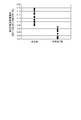
- FIG. 10 is a diagram showing a third mutual error ratio of the distance between the electrode layers with respect to the outer diameter of the ceramic dielectric substrate.
- FIG. 10 shows the ratio (
- the ceramic dielectric substrate according to the reference example is obtained by adjusting only the shrinkage of the ceramic dielectric substrate and the electrode layer during sintering.
- the vertical axis of FIG. 10 is the third mutual error ratio (
- the unit is%.
- FIG. 10 shows the results of measuring the third mutual error ratio for 30 samples for each of the reference example and the present embodiment.
- the ceramic dielectric substrate according to the reference example has a third mutual error ratio of about 0.08% to 0.18%.
- the third mutual error ratio is 0% or more and 0.07% or less.
- the third mutual error ratio of the distance between the electrode layers 12 with respect to the outer diameter of the ceramic dielectric substrate 11 can be made extremely small.
- the electrode layer 12 can be formed to a position very close to the outer periphery 11r of the ceramic dielectric substrate 11 with the outer diameter X5 of the electrode layer 12 as a reference, and a dielectric provided outside the electrode layer 12 ( The width of part of the ceramic dielectric substrate 11) can be made uniform, and the electrode layer 12 can be evenly arranged below the seal ring 13a.
- FIG. 11 is a diagram illustrating a fourth mutual error ratio of the distance between the electrode layers with respect to the outer diameter of the ceramic dielectric substrate.
- a fourth mutual error ratio of the distance between the electrode layers 12 with respect to the outer diameter of the ceramic dielectric substrate 11 will be described.
- FIG. 11 shows the ratio of the absolute value of the distance X1 + the distance X3 to the outer diameter X5 in the ceramic dielectric substrate according to the reference example (hereinafter simply referred to as “fourth mutual error ratio”), and the present embodiment.
- the fourth mutual error ratio in the ceramic dielectric substrate 11 is expressed.
- the ceramic dielectric substrate according to the reference example is obtained by adjusting only the shrinkage of the ceramic dielectric substrate and the electrode layer during sintering.
- the vertical axis of FIG. 11 represents a fourth mutual error ratio (
- the unit is%.
- FIG. 11 shows the result of measuring the fourth mutual error ratio for 30 samples for each of the reference example and this embodiment.
- the ceramic dielectric substrate according to the reference example has a fourth mutual error ratio of about 0.16% to 0.27%.
- the fourth mutual error ratio is 0% or more and 0.15% or less.
- the fourth mutual error ratio can be made very small.
- the electrode layer 12 can be formed to a position very close to the outer periphery 11r of the ceramic dielectric substrate 11 with the outer diameter X5 of the electrode layer 12 as a reference, and a dielectric provided outside the electrode layer 12 ( The width of part of the ceramic dielectric substrate 11) can be made uniform, and the electrode layer 12 can be evenly arranged below the seal ring 13a.
- FIG. 12 is a diagram illustrating a fifth mutual error ratio of the distance between the electrode layers with respect to the outer diameter of the ceramic dielectric substrate.
- the fifth mutual error ratio of the distance between the electrode layers 12 with respect to the outer diameter of the ceramic dielectric substrate 11 will be described with reference to FIG.
- FIG. 12 shows the ratio of the absolute value of the distance X1 ⁇ the distance X3 to the outer diameter X5 in the ceramic dielectric substrate according to the reference example (hereinafter simply referred to as “fifth mutual error ratio”), and this embodiment.
- the fifth mutual error ratio in the ceramic dielectric substrate 11 according to the above is expressed.
- the ceramic dielectric substrate according to the reference example is obtained by adjusting only the shrinkage of the ceramic dielectric substrate and the electrode layer during sintering.
- the vertical axis in FIG. 12 represents a fifth mutual error ratio (
- the unit is%.
- FIG. 12 shows the result of measuring the fifth mutual error ratio for 30 samples for each of the reference example and the present embodiment.
- the ceramic dielectric substrate according to the reference example has a fifth mutual error ratio of about 16% to 27%.
- the fifth mutual error ratio is 15% or less.
- the fifth mutual error ratio of the distance between the electrode layers 12 with respect to the outer diameter of the ceramic dielectric substrate 11 can be made extremely small.
- the electrode layer 12 can be formed to a position very close to the outer periphery 11r of the ceramic dielectric substrate 11 with the outer diameter X5 of the electrode layer 12 as a reference, and a dielectric provided outside the electrode layer 12 ( The width of part of the ceramic dielectric substrate 11) can be made uniform, and the electrode layer 12 can be evenly arranged below the seal ring 13a.
- FIG. 13 is a diagram showing a ratio of mutual errors in the distance between the ceramic dielectric substrate and the electrode layer.
- the ratio of the mutual error of the distance between the ceramic dielectric substrate 11 and the electrode layer 12 will be described with reference to FIG.
- FIG. 13 shows the ratio of the mutual error of the interval in the ceramic dielectric substrate according to the reference example and the ratio of the mutual error of the interval in the ceramic dielectric substrate 11 according to the present embodiment.
- the ceramic dielectric substrate according to the reference example is obtained by adjusting only the shrinkage of the ceramic dielectric substrate and the electrode layer during sintering.
- the vertical axis in FIG. 13 is the ratio of the mutual error in the distance between the ceramic dielectric substrate 11 and the electrode layer 12.
- the ratio of the mutual error of the interval is the ratio of the absolute value of the interval X1 to the interval X2 to the absolute value of the interval X3 to the interval X4 (
- the ratio of the mutual error of the interval is a dimensionless number.
- FIG. 13 shows the results of measuring the ratio of the mutual error for 30 samples for each of the reference example and this embodiment. As shown in FIG. 13, the ceramic dielectric substrate according to the reference example has a mutual error ratio of about 230 to 520. On the other hand, the ceramic dielectric substrate 11 according to the present embodiment has a mutual error ratio of 0 or more and 200 or less.
- the ratio of mutual errors can be made very small.
- the electrode layer 12 can be formed to a position very close to the outer periphery 11r of the ceramic dielectric substrate 11 with the outer diameter X5 of the electrode layer 12 as a reference, and a dielectric provided outside the electrode layer 12 ( The width of part of the ceramic dielectric substrate 11) can be made uniform, and the electrode layer 12 can be evenly arranged below the seal ring 13a. Thereby, while maintaining the withstand voltage at the outer peripheral portion of the ceramic dielectric substrate 11, a uniform adsorption force is obtained over a wide range of the object to be processed, and the temperature distribution of the object to be processed is made uniform. Will be able to.
- FIG. 14 is a diagram illustrating the coaxiality between the electrode layer and the ceramic dielectric substrate.
- the coaxiality between the electrode layer and the ceramic dielectric substrate will be described with reference to FIG.
- FIG. 14 shows the coaxiality between the electrode layer and the ceramic dielectric substrate in the ceramic dielectric substrate according to the reference example, and the electrode layer and the ceramic dielectric substrate in the ceramic dielectric substrate 11 according to the present embodiment.
- the degree of coaxiality between is expressed.
- the coaxiality between the electrode layer and the ceramic dielectric substrate (hereinafter simply referred to as “coaxiality”) refers to the amount of deviation between the center position of the electrode layer and the center position of the ceramic dielectric substrate.
- the ceramic dielectric substrate according to the reference example is obtained by adjusting only the shrinkage of the ceramic dielectric substrate and the electrode layer during sintering.
- shaft of FIG. 14 is a coaxial degree.
- the unit is micrometer ( ⁇ m).
- FIG. 14 shows the results of measuring the coaxiality of 30 samples for each of the reference example and the present embodiment. As shown in FIG. 14, in the reference example, the coaxiality is about 230 micrometers or more and 520 micrometers or less. On the other hand, in this embodiment, the coaxiality is 200 micrometers or less. In FIG. 14, the above-mentioned coaxiality is measured in an electrode layer within 3 millimeters (mm) from the outer diameter of the ceramic dielectric substrate.
- the coaxiality of the ceramic dielectric substrate 11 and the electrode layer 12 can be made extremely small.
- the electrode layer 12 can be formed to a position very close to the outer periphery 11r of the ceramic dielectric substrate 11 with the outer diameter X5 of the electrode layer 12 as a reference, and a dielectric provided outside the electrode layer 12 ( The width of part of the ceramic dielectric substrate 11) can be made uniform, and the electrode layer 12 can be evenly arranged below the seal ring 13a.
- FIGS. 15A and 15B are schematic plan views showing modifications of the ceramic dielectric substrate and the electrode layer.
- FIG. 15A is a schematic plan view for explaining a modification of the electrode layer.
- FIG. 15B is a schematic plan view for explaining a modification of the ceramic dielectric substrate.
- an orientation flat (orientation flat) portion 12 c may be provided on a part of the outer periphery 12 r of the electrode layer 12.
- the interval d described above with reference to FIG. 2A, the interval d1 and interval d2 described above with reference to FIG. 2B, the interval d1 and interval d2 described above with reference to FIG. 3, the interval X1 described above with reference to FIG. X2, the interval X3, and the interval X4, and the interval X1, the interval X2, the interval X3, and the interval X4 described above with reference to FIG. 6 are intervals measured in a portion excluding the portion where the orientation flat portion 12c is provided. .
- the orientation flat portion 11c may be provided on a part of the outer periphery 11r of the ceramic dielectric substrate 11, and the orientation flat portion 12c may be provided on a part of the outer periphery 12r of the electrode layer 12.
- the interval d described above with reference to FIG. 2A, the interval d1 and interval d2 described above with reference to FIG. 2B, the interval d1 and interval d2 described above with reference to FIG. 3, the interval X1 described above with reference to FIG. X2, the interval X3, and the interval X4, and the interval X1, the interval X2, the interval X3, and the interval X4 described above with reference to FIG. 6 are intervals measured in a portion excluding the portion where the orientation flat portion 11c and the orientation flat portion 12c are provided.
- FIG. 16 is a schematic plan view showing another modification of the ceramic dielectric substrate and the electrode layer.
- the ceramic dielectric substrate 11 may have a rectangular shape when viewed in the Z direction.
- the electrode layer 12 may have a rectangular shape.
- a virtual line extending perpendicularly from the center position C of the ceramic dielectric substrate 11 to the first side 114r of the outer periphery 11r is defined as a first virtual line L1.
- a virtual line extending perpendicularly from the center position C of the ceramic dielectric substrate 11 to the second side 115r of the outer periphery 11r is defined as a second virtual line L2.
- a virtual line extending perpendicularly from the center position C of the ceramic dielectric substrate 11 to the third side 116r of the outer periphery 11r is defined as a third virtual line L3.
- a virtual line extending perpendicularly from the center position C of the ceramic dielectric substrate 11 to the fourth side 117r of the outer periphery 11r is defined as a fourth virtual line L4.
- the second side 115r is a side parallel to the first side 114r.
- the third side 116r is a side that intersects the first side 114r and the second side 115r.
- the fourth side 117r is a side that intersects the first side 114r and the second side 115r.
- the interval X2 described above with reference to FIGS. 4 and 6 is assumed to be the interval between the outer periphery 12r of the electrode layer 12 and the outer periphery 11r of the ceramic dielectric substrate 11 on the second virtual line L2.
- the interval X3 described above with reference to FIGS. 4 and 6 is assumed to be the interval between the outer periphery 12r of the electrode layer 12 and the outer periphery 11r of the ceramic dielectric substrate 11 on the first virtual line L3.
- the interval X4 described above with reference to FIGS. 4 and 6 is assumed to be the interval between the outer periphery 12r of the electrode layer 12 and the outer periphery 11r of the ceramic dielectric substrate 11 on the first virtual line L4.
- FIG. 17 is a schematic plan view illustrating still another modification example of the electrode layer.
- the electrode layer 12 illustrated in FIG. 17 is a bipolar electrode layer, and includes a first electrode element 121 and a second electrode element 122. As shown in FIG. 17, each of the first electrode element 121 and the second electrode element 122 has a comb shape.
- the first electrode element 121 and the second electrode element 122 are arranged so that the comb teeth of the first electrode element 121 mesh with the comb teeth of the second electrode element.
- An orientation flat portion 122c is provided in a part of the second outer periphery 122r of the second electrode element 122.
- the orientation flat portion may be provided not on the second electrode element 122 but on the first electrode element 121.
- the outer diameter X5 described above with reference to FIG. 6 is at least one of the first outer periphery 121r of the first electrode element 121 and the second outer periphery 122r of the second electrode element 122. Corresponds to the outer diameter.
- the shape of the electrode layer 12 is not particularly limited.
- FIG. 18 is a schematic plan view illustrating the fourth positional relationship between the ceramic dielectric substrate and the electrode layer.
- the outer shapes of the ceramic dielectric substrate 11 and the electrode layer 12 are represented by solid lines.
- the electrode layer 12 shown in FIG. 18 is a monopolar type.
- the outer diameter at the outer periphery 12r of the electrode layer 12 is defined as an outer diameter X5.
- the outer diameter X5 is an outer diameter when the outermost shape of the electrode layer 12 is assumed to be a circle.
- the outer diameter X5 is the outer circle equivalent diameter of the electrode layer 12.
- the length of the outer periphery 12r defined by the outer diameter X5 is defined as a peripheral length LX5.
- An area of a circle defined by the outer diameter X5 is defined as an area SX5.
- the outer diameter at the outer periphery 11r of the ceramic dielectric substrate 11 is defined as an outer diameter X6.
- the length of the outer periphery 11r defined by the outer diameter X6 is defined as a peripheral length LX6.
- An area of a circle defined by the outer diameter X6 is defined as an area SX6.
- FIG. 19 is a diagram illustrating the ratio of the outer peripheral lengths of the ceramic dielectric substrate and the electrode layer.
- FIG. 19 shows the ratio of the peripheral length LX5 to the peripheral length LX6 (hereinafter simply referred to as “peripheral ratio”) in the ceramic dielectric substrate according to the reference example, and the ceramic dielectric substrate 11 according to the present embodiment.
- the circumference ratio is expressed as follows.
- the ceramic dielectric substrate according to the reference example is obtained by adjusting only the shrinkage of the ceramic dielectric substrate and the electrode layer during sintering.
- FIG. 19 is the circumference ratio (LX5 / LX6) of the ceramic dielectric substrate 11 and the electrode layer 12.
- the vertical axis in FIG. The unit is%.
- FIG. 19 shows the results of measuring the circumference ratio of 30 samples for each of the reference example and this embodiment.
- the ceramic dielectric substrate according to the reference example has a circumference ratio of about 92.8% to 96.1%.
- the circumference ratio is 97.4% or more and 99.6% or less.
- the peripheral length ratio between the ceramic dielectric substrate 11 and the electrode layer 12 can be made very large.
- the electrode layer 12 can be formed to a position very close to the outer periphery 11r of the ceramic dielectric substrate 11 with the outer diameter X5 of the electrode layer 12 as a reference, and a dielectric provided outside the electrode layer 12 ( The width of part of the ceramic dielectric substrate 11) can be made uniform, and the electrode layer 12 can be evenly arranged below the seal ring 13a.
- FIG. 20 is a diagram showing the ratio of the areas of the ceramic dielectric substrate and the electrode layer.
- FIG. 20 shows the ratio of the area SX5 to the area SX6 in the ceramic dielectric substrate according to the reference example (hereinafter simply referred to as “first area ratio”) and the ceramic dielectric substrate 11 according to the present embodiment.
- the first area ratio is expressed.
- the ceramic dielectric substrate according to the reference example is obtained by adjusting only the shrinkage of the ceramic dielectric substrate and the electrode layer during sintering.
- FIG. 20 is the first area ratio (SX5 / SX6) of the ceramic dielectric substrate 11 and the electrode layer 12.
- the vertical axis in FIG. The unit is%.
- FIG. 20 shows the results of measuring the first area ratio for 30 samples for each of the reference example and this embodiment.
- the first area ratio is about 90.8% to 94.6%.
- the first area ratio is 95.1% or more and 99.2% or less.
- the first area ratio of the ceramic dielectric substrate 11 and the electrode layer 12 can be greatly increased.
- the electrode layer 12 can be formed to a position very close to the outer periphery 11r of the ceramic dielectric substrate 11 with the outer diameter X5 of the electrode layer 12 as a reference, and a dielectric provided outside the electrode layer 12 ( The width of part of the ceramic dielectric substrate 11) can be made uniform, and the electrode layer 12 can be evenly arranged below the seal ring 13a.
- FIG. 21 is a schematic enlarged view in which the region A1 shown in FIG. 1 is enlarged.
- the electrostatic chuck 110 according to the present embodiment is, for example, a Coulomb electrostatic chuck.
- the Coulomb type electrostatic chuck an attractive force is generated only on the electrode layer 12. For this reason, it is desirable to dispose the electrode layer 12 to a position close to the outer periphery 11r of the ceramic dielectric substrate 11.
- the electrode layer 12 is placed on the outer periphery 11 r of the ceramic dielectric substrate 11. Can be formed to a position close to. Therefore, the width D1 of the convex portion 13 (seal ring 13a) provided at the peripheral end portion of the ceramic dielectric substrate 11 can be further reduced.
- the seal ring 13 a suppresses the transmission gas such as helium (He) from leaking from the space provided between the processing object W and the groove 14.
- the width D1 of the seal ring 13a is smaller, the area where the processing object W comes into contact with the seal ring 13a becomes smaller. Then, the total amount of wear caused by the friction between the seal ring 13a and the object to be processed W during use of the electrostatic chuck 110 can be suppressed. Thereby, the time-dependent change of the seal ring 13a can be suppressed. Furthermore, particles adhering to the processing object W can also be suppressed.
- a transmission gas such as helium (He) leaks from the space provided between the processing object W and the groove 14. Can be further suppressed. That is, it is possible to control the seal ring 13a more easily by suppressing the variation in the leakage amount of the transmission gas such as helium (He) caused by the manufacturing variation of the seal ring 13a.
- suction of the process target object W in the part in which the seal ring 13a was provided can be stabilized. Therefore, it is possible to maintain a state in which the temperature of the processing object W does not change throughout the process. Thereby, uniform adsorption force is obtained over a wide range of the processing object W, and the temperature distribution of the processing object W when adsorbed can be made uniform.
- the seal ring 13a will be further described with reference to the drawings.
- FIG. 22 (a) and 22 (b) show the relationship between the width of the seal ring and the rate of change in the temperature of the object to be processed, and the width of the seal ring and the temperature change at the end of the object to be processed. It is a graph showing the relationship between.
- FIG. 22A shows a relationship between the width of the seal ring and the rate of change of the temperature of the processing object with time, the width of the seal ring, and the processing object in the electrostatic chuck according to the present embodiment. It is a graph showing the relationship between the temperature change of an edge part.
- FIG. 22A shows a relationship between the width of the seal ring and the rate of change of the temperature of the processing object with time, the width of the seal ring, and the processing object in the electrostatic chuck according to the present embodiment. It is a graph showing the relationship between the temperature change of an edge part.
- 22B shows the relationship between the width of the seal ring and the rate of change with time of the temperature of the object to be processed and the seal ring in the electrostatic chuck according to the present embodiment and the electrostatic chuck according to the comparative example. It is a graph showing the relationship between the width
- the horizontal axis represents the width D1 (mm) of the seal ring 13a.
- the left vertical axis of the graphs shown in FIGS. 22A and 22B is the rate of change (%) of the temperature of the processing object W with time.
- the right vertical axis of the graphs shown in FIG. 22A and FIG. 22B is the temperature change (%) at the end of the object W to be processed.
- FIGS. 22A and 22B are graphs after 100 hours from the start of processing. 22A and 22B, it is assumed that the difference (D1 ⁇ D2) between the width D1 of the seal ring 13a and the overlap distance D2 is 1.0 millimeter. Details of the overlap distance D2 will be described later.
- the rate of change with time of the temperature of the object to be processed W is the surface of the contact surface 13b (see FIG. 21) of the seal ring 13a with the object to be processed W in the plasma environment under the use conditions of the electrostatic chuck 110. It means that the temperature of the object to be processed W changes as the state changes and the heat transfer coefficient changes. Alternatively, “the rate of change with time of the temperature of the processing object W” refers to the average temperature at the center of the processing object W and the portion Wa (end part) of the processing object W that protrudes outside the seal ring 13a. Or the ratio between the temperature of the outer periphery).
- the temperature change at the end of the object to be processed W means that the effect of suppressing the temperature rise of the portion Wa of the object to be processed W outside the seal ring 13a changes according to the width D1 of the seal ring 13a.
- the “temperature change at the end of the processing object W” refers to the rate of increase in the temperature of the portion Wa of the processing object W with respect to the average temperature at the center of the processing object W.
- the width D1 of the seal ring 13a when the width D1 of the seal ring 13a is relatively small, the area of the contact surface 13b of the seal ring 13a becomes relatively small. The rate of change with time of the temperature of the processing object W when the transmission rate changes is relatively small. Further, when the width D1 of the seal ring 13a is relatively small, the contact area between the contact surface 13b and the object to be processed W becomes small, so that the amount of adhering particles can be reduced. On the other hand, if the width D1 of the seal ring 13a is relatively large, the area of the contact surface 13b is relatively wide, and therefore the temperature rise of the portion Wa of the processing object W is relatively low.
- the width D1 of the seal ring 13a is relatively large, the temperature change at the end of the processing object W is relatively small, but the contact area between the contact surface 13b and the processing object W increases, and thus the processing object The amount of particles adhering to W increases. Also, if the width D1 of the seal ring 13a is wide, the dielectric surface, which is the contact surface with the wafer, is easily consumed by plasma during the process, the wafer temperature fluctuates due to changes in the dielectric surface state, and the dielectric surface and the wafer The gas flow rate enclosed between the two changes. This leads to a shortened life of the expected electrostatic chuck.
- the inventor considers the lower limit of the allowable value at which the processing target W can be cooled and the boundary where the heat transfer coefficient between the processing target W and the ceramic dielectric substrate 11 can be changed. It was set as a threshold value that the ratio between the average temperature of the center part of the target object W and the temperature of the part Wa of the process target object W was 10% or less. According to the knowledge obtained by the present inventor, the portion Wa of the processing object W is more susceptible to change with time than the central part of the processing object W. When the ratio between the average temperature of the central portion of the processing object W and the temperature of the portion Wa of the processing object W is 10% or less, a decrease in the process yield of the processing object W can be suppressed.
- the fall of the process yield of the process target object W can be suppressed as the rate of temperature increase of the part Wa of the process target object W with respect to the average temperature of the center part of the process target object W is 10% or less.
- the width D1 of the seal ring 13a is not less than 0.3 millimeters and not more than 3.0 millimeters. Note that the width D1 of the seal ring 13a of 0.3 mm or more and 3.0 mm or less includes a C surface (chamfering) of 1 mm at the maximum at the end of the seal ring 13a.
- the difference (D1-D2) in the electrostatic chucks according to the first comparative example and the second comparative example shown in FIG. 22B is greater than the difference (D1-D2) in the electrostatic chuck 110 according to the present embodiment.
- the temperature change of the portion Wa of the processing object W in the electrostatic chuck according to the first comparative example and the second comparative example is related to the present embodiment. It is larger than the temperature change of the portion Wa of the processing object W in the electrostatic chuck 110.
- a region A2 illustrated in FIG. 22B represents a temperature change range of the portion Wa of the processing target W in the first comparative example and the second comparative example. According to this, in the electrostatic chuck 110 according to the present embodiment, compared with the electrostatic chucks according to the first comparative example and the second comparative example, the portion Wa of the processing object W can be efficiently cooled. Can do.
- FIG. 23 is a graph showing the relationship between the overlap distance and the change rate of the temperature of the processing object with time, and the relationship between the overlap distance and the temperature change at the end of the process object.
- the horizontal axis of the graph shown in FIG. 23 is the overlap distance D2 (mm).
- the left vertical axis of the graph shown in FIG. 23 is the rate of change (%) of the temperature of the processing object W with time.
- the right vertical axis of the graph shown in FIG. 23 is the temperature change (%) at the end of the processing object W.
- the overlapping distance D2 means a distance (width) at which the electrode layer 12 overlaps the seal ring 13a when viewed in the Z direction (see FIG. 21).
- the rate of change with time of the temperature of the processing object W is as described above with reference to FIGS. 22 (a) and 22 (b).
- the “temperature change at the end of the processing object W” is as described above with reference to FIGS. 22 (a) and 22 (b).
- the inventor has a ratio between the average temperature of the central portion of the processing object W and the temperature of the portion Wa of the processing object W of 10%.
- the following was set as a threshold.
- the overlap distance D2 is not less than ⁇ 0.7 millimeters and not more than 2.0 millimeters.
- the negative overlap distance D2 represents a state in which the electrode layer 12 is separated from the seal ring 13a without overlapping when viewed in the Z direction.
- FIGS. 24A to 24C are schematic plan views when the peripheral end portion of the ceramic dielectric substrate is viewed in the direction of the arrow A3 shown in FIG.
- FIG. 24A is a schematic plan view for explaining the area of the region where the electrode layer 12 overlaps the seal ring 13a.
- FIG. 24B is a schematic plan view for explaining the outer diameter of the electrode layer 12.
- FIG. 24C is a schematic plan view illustrating the inner diameter of the seal ring 13a.
- the outer shapes of the ceramic dielectric substrate 11 and the electrode layer 12 are shown by solid lines for convenience of explanation.
- the outer diameter of the electrode layer 12 is defined as an outer diameter D11.
- the area of the region where the electrode layer 12 overlaps the seal ring 13a is defined as area S1.
- the area of the region between the outer diameter end portion of the electrode layer 12 and the end portion on the center side of the seal ring 13a is represented by an area ⁇ S1.
- the area (total area) of the ceramic dielectric substrate 11 when viewed in the Z direction is defined as area S2.
- the outermost circle equivalent diameter of the electrode layer 12 is defined as the first outer diameter D ⁇ b> 11.
- the circle-equivalent diameter at the innermost position among the end portions of the electrode layer 12 is set as the second outer diameter D12.
- the equivalent circle diameter at the innermost position of the inner end of the seal ring 13a is defined as an inner diameter D13.
- the outer diameter D11 of the electrode layer 12 is measured using an ultrasonic flaw detector. Based on the outer diameter D11 measured using the ultrasonic flaw detector, the area S1 of the region where the electrode layer 12 overlaps the seal ring 13a is calculated.
- FIG. 25 (a) and 25 (b) show the relationship between the second area ratio of the ceramic dielectric substrate and the electrode layer and the rate of change with time of the temperature of the object to be processed, and the second area ratio. It is a graph showing the relationship between the temperature change of the edge part of a process target object.
- FIG. 25A shows the relationship between the second area ratio of the ceramic dielectric substrate 11 and the electrode layer 12 and the rate of change with time of the temperature of the processing object in the electrostatic chuck according to the present embodiment. It is a graph showing the relationship between the 2nd area ratio and the temperature change of the edge part of a process target object.
- FIG. 25B shows the relationship between the second area ratio and the rate of change of the temperature of the processing object with time, the second area ratio, and the processing object in the electrostatic chuck according to the comparative example. It is a graph showing the relationship between the temperature change of the edge part of this.
- the horizontal axes of the graphs shown in FIGS. 25A and 25B are the ratio of the area S1 to the area S2 (hereinafter simply referred to as “second area ratio”).
- the left vertical axis of the graphs shown in FIGS. 25A and 25B is the rate of change (%) with time of the temperature of the object W to be processed.
- the right vertical axis of the graphs shown in FIG. 25A and FIG. 25B is the temperature change (%) at the end of the processing object W.
- the rate of change with time of the temperature of the processing object W is as described above with reference to FIGS. 22 (a) and 22 (b).
- the “temperature change at the end of the processing object W” is as described above with reference to FIGS. 22 (a) and 22 (b).
- the inventor has a ratio between the average temperature of the central portion of the processing object W and the temperature of the portion Wa of the processing object W of 10%.
- the following was set as a threshold.
- the second area ratio (S1 / S2) of the electrostatic chuck 110 according to the present embodiment is ⁇ 3.4% or more and 5% or less.
- the width D1 of the seal ring 13a needs to be increased. Therefore, as illustrated in FIG. 25B, the rate of change with time of the temperature of the processing object W in the electrostatic chuck according to the comparative example is the temperature change rate of the processing object W in the electrostatic chuck 110 according to the present embodiment. Greater than rate of change over time. Therefore, in the comparative example shown in FIG. 25B, when the second area ratio is 5%, the ratio between the average temperature of the central portion of the processing object W and the temperature of the portion Wa of the processing object W. Is higher than 10%.
- FIG. 26 is a schematic cross-sectional view illustrating the linear distance between the end portion of the seal ring and the end portion of the electrode layer.
- FIG. 27 is a schematic cross-sectional view illustrating an end portion of the seal ring of the present embodiment.
- FIGS. 28A and 28B are schematic cross-sectional views for explaining the signs of the linear distance between the end portion of the seal ring and the end portion of the electrode layer.
- FIG. 26, FIG. 28A and FIG. 28B correspond to schematic enlarged views in which the region A1 shown in FIG. 1 is enlarged.
- FIG. 28A shows a case where the sign of the linear distance between the end of the seal ring and the end of the electrode layer is positive (+).
- FIG. 28B shows a case where the sign of the linear distance between the end of the seal ring and the end of the electrode layer is positive ( ⁇ ).
- the attractive force generated from the outer periphery of the electrode layer 12 is spread over a certain range 12b.
- an attracting force 11d is generated in a certain region 13d of the sealing 13a inside the range 12b.
- the thickness D15 of the first dielectric layer 111 corresponds to the distance between the adsorption surface (contact surface) 13b and the boundary surface 12d of the electrode layer 12, and is, for example, 100 micrometers as described above with reference to FIG. That's it.
- the boundary surface 12 d is the surface of the electrode layer 12 and is a surface on the side of the adsorption surface (contact surface) 13 b as viewed from the electrode layer 12.
- the distance D14 is a linear distance between the inner peripheral end 13c of the seal ring 13a and the outer peripheral end 12a of the electrode layer 12.
- the distance D14 is not less than ⁇ 2 millimeters and not more than 2 millimeters.
- the distance D14 corresponds to the maximum overlap length that can cool the processing object W. The distance D14 will be further described with reference to the drawings.
- an end portion 13c on the inner peripheral side of the seal ring 13a has a line L1 extending from the adsorption surface (contact surface) 13b of the seal ring 13a, and a side surface 13e formed by sandblasting or the like. Is an intersection with a line L2 obtained by extending.
- the end portion 13c on the inner peripheral side of the seal ring 13a is an intersection of a line L1 extending the suction surface (contact surface) 13b of the seal ring 13a and a line L2 extending the curved surface 13f formed by blasting or the like. It is.
- the end portion 13c on the inner peripheral side of the seal ring 13a can be defined in consideration of the presence / absence of the C surface at the corner of the seal ring 13a, the curvature of the side surface formed by blasting, and the like. .
- the outer peripheral end 12 a of the electrode layer 12 is from the boundary surface 12 d of the electrode layer 12 and the outermost peripheral portion 12 e of the electrode layer 12. This is the intersection of the normal line drawn to the boundary surface 12 d of the electrode layer 12.
- a positive (+) sign is assigned to the distance D14 on the outer side of the end portion 13c on the inner peripheral side of the seal ring 13a.
- a negative ( ⁇ ) sign is attached to the distance D14 inside the end portion 13c on the inner peripheral side of the seal ring 13a.
- FIG. 29 is a graph showing the relationship between the linear distance D14 and the temperature change rate of the object to be processed and the relationship between the linear distance D14 and the temperature change at the end of the object to be processed. It is. 29 is the linear distance D14 (mm) between the inner peripheral end 13c of the seal ring 13a and the outer peripheral end 12a of the electrode layer 12. The horizontal axis of the graph shown in FIG.
- the rate of change with time of the temperature of the processing object W is as described above with reference to FIGS. 22 (a) and 22 (b).
- the “temperature change at the end of the processing object W” is as described above with reference to FIGS. 22 (a) and 22 (b).
- the inventor has a ratio between the average temperature of the central portion of the processing object W and the temperature of the portion Wa of the processing object W of 10%.
- the following was set as a threshold. According to this, the distance D14 is not less than ⁇ 2 millimeters and not more than 2 millimeters.
- the distance between the outer periphery of the ceramic dielectric substrate 11 and the outer periphery of the electrode layer 12 is less varied with respect to the outer diameter of the electrode layer 12. Therefore, a large and constant adsorption force 11d can be obtained at the outer peripheral portion of the ceramic dielectric substrate 11 while maintaining the withstand voltage at the outer peripheral portion of the ceramic dielectric substrate 11. Furthermore, the temperature distribution of the processing object W can be made uniform. Further, by arranging the electrode layer 12 to a position close to the outer periphery of the ceramic dielectric substrate 11, the adsorption force 11d at the outer peripheral portion of the ceramic dielectric substrate 11 is constant even if the width of the seal ring 13a is narrow.
- the contact area between the processing object W and the ceramic dielectric substrate 11 and the attracting force 11d on the ceramic dielectric substrate 11 are uniform in the circumferential direction, and the rate of change with time of the temperature of the processing object W It is possible to achieve both a reduction and a reduction in temperature change at the end of the processing object W.
- FIG. 30 is a schematic sectional view showing a wafer processing apparatus according to another embodiment of the present invention.
- a wafer processing apparatus 200 includes a processing container 201, an upper electrode 210, and the electrostatic chuck 110 described above with reference to FIGS.
- a processing gas inlet 202 for introducing a processing gas into the inside is provided on the ceiling of the processing container 201.
- the bottom plate of the processing vessel 201 is provided with an exhaust port 203 for exhausting the inside under reduced pressure.
- a high frequency power source 204 is connected to the upper electrode 210 and the electrostatic chuck 110, and a pair of electrodes having the upper electrode 210 and the electrostatic chuck 110 face each other in parallel at a predetermined interval. Yes.
- the processing object W is processed.
- An example of the processing object W is a semiconductor substrate (wafer).
- the processing object W is not limited to a semiconductor substrate (wafer), and may be, for example, a glass substrate used in a liquid crystal display device.
- An apparatus having a configuration such as the wafer processing apparatus 200 is generally called a parallel plate type RIE (Reactive / Ion / Etching) apparatus, but the electrostatic chuck 110 according to the present embodiment is not limited to application to this apparatus.
- ECR Electro Cyclotron Resonance
- etching apparatus dielectric coupled plasma processing apparatus, helicon wave plasma processing apparatus, plasma separation type plasma processing apparatus, surface wave plasma processing apparatus, so-called decompression processing apparatus such as plasma CVD (Chemical Vapor Deposition)
- plasma CVD Chemical Vapor Deposition
- the electrostatic chuck 110 according to the present embodiment can be widely applied to a substrate processing apparatus that performs processing and inspection under atmospheric pressure, such as an exposure apparatus and an inspection apparatus.
- the electrostatic chuck 110 considering the high plasma resistance of the electrostatic chuck 110 according to this embodiment, it is preferable to apply the electrostatic chuck 110 to the plasma processing apparatus.
- the description is abbreviate
- the in-plane temperature distribution of the wafer (processing object W) becomes uniform, and a predetermined process can be performed without reducing the yield of the wafer (processing object W). it can.
- the outer periphery of the electrode is accurately and uniformly arranged to a position close to the outer periphery of the ceramic dielectric substrate, and the dielectric dielectric substrate is maintained at a large and constant size while maintaining the withstand voltage.
- an electrostatic chuck capable of obtaining an adsorption force and further uniformizing a temperature distribution of a processing object.
- Electrostatic chuck substrate 110 Electrostatic chuck 111 . First dielectric layer 112 . Second dielectric layer 114r ... No. 1st side 115r ... 2nd side 116r ... 3rd side 117r ... 4th side 121 ... 1st electrode element 121r ... 1st outer periphery 121s ... 1st straight side 122 ...
Landscapes
- Engineering & Computer Science (AREA)
- Physics & Mathematics (AREA)
- Condensed Matter Physics & Semiconductors (AREA)
- General Physics & Mathematics (AREA)
- Manufacturing & Machinery (AREA)
- Computer Hardware Design (AREA)
- Microelectronics & Electronic Packaging (AREA)
- Power Engineering (AREA)
- Container, Conveyance, Adherence, Positioning, Of Wafer (AREA)
- Drying Of Semiconductors (AREA)
Priority Applications (4)
| Application Number | Priority Date | Filing Date | Title |
|---|---|---|---|
| KR1020177019576A KR101855228B1 (ko) | 2015-04-21 | 2015-04-28 | 정전척 및 웨이퍼 처리 장치 |
| KR1020187011953A KR20180049176A (ko) | 2015-04-21 | 2015-04-28 | 정전척 및 웨이퍼 처리 장치 |
| CN201580077698.XA CN107431038B (zh) | 2015-04-21 | 2015-04-28 | 静电吸盘以及晶片处理装置 |
| US15/788,132 US10714373B2 (en) | 2015-04-21 | 2017-10-19 | Electrostatic chuck and wafer processing apparatus |
Applications Claiming Priority (2)
| Application Number | Priority Date | Filing Date | Title |
|---|---|---|---|
| JP2015-086807 | 2015-04-21 | ||
| JP2015086807A JP6124156B2 (ja) | 2015-04-21 | 2015-04-21 | 静電チャックおよびウェーハ処理装置 |
Related Child Applications (1)
| Application Number | Title | Priority Date | Filing Date |
|---|---|---|---|
| US15/788,132 Continuation US10714373B2 (en) | 2015-04-21 | 2017-10-19 | Electrostatic chuck and wafer processing apparatus |
Publications (1)
| Publication Number | Publication Date |
|---|---|
| WO2016170694A1 true WO2016170694A1 (ja) | 2016-10-27 |
Family
ID=57143470
Family Applications (1)
| Application Number | Title | Priority Date | Filing Date |
|---|---|---|---|
| PCT/JP2015/062905 WO2016170694A1 (ja) | 2015-04-21 | 2015-04-28 | 静電チャックおよびウェーハ処理装置 |
Country Status (6)
Families Citing this family (6)
| Publication number | Priority date | Publication date | Assignee | Title |
|---|---|---|---|---|
| US11133211B2 (en) * | 2018-08-22 | 2021-09-28 | Lam Research Corporation | Ceramic baseplate with channels having non-square corners |
| US20210159107A1 (en) * | 2019-11-21 | 2021-05-27 | Applied Materials, Inc. | Edge uniformity tunability on bipolar electrostatic chuck |
| KR20220016387A (ko) * | 2020-07-31 | 2022-02-09 | 삼성디스플레이 주식회사 | 정전척, 에칭 장치 및 표시 장치의 제조 방법 |
| WO2022146667A1 (en) | 2020-12-29 | 2022-07-07 | Mattson Technology, Inc. | Electrostatic chuck assembly for plasma processing apparatus |
| CN116917805A (zh) * | 2021-01-20 | 2023-10-20 | 应用材料公司 | 防滑印模降落环 |
| JP7623084B2 (ja) * | 2021-03-08 | 2025-01-28 | 東京エレクトロン株式会社 | 基板支持器 |
Citations (4)
| Publication number | Priority date | Publication date | Assignee | Title |
|---|---|---|---|---|
| JP2004282047A (ja) * | 2003-02-25 | 2004-10-07 | Kyocera Corp | 静電チャック |
| JP2005093919A (ja) * | 2003-09-19 | 2005-04-07 | Ngk Insulators Ltd | 静電チャック及びその製造方法 |
| JP2011222977A (ja) * | 2010-03-26 | 2011-11-04 | Toto Ltd | 静電チャック |
| WO2014157571A1 (ja) * | 2013-03-29 | 2014-10-02 | Toto株式会社 | 静電チャック |
Family Cites Families (15)
| Publication number | Priority date | Publication date | Assignee | Title |
|---|---|---|---|---|
| WO2001004945A1 (en) | 1999-07-08 | 2001-01-18 | Lam Research Corporation | Electrostatic chuck and its manufacturing method |
| US7646580B2 (en) | 2005-02-24 | 2010-01-12 | Kyocera Corporation | Electrostatic chuck and wafer holding member and wafer treatment method |
| JP4796523B2 (ja) * | 2006-03-24 | 2011-10-19 | 日本碍子株式会社 | セラミックス焼成体の製造方法 |
| JP5069452B2 (ja) * | 2006-04-27 | 2012-11-07 | アプライド マテリアルズ インコーポレイテッド | 二重温度帯を有する静電チャックをもつ基板支持体 |
| JP2008042140A (ja) * | 2006-08-10 | 2008-02-21 | Tokyo Electron Ltd | 静電チャック装置 |
| WO2008099789A1 (ja) * | 2007-02-15 | 2008-08-21 | Creative Technology Corporation | 静電チャック |
| JP5025576B2 (ja) | 2008-06-13 | 2012-09-12 | 新光電気工業株式会社 | 静電チャック及び基板温調固定装置 |
| CN102308380B (zh) * | 2009-02-04 | 2014-06-04 | 马特森技术有限公司 | 用于径向调整衬底的表面上的温度轮廓的静电夹具系统及方法 |
| JP5496630B2 (ja) * | 2009-12-10 | 2014-05-21 | 東京エレクトロン株式会社 | 静電チャック装置 |
| JP5339162B2 (ja) | 2011-03-30 | 2013-11-13 | Toto株式会社 | 静電チャック |
| JP5816454B2 (ja) * | 2011-05-09 | 2015-11-18 | 新光電気工業株式会社 | 基板温調固定装置 |
| JP5441019B1 (ja) * | 2012-08-29 | 2014-03-12 | Toto株式会社 | 静電チャック |
| JP5441021B1 (ja) * | 2012-09-12 | 2014-03-12 | Toto株式会社 | 静電チャック |
| JP6001402B2 (ja) * | 2012-09-28 | 2016-10-05 | 日本特殊陶業株式会社 | 静電チャック |
| JP2015088743A (ja) * | 2013-09-27 | 2015-05-07 | Toto株式会社 | 静電チャック |
-
2015
- 2015-04-21 JP JP2015086807A patent/JP6124156B2/ja active Active
- 2015-04-28 KR KR1020187011953A patent/KR20180049176A/ko not_active Withdrawn
- 2015-04-28 KR KR1020177019576A patent/KR101855228B1/ko active Active
- 2015-04-28 CN CN201580077698.XA patent/CN107431038B/zh active Active
- 2015-04-28 WO PCT/JP2015/062905 patent/WO2016170694A1/ja active Application Filing
- 2015-04-28 TW TW104113464A patent/TWI553774B/zh active
-
2017
- 2017-10-19 US US15/788,132 patent/US10714373B2/en active Active
Patent Citations (4)
| Publication number | Priority date | Publication date | Assignee | Title |
|---|---|---|---|---|
| JP2004282047A (ja) * | 2003-02-25 | 2004-10-07 | Kyocera Corp | 静電チャック |
| JP2005093919A (ja) * | 2003-09-19 | 2005-04-07 | Ngk Insulators Ltd | 静電チャック及びその製造方法 |
| JP2011222977A (ja) * | 2010-03-26 | 2011-11-04 | Toto Ltd | 静電チャック |
| WO2014157571A1 (ja) * | 2013-03-29 | 2014-10-02 | Toto株式会社 | 静電チャック |
Also Published As
| Publication number | Publication date |
|---|---|
| JP6124156B2 (ja) | 2017-05-10 |
| TWI553774B (zh) | 2016-10-11 |
| US10714373B2 (en) | 2020-07-14 |
| CN107431038B (zh) | 2021-08-10 |
| KR20170095979A (ko) | 2017-08-23 |
| TW201639070A (zh) | 2016-11-01 |
| KR20180049176A (ko) | 2018-05-10 |
| CN107431038A (zh) | 2017-12-01 |
| KR101855228B1 (ko) | 2018-05-09 |
| US20180040499A1 (en) | 2018-02-08 |
| JP2016207806A (ja) | 2016-12-08 |
Similar Documents
| Publication | Publication Date | Title |
|---|---|---|
| JP6124156B2 (ja) | 静電チャックおよびウェーハ処理装置 | |
| KR102760927B1 (ko) | 정전척 어셈블리 | |
| US10373854B2 (en) | Electrostatic chuck | |
| KR102470943B1 (ko) | 배치대 및 플라즈마 처리 장치 | |
| TWI614791B (zh) | 電漿處理裝置 | |
| KR102383357B1 (ko) | 배치대 및 기판 처리 장치 | |
| TWI666679B (zh) | 電漿處理裝置及電漿處理方法 | |
| TWI488236B (zh) | Focusing ring and plasma processing device | |
| CN107004629B (zh) | 静电吸盘及晶片处理装置 | |
| TWI598927B (zh) | Plasma processing equipment | |
| JP6277015B2 (ja) | プラズマ処理装置 | |
| JP4082924B2 (ja) | 静電吸着ホルダー及び基板処理装置 | |
| US10074552B2 (en) | Method of manufacturing electrostatic chuck having dot structure on surface thereof | |
| JP6552346B2 (ja) | 基板処理装置 | |
| TWI585816B (zh) | A plasma processing apparatus, and a plasma processing apparatus | |
| KR20120049823A (ko) | 플라즈마 처리 장치 | |
| JP2015088743A (ja) | 静電チャック | |
| JP2011049567A (ja) | 分割可能な電極及びこの電極を用いたプラズマ処理装置ならびに電極交換方法 | |
| TWI817391B (zh) | 降低局部靜電吸附力 | |
| TW202437388A (zh) | 電漿處理裝置及電漿處理裝置的樣品台的製造方法 |
Legal Events
| Date | Code | Title | Description |
|---|---|---|---|
| 121 | Ep: the epo has been informed by wipo that ep was designated in this application |
Ref document number: 15889933 Country of ref document: EP Kind code of ref document: A1 |
|
| ENP | Entry into the national phase |
Ref document number: 20177019576 Country of ref document: KR Kind code of ref document: A |
|
| NENP | Non-entry into the national phase |
Ref country code: DE |
|
| 122 | Ep: pct application non-entry in european phase |
Ref document number: 15889933 Country of ref document: EP Kind code of ref document: A1 |