WO2016167295A1 - 透明ガスバリア積層フィルム、及びそれを用いた電子ペーパー - Google Patents
透明ガスバリア積層フィルム、及びそれを用いた電子ペーパー Download PDFInfo
- Publication number
- WO2016167295A1 WO2016167295A1 PCT/JP2016/061937 JP2016061937W WO2016167295A1 WO 2016167295 A1 WO2016167295 A1 WO 2016167295A1 JP 2016061937 W JP2016061937 W JP 2016061937W WO 2016167295 A1 WO2016167295 A1 WO 2016167295A1
- Authority
- WO
- WIPO (PCT)
- Prior art keywords
- gas barrier
- layer
- transparent
- plastic film
- transparent plastic
- Prior art date
- Legal status (The legal status is an assumption and is not a legal conclusion. Google has not performed a legal analysis and makes no representation as to the accuracy of the status listed.)
- Ceased
Links
Images

Classifications
-
- C—CHEMISTRY; METALLURGY
- C23—COATING METALLIC MATERIAL; COATING MATERIAL WITH METALLIC MATERIAL; CHEMICAL SURFACE TREATMENT; DIFFUSION TREATMENT OF METALLIC MATERIAL; COATING BY VACUUM EVAPORATION, BY SPUTTERING, BY ION IMPLANTATION OR BY CHEMICAL VAPOUR DEPOSITION, IN GENERAL; INHIBITING CORROSION OF METALLIC MATERIAL OR INCRUSTATION IN GENERAL
- C23C—COATING METALLIC MATERIAL; COATING MATERIAL WITH METALLIC MATERIAL; SURFACE TREATMENT OF METALLIC MATERIAL BY DIFFUSION INTO THE SURFACE, BY CHEMICAL CONVERSION OR SUBSTITUTION; COATING BY VACUUM EVAPORATION, BY SPUTTERING, BY ION IMPLANTATION OR BY CHEMICAL VAPOUR DEPOSITION, IN GENERAL
- C23C14/00—Coating by vacuum evaporation, by sputtering or by ion implantation of the coating forming material
- C23C14/06—Coating by vacuum evaporation, by sputtering or by ion implantation of the coating forming material characterised by the coating material
- C23C14/10—Glass or silica
-
- B—PERFORMING OPERATIONS; TRANSPORTING
- B32—LAYERED PRODUCTS
- B32B—LAYERED PRODUCTS, i.e. PRODUCTS BUILT-UP OF STRATA OF FLAT OR NON-FLAT, e.g. CELLULAR OR HONEYCOMB, FORM
- B32B9/00—Layered products comprising a layer of a particular substance not covered by groups B32B11/00 - B32B29/00
- B32B9/04—Layered products comprising a layer of a particular substance not covered by groups B32B11/00 - B32B29/00 comprising such particular substance as the main or only constituent of a layer, which is next to another layer of the same or of a different material
- B32B9/045—Layered products comprising a layer of a particular substance not covered by groups B32B11/00 - B32B29/00 comprising such particular substance as the main or only constituent of a layer, which is next to another layer of the same or of a different material of synthetic resin
-
- B—PERFORMING OPERATIONS; TRANSPORTING
- B32—LAYERED PRODUCTS
- B32B—LAYERED PRODUCTS, i.e. PRODUCTS BUILT-UP OF STRATA OF FLAT OR NON-FLAT, e.g. CELLULAR OR HONEYCOMB, FORM
- B32B27/00—Layered products comprising a layer of synthetic resin
- B32B27/06—Layered products comprising a layer of synthetic resin as the main or only constituent of a layer, which is next to another layer of the same or of a different material
-
- B—PERFORMING OPERATIONS; TRANSPORTING
- B32—LAYERED PRODUCTS
- B32B—LAYERED PRODUCTS, i.e. PRODUCTS BUILT-UP OF STRATA OF FLAT OR NON-FLAT, e.g. CELLULAR OR HONEYCOMB, FORM
- B32B27/00—Layered products comprising a layer of synthetic resin
- B32B27/06—Layered products comprising a layer of synthetic resin as the main or only constituent of a layer, which is next to another layer of the same or of a different material
- B32B27/08—Layered products comprising a layer of synthetic resin as the main or only constituent of a layer, which is next to another layer of the same or of a different material of synthetic resin
-
- B—PERFORMING OPERATIONS; TRANSPORTING
- B32—LAYERED PRODUCTS
- B32B—LAYERED PRODUCTS, i.e. PRODUCTS BUILT-UP OF STRATA OF FLAT OR NON-FLAT, e.g. CELLULAR OR HONEYCOMB, FORM
- B32B27/00—Layered products comprising a layer of synthetic resin
- B32B27/30—Layered products comprising a layer of synthetic resin comprising vinyl (co)polymers; comprising acrylic (co)polymers
-
- B—PERFORMING OPERATIONS; TRANSPORTING
- B32—LAYERED PRODUCTS
- B32B—LAYERED PRODUCTS, i.e. PRODUCTS BUILT-UP OF STRATA OF FLAT OR NON-FLAT, e.g. CELLULAR OR HONEYCOMB, FORM
- B32B27/00—Layered products comprising a layer of synthetic resin
- B32B27/30—Layered products comprising a layer of synthetic resin comprising vinyl (co)polymers; comprising acrylic (co)polymers
- B32B27/306—Layered products comprising a layer of synthetic resin comprising vinyl (co)polymers; comprising acrylic (co)polymers comprising vinyl acetate or vinyl alcohol (co)polymers
-
- B—PERFORMING OPERATIONS; TRANSPORTING
- B32—LAYERED PRODUCTS
- B32B—LAYERED PRODUCTS, i.e. PRODUCTS BUILT-UP OF STRATA OF FLAT OR NON-FLAT, e.g. CELLULAR OR HONEYCOMB, FORM
- B32B27/00—Layered products comprising a layer of synthetic resin
- B32B27/32—Layered products comprising a layer of synthetic resin comprising polyolefins
-
- B—PERFORMING OPERATIONS; TRANSPORTING
- B32—LAYERED PRODUCTS
- B32B—LAYERED PRODUCTS, i.e. PRODUCTS BUILT-UP OF STRATA OF FLAT OR NON-FLAT, e.g. CELLULAR OR HONEYCOMB, FORM
- B32B27/00—Layered products comprising a layer of synthetic resin
- B32B27/34—Layered products comprising a layer of synthetic resin comprising polyamides
-
- B—PERFORMING OPERATIONS; TRANSPORTING
- B32—LAYERED PRODUCTS
- B32B—LAYERED PRODUCTS, i.e. PRODUCTS BUILT-UP OF STRATA OF FLAT OR NON-FLAT, e.g. CELLULAR OR HONEYCOMB, FORM
- B32B27/00—Layered products comprising a layer of synthetic resin
- B32B27/36—Layered products comprising a layer of synthetic resin comprising polyesters
-
- B—PERFORMING OPERATIONS; TRANSPORTING
- B32—LAYERED PRODUCTS
- B32B—LAYERED PRODUCTS, i.e. PRODUCTS BUILT-UP OF STRATA OF FLAT OR NON-FLAT, e.g. CELLULAR OR HONEYCOMB, FORM
- B32B27/00—Layered products comprising a layer of synthetic resin
- B32B27/36—Layered products comprising a layer of synthetic resin comprising polyesters
- B32B27/365—Layered products comprising a layer of synthetic resin comprising polyesters comprising polycarbonates
-
- B—PERFORMING OPERATIONS; TRANSPORTING
- B32—LAYERED PRODUCTS
- B32B—LAYERED PRODUCTS, i.e. PRODUCTS BUILT-UP OF STRATA OF FLAT OR NON-FLAT, e.g. CELLULAR OR HONEYCOMB, FORM
- B32B7/00—Layered products characterised by the relation between layers; Layered products characterised by the relative orientation of features between layers, or by the relative values of a measurable parameter between layers, i.e. products comprising layers having different physical, chemical or physicochemical properties; Layered products characterised by the interconnection of layers
- B32B7/04—Interconnection of layers
- B32B7/12—Interconnection of layers using interposed adhesives or interposed materials with bonding properties
-
- B—PERFORMING OPERATIONS; TRANSPORTING
- B32—LAYERED PRODUCTS
- B32B—LAYERED PRODUCTS, i.e. PRODUCTS BUILT-UP OF STRATA OF FLAT OR NON-FLAT, e.g. CELLULAR OR HONEYCOMB, FORM
- B32B9/00—Layered products comprising a layer of a particular substance not covered by groups B32B11/00 - B32B29/00
-
- C—CHEMISTRY; METALLURGY
- C08—ORGANIC MACROMOLECULAR COMPOUNDS; THEIR PREPARATION OR CHEMICAL WORKING-UP; COMPOSITIONS BASED THEREON
- C08J—WORKING-UP; GENERAL PROCESSES OF COMPOUNDING; AFTER-TREATMENT NOT COVERED BY SUBCLASSES C08B, C08C, C08F, C08G or C08H
- C08J7/00—Chemical treatment or coating of shaped articles made of macromolecular substances
- C08J7/04—Coating
- C08J7/042—Coating with two or more layers, where at least one layer of a composition contains a polymer binder
- C08J7/0423—Coating with two or more layers, where at least one layer of a composition contains a polymer binder with at least one layer of inorganic material and at least one layer of a composition containing a polymer binder
-
- C—CHEMISTRY; METALLURGY
- C08—ORGANIC MACROMOLECULAR COMPOUNDS; THEIR PREPARATION OR CHEMICAL WORKING-UP; COMPOSITIONS BASED THEREON
- C08J—WORKING-UP; GENERAL PROCESSES OF COMPOUNDING; AFTER-TREATMENT NOT COVERED BY SUBCLASSES C08B, C08C, C08F, C08G or C08H
- C08J7/00—Chemical treatment or coating of shaped articles made of macromolecular substances
- C08J7/04—Coating
- C08J7/043—Improving the adhesiveness of the coatings per se, e.g. forming primers
-
- C—CHEMISTRY; METALLURGY
- C08—ORGANIC MACROMOLECULAR COMPOUNDS; THEIR PREPARATION OR CHEMICAL WORKING-UP; COMPOSITIONS BASED THEREON
- C08J—WORKING-UP; GENERAL PROCESSES OF COMPOUNDING; AFTER-TREATMENT NOT COVERED BY SUBCLASSES C08B, C08C, C08F, C08G or C08H
- C08J7/00—Chemical treatment or coating of shaped articles made of macromolecular substances
- C08J7/04—Coating
- C08J7/048—Forming gas barrier coatings
-
- G—PHYSICS
- G02—OPTICS
- G02F—OPTICAL DEVICES OR ARRANGEMENTS FOR THE CONTROL OF LIGHT BY MODIFICATION OF THE OPTICAL PROPERTIES OF THE MEDIA OF THE ELEMENTS INVOLVED THEREIN; NON-LINEAR OPTICS; FREQUENCY-CHANGING OF LIGHT; OPTICAL LOGIC ELEMENTS; OPTICAL ANALOGUE/DIGITAL CONVERTERS
- G02F1/00—Devices or arrangements for the control of the intensity, colour, phase, polarisation or direction of light arriving from an independent light source, e.g. switching, gating or modulating; Non-linear optics
- G02F1/01—Devices or arrangements for the control of the intensity, colour, phase, polarisation or direction of light arriving from an independent light source, e.g. switching, gating or modulating; Non-linear optics for the control of the intensity, phase, polarisation or colour
- G02F1/13—Devices or arrangements for the control of the intensity, colour, phase, polarisation or direction of light arriving from an independent light source, e.g. switching, gating or modulating; Non-linear optics for the control of the intensity, phase, polarisation or colour based on liquid crystals, e.g. single liquid crystal display cells
- G02F1/133—Constructional arrangements; Operation of liquid crystal cells; Circuit arrangements
- G02F1/1333—Constructional arrangements; Manufacturing methods
-
- H—ELECTRICITY
- H10—SEMICONDUCTOR DEVICES; ELECTRIC SOLID-STATE DEVICES NOT OTHERWISE PROVIDED FOR
- H10K—ORGANIC ELECTRIC SOLID-STATE DEVICES
- H10K50/00—Organic light-emitting devices
- H10K50/80—Constructional details
- H10K50/84—Passivation; Containers; Encapsulations
- H10K50/841—Self-supporting sealing arrangements
-
- B—PERFORMING OPERATIONS; TRANSPORTING
- B32—LAYERED PRODUCTS
- B32B—LAYERED PRODUCTS, i.e. PRODUCTS BUILT-UP OF STRATA OF FLAT OR NON-FLAT, e.g. CELLULAR OR HONEYCOMB, FORM
- B32B2250/00—Layers arrangement
- B32B2250/03—3 layers
-
- B—PERFORMING OPERATIONS; TRANSPORTING
- B32—LAYERED PRODUCTS
- B32B—LAYERED PRODUCTS, i.e. PRODUCTS BUILT-UP OF STRATA OF FLAT OR NON-FLAT, e.g. CELLULAR OR HONEYCOMB, FORM
- B32B2250/00—Layers arrangement
- B32B2250/04—4 layers
-
- B—PERFORMING OPERATIONS; TRANSPORTING
- B32—LAYERED PRODUCTS
- B32B—LAYERED PRODUCTS, i.e. PRODUCTS BUILT-UP OF STRATA OF FLAT OR NON-FLAT, e.g. CELLULAR OR HONEYCOMB, FORM
- B32B2250/00—Layers arrangement
- B32B2250/24—All layers being polymeric
-
- B—PERFORMING OPERATIONS; TRANSPORTING
- B32—LAYERED PRODUCTS
- B32B—LAYERED PRODUCTS, i.e. PRODUCTS BUILT-UP OF STRATA OF FLAT OR NON-FLAT, e.g. CELLULAR OR HONEYCOMB, FORM
- B32B2250/00—Layers arrangement
- B32B2250/24—All layers being polymeric
- B32B2250/246—All polymers belonging to those covered by groups B32B27/32 and B32B27/30
-
- B—PERFORMING OPERATIONS; TRANSPORTING
- B32—LAYERED PRODUCTS
- B32B—LAYERED PRODUCTS, i.e. PRODUCTS BUILT-UP OF STRATA OF FLAT OR NON-FLAT, e.g. CELLULAR OR HONEYCOMB, FORM
- B32B2255/00—Coating on the layer surface
- B32B2255/10—Coating on the layer surface on synthetic resin layer or on natural or synthetic rubber layer
-
- B—PERFORMING OPERATIONS; TRANSPORTING
- B32—LAYERED PRODUCTS
- B32B—LAYERED PRODUCTS, i.e. PRODUCTS BUILT-UP OF STRATA OF FLAT OR NON-FLAT, e.g. CELLULAR OR HONEYCOMB, FORM
- B32B2255/00—Coating on the layer surface
- B32B2255/20—Inorganic coating
-
- B—PERFORMING OPERATIONS; TRANSPORTING
- B32—LAYERED PRODUCTS
- B32B—LAYERED PRODUCTS, i.e. PRODUCTS BUILT-UP OF STRATA OF FLAT OR NON-FLAT, e.g. CELLULAR OR HONEYCOMB, FORM
- B32B2255/00—Coating on the layer surface
- B32B2255/20—Inorganic coating
- B32B2255/205—Metallic coating
-
- B—PERFORMING OPERATIONS; TRANSPORTING
- B32—LAYERED PRODUCTS
- B32B—LAYERED PRODUCTS, i.e. PRODUCTS BUILT-UP OF STRATA OF FLAT OR NON-FLAT, e.g. CELLULAR OR HONEYCOMB, FORM
- B32B2255/00—Coating on the layer surface
- B32B2255/26—Polymeric coating
-
- B—PERFORMING OPERATIONS; TRANSPORTING
- B32—LAYERED PRODUCTS
- B32B—LAYERED PRODUCTS, i.e. PRODUCTS BUILT-UP OF STRATA OF FLAT OR NON-FLAT, e.g. CELLULAR OR HONEYCOMB, FORM
- B32B2255/00—Coating on the layer surface
- B32B2255/28—Multiple coating on one surface
-
- B—PERFORMING OPERATIONS; TRANSPORTING
- B32—LAYERED PRODUCTS
- B32B—LAYERED PRODUCTS, i.e. PRODUCTS BUILT-UP OF STRATA OF FLAT OR NON-FLAT, e.g. CELLULAR OR HONEYCOMB, FORM
- B32B2307/00—Properties of the layers or laminate
- B32B2307/20—Properties of the layers or laminate having particular electrical or magnetic properties, e.g. piezoelectric
- B32B2307/206—Insulating
-
- B—PERFORMING OPERATIONS; TRANSPORTING
- B32—LAYERED PRODUCTS
- B32B—LAYERED PRODUCTS, i.e. PRODUCTS BUILT-UP OF STRATA OF FLAT OR NON-FLAT, e.g. CELLULAR OR HONEYCOMB, FORM
- B32B2307/00—Properties of the layers or laminate
- B32B2307/30—Properties of the layers or laminate having particular thermal properties
- B32B2307/306—Resistant to heat
-
- B—PERFORMING OPERATIONS; TRANSPORTING
- B32—LAYERED PRODUCTS
- B32B—LAYERED PRODUCTS, i.e. PRODUCTS BUILT-UP OF STRATA OF FLAT OR NON-FLAT, e.g. CELLULAR OR HONEYCOMB, FORM
- B32B2307/00—Properties of the layers or laminate
- B32B2307/40—Properties of the layers or laminate having particular optical properties
- B32B2307/412—Transparent
-
- B—PERFORMING OPERATIONS; TRANSPORTING
- B32—LAYERED PRODUCTS
- B32B—LAYERED PRODUCTS, i.e. PRODUCTS BUILT-UP OF STRATA OF FLAT OR NON-FLAT, e.g. CELLULAR OR HONEYCOMB, FORM
- B32B2307/00—Properties of the layers or laminate
- B32B2307/40—Properties of the layers or laminate having particular optical properties
- B32B2307/422—Luminescent, fluorescent, phosphorescent
-
- B—PERFORMING OPERATIONS; TRANSPORTING
- B32—LAYERED PRODUCTS
- B32B—LAYERED PRODUCTS, i.e. PRODUCTS BUILT-UP OF STRATA OF FLAT OR NON-FLAT, e.g. CELLULAR OR HONEYCOMB, FORM
- B32B2307/00—Properties of the layers or laminate
- B32B2307/50—Properties of the layers or laminate having particular mechanical properties
- B32B2307/546—Flexural strength; Flexion stiffness
-
- B—PERFORMING OPERATIONS; TRANSPORTING
- B32—LAYERED PRODUCTS
- B32B—LAYERED PRODUCTS, i.e. PRODUCTS BUILT-UP OF STRATA OF FLAT OR NON-FLAT, e.g. CELLULAR OR HONEYCOMB, FORM
- B32B2307/00—Properties of the layers or laminate
- B32B2307/70—Other properties
- B32B2307/71—Resistive to light or to UV
-
- B—PERFORMING OPERATIONS; TRANSPORTING
- B32—LAYERED PRODUCTS
- B32B—LAYERED PRODUCTS, i.e. PRODUCTS BUILT-UP OF STRATA OF FLAT OR NON-FLAT, e.g. CELLULAR OR HONEYCOMB, FORM
- B32B2307/00—Properties of the layers or laminate
- B32B2307/70—Other properties
- B32B2307/724—Permeability to gases, adsorption
- B32B2307/7242—Non-permeable
-
- B—PERFORMING OPERATIONS; TRANSPORTING
- B32—LAYERED PRODUCTS
- B32B—LAYERED PRODUCTS, i.e. PRODUCTS BUILT-UP OF STRATA OF FLAT OR NON-FLAT, e.g. CELLULAR OR HONEYCOMB, FORM
- B32B2307/00—Properties of the layers or laminate
- B32B2307/70—Other properties
- B32B2307/724—Permeability to gases, adsorption
- B32B2307/7242—Non-permeable
- B32B2307/7244—Oxygen barrier
-
- B—PERFORMING OPERATIONS; TRANSPORTING
- B32—LAYERED PRODUCTS
- B32B—LAYERED PRODUCTS, i.e. PRODUCTS BUILT-UP OF STRATA OF FLAT OR NON-FLAT, e.g. CELLULAR OR HONEYCOMB, FORM
- B32B2307/00—Properties of the layers or laminate
- B32B2307/70—Other properties
- B32B2307/732—Dimensional properties
-
- B—PERFORMING OPERATIONS; TRANSPORTING
- B32—LAYERED PRODUCTS
- B32B—LAYERED PRODUCTS, i.e. PRODUCTS BUILT-UP OF STRATA OF FLAT OR NON-FLAT, e.g. CELLULAR OR HONEYCOMB, FORM
- B32B2307/00—Properties of the layers or laminate
- B32B2307/70—Other properties
- B32B2307/732—Dimensional properties
- B32B2307/734—Dimensional stability
- B32B2307/736—Shrinkable
-
- B—PERFORMING OPERATIONS; TRANSPORTING
- B32—LAYERED PRODUCTS
- B32B—LAYERED PRODUCTS, i.e. PRODUCTS BUILT-UP OF STRATA OF FLAT OR NON-FLAT, e.g. CELLULAR OR HONEYCOMB, FORM
- B32B2457/00—Electrical equipment
-
- B—PERFORMING OPERATIONS; TRANSPORTING
- B32—LAYERED PRODUCTS
- B32B—LAYERED PRODUCTS, i.e. PRODUCTS BUILT-UP OF STRATA OF FLAT OR NON-FLAT, e.g. CELLULAR OR HONEYCOMB, FORM
- B32B2553/00—Packaging equipment or accessories not otherwise provided for
-
- G—PHYSICS
- G02—OPTICS
- G02F—OPTICAL DEVICES OR ARRANGEMENTS FOR THE CONTROL OF LIGHT BY MODIFICATION OF THE OPTICAL PROPERTIES OF THE MEDIA OF THE ELEMENTS INVOLVED THEREIN; NON-LINEAR OPTICS; FREQUENCY-CHANGING OF LIGHT; OPTICAL LOGIC ELEMENTS; OPTICAL ANALOGUE/DIGITAL CONVERTERS
- G02F2201/00—Constructional arrangements not provided for in groups G02F1/00 - G02F7/00
- G02F2201/50—Protective arrangements
- G02F2201/501—Blocking layers, e.g. against migration of ions
Definitions
- the present invention relates to a transparent gas barrier laminated film and an electronic paper using the same.
- a transparent gas barrier layer on the transparent plastic film substrate.
- an Si or Al oxide thin film SiO 2 thin film or Al 2 O 3 thin film
- a vacuum film forming process such as a vacuum deposition method, a sputter film forming method, or an ion plating method is employed.
- the present invention has been made in view of the above circumstances, and has an adhesion layer that is in close contact with a printed circuit board, etc., and even if the surface of the printed circuit board has irregularities, an element can be produced without wrinkles. It aims at providing the transparent gas barrier laminated film which has gas-barrier property, and an electronic paper element using the same.
- the present invention adopts the following configuration.
- the surface of the first transparent plastic film substrate on which the gas barrier layer including the inorganic thin film layer is formed on at least one surface and the one surface of the second transparent plastic film substrate. are laminated through a first adhesive layer, and a transparent gas barrier laminated film in which a seal layer is formed on the other surface of the first transparent plastic film substrate or the second transparent plastic film substrate.
- a coat layer containing any one or more of an ultraviolet absorber and a fluorescent brightener is provided.
- the transparent gas barrier laminated film according to any one of [6].
- the first transparent plastic film base material on which the gas barrier layer is formed is sequentially disposed on the second transparent plastic film base material via an adhesive layer, and further a sealing layer is provided thereon.
- Transparent gas barrier laminate film with excellent gas barrier properties which can be applied to uneven printed circuit boards without wrinkles, and can be heat sealed as an adhesive layer. A film is obtained.
- the electronic paper of the present invention is sealed through the sealing layer by the transparent gas barrier laminate film of the present invention as described above, and has a function of suppressing ultraviolet transmission, so that the display performance of the electronic paper is good for a long period of time. Can be maintained.
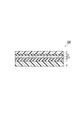
- FIG. 1 is a schematic cross-sectional view of a transparent gas barrier laminated film according to the first embodiment of the present invention.
- the transparent gas barrier laminated film 100 of the present embodiment is a first transparent film in which a gas barrier layer 6 is formed on a second transparent plastic film substrate 2 via a first adhesive layer 7a.
- the plastic film substrate 1 and the sealing layer 8 are arranged in this order.
- the first transparent plastic film base material on which the gas barrier layer is formed and the sealing layer are provided on the second transparent plastic film base material 2 via the first adhesive layer 7a. Because it is a laminated film arranged sequentially, it can be applied to uneven printed boards without wrinkles, and it can be heat-sealed as a sealing layer as a close-contact layer, and a transparent gas barrier laminate with excellent gas barrier properties A film is obtained.
- a substrate having a total light transmittance of 85% or more is desirable, but any plastic film that can be used as a normal optical material can be used without particular limitation.
- plastic films include polyolefins such as homopolymers or copolymers such as ethylene, propylene, and butene, polyesters such as polyethylene terephthalate and polyethylene naphthalate, nylon 6, nylon 66, nylon 12, and copolymer nylon.
- polyamide, polycarbonate and the like polyethylene terephthalate, polyethylene naphthalate, or the like can be suitably used as a substrate having high transparency and excellent heat resistance.
- the thickness of the first transparent plastic film substrate 1 is not particularly limited, but is desirably 50 ⁇ m or less in order to reduce the total thickness of the transparent gas barrier laminated film 100.
- the thickness of the first transparent plastic film substrate 1 is desirably 12 ⁇ m or more in order to form the gas barrier layer 6 and obtain excellent gas barrier properties.
- the gas barrier layer 6 preferably includes the inorganic thin film layer 4 and the gas barrier coating layer 5. As shown in FIG. 1, the gas barrier layer 6 includes an inorganic thin film layer 4 formed on one surface of the first transparent plastic film substrate 1, and the gas barrier coating layer 5 is formed on the inorganic thin film layer 4. Are stacked.
- the inorganic thin film layer 4 is not particularly limited, and for example, an inorganic oxide thin film such as aluminum oxide, silicon oxide, magnesium oxide, or a mixture thereof can be used. Among these, it is desirable to use aluminum oxide or silicon oxide from the viewpoint of barrier properties and productivity.
- the thickness (film thickness) of the inorganic thin film layer 4 is preferably in the range of 5 to 500 nm, more preferably in the range of 10 to 100 nm.
- the film thickness is 5 nm or more, it is easy to form a uniform film, and the function as a gas barrier material tends to be more sufficiently achieved.
- the film thickness is 500 nm or less, sufficient flexibility can be maintained by the thin film (gas barrier layer), and cracks occur in the thin film (gas barrier layer) due to external factors such as bending and pulling after film formation. There is a tendency to prevent this more reliably.
- a normal vacuum vapor deposition method can be used as a method of forming a vapor deposition layer made of an inorganic oxide on the first transparent plastic film substrate 1 as the inorganic thin film layer 4.
- other thin film forming methods such as sputtering, ion plating, and plasma vapor deposition (CVD) can also be used.
- the vacuum evaporation method can be used preferably.
- a heating means of the vacuum evaporation method any of an electron beam heating method, a resistance heating method, and an induction heating method is preferable.
- vapor-deposit in order to improve the adhesiveness of a vapor deposition layer and a base material, and the denseness of a vapor deposition layer, it is also possible to vapor-deposit using a plasma assist method or an ion beam assist method.
- reactive vapor deposition in which oxygen gas or the like is blown can be performed.
- the gas barrier coating layer 5 is provided in order to prevent various secondary damages in the subsequent process and to impart high barrier properties.
- This gas barrier coating layer 5 contains, as a component, at least one selected from the group consisting of a hydroxyl group-containing polymer compound, a metal alkoxide, a metal alkoxide hydrolyzate, and a metal alkoxide polymer from the viewpoint of obtaining excellent barrier properties. It is preferable.
- hydroxyl group-containing polymer compound examples include water-soluble polymers such as polyvinyl alcohol, polyvinyl pyrrolidone, and starch, and the barrier property is most excellent particularly when polyvinyl alcohol is used.
- the metal alkoxide is represented by the general formula: M (OR) n (M represents a metal atom such as Si, Ti, Al, Zr, R represents an alkyl group such as —CH 3 , —C 2 H 5 , and n represents M Represents an integer corresponding to the valence of.
- M represents a metal atom such as Si, Ti, Al, Zr
- R represents an alkyl group such as —CH 3 , —C 2 H 5
- n represents M Represents an integer corresponding to the valence of.
- Specific examples include tetraethoxysilane [Si (OC 2 H 5 ) 4 ], triisopropoxyaluminum [Al (O-iso-C 3 H 7 ) 3 ] and the like. Tetraethoxysilane and triisopropoxyaluminum are preferable because they are relatively stable in an aqueous solvent after hydrolysis.
- hydrolyzate and polymer of metal alkoxide include, for example, silicic acid (Si (OH) 4 ) as a hydrolyzate or polymer of tetraethoxysilane, and a hydrolyzate or polymer of tripropoxyaluminum.
- silicic acid Si (OH) 4
- examples of the hydrolyzate and polymer of metal alkoxide include, for example, silicic acid (Si (OH) 4 ) as a hydrolyzate or polymer of tetraethoxysilane, and a hydrolyzate or polymer of tripropoxyaluminum.
- Al (OH) 3 aluminum hydroxide
- the thickness (film thickness) of the gas barrier coating layer 5 is preferably in the range of 50 to 1000 nm, and more preferably in the range of 100 to 500 nm.
- the film thickness is 50 nm or more, there is a tendency that sufficient gas barrier properties can be obtained, and when it is 1000 nm or less, there is a tendency that sufficient flexibility can be maintained by the thin film (gas barrier layer).
- Conventionally known means such as a commonly used dipping method, roll coating method, screen printing method, spraying method, and gravure printing method can be used for the coating method of the coating agent containing the material that becomes the gas barrier coating layer.
- the second transparent plastic film substrate 2 a plastic film similar to the first transparent plastic film substrate 1 can be used.
- the gas barrier layer 6 is protected and printed. Wrinkles due to unevenness on the printed circuit board when bonded to the substrate can be suppressed.
- the shrinkage rate when the second transparent plastic film substrate 2 is heated at 150 ° C. for 30 minutes is 5% or more and 15 % Or less is desirable.
- the thermal shrinkage rate of the second transparent plastic film base material 5% or more when laminating and sealing the electronic paper substrate, the transparent gas barrier laminated film is deformed along the uneven printed substrate, It tends to be easier to apply without wrinkles. If the thermal contraction rate is 15% or less, there is a tendency that it is easier to maintain the barrier property without damaging the gas barrier layer 6 even when the transparent gas barrier laminated film is deformed by heat.
- the thermal contraction rate of the second transparent plastic film substrate 2 can be measured according to the measurement method of JIS K 7133.
- the second transparent plastic film substrate has different heat shrinkage rates in the TD direction (Transverse direction) and the MD direction (Machine direction)
- at least the larger one of the heat shrinkage rates in the TD direction and the MD direction is larger. It may be within the above range. Since the larger one of the thermal shrinkage rates in at least the TD direction and the MD direction is within the above range, the second transparent plastic film base material 2 shrinks and deforms due to heating during lamination, resulting in unevenness on the printed circuit board. It is possible to follow and further suppress the generation of wrinkles due to unevenness.
- a polyolefin resin film such as a polypropylene film is particularly preferable.
- a polypropylene film as the second transparent plastic film substrate, it is possible to follow the irregularities on the printed circuit board when bonded to the printed circuit board, and to further suppress wrinkles due to the irregularities.
- the second transparent plastic film substrate 2 contains an ultraviolet absorber or a fluorescent whitening agent.
- an ultraviolet absorber or a fluorescent brightening agent By adding an ultraviolet absorber or a fluorescent brightening agent to the second transparent plastic film substrate 2, a function of suppressing ultraviolet transmission can be imparted. Examples of the method of adding the ultraviolet absorber or the fluorescent brightening agent to the second transparent plastic film substrate 2 include impregnation.
- the thickness of the second transparent plastic film substrate 2 is not particularly limited, but is desirably 100 ⁇ m or less in order to reduce the total thickness of the transparent gas barrier laminated film 100.
- the thickness of the second transparent plastic film substrate 2 can be, for example, 12 ⁇ m or more, and can be 25 ⁇ m or more, from the viewpoint of easily suppressing wrinkles caused by unevenness on the printed circuit board. 30 ⁇ m or more.
- the first adhesive layer 7 a is provided for bonding the second transparent plastic film substrate 2 and the gas barrier layer 6 formed on the first transparent plastic film substrate 1. It has been. Although it does not specifically limit as the 1st contact bonding layer 7a, Adhesives or adhesives, such as an acryl-type material, a urethane type material, and a polyester-type material, can be used. More specifically, any of an acrylic pressure-sensitive adhesive, an acrylic adhesive, a urethane adhesive, and an ester adhesive can be used. In particular, the pressure-sensitive adhesive is excellent in conformity to the unevenness of the printed board when the transparent gas barrier laminated film is laminated and bonded onto the printed board for electronic paper. Furthermore, an acrylic pressure-sensitive adhesive is suitable because it is excellent in transparency.
- the first adhesive layer 7a preferably contains an ultraviolet absorber or a fluorescent brightening agent. Also in the electronic paper element, it is preferable that the transparent gas barrier laminated film has a function of suppressing ultraviolet light transmission in order to protect internal components such as liquid crystal. By adding an ultraviolet absorber or fluorescent brightening agent to the first adhesive layer 7a, a function of suppressing ultraviolet transmission can be imparted.
- the thickness of the first adhesive layer 7a is not particularly limited, but is desirably 30 ⁇ m or less in order to reduce the total thickness of the transparent gas barrier laminated film 100. On the other hand, from the viewpoint of obtaining better adhesiveness, the thickness of the first adhesive layer 7a is desirably 3 ⁇ m or more.
- the adhesive layer can be formed by applying an adhesive to any of the surfaces to be bonded and drying if necessary.
- a reverse roll coater knife coater, bar coater, slot die coater, air knife coater, reverse gravure coater, vario gravure coater or the like is used.
- the application amount of the pressure-sensitive adhesive is desirably in the range of 1 to 30 ⁇ m in thickness.
- the seal layer 8 is formed on the other surface of the first transparent plastic film substrate.
- the material of the sealing layer 8 include polyethylene, polypropylene, ethylene / vinyl acetate copolymer, ethylene / methacrylic acid copolymer, ethylene / methacrylic acid ester copolymer, ethylene / acrylic acid copolymer, and ethylene / acrylic acid.
- resins such as ester copolymers and cross-linked products of these can be used, it is desirable to use ethylene / vinyl acetate copolymer resins from the viewpoint of processability and flexibility.
- the sealing layer 8 contains an ethylene / vinyl acetate copolymer resin, when the electronic paper is sealed, deformation of the transparent gas barrier laminated film can be suppressed, and damage to the barrier layer can be reduced.
- the vinyl acetate content is preferably 10 to 30 mol%. That is, the content of structural units derived from vinyl acetate in all structural units of the ethylene / vinyl acetate copolymer resin is preferably 10 to 30 mol%.
- the vinyl acetate content is 10 mol% or more, the low-temperature sealing property is excellent, and the electronic paper is more easily sealed.
- the transparent gas barrier laminated film of the present embodiment by heat-sealing the sealing layer to the printed board, it can be attached to an uneven printed board without wrinkles, and an electronic paper element having excellent sealing strength can be obtained.
- a transparent gas barrier laminate film is arranged on a printed circuit board having unevenness due to a circuit or the like so that the unevenness and the seal layer face each other, and the printed circuit board and the transparent gas barrier adhesive film are heated and pressurized (heated).
- the printed circuit board and the transparent gas barrier adhesive film are heated and pressurized (heated).
- the thickness of the seal layer 8 is determined according to the purpose, but is generally in the range of 15 to 200 ⁇ m.
- an anchor coat layer (not shown) can be used in order to further improve the adhesion. That is, the anchor coat layer is provided between the first transparent plastic film substrate 1 and the seal layer 8.
- an anchor coat layer is not specifically limited, Adhesives or adhesives, such as an acryl-type material, a urethane type material, and a polyester-type material, can be used.
- an extrusion lamination method or the like can be preferably used, but other known methods can also be used for lamination.
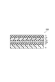
- FIG. 2 is a schematic cross-sectional view of a transparent gas barrier laminated film 200 according to the second embodiment of the present invention.
- the transparent gas barrier laminate film 200 of the second embodiment is simply the number of the third transparent plastic film substrate 3 and the second adhesive layer 7b increased from the transparent gas barrier laminate film 100 of the first embodiment. Therefore, about the transparent gas barrier laminated film 200 of 2nd Embodiment, while attaching
- the transparent gas barrier laminated film 200 of the present embodiment has a third transparent plastic film substrate 3 on the second transparent plastic film substrate 2 via a second adhesive layer 7b.
- the structure is arranged.
- the third transparent plastic film substrate 3 the same material as that of the first transparent plastic film substrate 1 can be used.
- the third transparent plastic film substrate 3 includes a polyethylene terephthalate film and a polyethylene naphthalate.
- a polyester film such as a film
- the third transparent plastic film substrate has a thermal shrinkage rate of 5% or less at 150 ° C. for 30 minutes.
- the same material as that of the first adhesive layer 7a can be used, but an ultraviolet absorber or a fluorescent brightener is added to the third transparent plastic film substrate 3.
- an ultraviolet absorber or a fluorescent brightener is added to the third transparent plastic film substrate 3.
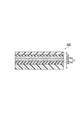
- FIG. 3 is a schematic cross-sectional view of a transparent gas barrier laminate film according to a third embodiment of the present invention.
- the transparent gas barrier laminated film 300 of the third embodiment is a second transparent instead of containing either an ultraviolet absorber or a fluorescent brightening agent in the first adhesive layer 7a of the transparent gas barrier laminated film 100 of the first embodiment.
- a coating layer 9 containing one or more of an ultraviolet absorber and a fluorescent brightening agent is provided under the plastic film substrate 2 (on the gas barrier layer side).
- This coat layer 9 Since the coat layer 9 has a function of suppressing ultraviolet light transmission, the coat layer 9 is provided in order to maintain the display performance of the electronic paper satisfactorily over a long period of time.
- This coat layer 9 is made of benzophenone, benzotriazole, hydroxyphenyltriazine, benzoxazolylthiophene and distyryl, which are UV absorbers or fluorescent brighteners, from the viewpoint of obtaining an excellent UV transmission suppressing function and high transparency. It is preferable that at least one selected from the group consisting of biphenyl derivatives is contained as a component.
- the coating layer 9 is formed by applying a coating agent containing an ultraviolet absorber or a fluorescent brightening agent on one surface of the second transparent plastic film substrate 2 and drying the dried coating surface and the first transparent plastic film.
- the gas barrier layer 6 formed on the substrate 1 is opposed to the first transparent plastic film substrate 2 and the first transparent plastic film substrate 2 by bonding them with an adhesive or pressure-sensitive adhesive that becomes the first adhesive layer 7a. Between the adhesive layer 7a.
- Conventionally known means such as a commonly used dipping method, roll coating method, screen printing method, spray method, and gravure printing method can be used for the coating method of the coating agent containing an ultraviolet absorber or a fluorescent brightening agent.
- the thickness of the coating layer varies depending on the type of coating agent, the processing machine and the processing conditions, but is preferably in the range of 0.01 to 50 ⁇ m, more preferably in the range of 1 to 30 ⁇ m.
- FIG. 4 is a schematic cross-sectional view of a transparent gas barrier laminate film 400 according to the fourth embodiment of the present invention.
- the gas barrier layer 6 of the transparent gas barrier laminate film 100 of the first embodiment has a two-layer configuration in which the inorganic thin film layers 4 and the gas barrier coating layers 5 are alternately laminated.
- the gas barrier layer 6 of the transparent gas barrier laminated film 400 includes the first gas barrier layer 6a composed of the first inorganic thin film layer 4a and the first gas barrier coating layer 5a, the second inorganic thin film layer 4b, and the second gas barrier coating.
- the second gas barrier layer 6b composed of the layer 5b has a two-layer structure (first gas barrier layer 6a and second gas barrier layer 6b) formed in this order, and the gas barrier layer 6 is a first transparent plastic. It is formed on the film substrate 1. Thereby, the gas barrier property of a transparent gas barrier laminated film can further be improved.
- the gas barrier layer 6 is not limited to two layers, but may have a multilayer structure of three or more layers.
- the gas barrier layer 6 is formed only on one side of the 1st transparent plastic film base material 1, both surfaces (one side and the other side) of the 1st transparent plastic film base material 1 It may be formed on the surface.
- the inorganic thin film layer 4 is also formed on the other surface of the first transparent plastic film substrate 1, and the gas barrier coating layer 5 is laminated on the inorganic thin film layer 4.
- the sealing layer 8 is formed on the other surface (surface on the opposite side to the 2nd transparent plastic film base material 2) of the 1st transparent plastic film base material 1, It may be formed on the other surface of the transparent plastic film substrate 2 (the surface opposite to the first transparent plastic film substrate 1).
- the seal layer 8 may be formed on the other surface of the second transparent plastic film substrate 2, It may be formed on the other surface of the first transparent plastic film substrate 1 via a gas barrier layer. Therefore, in one embodiment of the transparent gas barrier laminate film of the present invention, the gas barrier layer 6 may be sandwiched between the first transparent plastic film substrate 1 and the seal layer 8.
- the third transparent plastic film substrate 3 is connected to the first adhesive layer 7b via the first adhesive layer 7b. It is arranged (formed) on the other surface of the transparent plastic film substrate 1.
- an anchor coat layer made of polyurethane resin is applied to the surface of the first transparent plastic film substrate opposite to the gas barrier layer by a wet coating method, an ethylene / vinyl acetate copolymer resin is applied on the coated surface. Then, a sealing layer made of an ethylene / vinyl acetate copolymer resin was formed on the other surface of the first transparent plastic film substrate via an anchor coat layer. Thereby, the transparent gas barrier laminated film of the structure 1 based on 1st Embodiment shown in FIG. 1 was produced.
- the printed circuit board was brought into close contact with the seal layer of the obtained transparent gas barrier laminated film, and heat-sealed and pasted to produce an electronic paper element having configuration 1.
- the second transparent plastic film substrate as a second transparent plastic film having a thickness of 50 ⁇ m (OPP, thermal shrinkage rate in the TD direction (maximum shrinkage direction) at 150 ° C. for 30 minutes: 9.2%)
- OPP thermal shrinkage rate in the TD direction (maximum shrinkage direction) at 150 ° C. for 30 minutes: 9.2%
- a pressure-sensitive adhesive made of an acrylic resin to which a 3% by weight UV absorber is added with respect to the solid content of the acrylic resin is applied by a wet coating method, and the second transparent is applied through the applied pressure-sensitive adhesive.
- a plastic film substrate and a 12 ⁇ m thick polyethylene terephthalate film (PET) as a third transparent plastic film substrate were bonded together.
- the other surface of the second transparent plastic film substrate bonded to the third transparent plastic film substrate as described above is made of an acrylic resin to which no ultraviolet absorber is added as the first adhesive layer.
- the pressure-sensitive adhesive was applied by the wet coating method, and the second transparent plastic film substrate and the gas barrier layer formed on the first transparent plastic film substrate were bonded to each other through the applied pressure-sensitive adhesive. .
- an anchor coat layer and a seal layer are formed on the surface opposite to the gas barrier layer of the first transparent plastic film substrate by the same operation as in the first configuration, and the second embodiment shown in FIG.
- the transparent gas barrier laminated film of the structure 2 based on this was produced.
- the electronic paper element of the structure 2 was obtained by operation similar to the structure 1 except having used this transparent gas barrier laminated film.
- silicon oxide is provided as an inorganic thin film layer to a thickness of 250 mm by vacuum deposition, and tetraethoxysilane and polyvinyl alcohol are formed on the inorganic thin film layer.
- tetraethoxysilane and polyvinyl alcohol are formed on the inorganic thin film layer.
- a wet coating method to form a gas barrier coating layer having a thickness of 0.3 ⁇ m.
- silicon oxide is provided as an inorganic thin film layer with a thickness of 250 mm, and a coating liquid containing tetraethoxysilane and polyvinyl alcohol is applied on the inorganic thin film layer by a wet coating method.
- a gas barrier coating layer having a thickness of 3 ⁇ m was formed.
- the configuration according to the fourth embodiment shown in FIG. 4 is the same as the configuration 1 except that the gas barrier layer is formed by alternately laminating the inorganic thin film layer and the gas barrier coating layer. 3 transparent gas barrier laminated films were obtained. Furthermore, the electronic paper element of the structure 3 was obtained by operation similar to the structure 1 except having used this transparent gas barrier laminated film.
- a transparent gas barrier laminate film of Configuration 5 was obtained in the same manner as in Configuration 1 except that an adhesive made of an acrylic resin without adding an ultraviolet absorber was used. Furthermore, the electronic paper element of the structure 5 was obtained by operation similar to the structure 1 except having used this transparent gas barrier laminated film.
- Comparative example> [Comparison configuration 1]
- the transparent structure of Comparative Structure 1 was prepared in the same manner as in Structure 1, except that a 12 ⁇ m-thick polyvinylidene chloride (PVDC) -coated polyethylene terephthalate film was used instead of the gas barrier layer comprising the inorganic thin film layer and the gas barrier coating layer.
- PVDC polyvinylidene chloride
- a gas barrier laminated film was obtained.
- the electronic paper element of the comparative structure 1 which is a comparative example was obtained by the same operation as the structure 1 except having used this transparent gas barrier laminated film.
- Table 1 summarizes the production conditions and evaluation results of the configurations 1 to 5 of the example and the comparative configuration 1 of the comparative example.
- the transparent gas barrier laminated films having constitutions 1 to 5 showed good barrier properties by having an inorganic thin film layer, a gas barrier coating layer, and a seal layer.
- configurations 1 to 4 since the ultraviolet absorber is added to the first adhesive layer or the adhesive of the second adhesive layer, it has a function of suppressing ultraviolet transmission.
- configurations 1 to 3 a polypropylene film is used for the second transparent plastic film substrate or the third transparent plastic film substrate, so that even if there are irregularities on the printed circuit board, it is applied without wrinkles. It was possible to attach an electronic paper element having a good appearance.
- the configurations 1 to 3 and 5 in which the polypropylene film is used have fewer wrinkles in appearance. Met. However, since the wrinkles seen in the configuration 4 were not conspicuous, it was judged that there was no problem in appearance.
- the ultraviolet transmittance is high, and there is a possibility that stable display performance of the electronic paper element cannot be expected.
- the second transparent plastic film substrate and the gas barrier layer formed on the first transparent plastic film substrate were bonded through the coated adhesive and the coated adhesive.
- an anchor coat layer made of polyurethane resin is applied to the surface of the first transparent plastic film substrate opposite to the gas barrier layer by a wet coating method, and the vinyl acetate content is 20 mol on the coated surface.
- the electronic paper element of the structure 6 was produced in the same operation as the structure 1 except having used said transparent gas barrier laminated film.
- the third operation shown in FIG. 3 was carried out in the same manner as in the configuration 6 except that the coating layer was applied and an adhesive made of an acrylic resin to which no UV absorber was added was applied on the coating layer.
- a transparent gas barrier laminated film of configuration 7 was obtained.
- the electronic paper element of the structure 7 was obtained by the same operation as the structure 6 except having used this transparent gas barrier laminated film.
- silicon oxide is provided as an inorganic thin film layer to a thickness of 250 mm by vacuum deposition, and tetraethoxysilane and polyvinyl alcohol are formed on the inorganic thin film layer.
- tetraethoxysilane and polyvinyl alcohol are formed on the inorganic thin film layer.
- a wet coating method to form a gas barrier coating layer having a thickness of 0.3 ⁇ m.
- silicon oxide is provided as an inorganic thin film layer with a thickness of 250 mm, and a coating liquid containing tetraethoxysilane and polyvinyl alcohol is applied on the inorganic thin film layer by a wet coating method.
- a gas barrier coating layer having a thickness of 3 ⁇ m was formed.
- the configuration according to the fourth embodiment shown in FIG. 4 is the same as the configuration 6 except that the gas barrier layer is formed by alternately laminating the inorganic thin film layer and the gas barrier coating layer two layers as described above. 9 transparent gas barrier laminated films were obtained. Furthermore, the electronic paper element of the structure 9 was obtained by operation similar to the structure 6 except having used this transparent gas barrier laminated film.
- Configuration 10 A transparent gas barrier laminate film of Configuration 10 was obtained in the same manner as in Configuration 6, except that an adhesive made of an acrylic resin without adding an ultraviolet absorber was used. Furthermore, the electronic paper element of the structure 10 was obtained by operation similar to the structure 6 except having used this transparent gas barrier laminated film.
- Configuration 11 A transparent gas barrier laminate film of Configuration 11 was obtained in the same manner as in Configuration 6, except that an ethylene / vinyl acetate copolymer resin having a vinyl acetate content of 7% was used as the seal layer. Furthermore, the electronic paper element of the structure 11 was obtained by operation similar to the structure 6 except having used this transparent gas barrier laminated film.
- the transparent gas barrier laminated film produced in configurations 6 to 11 and the electronic paper element were evaluated as follows.
- the transparent gas barrier laminate film and electronic paper element produced in configurations 6 to 11 were measured under the same conditions as the transparent gas barrier laminate film and electronic paper element produced in configurations 1 to 5 and comparative configuration 1 except for the following measurements. It was.
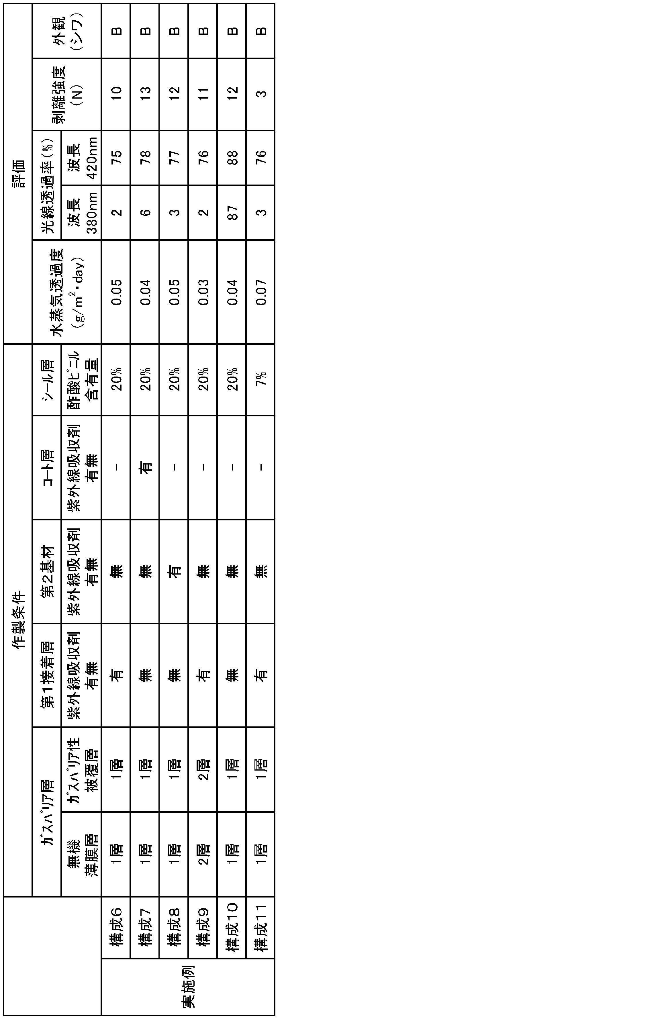
- Table 2 summarizes the fabrication conditions and evaluation results for configurations 6-11.
- the transparent gas barrier laminated films having constitutions 6 to 11 showed good barrier properties by having an inorganic thin film layer, a gas barrier coating layer, and a seal layer.
- the transparent gas barrier laminated films having configurations 6 to 9 and 11 have a function of suppressing ultraviolet transmission because the ultraviolet absorber is added to the first adhesive layer, the coat layer, or the second transparent plastic film substrate. It was.
- the sealing layer is formed by extrusion lamination of ethylene / vinyl acetate copolymer resin having a vinyl acetate content of 20%, and the obtained transparent gas barrier laminated film is used to heat seal the printed circuit board. Since the electronic paper element was produced, it was able to be affixed to the printed circuit board with sufficient sealing strength (adhesion).
- the ultraviolet absorber since the ultraviolet absorber is not added, the ultraviolet transmittance is high, and there is a possibility that stable display performance of the electronic paper element cannot be expected.
- the transparent gas barrier laminate film of the present invention is a display such as an electronic paper element and an organic EL element based on a plastic film that requires a high gas barrier property or UV resistance, a flexible packaging material, and an industrial material application such as a solar cell. It can be applied to.
- SYMBOLS 1 ... 1st transparent plastic film base material, 2 ... 2nd transparent plastic film base material, 3 ... 3rd transparent plastic film base material, 4 ... Inorganic thin film layer, 5 ... Gas barrier coating layer, 6 ... Gas barrier layer 7a ... first adhesive layer, 7b ... second adhesive layer, 8 ... seal layer, 9 ... coat layer, 100, 200, 300, 400 ... transparent gas barrier laminated film.
Landscapes
- Chemical & Material Sciences (AREA)
- Chemical Kinetics & Catalysis (AREA)
- Organic Chemistry (AREA)
- Physics & Mathematics (AREA)
- Health & Medical Sciences (AREA)
- Medicinal Chemistry (AREA)
- Polymers & Plastics (AREA)
- Engineering & Computer Science (AREA)
- Nonlinear Science (AREA)
- Optics & Photonics (AREA)
- Materials Engineering (AREA)
- Mechanical Engineering (AREA)
- Metallurgy (AREA)
- Inorganic Chemistry (AREA)
- Crystallography & Structural Chemistry (AREA)
- General Physics & Mathematics (AREA)
- Mathematical Physics (AREA)
- Ceramic Engineering (AREA)
- Laminated Bodies (AREA)
Abstract
Description
まず、本発明の第1実施形態について説明する。図1は、本発明の第1実施形態に係る透明ガスバリア積層フィルムの模式断面図である。
次に、本発明の第2実施形態について説明する。図2は、本発明の第2実施形態に係る透明ガスバリア積層フィルム200の模式断面図である。第2実施形態の透明ガスバリア積層フィルム200は、第1実施形態の透明ガスバリア積層フィルム100から、第3の透明プラスチックフィルム基材3、及び第2の接着層7bが増えただけである。従って、第2実施形態の透明ガスバリア積層フィルム200については、第1実施形態と同一の構成部分については同じ符号を付すると共に説明を省略する。
次に、本発明の第3実施形態について説明する。図3は、本発明の第3実施形態に係る透明ガスバリア積層フィルムの模式断面図である。第3実施形態の透明ガスバリア積層フィルム300は、第1実施形態の透明ガスバリア積層フィルム100の第1の接着層7aに紫外線吸収剤又は蛍光増白剤をいずれも含まない代わりに、第2の透明プラスチックフィルム基材2の下(ガスバリア層側)に、紫外線吸収剤又は蛍光増白剤のいずれか1種以上を含むコート層9を設けた構成となっている。
次に、本発明の第4実施形態について説明する。図4は、本発明の第4実施形態に係る透明ガスバリア積層フィルム400の模式断面図である。第4実施形態の透明ガスバリア積層フィルム400では、第1実施形態の透明ガスバリア積層フィルム100のガスバリア層6が、無機薄膜層4とガスバリア性被覆層5とが交互に積層した2層構成となっている。言い換えると、透明ガスバリア積層フィルム400のガスバリア層6は、第1無機薄膜層4aと第1ガスバリア性被覆層5aとからなる第1ガスバリア層6aと、第2無機薄膜層4bと第2ガスバリア性被覆層5bとからなる第2ガスバリア層6bとが、この順で形成された2層(第1ガスバリア層6aと第2ガスバリア層6b)構成となっており、このガスバリア層6が第1の透明プラスチックフィルム基材1上に形成されている。これにより、透明ガスバリア積層フィルムのガスバリア性をさらに高めることができる。なお、本実施形態では、ガスバリア層6を2層に限らず3層以上の多層構成とすることができる。
[構成1]
(ガスバリア層の形成)
第1の透明プラスチックフィルム基材としての厚み12μmのポリエチレンテレフタレートフィルムの片面に、無機薄膜層として酸化珪素を真空蒸着法により250Åの厚みに設けた。さらに、テトラエトキシシランとポリビニルアルコールとを含む塗液をウェットコーティング法により無機薄膜層上に塗工し、0.3μmの厚みのガスバリア性被覆層を形成した。これにより、第1の透明プラスチックフィルム基材の一方の面上に無機薄膜層及びガスバリア性被覆層からなるガスバリア層を形成した。
続いて、第2の透明プラスチックフィルム基材としての厚み50μmのポリプロピレンフィルム(OPP、150℃30分でのTD方向(最大収縮方向)の熱収縮率:9.2%)の片面に、アクリル樹脂の固形分に対し3%重量比分の紫外線吸収剤を添加したアクリル樹脂からなる粘着剤をウェットコーティング法により塗工した。塗工した粘着剤を介して、第2の透明プラスチックフィルム基材と第1の透明プラスチックフィルム基材上に形成されたガスバリア層面との貼り合わせを行った。
得られた透明ガスバリア積層フィルムのシール層にプリント基板を密着させ、ヒートシールを行い貼り付けることで、構成1の電子ペーパー素子を作製した。
まず、構成1と同様の操作にて、第1の透明プラスチックフィルム基材の一方の面上に無機薄膜層及びガスバリア性被覆層からなるガスバリア層を形成した。
第1の透明プラスチックフィルム基材としての厚み12μmのポリエチレンテレフタレートフィルムの片面に、無機薄膜層として酸化珪素を真空蒸着法により250Åの厚みに設け、その無機薄膜層上に、テトラエトキシシランとポリビニルアルコールとを含む塗液をウェットコーティング法により塗工し、0.3μmの厚みのガスバリア性被覆層を形成した。さらにガスバリア性被覆層の上に、無機薄膜層として酸化珪素を250Åの厚みに設け、その無機薄膜層上に、テトラエトキシシランとポリビニルアルコールとを含む塗液をウェットコーティング法により塗工し、0.3μmの厚みのガスバリア性被覆層を形成した。これにより、無機薄膜層とガスバリア性被覆層が交互に2層ずつ積層されたガスバリア層としたこと以外は、構成1と同様の操作にて、図4に示した第4実施形態に係る、構成3の透明ガスバリア積層フィルムを得た。さらに、この透明ガスバリア積層フィルムを用いたこと以外は、構成1と同様の操作にて、構成3の電子ペーパー素子を得た。
第2の透明プラスチックフィルム基材として、厚み50μmのポリプロピレンフィルムの代わりに、厚み25μmのポリエチレンテレフタレートフィルム(PET、150℃30分でのTD方向(最大収縮方向)の熱収縮率:1.0%以下)を用いたこと以外は、構成1と同様の操作にて、構成4の透明ガスバリア積層フィルムを得た。さらに、この透明ガスバリア積層フィルムを用いたこと以外は、構成1と同様の操作にて、構成4の電子ペーパー素子を得た。
紫外線吸収剤を添加しないアクリル樹脂からなる粘着剤を用いたこと以外は、構成1と同様の操作にて、構成5の透明ガスバリア積層フィルムを得た。さらに、この透明ガスバリア積層フィルムを用いたこと以外は、構成1と同様の操作にて、構成5の電子ペーパー素子を得た。
[比較構成1]
無機薄膜層とガスバリア性被覆層からなるガスバリア層の代わりに、厚み12μmのポリ塩化ビニリデン(PVDC)コートポリエチレンテレフタレートフィルムを用いたこと以外は、構成1と同様の操作にて、比較構成1の透明ガスバリア積層フィルムを得た。さらに、この透明ガスバリア積層フィルムを用いたこと以外は、構成1と同様の操作にて、比較例である比較構成1の電子ペーパー素子を得た。
実施例の構成1~5、及び比較例の比較構成1で作製した透明ガスバリア積層フィルムについて、水蒸気透過率測定装置(モダンコントロール社製 PERMATRAN 3/31)を使用して、水蒸気透過度を、温度40℃、湿度90%RHの条件下で測定した。
実施例の構成1~5、及び比較例の比較構成1で作製した透明ガスバリア積層フィルムについて、分光光度計(島津製作所社製 UV-3100)を使用して、波長400nmでの光線透過率を測定した。
実施例の構成1~5、及び比較例の比較構成1で作製した電子ペーパー素子について、プリント基板に貼り付けられた透明ガスバリア積層フィルムの外観を目視にて確認した。シワがなく外観良好なものを「A」、一部シワが見られるが目立たないものを「B」、不良となるような多数のシワがあるものを「C」と判定した。

(ガスバリア層の形成)
まず、構成1と同様の操作にて、第1の透明プラスチックフィルム基材の一方の面上に無機薄膜層及びガスバリア性被覆層からなるガスバリア層を形成した。
続いて、第2の透明プラスチックフィルム基材としての厚み12μmのポリエチレンテレフタレートフィルムの片面に、アクリル樹脂の固形分に対し3%重量比分の紫外線吸収剤を添加したアクリル樹脂からなる粘着剤をウェットコーティング法により塗工し、塗工した粘着剤を介して、第2の透明プラスチックフィルム基材と第1の透明プラスチックフィルム基材上に形成されたガスバリア層との貼り合わせを行った。
上記の透明ガスバリア積層フィルムを用いたこと以外は、構成1と同様の操作にて、構成6の電子ペーパー素子を作製した。
第2の透明プラスチックフィルム基材としての厚み12μmのポリエチレンテレフタレートフィルムの片面に、ポリエステル樹脂の固形分に対し5%重量比分の紫外線吸収剤を添加したポリエステル樹脂からなるコーティング剤をウェットコーティング法により塗工しコート層を設けたこと、さらに紫外線吸収剤を添加しないアクリル樹脂からなる粘着剤をコート層上に塗工したこと以外は、構成6と同様の操作にて、図3に示した第3実施形態に係る、構成7の透明ガスバリア積層フィルムを得た。さらに、この透明ガスバリア積層フィルムを用いたこと以外は、構成6と同様の操作にて、構成7の電子ペーパー素子を得た。
第2の透明プラスチックフィルム基材として、染色法により紫外線吸収剤を含浸させた厚み12μmのポリエチレンテレフタレートフィルムを使用したこと、さらに紫外線吸収剤を添加しないアクリル樹脂からなる粘着剤を用いたこと以外は、構成6と同様の操作にて、図1に示した第1実施形態に係る、構成8の透明ガスバリア積層フィルムを得た。さらに、この透明ガスバリア積層フィルムを用いたこと以外は、構成6と同様の操作にて、構成8の電子ペーパー素子を得た。
第1の透明プラスチックフィルム基材としての厚み12μmのポリエチレンテレフタレートフィルムの片面に、無機薄膜層として酸化珪素を真空蒸着法により250Åの厚みに設け、その無機薄膜層上に、テトラエトキシシランとポリビニルアルコールとを含む塗液をウェットコーティング法により塗工し0.3μmの厚みのガスバリア性被覆層を形成した。さらにそのガスバリア性被覆層の上に、無機薄膜層として酸化珪素を250Åの厚みに設け、その無機薄膜層上に、テトラエトキシシランとポリビニルアルコールとを含む塗液をウェットコーティング法により塗工し0.3μmの厚みのガスバリア性被覆層を形成した。上記のとおり無機薄膜層とガスバリア性被覆層が交互に2層ずつ積層されたガスバリア層としたこと以外は、構成6と同様の操作にて、図4に示した第4実施形態に係る、構成9の透明ガスバリア積層フィルムを得た。さらに、この透明ガスバリア積層フィルムを用いたこと以外は、構成6と同様の操作にて、構成9の電子ペーパー素子を得た。
紫外線吸収剤を添加しないアクリル樹脂からなる粘着剤を用いたこと以外は、構成6と同様の操作にて、構成10の透明ガスバリア積層フィルムを得た。さらに、この透明ガスバリア積層フィルムを用いたこと以外は、構成6と同様の操作にて、構成10の電子ペーパー素子を得た。
シール層として、酢酸ビニル含有量が7%である、エチレン・酢酸ビニル共重合樹脂を用いたこと以外は、構成6と同様の操作にて、構成11の透明ガスバリア積層フィルムを得た。さらに、この透明ガスバリア積層フィルムを用いたこと以外は、構成6と同様の操作にて、構成11の電子ペーパー素子を得た。
構成6~11で作製した透明ガスバリア積層フィルムについて、分光光度計(島津製作所社製 UV-3100)を使用して、波長380nm及び420nmでの光線透過率を測定した。
構成6~11で作製した電子ペーパー素子について、透明ガスバリア積層フィルムとプリント基板とのシール強度評価として、剥離試験機(島津製作所社製 AGS-X)を使用して、試験片15mm幅、剥離角度180度、剥離速度300mm/minにて、剥離強度を測定した。
Claims (15)
- 少なくとも一方の面に無機薄膜層を含むガスバリア層が形成された第1の透明プラスチックフィルム基材の前記ガスバリア層が形成された面と、第2の透明プラスチックフィルム基材の一方の面とが、第1の接着層を介して貼り合わされ、
前記第1の透明プラスチックフィルム基材又は前記第2の透明プラスチックフィルム基材の他方の面にシール層が形成された、透明ガスバリア積層フィルム。 - 前記第2の透明プラスチックフィルム基材がポリプロピレンフィルムである、請求項1に記載の透明ガスバリア積層フィルム。
- 前記ガスバリア層が、前記無機薄膜層と、前記無機薄膜層上に形成されたガスバリア性被覆層とを含む、請求項1又は2に記載の透明ガスバリア積層フィルム。
- 前記第2の透明プラスチックフィルム基材の150℃30分での熱収縮率が5%以上15%以下である、請求項1~3のいずれか1項に記載の透明ガスバリア積層フィルム。
- 前記シール層が形成された面とは反対側の面に、第2の接着層を介して第3の透明プラスチックフィルム基材が配置されている、請求項1~4のいずれか1項に記載の透明ガスバリア積層フィルム。
- 前記第3の透明プラスチックフィルム基材がポリエステルフィルムである、請求項5に記載の透明ガスバリア積層フィルム。
- 前記第1の接着層が、紫外線吸収剤及び蛍光増白剤のいずれか1種以上を含む、請求項1~6のいずれか1項に記載の透明ガスバリア積層フィルム。
- 前記第2の接着層が、紫外線吸収剤及び蛍光増白剤のいずれか1種以上を含む、請求項5又は6に記載の透明ガスバリア積層フィルム。
- 前記第2の透明プラスチックフィルム基材と、前記第1の接着層との間に、紫外線吸収剤及び蛍光増白剤のいずれか1種以上を含むコート層が設けられている、請求項1~6のいずれか1項に記載の透明ガスバリア積層フィルム。
- 前記第2の透明プラスチックフィルム基材に、紫外線吸収剤及び蛍光増白剤のいずれか1種以上が含浸されている、請求項1~6のいずれか1項に記載の透明ガスバリア積層フィルム。
- 前記第3の透明プラスチックフィルム基材に、紫外線吸収剤、蛍光増白剤のいずれか1種以上が含浸されている、請求項5又は6に記載の透明ガスバリア積層フィルム。
- 前記シール層がエチレン・酢酸ビニル共重合樹脂を含む、請求項1~11のいずれか1項に記載の透明ガスバリア積層フィルム。
- 前記エチレン・酢酸ビニル共重合樹脂における酢酸ビニル含有量が10~30モル%である、請求項12に記載の透明ガスバリア積層フィルム。
- 前記ガスバリア層が、無機薄膜層とガスバリア性被覆層とが交互に2層ずつ以上積層された構造である、請求項1~13のいずれか1項に記載の透明ガスバリア積層フィルム。
- 請求項1~14のいずれか1項に記載の透明ガスバリア積層フィルムにより前記シール層を介して封止された、電子ペーパー。
Priority Applications (3)
| Application Number | Priority Date | Filing Date | Title |
|---|---|---|---|
| KR1020177032606A KR20170137824A (ko) | 2015-04-15 | 2016-04-13 | 투명 가스 배리어 적층 필름 및 그것을 사용한 전자 페이퍼 |
| JP2017512567A JPWO2016167295A1 (ja) | 2015-04-15 | 2016-04-13 | 透明ガスバリア積層フィルム、及びそれを用いた電子ペーパー |
| US15/728,023 US10696017B2 (en) | 2015-04-15 | 2017-10-09 | Transparent gas barrier laminate film and electronic paper using the same |
Applications Claiming Priority (2)
| Application Number | Priority Date | Filing Date | Title |
|---|---|---|---|
| JP2015083112 | 2015-04-15 | ||
| JP2015-083112 | 2015-04-15 |
Related Child Applications (1)
| Application Number | Title | Priority Date | Filing Date |
|---|---|---|---|
| US15/728,023 Continuation US10696017B2 (en) | 2015-04-15 | 2017-10-09 | Transparent gas barrier laminate film and electronic paper using the same |
Publications (1)
| Publication Number | Publication Date |
|---|---|
| WO2016167295A1 true WO2016167295A1 (ja) | 2016-10-20 |
Family
ID=57126670
Family Applications (1)
| Application Number | Title | Priority Date | Filing Date |
|---|---|---|---|
| PCT/JP2016/061937 Ceased WO2016167295A1 (ja) | 2015-04-15 | 2016-04-13 | 透明ガスバリア積層フィルム、及びそれを用いた電子ペーパー |
Country Status (5)
| Country | Link |
|---|---|
| US (1) | US10696017B2 (ja) |
| JP (1) | JPWO2016167295A1 (ja) |
| KR (1) | KR20170137824A (ja) |
| CN (1) | CN205871389U (ja) |
| WO (1) | WO2016167295A1 (ja) |
Families Citing this family (3)
| Publication number | Priority date | Publication date | Assignee | Title |
|---|---|---|---|---|
| EP3437856B1 (en) * | 2016-04-01 | 2023-06-14 | Toppan Printing Co., Ltd. | Gas barrier film |
| CN109309116A (zh) * | 2018-09-20 | 2019-02-05 | 武汉华星光电半导体显示技术有限公司 | 柔性显示面板及其制备方法 |
| JP7088138B2 (ja) * | 2019-07-29 | 2022-06-21 | 凸版印刷株式会社 | 積層体及び包装袋 |
Citations (7)
| Publication number | Priority date | Publication date | Assignee | Title |
|---|---|---|---|---|
| JP2003152206A (ja) * | 2001-11-13 | 2003-05-23 | Dainippon Printing Co Ltd | 太陽電池モジュ−ル用裏面保護シ−トおよびそれを使用した太陽電池モジュ−ル |
| JP2004051174A (ja) * | 2002-07-22 | 2004-02-19 | Mitsubishi Pharma Corp | 透明包装袋及びこれで外包装された液状製剤包装体 |
| JP2006076603A (ja) * | 2004-09-09 | 2006-03-23 | Okura Ind Co Ltd | 容器包装体及び該容器包装体に用いられる熱収縮性多層フィルム |
| WO2009150992A1 (ja) * | 2008-06-09 | 2009-12-17 | コニカミノルタホールディングス株式会社 | 耐候性樹脂基材及び光学部材 |
| JP2011230455A (ja) * | 2010-04-30 | 2011-11-17 | Dainippon Printing Co Ltd | 包装袋、及びそれを含む封入表示デバイス |
| JP2013145807A (ja) * | 2012-01-13 | 2013-07-25 | Keiwa Inc | 太陽電池モジュール用フロントシート及びこれを用いた太陽電池モジュール |
| JP2014024321A (ja) * | 2012-06-22 | 2014-02-06 | Dainippon Printing Co Ltd | ガスバリア性フィルム及びその製造方法 |
Family Cites Families (12)
| Publication number | Priority date | Publication date | Assignee | Title |
|---|---|---|---|---|
| JPS59146848A (ja) * | 1983-02-14 | 1984-08-22 | 富士写真フイルム株式会社 | 小箱集合包装用包装材 |
| JP2000233478A (ja) * | 1998-12-18 | 2000-08-29 | Tokuyama Corp | 積層フィルム |
| US20030157354A1 (en) * | 2002-02-15 | 2003-08-21 | Van Veghel Michael W. | Transparent, coated, shrinkable, oriented polypropylene film |
| CA2525622C (en) * | 2003-05-16 | 2010-10-26 | Toppan Printing Co., Ltd. | Transparent gas barrier laminated film, and electroluminescent light-emiiting element, electroluminescent display device, and electrophoretic display panel using the same |
| JP2005019286A (ja) | 2003-06-27 | 2005-01-20 | Toppan Printing Co Ltd | 透明電極層を有するガスバリア性フィルム |
| US20070160786A1 (en) * | 2004-07-04 | 2007-07-12 | Gila Levin | Semi-transparent shielding bag formed by translucent barrier statis shielding film |
| JP2006327098A (ja) | 2005-05-27 | 2006-12-07 | Nitto Denko Corp | 透明フィルムおよびその製造方法 |
| WO2009070494A1 (en) * | 2007-11-27 | 2009-06-04 | Dow Global Technologies Inc. | A multilayer structure for the manufacture of packaging and packaging thereof |
| JP5213522B2 (ja) * | 2008-05-16 | 2013-06-19 | 三菱樹脂株式会社 | 有機デバイス用ガスバリア性積層フィルム |
| DE102009003225A1 (de) * | 2009-05-19 | 2010-11-25 | Evonik Degussa Gmbh | Transparente, witterungsbeständige Barrierefolie, Herstellung durch Lamination, Extrusionslamination oder Extrusionsbeschichtung |
| JP5414426B2 (ja) * | 2009-09-01 | 2014-02-12 | 富士フイルム株式会社 | 複合フィルム |
| JP6241162B2 (ja) * | 2013-09-17 | 2017-12-06 | 大日本印刷株式会社 | 遮光性バリア積層体 |
-
2016
- 2016-04-13 WO PCT/JP2016/061937 patent/WO2016167295A1/ja not_active Ceased
- 2016-04-13 KR KR1020177032606A patent/KR20170137824A/ko not_active Withdrawn
- 2016-04-13 JP JP2017512567A patent/JPWO2016167295A1/ja active Pending
- 2016-04-14 CN CN201620310824.3U patent/CN205871389U/zh not_active Expired - Fee Related
-
2017
- 2017-10-09 US US15/728,023 patent/US10696017B2/en not_active Expired - Fee Related
Patent Citations (7)
| Publication number | Priority date | Publication date | Assignee | Title |
|---|---|---|---|---|
| JP2003152206A (ja) * | 2001-11-13 | 2003-05-23 | Dainippon Printing Co Ltd | 太陽電池モジュ−ル用裏面保護シ−トおよびそれを使用した太陽電池モジュ−ル |
| JP2004051174A (ja) * | 2002-07-22 | 2004-02-19 | Mitsubishi Pharma Corp | 透明包装袋及びこれで外包装された液状製剤包装体 |
| JP2006076603A (ja) * | 2004-09-09 | 2006-03-23 | Okura Ind Co Ltd | 容器包装体及び該容器包装体に用いられる熱収縮性多層フィルム |
| WO2009150992A1 (ja) * | 2008-06-09 | 2009-12-17 | コニカミノルタホールディングス株式会社 | 耐候性樹脂基材及び光学部材 |
| JP2011230455A (ja) * | 2010-04-30 | 2011-11-17 | Dainippon Printing Co Ltd | 包装袋、及びそれを含む封入表示デバイス |
| JP2013145807A (ja) * | 2012-01-13 | 2013-07-25 | Keiwa Inc | 太陽電池モジュール用フロントシート及びこれを用いた太陽電池モジュール |
| JP2014024321A (ja) * | 2012-06-22 | 2014-02-06 | Dainippon Printing Co Ltd | ガスバリア性フィルム及びその製造方法 |
Also Published As
| Publication number | Publication date |
|---|---|
| KR20170137824A (ko) | 2017-12-13 |
| JPWO2016167295A1 (ja) | 2018-02-08 |
| US10696017B2 (en) | 2020-06-30 |
| US20180036999A1 (en) | 2018-02-08 |
| CN205871389U (zh) | 2017-01-11 |
Similar Documents
| Publication | Publication Date | Title |
|---|---|---|
| US10549510B2 (en) | Flexible multilayer packaging film with ultra-high barrier properties | |
| JP4654911B2 (ja) | 透明ガスバリア積層フィルム、これを用いたエレクトロルミネッセンス発光素子、エレクトロルミネッセンス表示装置、及び電気泳動式表示パネル | |
| JP2000114565A (ja) | 太陽電池モジュールおよびその製造方法 | |
| TW201002527A (en) | Gas barrier laminated film for organic devices | |
| JPWO2007122936A1 (ja) | 太陽電池モジュール用裏面保護シート | |
| US20210301970A1 (en) | Laminate for vacuum insulation material, and vacuum insulation material using the laminate | |
| JP4801668B2 (ja) | 金属被覆用積層フィルム、スクリーンボード用金属被覆用積層フィルム | |
| JP2018183876A (ja) | ガスバリアフィルム及び断熱パネル | |
| US20240391224A1 (en) | Gas barrier film and method for producing gas barrier film | |
| JP5516032B2 (ja) | ガスバリア性積層体 | |
| US10696017B2 (en) | Transparent gas barrier laminate film and electronic paper using the same | |
| JP2011230455A (ja) | 包装袋、及びそれを含む封入表示デバイス | |
| KR102559143B1 (ko) | 가스 배리어성 필름 | |
| WO2022168976A1 (ja) | ガスバリアフィルム | |
| JP5899822B2 (ja) | ガスバリア積層フィルムおよびその製造方法 | |
| WO2018181181A1 (ja) | 透明導電性ガスバリア積層体及びこれを備えたデバイス | |
| JP2009212424A (ja) | 太陽電池用保護フィルム | |
| JP2016144873A (ja) | ガスバリア性積層体の製造方法 | |
| JP2009062060A (ja) | ガスバリア性包材 | |
| JP2007210262A (ja) | 透明バリアフィルムおよびその製造方法 | |
| JP4760588B2 (ja) | 光学表示体用保護フィルム | |
| JP2000114564A (ja) | 太陽電池モジュールおよびその製造方法 | |
| JP7287069B2 (ja) | 透明導電性ガスバリア積層体及びその製造方法、並びにデバイス | |
| JP2011230451A (ja) | ガスバリア性積層体 | |
| JP5151046B2 (ja) | ポリアミド系フィルム積層体 |
Legal Events
| Date | Code | Title | Description |
|---|---|---|---|
| 121 | Ep: the epo has been informed by wipo that ep was designated in this application |
Ref document number: 16780086 Country of ref document: EP Kind code of ref document: A1 |
|
| ENP | Entry into the national phase |
Ref document number: 2017512567 Country of ref document: JP Kind code of ref document: A |
|
| NENP | Non-entry into the national phase |
Ref country code: DE |
|
| ENP | Entry into the national phase |
Ref document number: 20177032606 Country of ref document: KR Kind code of ref document: A |
|
| 122 | Ep: pct application non-entry in european phase |
Ref document number: 16780086 Country of ref document: EP Kind code of ref document: A1 |