WO2016167253A1 - 送信器、送信方法、位相調整装置、位相調整方法 - Google Patents
送信器、送信方法、位相調整装置、位相調整方法 Download PDFInfo
- Publication number
- WO2016167253A1 WO2016167253A1 PCT/JP2016/061815 JP2016061815W WO2016167253A1 WO 2016167253 A1 WO2016167253 A1 WO 2016167253A1 JP 2016061815 W JP2016061815 W JP 2016061815W WO 2016167253 A1 WO2016167253 A1 WO 2016167253A1
- Authority
- WO
- WIPO (PCT)
- Prior art keywords
- phase
- phase difference
- difference signal
- signal
- value
- Prior art date
- Legal status (The legal status is an assumption and is not a legal conclusion. Google has not performed a legal analysis and makes no representation as to the accuracy of the status listed.)
- Ceased
Links
Images


Classifications
-
- G—PHYSICS
- G01—MEASURING; TESTING
- G01S—RADIO DIRECTION-FINDING; RADIO NAVIGATION; DETERMINING DISTANCE OR VELOCITY BY USE OF RADIO WAVES; LOCATING OR PRESENCE-DETECTING BY USE OF THE REFLECTION OR RERADIATION OF RADIO WAVES; ANALOGOUS ARRANGEMENTS USING OTHER WAVES
- G01S7/00—Details of systems according to groups G01S13/00, G01S15/00, G01S17/00
- G01S7/02—Details of systems according to groups G01S13/00, G01S15/00, G01S17/00 of systems according to group G01S13/00
- G01S7/40—Means for monitoring or calibrating
- G01S7/4004—Means for monitoring or calibrating of parts of a radar system
- G01S7/4008—Means for monitoring or calibrating of parts of a radar system of transmitters
-
- H—ELECTRICITY
- H01—ELECTRIC ELEMENTS
- H01Q—ANTENNAS, i.e. RADIO AERIALS
- H01Q3/00—Arrangements for changing or varying the orientation or the shape of the directional pattern of the waves radiated from an antenna or antenna system
- H01Q3/26—Arrangements for changing or varying the orientation or the shape of the directional pattern of the waves radiated from an antenna or antenna system varying the relative phase or relative amplitude of energisation between two or more active radiating elements; varying the distribution of energy across a radiating aperture
- H01Q3/30—Arrangements for changing or varying the orientation or the shape of the directional pattern of the waves radiated from an antenna or antenna system varying the relative phase or relative amplitude of energisation between two or more active radiating elements; varying the distribution of energy across a radiating aperture varying the relative phase between the radiating elements of an array
- H01Q3/34—Arrangements for changing or varying the orientation or the shape of the directional pattern of the waves radiated from an antenna or antenna system varying the relative phase or relative amplitude of energisation between two or more active radiating elements; varying the distribution of energy across a radiating aperture varying the relative phase between the radiating elements of an array by electrical means
- H01Q3/36—Arrangements for changing or varying the orientation or the shape of the directional pattern of the waves radiated from an antenna or antenna system varying the relative phase or relative amplitude of energisation between two or more active radiating elements; varying the distribution of energy across a radiating aperture varying the relative phase between the radiating elements of an array by electrical means with variable phase-shifters
-
- H—ELECTRICITY
- H04—ELECTRIC COMMUNICATION TECHNIQUE
- H04B—TRANSMISSION
- H04B7/00—Radio transmission systems, i.e. using radiation field
- H04B7/02—Diversity systems; Multi-antenna system, i.e. transmission or reception using multiple antennas
- H04B7/10—Polarisation diversity; Directional diversity
-
- G—PHYSICS
- G01—MEASURING; TESTING
- G01S—RADIO DIRECTION-FINDING; RADIO NAVIGATION; DETERMINING DISTANCE OR VELOCITY BY USE OF RADIO WAVES; LOCATING OR PRESENCE-DETECTING BY USE OF THE REFLECTION OR RERADIATION OF RADIO WAVES; ANALOGOUS ARRANGEMENTS USING OTHER WAVES
- G01S13/00—Systems using the reflection or reradiation of radio waves, e.g. radar systems; Analogous systems using reflection or reradiation of waves whose nature or wavelength is irrelevant or unspecified
- G01S13/88—Radar or analogous systems specially adapted for specific applications
- G01S13/93—Radar or analogous systems specially adapted for specific applications for anti-collision purposes
- G01S13/931—Radar or analogous systems specially adapted for specific applications for anti-collision purposes of land vehicles
-
- G—PHYSICS
- G01—MEASURING; TESTING
- G01S—RADIO DIRECTION-FINDING; RADIO NAVIGATION; DETERMINING DISTANCE OR VELOCITY BY USE OF RADIO WAVES; LOCATING OR PRESENCE-DETECTING BY USE OF THE REFLECTION OR RERADIATION OF RADIO WAVES; ANALOGOUS ARRANGEMENTS USING OTHER WAVES
- G01S7/00—Details of systems according to groups G01S13/00, G01S15/00, G01S17/00
- G01S7/02—Details of systems according to groups G01S13/00, G01S15/00, G01S17/00 of systems according to group G01S13/00
- G01S7/40—Means for monitoring or calibrating
- G01S7/4004—Means for monitoring or calibrating of parts of a radar system
- G01S7/4026—Antenna boresight
- G01S7/4034—Antenna boresight in elevation, i.e. in the vertical plane
Definitions
- the present invention relates to a transmitter, a transmission method, a phase adjustment device, and a phase adjustment method.
- beam forming In wireless communication, there is a technique for controlling the emission direction of a transmission wave radiated from an antenna. Such a technique is called beam forming.
- beam forming transmission waves having different phases are emitted from each of a plurality of antennas.
- a plurality of transmission waves emitted from a plurality of antennas are strengthened by being in phase in a specific direction, and are weakened and canceled by being in opposite phases in other directions. Due to such a phenomenon, the beam forming can be controlled such that the transmission wave is concentrated and emitted in an arbitrary direction or the transmission wave is not transmitted in an arbitrary direction.
- beam forming will be described mainly from the side of transmitting a carrier wave. However, in the beam forming, the side that receives the transmission wave can strongly receive the transmission wave transmitted from an arbitrary direction and can not receive the transmission wave transmitted from another direction.
- FIG. 6 is a functional block diagram illustrating a known transmitter including the phase shifter 11.
- Transmitters 100 a and 100 b illustrated in FIG. 6 each shift the transmission wave generated by the signal source 109 with the phase shifter 101 and supply it to the antenna 103 via the power amplifier 107.
- the antenna 103 transmits the transmission wave amplified by the power amplifier 107. Note that the amount of phase shift in the phase shifter 101 is determined by a phase control signal output from a control circuit (not shown).
- the phase shifter 11 that dynamically switches the phase of the transmission wave is described in Non-Patent Document 1, for example.
- Patent Document 1 describes that a phase error amount between a transmission branch and a transmission branch is detected.
- the detected phase error amount has a maximum value when the phase difference between the transmission branch and the transmission branch is in phase, and has a minimum value when the phase difference is in reverse phase.
- the transmission apparatus described in Patent Literature 1 uses such a phenomenon to control the phase difference between the transmission branch and the transmission branch to be in phase or in phase.
- phase shifter 11 it is known that the phase of the transmission wave transmitted from a plurality of antennas has an error of about 10 degrees. Further, it is conceivable to measure and correct such an error in advance, but the phase error varies depending on the temperature or the like. If the phase error is corrected in consideration of temperature and the like, the correction process will be very complicated.
- the on-vehicle radar it is necessary to correct the emission direction of the transmission wave by changing the vehicle front and rear inclination angle.
- the angle of the vehicle chassis changes depending on the weight of the rear cargo bed.
- it depends on the arrangement of the antennas it is necessary to adjust the phase of the transmission wave with an accuracy of several degrees.
- Such high-precision phase adjustment is difficult with a transmitter including the existing phase shifter 11, particularly in the field of high-frequency transmission waves.
- the present invention has been made in view of such points, and in a transmitter in which a high-frequency signal of about several tens of GHz is used as a transmission wave, the phase of the transmission wave can be controlled to an arbitrary value with high accuracy. It is an object to provide a transmitter, a transmission method, a phase adjustment device, and a phase adjustment method.
- a transmitter includes a phase shifter that shifts the phase of an input signal and outputs a shifted signal with the phase shifted, and the phase shifter shifts the phase of the input signal.
- a second control circuit that controls the phase shift amount of the phase shifter so that the value of the phase difference signal that is output matches the target value that is output from the target value output circuit; The phase shifter shifts the phase of the input signal by the phase shift amount controlled by the second control circuit, and outputs the input signal with the phase shifted as a transmission wave.
- the second control circuit inputs the phase difference signal from the phase difference signal output circuit and inputs the target value from the target value output circuit. Then, the phase shift amount of the phase shifter is controlled so that the phase difference signal matches the target value.
- the transmission method of one embodiment of the present invention includes a first phase shift step for shifting a phase of an input signal within a preset phase range, and the input signal whose phase is shifted in the first phase shift step.
- a phase difference signal generating step for generating a phase difference signal based on a phase difference between the input signal and the reference signal, and the phase difference signal has an extreme value while the phase of the input signal is shifted in the first phase shift step.
- a phase adjustment device includes a phase shifter that shifts a phase of an input signal and outputs a shift signal whose phase is shifted, and a phase shift amount by which the phase shifter shifts the phase of the input signal in advance.
- a first control circuit that changes within a predetermined range, the shift signal output by the phase shifter and a reference signal are input, and a phase difference signal based on the phase difference between the shift signal and the reference signal is output
- An output circuit a target value output circuit for outputting a target value set based on the extreme value output by the extreme value output circuit, and a value of the phase difference signal output by the phase difference signal output circuit.
- a second control circuit for controlling the phase shift amount of the phase shifter.
- the second control circuit inputs the phase difference signal from the phase difference signal output circuit, and outputs the target value from the target value output circuit. The phase shift amount of the phase shifter is controlled so that the phase difference signal matches the target value.
- a phase is shifted in the first phase shift step for shifting the phase of the input signal within a preset phase range, and the first phase shift step.
- a phase difference signal generation step for generating a phase difference signal based on a phase difference between the input signal and a reference signal; and the phase difference signal is generated while the phase of the input signal is shifted in the first phase shift step.
- an extreme value output step of outputting the value of the phase difference signal at a phase shift amount at which the phase difference signal becomes the extreme value, and an output of the phase difference signal output in the extreme value output step A target value output step for outputting a target value based on the value; and the input so that the value of the phase difference signal generated in the phase difference signal generation step matches the target value.
- the transmitter capable of controlling the phase of the transmission wave to an arbitrary value with high accuracy, a transmission method, and phase adjustment An apparatus and a phase adjustment method can be provided.
- FIG. 2 is a diagram showing a relationship between a phase shift amount changed by a first control circuit shown in FIG. 1 and a phase difference signal output from a phase difference signal output circuit. It is a block diagram for demonstrating the position adjustment apparatus and transmitter of 2nd Embodiment of this invention.
- FIG. 4 is a flowchart for explaining phase adjustment processing performed by a processor shown in FIG. 3.
- FIG. It is a figure for demonstrating the receiver to which the position adjustment apparatus of 1st Embodiment of this invention is applied. It is a functional block diagram which illustrated a publicly known transmitter.
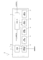
- FIG. 1 is a block diagram for explaining a transmitter including the position adjusting device of the first embodiment.
- the transmitter 1 illustrated in FIG. 1 includes a phase adjustment device 3 and an antenna 13.
- a transmitter including a phase adjustment device will be described as an example.
- the phase adjustment device of the first embodiment can also be applied to a receiver.
- the phase adjustment device 3 includes a phase shifter 11 that shifts the phase of the input signal W, a first control circuit 21 that sequentially changes the amount of phase shift of the phase shifter 11, and a phase-shifted shift input signal WS. And the phase difference signal that outputs the phase difference signal based on the phase difference between the shift input signal WS and the reference signal R.
- An output circuit 12 an extreme value output circuit 14 that acquires and outputs an extreme value of a phase difference signal obtained when the first control circuit 21 sequentially changes the phase shift amount of the phase shifter 11, and an extreme value output
- a target value output circuit that sets and outputs a target value based on the extreme value output from the circuit 14, and the extreme value and target value output from the phase difference signal output circuit 12 are input so that the extreme value becomes the target value.
- the phase-shifted shift input signal WS is supplied to the antenna 13 via the distributor 15 and output to the outside as a transmission wave.
- the input signal W is generated by a signal source (not shown), and the reference signal R is generated by a signal generator (not shown).
- the signal source and the signal generation unit are provided in a device in which the transmitter 1 is provided. As such a device, for example, a collision prevention system mounted on a vehicle can be considered.
- the phase shifter 11 shifts the phase of the input signal W and outputs a shift input signal WS.
- the first control circuit 21 sequentially changes the phase shift amount of the phase shifter 11. As a specific process for changing the shift amount, for example, the first control circuit 21 may sweep the phase shift amount of the phase shifter 11 within a range of 180 degrees or more. Further, for example, the first control circuit 21 can repeatedly change the phase shift amount of the phase shifter 11 at regular intervals within a range from 60 degrees to 240 degrees.
- the distributor 15 receives the shift input signal WS.
- the distributor 15 distributes the input shift input signal WS to the antenna 13 and the phase difference signal output circuit 12.
- the phase difference signal output circuit 12 receives the shift input signal WS and the reference signal R.
- the phase difference signal output circuit 12 outputs a phase difference signal based on the phase difference between the shift input signal WS and the reference signal R.
- the phase difference signal output circuit according to the first embodiment includes a down-conversion mixer, which will be described later, and a low-pass filter provided in the subsequent stage of the down-conversion mixer.
- the phase difference signal output circuit 12 generates and outputs a phase difference signal corresponding to the phase difference between the shift input signal WS and the reference signal R by performing frequency conversion with a down conversion mixer.
- the signal corresponding to the phase difference between the shift input signal WS output from the down-conversion mixer and the reference signal R is expressed by the following equations (1), (2), and (3).
- the shift input signal WS is expressed by the following equation (1) and the reference signal R is expressed by the following equation (2).
- f is a frequency
- t is time
- ⁇ is a phase difference.
- the frequency of the shift input signal WS and the frequency of the reference signal R are the same.
- the output V of the down-conversion mixer is expressed by the following equation (3).
- the output V expressed by Expression (3) is a DC signal corresponding to the phase difference ⁇ .
- K is a conversion gain of the down-conversion mixer
- D is the power of the input signal W
- E is the power of the reference signal R.
- the high-frequency component generated as a secondary is omitted because it is removed by the low-pass filter.
- generates the phase difference signal of 1st Embodiment is not limited to what performs the calculation as described in Formula (3) using the above-mentioned down conversion mixer and a low-pass filter.
- the configuration for removing the secondary high-frequency component is not limited to the low-pass filter, and may be, for example, an averaging processing circuit.
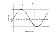
- FIG. 2 is a diagram showing the relationship between the phase shift amount changed by the first control circuit 21 and the phase difference signal output from the phase difference signal output circuit 12.
- the vertical axis of the graph shown in FIG. 2 indicates the phase difference signal output from the phase difference signal output circuit 12, and the horizontal axis indicates the phase shift amount changed by the first control circuit 21.
- the first control circuit 21 sweeps the phase shift amount of the phase shifter 11 in the range from 60 degrees to 240 degrees, the range from 60 degrees to 240 degrees indicated by the broken line square portion S shown in FIG.
- the phase difference signal corresponding to the phase shift amount is output from the phase difference signal output circuit 12.
- the curve P shown in FIG. 2 is represented by Expression (3). Each coefficient in equation (3) is unknown. According to the curve P shown in FIG. 2, a point G at which the curve has a maximum value or a minimum value at a certain phase is obtained.
- the absolute value g of the maximum value or the minimum value at the point G corresponds to ⁇ K ⁇ D ⁇ E / 2 in the equation (3).
- the maximum value and the minimum value are collectively referred to as “extreme value”.
- the extreme value output circuit 14 acquires the absolute value g of the maximum value or the minimum value from the value of the phase difference signal stored in a memory (not shown) and outputs the absolute value g.
- phase difference between the shift input signal WS and the reference signal R is adjusted to ⁇ 1. If the phase difference between the shift input signal WS and the reference signal R is ⁇ 1, the value of the phase difference signal output from the phase difference signal output circuit 12 is g ⁇ sin ⁇ 1. By utilizing this, in the first embodiment, when the phase difference between the shift input signal WS and the reference signal R is to be adjusted to ⁇ 1, the value of the phase difference signal output from the phase difference signal output circuit 12 is g ⁇ sin ⁇ 1. Thus, the phase shift amount of the phase shifter 11 is adjusted.
- the target value output circuit 16 generates a second target value g ⁇ sin ⁇ 1 of the phase difference signal from the absolute value g output from the extreme value output circuit 14 and the target phase difference ⁇ 1 between the shift input signal WS and the reference signal R. Is output to the control circuit 22.
- the target phase difference ⁇ 1 between the shift input signal WS and the reference signal R may be input from the outside, or may be a value held by the target value output circuit 16.
- phase difference signal output from the phase difference signal output circuit 12 and the target value output from the target value output circuit 16 are input to the second control circuit 22.
- the second control circuit 22 controls the phase shift amount of the phase shifter 11 so that the phase difference signal matches the target value.
- “so that the phase difference signal and the target value match” specifically means that the difference between the phase difference signal and the target value is equal to or less than a predetermined value.
- the phase difference signal and the target value input to the second control circuit 22 are both A / D converted digital signals.
- phase shifter 11 shifts the phase of the input signal W according to the phase shift amount controlled by the second control circuit 22. Due to the phase shift, the input signal W becomes a shift input signal WS whose phase is advanced by the target phase difference ⁇ 1 with respect to the reference signal R.
- the shift input signal WS is supplied to the antenna 13.
- the antenna 13 outputs a shift input signal WS whose phase is advanced by the target phase difference ⁇ 1 with respect to the reference signal R as a transmission wave.
- the conversion gain K of the down-conversion mixer, the power D of the input signal W, and the power E of the reference signal R vary depending on the ambient temperature, and the absolute value g of the extreme value of the phase difference signal also changes to the ambient temperature. Will change accordingly. Since the absolute value g according to the ambient temperature can be acquired in the first embodiment, the phase of the transmission wave can be controlled to an arbitrary value with high accuracy regardless of the ambient temperature.
- the transmitter of the first embodiment is not limited to the configuration described above. That is, in the above description, the case where the transmitter has one antenna and the phase difference between the transmission wave output from one antenna and the reference signal is adjusted to a desired phase difference has been described. However, the first embodiment may be applied to a transmitter having a plurality of antennas, in which the phase difference of transmission waves output from the plurality of antennas is set to a desired phase difference.
- the phase difference between the transmission wave W2 output from the antenna A and the transmission wave W3 output from the antenna B is expressed as ⁇ 2-.
- the phase difference between the transmission wave W2 output from the antenna A and the reference signal R is ⁇ 2
- the phase difference between the transmission wave W3 output from the antenna B and the reference signal R is ⁇ 3.
- the phase difference between the transmission wave of antenna A and the transmission wave of antenna B can be set to ⁇ 2 ⁇ 3.
- the first control circuit 21 and the second control circuit 22 are separate configurations, but the first embodiment is not limited to such a configuration.
- the transmitter according to the first embodiment may share some circuits between the first control circuit 21 and the second control circuit 22.
- FIG. 3 is a block diagram for explaining the transmitter 7 of the second embodiment.
- the transmitter 7 of the second embodiment includes a phase adjustment device 33 and an antenna 13.
- the phase adjustment device 33 is different from the transmitter 1 in that it has a processor 6 instead of the extreme value output circuit 14, the target value output circuit 16, the first control circuit 21, and the second control circuit 22 of the phase adjustment device 1. It is different.
- the extreme value output circuit 14, the target value output circuit 16, the first control circuit 21, and the second control circuit 22 of the first embodiment are hardware configured by circuit elements, and the processor 6 is a CPU. This is a combination of computer hardware including memory and memory and a program running on the computer.
- FIG. 4 is a flowchart for explaining the phase adjustment processing performed by the processor 6 shown in FIG.
- the processor 6 starts phase adjustment (calibration).
- the processor 6 receives the phase difference ⁇ between the desired phase of the transmission wave W and the reference signal R.
- the processor 6 sets a condition for adjusting the phase difference to an initial value. For example, the initial value of the control signal input to the transmitter 7 first, and the initial phase set in the phase shifter 11 when the processor 6 changes the phase of the phase shifter 11 by a certain value. This refers to the range of phase change.
- step S83 the processor 6 stores the value of the phase difference signal output from the phase difference signal output circuit 12 in a memory (not shown).
- step S84 the processor 6 determines whether or not the value of the phase difference signal has been recorded in the entire phase change range set in step S82. If it is determined in step S84 that the phase difference signal DC value has not yet been recorded in the entire phase change range (step S84: No), the phase control setting is incremented in step S89, that is, the phase is shifted by one step. change. Then, in step S83, the processor 6 stores the phase difference signal output in a state where the phase is changed in a memory (not shown).
- step S84 when recording of the phase difference signal DC is completed in the entire phase change range (step S84: Yes), the processor 6 calculates the value of the phase difference signal DC stored in a memory (not shown). Then, the absolute value g of the maximum value or the minimum value is specified (step S85).
- step S86 the processor 6 calculates the value V of g ⁇ sin ⁇ from the specified absolute value g and ⁇ input in step S81.
- step S87 the phase difference signal DC output from the phase difference signal output circuit 12 is read.
- step S88 whether or not the value of the phase difference signal DC matches V calculated in step S86 within an allowable range.
- step S90 the processor 6 increments the phase control setting by one step.
- step S87 the processor 6 next reads the phase difference signal DC output from the phase adjusting device 3. On the other hand, if the phase difference signal DC matches V as a result of the determination in step S88 (step S88: Yes), the processor 6 completes the adjustment of the phase of the transmission wave W of the transmitter 7.
- the transmitter 7 can be calibrated using the processor 6. For this reason, the transmitter 7 can be calibrated by operating the program shown in FIG. 4 on a general-purpose personal computer without using a dedicated control circuit.
- FIG. 5 is a block diagram illustrating an example in which the communication device according to the first embodiment is configured as the receiver 9. 5, components similar to those illustrated in FIG. 1 are denoted by the same reference numerals, and description thereof is partially omitted.
- the receiver 9 includes a receiving unit 34, a receiving unit 35, and a control circuit 5.
- the receiving units 34 and 35 include a phase difference signal output circuit 29 that detects a phase difference between the reference signal and the detected signal and generates a phase difference signal corresponding to the detected phase difference.
- the phase difference signal output circuit 29 includes a down-conversion mixer 195 and a low-pass filter (denoted as “LPF” in the drawing) 193.
- the receiving units 34 and 35 include a phase shifter 11 that changes the phase of the signal to be detected.
- the control circuit 5 determines the amount of phase change in the phase shifter 11 corresponding to the phase difference signal generated by the phase difference signal output circuit 29.
- the detected signal is the input signal W received by the antenna 13, and the signal input to the phase difference signal output circuit 29 is the reference signal R.
- the receiving units 34 and 35 include a distributor 15 between the phase shifter 11 and the antenna 13. Between the phase difference signal output circuit 29 and the control circuit 5, an analog / digital converter (referred to as “ADC”) 21 is provided. The signal output from the phase difference signal output circuit 29 is A / D converted into a DC signal.
- the phase shifter 11 is provided in the local transmission path of the receiving units 34 and 35.
- the input signal W distributed to each channel is sent to the phase shifter 11 and the distributor 15.
- the input signal W distributed by the distributor 15 is input to the down conversion mixer 195 of the phase difference signal output circuit 29 together with the reference signal R.
- the down conversion mixer 195 outputs a signal corresponding to the phase difference between the input signal W and the reference signal R to the low pass filter 193.
- the low-pass filter 193 outputs a phase difference signal corresponding to the phase difference between the input signal W and the reference signal R to the ADC 25, and the ADC 25 converts the phase difference signal into a digital signal and outputs it to the control circuit 5 as the phase difference signal DC. Output.
- the control circuit 5 processes information according to a known procedure determined in advance, and outputs a necessary control signal C to the phase shifter 11 of the receiving units 34 and 35.
- the phase adjustment device of the first embodiment can be configured as either the transmitter 1 shown in FIG. 1 or the receiver 9 shown in FIG. By applying the position adjusting device of the first embodiment to the receiver 9, the phases of the local signals received by the plurality of receivers 9 can be made uniform.
- the present invention described above is suitable for the field of communication in which a high-frequency signal of about several tens of GHz is used as a transmission wave or a reception wave, and its phase needs to be controlled with high accuracy.
Landscapes
- Engineering & Computer Science (AREA)
- Radar, Positioning & Navigation (AREA)
- Remote Sensing (AREA)
- Computer Networks & Wireless Communication (AREA)
- Physics & Mathematics (AREA)
- General Physics & Mathematics (AREA)
- Signal Processing (AREA)
- Transmitters (AREA)
Abstract
Description
なお、本明細書では、ビームフォーミングを主にキャリア波を送信する側から説明する。しかし、ビームフォーミングでは、送信波を受信する側においても、任意の方向から送信された送信波を強く受信し、他の方向から送信された送信波を受信しないようにすることもできる。
図6は、位相シフタ11を備える公知の送信器を例示した機能ブロック図である。図6に示した送信器100a、100bは、信号源109によって生成された送信波を各々位相シフタ101でシフトさせ、パワーアンプ107を介してアンテナ103に供給する。アンテナ103は、パワーアンプ107で増幅された送信波を送信する。なお、位相シフタ101における位相のシフト量は、図示しない制御回路から出力される位相制御信号によって決定する。
このような送信器100a、100bを使って送信波の射出方向を動的に切替える場合、各アンテナに供給される送信波の位相を高い精度で選択することが求められる。なお、送信波の位相を動的に切替える位相シフタ11は、例えば、非特許文献1に記載されている。
このような高精度での位相の調整は、特に送信波が高周波数の分野において、既存の位相シフタ11を備える送信器では困難であった。
本発明は、このような点に鑑みてなされたものであり、数十GHz程度の高周波信号が送信波として使用される送信器において、送信波の位相を高い精度で任意の値に制御可能な送信器、送信方法、位相調整装置、位相調整方法を提供することを目的としている。
また、本発明の一態様の送信器は、上記態様において、前記第2の制御回路が、前記位相差信号出力回路から前記位相差信号を入力し、前記目標値出力回路から前記目標値を入力し、前記位相差信号が前記目標値と一致するように前記位相シフタの前記位相シフト量を制御する。
また、本発明の一態様の位相調整装置は、上記態様において、前記第2の制御回路が、前記位相差信号出力回路から前記位相差信号を入力し、前記目標値出力回路から前記目標値を入力し、前記位相差信号が前記目標値と一致するように前記位相シフタの前記位相シフト量を制御する。
[第1実施形態]
<送信器>
図1は、第1実施形態の位置調整装置を備えた送信器を説明するためのブロック図である。図1に示した送信器1は、位相調整装置3とアンテナ13とを備えている。
第1実施形態では、位相調整装置を備える送信器を例に説明するが、第1実施形態の位相調整装置は受信器に適用することも可能である。
位相調整装置3は、入力された入力信号Wの位相をシフトする位相シフタ11と、位相シフタ11の位相のシフト量を順次変更する第1の制御回路21と、位相シフトされたシフト入力信号WSを分配する分配器15と、分配器15により分配されたシフト入力信号WSと基準信号Rが入力され、シフト入力信号WSと基準信号Rとの位相差に基づく位相差信号を出力する位相差信号出力回路12と、第1の制御回路21が位相シフタ11の位相のシフト量を順次変更したときに得られる位相差信号の極値を取得して出力する極値出力回路14と、極値出力回路14が出力した極値に基づいて目標値を設定して出力する目標値出力回路と、位相差信号出力回路12が出力した極値と目標値が入力され、極値が目標値となるように位相シフタ11の位相のシフト量を制御する第2の制御回路22と、を備えている。
なお、第1実施形態においては、入力信号Wが図示しない信号源によって生成され、基準信号Rが図示しない信号生成部によって生成される。信号源及び信号生成部は、送信器1が設けられる機器に設けられているものとする。このような機器としては、例えば、車両に搭載された衝突予防システム等が考えられる。
(位相シフタ)
位相シフタ11は、入力信号Wの位相をシフトし、シフト入力信号WSを出力する。
(第1の制御回路)
第1の制御回路21は、位相シフタ11の位相のシフト量を順次変更する。シフト量を変更する具体的な処理としては、例えば、第1の制御回路21が位相シフタ11の位相のシフト量を180度以上の範囲でスイープすることが考えられる。また、例えば、第1の制御回路21は、位相シフタ11の位相のシフト量を60度から240度までの範囲において一定の間隔で繰返し変更することができる。
(分配器)
分配器15には、シフト入力信号WSが入力される。分配器15は、入力されたシフト入力信号WSをアンテナ13と位相差信号出力回路12とに分配する。
位相差信号出力回路12には、シフト入力信号WSと基準信号Rとが入力される。位相差信号出力回路12は、シフト入力信号WSと基準信号Rとの位相差に基づく位相差信号を出力する。第1実施形態の位相差信号出力回路は、後に図示するダウンコンバージョンミキサ及びダウンコンバージョンミキサの後段に設けられたローパスフィルタを有する。位相差信号出力回路12は、ダウンコンバージョンミキサで周波数変換を行うことによってシフト入力信号WSと基準信号Rとの位相差に対応する位相差信号を生成し、出力する。
シフト入力信号WSを式(1)、基準信号Rを式(2)として以下のように示す。式(1)、式(2)において、fは周波数、tは時間、θは位相差である。シフト入力信号WSの周波数と基準信号Rの周波数は同一である。



極値出力回路14には、第1の制御回路21が位相シフタ11の位相のシフト量を順次変更したときの、位相差信号出力回路12の出力が入力される。即ち、極値出力回路14には、式(3)中の位相差θが順次変更されたときの位相差信号が入力される。位相差信号は、極値出力回路14内の図示しないメモリに格納される。
第1の制御回路21が位相シフタ11の位相のシフト量を60度から240度までの範囲でスイープさせた場合、図2中に示した破線四角部Sが示す60度から240度までの範囲の位相シフト量に対応する位相差信号が位相差信号出力回路12から出力される。
極値出力回路14は、図示しないメモリ内に格納された位相差信号の値から極大値または極小値の絶対値gを取得して出力する。
目標値出力回路16の説明に先立って、先ず、シフト入力信号WSの位相を、基準信号Rとの位相差がθとなるように位相調整する方法を説明する。この位相調整は、送信器1の出荷前に製造者によって行われてもよい。また、位相調整は、出荷後にユーザによって用途や使用の目的に応じて任意に行われるものであってもよい。
シフト入力信号WSと基準信号Rとの位相差がθであった場合、位相差信号出力回路12が出力する位相差信号は式(3)によって表される。式(3)によって得られる-K×D×E/2の絶対値は、点Gにおける極大値または極小値の絶対値gとなる。絶対値gは、極値出力回路14が図5に示した曲線Pから算出することが可能となる。
目標値出力回路16は、極値出力回路14が出力する絶対値g及びシフト入力信号WSと基準信号Rとの目標位相差θ1から、位相差信号の目標値g×sinθ1を生成して第2の制御回路22に出力する。シフト入力信号WSと基準信号Rとの目標位相差θ1は、外部から入力されてもよいし、目標値出力回路16が保持している値であってもよい。
第2の制御回路22には、位相差信号出力回路12が出力する位相差信号と目標値出力回路16が出力した目標値とが入力される。第2の制御回路22は、位相差信号と目標値とが一致するように位相シフタ11の位相のシフト量を制御する。なお、本実施形態において、「位相差信号と目標値とが一致するとが一致するように」とは、具体的には位相差信号と目標値との差を所定値以下にすることをいう。また、第1実施形態では、第2の制御回路22に入力される位相差信号及び目標値が、いずれもA/D変換されたデジタル信号であるものとする。
位相シフタ11は、第2の制御回路22によって制御される位相のシフト量にしたがって入力信号Wの位相をシフトする。位相のシフトにより、入力信号Wは、基準信号Rに対して目標位相差θ1だけ位相が進んだシフト入力信号WSとなる。シフト入力信号WSは、アンテナ13に供給される。
(アンテナ)
アンテナ13は、基準信号Rに対して目標位相差θ1だけ位相が進んだシフト入力信号WSを送信波として出力する。
公知の送信器において、ダウンコンバージョンミキサの変換ゲインKや入力信号WのパワーD、基準信号RのパワーEは周囲温度に応じて変動し、位相差信号の極値の絶対値gも周囲温度に応じて変化する。第1実施形態は、周囲温度に応じた絶対値gを取得することが可能であるため、周囲温度によらず、送信波の位相を高い精度で任意の値に制御することが可能である。
なお、第1実施形態の送信器は、以上説明した構成に限定されるものではない。即ち、以上の説明では、送信器が1つのアンテナを備え、1つのアンテナから出力される送信波と基準信号との位相差を所望の位相差に調整する場合を説明した。しかし、第1実施形態は、アンテナを複数備えた送信器において、複数のアンテナから出力される送信波の位相差を所望の位相差にする場合に適用してもよい。
また、上記した構成では、第1の制御回路21と第2の制御回路22とを別個の構成としたが、第1実施形態は、このような構成に限定されるものではない。第1実施形態の送信器は、第1の制御回路21と第2の制御回路22との間で一部の回路を共用してもよい。
図3は、第2実施形態の送信器7を説明するためのブロック図である。図3において、図1に示した構成と同様の構成については同様の符号を付して示している。第2実施形態の送信器7は、位相調整装置33とアンテナ13を有している。位相調整装置33は、位相調整装置1の極値出力回路14、目標値出力回路16、第1の制御回路21及び第2の制御回路22に代えて、プロセッサ6を有する点で送信器1と相違している。なお、第1実施形態の極値出力回路14、目標値出力回路16、第1の制御回路21及び第2の制御回路22は、回路素子で構成されるハードウェアであり、プロセッサ6は、CPUやメモリを含むコンピュータのハードウェアと、コンピュータ上で動作するプログラムを合わせたものである。
ステップS81において、プロセッサ6は、位相の調整(キャリブレーション)を開始する。このとき、プロセッサ6には、送信波Wの所望の位相と基準信号Rとの位相差θが入力される。次に、ステップS82において、プロセッサ6は、位相差の調整を行う際の条件を初期値に設定する。この設定は、例えば、最初に送信器7に入力される制御信号の初期値や、プロセッサ6が位相シフタ11の位相を一定の値ずつ変更するにあたり、位相シフタ11に設定される最初の位相及び位相の変更範囲等をいう。
また、ステップS84において、位相の全変範囲において位相差信号DCの記録が完了している場合(ステップS84:Yes)、プロセッサ6は、図示しないメモリに保存されている位相差信号DCの値から、極大値または極小値の絶対値gを特定する(ステップS85)。
一方、ステップS88の判断の結果、位相差信号DCがVと一致している場合(ステップS88:Yes)、プロセッサ6は、送信器7の送信波Wの位相の調整を完了する。
以上説明した第1実施形態及び第2実施形態は、いずれも位相調整装置を送信器に適用した例を示した。しかし、第1実施形態及び第2実施形態の位相調整装置は、送信器として構成されるものに限定されるものでなく、受信器として構成することも可能である。
図5は、第1実施形態の通信装置を受信器9として構成した例を示したブロック図である。図5において、図1に示した構成と同様の構成については同様の符号を付し、説明を一部略す。
また、受信部34、35は、被検出信号の位相を変化させる位相シフタ11を備えている。制御回路5は、位相差信号出力回路29によって生成された位相差信号に対応して位相シフタ11における位相の変化量を決定する。受信器9において、図1に示した極値出力回路14、目標値出力回路16、第1の制御回路21及び第2の制御回路22の機能は、制御回路5が行うものとする。
また、受信部34、35は、位相シフタ11とアンテナ13との間に分配器15を備えている。位相差信号出力回路29と制御回路5との間にはアナログ・デジタル変換器(図中に「ADC」と記す)21をそれぞれ備えている。位相差信号出力回路29から出力される信号は、A/D変換されてDC信号となっている。
位相シフタ11は、受信部34、35のローカル伝送経路に設けられる。各チャネルに分配された入力信号Wは、位相シフタ11及び分配器15に送られる。分配器15によって分配された入力信号Wは、基準信号Rと共に位相差信号出力回路29のダウンコンバージョンミキサ195に入力される。
制御回路5は、予め決められた公知の手順に従って情報を処理し、必要な制御信号Cを受信部34、35の位相シフタ11へ出力する。
以上説明したように、第1実施形態の位相調整装置は、図1に示した送信器1、図5に示した受信器9のいずれとしても構成することができる。第1実施形態の位置調整装置を受信器9に適用することにより、複数の受信器9が受信するローカル信号の位相を揃えることもできる。
3、33 位相調整装置
5 制御回路
6 プロセッサ
9 受信器
11 位相シフタ
12 位相差信号出力回路
13 アンテナ
14 極値出力回路
15 分配器
16 目標値出力回路
21 第1の制御回路
22 第2の制御回路
25 ADC
29 位相差信号出力回路
33 受信部
34、35 受信部
193 ローパスフィルタ
195 ダウンコンバージョンミキサ
Claims (6)
- 入力信号の位相をシフトし、位相がシフトされたシフト信号を出力する位相シフタと、
前記位相シフタが前記入力信号の位相をシフトする位相シフト量を予め定められた範囲で変更する第1の制御回路と、
前記位相シフタによって出力された前記シフト信号と基準信号とが入力され、前記シフト信号と前記基準信号との位相差に基づく位相差信号を出力する位相差信号出力回路と、
前記第1の制御回路が前記位相シフト量を変更している間に前記位相差信号が極値をとる場合、前記位相差信号が前記極値となる前記位相シフト量での前記位相差信号の値を出力する極値出力回路と、
前記極値出力回路の出力に基づいて目標値を出力する目標値出力回路と、
前記位相差信号出力回路によって出力される前記位相差信号の値が、前記目標値出力回路から出力される前記目標値と一致するように、前記位相シフタの前記位相シフト量を制御する第2の制御回路と、を備え、
前記位相シフタは、前記第2の制御回路によって制御された前記位相シフト量で前記入力信号の位相をシフトし、位相がシフトされた前記入力信号を送信波として出力する送信器。 - 前記第2の制御回路は、前記位相差信号出力回路から前記位相差信号を入力し、前記目標値出力回路から前記目標値を入力し、前記位相差信号が前記目標値と一致するように前記位相シフタの前記位相シフト量を制御する請求項1に記載の送信器。
- 入力信号の位相を、予め設定された位相の範囲でシフトする第1の位相シフトステップと、
前記第1の位相シフトステップにおいて位相がシフトされた前記入力信号と基準信号との位相差に基づく位相差信号を生成する位相差信号生成ステップと、
前記第1の位相シフトステップにおいて前記入力信号の位相がシフトされている間に前記位相差信号が極値をとる場合、前記位相差信号が前記極値となる位相シフト量での前記位相差信号の値を出力する極値出力ステップと、
前記極値出力ステップにおいて出力された前記位相差信号の値に基づいて目標値を出力する目標値出力ステップと、
前記位相差信号生成ステップにおいて生成された前記位相差信号の値が前記目標値と一致するように前記入力信号の位相をシフトする第2の位相シフトステップと、を含み、
前記第2の位相シフトステップで位相をシフトされた前記入力信号を送信波として出力する送信方法。 - 入力信号の位相をシフトし、位相がシフトされたシフト信号を出力する位相シフタと、
前記位相シフタが前記入力信号の位相をシフトする位相シフト量を予め定められた範囲で変更する第1の制御回路と、
前記位相シフタによって出力された前記シフト信号と基準信号とが入力され、前記シフト信号と前記基準信号との位相差に基づく位相差信号を出力する位相差信号出力回路と、
前記第1の制御回路が前記位相シフト量を変更している間に前記位相差信号が極値をとる場合、前記位相差信号の前記極値を出力する極値出力回路と、
前記極値出力回路によって出力された前記極値に基づいて設定される目標値を出力する目標値出力回路と、
前記位相差信号出力回路によって出力される前記位相差信号の値が、前記目標値出力回路から出力される前記目標値と一致するように、前記位相シフタの前記位相シフト量を制御する第2の制御回路と、を備える位相調整装置。 - 前記第2の制御回路は、前記位相差信号出力回路から前記位相差信号を入力し、前記目標値出力回路から前記目標値を入力し、前記位相差信号が前記目標値と一致するように前記位相シフタの前記位相シフト量を制御する請求項4に記載の位相調整装置。
- 入力信号の位相を、予め設定された位相の範囲でシフトする第1の位相シフトステップと、
前記第1の位相シフトステップにおいて位相がシフトされた前記入力信号と基準信号との位相差に基づく位相差信号を生成する位相差信号生成ステップと、
前記第1の位相シフトステップにおいて前記入力信号の位相がシフトされている間に前記位相差信号が極値をとる場合、前記位相差信号が前記極値となる位相シフト量での前記位相差信号の値を出力する極値出力ステップと、
前記極値出力ステップにおいて出力された前記位相差信号の値に基づいて目標値を出力する目標値出力ステップと、
前記位相差信号生成ステップにおいて生成された前記位相差信号の値が前記目標値と一致するように前記入力信号の位相をシフトする第2の位相シフトステップと、を含む位相調整方法。
Priority Applications (3)
| Application Number | Priority Date | Filing Date | Title |
|---|---|---|---|
| DE112016000190.8T DE112016000190B4 (de) | 2015-04-13 | 2016-04-12 | Sender, Sendeverfahren, Phasenjustiervorrichtung und Phasenjustierverfahren |
| US15/541,803 US10330775B2 (en) | 2015-04-13 | 2016-04-12 | Transmitter, transmission method, phase adjustment device, and phase adjustment method |
| JP2017512542A JP6295011B2 (ja) | 2015-04-13 | 2016-04-12 | 送信器、送信方法、位相調整装置、位相調整方法 |
Applications Claiming Priority (2)
| Application Number | Priority Date | Filing Date | Title |
|---|---|---|---|
| JP2015-081697 | 2015-04-13 | ||
| JP2015081697 | 2015-04-13 |
Publications (1)
| Publication Number | Publication Date |
|---|---|
| WO2016167253A1 true WO2016167253A1 (ja) | 2016-10-20 |
Family
ID=57126764
Family Applications (1)
| Application Number | Title | Priority Date | Filing Date |
|---|---|---|---|
| PCT/JP2016/061815 Ceased WO2016167253A1 (ja) | 2015-04-13 | 2016-04-12 | 送信器、送信方法、位相調整装置、位相調整方法 |
Country Status (4)
| Country | Link |
|---|---|
| US (1) | US10330775B2 (ja) |
| JP (1) | JP6295011B2 (ja) |
| DE (1) | DE112016000190B4 (ja) |
| WO (1) | WO2016167253A1 (ja) |
Cited By (5)
| Publication number | Priority date | Publication date | Assignee | Title |
|---|---|---|---|---|
| WO2020044959A1 (ja) | 2018-08-29 | 2020-03-05 | 京セラ株式会社 | 電子機器、電子機器の制御方法、及び電子機器の制御プログラム |
| WO2020066498A1 (ja) | 2018-09-26 | 2020-04-02 | 京セラ株式会社 | 電子機器、電子機器の制御方法、及び電子機器の制御プログラム |
| WO2020075689A1 (ja) | 2018-10-12 | 2020-04-16 | 京セラ株式会社 | 電子機器、電子機器の制御方法、及び電子機器の制御プログラム |
| JP2020202453A (ja) * | 2019-06-07 | 2020-12-17 | 旭化成エレクトロニクス株式会社 | 位相調整回路及び位相調整方法 |
| KR20210063386A (ko) * | 2018-09-27 | 2021-06-01 | 로베르트 보쉬 게엠베하 | 동기화된 고주파 모듈들을 구비한 레이더 센서 |
Families Citing this family (3)
| Publication number | Priority date | Publication date | Assignee | Title |
|---|---|---|---|---|
| KR102630934B1 (ko) | 2016-05-13 | 2024-01-30 | 삼성전자주식회사 | 무선 전력 송신기 및 그 제어 방법 |
| US10374465B2 (en) * | 2016-05-13 | 2019-08-06 | Samsung Electronics Co., Ltd. | Wireless power transmitter and control method therefor |
| US11448745B2 (en) | 2018-06-22 | 2022-09-20 | Asahi Kasei Microdevices Corporation | Sensor device and system, and biometric sensing method and system |
Citations (4)
| Publication number | Priority date | Publication date | Assignee | Title |
|---|---|---|---|---|
| JPH11225014A (ja) * | 1998-02-05 | 1999-08-17 | Nec Corp | フェーズドアレイレーダ装置及びその位相校正方法 |
| JP2003307561A (ja) * | 2002-04-12 | 2003-10-31 | Fuji Heavy Ind Ltd | 車両用運転支援装置 |
| WO2004109952A1 (ja) * | 2003-06-02 | 2004-12-16 | Fujitsu Limited | アレーアンテナ通信装置およびアレーアンテナ通信装置のキャリブレーション方法 |
| JP2006304205A (ja) * | 2005-04-25 | 2006-11-02 | Nippon Hoso Kyokai <Nhk> | アンテナ位相較正装置及びそれを用いた追尾アンテナ装置 |
Family Cites Families (10)
| Publication number | Priority date | Publication date | Assignee | Title |
|---|---|---|---|---|
| US4829257A (en) * | 1987-02-20 | 1989-05-09 | Cooper J Carl | Method and apparatus for continuously shifting phase of an electronic signal |
| US6400318B1 (en) * | 1999-04-30 | 2002-06-04 | Kabushiki Kaisha Toshiba | Adaptive array antenna |
| JP3564077B2 (ja) * | 2001-03-29 | 2004-09-08 | 独立行政法人情報通信研究機構 | 光制御フェーズドアレイアンテナの位相制御装置および光制御フェーズドアレイアンテナ・システム |
| US7999624B2 (en) * | 2007-04-24 | 2011-08-16 | City University Of Hong Kong | Radiation source |
| JP4562787B2 (ja) * | 2008-07-30 | 2010-10-13 | ルネサスエレクトロニクス株式会社 | Pll回路 |
| US8456250B2 (en) * | 2009-02-04 | 2013-06-04 | Sand 9, Inc. | Methods and apparatus for tuning devices having resonators |
| JP5672092B2 (ja) * | 2011-03-17 | 2015-02-18 | 株式会社リコー | スペクトラム拡散クロック発生回路 |
| CN103477570B (zh) * | 2011-08-02 | 2016-04-27 | 松下电器产业株式会社 | 相控阵发送装置 |
| TWI518993B (zh) * | 2012-11-20 | 2016-01-21 | 財團法人工業技術研究院 | 具可調式相移陣列的多路徑切換系統 |
| JP5933471B2 (ja) * | 2013-03-14 | 2016-06-08 | パナソニック株式会社 | フェーズドアレイ送信装置 |
-
2016
- 2016-04-12 DE DE112016000190.8T patent/DE112016000190B4/de active Active
- 2016-04-12 WO PCT/JP2016/061815 patent/WO2016167253A1/ja not_active Ceased
- 2016-04-12 JP JP2017512542A patent/JP6295011B2/ja active Active
- 2016-04-12 US US15/541,803 patent/US10330775B2/en active Active
Patent Citations (4)
| Publication number | Priority date | Publication date | Assignee | Title |
|---|---|---|---|---|
| JPH11225014A (ja) * | 1998-02-05 | 1999-08-17 | Nec Corp | フェーズドアレイレーダ装置及びその位相校正方法 |
| JP2003307561A (ja) * | 2002-04-12 | 2003-10-31 | Fuji Heavy Ind Ltd | 車両用運転支援装置 |
| WO2004109952A1 (ja) * | 2003-06-02 | 2004-12-16 | Fujitsu Limited | アレーアンテナ通信装置およびアレーアンテナ通信装置のキャリブレーション方法 |
| JP2006304205A (ja) * | 2005-04-25 | 2006-11-02 | Nippon Hoso Kyokai <Nhk> | アンテナ位相較正装置及びそれを用いた追尾アンテナ装置 |
Cited By (9)
| Publication number | Priority date | Publication date | Assignee | Title |
|---|---|---|---|---|
| WO2020044959A1 (ja) | 2018-08-29 | 2020-03-05 | 京セラ株式会社 | 電子機器、電子機器の制御方法、及び電子機器の制御プログラム |
| US12007497B2 (en) | 2018-08-29 | 2024-06-11 | Kyocera Corporation | Electronic device, control method of electronic device, and control program of electronic device |
| WO2020066498A1 (ja) | 2018-09-26 | 2020-04-02 | 京セラ株式会社 | 電子機器、電子機器の制御方法、及び電子機器の制御プログラム |
| KR20210063386A (ko) * | 2018-09-27 | 2021-06-01 | 로베르트 보쉬 게엠베하 | 동기화된 고주파 모듈들을 구비한 레이더 센서 |
| KR102829336B1 (ko) * | 2018-09-27 | 2025-07-03 | 로베르트 보쉬 게엠베하 | 동기화된 고주파 모듈들을 구비한 레이더 센서 |
| WO2020075689A1 (ja) | 2018-10-12 | 2020-04-16 | 京セラ株式会社 | 電子機器、電子機器の制御方法、及び電子機器の制御プログラム |
| JP2020202453A (ja) * | 2019-06-07 | 2020-12-17 | 旭化成エレクトロニクス株式会社 | 位相調整回路及び位相調整方法 |
| US11411312B2 (en) * | 2019-06-07 | 2022-08-09 | Asahi Kasei Microdevices Corporation | Phase adjusting circuit and phase adjusting method |
| JP7161822B2 (ja) | 2019-06-07 | 2022-10-27 | 旭化成エレクトロニクス株式会社 | 位相調整回路及び位相調整方法 |
Also Published As
| Publication number | Publication date |
|---|---|
| DE112016000190T5 (de) | 2017-08-24 |
| DE112016000190B4 (de) | 2019-03-28 |
| JP6295011B2 (ja) | 2018-03-14 |
| JPWO2016167253A1 (ja) | 2017-10-12 |
| US20180003801A1 (en) | 2018-01-04 |
| US10330775B2 (en) | 2019-06-25 |
Similar Documents
| Publication | Publication Date | Title |
|---|---|---|
| JP6295011B2 (ja) | 送信器、送信方法、位相調整装置、位相調整方法 | |
| EP2975781B1 (en) | Phased array transmission device | |
| US9031163B2 (en) | Phased array transmission device | |
| US9525205B2 (en) | Beam forming device and method for forming beam using the same | |
| JP6479155B2 (ja) | Fm−cwレーダおよびfm−cw信号の生成方法 | |
| JP6701124B2 (ja) | レーダ装置 | |
| US20170257137A1 (en) | Active phased array transmitter, active phased array receiver, and active phased array transceiver | |
| US10177830B2 (en) | Array antenna system | |
| US9432075B2 (en) | Communication apparatus and phase adjustment method | |
| WO2017199296A1 (ja) | Fm-cwレーダおよびfm-cw信号の生成方法 | |
| US10505770B2 (en) | Reception signal processing device, radar, and object detection method | |
| EP3252496A1 (en) | Radar device and transmission power control method | |
| KR102313253B1 (ko) | 무선 주파수 장치 및 대응 방법 | |
| WO2014045928A1 (ja) | パルス圧縮レーダ | |
| KR101547986B1 (ko) | 자체 송신 신호를 이용한 모노펄스 추적 시스템의 자동 위상 정합 및 안테나 추적 각도 정합 장치와 그 방법 | |
| JP6532017B2 (ja) | フェーズドアレイ送信装置 | |
| WO2016084468A1 (ja) | レーダ装置、レーダ出力調整システム、及びレーダ出力調整方法 | |
| US10212011B2 (en) | Wireless device and method for controlling phase | |
| JP2017005647A (ja) | 位相制御装置及びアレーアンテナシステム | |
| JP5306516B2 (ja) | 測位装置 | |
| KR101808905B1 (ko) | 송신 경로 교정 장치 및 방법 | |
| JP2019158690A (ja) | レーダ装置およびレーダ装置の調整方法 | |
| WO2025006555A2 (en) | Self-calibration method of the phase shifter for phased-array radar applications | |
| JP2016092635A (ja) | アクティブアンテナシステム | |
| JP2017005656A (ja) | 位相異常検出装置及びアレーアンテナシステム |
Legal Events
| Date | Code | Title | Description |
|---|---|---|---|
| 121 | Ep: the epo has been informed by wipo that ep was designated in this application |
Ref document number: 16780044 Country of ref document: EP Kind code of ref document: A1 |
|
| ENP | Entry into the national phase |
Ref document number: 2017512542 Country of ref document: JP Kind code of ref document: A |
|
| WWE | Wipo information: entry into national phase |
Ref document number: 112016000190 Country of ref document: DE |
|
| WWE | Wipo information: entry into national phase |
Ref document number: 15541803 Country of ref document: US |
|
| 122 | Ep: pct application non-entry in european phase |
Ref document number: 16780044 Country of ref document: EP Kind code of ref document: A1 |