WO2016167093A1 - 光デバイスパッケージ - Google Patents
光デバイスパッケージ Download PDFInfo
- Publication number
- WO2016167093A1 WO2016167093A1 PCT/JP2016/059242 JP2016059242W WO2016167093A1 WO 2016167093 A1 WO2016167093 A1 WO 2016167093A1 JP 2016059242 W JP2016059242 W JP 2016059242W WO 2016167093 A1 WO2016167093 A1 WO 2016167093A1
- Authority
- WO
- WIPO (PCT)
- Prior art keywords
- optical device
- lcos
- package
- light
- device package
- Prior art date
- Legal status (The legal status is an assumption and is not a legal conclusion. Google has not performed a legal analysis and makes no representation as to the accuracy of the status listed.)
- Ceased
Links
Images





Classifications
-
- G—PHYSICS
- G02—OPTICS
- G02F—OPTICAL DEVICES OR ARRANGEMENTS FOR THE CONTROL OF LIGHT BY MODIFICATION OF THE OPTICAL PROPERTIES OF THE MEDIA OF THE ELEMENTS INVOLVED THEREIN; NON-LINEAR OPTICS; FREQUENCY-CHANGING OF LIGHT; OPTICAL LOGIC ELEMENTS; OPTICAL ANALOGUE/DIGITAL CONVERTERS
- G02F1/00—Devices or arrangements for the control of the intensity, colour, phase, polarisation or direction of light arriving from an independent light source, e.g. switching, gating or modulating; Non-linear optics
- G02F1/01—Devices or arrangements for the control of the intensity, colour, phase, polarisation or direction of light arriving from an independent light source, e.g. switching, gating or modulating; Non-linear optics for the control of the intensity, phase, polarisation or colour
- G02F1/13—Devices or arrangements for the control of the intensity, colour, phase, polarisation or direction of light arriving from an independent light source, e.g. switching, gating or modulating; Non-linear optics for the control of the intensity, phase, polarisation or colour based on liquid crystals, e.g. single liquid crystal display cells
- G02F1/133—Constructional arrangements; Operation of liquid crystal cells; Circuit arrangements
- G02F1/1333—Constructional arrangements; Manufacturing methods
- G02F1/133308—Support structures for LCD panels, e.g. frames or bezels
-
- G—PHYSICS
- G02—OPTICS
- G02F—OPTICAL DEVICES OR ARRANGEMENTS FOR THE CONTROL OF LIGHT BY MODIFICATION OF THE OPTICAL PROPERTIES OF THE MEDIA OF THE ELEMENTS INVOLVED THEREIN; NON-LINEAR OPTICS; FREQUENCY-CHANGING OF LIGHT; OPTICAL LOGIC ELEMENTS; OPTICAL ANALOGUE/DIGITAL CONVERTERS
- G02F1/00—Devices or arrangements for the control of the intensity, colour, phase, polarisation or direction of light arriving from an independent light source, e.g. switching, gating or modulating; Non-linear optics
- G02F1/01—Devices or arrangements for the control of the intensity, colour, phase, polarisation or direction of light arriving from an independent light source, e.g. switching, gating or modulating; Non-linear optics for the control of the intensity, phase, polarisation or colour
- G02F1/13—Devices or arrangements for the control of the intensity, colour, phase, polarisation or direction of light arriving from an independent light source, e.g. switching, gating or modulating; Non-linear optics for the control of the intensity, phase, polarisation or colour based on liquid crystals, e.g. single liquid crystal display cells
- G02F1/133—Constructional arrangements; Operation of liquid crystal cells; Circuit arrangements
- G02F1/1333—Constructional arrangements; Manufacturing methods
- G02F1/133382—Heating or cooling of liquid crystal cells other than for activation, e.g. circuits or arrangements for temperature control, stabilisation or uniform distribution over the cell
-
- G—PHYSICS
- G02—OPTICS
- G02F—OPTICAL DEVICES OR ARRANGEMENTS FOR THE CONTROL OF LIGHT BY MODIFICATION OF THE OPTICAL PROPERTIES OF THE MEDIA OF THE ELEMENTS INVOLVED THEREIN; NON-LINEAR OPTICS; FREQUENCY-CHANGING OF LIGHT; OPTICAL LOGIC ELEMENTS; OPTICAL ANALOGUE/DIGITAL CONVERTERS
- G02F1/00—Devices or arrangements for the control of the intensity, colour, phase, polarisation or direction of light arriving from an independent light source, e.g. switching, gating or modulating; Non-linear optics
- G02F1/01—Devices or arrangements for the control of the intensity, colour, phase, polarisation or direction of light arriving from an independent light source, e.g. switching, gating or modulating; Non-linear optics for the control of the intensity, phase, polarisation or colour
- G02F1/13—Devices or arrangements for the control of the intensity, colour, phase, polarisation or direction of light arriving from an independent light source, e.g. switching, gating or modulating; Non-linear optics for the control of the intensity, phase, polarisation or colour based on liquid crystals, e.g. single liquid crystal display cells
- G02F1/133—Constructional arrangements; Operation of liquid crystal cells; Circuit arrangements
- G02F1/136—Liquid crystal cells structurally associated with a semi-conducting layer or substrate, e.g. cells forming part of an integrated circuit
- G02F1/1362—Active matrix addressed cells
- G02F1/136277—Active matrix addressed cells formed on a semiconductor substrate, e.g. of silicon
-
- H—ELECTRICITY
- H10—SEMICONDUCTOR DEVICES; ELECTRIC SOLID-STATE DEVICES NOT OTHERWISE PROVIDED FOR
- H10F—INORGANIC SEMICONDUCTOR DEVICES SENSITIVE TO INFRARED RADIATION, LIGHT, ELECTROMAGNETIC RADIATION OF SHORTER WAVELENGTH OR CORPUSCULAR RADIATION
- H10F39/00—Integrated devices, or assemblies of multiple devices, comprising at least one element covered by group H10F30/00, e.g. radiation detectors comprising photodiode arrays
- H10F39/80—Constructional details of image sensors
- H10F39/804—Containers or encapsulations
-
- H—ELECTRICITY
- H10—SEMICONDUCTOR DEVICES; ELECTRIC SOLID-STATE DEVICES NOT OTHERWISE PROVIDED FOR
- H10F—INORGANIC SEMICONDUCTOR DEVICES SENSITIVE TO INFRARED RADIATION, LIGHT, ELECTROMAGNETIC RADIATION OF SHORTER WAVELENGTH OR CORPUSCULAR RADIATION
- H10F39/00—Integrated devices, or assemblies of multiple devices, comprising at least one element covered by group H10F30/00, e.g. radiation detectors comprising photodiode arrays
- H10F39/80—Constructional details of image sensors
- H10F39/806—Optical elements or arrangements associated with the image sensors
-
- H—ELECTRICITY
- H10—SEMICONDUCTOR DEVICES; ELECTRIC SOLID-STATE DEVICES NOT OTHERWISE PROVIDED FOR
- H10F—INORGANIC SEMICONDUCTOR DEVICES SENSITIVE TO INFRARED RADIATION, LIGHT, ELECTROMAGNETIC RADIATION OF SHORTER WAVELENGTH OR CORPUSCULAR RADIATION
- H10F77/00—Constructional details of devices covered by this subclass
- H10F77/60—Arrangements for cooling, heating, ventilating or compensating for temperature fluctuations
-
- H—ELECTRICITY
- H10—SEMICONDUCTOR DEVICES; ELECTRIC SOLID-STATE DEVICES NOT OTHERWISE PROVIDED FOR
- H10F—INORGANIC SEMICONDUCTOR DEVICES SENSITIVE TO INFRARED RADIATION, LIGHT, ELECTROMAGNETIC RADIATION OF SHORTER WAVELENGTH OR CORPUSCULAR RADIATION
- H10F99/00—Subject matter not provided for in other groups of this subclass
-
- H—ELECTRICITY
- H10—SEMICONDUCTOR DEVICES; ELECTRIC SOLID-STATE DEVICES NOT OTHERWISE PROVIDED FOR
- H10W—GENERIC PACKAGES, INTERCONNECTIONS, CONNECTORS OR OTHER CONSTRUCTIONAL DETAILS OF DEVICES COVERED BY CLASS H10
- H10W76/00—Containers; Fillings or auxiliary members therefor; Seals
- H10W76/10—Containers or parts thereof
-
- G—PHYSICS
- G02—OPTICS
- G02F—OPTICAL DEVICES OR ARRANGEMENTS FOR THE CONTROL OF LIGHT BY MODIFICATION OF THE OPTICAL PROPERTIES OF THE MEDIA OF THE ELEMENTS INVOLVED THEREIN; NON-LINEAR OPTICS; FREQUENCY-CHANGING OF LIGHT; OPTICAL LOGIC ELEMENTS; OPTICAL ANALOGUE/DIGITAL CONVERTERS
- G02F1/00—Devices or arrangements for the control of the intensity, colour, phase, polarisation or direction of light arriving from an independent light source, e.g. switching, gating or modulating; Non-linear optics
- G02F1/01—Devices or arrangements for the control of the intensity, colour, phase, polarisation or direction of light arriving from an independent light source, e.g. switching, gating or modulating; Non-linear optics for the control of the intensity, phase, polarisation or colour
- G02F1/13—Devices or arrangements for the control of the intensity, colour, phase, polarisation or direction of light arriving from an independent light source, e.g. switching, gating or modulating; Non-linear optics for the control of the intensity, phase, polarisation or colour based on liquid crystals, e.g. single liquid crystal display cells
- G02F1/133—Constructional arrangements; Operation of liquid crystal cells; Circuit arrangements
- G02F1/1333—Constructional arrangements; Manufacturing methods
- G02F1/133308—Support structures for LCD panels, e.g. frames or bezels
- G02F1/133311—Environmental protection, e.g. against dust or humidity
-
- G—PHYSICS
- G02—OPTICS
- G02F—OPTICAL DEVICES OR ARRANGEMENTS FOR THE CONTROL OF LIGHT BY MODIFICATION OF THE OPTICAL PROPERTIES OF THE MEDIA OF THE ELEMENTS INVOLVED THEREIN; NON-LINEAR OPTICS; FREQUENCY-CHANGING OF LIGHT; OPTICAL LOGIC ELEMENTS; OPTICAL ANALOGUE/DIGITAL CONVERTERS
- G02F1/00—Devices or arrangements for the control of the intensity, colour, phase, polarisation or direction of light arriving from an independent light source, e.g. switching, gating or modulating; Non-linear optics
- G02F1/01—Devices or arrangements for the control of the intensity, colour, phase, polarisation or direction of light arriving from an independent light source, e.g. switching, gating or modulating; Non-linear optics for the control of the intensity, phase, polarisation or colour
- G02F1/13—Devices or arrangements for the control of the intensity, colour, phase, polarisation or direction of light arriving from an independent light source, e.g. switching, gating or modulating; Non-linear optics for the control of the intensity, phase, polarisation or colour based on liquid crystals, e.g. single liquid crystal display cells
- G02F1/133—Constructional arrangements; Operation of liquid crystal cells; Circuit arrangements
- G02F1/1333—Constructional arrangements; Manufacturing methods
- G02F1/133308—Support structures for LCD panels, e.g. frames or bezels
- G02F1/13332—Front frames
-
- G—PHYSICS
- G02—OPTICS
- G02F—OPTICAL DEVICES OR ARRANGEMENTS FOR THE CONTROL OF LIGHT BY MODIFICATION OF THE OPTICAL PROPERTIES OF THE MEDIA OF THE ELEMENTS INVOLVED THEREIN; NON-LINEAR OPTICS; FREQUENCY-CHANGING OF LIGHT; OPTICAL LOGIC ELEMENTS; OPTICAL ANALOGUE/DIGITAL CONVERTERS
- G02F1/00—Devices or arrangements for the control of the intensity, colour, phase, polarisation or direction of light arriving from an independent light source, e.g. switching, gating or modulating; Non-linear optics
- G02F1/01—Devices or arrangements for the control of the intensity, colour, phase, polarisation or direction of light arriving from an independent light source, e.g. switching, gating or modulating; Non-linear optics for the control of the intensity, phase, polarisation or colour
- G02F1/13—Devices or arrangements for the control of the intensity, colour, phase, polarisation or direction of light arriving from an independent light source, e.g. switching, gating or modulating; Non-linear optics for the control of the intensity, phase, polarisation or colour based on liquid crystals, e.g. single liquid crystal display cells
- G02F1/133—Constructional arrangements; Operation of liquid crystal cells; Circuit arrangements
- G02F1/1333—Constructional arrangements; Manufacturing methods
- G02F1/133308—Support structures for LCD panels, e.g. frames or bezels
- G02F1/133331—Cover glasses
Definitions
- the present invention relates to an optical device package formed by hermetically sealing an optical device.
- the present invention is a light comprising a light non-transmission part made of a light non-transmission material and having an opening and an optical window part made of a light transmission material and closing the opening. It relates to device packages.
- an optical device package in which an optical device is hermetically sealed is known as a technique for suppressing the influence of humidity or the like on the optical device.
- an optical device package including a lid portion made of a light non-transparent material and having an opening formed therein and a light window portion made of a light transmissive material and closing the opening. (See Patent Document 1).
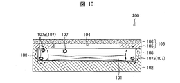
- FIG. 10 is a cross-sectional view showing a schematic configuration of an optical device package 200 according to the prior art.
- An optical device package 200 shown in FIG. 10 includes an optical device 101, a housing 102 that houses the optical device 101, and a lid 103 that fits the housing 102.
- the lid portion 103 has a metal frame (light non-transmissive portion) 105 in which an opening 104 is formed, and an optical window portion 106 that closes the opening 104.
- the optical window 106 is, for example, a single glass or a glass non-transparent material such as a metal layer formed at and around the edge of the glass.
- the optical device package 200 is obtained by housing the optical device 101 in the housing 102 in a state filled with an inert gas (not shown) and hermetically sealing the optical device 101 with the housing 102 and the lid portion 103.
- JP 9-148469 A (published on June 6, 1997)”
- the foreign matter 107 may enter the housing 102 before the lid 102 covers the housing 102.
- a method of observing the inside of the housing 102 immediately before the housing 102 is covered and detecting and removing the foreign matter 107 that has entered the housing 102 can be considered.
- the back side 108 of the metal frame 105 is likely to be a blind spot during observation, and it is difficult to detect and remove the foreign substance 107 (that is, the foreign substance 107a) in this blind spot.
- the foreign matter 107 that has entered the housing 102 adheres to or floats on the light receiving portion of the optical device 101 disposed on the upper surface of the optical device 101.
- the optical device 101 is an optical switching device
- crosstalk occurs due to light being refracted by the foreign matter 107, and this crosstalk causes malfunction of the optical device 101 in the optical device package 200.
- the optical device 101 is a solid-state imaging device
- there is a problem that the amount of received light is significantly reduced due to light being reflected or refracted by the foreign matter 107.
- the present invention has been made in view of the above-described problems, and an object of the present invention is to provide an optical device that is caused by foreign matter adhering to the light receiving portion of the optical device or floating of foreign matter on the light receiving portion.
- An object of the present invention is to provide an optical device package that can suppress malfunction or reduction in the amount of received light.
- an optical device package of the present invention includes an optical device, a housing that houses the optical device, a light non-transmissive portion that is formed of a light non-transmissive material and has an opening, and a light A lid portion made of a transparent material and having an optical window portion that closes the opening, and the light non-transmissive portion has at least one projecting portion projecting to the optical device side. It is characterized by.
- the protrusion prevents the foreign matter that enters the housing and remains on the side of the optical device from moving toward the light receiving portion of the optical device disposed on the upper surface of the optical device. it can. As a result, it is possible to prevent foreign matter from adhering to the light receiving portion of the optical device or from floating on the light receiving portion, so that it is possible to suppress malfunction of the optical device or reduction in the amount of received light. .
- the present invention it is possible to suppress the malfunction of the optical device or the decrease in the amount of received light caused by foreign matter adhering to the light receiving portion of the optical device or floating of foreign matter on the light receiving portion.
- FIG. 3 is an exploded perspective view of the optical device package according to Embodiment 1 of the present invention, and a perspective view showing a surface on the optical device side in the light non-transmissive portion.
- FIG. 2 is a cross-sectional view of the optical device package shown in FIG. (A)-(d) is sectional drawing of the optical device package which concerns on the 1st modification of Embodiment 1 of this invention, respectively.
- (A) And (b) is a top view which shows the surface by the side of the optical device in the light non-transmissive part based on the 2nd modification of Embodiment 1 of this invention, respectively. It is a disassembled perspective view of the optical device package which concerns on Embodiment 2 of this invention.
- FIG. 2 is a cross-sectional view of the optical device package shown in FIG. (A)-(d) is sectional drawing of the optical device package which concerns on the 1st modification of Embodiment 1 of this invention, respectively.
- (A) And (b)
- FIG. 6 is a cross-sectional view of the optical device package shown in FIG. (A)-(c) is sectional drawing of the optical device package which concerns on the modification of Embodiment 2 of this invention, respectively. It is sectional drawing which shows another example of the structure by which a protrusion part extends to the side wall side of a housing. It is sectional drawing which shows another example of the structure by which a protrusion part extends to the side wall side of a housing. It is sectional drawing which shows schematic structure of the optical device package which concerns on a prior art.
- the optical device package according to each embodiment described below is an optical device package in which an LCOS (Liquid Crystal On On Silicon) element is hermetically sealed, and is hereinafter referred to as an “LCOS package”.
- LCOS Liquid Crystal On On Silicon
- members having the same functions as those described above are denoted by the same reference numerals, and description thereof is omitted.
- FIG. 1 is an exploded perspective view of an LCOS (Liquid Crystal On Silicon) package 201 according to the first embodiment of the present invention.
- 2 is a cross-sectional view taken along line AA of the LCOS package 201 shown in FIG.
- FIG. 1 also shows a perspective view of the lid 3 provided in the LCOS package 201 as viewed from the back side.
- LCOS Liquid Crystal On Silicon
- An LCOS package (optical device package) 201 shown in FIGS. 1 and 2 includes an optical device unit 1, a housing 2, and a lid 3.
- the optical device unit 1 has an LCOS element (optical device) 11 and a heater 12.
- the LCOS element 11 includes a silicon substrate portion 11a and a liquid crystal portion 11b.
- the silicon substrate portion 11a is obtained by forming a drive circuit for driving the LCOS element 11 on a silicon substrate.
- the liquid crystal unit 11b is a light receiving portion of the LCOS element 11 provided on the upper surface of the LCOS element 11, and includes a transparent electrode, an alignment film, and the like in addition to the liquid crystal.
- the temperature of the LCOS element 11 needs to be precisely managed, and the heater 12 is responsible for controlling this temperature.
- the heater 12 can be omitted.
- the housing 2 accommodates the LCOS element 11 and has a ceramic substrate 21 and a sealing frame body 22.
- the sealing frame body 22 is a frame body provided on the ceramic substrate 21 so as to surround the LCOS element 11 and is made of light non-transmissive ceramic, metal, or the like.
- the lid 3 is provided above the LCOS element 11 and is a lid suitable for the housing 2.
- the lid 3 has a metal frame (light non-transmissive portion) 31 and a glass substrate (optical window portion) 32.
- the metal frame 31 is made of a non-permeable metal material, and an opening 33 is formed above the LCOS element 11. Then, the glass substrate 32 closes the opening 33. Thereby, light from the outside of the LCOS package 201 is transmitted through the glass substrate 32 and guided to the liquid crystal unit 11 b of the LCOS element 11.
- sealing frame body 22 and the metal frame 31 are joined together by a joining layer 41 made of solder or solder. Further, the edge and the vicinity thereof on the surface of the glass substrate 32 on the LCOS element 11 side are metallized, and this metallized portion is the metallized layer 42. Further, the metal frame 31 and the metallized layer 42 are joined by a joining layer 43 made of solder.
- the metal frame 31 has a protrusion 34 formed thereon.
- the protrusion 34 protrudes toward the LCOS element 11 on the surface of the metal frame 31 on the LCOS element 11 side.
- the distance between the silicon substrate portion 11a and the metal frame 31 can be reduced by the protruding portion 34.
- foreign matter that enters the housing 2 and remains on the side of the LCOS element 11 is prevented from moving toward the liquid crystal part 11b (light receiving part) of the LCOS element 11 disposed on the upper surface of the LCOS element 11. be able to.
- foreign matter can be prevented from adhering to the liquid crystal portion 11b of the LCOS element 11 or from floating on the liquid crystal portion 11b, so that malfunction of the LCOS element 11 can be suppressed.
- the protrusion 34 and the LCOS element 11 are separated from each other. Since the protrusion 34 and the LCOS element 11 are separated from each other, it is possible to prevent the protrusion 34 from coming into contact with the LCOS element 11 or pressing the LCOS element 11. Therefore, it is possible to prevent the LCOS element 11 from being damaged or malfunctioning due to the contact or pressure of the protrusion 34.
- the foreign matter having a size larger than the area corresponding to one pixel in the optical device is directly caused by the malfunction of the optical device or the decrease in the amount of received light. It is easy to cause.
- the separation distance between the protrusion 34 and the optical device having the pixel structure is preferably less than the pixel size of the optical device.
- the separation distance is preferably less than 10 ⁇ m.
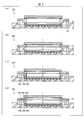
- 3A to 3D are cross-sectional views of LCOS packages 202 to 205 according to a first modification of the LCOS package 201, respectively.
- 3A is different from the LCOS package 201 in that the protrusion 34 and the sealing frame (side wall of the housing) 22 are separated from each other.
- Other configurations of the LCOS package 202 are the same as the configurations of the LCOS package 201.
- protruding portion 34 and the sealing frame body 22 are separated from each other, a margin for manufacturing tolerance of the protruding portion 34 can be ensured between the protruding portion 34 and the sealing frame body 22. In addition, foreign matter can be captured between the protruding portion 34 and the sealing frame body 22.
- the LCOS package 203 shown in FIG. 3B is different from the LCOS package 201 in the following points. Other configurations of the LCOS package 203 are the same as those of the LCOS package 201.
- the LCOS package 203 is provided with a protrusion 35 having a function similar to that of the protrusion 34 as a separate member from the metal frame 31 instead of the protrusion 34.
- the material of the protrusion part 35 is low outgas, and should just be a thing suitable for a general airtight sealing package, A metal, an epoxy resin, or an acrylic resin etc. are mentioned. Thereby, compared with the case where the metal frame 31 which has the protrusion part 34 is integrally molded, processing cost can be suppressed and the freedom degree of the shape of a protrusion part can be raised.
- the protruding portion 35 extends from directly above the LCOS element 11 to the side of the LCOS element 11. As a result, the distance from the side of the LCOS element 11 to the liquid crystal part 11b can be increased, so that the foreign substance directly causing the malfunction of the LCOS element 11 is directed toward the liquid crystal part 11b. Can be effectively suppressed.
- FIGS. 8 and 9 can be considered in addition to the example of FIG.
- FIG. 8 shows an LCOS package 210 in which the protruding portion 35 is shortened with respect to the LCOS package 203 (the tip of the protruding portion 35 is positioned immediately above the LCOS element 11).
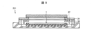
- FIG. 9 shows an LCOS package 211 in which protrusions 35 are formed in a step shape with respect to the LCOS package 203. Both the LCOS packages 210 and 211 can capture foreign substances in their respective gaps 37.
- the LCOS package 204 shown in FIG. 3C is different from the LCOS package 203 in the following points. Other configurations of the LCOS package 204 are the same as those of the LCOS package 203.
- the LCOS package 204 is provided with a plurality of protrusions 35.
- the protrusion 35 a provided closest to the LCOS element 11 extends toward the upper surface of the LCOS element 11.
- the protrusion 35 c provided on the side farthest from the LCOS element 11 extends toward the side of the LCOS element 11.
- the protrusions 35 b provided between the protrusions 35 a and 35 c extend toward the upper surface and the side of the LCOS element 11.
- the plurality of protrusions 35 it is possible to more reliably prevent foreign matters from adhering to the liquid crystal portion 11b of the LCOS element 11 or foreign matters from floating on the liquid crystal portion 11b. That is, it is difficult to freely control how the foreign object moves, but by providing a plurality of protrusions 35, it is possible to capture and hold the foreign object between the two protrusions 35. It becomes. As a result, it is possible to suppress the foreign matter from moving to above the liquid crystal part 11b.
- the LCOS package 205 shown in FIG. 3D is different from the LCOS package 204 in the following points. Other configurations of the LCOS package 205 are the same as those of the LCOS package 204.
- grooves 36a to 36c corresponding to the protruding portions 35a to 35c are formed on the metal frame 31 in a one-to-one relationship. Projections 35a to 35c are fitted into the grooves 36a to 36c, respectively.
- the height of the protruding portions 35a to 35c is set according to the depth of fitting the protruding portions 35a to 35c into the grooves 36a to 36c. Can be adjusted. As a result, a margin for manufacturing tolerances of the protrusions 35a to 35c can be ensured between the protrusions 35a to 35c and the LCOS element 11.
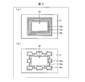
- FIGS. 4A and 4B are plan views each showing a surface of the metal frame 31 on the LCOS element 11 side according to a second modification of the present embodiment.
- the combination of the metal frame 31 and the protruding portion 35 will be described, but the same applies to the combination of the metal frame 31 and the protruding portion 34.
- 4A and 4B are provided with protrusions 35a to 35c (see FIGS. 3C and 3D).
- each of the protrusions 35a to 35c is provided in a frame shape and continuously so as to surround the opening 33 of the metal frame 31. For this reason, it can suppress that a foreign material moves toward the liquid crystal part 11b over the perimeter of the LCOS element 11.
- FIG. 4B each of the protrusions 35a to 35c is provided in a frame shape and intermittently so as to surround the opening 33 of the metal frame 31. According to the configuration of the metal frame 31 shown in FIG. 4B, when the protrusions 35a to 35c and the metal frame 31 are made of different materials, the stress generated in the metal frame 31 can be suppressed.
- the optical device housed in the optical device package according to the present invention may be an optical device that receives light or outputs light, and may be, for example, a MEMS (Micro Electro Mechanical System) mirror. Good. Further, this optical device may be a solid-state imaging device.
- the configuration of the optical device package according to the present invention relates to a decrease in the amount of light received in the optical device instead of the effect related to the malfunction of the optical device. You can enjoy the effect.
- the metallized layer 42 is formed on the glass substrate 32, but the metallized layer 42 may be omitted.
- a light non-transmissive material such as a metal layer may be formed on the edge of the glass and in the vicinity thereof.
- the separation distance between the LCOS element 11 and the protrusion 34 is smaller, the effect of suppressing the movement of the foreign matter is increased, while the possibility that the protrusion 34 contacts and / or presses the LCOS element 11 increases.
- the protruding portion 35 is about 100 ⁇ m, a certain degree of the suppression effect can be expected. The same applies to the protruding portion 35.
- the form in which the protrusions 34 are provided is clearly distinguished from the form in which the protrusions 35 are provided in order to simplify the description. Both forms can be applied.
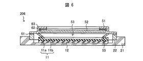
- FIG. 5 is an exploded perspective view of the LCOS package 206 according to the second embodiment of the present invention. 6 is a cross-sectional view of the LCOS package 206 shown in FIG.
- the LCOS package 206 shown in FIGS. 5 and 6 is different from the LCOS package 201 in that the lid 5 is provided instead of the lid 3.
- Other configurations of the LCOS package 206 are the same as those of the LCOS package 201.
- the lid 5 is provided above the LCOS element 11 and is a lid suitable for the housing 2.
- the lid 5 has a metal frame (light non-transmissive part) 51, a glass substrate (optical window part) 52, and a protruding part (light non-transmissive part) 55.
- the metal frame 51 is made of a light-impermeable metal material, and an opening 53 is formed above the LCOS element 11. Then, the glass substrate 52 closes the opening 53. Thereby, light from the outside of the LCOS package 206 is transmitted through the glass substrate 52 and guided to the liquid crystal unit 11 b of the LCOS element 11.
- sealing frame body 22 and the metal frame 51 are bonded together by a bonding layer 61 made of solder or solder. Further, the edge and the vicinity thereof on the surface of the glass substrate 52 opposite to the LCOS element 11 are metallized, and this metallized portion is the metallized layer 62. Furthermore, the metal frame 51 and the metallized layer 62 are joined together by a joining layer 63 made of solder.
- the materials of the metal frame 51 and the glass substrate 52 are the same as those of the metal frame 31 and the glass substrate 32, respectively.
- the metal frame 51 is provided with a protrusion 55 as a separate member from the metal frame 51.
- the protruding portion 55 protrudes from the surface of the metal frame 51 on the LCOS element 11 side to the LCOS element 11 side.
- the protrusion 55 can obtain the same effect of suppressing the movement of foreign matter as the protrusions 34 and 35.
- the glass substrate 52 is bonded to the surface of the metal frame 51 facing the LCOS element 11 (that is, the LCOS element 11 side). Thereby, since the edge of the glass substrate 52 is not exposed to the outside of the LCOS package 206, damage from the outside of the LCOS package 206 to the glass substrate 52 can be reduced.
- Modification of Embodiment 2 7A to 7C are cross-sectional views of LCOS packages 207 to 209 according to modifications of the LCOS package 206, respectively.
- the LCOS packages 207 to 209 shown in FIGS. 7A to 7C are different from the LCOS package 206 in the following points. Other configurations of the LCOS packages 207 to 209 are the same as the configuration of the LCOS package 206.
- the protrusions 55 of the LCOS package 206 shown in FIG. 6 are provided with diagonal lines in the cross section of FIG. 6, but the protrusions 55 of the LCOS packages 207 to 209 are respectively shown in FIGS. Is provided in an L shape in the cross section.
- the distance between the glass substrate 52 and the protruding portion 55 is smaller than the LCOS package 207 shown in FIG.
- the LCOS package 209 shown in FIG. 7C has a smaller distance between the sealing frame body 22 and the tip of the protruding portion 55 than the LCOS package 208 shown in FIG. 7B. Yes.
- An optical device package of the present invention includes an optical device, a housing for housing the optical device, a light non-transmissive portion made of a light non-transmissive material and having an opening formed therein, and a light transmissive material for closing the opening.
- a lid portion having an optical window portion, and the light non-transmissive portion has at least one projecting portion projecting toward the optical device.
- the protrusion prevents the foreign matter that enters the housing and remains on the side of the optical device from moving toward the light receiving portion of the optical device disposed on the upper surface of the optical device. it can. As a result, it is possible to prevent foreign matter from adhering to the light receiving portion of the optical device or from floating on the light receiving portion, so that it is possible to suppress malfunction of the optical device or reduction in the amount of received light. .
- the optical device package of the present invention at least one of the protrusions and the optical device are separated from each other.
- the protruding portion and the optical device are separated from each other, it is possible to prevent the protruding portion from contacting the optical device or pressing the optical device. Therefore, it is possible to prevent the optical device from being damaged, malfunctioning, or reducing the amount of received light due to the contact or compression of the protrusion.
- the separation distance between the at least one protrusion and the optical device is less than the pixel size of the optical device.
- At least one of the protrusions and the side wall of the housing are separated from each other.
- the protruding portion and the side wall of the housing are separated from each other, a margin for manufacturing tolerance of the protruding portion can be ensured between the protruding portion and the side wall of the housing. Moreover, according to said structure, it becomes possible to capture a foreign material between a protrusion part and the side wall of a housing.
- the optical device package of the present invention extends so that at least a part of the at least one projecting portion approaches the side wall of the housing as it approaches the tip of the projecting portion.
- the foreign matter can be captured on the side wall side of the housing in the protruding portion.
- At least one of the protrusions extends to the side of the optical device.
- the light non-transmissive portion has a plurality of the protruding portions.
- At least one of the protrusions is a member that is attached to the light non-transmission part and is separate from the light non-transmission part.
- the processing cost can be reduced and the degree of freedom of the shape of the protruding portion can be increased as compared with the case where the light non-transmitting portion having the protruding portion is integrally formed.
- At least one of the protruding portions is a member separate from the light non-transmissive portion, which is fitted in a groove formed in the light non-transmissive portion.
- the height of the protruding portion can be adjusted according to the depth of fitting the protruding portion into the groove formed in the light non-transmitting portion. Therefore, it is possible to ensure a margin for manufacturing tolerances of the protruding portion between the protruding portion and the optical device.
- the optical window portion is bonded to a surface of the light non-transmissive portion facing the optical device.
- the present invention can be used for an optical device package in which an optical device is hermetically sealed.
- the present invention is a light comprising a light non-transmission part made of a light non-transmission material and having an opening and an optical window part made of a light transmission material and closing the opening.
- Optical Device Unit 2 Housing 3 Lid 5 Lid 11 LCOS Element (Optical Device) 22 Sealing frame (side wall of housing) 31 Metal frame (light non-transmission part) 32 Glass substrate (optical window) 33 Openings 34 and 35 Protruding part (light non-transmitting part) 35a to 35c Projection (light non-transmission part) 51 Metal frame (light non-transmissive part) 52 Glass substrate (optical window) 53 Opening 55 Protruding part (light non-transmitting part) 201 to 211 LCOS package (optical device package)
Landscapes
- Physics & Mathematics (AREA)
- Nonlinear Science (AREA)
- Optics & Photonics (AREA)
- Crystallography & Structural Chemistry (AREA)
- Chemical & Material Sciences (AREA)
- General Physics & Mathematics (AREA)
- Mathematical Physics (AREA)
- Engineering & Computer Science (AREA)
- Microelectronics & Electronic Packaging (AREA)
- Light Receiving Elements (AREA)
- Solid State Image Pick-Up Elements (AREA)
- Liquid Crystal (AREA)
- Packaging Frangible Articles (AREA)
Abstract
光デバイスの受光部分に異物が付着する、もしくはこの受光部分上を異物が浮遊することに起因する、光デバイスの誤動作または受光量の低下を抑制する。金属フレーム(31)は、LCOS素子(11)の側に突出する突出部(34)を少なくとも1つ有している。
Description
本発明は、光デバイスを気密封止してなる光デバイスパッケージに関するものである。特に、本発明は、光非透過性材料からなり、開口が形成されている光非透過部と、光透過性材料からなり、上記開口を塞ぐ光学窓部と、を有する蓋部を備えた光デバイスパッケージに関するものである。
従来、光デバイスに対する湿度等の影響を抑制するための技術として、光デバイスを気密封止してなる光デバイスパッケージが知られている。特に、光非透過性材料からなり、開口が形成されている光非透過部と、光透過性材料からなり、上記開口を塞ぐ光学窓部と、を有する蓋部を備えた光デバイスパッケージが知られている(特許文献1参照)。
図10は、従来技術に係る光デバイスパッケージ200の概略構成を示す断面図である。図10に示す光デバイスパッケージ200は、光デバイス101、光デバイス101を収納するハウジング102、およびハウジング102に適合する蓋部103を備えている。蓋部103は、開口104が形成されている金属フレーム(光非透過部)105、およびこの開口104を塞ぐ光学窓部106を有している。光学窓部106は例えば、ガラス単体、もしくは、ガラスの縁およびその近傍に金属層等の光非透過性材料を形成したものである。
また、光デバイスパッケージ200は、不活性ガス(図示しない)を充填した状態で光デバイス101をハウジング102に収納して、ハウジング102および蓋部103によって光デバイス101を気密封止したものである。
図10に示す光デバイスパッケージ200では、蓋部103によってハウジング102に蓋をする前に、ハウジング102内に異物107が入り込む虞がある。
従来、ハウジング102内に異物107が入り込むことを避けるため、クリーンルームにて光デバイスパッケージ200を製造する等の手法が採られてきた。しかしながら、このような手法を用いたとしても、ハウジング102内に異物107が入り込むことを完全に防ぐことは難しい。
また、ハウジング102に蓋をする直前に、ハウジング102内を観察して、ハウジング102内に入り込んだ異物107を検出および除去するという手法も考えられる。しかしながら、この手法においては、観察に際して金属フレーム105の裏側108等が死角となりやすく、この死角にある異物107(すなわち、異物107a)を検出および除去することは難しい。
この結果、図10に示す光デバイスパッケージ200では、ハウジング102内に入り込んだ異物107が、光デバイス101の上面に配置された光デバイス101の受光部分に付着する、もしくはこの受光部分上を浮遊する虞がある。そしてこれにより、光デバイス101が光スイッチングデバイスである場合、異物107にて光が屈折されることでクロストークが発生し、このクロストークによって、光デバイスパッケージ200では、光デバイス101の誤動作が生じるという問題が発生する。また、光デバイス101が固体撮像素子である場合、異物107にて光が反射または屈折されることで受光量が著しく低下するという問題が発生する。
本発明は、上記の課題に鑑みて為されたものであり、その目的は、光デバイスの受光部分に異物が付着する、もしくはこの受光部分上を異物が浮遊することに起因する、光デバイスの誤動作または受光量の低下を抑制することを可能とする光デバイスパッケージを提供することにある。
上記の課題を解決するために、本発明の光デバイスパッケージは、光デバイスと、上記光デバイスを収納するハウジングと、光非透過性材料からなり開口が形成されている光非透過部と、光透過性材料からなり上記開口を塞ぐ光学窓部とを有する蓋部と、を備えており、上記光非透過部は、上記光デバイスの側に突出する突出部を少なくとも1つ有していることを特徴としている。
上記の構成によれば、ハウジング内に入り込み光デバイスの側方に残留した異物が、光デバイスの上面に配置された光デバイスの受光部分に向けて移動することを、突出部により抑制することができる。これにより、光デバイスの受光部分に異物が付着する、もしくはこの受光部分上を異物が浮遊することを防止することができるので、光デバイスの誤動作または受光量の低下を抑制することが可能となる。
本発明によれば、光デバイスの受光部分に異物が付着する、もしくはこの受光部分上を異物が浮遊することに起因する、光デバイスの誤動作または受光量の低下を抑制することが可能となる。
本発明を実施するための形態について、以下に説明する。なお、以下に説明する各実施の形態に係る光デバイスパッケージは、LCOS(Liquid Crystal On Silicon)素子を気密封止してなる光デバイスパッケージなので、以下ではこれを「LCOSパッケージ」という。また、以下、先に説明した部材と同じ機能を有する部材については、同じ符号を付記し、その説明を省略する。
〔実施の形態1〕
図1は、本発明の第1の実施の形態に係るLCOS(Liquid Crystal On Silicon)パッケージ201の分解斜視図である。また、図2は、図1に示すLCOSパッケージ201のA-A線矢視断面図である。なお、図1には、LCOSパッケージ201が備える蓋部3を裏面側から見た斜視図を併せて示している。
図1は、本発明の第1の実施の形態に係るLCOS(Liquid Crystal On Silicon)パッケージ201の分解斜視図である。また、図2は、図1に示すLCOSパッケージ201のA-A線矢視断面図である。なお、図1には、LCOSパッケージ201が備える蓋部3を裏面側から見た斜視図を併せて示している。
図1および図2に示すLCOSパッケージ(光デバイスパッケージ)201は、光デバイスユニット1、ハウジング2、および蓋部3を備えている。
光デバイスユニット1は、LCOS素子(光デバイス)11およびヒーター12を有している。また、LCOS素子11は、シリコン基板部11aおよび液晶部11bを有している。シリコン基板部11aは、LCOS素子11を駆動するための駆動回路をシリコン基板に形成したものである。液晶部11bは、LCOS素子11の上面に設けられたLCOS素子11の受光部分であり、液晶に加え、透明電極、配向膜等を有している。また、LCOS素子11は、その温度が精緻に管理される必要があり、この温度の制御をヒーター12が担っている。なお、LCOS素子11のかわりに固体撮像素子を用いる場合、ヒーター12を省略することができる。
ハウジング2は、LCOS素子11を収納するものであり、セラミック基板21および封止枠体22を有している。封止枠体22は、LCOS素子11を囲むようにセラミック基板21上に設けられた枠体であり、光非透過性のセラミック、金属等からなる。
蓋部3は、LCOS素子11の上方に設けられており、ハウジング2に適合する蓋部である。蓋部3は、金属フレーム(光非透過部)31およびガラス基板(光学窓部)32を有している。
金属フレーム31は、非透過性の金属材料からなり、LCOS素子11の上方に開口33が形成されている。そして、ガラス基板32は開口33を塞ぐ。これにより、LCOSパッケージ201外部からの光は、ガラス基板32を透過して、LCOS素子11の液晶部11bに導かれる。
なお、封止枠体22と金属フレーム31とは、ハンダまたはロウからなる接合層41によって接合されている。また、ガラス基板32におけるLCOS素子11側の面における縁およびその近傍はメタライズされており、このメタライズされている部分がメタライズ層42である。さらに、金属フレーム31とメタライズ層42とは、ハンダからなる接合層43によって接合されている。
ここで、金属フレーム31には、突出部34が形成されている。突出部34は、金属フレーム31におけるLCOS素子11側の面において、LCOS素子11の側に突出している。
突出部34により、シリコン基板部11aと金属フレーム31との間隔を小さくことができる。そしてこれにより、ハウジング2内に入り込みLCOS素子11の側方に残留した異物が、LCOS素子11の上面に配置されたLCOS素子11の液晶部11b(受光部分)に向けて移動することを抑制することができる。これにより、LCOS素子11の液晶部11bに異物が付着する、もしくはこの液晶部11b上を異物が浮遊することを防止することができるので、LCOS素子11の誤動作を抑制することが可能となる。
また、突出部34と、LCOS素子11とが離間されている。突出部34とLCOS素子11とが離間されているため、突出部34がLCOS素子11と接触したり、LCOS素子11を圧迫したりすることを防ぐことができる。従って、突出部34の接触または圧迫によって、LCOS素子11が損傷したり誤動作したりすることを防ぐことができる。
ところで、LCOS素子11をはじめとする、画素構造を有する光デバイスでは総じて、この光デバイスにおける1画素に相当する面積以上のサイズを有する異物は、この光デバイスの誤動作または受光量の低下の直接的な原因となりやすい。
この場合、突出部34と、上記画素構造を有する光デバイスとの離間距離は、この光デバイスの画素サイズ未満であることが好ましい。例えば、この光デバイスの1ピクセルが10μm角である場合、10μm×10μm以上のサイズの異物が上記原因となり得るので、この場合、上記離間距離は10μm未満であることが好ましい。
これにより、上記画素構造を有する光デバイスの誤動作または受光量の低下の直接的な原因となる異物が、この光デバイスの受光部分に向けて移動することを効果的に抑制することができる。
(実施の形態1の第1変形例)
図3の(a)~(d)はそれぞれ、LCOSパッケージ201の第1変形例に係るLCOSパッケージ202~205の断面図である。
図3の(a)~(d)はそれぞれ、LCOSパッケージ201の第1変形例に係るLCOSパッケージ202~205の断面図である。
図3の(a)に示すLCOSパッケージ202は、突出部34と、封止枠体(ハウジングの側壁)22とが離間されている点が、LCOSパッケージ201と異なっている。LCOSパッケージ202のその他の構成は、LCOSパッケージ201の構成と同様である。
突出部34と封止枠体22とが離間されているため、突出部34と封止枠体22との間において、突出部34の製造公差に対するマージンを確保することができる。また、突出部34と封止枠体22との間にて、異物を捕捉することが可能となる。
図3の(b)に示すLCOSパッケージ203は、下記の点が、LCOSパッケージ201と異なっている。LCOSパッケージ203のその他の構成は、LCOSパッケージ201の構成と同様である。
LCOSパッケージ203には、突出部34の替わりに、突出部34と同様の機能を有する突出部35が、金属フレーム31と別部材として設けられている。なお、突出部35の材質は、低アウトガスであり、一般的な気密封止パッケージに適したものであればよく、金属、エポキシ樹脂、またはアクリル樹脂等が挙げられる。これにより、突出部34を有する金属フレーム31を一体成形する場合と比べて、加工コストを抑え、突出部の形状の自由度を上げることができる。
また、LCOSパッケージ203において、突出部35は、LCOS素子11の直上から、LCOS素子11の側方にまで延びている。これにより、異物がLCOS素子11の側方から液晶部11b上に到達するまでの距離を長くとることができるため、LCOS素子11の誤動作の直接的な原因となる異物が、液晶部11bに向けて移動することを効果的に抑制することができる。
さらに、突出部35は、その一部または全部が、突出部35の先端に近づく程封止枠体22に近づくように延びており、これにより、突出部35における封止枠体22側にて、異物を捕捉することが可能となる。この構成については、図3の(b)の例の他、図8および9の例も考えられる。図8は、LCOSパッケージ203に対して、突出部35を短くした(突出部35の先端がLCOS素子11の直上に位置する)LCOSパッケージ210である。図9は、LCOSパッケージ203に対して、突出部35を段型に形成したLCOSパッケージ211である。LCOSパッケージ210および211共に、それら各々の隙間37にて、異物を捕捉することができる。
図3の(c)に示すLCOSパッケージ204は、下記の点が、LCOSパッケージ203と異なっている。LCOSパッケージ204のその他の構成は、LCOSパッケージ203の構成と同様である。
LCOSパッケージ204には、突出部35が複数設けられている。突出部35のうち、最もLCOS素子11側に設けられた突出部35aは、LCOS素子11の上面に向けて延びている。突出部35のうち、最もLCOS素子11から遠い側に設けられた突出部35cは、LCOS素子11の側方に向けて延びている。突出部35のうち、突出部35aと突出部35cとの間に設けられた突出部35bは、LCOS素子11の上面および側方に向けて延びている。
複数の突出部35を設けることにより、LCOS素子11の液晶部11bに異物が付着する、もしくはこの液晶部11b上を異物が浮遊することを、より確実に防止することができる。すなわち、異物がどのように移動するかを自在に制御することは困難であるが、複数の突出部35を設けることにより、異物を2つの突出部35間にて捕捉して留まらせることが可能となる。結果として異物が液晶部11bの上方にまで移動することを抑制することができる。
図3の(d)に示すLCOSパッケージ205は、下記の点が、LCOSパッケージ204と異なっている。LCOSパッケージ205のその他の構成は、LCOSパッケージ204の構成と同様である。
LCOSパッケージ205は、金属フレーム31に、突出部35a~35cと1対1に対応する溝36a~36cが形成されている。溝36a~36cには、それぞれ、突出部35a~35cが嵌め込まれる。
溝36a~36cに、それぞれ、突出部35a~35cが嵌め込まれる構造とすることによって、溝36a~36cに突出部35a~35cを嵌め込む深さに応じて、突出部35a~35cの高さを調整することができる。これにより、突出部35a~35cとLCOS素子11との間において、突出部35a~35cの製造公差に対するマージンを確保することができる。
(実施の形態1の第2変形例)
図4の(a)および(b)はそれぞれ、本実施の形態の第2変形例に係る、金属フレーム31におけるLCOS素子11側の面を示す平面図である。ここでは、金属フレーム31および突出部35の組み合わせについて説明を行うが、金属フレーム31および突出部34の組み合わせについても同様である。
図4の(a)および(b)はそれぞれ、本実施の形態の第2変形例に係る、金属フレーム31におけるLCOS素子11側の面を示す平面図である。ここでは、金属フレーム31および突出部35の組み合わせについて説明を行うが、金属フレーム31および突出部34の組み合わせについても同様である。
図4の(a)および(b)のそれぞれに示す金属フレーム31には、突出部35a~35c(図3の(c)および(d)参照)が設けられている。
図4の(a)に示す金属フレーム31において、突出部35a~35cの各々は、金属フレーム31の開口33を囲むように、枠状かつ連続的に設けられている。このため、LCOS素子11の全周に亘って、異物が液晶部11bに向けて移動することを抑制することができる。一方、図4の(b)に示す金属フレーム31において、突出部35a~35cの各々は、金属フレーム31の開口33を囲むように、枠状かつ断続的に設けられている。図4の(b)に示す金属フレーム31の構成によれば、突出部35a~35cと金属フレーム31とが異なる材料であった場合、金属フレーム31に生じる応力を抑制することができる。
(付記事項)
本実施の形態では、LCOS素子を収納した光デバイスパッケージ(LCOSパッケージ)について説明したが、本発明は、これに限定されない。すなわち、本発明に係る光デバイスパッケージに収納される光デバイスは、光が入力される、又は、光を出力する光デバイスであればよく、例えば、MEMS(Micro Electro Mechanical System)ミラーであってもよい。また、この光デバイスは、固体撮像素子であってもよく、この場合、本発明に係る光デバイスパッケージの構成により、光デバイスの誤動作に係る効果に替えて、光デバイスにおける受光量の低下に係る効果を享受することができる。
本実施の形態では、LCOS素子を収納した光デバイスパッケージ(LCOSパッケージ)について説明したが、本発明は、これに限定されない。すなわち、本発明に係る光デバイスパッケージに収納される光デバイスは、光が入力される、又は、光を出力する光デバイスであればよく、例えば、MEMS(Micro Electro Mechanical System)ミラーであってもよい。また、この光デバイスは、固体撮像素子であってもよく、この場合、本発明に係る光デバイスパッケージの構成により、光デバイスの誤動作に係る効果に替えて、光デバイスにおける受光量の低下に係る効果を享受することができる。
また、上述したとおり、ガラス基板32にはメタライズ層42が形成されているが、このメタライズ層42は省略されてもよい。換言すれば、光学窓部がガラス(光透過性材料)単体でさえあれば、このガラスの縁およびその近傍に金属層等の光非透過性材料を形成したものであってもよい。
また、LCOS素子11と突出部34との離間距離が小さい程、異物の移動の抑制効果が高まる一方、突出部34がLCOS素子11を接触および/または圧迫する虞が高まる。突出部34がLCOS素子11を接触または圧迫する虞をできるだけ低減したい場合、LCOS素子11と突出部34との離間距離を100μm程度としても、ある程度の上記抑制効果が見込める。突出部35についても同様である。
さらに、LCOSパッケージ201~205では、説明を簡潔にするために、突出部34を設ける形態と突出部35を設ける形態とを明確に区別したが、実際は、LCOSパッケージ201~205の全てにおいてこれらの両形態を適用することが可能である。
〔実施の形態2〕
図5は、本発明の第2の実施の形態に係るLCOSパッケージ206の分解斜視図である。また、図6は、図5に示すLCOSパッケージ206のB-B線矢視断面図である。
図5は、本発明の第2の実施の形態に係るLCOSパッケージ206の分解斜視図である。また、図6は、図5に示すLCOSパッケージ206のB-B線矢視断面図である。
図5および図6に示すLCOSパッケージ206は、蓋部3の替わりに蓋部5を備えている点が、LCOSパッケージ201と異なっている。LCOSパッケージ206のその他の構成は、LCOSパッケージ201の構成と同様である。
蓋部5は、LCOS素子11の上方に設けられており、ハウジング2に適合する蓋部である。蓋部5は、金属フレーム(光非透過部)51、ガラス基板(光学窓部)52、および突出部(光非透過部)55を有している。
金属フレーム51は、光非透過性の金属材料からなり、LCOS素子11の上方に開口53が形成されている。そして、ガラス基板52は開口53を塞ぐ。これにより、LCOSパッケージ206外部からの光は、ガラス基板52を透過して、LCOS素子11の液晶部11bに導かれる。
なお、封止枠体22と金属フレーム51とは、ハンダまたはロウからなる接合層61によって接合されている。また、ガラス基板52におけるLCOS素子11と反対側の面における縁およびその近傍はメタライズされており、このメタライズされている部分がメタライズ層62である。さらに、金属フレーム51とメタライズ層62とは、ハンダからなる接合層63によって接合されている。
金属フレーム51およびガラス基板52の材質は、それぞれ、金属フレーム31およびガラス基板32の材質と同じである。
金属フレーム51は、突出部55が、金属フレーム51と別部材として設けられている。突出部55は、金属フレーム51におけるLCOS素子11側の面から、LCOS素子11の側に突出している。突出部55によっても、突出部34および35と同様の、異物の移動の抑制効果を得ることができる。
LCOSパッケージ206において、ガラス基板52は、金属フレーム51におけるLCOS素子11と対向する面(すなわち、LCOS素子11側)に接合されている。これにより、ガラス基板52の縁がLCOSパッケージ206の外部に露出しないので、ガラス基板52に対するLCOSパッケージ206の外部からのダメージを低減することができる。
(実施の形態2の変形例)
図7の(a)~(c)はそれぞれ、LCOSパッケージ206の変形例に係るLCOSパッケージ207~209の断面図である。
図7の(a)~(c)はそれぞれ、LCOSパッケージ206の変形例に係るLCOSパッケージ207~209の断面図である。
図7の(a)~(c)にそれぞれ示すLCOSパッケージ207~209は、下記の点が、LCOSパッケージ206と異なっている。LCOSパッケージ207~209のその他の構成は、LCOSパッケージ206の構成と同様である。
図6に示すLCOSパッケージ206の突出部55は、図6の断面において斜線状に設けられていたが、LCOSパッケージ207~209の突出部55は、それぞれ、図7の(a)~(c)の断面においてL字形に設けられている。
図7の(b)に示すLCOSパッケージ208は、図7の(a)に示すLCOSパッケージ207と比較して、ガラス基板52と突出部55との間隔が小さくなっている。また、図7の(c)に示すLCOSパッケージ209は、図7の(b)に示すLCOSパッケージ208と比較して、封止枠体22と突出部55の先端との離間距離が小さくなっている。
〔まとめ〕
本発明は、以下のように解釈することもできる。
本発明は、以下のように解釈することもできる。
本発明の光デバイスパッケージは、光デバイスと、上記光デバイスを収納するハウジングと、光非透過性材料からなり開口が形成されている光非透過部と、光透過性材料からなり上記開口を塞ぐ光学窓部とを有する蓋部と、を備えており、上記光非透過部は、上記光デバイスの側に突出する突出部を少なくとも1つ有している。
上記の構成によれば、ハウジング内に入り込み光デバイスの側方に残留した異物が、光デバイスの上面に配置された光デバイスの受光部分に向けて移動することを、突出部により抑制することができる。これにより、光デバイスの受光部分に異物が付着する、もしくはこの受光部分上を異物が浮遊することを防止することができるので、光デバイスの誤動作または受光量の低下を抑制することが可能となる。
また、本発明の光デバイスパッケージは、少なくとも1つの上記突出部と、上記光デバイスとが離間されている。
上記の構成によれば、突出部と光デバイスとが離間されているため、突出部が光デバイスと接触したり、光デバイスを圧迫したりすることを防ぐことができる。従って、突出部の接触または圧迫によって、光デバイスが損傷したり誤動作または受光量の低下を生じたりすることを防ぐことができる。
ところで、光デバイスが画素構造を有するものである場合、1画素に相当する面積以上のサイズを有する異物は、誤動作または受光量の低下の直接的な原因となりやすい。
この場合、上記少なくとも1つの突出部と、上記光デバイスとの離間距離は、上記光デバイスの画素サイズ未満である。
上記の構成によれば、光デバイスの誤動作または受光量の低下の直接的な原因となる異物が、光デバイスの受光部分に向けて移動することを効果的に抑制することができる。
また、本発明の光デバイスパッケージは、少なくとも1つの上記突出部と、上記ハウジングの側壁とが離間されている。
上記の構成によれば、突出部とハウジングの側壁とが離間されているため、突出部とハウジングの側壁との間において、突出部の製造公差に対するマージンを確保することができる。また、上記の構成によれば、突出部とハウジングの側壁との間にて、異物を捕捉することが可能となる。
また、本発明の光デバイスパッケージは、上記少なくとも1つの突出部の少なくとも一部が、この突出部の先端に近づく程上記ハウジングの側壁に近づくように延びている。
上記の構成によれば、突出部におけるハウジングの側壁側にて、異物を捕捉することが可能となる。
また、本発明の光デバイスパッケージにおいて、少なくとも1つの上記突出部は、上記光デバイスの側方にまで延びている。
また、本発明の光デバイスパッケージにおいて、上記光非透過部は、上記突出部を複数有している。
上記の構成によれば、光デバイスの受光部分に異物が付着する、もしくはこの受光部分上を異物が浮遊することを、より確実に防止することができる。
また、本発明の光デバイスパッケージにおいて、少なくとも1つの上記突出部は、上記光非透過部に取り付けられた、上記光非透過部とは別体の部材である。
上記の構成によれば、突出部を有する光非透過部を一体成形する場合と比べて、加工コストを抑え、突出部の形状の自由度を上げることができる。
また、本発明の光デバイスパッケージにおいて、少なくとも1つの上記突出部は、上記光非透過部に形成された溝に嵌め込まれた、上記光非透過部とは別体の部材である。
上記の構成によれば、光非透過部に形成された溝に突出部を嵌め込む深さに応じて、突出部の高さを調整することができる。これにより、突出部と光デバイスとの間において、突出部の製造公差に対するマージンを確保することができる。
また、本発明の光デバイスパッケージにおいて、上記光学窓部は、上記光非透過部における上記光デバイスと対向する面に接合されている。
上記の構成によれば、光学窓部の縁が光デバイスパッケージの外部に露出しないので、光学窓部に対する光デバイスパッケージの外部からのダメージを低減することができる。
本発明は上述した各実施形態に限定されるものではなく、請求項に示した範囲で種々の変更が可能であり、異なる実施形態にそれぞれ開示された技術的手段を適宜組み合わせて得られる実施形態についても本発明の技術的範囲に含まれる。
本発明は、光デバイスを気密封止してなる光デバイスパッケージに利用することができる。特に、本発明は、光非透過性材料からなり、開口が形成されている光非透過部と、光透過性材料からなり、上記開口を塞ぐ光学窓部と、を有する蓋部を備えた光デバイスパッケージに利用することができる。
1 光デバイスユニット
2 ハウジング
3 蓋部
5 蓋部
11 LCOS素子(光デバイス)
22 封止枠体(ハウジングの側壁)
31 金属フレーム(光非透過部)
32 ガラス基板(光学窓部)
33 開口
34および35 突出部(光非透過部)
35a~35c 突出部(光非透過部)
51 金属フレーム(光非透過部)
52 ガラス基板(光学窓部)
53 開口
55 突出部(光非透過部)
201~211 LCOSパッケージ(光デバイスパッケージ)
2 ハウジング
3 蓋部
5 蓋部
11 LCOS素子(光デバイス)
22 封止枠体(ハウジングの側壁)
31 金属フレーム(光非透過部)
32 ガラス基板(光学窓部)
33 開口
34および35 突出部(光非透過部)
35a~35c 突出部(光非透過部)
51 金属フレーム(光非透過部)
52 ガラス基板(光学窓部)
53 開口
55 突出部(光非透過部)
201~211 LCOSパッケージ(光デバイスパッケージ)
Claims (10)
- 光デバイスと、
上記光デバイスを収納するハウジングと、
光非透過性材料からなり開口が形成されている光非透過部と、光透過性材料からなり上記開口を塞ぐ光学窓部とを有する蓋部と、を備えており、
上記光非透過部は、上記光デバイスの側に突出する突出部を少なくとも1つ有していることを特徴とする光デバイスパッケージ。 - 少なくとも1つの上記突出部と、上記光デバイスとが離間されていることを特徴とする請求項1に記載の光デバイスパッケージ。
- 上記光デバイスは、画素構造を有するものであり、
上記少なくとも1つの突出部と、上記光デバイスとの離間距離は、上記光デバイスの画素サイズ未満であることを特徴とする請求項2に記載の光デバイスパッケージ。 - 少なくとも1つの上記突出部と、上記ハウジングの側壁とが離間されていることを特徴とする請求項1から3のいずれか1項に記載の光デバイスパッケージ。
- 上記少なくとも1つの突出部の少なくとも一部が、この突出部の先端に近づく程上記ハウジングの側壁に近づくように延びていることを特徴とする請求項4に記載の光デバイスパッケージ。
- 少なくとも1つの上記突出部は、上記光デバイスの側方にまで延びていることを特徴とする請求項1から5のいずれか1項に記載の光デバイスパッケージ。
- 上記光非透過部は、上記突出部を複数有していることを特徴とする請求項1から6のいずれか1項に記載の光デバイスパッケージ。
- 少なくとも1つの上記突出部は、上記光非透過部に取り付けられた、上記光非透過部とは別体の部材であることを特徴とする請求項1から7のいずれか1項に記載の光デバイスパッケージ。
- 少なくとも1つの上記突出部は、上記光非透過部に形成された溝に嵌め込まれた、上記光非透過部とは別体の部材であることを特徴とする請求項8に記載の光デバイスパッケージ。
- 上記光学窓部は、上記光非透過部における上記光デバイスと対向する面に接合されていることを特徴とする請求項1から9のいずれか1項に記載の光デバイスパッケージ。
Priority Applications (2)
| Application Number | Priority Date | Filing Date | Title |
|---|---|---|---|
| CN201680002186.1A CN106796365A (zh) | 2015-04-17 | 2016-03-23 | 光器件封装体 |
| US15/501,258 US10007137B2 (en) | 2015-04-17 | 2016-03-23 | Optical device package |
Applications Claiming Priority (2)
| Application Number | Priority Date | Filing Date | Title |
|---|---|---|---|
| JP2015085405A JP2016206313A (ja) | 2015-04-17 | 2015-04-17 | 光デバイスパッケージ |
| JP2015-085405 | 2015-04-17 |
Publications (1)
| Publication Number | Publication Date |
|---|---|
| WO2016167093A1 true WO2016167093A1 (ja) | 2016-10-20 |
Family
ID=57126499
Family Applications (1)
| Application Number | Title | Priority Date | Filing Date |
|---|---|---|---|
| PCT/JP2016/059242 Ceased WO2016167093A1 (ja) | 2015-04-17 | 2016-03-23 | 光デバイスパッケージ |
Country Status (4)
| Country | Link |
|---|---|
| US (1) | US10007137B2 (ja) |
| JP (1) | JP2016206313A (ja) |
| CN (1) | CN106796365A (ja) |
| WO (1) | WO2016167093A1 (ja) |
Families Citing this family (5)
| Publication number | Priority date | Publication date | Assignee | Title |
|---|---|---|---|---|
| US10658255B2 (en) * | 2017-01-03 | 2020-05-19 | Advanced Semsconductor Engineering, Inc. | Semiconductor device package and a method of manufacturing the same |
| JP7181050B2 (ja) * | 2018-10-18 | 2022-11-30 | 浜松ホトニクス株式会社 | 放射線撮像装置 |
| JP7039450B2 (ja) * | 2018-12-25 | 2022-03-22 | 京セラ株式会社 | 光学装置用パッケージおよび光学装置ならびに光学装置の製造方法 |
| US11195864B2 (en) * | 2019-03-01 | 2021-12-07 | Omnivision Technologies, Inc. | Flip-chip sample imaging devices with self-aligning lid |
| CN115712221A (zh) * | 2021-08-23 | 2023-02-24 | 中强光电股份有限公司 | 光机模块 |
Citations (3)
| Publication number | Priority date | Publication date | Assignee | Title |
|---|---|---|---|---|
| JPH10214031A (ja) * | 1997-01-29 | 1998-08-11 | Tec Corp | Lcdカバー装置 |
| JP2004053964A (ja) * | 2002-07-19 | 2004-02-19 | Sony Corp | 液晶表示装置 |
| JP2013101218A (ja) * | 2011-11-08 | 2013-05-23 | Mitsubishi Electric Corp | 表示装置のフロントユニット |
Family Cites Families (10)
| Publication number | Priority date | Publication date | Assignee | Title |
|---|---|---|---|---|
| JP2581022B2 (ja) * | 1994-10-31 | 1997-02-12 | 日本電気株式会社 | 表示部付き電子機器の防塵構造 |
| JPH09148469A (ja) | 1995-11-17 | 1997-06-06 | Texas Instr Inc <Ti> | 光学的窓を備えたハーメチックパッケージおよびその方法 |
| JPH11352897A (ja) * | 1998-06-08 | 1999-12-24 | Mitsubishi Electric Corp | フラットパネルディスプレイ装置及びプラズマディスプレイ装置 |
| DE10031251A1 (de) * | 2000-06-27 | 2002-01-10 | Siemens Ag | Fronteinheit eines elektrischen Gerätes |
| US6683298B1 (en) * | 2000-11-20 | 2004-01-27 | Agilent Technologies Inc. | Image sensor packaging with package cavity sealed by the imaging optics |
| JP2003302620A (ja) * | 2002-04-09 | 2003-10-24 | Fuji Photo Film Co Ltd | 液晶表示装置 |
| JP2006041313A (ja) * | 2004-07-29 | 2006-02-09 | Kyocera Corp | 光半導体装置 |
| US7042623B1 (en) * | 2004-10-19 | 2006-05-09 | Reflectivity, Inc | Light blocking layers in MEMS packages |
| JP2009188165A (ja) * | 2008-02-06 | 2009-08-20 | Panasonic Corp | 固体撮像装置およびその製造方法 |
| JP5344249B2 (ja) * | 2009-02-10 | 2013-11-20 | Nltテクノロジー株式会社 | 液晶表示装置 |
-
2015
- 2015-04-17 JP JP2015085405A patent/JP2016206313A/ja active Pending
-
2016
- 2016-03-23 US US15/501,258 patent/US10007137B2/en not_active Expired - Fee Related
- 2016-03-23 WO PCT/JP2016/059242 patent/WO2016167093A1/ja not_active Ceased
- 2016-03-23 CN CN201680002186.1A patent/CN106796365A/zh active Pending
Patent Citations (3)
| Publication number | Priority date | Publication date | Assignee | Title |
|---|---|---|---|---|
| JPH10214031A (ja) * | 1997-01-29 | 1998-08-11 | Tec Corp | Lcdカバー装置 |
| JP2004053964A (ja) * | 2002-07-19 | 2004-02-19 | Sony Corp | 液晶表示装置 |
| JP2013101218A (ja) * | 2011-11-08 | 2013-05-23 | Mitsubishi Electric Corp | 表示装置のフロントユニット |
Also Published As
| Publication number | Publication date |
|---|---|
| CN106796365A (zh) | 2017-05-31 |
| JP2016206313A (ja) | 2016-12-08 |
| US10007137B2 (en) | 2018-06-26 |
| US20170219871A1 (en) | 2017-08-03 |
Similar Documents
| Publication | Publication Date | Title |
|---|---|---|
| WO2016167093A1 (ja) | 光デバイスパッケージ | |
| JP2020502951A (ja) | アレイ撮像モジュール及びその応用 | |
| JP6251956B2 (ja) | 光学素子収納用パッケージ、光学フィルターデバイス、光学モジュール、および電子機器 | |
| KR20090089421A (ko) | 광학 스택을 채용한 카메라 시스템에서의 미광 제어 및 그와 관련된 방법들 | |
| TW201507121A (zh) | 固態影像感測裝置及固態影像感測裝置之製造方法 | |
| US10386665B2 (en) | Optical element package | |
| JP2011101228A (ja) | セラミックパッケージおよびカメラモジュール | |
| KR102185061B1 (ko) | 이미지 센서 조립체와 그 제조 방법, 및 카메라 모듈 | |
| US20170227811A1 (en) | Optical device package, optical switch, and method for manufacturing optical device package | |
| US10054787B2 (en) | Electro-optical device, manufacturing method thereof, and electronic apparatus | |
| JP4482434B2 (ja) | 撮像モジュール | |
| JP5332622B2 (ja) | 撮像装置 | |
| JP6426539B2 (ja) | 光学装置、及び光学装置の製造方法 | |
| JP2015088498A (ja) | 固体撮像装置及び電子カメラ | |
| WO2017002410A1 (ja) | 光デバイスパッケージおよび光スイッチ | |
| JP6344266B2 (ja) | 半導体装置およびその製造方法 | |
| US9690094B2 (en) | Optical device and manufacturing method thereof | |
| JP2006138704A (ja) | 赤外線センサ | |
| JP2011066350A (ja) | 封止パッケージ | |
| JP4254404B2 (ja) | デジタルスチルカメラ | |
| JPH05335534A (ja) | 光半導体デバイス | |
| JP2016071145A (ja) | Memsミラー装置 | |
| JP2007329813A (ja) | 固体撮像装置及びこの固体撮像装置を備えた撮像装置 | |
| KR20210091509A (ko) | 이미지 센서 패키지 및 이를 포함하는 카메라 모듈 | |
| JP2010205906A (ja) | 封止パッケージ |
Legal Events
| Date | Code | Title | Description |
|---|---|---|---|
| 121 | Ep: the epo has been informed by wipo that ep was designated in this application |
Ref document number: 16779884 Country of ref document: EP Kind code of ref document: A1 |
|
| WWE | Wipo information: entry into national phase |
Ref document number: 15501258 Country of ref document: US |
|
| NENP | Non-entry into the national phase |
Ref country code: DE |
|
| 122 | Ep: pct application non-entry in european phase |
Ref document number: 16779884 Country of ref document: EP Kind code of ref document: A1 |