WO2016163419A1 - 赤外線透過部材用Cz-Siの加工方法、赤外線透過部材の製造方法および赤外線透過部材 - Google Patents
赤外線透過部材用Cz-Siの加工方法、赤外線透過部材の製造方法および赤外線透過部材 Download PDFInfo
- Publication number
- WO2016163419A1 WO2016163419A1 PCT/JP2016/061300 JP2016061300W WO2016163419A1 WO 2016163419 A1 WO2016163419 A1 WO 2016163419A1 JP 2016061300 W JP2016061300 W JP 2016061300W WO 2016163419 A1 WO2016163419 A1 WO 2016163419A1
- Authority
- WO
- WIPO (PCT)
- Prior art keywords
- pressure
- transmitting member
- infrared transmitting
- processing
- infrared
- Prior art date
- Legal status (The legal status is an assumption and is not a legal conclusion. Google has not performed a legal analysis and makes no representation as to the accuracy of the status listed.)
- Ceased
Links
Images





Classifications
-
- G—PHYSICS
- G02—OPTICS
- G02B—OPTICAL ELEMENTS, SYSTEMS OR APPARATUS
- G02B5/00—Optical elements other than lenses
- G02B5/20—Filters
- G02B5/22—Absorbing filters
Definitions
- the present invention relates to a method for processing Cz-Si for an infrared transmitting member, and more particularly, to a method for processing Cz-Si for an infrared transmitting member with an improvement in infrared transmittance.
- the present invention also relates to a method for manufacturing an infrared transmitting member using the above-described method for processing Cz-Si for an infrared transmitting member.
- the present invention relates to an infrared transmitting member manufactured by the method for manufacturing an infrared transmitting member.
- infrared transmittance is required for materials of infrared transmitting members such as lenses (for example, convex lenses), window members, and filters used in infrared devices such as infrared sensors and infrared cameras.
- lenses for example, convex lenses
- window members for example, filters used in infrared devices
- filters used in infrared devices such as infrared sensors and infrared cameras.
- Examples of materials having high infrared transmittance include Si-based semiconductor crystals, Ge-based semiconductor crystals, wide gap II-VI group semiconductor crystals such as ZnSe and ZnS, and chalcogenide glasses such as Ge-As-Se, Fluorides such as BaF 2 are known.
- Ge-based semiconductor crystal bodies and II-VI group semiconductor crystal bodies have a problem that they are expensive. Further, chalcogenide glass has a problem that mechanical strength is not sufficient. Furthermore, fluoride has a problem of low water resistance.
- Si-based semiconductor crystal that does not have these problems can be cited as a material suitable for an infrared transmitting member such as an infrared device.
- Cz method Czochralski method
- FZ method floating zone method
- Cz-Si is generally cheaper to manufacture than FZ-Si.
- the FZ method is produced by heating a polycrystalline raw material rod through a high-frequency coil or the like and melting it, so that it is difficult to increase the diameter of FZ-Si. No problem.
- Cz-Si has a problem that a region having a low infrared transmittance (a region having a large absorption coefficient) exists in the vicinity of a wavelength of 9 ⁇ m.
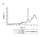
- FIG. 13 shows the absorption coefficient in the infrared region of Cz-Si and the absorption coefficient in the infrared region of FZ-Si.
- Cz-Si has a region with a low infrared transmittance near a wavelength of 9 ⁇ m.
- FZ-Si there is no region having a low infrared transmittance near the wavelength of 9 ⁇ m.
- the low-infrared transmittance region near the wavelength of 9 ⁇ m of Cz-Si is generated due to the interstitial oxygen that is taken out of the quartz crucible when the Cz-Si is produced by the Cz method. It is thought that. On the other hand, since the FZ method does not use a crucible, this problem does not occur.
- the wavelength of about 9 ⁇ m is an important region. That is, in the human sensor, it is necessary to efficiently transmit infrared rays generated by a human body having a peak at about 9.6 ⁇ m. In addition, in an infrared camera, it is necessary to efficiently transmit 8 to 12 ⁇ m infrared rays that are less absorbed by moisture in the atmosphere.
- Cz-Si is superior in manufacturing cost and design freedom as compared with FZ-Si, it is difficult to use Cz-Si as a material for an infrared transmitting member of an infrared device.
- the present invention has been made in order to improve the infrared transmittance in the vicinity of the above-mentioned Cz-Si wavelength of 9 ⁇ m and enable practical use of an infrared transmitting member made of Cz-Si.
- Patent Document 1 Japanese Patent No. 5382382
- the inventors of the present invention have found that the infrared transmittance in the vicinity of a wavelength of 9 ⁇ m of Cz—Si can be improved by satisfying the temperature, the magnitude of the pressure to be applied, and other conditions.
- the present invention makes it possible to put Cz—Si in practical use as an infrared transmitting member by using this finding.
- the present invention has been made to solve the above-described conventional problems, and as a means for processing the Cz—Si for infrared transmitting member of the present invention, Cz—Si produced by the Czochralski method is used.
- a step of preparing a step of contacting Cz-Si with a pressure jig made of a material mainly composed of a conductive material, and applying a current to the pressure jig to cause Cz-Si to self-heat, And a step of raising the temperature to a target temperature at which a desired infrared transmittance can be obtained in the vicinity of a wavelength of 9 ⁇ m and applying pressure to the pressure jig to mold Cz—Si by plastic deformation.
- the pressure jig can be composed of a pair of punches, for example.
- the current can be a pulse current, for example.
- the target temperature is preferably 650 ° C. or higher and 1050 ° C. or lower.
- the infrared transmittance in the vicinity of the wavelength of 9 ⁇ m of Cz—Si can be improved.
- target temperature is 700 degreeC or more and 1000 degrees C or less.
- the infrared transmittance in the vicinity of the wavelength of 9 ⁇ m of Cz—Si can be improved more reliably.
- the target temperature is 800 ° C. or higher and 900 ° C. or lower. In this case, the infrared transmittance in the vicinity of the wavelength of 9 ⁇ m of Cz—Si can be further improved.
- the pressure applied between the pair of pressure jigs is preferably 35.4 MPa or more and 283 MPa or less. In this case, the infrared transmittance in the vicinity of the wavelength of 9 ⁇ m of Cz—Si is improved, and the processing state is also good. More preferably, the pressure applied between the pair of pressure jigs is 141 MPa or more and 283 MPa or less. In this case, the infrared transmittance in the vicinity of the wavelength of 9 ⁇ m of Cz—Si is further improved, and the processing state is also good.
- the infrared transmitting member can be manufactured by the above-described method of processing Cz-Si for the infrared transmitting member of the present invention. In this case, it is possible to manufacture an infrared transmitting member having an improved infrared transmittance in the vicinity of a wavelength of 9 ⁇ m by using Cz—Si with low manufacturing cost and high design freedom.
- the crystal plane perpendicular to the pressure axis direction of pressure is preferably (110) plane.
- the infrared transmittance in the vicinity of the wavelength of 9 ⁇ m of Cz—Si can be improved more reliably.
- the infrared transmitting member manufactured by this infrared transmitting member manufacturing method preferably has a dislocation density of 10 2 cm ⁇ 2 or less evaluated by the etch pit method. In this case, it becomes an infrared transmitting member of excellent quality without internal defects.
- the infrared transmitting member manufactured by this infrared transmitting member manufacturing method can have a plane parallel to the pressure axis direction of the pressure as the incident surface.
- this infrared transmitting member can be used for a polarizing element.
- the infrared transmittance in the vicinity of a wavelength of 9 ⁇ m of Cz-Si can be improved.
- FIG. 1 (A-1) and (A-2) show an example of a pressure jig
- FIG. 1 (A-1) is a perspective view showing a part thereof
- FIG. 1 (1-2) is a perspective view. It is sectional drawing.
- FIG. 1B is a cross-sectional view showing another pressure jig. It is the graph which each showed the absorption coefficient of the infrared region of Cz-Si before processing, and Cz-Si after processing at processing temperature 700 degreeC, 800 degreeC, and 900 degreeC, respectively. It is the graph which showed the change of the absorption coefficient in wavelength 9 micrometers of Cz-Si at the time of changing process temperature, and the change of the absorption coefficient in 9.7 micrometers, respectively.
- FIG. 9A is a photomicrograph of Cz—Si processed at a processing temperature of 850 ° C. and a processing pressure of 141 MPa.
- FIG. 9B is a photomicrograph of Cz—Si processed at a processing temperature of 850 ° C. and a processing pressure of 283 MPa.
- FIG. 9C is a photomicrograph of Cz—Si processed at a processing temperature of 1405 ° C. and a processing pressure of 28.3 MPa by a conventional high-temperature pressing method.
- FIG. 10A is a diagram showing a crystal orientation and a dislocation line by observing a plane perpendicular to the pressing axis of Cz—Si by EBSD.
- FIG. 10A is a diagram showing a crystal orientation and a dislocation line by observing a plane perpendicular to the pressing axis of Cz—Si by EBSD.
- 10A is a diagram showing a crystal orientation and a dislocation line by observing a plane parallel to the pressing axis of Cz—Si by EBSD.
- the polarization angle of incident light is changed to 0 °, 45 °, 90 °, 135 °, and 180 °, and the angle at each angle is changed. It is the graph which showed the absorption coefficient of the infrared region.
- the plane parallel to the pressure axis direction of Cz—Si is the incident plane, and the polarization angle of incident light is 0 °, 45 °, 90 °, 135
- FIG. 12A shows the case of changing to 0 °, 45 °, and 90 °
- FIG. 12B shows the case of changing to 90 °, 135 °, and 180 °. It is the graph which showed the absorption coefficient of the infrared region of Cz-Si, and the absorption coefficient of the infrared region of FZ-Si.
- Cz—Si produced by the Czochralski method is processed to produce infrared transmitting members such as lenses (for example, convex lenses), window members, and filters.
- infrared transmitting members such as lenses (for example, convex lenses), window members, and filters.
- Cz-Si prepared by the Czochralski method is prepared.
- the prepared Cz-Si is cut into a desired shape at a desired cut angle to produce Cz-Si1 for processing.
- Cz—Si may be cut so that Alternatively, when applying pressure by bringing Cz-Si1 into contact with the punches 2 and 3, Cz-Si is cut so that the crystal plane perpendicular to the pressure axis direction of the pressure becomes the (111) plane. Also good. However, as will be described later, the cut angle of Cz—Si affects the degree of improvement in the infrared transmittance near the wavelength of 9 ⁇ m of Cz—Si.
- Cz-Si1 for processing was formed into a disk shape having a diameter of 6 mm and a thickness of 4 mm.
- Cz—Si1 for processing is formed into a desired shape.
- a pressure jig as shown in FIGS. 1A-1 and A-2 is prepared.
- the pressure jig is composed of a pair of punches 2 and 3 made of a conductive material. At least one of the punches 2 and 3 has a contact surface corresponding to a desired processed shape of Cz—Si.
- the structure of the pressing jig is arbitrary, and for example, one may be fixed and the other may be movable.
- the pair of punches 2 and 3 are accommodated in a cylindrical die 4.
- the temperature detecting element 5 is embedded in the die 4.
- a thermocouple is used for the temperature detection element 5, for example, a thermocouple is used.
- the type of the temperature detecting element 5 is arbitrary, and instead of a thermocouple, for example, a platinum resistance thermometer, thermistor, an IC temperature sensor using a temperature characteristic of a transistor, a crystal thermometer, an infrared thermopile, A thermistor, a photo-quantum photodiode, a phototransistor, or the like may be used.
- the above-described punches 2 and 3, the die 4, the temperature detecting element 5, and the pulsed current generating means described later constitute a semiconductor crystal processing apparatus used in this embodiment.
- temperature measurement is started by the temperature detection element 5 before contacting Cz-Si1 with the punches 2 and 3.
- the temperature detecting element 5 is embedded in the die 4 which is separated from Cz-Si1 by, for example, only about 1 mm, the temperature of Cz-Si1 can be measured almost accurately.
- an electric current is applied between the punch 2 and the punch 3.
- a pulse current is applied by a pulse current generator.
- the current is not limited to the pulse current, and may be a direct current or the like.
- the processing temperature of Cz-Si1 is preferably controlled to 650 ° C or higher and 1050 ° C or lower. Further, the processing temperature of Cz—Si1 is more preferably controlled to 700 ° C. or more and 1000 ° C. or less. Further, the processing temperature of Cz—Si1 is more preferably controlled to be 800 ° C. or higher and 900 ° C. or lower.
- the controlled processing temperature of Cz-Si1 affects the degree of improvement in infrared transmittance near the wavelength of 9 ⁇ m of Cz-Si.
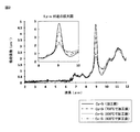
- FIG. 2 shows an absorption coefficient in the infrared region when processed at a processing temperature of 700 ° C., an absorption coefficient in the infrared region when processed at 800 ° C., and an absorption coefficient in the infrared region when processed at 900 ° C., respectively.
- FIG. 3 shows changes in the absorption coefficient of Cz—Si at a wavelength of 9 ⁇ m and changes in the absorption coefficient at 9.7 ⁇ m when the processing temperature is changed. Note that the pressure applied between the punch 2 and the punch 3 is 141 MPa.
- the large absorption coefficient in the vicinity of 9 ⁇ m derived from interstitial oxygen was improved as the processing temperature increased, and the absorption coefficient was minimized at 865 ° C.
- the absorption coefficient near 9.7 ⁇ m derived from the Si—O expansion / contraction mode increased as the processing temperature increased and reached a maximum at 865 ° C.
- interstitial oxygen moves to form clusters by heat treatment at about 800 ° C. It is considered that the absorption coefficient in the vicinity of 9 ⁇ m is improved by the movement of the interstitial oxygen.
- the reason why the absorption coefficient is improved at 865 ° C. in particular is that the diffusion of oxygen is rate-determining, and SiO 2 is precipitated from the clusters or the supersaturation degree of the clusters once generated at 865 ° C. or higher. This is thought to be due to a decrease in the amount of redox.
- the processing temperature of Cz-Si1 is controlled to 650 ° C. or higher and 1050 ° C. or lower, the absorption coefficient in the vicinity of the wavelength of 9 ⁇ m of Cz-Si1 is 3.4 cm ⁇ 1 under the conditions of this embodiment. The following can be improved. Further, if the processing temperature of Cz—Si 1 is controlled to 700 ° C. or more and 1000 ° C. or less, the absorption coefficient of Cz—Si 1 near the wavelength of 9 ⁇ m can be improved to 2.9 cm ⁇ 1 or less. Furthermore, if the processing temperature of Cz—Si1 is controlled to 800 ° C. or more and 900 ° C. or less, the absorption coefficient of Cz—Si1 near the wavelength of 9 ⁇ m can be improved to 2.3 cm ⁇ 1 or less.
- the current [A] of the pulsed current to be applied is increased until Cz-Si1 reaches the processing temperature.
- the current [A] of the pulsed current is slightly lowered and then the pulsed current is continuously applied while feedback is applied so as to maintain the processing temperature.
- the feedback is performed by feedback means (not shown) that feeds back the measured temperature of the temperature detecting element 5 to the pulsed current generator.
- the starting point is arbitrary, but pressure is applied between punch 2 and punch 3. That is, the time point at which pressure is applied may be any time point before or after the temperature of Cz-Si1 reaches the processing temperature. However, it is not preferable to apply pressure before the temperature of Cz—Si1 sufficiently rises because Cz—Si1 may break.
- the direction in which the pressure is applied is matched with the direction in which the current flows, but as shown in FIG.
- the direction in which the pressure is applied may be perpendicular to the direction in which the current flows.
- pressing direction is arbitrary, and as shown in FIGS. 1A-1, A-2, and B, pressing may be performed in a direction perpendicular to the main surface of Cz-Si1. As shown in FIG. 1C, pressure may be applied in a direction parallel to the main surface of Cz-Si1.
- the pressure applied between the punch 2 and the punch 3 can be a large value at a time. However, it is preferable to increase the size gradually or stepwise so that Cz—Si1 does not break.
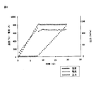
- FIG. 4 shows temporal changes in the current [A] of the pulse current, the temperature [° C.] of Cz—Si 1, and the pressure [MPa] applied between the upper punch 2 and the lower punch 3 in the present embodiment.
- the pressure (maximum pressure) applied between the punch 2 and the punch 3 affects the degree of improvement of the infrared transmittance in the vicinity of the wavelength of 9 ⁇ m of Cz-Si.
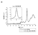
- FIG. 5 shows absorption coefficients in the infrared region of Cz-Si before processing and Cz-Si after processing at 35.4 MPa.
- the processing temperature is 850 ° C.
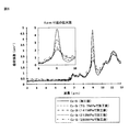
- FIG. 6 shows absorption coefficients in the infrared region of Cz—Si before processing and Cz—Si after processing at 70.7 MPa, 141 MPa, 212 MPa, and 283 MPa, respectively.
- the processing temperature is 850 ° C. for all.
- the pressure (maximum pressure) applied between the punch 2 and the punch 3 is preferably 35.4 MPa or more and 283 MPa or less. Moreover, when the degree of improvement of the absorption coefficient shown in FIG. 6 and the processed state of Cz—Si were taken into consideration, it was found that 141 MPa or more and 283 MPa or less were more preferable.
- the above-described processing temperature and processing pressure are maintained for a certain period of time.
- Cz-Si1 is taken out from punches 2, 3, and die 4, and the processing of Cz-Si for infrared transmitting members according to this embodiment is completed.
- the cooling of Cz-Si1, punches 2, 3, and die 4 may be natural cooling or accelerated cooling by a cooling means.
- the cut angle of Cz—Si is arbitrary, but in this embodiment, when applying pressure with Cz—Si 1 sandwiched between punch 2 and punch 3, the pressure is increased in the pressure axis direction.
- Cz—Si was cut so that the crystal plane perpendicular to it was the (110) plane.
- the cut angle of Cz-Si affects the degree of improvement of the infrared transmittance in the vicinity of the Cz-Si wavelength of 9 ⁇ m.
- Table 1 shows the absorption coefficient reduction rate and the change amount (mm) in the pressure axis direction of the pressure of Cz-Si1 in each case.
- the ease of annihilation of interstitial oxygen varies depending on the crystal orientation.
- the Cz-Si may be cut so that the crystal plane perpendicular to the pressure axis direction of pressure is the (110) plane. It has been found that it is advantageous for improving the infrared transmittance in the vicinity of a wavelength of 9 ⁇ m.
- FIG. 8 shows the infrared absorption coefficient of Cz-Si1 before processing, the infrared absorption coefficient of CzSi1 after processing, and the infrared absorption coefficient of FZ-Si that has not been processed for comparison.
- Cz-Si1 was cut so that the crystal plane perpendicular to the pressure axis direction of the pressure was the (110) plane.
- the processing temperature of Cz—Si was 800 ° C.
- the heating rate was 100 ° C./min
- the processing pressure was 141 MPa
- the holding time was 30 minutes.
- Cz-Si processed according to the present invention has an infrared transmittance comparable to that of FZ-Si.
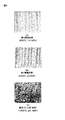
- FIG. 9A shows a photomicrograph of Cz—Si processed at a processing temperature of 850 ° C. and a processing pressure of 141 MPa.
- FIG. 9B shows a photomicrograph of Cz—Si processed at a processing temperature of 850 ° C. and a processing pressure of 283 MPa.
- FIG. 9C shows a photomicrograph of Cz—Si processed at a processing temperature of 1405 ° C. and a processing pressure of 28.3 MPa by a conventional high-temperature pressing method.
- Cz—Si according to the present embodiment shown in FIGS. 9A and 9B no defect distribution was observed, and the dislocation density was 10 2 cm ⁇ 2 or less.
- Cz-Si according to the conventional high-temperature pressing method shown in FIG. 9C dislocations are accumulated to form a subgrain structure, which deteriorates transmission characteristics.
- Cz—Si with improved infrared transmittance near a wavelength of 9 ⁇ m was fabricated by the method of the first embodiment. However, Cz-Si was cut so that the crystal plane perpendicular to the pressure axis direction of the pressure was the (110) plane.
- the processing temperature was 1100 ° C.
- the heating rate was 100 ° C./min
- the processing pressure was 141 MPa
- the holding time was 30 minutes.
- the produced Cz-Si had different dislocation lines between a plane perpendicular to the pressure axis direction and a plane parallel to the pressure axis direction. However, there was no difference in transmittance with respect to non-polarized infrared light on any surface.
- FIGS. 10A and 10B show crystal orientations and dislocation lines observed by EBSD (electron beam backscatter diffraction image). However, FIG. 10A shows a plane perpendicular to the pressing axis, and FIG. 10B shows a plane parallel to the pressing axis.
- EBSD electron beam backscatter diffraction image
- dislocation lines enter disorder in a plane perpendicular to the pressing axis direction, whereas in a plane parallel to the pressing axis direction, plastic deformation occurs. Dislocation lines are generated in a specific direction (lateral direction).
- the polarization dependence of the transmitted light according to the dislocation line formation direction was evaluated.
- the transverse polarization was set to 0 °.
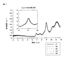
- FIG. 11 shows the measurement results when the incident light polarization angle is changed to 0 °, 45 °, 90 °, 135 °, and 180 ° with respect to the plane perpendicular to the pressure axis direction.
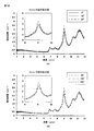
- FIG. 12 shows the measurement results when the polarization angle of the incident light is changed to 0 °, 45 °, 90 °, 135 °, and 180 ° with respect to the plane parallel to the pressure axis direction.
- FIG. 12A is divided into FIG. 12B, and FIG. 12A shows the case of changing to 0 °, 45 °, and 90 °.
- B) shows the case of changing to 90 °, 135 °, and 180 °.
- the absorption coefficient becomes the largest at a polarization angle of 90 ° in the vicinity of 9 ⁇ m.
- the absorption coefficient was the smallest.
- 0 ° is a direction perpendicular to the pressure axis direction
- 90 ° is a direction coinciding with the pressure axis direction.
- Cz-Si with improved infrared transmittance of ⁇ 9 ⁇ m by energization and pressure molding has a structure in which dislocation lines are generated in a specific direction on a plane parallel to the pressure axis direction. It was found that application to polarizing elements in the infrared region can also be expected by using this.
- the infrared transmitting member for the polarizing element of this embodiment has a plane parallel to the pressure axis direction as the incident plane.
- the infrared transmitting member for a polarizing element of the present embodiment can change the absorption coefficient by changing the angle of polarization of incident light.
Landscapes
- Physics & Mathematics (AREA)
- General Physics & Mathematics (AREA)
- Optics & Photonics (AREA)
- Crystals, And After-Treatments Of Crystals (AREA)
- Optical Filters (AREA)
- Polarising Elements (AREA)
Abstract
赤外線透過率の改善を伴った赤外線透過部材用Cz-Siの加工方法を提供する。 チョクラルスキー法により作製されたCz-Siを用意する工程と、Cz-Siを、導電性材料を主体とした材料からなる加圧冶具に当接させる工程と、加圧冶具に電流を印加することにより、Cz-Siを、自己発熱により、波長9μm付近において所望の赤外線透過率を得うる目標温度に昇温させるとともに、加圧冶具に圧力を加え、前記Cz-Siを塑性変形により成型する工程と、を備える。
Description
本発明は、赤外線透過部材用Cz-Siの加工方法に関し、さらに詳しくは、赤外線透過率の改善を伴った赤外線透過部材用Cz-Siの加工方法に関する。
また、本発明は、上記赤外線透過部材用Cz-Siの加工方法を使用した、赤外線透過部材の製造方法に関する。
さらに、本発明は、上記赤外線透過部材の製造方法により製造された赤外線透過部材に関する。
赤外線センサー、赤外線カメラなどの赤外線装置に使用するレンズ(たとえば凸レンズ)、窓部材、フィルタなどの赤外線透過部材の材料には、高い赤外線透過率が求められる。
高い赤外線透過率を備えた材料としては、たとえば、Si系半導体結晶体、Ge系半導体結晶体、ZnSeやZnSなどのワイドギャップII-VI族半導体結晶体、Ge-As-Seなどのカルコゲナイドガラス、BaF2などのフッ化物などが知られている。
これらのうち、Ge系半導体結晶体やII-VI族半導体結晶体には、高価であるという問題がある。また、カルコゲナイドガラスには、機械的強度が十分でないという問題がある。さらに、フッ化物には、耐水性が低いという問題がある。
そこで、赤外線装置など赤外線透過部材に適切な材料として、これらの問題がないSi系半導体結晶体をあげることができる。
Si系半導体結晶体の主な製造方法として、チョクラルスキー法(Cz法)とフロ-ティングゾーン法(FZ法)とが知られている。なお、以下においては、Cz法により製造されたSi系半導体結晶体をCz-Si、FZ法により製造されたSi系半導体結晶体をFZ-Siと称呼する。
Cz-Siは、一般に、FZ-Siに比べて製造コストが安い。また、FZ法は、多結晶原料棒を高周波コイルなどに通して過熱し、融解させて製造するため、FZ-Siは大口径化が難しいという問題があるが、Cz-Siにはそのような問題はない。
そこで、赤外線透過部材の材料にSi系半導体結晶体を使う場合であっても、FZ-Siを使うよりもCz-Siを使った方が、製造コストおよび設計の自由度において優れている。
しかしながら、Cz-Siには、波長9μm付近に赤外線透過率の低い領域(吸収係数の大きい領域)が存在するという問題があった。
図13に、Cz-Siの赤外域の吸収係数と、FZ-Siの赤外域の吸収係数とを示す。
図13から分かるように、Cz-Siには、波長9μm付近に赤外線透過率の低い領域が存在している。これに対し、FZ-Siには、波長9μm付近に赤外線透過率の低い領域はみられない。
Cz-Siの波長9μm付近の赤外線透過率の低い領域は、Cz法によりCz-Siを製造する際に、石英坩堝からの溶出酸素が結晶内に取り込まれ、この格子間酸素が原因で発生しているものと考えられる。一方、FZ法は坩堝を使わないので、この問題は発生しない。
赤外線装置の赤外線透過部材にとって、波長9μm付近は重要な領域である。すなわち、人感センサーにおいては、約9.6μmにピークがある人体が発生する赤外線を効率良く透過させる必要がある。また、赤外線カメラにおいては、大気中の水分による吸収が少ない8~12μmの赤外線を効率良く透過させる必要がある。
そのため、Cz-Siは、FZ-Siに比べて製造コストおよび設計の自由度において優れているにもかかわらず、赤外線装置の赤外線透過部材の材料として使用することが困難であった。
本発明は、上述したCz-Siの波長9μm付近における赤外線透過率を改善し、Cz-Siを材料にした赤外線透過部材の実用化を可能にするためになされたものである。
なお、従来、Si系半導体結晶体の加工は、研削研磨法やガスエッチング法を使用するのが一般的であった。しかしながら、近年、特許文献1(特許第5382382号公報)などに開示されるような、電流を流しながら加圧するSi系半導体結晶体の加工方法も知られている。
本発明の発明者らは、鋭意研究の結果、温度、加圧する圧力の大きさ、その他の条件を満たすことにより、Cz-Siの波長9μm付近における赤外線透過率を改善し得ることを見出した。本発明は、この知見を用いることにより、Cz-Siの赤外線透過部材としての実用化を可能にしたものである。
本発明は、上述した従来の問題を解決するためになされたものであり、その手段として本発明の赤外線透過部材用Cz-Siの加工方法は、チョクラルスキー法により作製されたCz-Siを用意する工程と、Cz-Siを、導電性材料を主体とした材料からなる加圧冶具に当接させる工程と、加圧冶具に電流を印加することにより、Cz-Siを、自己発熱により、波長9μm付近において所望の赤外線透過率を得うる目標温度に昇温させるとともに、加圧冶具に圧力を加え、Cz-Siを塑性変形により成型する工程と、を備えるようにした。
加圧治具は、たとえば1対のパンチで構成することができる。
また、電流は、たとえばパルス電流とすることができる。
目標温度は、好ましくは、650℃以上、1050℃以下である。この場合には、Cz-Siの波長9μm付近における赤外線透過率を改善することができる。より好ましくは、目標温度は700℃以上、1000℃以下である。この場合には、Cz-Siの波長9μm付近における赤外線透過率をより確実に改善することができる。さらに好ましくは、目標温度は800℃以上、900℃以下である。この場合には、Cz-Siの波長9μm付近における赤外線透過率をさらに確実に改善することができる。
1対の加圧冶具間に加えられる圧力は、好ましくは35.4MPa以上、283MPa以下である。この場合には、Cz-Siの波長9μm付近における赤外線透過率が改善され、加工状態も良好である。より好ましくは、1対の加圧冶具間に加えられる圧力は141MPa以上、283MPa以下である。この場合には、Cz-Siの波長9μm付近における赤外線透過率がより改善され、加工状態も良好である。
上述した本発明の赤外線透過部材用Cz-Siの加工方法により、赤外線透過部材を製造することができる。この場合には、製造コストが安く、設計自由ン度の高いCz-Siを使用して、波長9μm付近における赤外線透過率が改善された赤外線透過部材を製造することができる。
この赤外線透過部材の製造方法により製造された赤外線透過部材は、圧力の加圧軸方向に対して垂直な結晶面が、(110)面とされていることが好ましい。この場合には、Cz-Siの波長9μm付近における赤外線透過率をより確実に改善することができる。
また、この赤外線透過部材の製造方法により製造された赤外線透過部材は、エッチピット法により評価した転位密度が、102cm-2オーダー以下であることが好ましい。この場合には、内部欠陥のない優れた品質の赤外線透過部材になる。
また、この赤外線透過部材の製造方法により製造された赤外線透過部材は、圧力の加圧軸方向に対して平行な面を入射面とすることができる。この場合には、この赤外線透過部材を偏光素子用に使用することができる。
本発明の赤外線透過部材用Cz-Siの加工方法によれば、Cz-Siの波長9μm付近における赤外線透過率を改善することができる。
以下、図面とともに、本発明を実施するための形態について説明する。
[第1実施形態]
本実施形態においては、チョクラルスキー法により作製されたCz-Siを加工して、レンズ(たとえば凸レンズ)、窓部材、フィルタなどの赤外線透過部材を製造する。
本実施形態においては、チョクラルスキー法により作製されたCz-Siを加工して、レンズ(たとえば凸レンズ)、窓部材、フィルタなどの赤外線透過部材を製造する。
まず、チョクラルスキー法により作製されたCz-Siを用意する。
次に、用意されたCz-Siを、所望のカット角で、所望の形状にカットし、被加工用のCz-Si1を作製する。
なお、本実施形態においては、後述するように、Cz-Si1を1対のパンチ2、3に当接させて圧力を加える際に、圧力の加圧軸方向に対して垂直な結晶面が(110)面となるようにCz-Siをカットした。ただし、Cz-Siのカット角は任意であり、Cz-Si1をパンチ2、3に当接させて圧力を加える際に、圧力の加圧軸方向に対して垂直な結晶面が(100)面となるようにCz-Siをカットしても良い。あるいは、Cz-Si1をパンチ2、3に当接させて圧力を加える際に、圧力の加圧軸方向に対して垂直な結晶面が(111)面となるようにCz-Siをカットしても良い。ただし、後述するように、Cz-Siのカット角は、Cz-Siの波長9μm付近における赤外線透過率の改善度合に影響を与える。
本実施形態においては、被加工用のCz-Si1を、直径6mm、厚み4mmの円盤状とした。次に、被加工用のCz-Si1を、所望の形状に成型する。
具体的には、まず、たとえば、図1(A-1)、(A-2)に示す、加圧冶具を用意する。
加圧冶具は、導電性材料からなる1対のパンチ2、3で構成されている。パンチ2、3の少なくとも一方は、所望するCz-Siの加工形状に対応した当接面を有している。
なお、加圧治具の構造は任意であり、たとえば、一方が固定され、他方が可動となっているものであっても良い。
1対のパンチ2、3は、筒状のダイ4に収容されている。
ダイ4には、温度検知素子5が埋設されている。温度検知素子5には、たとえば、熱電対が使用される。ただし、温度検知素子5の種類は任意であり、熱電対に代えて、たとえば、白金測温抵抗体、サーミスタ、トランジスタの温度特性を利用したIC化温度センサー、水晶温度計、赤外線式のサーモパイルやサーミスタ、光量子式フォトダイオードやフォトトランジスタなどであっても良い。
以上のパンチ2、3と、ダイ4と、温度検知素子5と、後述するパルス状電流発生手段とで、本実施形態において使用する半導体結晶体の加工装置が構成されている。
次に、同じく図1(A-1)、(A-2)に示すように、カットされた被加工用のCz-Si1を、パンチ2、3に挟み込み、パンチ2、3に当接させる。
なお、前後するが、Cz-Si1をパンチ2、3に当接させる前から、温度検知素子5により温度の測定を開始する。
温度検知素子5は、Cz-Si1から、たとえば、1mm程度しか離れていないダイ4の内部に埋設されているため、ほぼ正確にCz-Si1の温度を測定することができる。
次に、パンチ2とパンチ3との間に電流を印加する。本実施形態においては、パルス状電流発生装置によりパルス電流を印加する。しかしながら、電流はパルス電流には限定されず、直流などであっても良い。
この結果、Cz-Si1に自己発熱現象が起こり、Cz-Si1の温度が急上昇する。
Cz-Si1の加工温度は、好ましくは、650℃以上、1050℃以下に制御される。また、Cz-Si1の加工温度は、より好ましくは、700℃以上、1000℃以下に制御される。また、Cz-Si1の加工温度は、さらに好ましくは、800℃以上、900℃以下に制御される。
このCz-Si1の制御される加工温度は、Cz-Siの波長9μm付近における赤外線透過率の改善度合に影響を与える。
図2に、加工温度700℃で加工した場合の赤外域における吸収係数、800℃で加工した場合の赤外域における吸収係数、900℃で加工した場合の赤外域における吸収係数をそれぞれ示す。また、図3に、加工温度を変化させた場合の、Cz-Siの波長9μmにおける吸収係数の変化、および、9.7μmにおける吸収係数の変化を示す。なお、パンチ2とパンチ3との間に加えられた圧力は、いずれも141MPaである。
図3から分かるように、格子間酸素に由来する9μm付近における大きい吸収係数は、加工温度上昇に伴い改善され、865 ℃で吸収係数は最小となった。逆に、Si-Oの伸縮モードに由来する9.7μm付近の吸収係数は、加工温度上昇に伴い大きくなり、865℃で最大となった。
一般に800℃程度での熱処理により、格子間酸素が移動してクラスタを形成することが知られている。この格子間酸素が移動することにより、9μm付近における吸収係数が改善されたものと考えられる。なお、特に865℃が吸収係数改善のピークとなる理由は、酸素の拡散が律速であることに加えて、865℃以上において、クラスタからSiO2が析出した、または、一旦生成したクラスタの過飽和度が下がり、再溶解したためと考えられる。
図3から分かるように、Cz-Si1の加工温度を650℃以上、1050℃以下に制御すれば、本実施形態の諸条件において、Cz-Si1の波長9μm付近における吸収係数を3.4cm-1以下に改善することができる。また、Cz-Si1の加工温度を700℃以上、1000℃以下に制御すれば、Cz-Si1の波長9μm付近における吸収係数を2.9cm-1以下に改善することができる。さらに、Cz-Si1の加工温度を800℃以上、900℃以下に制御すれば、Cz-Si1の波長9μm付近における吸収係数を
2.3cm-1以下に改善することができる。
2.3cm-1以下に改善することができる。
Cz-Si1が加工温度に達するまで、印加するパルス状電流の電流[A]を上昇させる。
Cz-Si1が加工温度に達した後は、パルス状電流の電流[A]をやや降下させたうえで、その後も加工温度を維持するようにフィードバックをかけながら、パルス状電流を印加し続ける。なお、フィードバックは、温度検知素子5の測定温度を、パルス状電流発生装置にフィードバックさせるフィードバック手段(図示せず)によりおこなう。
次に、開始時点は任意であるが、パンチ2とパンチ3との間に圧力を加える。すなわち、圧力をかけ始める時点は、Cz-Si1の温度が加工温度に達する前、達した時、達した後のいずれの時点のいずれであっても良い。ただし、Cz-Si1の温度が十分に上昇する前に圧力をかけると、Cz-Si1が割れる場合があるため好ましくない。
なお、本実施形態においては、図1(A-1)、(A-2)に示すように、圧力を加える方向を電流の流れる方向と一致させているが、図1(B)に示すように、圧力を加える方向を電流の流れる方向とを垂直にしても良い。
また、加圧方向も任意であり、図1(A-1)、(A-2)、(B)に示すように、Cz-Si1の主面に対して垂直方向に加圧しても良いし、図1(C)に示すように、Cz-Si1の主面に対して平行方向に加圧しても良い。
パンチ2とパンチ3との間にかける圧力は、一度に大きな値とすることもできる。しかしながら、Cz-Si1が割れることがないように、徐々に大きくしていく、あるいは段階的に大きくしていくことが好ましい。
図4に、本実施形態における、パルス状電流の電流[A]、Cz-Si1の温度[℃]、上パンチ2と下パンチ3との間にかける圧力[MPa]の時間的変化を示す。
パンチ2とパンチ3との間にかける圧力(最大圧力)は、Cz-Siの波長9μm付近における赤外線透過率の改善度合に影響を与える。
図5に、加工前のCz-Si、および35.4MPaで加工後のCz-Siの赤外域における吸収係数をそれぞれ示す。加工温度は、850℃である。
また、図6に、加工前のCz-Si、および70.7MPa、141MPa、212MPa、283MPaで加工後のCz-Siの赤外域における吸収係数をそれぞれ示す。加工温度は、いずれも850℃である。
図5から分かるように、35.4MPaでの加工で、すでに吸収係数の改善が認められる。
また、図6から分かるように、さらに圧力を大きくすると、212MPaまでは吸収係数の改善が進むが、さらに圧力を大きくした283MPaでは、逆に改善の度合いが小さくなった。ただし、283MPaで加工したCz-Siであっても、十分に良好な吸収係数であり、加工状態にも問題はなかった。
しかしながら、283MPaを超え、さらに圧力を大きくすると、吸収係数の改善の度合いが小さくなるとともに、Cz-Siにクラックが発生し始めた。
以上より、パンチ2とパンチ3との間にかける圧力(最大圧力)は、35.4MPa以上、283MPa以下が好ましいことが分かった。また、図6に示す吸収係数の改善の度合いと、Cz-Siの加工状態を考慮すると、141MPa以上、283MPa以下がより好ましいことが分かった。
図4に示すように、上述した加工温度、加工圧力を、一定時間保持する。
Cz-Si1の塑性変形量が所望の値に達したら、パルス状電流の印加を終了し、またパンチ2とパンチ3との間に圧力をかけることを終了する。なお、Cz-Si1の塑性変形量が所望の値に達したか否かは、パンチ2の変位量から確認する。
最後に、Cz-Si1、パンチ2、3、ダイ4を冷却したうえで、Cz-Si1をパンチ2、3、ダイ4から取り出し、本実施形態にかかる赤外線透過部材用Cz-Siの加工は完了する。なお、Cz-Si1、パンチ2、3、ダイ4の冷却は、自然冷却でも良いし、冷却手段により加速的に冷却しても良い。
上述のとおり、Cz-Siのカット角は任意であるが、本実施形態においては、Cz-Si1をパンチ2、パンチ3との間に挟んで圧力を加える際に、圧力の加圧軸方向に対して垂直な結晶面が(110)面となるようにCz-Siをカットした。
しかしながら、Cz-Siのカット角は、Cz-Siの波長9μm付近における赤外線透過率の改善度合に影響を与える。
図7に、Cz-Si1をパンチ2とパンチ3との間に当接させて圧力を加える際に、圧力の加圧軸方向に対して垂直な結晶面が(110)面となるようにCz-Siをカットした場合の加工後の赤外域の吸収係数、圧力の加圧軸方向に対して垂直な結晶面が(100)面となるようにCz-Siをカットした場合の加工後の赤外域の吸収係数、圧力の加圧軸方向に対して垂直な結晶面が(111)面となるようにCz-Siをカットした場合の加工後の赤外域の吸収係数をそれぞれ示す。なお、いずれも、加工温度は900℃、上パンチ2と下パンチ3との間に加えられた圧力は141MPaである。
また、表1に、各場合の、吸収係数低減率、Cz-Si1の圧力の加圧軸方向の変化量(mm)を示す。
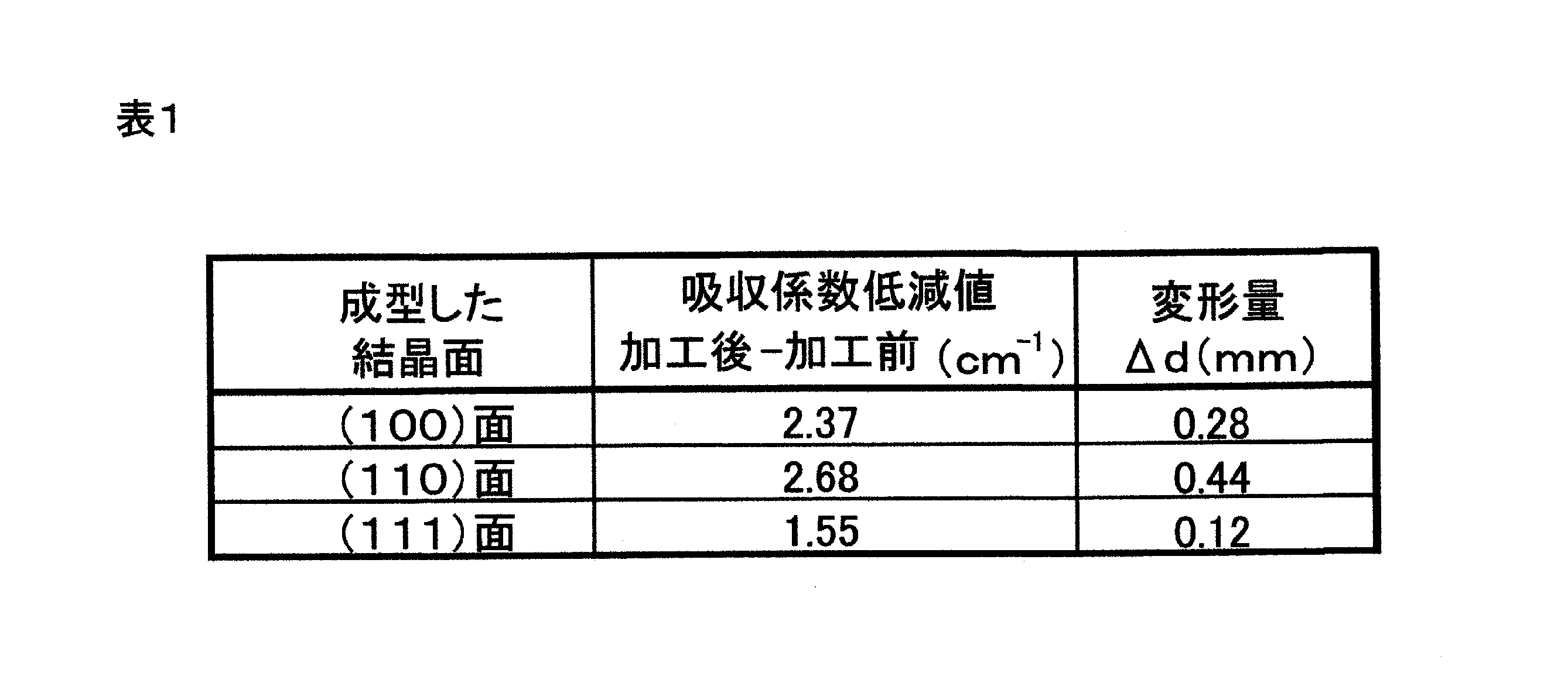
図7から分かるように、圧力の加圧軸方向に対して垂直な結晶面が(110)面である場合に、最も大きく9μm付近における透過率が改善している。また、表1から分かるように、圧力の加圧軸方向に対して垂直な結晶面が(110)面である場合に、最も変形量が大きくなっている。
以上より、格子間酸素の消滅のしやすさが、結晶の方位によって異なることが示唆されている。加工後のCz-Siを赤外線装置の赤外線透過部材に使用する場合には、圧力の加圧軸方向に対して垂直な結晶面が(110)面となるようにCz-Siをカットすることが、波長9μm付近における赤外線透過率を改善するためには有利であることが分かった。
図8に、加工前のCz-Si1の赤外域の吸収係数、加工後のCzSi1の赤外域の吸収係数、および、比較のために加工していないFZ-Siの赤外域の吸収係数をそれぞれ示す。ただし、Cz-Si1は、圧力の加圧軸方向に対して垂直な結晶面が(110)面となるようにカットした。また、Cz-Siの加工温度は800℃、昇温速度は100℃/分、加工圧力は141MPa、保持時間は30分とした。
図8から分かるように、本発明により加工されたCz-Siは、FZ-Siに対して遜色のない、赤外線透過率を備えている。
最後に、内部欠陥を確認するために、加工後のCz-Siの転位密度をエッチピット法により調べた。図9(A)に加工温度850℃、加工圧力141MPaで加工したCz-Siの顕微鏡写真を示す。図9(B)に加工温度850℃、加工圧力283MPaで加工したCz-Siの顕微鏡写真を示す。また、比較のために、図9(C)に、従来の高温プレス法で加工温度1405℃、加工圧力28.3MPaで加工したCz-Siの顕微鏡写真を示す。
図9(A)、(B)に示した、本実施形態にかかるCz-Siにおいては、欠陥分布は認められず、転位密度は102cm-2オーダー以下であった。これに対し、図9(C)に示した、従来の高温プレス法にかかるCz-Siでは、転位が集積してサブグレイン構造をとり、透過特性を劣化させていた。
以上より、本発明によれば、内部欠陥のない優れた品質のCz-Siを得ることできることが確認できた。
[第2実施形態]
第2実施形態においては、偏光素子用の赤外線透過部材を製造した。
第2実施形態においては、偏光素子用の赤外線透過部材を製造した。
まず、第1実施形態の方法により、波長9μm付近における赤外線透過率が改善されたCz-Siを作製した。ただし、Cz-Siは、圧力の加圧軸方向に対して垂直な結晶面が(110)面となるようにカットした。また、加工温度は1100℃、昇温速度は100℃/分、加工圧力は141MPa、保持時間は30分とした。
作製されたCz-Siは、加圧軸方向に対して垂直な面と平行な面とで、異なる転位線が生じた。ただし、いずれの面であっても、無偏光の赤外光に対する透過率に差異は生じなかった。
図10(A)、(B)に、EBSD(電子線後方散乱回折像)によって観察した、結晶方位および転位線を示す。ただし、図10(A)は加圧軸に対して垂直な面、図10(B)は加圧軸に対して平行な面を示している。
図10(A)、(B)から分かるように、加圧軸方向に対して垂直な面では転位線が無秩序に入るのに対し、加圧軸方向に対して平行な面では、塑性変形により、特定の方向(横方向)に転位線が生じている。
次に、転位線の形成方向による透過光の偏光依存を評価した。ここで、横偏光を0 °とした。
加圧軸方向に垂直な面に対して、入射光の偏光の角度を、0°、45°、90°、135°、180°に変化させた場合の測定結果を図11に示す。
図11から分かるように、加圧軸方向に対して垂直な面を入射面として、入射光の偏光の角度を変化させても、透過率に変化は見られなかった。これは、EBSDの結果からもわかるように、転位線が無秩序に生じており、格子間酸素も均一に存在しているためだと考えられる。
次に、加圧軸方向に平行な面に対して、入射光の偏光の角度を、0°、45°、90°、135°、180°に変化させた場合の測定結果を図12に示す。ただし、図12においては、見やすくするため、図12(A)と図12(B)に分け、図12(A)に0°、45°、90°に変化させた場合を示し、図12(B)に90°、135°、180°に変化させた場合を示している。
図12から分かるように、加圧軸方向に対して平行な面を入射面として、入射光の偏光の角度を変化させた場合、9μm付近において、偏光角が90°で最も吸収係数が大きくなり、0°、180 °の時、最も吸収係数が小さくなった。なお、0°が加圧軸方向に対して垂直な方向、90°が加圧軸方向と一致する方向である。
EBSDの測定結果と合わせて考えると、通電・加圧成型により 9μm の赤外透過率を改善したCz-Siは、加圧軸方向に対して平行な面において転位線が特定方向に生じた構造が形成しており、これを利用して、赤外領域での偏光素子への応用も期待できることが分かった。
そこで、本実施形態の偏光素子用の赤外線透過部材は、加圧軸方向に対して平行な面を入射面にした。本実施形態の偏光素子用の赤外線透過部材は、入射光の偏光の角度を変化させることにより、吸収係数を変化させることができる。
以上、本発明の第1実施形態および第2実施形態について説明した。しかしながら、本発明の内容が、上述した内容に限定されることはなく、発明の趣旨に沿って種々の変形をなすことができる。
1・・・Cz-Si
2、3・・・パンチ(パンチ2とパンチ3とで加圧治具を構成している)
4・・・ダイ
5・・・温度検知素子
2、3・・・パンチ(パンチ2とパンチ3とで加圧治具を構成している)
4・・・ダイ
5・・・温度検知素子
Claims (10)
- チョクラルスキー法により作製されたCz-Siを用意する工程と、
前記Cz-Siを、導電性材料を主体とした材料からなる加圧冶具に当接させる工程と、
前記加圧冶具に電流を印加することにより、前記Cz-Siを、自己発熱により、波長9μm付近において所望の赤外線透過率を得うる目標温度に昇温させるとともに、前記加圧冶具に圧力を加え、前記Cz-Siを塑性変形により成型する工程と、を備えた赤外線透過部材用Cz-Siの加工方法。 - 前記加圧治具が1対のパンチである、請求項1に記載された赤外線透過部材用Cz-Siの加工方法。
- 前記電流がパルス電流である、請求項1または2に記載された赤外線透過部材用Cz-Siの加工方法。
- 前記目標温度が650℃以上、1050℃以下である、請求項1ないし3のいずれか1項に記載された赤外線透過部材用Cz-Siの加工方法。
- 前記加圧冶具に加えられる圧力が35.4MPa以上、283MPa以下である、請求項1ないし4のいずれか1項に記載された赤外線透過部材用Cz-Siの加工方法。
- 前記圧力の加圧軸方向に対して垂直な前記Cz-Siの結晶面が(110)面である、請求項1ないし5のいずれか1項に記載された赤外線透過部材用Cz-Siの加工方法。
- 請求項1ないし6のいずれか1項に記載された赤外線透過部材用Cz-Siの加工方法を使用した、赤外線透過部材の製造方法。
- 請求項7に記載された赤外線透過部材の製造方法により製造された赤外線透過部材であって、前記圧力の加圧軸方向に対して垂直な結晶面が(110)面である赤外線透過部材。
- 請求項7に記載された赤外線透過部材の製造方法により製造された赤外線透過部材であって、エッチピット法により評価した転位密度が102cm-2オーダー以下である赤外線透過部材。
- 請求項7に記載された赤外線透過部材の製造方法により製造された赤外線透過部材であって、前記圧力の加圧軸方向に対して平行な面を入射面とした、偏光素子用の赤外線透過部材。
Priority Applications (1)
| Application Number | Priority Date | Filing Date | Title |
|---|---|---|---|
| JP2017511032A JP6617248B2 (ja) | 2015-04-08 | 2016-04-06 | 赤外線透過部材用Cz−Siの加工方法および赤外線透過部材の製造方法 |
Applications Claiming Priority (2)
| Application Number | Priority Date | Filing Date | Title |
|---|---|---|---|
| JP2015079583 | 2015-04-08 | ||
| JP2015-079583 | 2015-04-08 |
Publications (1)
| Publication Number | Publication Date |
|---|---|
| WO2016163419A1 true WO2016163419A1 (ja) | 2016-10-13 |
Family
ID=57073105
Family Applications (1)
| Application Number | Title | Priority Date | Filing Date |
|---|---|---|---|
| PCT/JP2016/061300 Ceased WO2016163419A1 (ja) | 2015-04-08 | 2016-04-06 | 赤外線透過部材用Cz-Siの加工方法、赤外線透過部材の製造方法および赤外線透過部材 |
Country Status (2)
| Country | Link |
|---|---|
| JP (1) | JP6617248B2 (ja) |
| WO (1) | WO2016163419A1 (ja) |
Cited By (1)
| Publication number | Priority date | Publication date | Assignee | Title |
|---|---|---|---|---|
| JP2022049597A (ja) * | 2020-09-16 | 2022-03-29 | 株式会社プラウド | 半導体結晶体の加工方法および半導体結晶体の加工装置 |
Citations (9)
| Publication number | Priority date | Publication date | Assignee | Title |
|---|---|---|---|---|
| JPH0560901A (ja) * | 1991-09-02 | 1993-03-12 | Matsushita Electric Ind Co Ltd | 赤外線光学素子およびその製造方法 |
| JP2002234774A (ja) * | 2000-12-04 | 2002-08-23 | Sumitomo Electric Ind Ltd | セラミックス光学部品及びその製造方法 |
| JP2004221464A (ja) * | 2003-01-17 | 2004-08-05 | Sony Corp | 熱電半導体の製造方法、熱電変換素子又は熱電変換装置の製造方法、並びにこれらの実施に用いる装置 |
| JP2005142370A (ja) * | 2003-11-06 | 2005-06-02 | Kazuo Nakajima | 半導体結晶体の加工方法、光・電子デバイス用ウェハー結晶体、及び太陽電池システム |
| JP2010060779A (ja) * | 2008-09-03 | 2010-03-18 | Tohoku Univ | 赤外光用の光学結晶レンズの製造方法 |
| WO2010074074A1 (ja) * | 2008-12-24 | 2010-07-01 | 株式会社 村田製作所 | 赤外光線用透過光学部材とその製造方法、光学デバイス、及び光学装置 |
| JP2013026400A (ja) * | 2011-07-20 | 2013-02-04 | Murata Mfg Co Ltd | 半導体結晶体の加工方法 |
| JP2013025037A (ja) * | 2011-07-20 | 2013-02-04 | Murata Mfg Co Ltd | 半導体結晶体の加工方法 |
| JP5382382B2 (ja) * | 2010-01-20 | 2014-01-08 | 株式会社村田製作所 | 半導体結晶体の加工方法 |
-
2016
- 2016-04-06 WO PCT/JP2016/061300 patent/WO2016163419A1/ja not_active Ceased
- 2016-04-06 JP JP2017511032A patent/JP6617248B2/ja active Active
Patent Citations (9)
| Publication number | Priority date | Publication date | Assignee | Title |
|---|---|---|---|---|
| JPH0560901A (ja) * | 1991-09-02 | 1993-03-12 | Matsushita Electric Ind Co Ltd | 赤外線光学素子およびその製造方法 |
| JP2002234774A (ja) * | 2000-12-04 | 2002-08-23 | Sumitomo Electric Ind Ltd | セラミックス光学部品及びその製造方法 |
| JP2004221464A (ja) * | 2003-01-17 | 2004-08-05 | Sony Corp | 熱電半導体の製造方法、熱電変換素子又は熱電変換装置の製造方法、並びにこれらの実施に用いる装置 |
| JP2005142370A (ja) * | 2003-11-06 | 2005-06-02 | Kazuo Nakajima | 半導体結晶体の加工方法、光・電子デバイス用ウェハー結晶体、及び太陽電池システム |
| JP2010060779A (ja) * | 2008-09-03 | 2010-03-18 | Tohoku Univ | 赤外光用の光学結晶レンズの製造方法 |
| WO2010074074A1 (ja) * | 2008-12-24 | 2010-07-01 | 株式会社 村田製作所 | 赤外光線用透過光学部材とその製造方法、光学デバイス、及び光学装置 |
| JP5382382B2 (ja) * | 2010-01-20 | 2014-01-08 | 株式会社村田製作所 | 半導体結晶体の加工方法 |
| JP2013026400A (ja) * | 2011-07-20 | 2013-02-04 | Murata Mfg Co Ltd | 半導体結晶体の加工方法 |
| JP2013025037A (ja) * | 2011-07-20 | 2013-02-04 | Murata Mfg Co Ltd | 半導体結晶体の加工方法 |
Cited By (2)
| Publication number | Priority date | Publication date | Assignee | Title |
|---|---|---|---|---|
| JP2022049597A (ja) * | 2020-09-16 | 2022-03-29 | 株式会社プラウド | 半導体結晶体の加工方法および半導体結晶体の加工装置 |
| JP7128393B2 (ja) | 2020-09-16 | 2022-08-31 | 株式会社プラウド | 半導体結晶体の加工方法および半導体結晶体の加工装置 |
Also Published As
| Publication number | Publication date |
|---|---|
| JPWO2016163419A1 (ja) | 2018-01-25 |
| JP6617248B2 (ja) | 2019-12-11 |
Similar Documents
| Publication | Publication Date | Title |
|---|---|---|
| TWI398927B (zh) | 矽晶圓及其製造方法 | |
| JP6770721B2 (ja) | シリカガラスルツボ、シリカガラスルツボの製造方法およびシリコン単結晶の引き上げ装置 | |
| KR101111436B1 (ko) | Soi 웨이퍼의 제조 방법 및 soi 웨이퍼 | |
| TWI677602B (zh) | β-GaO系單晶基板 | |
| JP2017183600A (ja) | スライス方法およびスライス装置 | |
| TW202021711A (zh) | 具有孔之玻璃基板之製造方法、及退火用玻璃積層體 | |
| JPH07144939A (ja) | ガラス多面体、使用方法ならびに製造の方法および装置 | |
| WO2002001170A1 (fr) | Procede et appareil de mesure de la temperature | |
| JP2004256388A (ja) | 六方晶系単結晶の成長方法及び同単結晶の半導体素子用基板としての利用 | |
| JP2013004825A5 (ja) | ||
| JP6617248B2 (ja) | 赤外線透過部材用Cz−Siの加工方法および赤外線透過部材の製造方法 | |
| JP6519119B2 (ja) | 偏光ガラス板の製造方法 | |
| CN114207777A (zh) | 晶体高效的sic装置晶片生产 | |
| US20110204532A1 (en) | Fabrication process for single-crystal optical devices | |
| EP1959486B1 (en) | Method of manufacturing a silicon wafer | |
| KR20110040814A (ko) | AlxGa(1-x)N 단결정의 제조 방법, AlxGa(1-x)N 단결정 및 광학 부품 | |
| CN105974510B (zh) | 一种基于石墨烯的无源消偏器及其制备方法 | |
| US20150159279A1 (en) | Process for obtaining a plurality of laminas made of a material having monocrystalline structure from an ingot | |
| TWI557775B (zh) | 用於在半導體材料中製造一層之方法及裝置 | |
| US20180201534A1 (en) | Process for joining opaque fused quartz to clear fused quartz | |
| TWI711727B (zh) | 矽晶圓 | |
| JP6591182B2 (ja) | フッ化物結晶及び光学部品 | |
| JP2008174415A (ja) | 半絶縁性GaAsウエハ及びその製造方法 | |
| Locher et al. | Large diameter sapphire dome: fabrication and characterization | |
| WO2015085014A1 (en) | System and method for obtaining laminae made of a material having known optical transparency characteristics |
Legal Events
| Date | Code | Title | Description |
|---|---|---|---|
| 121 | Ep: the epo has been informed by wipo that ep was designated in this application |
Ref document number: 16776585 Country of ref document: EP Kind code of ref document: A1 |
|
| ENP | Entry into the national phase |
Ref document number: 2017511032 Country of ref document: JP Kind code of ref document: A |
|
| NENP | Non-entry into the national phase |
Ref country code: DE |
|
| 122 | Ep: pct application non-entry in european phase |
Ref document number: 16776585 Country of ref document: EP Kind code of ref document: A1 |