WO2016159228A1 - 磁気ディスク用基板、磁気ディスク、及び、磁気ディスク用基板の製造方法 - Google Patents
磁気ディスク用基板、磁気ディスク、及び、磁気ディスク用基板の製造方法 Download PDFInfo
- Publication number
- WO2016159228A1 WO2016159228A1 PCT/JP2016/060647 JP2016060647W WO2016159228A1 WO 2016159228 A1 WO2016159228 A1 WO 2016159228A1 JP 2016060647 W JP2016060647 W JP 2016060647W WO 2016159228 A1 WO2016159228 A1 WO 2016159228A1
- Authority
- WO
- WIPO (PCT)
- Prior art keywords
- magnetic disk
- average
- disk substrate
- substrate
- polishing
- Prior art date
- Legal status (The legal status is an assumption and is not a legal conclusion. Google has not performed a legal analysis and makes no representation as to the accuracy of the status listed.)
- Ceased
Links
Images


Classifications
-
- G—PHYSICS
- G11—INFORMATION STORAGE
- G11B—INFORMATION STORAGE BASED ON RELATIVE MOVEMENT BETWEEN RECORD CARRIER AND TRANSDUCER
- G11B5/00—Recording by magnetisation or demagnetisation of a record carrier; Reproducing by magnetic means; Record carriers therefor
- G11B5/74—Record carriers characterised by the form, e.g. sheet shaped to wrap around a drum
- G11B5/82—Disk carriers
-
- G—PHYSICS
- G11—INFORMATION STORAGE
- G11B—INFORMATION STORAGE BASED ON RELATIVE MOVEMENT BETWEEN RECORD CARRIER AND TRANSDUCER
- G11B5/00—Recording by magnetisation or demagnetisation of a record carrier; Reproducing by magnetic means; Record carriers therefor
- G11B5/62—Record carriers characterised by the selection of the material
- G11B5/73—Base layers, i.e. all non-magnetic layers lying under a lowermost magnetic recording layer, e.g. including any non-magnetic layer in between a first magnetic recording layer and either an underlying substrate or a soft magnetic underlayer
-
- G—PHYSICS
- G11—INFORMATION STORAGE
- G11B—INFORMATION STORAGE BASED ON RELATIVE MOVEMENT BETWEEN RECORD CARRIER AND TRANSDUCER
- G11B5/00—Recording by magnetisation or demagnetisation of a record carrier; Reproducing by magnetic means; Record carriers therefor
- G11B5/62—Record carriers characterised by the selection of the material
- G11B5/73—Base layers, i.e. all non-magnetic layers lying under a lowermost magnetic recording layer, e.g. including any non-magnetic layer in between a first magnetic recording layer and either an underlying substrate or a soft magnetic underlayer
- G11B5/739—Magnetic recording media substrates
- G11B5/73911—Inorganic substrates
- G11B5/73913—Composites or coated substrates
-
- G—PHYSICS
- G11—INFORMATION STORAGE
- G11B—INFORMATION STORAGE BASED ON RELATIVE MOVEMENT BETWEEN RECORD CARRIER AND TRANSDUCER
- G11B5/00—Recording by magnetisation or demagnetisation of a record carrier; Reproducing by magnetic means; Record carriers therefor
- G11B5/62—Record carriers characterised by the selection of the material
- G11B5/73—Base layers, i.e. all non-magnetic layers lying under a lowermost magnetic recording layer, e.g. including any non-magnetic layer in between a first magnetic recording layer and either an underlying substrate or a soft magnetic underlayer
- G11B5/739—Magnetic recording media substrates
- G11B5/73911—Inorganic substrates
- G11B5/73917—Metallic substrates, i.e. elemental metal or metal alloy substrates
- G11B5/73919—Aluminium or titanium elemental or alloy substrates
-
- G—PHYSICS
- G11—INFORMATION STORAGE
- G11B—INFORMATION STORAGE BASED ON RELATIVE MOVEMENT BETWEEN RECORD CARRIER AND TRANSDUCER
- G11B5/00—Recording by magnetisation or demagnetisation of a record carrier; Reproducing by magnetic means; Record carriers therefor
- G11B5/62—Record carriers characterised by the selection of the material
- G11B5/73—Base layers, i.e. all non-magnetic layers lying under a lowermost magnetic recording layer, e.g. including any non-magnetic layer in between a first magnetic recording layer and either an underlying substrate or a soft magnetic underlayer
- G11B5/739—Magnetic recording media substrates
- G11B5/73911—Inorganic substrates
- G11B5/73921—Glass or ceramic substrates
-
- G—PHYSICS
- G11—INFORMATION STORAGE
- G11B—INFORMATION STORAGE BASED ON RELATIVE MOVEMENT BETWEEN RECORD CARRIER AND TRANSDUCER
- G11B5/00—Recording by magnetisation or demagnetisation of a record carrier; Reproducing by magnetic means; Record carriers therefor
- G11B5/84—Processes or apparatus specially adapted for manufacturing record carriers
-
- G—PHYSICS
- G11—INFORMATION STORAGE
- G11B—INFORMATION STORAGE BASED ON RELATIVE MOVEMENT BETWEEN RECORD CARRIER AND TRANSDUCER
- G11B5/00—Recording by magnetisation or demagnetisation of a record carrier; Reproducing by magnetic means; Record carriers therefor
- G11B5/84—Processes or apparatus specially adapted for manufacturing record carriers
- G11B5/8404—Processes or apparatus specially adapted for manufacturing record carriers manufacturing base layers
-
- B—PERFORMING OPERATIONS; TRANSPORTING
- B82—NANOTECHNOLOGY
- B82Y—SPECIFIC USES OR APPLICATIONS OF NANOSTRUCTURES; MEASUREMENT OR ANALYSIS OF NANOSTRUCTURES; MANUFACTURE OR TREATMENT OF NANOSTRUCTURES
- B82Y10/00—Nanotechnology for information processing, storage or transmission, e.g. quantum computing or single electron logic
-
- B—PERFORMING OPERATIONS; TRANSPORTING
- B82—NANOTECHNOLOGY
- B82Y—SPECIFIC USES OR APPLICATIONS OF NANOSTRUCTURES; MEASUREMENT OR ANALYSIS OF NANOSTRUCTURES; MANUFACTURE OR TREATMENT OF NANOSTRUCTURES
- B82Y40/00—Manufacture or treatment of nanostructures
Definitions
- the present invention relates to a magnetic disk substrate having a pair of main surfaces, a magnetic disk, and a method for manufacturing the magnetic disk substrate.
- an aluminum alloy substrate or a glass substrate has been suitably used for a magnetic disk used as one of information recording media.
- the density of magnetic recording has been increased.
- the magnetic recording information area is miniaturized by extremely shortening the flying distance from the magnetic recording surface of the magnetic head.
- magnetic recording is performed by forming perpendicular magnetization in the magnetic layer of the magnetic disk.
- in order to achieve a low flying height of a magnetic head that is essential for a high recording density hard disk drive device there is an increasing demand for reducing the surface roughness of the magnetic disk substrate.
- a substrate for a magnetic recording medium which is made of a non-magnetic material and has a surface roughness curve with a surface roughness Ra of 30 nm or less with an inclination angle of a surface cross-sectional curve of 2.0 degrees or less or a period of 83 nm or less.
- a substrate for a perpendicular magnetic recording medium having a surface shape with a surface roughness Ra of 0.15 nm or less within a range of Ra is known (Patent Document 1). According to the substrate, the crystal orientation of the magnetic particles formed on the substrate can be improved to reduce the noise of the recording layer (or magnetic layer) of the magnetic recording medium.
- the surface roughness Ra is obtained from the result of measurement with an atomic force microscope.
- the atomic force microscope measures the surface roughness using, for example, a member made of single crystal Si at the probe tip.
- the magnetic disk characteristics may not always be improved.
- BER Code Error Rate: Bit Error Rate
- This BER did not have a sufficient correlation with the surface roughness Ra, and some had a large BER even if the surface roughness Ra was small.
- the present invention provides an index of the surface roughness of the magnetic disk substrate that correlates well with the above-described magnetic disk characteristics, and the magnetic disk substrate, magnetic disk, and magnetic disk substrate having excellent magnetic disk characteristics.
- An object is to provide a manufacturing method.
- One embodiment of the present invention is a magnetic disk substrate.
- the magnetic disk substrate has a pair of main surfaces,
- the arithmetic mean roughness Ra of the main surface is 0.11 nm or less.
- the surface roughness Ra is a value measured using an atomic force microscope including a probe having a carbon nanofiber rod-like member provided at the probe tip.
- the magnetic disk substrate is Having a pair of main surfaces; Of the surface irregularities on the main surface, the average area of the regions occupied by each of the plurality of convex portions having a height of 0.1 [nm] or more from the average surface of the surface irregularities is 25 [nm 2 / piece] or less. It is.
- the surface unevenness of the main surface is a value measured using an atomic force microscope provided with a probe having a carbon nanofiber rod-like member provided at the probe tip.
- the average of the area occupied by each of the plurality of convex portions having a height of 0.1 [nm] or more from the average surface of the surface unevenness is 20 [nm 2 / piece] or less.
- the average of the area occupied by each of the plurality of convex portions having a height of 0.1 [nm] or more from the average surface of the surface unevenness and the height of 0.2 [nm] or more from the average surface of the surface unevenness is preferable that the difference between the average of the area occupied by each of the plurality of convex portions having a thickness is 13 [nm 2 / piece] or less.
- the carbon nanofiber rod-shaped member provided at the probe tip has a Young's modulus of 100 GPa or less. It is preferable that the rod-shaped member has conductivity and one end of the rod-shaped member is connected to the ground.
- the surface roughness Ra or the surface unevenness is obtained by changing the position of the probe according to the surface unevenness of the main surface of the probe so that the probe vibrates with a constant amplitude. It is preferable to obtain from position information. In the measurement with the atomic force microscope, it is preferable that the probe is vibrated at a frequency of 30 to 400 [KHz] with a spring constant of 0.1 to 80 [N / m].
- the substrate is preferably a substrate for a magnetic disk for energy-assisted magnetic recording.
- Another embodiment of the present invention is a magnetic disk in which at least a magnetic film is formed on the surface of the magnetic disk substrate.
- Yet another embodiment of the present invention is a method for manufacturing a magnetic disk substrate.
- the manufacturing method After the grinding treatment, in the polishing treatment step, the surface irregularities of the main surface measured using an atomic force microscope provided with a probe having a carbon nanofiber rod-like member provided at the probe tip is 0. 0 from the average surface of the surface irregularities.
- the pair of main surfaces of the substrate is provided with a machining allowance of 30 ⁇ m or less so that the average of the area occupied by each of the plurality of convex portions having a height of 1 [nm] or more is 25 [nm 2 / piece] or less. Grind.
- the polishing process step First polishing the pair of main surfaces of the magnetic disk substrate using an acidic polishing liquid, After the first polishing, the main surface of the glass substrate is subjected to a second polishing using an alkaline polishing liquid, The second polishing preferably includes shortening the polishing time as compared with the first polishing.
- the average of the area occupied by each of the plurality of convex portions having a height of 0.1 [nm] or more from the average surface of the surface irregularities is 20 [nm 2 / piece] or less. It is preferable that
- the average area of the regions occupied by each of the plurality of convex portions having a height of 0.2 [nm] or more from the average surface of the surface irregularities is 12 [nm 2 / piece] or less. It is preferable that
- another aspect of the present invention is a method for manufacturing a magnetic disk substrate, which includes a step of determining surface irregularities on the main surface of the magnetic disk substrate and determining suitability as a magnetic disk substrate.
- the determination process includes Measure the surface irregularities of the main surface of the magnetic disk substrate using an atomic force microscope equipped with a probe with a carbon nanofiber rod-like member provided at the probe tip, From the surface unevenness data obtained by measurement, the area of each of the plurality of protrusions having a height of 0.1 [nm] or more from the average surface of the surface unevenness among the surface unevenness of the main surface When the average is 25 [nm 2 / piece] or less, it is determined that the measured substrate is adopted as the magnetic disk substrate.
- the determination is that the average area of the regions occupied by each of the plurality of convex portions having a height of 0.1 [nm] or more from the average surface roughness of the main surface is 20 [nm 2 / piece] or less. It is preferable to use for.
- the determination is that the average area of the regions occupied by each of the plurality of convex portions having a height of 0.2 [nm] or more from the average surface roughness of the main surface is 12 [nm 2 / piece] or less. It is preferable to include.
- a magnetic disk substrate having excellent magnetic disk characteristics can be provided.
- the present inventor considered the reason why BER does not sufficiently correlate with surface roughness Ra as follows. That is, the probe tip of the atomic force microscope used for measuring the surface roughness Ra is usually a pyramid shape or a cone shape made of Si (silicon) single crystal. When the tip of the probe comes into contact with the surface of the magnetic disk substrate to be measured, a new unevenness is created in the surface unevenness that should be measured, and this new unevenness is measured as the surface unevenness of the main surface of the magnetic disk substrate. The present inventor thought. For this reason, the surface unevenness information of the main surface including the new unevenness formed by the probe tip is not the surface unevenness to be originally measured. In addition, the surface of the probe tip may be oxidized to form a non-conductive SiO 2 layer on the surface.
- a silicon single crystal is very hard and has the same level as a glass substrate.
- the influence of newly formed irregularities was not visible, but the main surface of the glass substrate became ultra-smooth and the recording density was 1 for 2.5 inch size. It is inferred that it has been affected by the unevenness that is newly created by dramatically increasing to more than 750 GB per sheet, 3.5 inches size and more than 1000 GB per sheet. Therefore, the magnetic disk substrate of the present invention is particularly preferably used for a magnetic disk having a recording density of 750 gigabytes or more per nominal 2.5 inch size magnetic disk.
- the magnetic disk when the magnetic disk is nominally 3.5 inches in size, it is preferably used for a magnetic disk having a recording density equivalent to 1000 gigabytes or more per disk.
- the magnetic disk substrate of the present invention can also be applied to a magnetic disk having a recording density equivalent to 500 gigabytes or more per nominal 2.5 inch size.
- the probe tip when an excessive force is applied to the probe tip, the probe tip is deformed to reduce the formation of new irregularities on the main surface of the magnetic disk substrate. It preferably has the property of returning to the shape. Those that remain bent when they are greatly deformed and are difficult to return to the original are not preferred as probe tips.
- the inventor of the present application measures the surface unevenness of the main surface of the magnetic disk substrate by using a probe having a rod-shaped member made of carbon nanofiber at the probe tip or a rod-shaped member having a Young's modulus of 100 GPa or less at the probe tip, The present inventors have found that the correlation between the measurement results and the magnetic disk characteristics is high, and have come to the following embodiments.
- (Definition) -Surface roughness Ra as used in this specification is arithmetic mean roughness Ra based on JISB0601: 2013. Measurement of surface irregularities on the main surface of the magnetic disk substrate is performed using an atomic force microscope with a measurement point of 512 points ⁇ 128 points in a rectangular evaluation region of 1 ⁇ m ⁇ 0.25 ⁇ m. Therefore, the surface roughness Ra is a value of surface irregularities in a region of 1 ⁇ m ⁇ 0.25 ⁇ m.
- the magnetic disk In the magnetic disk, the central portion of the disk shape is cut out concentrically to form an annular plate shape, and rotates around the center of the ring during magnetic recording.
- the magnetic disk includes a substrate and at least a magnetic layer.
- an adhesion layer, a soft magnetic layer, a nonmagnetic underlayer, a perpendicular magnetic recording layer, a protective layer, a lubricating layer, and the like are formed.
- the substrate a glass substrate or a substrate made of an aluminum alloy on which a plating layer is formed is used.
- the adhesion layer for example, a Cr alloy or the like is used.
- the adhesion layer functions as an adhesive layer with the glass substrate, it is not necessary for a substrate in which a NiP plating layer is formed on an aluminum alloy base material.
- a soft magnetic layer for example, a CoTaZr alloy or the like is used.
- a nonmagnetic underlayer for example, a granular nonmagnetic layer is used.
- a granular magnetic layer is used for the perpendicular magnetic recording layer.
- a material made of hydrogen carbon is used for the protective layer.
- a fluorine-based resin or the like is used.
- a CrTi alloy adhesion layer, a CoTaZr alloy soft magnetic layer, a NiW alloy seed layer, a Ru underlayer, CoCrPt—SiO 2 are formed on both main surfaces of a glass substrate.
- a TiO 2 alloy first magnetic recording layer, a CoCrPtB alloy second magnetic recording layer, and a hydrogenated carbon protective layer are sequentially formed. Further, a perfluoropolyether lubricating layer is formed on the uppermost layer of the formed layer by dipping.
- an FePt-based or CoPt-based alloy can be used as the magnetic recording layer.
- Aluminosilicate glass, soda lime glass, borosilicate glass, or the like can be used as a material for a glass substrate for a magnetic disk used as an example of this embodiment.
- aluminosilicate glass can be suitably used in that it can be chemically strengthened and a glass substrate for a magnetic disk excellent in the smoothness of the main surface and the strength of the substrate can be produced. From the above viewpoint, it is more preferable to use amorphous aluminosilicate glass.
- the glass which has the following glass composition can also be used.
- the glass transition point of glass having the following glass composition is preferably 600 ° C. or higher, and more preferably 650 ° C. or higher. Glass having a glass transition point of 600 ° C. or higher can be suitably used for a magnetic disk substrate for energy-assisted magnetic recording that uses both magnetism and heat when performing magnetic recording.
- the glass substrate of the present embodiment has a SiO 2 content of 57 to 75% and an Al 2 O 3 content of 5 to 20%, for example, in terms of mass%. (However, the total amount of SiO 2 and Al 2 O 3 is 74% or more.
- Glass composition 2 Further, the glass substrate of the present embodiment is converted to oxide standards and expressed in mol%, SiO 2 is 50 to 75%, Al 2 O 3 is more than 0% and 15% or less, Li 2 O, Na 2 O and 5 to 35% in total of at least one component selected from K 2 O, 0 to 20% in total of at least one component selected from MgO, CaO, SrO, BaO and ZnO, and ZrO 2 , Amorphous aluminosilicate having a composition having a total of 0 to 10% of at least one component selected from TiO 2 , La 2 O 3 , Y 2 O 3 , Ta 2 O 5 , Nb 2 O 5 and HfO 2 Glass may also be used.
- a glass transition point (Tg) may be 600 degreeC or more, for example.
- a base material made of an aluminum alloy is used as the magnetic disk substrate, a substrate in which a NiP plating layer for increasing the surface hardness is formed on the surface of the base material is used.
- FIG. 1 is a diagram showing the external shape of a magnetic disk substrate before the above-described magnetic layer and the like of this embodiment are formed.
- the magnetic disk substrate a glass substrate or a substrate in which a NiP plating layer is formed on an aluminum alloy base material is preferably used. These substrates can be used as magnetic disk substrates for perpendicular magnetic recording or energy-assisted magnetic recording.
- the magnetic disk substrate 1 in this embodiment is a donut-shaped thin plate substrate in which an inner hole 2 is formed. The size of the substrate does not matter.
- the magnetic disk substrate 1 can be used for a nominal 1.8 to 3.5 inch size substrate, for example.
- the plate thickness is not particularly limited, and can be, for example, 0.3 to 3 mm.
- the magnetic disk substrate of the present embodiment (hereinafter also simply referred to as a substrate) includes a pair of main surfaces provided on both sides, a side wall surface of the substrate extending perpendicularly to the pair of main surfaces, a side wall surface, and a main surface. And a chamfered surface extending from the side wall surface with an inclination to the side wall surface and connected to the main surface. Sidewall surfaces and chamfered surfaces are not shown. The side wall surface and the chamfered surface are formed at the outer peripheral side and inner peripheral end portions of the substrate. Note that part or all of the chamfered surface may be formed in an arc shape in a cross-sectional view.
- the surface roughness Ra of the main surface is 0.11 nm or less.
- the surface roughness Ra is a value measured using an atomic force microscope having a probe in which a rod-shaped member of carbon nanofiber is provided at the probe tip.
- FIG. 2 is a diagram for explaining a part of the probe including the probe tip used by the atomic force microscope.
- a carbon nanofiber rod-like member 4 is provided at the tip of the probe 3 shown in FIG.
- carbon nanofibers are members filled with carbon atoms.
- a carbon nanotube is a hollow one having a six-membered ring network made of carbon as an outer wall and a hollow inside, and its vertical cross section in the longitudinal direction is an annual ring (concentric).
- a rod-like carbon nanofiber is used at the probe tip.
- the probe 3 is formed by etching a single crystal of Si to form a cantilever whose end is pointed in a pyramid shape as shown in FIG.
- the rod-shaped member 4 of the carbon nanofiber is formed on the pointed portion of the pyramid shape.
- the diameter (diameter) of the rod-shaped member 4 of the carbon nanofiber is, for example, 3 to 60 [nm], and the length is, for example, 5 to 1000 [nm].
- the carbon nanofiber rod-like member 4 preferably has an appropriate Young's modulus and is easily elastically deformed.
- the Young's modulus is preferably 100 GPa or less, for example.
- the Young's modulus is more preferably 50 GPa or less, and further preferably 30 GPa or less.
- the lower limit of Young's modulus is not particularly limited, but the lower limit is, for example, 1 GPa.
- the radius of curvature of the tip of the rod-shaped member 4 is preferably 1 to 30 [nm] from the viewpoint that the surface roughness Ra with high accuracy can be calculated.
- the surface roughness parameters including the surface roughness Ra of the substrate using an atomic force microscope using a probe having such a probe tip. Specifically, when measuring while moving the probe on the main surface of the substrate, the probe according to the surface irregularities of the main surface of the substrate so that the probe that vibrates at a constant frequency vibrates with a constant amplitude. Information on the position of the probe obtained by changing the position is obtained as measurement data. In the present embodiment, it is preferable to obtain the surface unevenness parameter including the surface roughness Ra of the main surface of the substrate from the measurement data. This measurement is called Intermittent contact mode.
- the main surface of the substrate to be evaluated is scanned while hitting it with a probe that vibrates up and down at high speed, so that it is easy to detect fine irregularities on the hard surface, and it is said that accurate measurement is possible.
- the surface roughness Ra obtained by this measurement as a parameter of the surface unevenness, and the average of the area of each of the plurality of convex portions having a height of 0.1 [nm] or more from the average surface of the surface unevenness, It can be used as an index of surface irregularities of a glass substrate for magnetic disk, which correlates well with magnetic disk characteristics.
- the magnetic disk substrate correlates well with the magnetic disk characteristics when the probe is vibrated at a vibration constant of 0.1 to 80 [N / m] and a vibration frequency of 30 to 400 [kHz]. It is preferable in that an index of surface irregularities can be obtained.
- the spring constant is more preferably 0.5 to 4 [N / m].
- the frequency is more preferably 50 to 100 [kHz].
- the area of each of the plurality of convex portions having a height of 0.1 [nm] or more from the average surface of the surface irregularities Is 25 [nm 2 / piece] or less, preferably 20 [nm 2 / piece] or less from the viewpoint of exhibiting excellent magnetic disk characteristics.
- the average surface is a surface set so that the volume of the convex portion protruding from the average surface is equal to the volume of the concave portion recessed from the average surface.
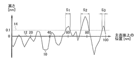
- FIG. 3 is a two-dimensional representation of an example of contour curve elements of surface irregularities on the main surface of the glass substrate. The horizontal axis in FIG.
- FIG. 3 represents the position on the main surface in a certain direction along the main surface of the glass substrate, and the vertical axis represents the height of the surface irregularities.
- two-dimensional surface irregularities are used instead of the three-dimensional surface irregularities formed on the main surface.
- a straight line at a position in the height direction of 0.1 [nm] or more from the average line 12 of the contour curve element 10 is represented by a level line 14.
- the average line 12 is a straight line indicating a level in the height direction in which the areas of the convex portions protruding from the average line 12 and the concave portions are the same.
- corrugation occupies is applied to the three-dimensional surface unevenness
- an area having a height of 0.1 nm or more from the average surface is extracted from the image data of the surface unevenness measured using an atomic force microscope, and the height of 0.1 nm or more is extracted by image analysis software.
- the average of the area occupied by one protrusion is calculated by calculating the number of protrusions and the area of the area occupied by the protrusions and dividing the area by the number. In this case, the number of protrusions and the area occupied by the protrusions are calculated by excluding the one-pixel extracted area and the straight line area (with a circularity of 0) in image analysis.
- the area of the horizontal cross section of the convex portion at a height of 0.1 nm from the average surface is obtained as the area of each of the plurality of convex portions having a height of 0.1 nm or more from the average surface of the surface irregularities. be able to.
- an area having a height of 0.2 nm or more from the average surface is extracted from the image data of the surface unevenness, and the number of protrusions having a height of 0.2 nm or more and the area occupied by the protrusions are extracted by image analysis software. By calculating the area and dividing the area by the number, the average area of the area occupied by one convex portion is calculated.
- the area of the horizontal cross section of the convex portion at a height of 0.2 nm from the average plane is obtained as the area of each of the plurality of convex portions having a height of 0.2 nm or more from the average plane of the surface irregularities.
- the average of the area occupied by each of the plurality of convex portions having a height of 0.2 [nm] or more from the average surface roughness of the main surface of the glass substrate is excellent in magnetic disk characteristics. From the standpoint of exhibiting, it is preferably 13 [nm 2 / piece] or less, and more preferably 10 [nm 2 / piece] or less.
- the average of the area of each of the plurality of convex portions having a height of 0.1 [nm] or more from the average surface roughness of the main surface of the substrate is calculated. Setting it to 25 [nm 2 / piece] or less, preferably 20 [nm 2 / piece] or less means that the average area of the area occupied by one convex portion is the same as that of the main surface of the conventional magnetic disk substrate. It corresponds to making it smaller than the convex part. As a result, the variation in crystal orientation of the magnetic layer that generates perpendicular magnetization formed on the main surface of the substrate as a magnetic disk can be reduced.
- the average area of the areas occupied by the plurality of convex portions having a height of 0.2 [nm] or more from the average surface roughness of the main surface of the substrate is 13 [nm 2 / piece] or less.
- variation in crystal orientation of the magnetic layer that generates perpendicular magnetization formed on the main surface of the substrate can be further reduced.
- the surface roughness Ra of the main surface measured using an atomic force microscope having a probe in which a rod-shaped member of carbon nanofiber is provided at the probe tip is 0.11 nm or less.
- the conventional probe tip is a polygonal cone or cone and does not use carbon nanofiber rods. Therefore, the probe tip creates new irregularities on the main surface of the substrate during measurement, and information on the surface irregularities originally intended to be measured is new. It is easy to be buried by unevenness. For this reason, it is difficult to measure actual surface irregularities. For this reason, even if the substrate has a surface roughness Ra of 0.11 nm or less according to the conventional surface roughness measurement, some substrates have low BER and others have high BER.
- the rod-like member is elastically deformed and bent even when an excessive force is applied, so that the probe tip is newly added to the main surface of the substrate during measurement. It is possible to accurately measure actual surface irregularities without creating irregularities.
- the average of the area occupied by each of the plurality of convex portions having a height of 0.1 [nm] or more from the average surface roughness of the main surface of the substrate is 25 [nm 2 / piece] or less, preferably There is no conventional substrate having a thickness of 20 [nm 2 / piece] or less, and in the conventional magnetic disk substrate, the average area of the area occupied by each of the convex portions is larger than 25 [nm 2 / piece].
- Carbon nanotubes with a six-membered ring network made of carbon as the outer wall and hollow inside (hollow) and whose vertical cross section in the longitudinal direction are annual rings (concentric) are regular and highly crystalline. Since it has a strong structure, it has a high Young's modulus.
- a solid rod-like carbon nanofiber having a low Young's modulus and being easily elastically deformed rather than a structure having a high Young's modulus like that of a carbon nanotube.
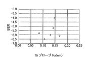
- FIG. 4 shows the correlation between the surface roughness Ra (Si probe Ra) measured by an atomic force microscope using a Si probe having a conventional probe tip made of Si and the bit error rate (hereinafter abbreviated as BER). It is a figure which shows that is low.
- the vertical axis of FIG. 4, BER is expressed by x when represented by 10 x. For example, when the BER is 10 ⁇ 5.0 , the vertical axis in FIG. 4 represents ⁇ 5.0.
- the correlation between the surface roughness Ra and the BER which is one of the magnetic disk characteristics, is low.
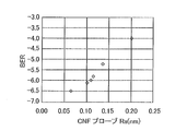
- a carbon nanofiber (CNF) rod-shaped member is used as the probe tip, as shown in FIG.
- FIG. 5 is a diagram showing a high correlation between BER and surface roughness Ra (CNF probe Ra) measured by an atomic force microscope using a probe whose tip is composed of a CNF rod-shaped member. .
- the vertical axis of FIG. 5 is also represented by x when BER is represented by 10 x .
- a BER of 10 ⁇ 5.0 is represented as ⁇ 5.0.
- this embodiment provides an index of the surface roughness of the main surface of the glass substrate for magnetic disk that has a high correlation with BER, which is the magnetic disk characteristic, and provides a glass substrate for magnetic disk with a low BER. it can.
- a Si member when used at the probe tip as in the prior art, a SiO 2 oxide film having low electrical conductivity is formed on the tip surface, and static electricity tends to accumulate at the probe tip. During measurement of the surface roughness Ra, accumulated static electricity tends to adversely affect the operation of the probe.
- it is preferable that one end of the rod-like member is connected to ground. In this case, even if static electricity that adversely affects the probe operation due to friction between the main surface of the glass substrate and the tip of the probe occurs, the static electricity can be quickly released through the ground, so that measurement is hardly affected. For this reason, accurate surface roughness Ra can be measured.
- Such a glass substrate for magnetic disks can be realized by a method for manufacturing a glass substrate for magnetic disks described below.
- the average area of the regions occupied by each of the plurality of convex portions having a height of 0.1 [nm] or more from the average surface of the surface unevenness, and the average surface of the surface unevenness The difference between the average area of the regions occupied by each of the plurality of convex portions having a height of 0.2 [nm] or more from the average is 13 [nm 2 / piece] or less, and the BER is favorably maintained. This is preferable.
- the reason for this is not necessarily clear, but by setting the difference to 13 [nm 2 / piece] or less, the shape of the protrusions on the surface of the substrate can be easily aligned, and variations in the magnetic particle size can be suppressed when a magnetic disk is used. I guess it is possible. If there are many variations in the shape of the convex portions on the surface of the substrate, the number of magnetic particles that grow abnormally increases, and as a result, it is presumed that noise during recording and reproduction increases and BER deteriorates.
- the surface roughness of the main surface of the magnetic disk substrate is a value measured using an atomic force microscope including a probe in which a carbon nanofiber rod-like member is provided at the probe tip.
- the occupation area of the plurality of convex portions having a height of 0.1 [nm] or more from the average surface roughness of the magnetic disk substrate is 20 with respect to the area of the measurement range (1 ⁇ m ⁇ 0.25 ⁇ m). % Or less, more preferably 18% or less. Furthermore, the number of convex portions having a height of 0.1 [nm] or more from the average surface of the surface irregularities of the magnetic disk substrate is preferably 500 or more in the measurement range of 1 ⁇ m ⁇ 0.25 ⁇ m. A range of 600 or more and 800 or less is more preferable.
- the number of projections having a height of 0.2 [nm] or more from the average surface of the surface irregularities is preferably 500 or less, and 150 or more and 450 or less in the measurement range of 1 ⁇ m ⁇ 0.25 ⁇ m. A range is more preferable.
- the surface roughness Ra described above is preferably 0.11 nm or less, but may be larger than 0.11 nm, and the upper limit of the surface roughness Ra is 0.00. It is preferably 15 nm.
- each of the plurality of convex portions having a height of 0.1 [nm] or more from the average surface of the surface unevenness occupies.
- the average area is preferably 25 [nm 2 / piece] or less, but may be larger than 25 [nm 2 / piece], and the upper limit of the average is 30 [nm 2 / piece]. preferable.
- a glass blank as a material for a plate-like magnetic disk glass substrate having a pair of main surfaces is prepared.
- a glass blank is produced by press molding.
- the glass blank is produced by press molding.
- a circular inner hole is formed in the central portion of the produced glass blank to form a ring-shaped (annular) glass substrate (circular hole forming process).
- shape processing is performed on the glass substrate in which the inner hole is formed (shape processing processing). Thereby, a glass substrate is obtained.
- end face polishing is performed on the glass substrate (end face polishing treatment). Grinding with a fixed abrasive is performed on the main surface of the glass substrate subjected to end face polishing (grinding treatment).
- grinding treatment is performed on the main surface of the glass substrate subjected to end face polishing (grinding treatment).
- the main surface of the glass substrate is polished (polishing process). In the polishing process, polishing is performed a plurality of times. During this multiple polishing, chemical strengthening may be performed on the glass substrate as necessary (chemical strengthening treatment). Thereafter, ultrasonic cleaning is performed on the glass substrate after the polishing treatment.
- the glass substrate for magnetic disks is obtained through the above processing. Hereinafter, each process will be described in detail.
- Circular hole forming treatment A disk-shaped glass substrate having circular holes is obtained by forming circular inner holes using a drill or the like on a glass blank.
- (C) Shape processing In the shape processing, chamfering is performed on the end surface of the glass substrate after the circular hole formation processing.
- the chamfering process is performed using a grinding wheel or the like.
- a side wall surface of the substrate that extends perpendicularly to the main surface of the glass substrate on the end surface of the glass substrate, and a chamfer surface that is provided between the side wall surface and the main surface and extends at an angle to the side wall surface. are formed.
- (D) End face polishing process In the end face polishing process, mirror finishing is performed on the inner peripheral side end face and the outer peripheral side end face of the glass substrate by an end face polishing process using a polishing liquid containing abrasive grains.
- the main surface of the glass substrate is ground by using a double-side grinding apparatus having a planetary gear mechanism. Specifically, the main surfaces on both sides of the glass substrate are ground while holding the outer peripheral side end face of the glass substrate in the holding hole provided in the holding member of the double-side grinding apparatus.
- the double-sided grinding apparatus has a pair of upper and lower surface plates (upper surface plate and lower surface plate), and a glass substrate is sandwiched between the upper surface plate and the lower surface plate. Then, by moving either one or both of the upper surface plate and the lower surface plate and relatively moving the glass substrate and each surface plate, both main surfaces of the glass substrate can be ground.
- polishing treatment Next, the ground surface of the ground glass substrate is polished. Specifically, the main surface on both sides of the glass substrate is polished while holding the outer peripheral side end face of the glass substrate in a holding hole provided in the polishing carrier of the double-side polishing apparatus. Polishing is performed using a double-side polishing apparatus.
- a glass substrate In the double-side polishing apparatus, a glass substrate is sandwiched between a pair of upper and lower surface plates.
- An annular flat polishing pad (for example, a resin polisher) is attached to the upper surface of the lower surface plate and the bottom surface of the upper surface plate as a whole. Then, by moving either the upper surface plate or the lower surface plate, or both, the main surface of the glass substrate is polished by relatively moving the glass substrate and each surface plate.
- the polishing is performed three times from the first to the third polishing from the viewpoint that the surface roughness Ra of the main surface of the glass substrate of this embodiment is 0.11 nm or less, or from the average surface of the surface irregularities. This is preferable because the average area of the regions occupied by the plurality of convex portions having a height of [nm] or more is 25 [nm 2 / piece] or less.
- the purpose of the first polishing is to remove scratches and distortions remaining on the main surface after grinding, or to adjust minute surface irregularities (microwaveness, roughness) and to make a mirror surface.
- abrasive grains such as cerium oxide or zirconia are used and supplied between the polishing pad of the double-side polishing apparatus and the main surface of the glass substrate, and the main surface of the glass substrate is polished.
- the abrasive grains used for the first polishing are, for example, cerium oxide particles having an average particle diameter d50 of 0.1 to 1.5 ⁇ m.
- the purpose of the second polishing is mirror polishing for further smoothing the main surface of the glass substrate.
- a polishing liquid containing colloidal silica having an average particle diameter d50 of 5 to 20 nm as free abrasive grains is supplied between the polishing pad of the double-side polishing apparatus and the main surface of the glass substrate. Polished.
- the liquid property of the polishing liquid is preferably acidic from the viewpoint of the polishing rate and the reduction of foreign particles on the surface after polishing, more preferably pH 1 to 4.
- the machining allowance is preferably 1 to 5 ⁇ m in terms of plate thickness (the total amount of machining allowances on both main surfaces).
- the degree of smoothness of the main surface of the glass substrate is further improved.
- a polishing liquid containing colloidal silica having an average particle diameter d50 of 30 to 100 nm as free abrasive grains is supplied between the polishing pad of the double-side polishing apparatus and the main surface of the glass substrate. Is polished.
- the liquidity of the polishing liquid is preferably alkaline from the viewpoint of smoothness, and more preferably pH 11-13.
- the machining allowance is preferably 0.05 to 1 ⁇ m in terms of plate thickness.
- an acidic polishing liquid is preferably used
- an alkaline polishing liquid is preferably used in the third polishing.
- An alkaline polishing liquid has a lower polishing rate than an acidic polishing liquid, and polishing with an alkaline polishing liquid can be performed after polishing with an acidic liquid from the viewpoint that high-accuracy polishing can be realized. preferable.
- the average particle diameter of d50 of colloidal silica is more preferably twice or more that of the second polishing, and further more preferably 3 times or more. By doing so, it becomes possible to remove fine and sharp streaks formed on the substrate surface by the small-diameter silica abrasive grains with the relatively large-diameter silica abrasive grains.
- the surface of the magnetic disk substrate can be formed.
- the machining allowance is less than that in the second polishing.
- the polishing time of the third polishing is, for example, 1/3 or less of the polishing time of the second polishing, and further 1 ⁇ 4 or less, so that the surface roughness Ra can be 0.11 nm or less.
- the average area of the regions occupied by each of the plurality of convex portions having a height of 0.1 [nm] or more from the average surface of the surface irregularities is 25 [nm 2 / piece] or less.
- the allowance for removing the glass substrate in the first to third polishing is 30 ⁇ m or less, preferably 25 ⁇ m or less, and more preferably 20 ⁇ m or less.
- the present invention is achieved by combining the liquidity of the polishing liquid, the particle size of the colloidal silica, and the machining allowance so as to be in the above ranges, respectively.
- a glass substrate for a magnetic disk suitable for the above can be obtained.
- the surface roughness Ra of the main surface when measured using an atomic force microscope having a probe having a carbon nanofiber rod-like member provided at the probe tip can be made 0.11 nm or less.
- the average surface roughness of the magnetic disk substrate can be reduced.
- the average area of the regions occupied by each of the plurality of convex portions having a height of 0.1 [nm] or more can be 25 [nm 2 / piece] or less. That is, the pair of main surfaces of the substrate is polished with a machining allowance of 30 ⁇ m or less so that the average is 25 [nm 2 / piece] or less.
- (G) Chemical strengthening treatment When chemically strengthening a glass substrate, for example, a mixed melt of potassium nitrate and sodium sulfate is used as the chemical strengthening solution, and the glass substrate is immersed in the chemical strengthening solution.
- the chemical strengthening process is performed, for example, between the first polishing and the second polishing.
- the chemical strengthening process is not essential and may not be performed. In this way, a magnetic disk glass substrate is produced.
- NiP plating layer formation the surface of the grind substrate (base material) is subjected to NiP plating to obtain an aluminum alloy substrate.
- An aluminum alloy is lightweight and excellent in workability, but the surface hardness cannot sufficiently satisfy the requirements of a magnetic disk, so that a NiP plating layer is formed on the surface of the grind substrate in order to prevent damage to the substrate.
- the thickness of the NiP plating layer is, for example, several tens of ⁇ m. Further, annealing is performed to relieve internal stress of the NiP plating layer.
- polishing Grinding is performed on the grind substrate after the plating layer is formed in order to remove waviness and fine waviness and smooth the surface.
- the NiP plating layer is polished in a plurality of stages by using a polishing slurry in which a polishing pad (for example, a resin polisher) and free abrasive grains including alumina abrasive grains are dispersed.
- the substrate thus polished is washed to obtain a magnetic disk substrate.
- the surface roughness Ra of the main surface can be reduced to 0.11 nm or less by performing a plurality of steps of polishing in the same manner as the polishing of the glass substrate manufacturing method described above.
- a pair of substrates is set so that the average area of the regions occupied by the plurality of convex portions having a height of 0.1 [nm] or more from the average surface unevenness is 25 [nm 2 / piece] or less. Can be polished with a machining allowance of 30 ⁇ m or less.
- the average area of the regions occupied by the plurality of convex portions having a height of 0.1 [nm] or more from the average surface of the surface irregularities described above is 25 [nm 2 / piece] or less.
- the present invention can be applied to a process for determining whether or not a substrate is within a range in which magnetic disk characteristics are allowed as a magnetic disk substrate in a method for manufacturing a magnetic disk substrate.
- the surface roughness of the main surface of the substrate is measured using an atomic force microscope having a probe having a carbon nanofiber rod-shaped member, for example, a rod-shaped member having a Young's modulus of 100 GPa or less at the probe tip.
- the average area of the area occupied by each of the plurality of convex portions having a height of 0.2 [nm] or more from the average surface roughness of the main surface is 12 [nm 2 / piece] or less. It is also preferable to include it in the determination.
- Such a method is implemented by an atomic force microscope and an arithmetic unit that obtains the average from the surface roughness data obtained by the atomic force microscope.
- the determination condition may include that the surface roughness Ra that can be obtained from the surface roughness data obtained by the above-described measurement is 0.11 [nm] or less.
- the above screening method can be applied to a glass substrate for magnetic disk and an aluminum alloy substrate for magnetic disk. The magnetic disk characteristics of a magnetic disk manufactured using such a magnetic disk substrate can be improved.
- the BER can be 10 ⁇ 5.8 or less.
- Example 1 In order to confirm the effect of this embodiment, using the glass substrate manufacturing method described above for a plurality of types of glass substrates, the conditions for the second polishing and the third polishing were changed to obtain six types of 18 glass substrates. Produced. Three pieces were produced for each type.
- the glass of the glass substrate had the glass composition described above.
- the surface roughness of the glass substrate was measured with an atomic force microscope using one of each of the six types of glass substrates using a probe using a carbon nanofiber rod-shaped member having a diameter of 20 nm and a length of 200 nm at the probe tip. The measurement was performed under the following conditions.
- Measurement area Rectangular area of 1 ⁇ m ⁇ 0.25 ⁇ m ⁇ Number of measurement points: 512 points ⁇ 128 points (512 points for 1 ⁇ m, 128 points for 0.25 ⁇ m) ⁇ Measurement mode: Intermittent contact mode ⁇ Frequency: 70KHz ⁇ Spring constant of probe: 4N / m
- the surface roughness of the glass substrate was measured with an atomic force microscope on one of each of the six types of glass substrates using a pyramidal probe whose probe tip was made of Si. The measurement was performed under the conditions described above.
- a magnetic disk substrate is manufactured by providing a magnetic layer and the like on the remaining one of the various types of glass substrates as described above, and an HDD (hard disk) together with a magnetic head equipped with a DFH (disk flying height) mechanism.
- the DFH element part is gradually protruded, and the protrusion amount when the tip contacts the substrate surface is used as a reference, with the protrusion amount reduced by 1 nm, that is, the back-off amount becomes 1 nm.
- the BER value of the produced magnetic disk was obtained.
- the linear recording density at the time of signal recording was 93 kbit / mm. Table 1 below shows the evaluation results of six types of glass substrates.
- the six types of glass substrates in Table 1 are represented as Samples 1 to 6.
- the column “Surface roughness Ra (CNF probe Ra)” shows the results of measurement using carbon nanofibers at the probe tip, and the column “Surface roughness Ra (Si probe Ra)” shows a pyramid shape at the probe tip.
- the results of measurement using Si of FIG. The numerical value x in the “BER” column in Table 1 represents 10 x .
- the surface roughness Ra (CNF probe Ra) has a higher correlation with the BER than the surface roughness Ra (Si probe Ra). Recognize. Further, from Table 1, by setting the surface roughness Ra (CNF probe Ra) to 0.11 nm or less, the BER, which is the allowable range of the magnetic disk characteristics, is 10 ⁇ 5.8 or less, preferably 10 ⁇ 6. It can be seen that it can be reduced to 0.0 or less. At this time, the average of the area occupied by each of the plurality of convex portions having a height of 0.1 [nm] or more from the average surface roughness of the glass substrates of Samples 1 to 6 is 30 [nm 2]. / Piece].
- Example 2 Further, in order to confirm the effect of the present embodiment, four types of glass substrates are manufactured by changing the conditions of the second polishing and the third polishing using the glass substrate manufacturing method described above for a plurality of types of glass substrates. A substrate was produced. The glass of the glass substrate had the glass composition described above. For each of the four types of glass substrates, the surface roughness of the glass substrate was measured with an atomic force microscope using a probe using a carbon nanofiber rod-shaped member having a diameter of 20 nm and a length of 200 nm at the probe tip. The measurement conditions were the same as in Experimental Example 1.
- a magnetic disk substrate is manufactured by providing a magnetic layer on one of the various types of glass substrates manufactured, and incorporated in an HDD (Hard Disk Drive Device) together with a magnetic head equipped with a DFH (Disk Flying Height) mechanism.
- the BER value of the magnetic disk was obtained under the same conditions as above.
- Table 2 below shows the evaluation results of four types of glass substrates.
- the column of “0.1 nm or more” indicates the average area of the regions occupied by each of the plurality of convex portions having a height of 0.1 [nm] or more from the average surface of the surface unevenness.
- the column “.2 nm or more” indicates the average of the area of each of the plurality of convex portions having a height of 0.2 [nm] or more from the average surface of the surface irregularities.
- the numerical value x in the “BER” column in Table 2 represents 10 x .
- the surface roughness Ra of the glass substrates of Samples 7 to 10 were all 0.15 nm or less. From Table 2, samples 7 and 8 in which the average of the area occupied by each of the plurality of convex portions having a height of 0.1 [nm] or more from the average surface of the surface irregularities is 25 [nm 2 / piece] or less are as follows. BER becomes 10 ⁇ 5.8 or less, and it can be seen that the magnetic disk characteristics are improved.
- the magnetic disk glass substrate, the magnetic disk substrate manufacturing method, and the magnetic disk substrate determination method of the present invention have been described in detail.
- the present invention is not limited to the above-described embodiment and the like, and the gist of the present invention. It goes without saying that various improvements and changes may be made without departing from the scope of the invention.
Landscapes
- Engineering & Computer Science (AREA)
- Chemical & Material Sciences (AREA)
- Inorganic Chemistry (AREA)
- Metallurgy (AREA)
- Manufacturing & Machinery (AREA)
- Nanotechnology (AREA)
- Ceramic Engineering (AREA)
- Crystallography & Structural Chemistry (AREA)
- Physics & Mathematics (AREA)
- Theoretical Computer Science (AREA)
- Mathematical Physics (AREA)
- Condensed Matter Physics & Semiconductors (AREA)
- General Physics & Mathematics (AREA)
- Magnetic Record Carriers (AREA)
- Manufacturing Of Magnetic Record Carriers (AREA)
- Recording Or Reproducing By Magnetic Means (AREA)
Abstract
Description
当該磁気ディスク用基板は、一対の主表面を有し、
前記主表面の算術平均粗さRaは、0.11nm以下である。
前記表面粗さRaは、カーボンナノファイバの棒状部材をプローブ先端に設けたプローブを備える原子間力顕微鏡を用いて測定した値である。
当該磁気ディスク用基板は、
一対の主表面を有し、
前記主表面の表面凹凸のうち、該表面凹凸の平均面から0.1[nm]以上の高さを有する複数の凸部のそれぞれが占める領域の面積の平均は25[nm2/個]以下である。
前記主表面の表面凹凸は、カーボンナノファイバの棒状部材をプローブ先端に設けたプローブを備える原子間力顕微鏡を用いて測定した値である。
前記棒状部材は導電性を有し、前記棒状部材の一方の端がアースに接続されている、ことが好ましい。
前記表面粗さRaあるいは前記表面凹凸は、前記プローブが一定の振幅で振動するように、前記プローブの前記主表面の表面凹凸に応じて前記プローブの位置を変化させることにより得られる、前記プローブの位置の情報から求める、ことが好ましい。
前記原子力顕微鏡の測定では、前記プローブを、0.1~80[N/m]のばね定数で、振動数30~400[KHz]で振動させる、ことが好ましい。
研削処理後、研磨処理工程において、カーボンナノファイバの棒状部材をプローブ先端に設けたプローブを備える原子間力顕微鏡を用いて測定した前記主表面の表面凹凸について、前記表面凹凸の平均面から0.1[nm]以上の高さを有する複数の凸部のそれぞれが占める領域の面積の平均が25[nm2/個]以下となるように前記基板の一対の主表面を30μm以下の取り代で研磨する。
磁気ディスク用基板の一対の主表面を酸性の研磨液を用いて第1の研磨をし、
前記第1の研磨後、ガラス基板の主表面をアルカリ性の研磨液を用いて第2の研磨をし、
前記第2の研磨では、前記第1の研磨に比べて研磨時間を短くする、ことを含む、ことが好ましい。
カーボンナノファイバの棒状部材をプローブ先端に設けたプローブを備える原子間力顕微鏡を用いて磁気ディスク用基板の主表面の表面凹凸を測定し、
測定して得られる表面凹凸のデータから、前記主表面の表面凹凸のうち、該表面凹凸の平均面から0.1[nm]以上の高さを有する複数の凸部のそれぞれが占める領域の面積の平均を求め、前記平均が25[nm2/個]以下である場合、測定した基板を磁気ディスク用基板として採用する判定を行なう。
また、このプローブ先端の表面は酸化されて、非導電性のSiO2層が表面に形成される場合がある。この場合、プローブ先端を一定の振動数で振動させて、磁気ディスク用基板の主表面と近接あるいは接触させて、磁気ディスク用基板の主表面の表面凹凸を測定するとき、磁気ディスク用基板としてガラス基板が用いられるときは特にプローブ先端に静電気が生じ易く、ガラス基板にも静電気が生じ易い。この結果、プローブ先端の挙動は静電気の影響を受けて、ガラス基板の表面凹凸を精度良く測定することができない場合がある。このような問題は、ガラス基板の表面凹凸の程度を従来に比べていっそう小さくすることにより生じた問題であり、従来のガラス基板の表面凹凸の範囲内では生じない問題である。特に、シリコン単結晶は非常に硬く、ガラス基板と同程度であるため、上記のような現象がおきやすい。従来のガラス基板の表面粗さと記録密度のレベルでは、新たに作られる凹凸の影響が見えなかったが、ガラス基板の主表面が超平滑になったことと記録密度が2.5インチサイズで1枚あたり750ギガバイト以上、3.5インチサイズで1枚あたり1000ギガバイト以上と飛躍的に上がったことで新たに作られる凹凸の影響を受けるようになったと推察される。したがって、本件発明の磁気ディスク用基板は、公称2.5インチサイズの磁気ディスク1枚あたり750ギガバイト相当以上の記録密度の磁気ディスクに用いられることが特に好ましい。また、磁気ディスクが公称3.5インチサイズの場合は、1枚あたり1000ギガバイト相当以上の記録密度の磁気ディスクに用いることが好ましい。なお、公称2.5インチサイズ1枚あたり500ギガバイト相当以上の記録密度の磁気ディスクに対して本件発明の磁気ディスク用基板を適用することも可能である。
また、プローブ先端に過大な力が加わったとき、プローブ先端が変形することで磁気ディスク用基板の主表面における新たな凹凸の形成が緩和されるが、プローブ先端は、この変形が大きい場合にもとの形状に戻る性質を有することが好ましい。大きく変形したとき、曲がったままになり、元に戻りにくいものはプローブ先端として好ましくない。
本願発明者は、プローブ先端にカーボンナノファイバからなる棒状部材あるいはヤング率が100GPa以下の棒状部材をプローブ先端に設けたプローブを用いて磁気ディスク用基板の主表面の表面凹凸を測定することにより、測定結果と磁気ディスク特性との間の相関が高いことを見出し、下記実施形態を想到するに至った。
・本明細書でいう表面粗さRaは、JIS B0601:2013に準拠した算術平均粗さRaである。
・磁気ディスク用基板の主表面の表面凹凸の測定は、原子間力顕微鏡を用いて、1μm×0.25μmの矩形の評価領域にて測定点数を512ポイント×128ポイントとして行なわれる。
したがって、表面粗さRaは、1μm×0.25μmの領域における表面凹凸の値である。
・本明細書でいう、表面凹凸の平均面からx[nm](xは、0.1や0.2等の正数)以上の高さを有する複数の凸部のそれぞれが占める領域の面積とは、換言すれば、磁気ディスク用基板の表面凹凸の平均面からx[nm]の高さで、磁気ディスク用基板を切断した時の磁気ディスク用基板の切断された凸部それぞれの断面積をいう。また、さらに換言すれば、磁気ディスク用基板の表面凹凸の測定データから算出される平均面を基準面として、そこからx[nm]の高さの平面によって得られる当該表面凹凸の断面を仮定したとき、当該断面において得られる1以上の領域のそれぞれの面積、のことをいう。
磁気ディスクは、円板形状の中心部分が同心円形状にくり抜かれて円環板状を成し、磁気記録の際、この円環の中心の周りに回転する。磁気ディスクは、基板と、少なくとも磁性層と、を備える。なお、磁性層以外には、例えば、付着層、軟磁性層、非磁性下地層、垂直磁気記録層、保護層および潤滑層等が形成される。基板には、ガラス基板又はめっき層を形成したアルミニウム合金からなる基板が用いられる。付着層には、例えばCr合金等が用いられる。付着層は、ガラス基板との接着層として機能するため、アルミニウム合金基材にNiPめっき層を形成した基板の場合には不要である。軟磁性層には、例えばCoTaZr合金等が用いられる。非磁性下地層には、例えばグラニュラー非磁性層等が用いられる。垂直磁気記録層には、例えばグラニュラー磁性層等が用いられる。保護層には、水素カーボンからなる材料が用いられる。潤滑層には、例えばフッ素系樹脂等が用いられる。
また、エネルギーアシスト磁気記録方式用の磁気ディスクとする場合、磁気記録層としてFePt系やCoPt系の合金を用いることもできる。
本実施形態のガラス基板は、例えば質量%表示にて、SiO2を57~75%、Al2O3を5~20%、(ただし、SiO2とAl2O3の合計量が74%以上)、ZrO2、HfO2、Nb2O5、Ta2O5、La2O3、Y2O3およびTiO2を合計で0%超6%以下、Li2Oを1%超9%以下、Na2Oを5~18%(ただし、質量比Li2O/Na2Oが0.5以下)、K2Oを0~6%、MgOを0~4%、CaOを0%超5%以下(ただし、MgOとCaOの合計量は5%以下であり、かつCaOの含有量はMgOの含有量よりも多い)、SrO+BaOを0~3%、有する組成からなるアモルファスのアルミノシリケートガラスを用いることができる。
また、本実施形態のガラス基板は、酸化物基準に換算し、モル%表示で、SiO2を50~75%、Al2O3を0%超15%以下、Li2O、Na2O及びK2Oから選択される少なくとも1種の成分を合計で5~35%、MgO、CaO、SrO、BaO及びZnOから選択される少なくとも1種の成分を合計で0~20%、ならびにZrO2、TiO2、La2O3、Y2O3、Ta2O5、Nb2O5及びHfO2から選択される少なくとも1種の成分を合計で0~10%、有する組成からなるアモルファスのアルミノシリケートガラスであってもよい。なお、この組成のガラス基板をエネルギーアシスト磁気記録方式用の磁気ディスク向けに用いるガラス基板とする場合、例えばガラス転移点(Tg)が600℃以上となるようにガラス組成を適宜調整すればよい。
磁気ディスク用基板として、アルミニウム合金製の基材を用いる場合、この基材の表面に、表面硬度を高めるためのNiPめっき層が形成されたものが用いられる。
図1は、本実施形態の上述した磁性層等が形成される前の磁気ディスク用基板の外観形状を示す図である。本実施形態において、磁気ディスク用基板としては、ガラス基板又はアルミニウム合金製の基材にNiPめっき層を形成した基板が好適に用いられる。これら基板は、垂直磁気記録方式又はエネルギーアシスト磁気記録方式の磁気ディスク用基板として用いることができる。
図1に示すように、本実施形態における磁気ディスク用基板1は、内孔2が形成された、ドーナツ型の薄板の基板である。基板のサイズは問わない。磁気ディスク用基板1は、例えば公称1.8~3.5インチサイズの基板に使用することができる。板厚についても特に制限はなく、例えば0.3~3mmとすることができる。
本実施形態の磁気ディスク用基板(以降、単に基板ともいう)は、両側に設けられた一対の主表面と、一対の主表面に対して垂直に延びる基板の側壁面と、側壁面と主表面の間に設けられ、側壁面から側壁面に対して傾斜して延び、主表面に接続する面取り面とを有する。側壁面及び面取り面は図示されていない。側壁面及び面取り面は、基板の外周側及び内周側の端部に形成されている。なお、面取り面の一部又は全部は、断面視において円弧状に形成されていてもよい。
カーボンナノファイバの棒状部材4の、径(直径)は例えば3~60[nm]であり、長さは例えば5~1000[nm]である。
カーボンナノファイバの棒状部材4は適度なヤング率を有して弾性変形し易いことが好ましく、基板両側の主表面の凹凸を精度良く検知する観点からヤング率は例えば100GPa以下であることが好ましい。この場合、ヤング率が50GPa以下であることがより好ましく、30GPa以下であるとさらに好ましい。この場合、ヤング率の下限は特に制限されないが、下限は、例えば1GPaである。
なお、棒状部材4の先端曲率半径は1~30[nm]であることが、精度の高い表面粗さRaを算出することができる点から好ましい。
図3は、ガラス基板の主表面の表面凹凸の輪郭曲線要素の一例を2次元で表した図である。図3の横軸は、ガラス基板の主表面に沿ったある方向の主表面上の位置を表し、縦軸は、表面凹凸の高さを表している。以下の説明では、主表面上に形成される3次元の表面凹凸の代わりに、2次元の表面凹凸を用いて説明する。図3では、輪郭曲線要素10の平均線12から0.1[nm]以上の高さ方向の位置の直線がレベル線14で表されている。平均線12とは、平均線12から突出した凸部と凹んだ凹部の面積が同じである高さ方向のレベルを示す直線である。このとき、レベル線14から突出する凸部は3つあり、凸部の占める領域の長さは、S1、S2、S3である。したがって、このときの複数のそれぞれが占める1個あたりの凸部の占める領域の線分の平均は、(S1+S2+S3)/3となる。したがって、本実施形態では、このような2次元の表面凹凸の各凸部が占める領域の線分を、ガラス基板の主表面上に形成される3次元の表面凹凸に適用する。
より具体的には、原子間力顕微鏡を用いて測定した表面凹凸の画像データから、平均面から0.1nm以上の高さを持つエリアを抜き出し、画像解析ソフトにより、0.1nm以上の高さの凸部の個数と凸部の占める領域の面積を算出して、上記面積を個数で割り算することにより1つの凸部が占める領域の面積の平均を算出する。この場合、画像解析上、抜き出したエリアが1ピクセルのものと、直線のもの(サーキュラリティが0のもの)については除外して、凸部の個数と凸部の占める領域の面積を算出する。これにより、表面凹凸の平均面から0.1nm以上の高さを有する複数の凸部のそれぞれが占める領域の面積として、平均面から0.1nmの高さにおける凸部の水平断面の面積を求めることができる。同様に、表面凹凸の画像データから、平均面から0.2nm以上の高さを持つエリアを抜き出し、画像解析ソフトにより、0.2nm以上の高さの凸部の個数と凸部の占める領域の面積を算出して、上記面積を個数で割り算することにより1つの凸部が占める領域の面積の平均を算出する。これにより、表面凹凸の平均面から0.2nm以上の高さを有する複数の凸部のそれぞれが占める領域の面積として、平均面から0.2nmの高さにおける凸部の水平断面の面積を求めることができる。
本実施形態では、ガラス基板の主表面の表面凹凸の平均面から0.2[nm]以上の高さを有する複数の凸部のそれぞれが占める領域の面積の平均は、優れた磁気ディスク特性を発揮する点から13[nm2/個]以下であることが好ましく、10[nm2/個]以下であることがより好ましい。
特に、基板の主表面の表面凹凸の平均面から0.1[nm]以上の高さを有する複数の凸部のそれぞれが占める領域の面積の平均は25[nm2/個]以下、好ましくは20[nm2/個]以下である基板は従来存在せず、従来の磁気ディスク用基板では、上記凸部のそれぞれが占める領域の面積の平均は25[nm2/個]より大きい。
なお、炭素によって作られる六員環ネットワークを外壁とし内部が空洞であり(中空であり)、その長手方向垂直断面は年輪状(同心円状)であるカーボンナノチューブについては、規則的で結晶性の高強度の構造を有するためヤング率が高く、そのために撓みにくく、過大な力が加わった場合に曲がったまま元に戻ることができない場合がある。このため、カーボンナノチューブのような高ヤング率の構造ではなく、ヤング率が低く弾性変形し易い中実の棒状のカーボンナノファイバを用いることが好ましい。ヤング率が100GPa以下の棒状部材をプローブ先端に用いることで、測定中プローブ先端がガラス基板の主表面に新たな凹凸を作ることはなく、実際の表面凹凸を正確に測定することができる。
これに対して、本実施形態では、プローブ先端としてカーボンナノファイバ(CNF)の棒状部材を用いるので、図5に示すように、表面粗さRa(CNFプローブRa)と磁気ディスク特性の1つであるBERとの間の相関は高い。図5は、プローブ先端がCNFの棒状部材で構成されたプローブを用いた原子間力顕微鏡で測定される表面粗さRa(CNFプローブRa)と、BERとの相関が高いことを示す図である。図5の縦軸も、図4と同様に、BERは10xで表されるときのxで表している。BERが例えば10-5.0は、-5.0と表している。図4及び図5に示す例で用いた基板の主表面の表面凹凸のうち、表面凹凸の平均面から0.1[nm]以上の高さを有する複数の凸部のそれぞれが占める領域の面積の平均は略一定であった。
このように、本実施形態は、磁気ディスク特性であるBERと相関の高い磁気ディスク用ガラス基板の主表面の表面粗さの指標を提供し、BERの低い磁気ディスク用ガラス基板を提供することができる。
このような磁気ディスク用ガラス基板は、以下に説明する磁気ディスク用ガラス基板の製造方法により実現することができる。
また、上述したように、表面粗さRaが0.11nm以下である磁気ディスク用基板では、表面凹凸の平均面から0.1[nm]以上の高さを有する複数の凸部のそれぞれが占める領域の面積の平均は25[nm2/個]以下であることが好ましいが、25[nm2/個]より大きくてもよく、その平均の上限は30[nm2/個]であることが好ましい。
次に、本実施形態の磁気ディスク用ガラス基板の製造方法を説明する。先ず、一対の主表面を有する板状の磁気ディスク用ガラス基板の素材となるガラスブランクを作製する。例えば、プレス成形処理によるガラスブランクを作製する。なお、本実施形態ではガラスブランクをプレス成形で作製するが、周知のフロート法、リドロー法、あるいはフュージョン法でガラス板を形成し、ガラス板から上記ガラスブランクと同じ形状のガラスブランクを切り出してもよい。次に、作製されたガラスブランクの中心部分に円形状の内孔を形成しリング形状(円環状)のガラス基板とする(円孔形成処理)。次に、内孔を形成したガラス基板に対して形状加工を行う(形状加工処理)。これによりガラス基板が得られる。次に、ガラス基板に対して端面研磨を行う(端面研磨処理)。端面研磨の行われたガラス基板の主表面に、固定砥粒による研削を行う(研削処理)。次に、ガラス基板の主表面に研磨を行う(研磨処理)。研磨処理では、複数回の研磨を行う。この複数回の研磨の間に、必要に応じてガラス基板に対して化学強化を行ってもよい(化学強化処理)。その後、研磨処理後のガラス基板に対して超音波洗浄を行う。以上の処理を経て、磁気ディスク用ガラス基板が得られる。以下、各処理について、詳細に説明する。
熔融ガラス流を切断機により切断し、切断された熔融ガラス塊を一対の金型のプレス成形面の間に挟みこみ、プレスしてガラスブランクを成形する。所定時間プレスを行った後、金型を開いてガラスブランクが取り出される。
ガラスブランクに対してドリル等を用いて円形状の内孔を形成することにより円形状の孔があいたディスク状のガラス基板を得る。
形状加工処理では、円孔形成処理後のガラス基板の端面に対する面取り加工を行う。面取り加工は、研削砥石等を用いて行なわれる。面取り加工により、ガラス基板の端面に、ガラス基板の主表面に対して垂直に延びる基板の側壁面と、この側壁面と主表面の間に設けられ、側壁面に対して傾斜して延びる面取り面とを有する端面が形成される。
端面研磨処理では、ガラス基板の内周側端面及び外周側端面に対して、研磨砥粒を含んだ研磨液を用いた端面研磨処理により鏡面仕上げを行う。
研削処理では、遊星歯車機構を備えた両面研削装置を用いて、ガラス基板の主表面に対して研削を行う。具体的には、ガラス基板の外周側端面を、両面研削装置の保持部材に設けられた保持孔内に保持しながらガラス基板の両側の主表面の研削を行う。両面研削装置は、上下一対の定盤(上定盤および下定盤)を有しており、上定盤および下定盤の間にガラス基板が狭持される。そして、上定盤または下定盤のいずれか一方、または、双方を移動させ、ガラス基板と各定盤とを相対的に移動させることにより、ガラス基板の両主表面を研削することができる。
次に、研削したガラス基板の主表面に研磨が施される。具体的には、ガラス基板の外周側端面を、両面研磨装置の研磨用キャリアに設けられた保持孔内に保持しながらガラス基板の両側の主表面の研磨が行われる。研磨は、両面研磨装置を用いて行なわれる。両面研磨装置は、上下一対の定盤の間にガラス基板が狭持される。下定盤の上面及び上定盤の底面には、全体として円環形状の平板の研磨パッド(例えば、樹脂ポリッシャ)が取り付けられている。そして、上定盤または下定盤のいずれか一方、または、双方を移動させることで、ガラス基板と各定盤とを相対的に移動させることにより、ガラス基板の両主表面を研磨する。
第1研磨は、研削処理後の主表面に残留したキズや歪みの除去、あるいは微小な表面凹凸(マイクロウェービネス、粗さ)の調整と、鏡面化を目的とする。例えば、酸化セリウム、あるいはジルコニア等の砥粒が用いられ、両面研磨装置の研磨パッドとガラス基板の主表面との間に供給され、ガラス基板の主表面が研磨される。第1研磨に用いる研磨砥粒は、例えば、平均粒径d50が0.1~1.5μmの酸化セリウム粒子である。
第2研磨では、ガラス基板の主表面をさらに平滑にするための鏡面研磨を目的とする。第2研磨では、平均粒径d50が5~20nmのコロイダルシリカを遊離砥粒として含む研磨液が両面研磨装置の研磨パッドとガラス基板の主表面との間に供給され、ガラス基板の主表面が研磨される。研磨液の液性は、研磨レートと研磨後の表面残留異物低減の観点から酸性とすることが好ましく、より好ましくはpH1~4である。取り代は板厚換算(両側の主表面の取り代の合計量)で1~5μmとすることが好ましい。
第3研磨では、ガラス基板の主表面の平滑性の程度をより一層向上させる。第3研磨では、平均粒径d50が30~100nm、のコロイダルシリカを遊離砥粒として含む研磨液が両面研磨装置の研磨パッドとガラス基板の主表面との間に供給され、ガラス基板の主表面が研磨される。研磨液の液性は、平滑性の観点からアルカリ性とすることが好ましく、より好ましくはpH11~13である。取り代は板厚換算で0.05~1μmとすることが好ましい。
また、第2研磨では、酸性の研磨液が用いられ、第3研磨ではアルカリ性の研磨液が用いられることが好ましい。アルカリ性の研磨液は、酸性の研磨液に比べて研磨速度が遅く、精度の高い研磨を実現することができる点から酸性液を用いた研磨の後にアルカリ性の研磨液を用いた研磨を行うことが好ましい。
また、コロイダルシリカのd50の平均粒径については、上記のとおり、第2研磨よりも第3研磨の方を大きくすることが好ましい。第3研磨のコロイダルシリカのd50の平均粒径は、第2研磨のそれの2倍以上であることがより好ましく、3倍以上であることがより一層好ましい。このようにすることによって、小粒径のシリカ砥粒により基板表面に形成された微細かつ鋭い筋目を、比較的大きな粒径のシリカ砥粒によって良好に除去することが可能となり、本実施形態の磁気ディスク用基板の表面を形成することができる。このような微細かつ鋭い所謂バリのような形状が基板表面に残留すると、単結晶Siプローブ等の高硬度のプローブで測定する際に破壊されやすいと考えられる。
また、第3研磨では、第2研磨に比べて取り代が少ないことが好ましい。第3研磨の研磨時間は、例えば、第2研磨の研磨時間の1/3以下、さらには、1/4以下であることが、上記表面粗さRaを0.11nm以下にすることができる点で、あるいは、表面凹凸の平均面から0.1[nm]以上の高さを有する複数の凸部のそれぞれが占める領域の面積の平均を25[nm2/個]以下にする点から、好ましい。
なお、第1~3研磨におけるガラス基板の取り代は、30μm以下であり、好ましくは25μm以下であり、より好ましく20μm以下である。
これにより、カーボンナノファイバの棒状部材をプローブ先端に設けたプローブを有する原子間力顕微鏡を用いて測定したときの主表面の表面粗さRaを0.11nm以下とすることができる。また、上記のように研磨砥粒の種類、粒径および研磨液の液性を調整するとともに研磨におけるガラス基板の取り代を30μm以下にすることにより、磁気ディスク用基板の表面凹凸の平均面から0.1[nm]以上の高さを有する複数の凸部のそれぞれが占める領域の面積の平均を25[nm2/個]以下にすることができる。すなわち、上記平均が25[nm2/個]以下となるように、基板の一対の主表面を30μm以下の取り代で研磨する。
ガラス基板を化学強化する場合、化学強化液として、例えば硝酸カリウムと硫酸ナトリウムの混合熔融液等を用い、ガラス基板を化学強化液中に浸漬する。化学強化処理は、例えば、第1研磨と第2研磨の間に行われる。なお、化学強化処理は必須ではなく、行われなくてもよい。
このようにして、磁気ディスク用ガラス基板は作製される。
次に、本実施形態の磁気ディスク用アルミニウム合金製基板の製造方法を簡単に説明する。
アルミニウム合金を溶解、鋳造、圧延し、円盤状に切り出したアルミマグネシウム合金(アルミニウム合金)素材に、内外径端面の切削加工と表面の研削を実施して、円環形状のグラインド基板(基材)が作製される。
次に、グラインド基板(基材)の表面にNiPめっきを施すことでアルミニウム合金製の基板とする。アルミニウム合金は軽量で加工性に優れる反面,表面硬度が磁気ディスクの要求を十分に満足することができないため、基板の損傷を防ぐために、グラインド基板の表面にNiPめっき層が形成される。NiPめっき層の厚さは、例えば10数μmである。さらに、NiPめっき層の内部応力の緩和のために、アニールが施される。
めっき層形成後のグラインド基板に、うねりや微小うねりを除去し平滑化するために研磨が行われる。研磨では、研磨パッド(例えば、樹脂ポリッシャ)と、アルミナ砥粒等を含む遊離砥粒を分散させた研磨スラリーを用いて、NiPめっき層を複数の段階で研磨する。
こうして研磨された基板は洗浄されて磁気ディスク用基板が得られる。
この研磨においても、上述したガラス基板の製造方法の研磨と同様に、複数の段階の研磨を行って、主表面の表面粗さRaを0.11nm以下とすることができる。また、表面凹凸の平均面から0.1[nm]以上の高さを有する複数の凸部のそれぞれが占める領域の面積の平均が25[nm2/個]以下となるように、基板の一対の主表面を30μm以下の取り代で研磨することができる。
例えば、基板の主表面の表面粗さを、カーボンナノファイバの棒状部材、例えばヤング率が100GPa以下の棒状部材をプローブ先端に設けたプローブを有する原子間力顕微鏡を用いて測定し、測定して得られる表面凹凸のデータから、基板の主表面の表面凹凸のうち、該表面凹凸の平均面から0.1[nm]以上の高さを有する複数の凸部のそれぞれが占める領域の面積の平均を求める。求めた平均が25[nm2/個]以下であるか否かを判定し、上記平均が25[nm2/個]以下である場合、測定した基板を磁気ディスク用基板として採用する。この場合、上記判定に用いる平均の値は20[nm2/個]以下であることが好ましい。さらに、主表面の表面凹凸の平均面から0.2[nm]以上の高さを有する複数の凸部のそれぞれが占める領域の面積の平均は12[nm2/個]以下であることを、上記判定に含めることも好ましい。
このような方法は、原子間力顕微鏡と、原子間力顕微鏡で得られた表面凹凸のデータから上記平均を求める演算装置によって実施される。
この場合においても、上述の測定により得られる表面凹凸のデータから求めることができる表面粗さRaが0.11[nm]以下であることを上記判定の条件に含めてもよい。
勿論、磁気ディスク用ガラス基板及び磁気ディスク用アルミニウム合金製基板に、上記スクリーニング法を適用することができる。
このような磁気ディスク用基板を用いて作製される磁気ディスクの磁気ディスク特性は向上し、例えばBERを10-5.8以下にすることができる。
本実施形態の効果を確認するために、複数の種類のガラス基板を上述したガラス基板の製造方法を用いて、第2研磨及び第3研磨の条件を変化させて6種類18枚のガラス基板を作製した。種類毎に3枚作製した。ガラス基板のガラスは、上述したガラス組成とした。
6種類のガラス基板それぞれの1つを、直径20nm、長さ200nmのカーボンナノファイバの棒状部材をプローブ先端に用いたプローブを使って原子間力顕微鏡でガラス基板の表面凹凸を測定した。測定は、以下の条件で行なった。
・測定エリア:1μm×0.25μmの矩形領域
・測定点数:512ポイント×128ポイント(1μmに対して512ポイント、0.25μmに対して128ポイント)
・測定モード: Intermittent contact mode
・振動数:70KHz
・プローブのばね定数:4N/m
下記表1は、6種類のガラス基板の評価結果を示している。表1中6種類のガラス基板は、サンプル1~6と表した。“表面粗さRa(CNFプローブRa)”の欄は、プローブ先端にカーボンナノファイバを用いて測定した結果を示し、“表面粗さRa(SiプローブRa)”の欄は、プローブ先端に角錐形状のSiを用いて測定した結果を示している。表1中の“BER”の欄の数値xは、10xを表す。

このように、表1及び図4,5からわかるように、表面粗さRa(CNFプローブRa)は、表面粗さRa(SiプローブRa)に比べて、BERとの間で相関が高いことがわかる。さらに、表1から、表面粗さRa(CNFプローブRa)を0.11nm以下にすることにより、BERを、磁気ディスク特性の許容範囲であるBERが10-5.8以下、好ましくは10-6.0以下にすることができることがわかる。このとき、サンプル1~6のガラス基板の表面凹凸の平均面から0.1[nm]以上の高さを有する複数の凸部のそれぞれが占める領域の面積の平均は、いずれも30[nm2/個]以下であった。
さらに、本実施形態の効果を確認するために、複数の種類のガラス基板を上述したガラス基板の製造方法を用いて、第2研磨及び第3研磨の条件を変化させて4種類8枚のガラス基板を作製した。ガラス基板のガラスは、上述したガラス組成とした。
4種類のガラス基板それぞれの1つを、直径20nm、長さ200nmのカーボンナノファイバの棒状部材をプローブ先端に用いたプローブを使って原子間力顕微鏡でガラス基板の表面凹凸を測定した。測定条件は実験例1と同じ条件とした。
さらに、作製した各種類のガラス基板の1枚に磁性層を設けて磁気ディスク基板を作製し、DFH(ディスクフライングハイト)機構を搭載した磁気ヘッドとともにHDD(ハードディスクドライブ装置)に組み込み、実験例1と同じ条件で磁気ディスクのBERの値を求めた。
下記表2は、4種類のガラス基板の評価結果を示している。表2中、“0.1nm以上”の欄は、表面凹凸の平均面から0.1[nm]以上の高さを有する複数の凸部のそれぞれが占める領域の面積の平均を示し、“0.2nm以上”の欄は、表面凹凸の平均面から0.2[nm]以上の高さを有する複数の凸部のそれぞれが占める領域の面積の平均を示す。表2中の“BER”の欄の数値xは、10xを表す。
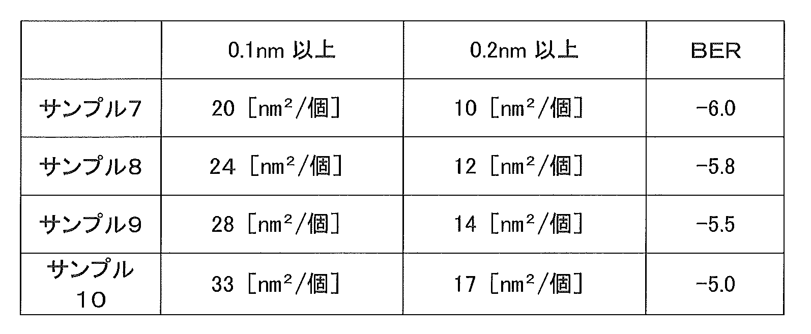
表2より、表面凹凸の平均面から0.1[nm]以上の高さを有する複数の凸部のそれぞれが占める領域の面積の平均が25[nm2/個]以下のサンプル7,8は、BERが10-5.8以下になり、磁気ディスク特性が向上することがわかる。
2 内孔
3 プローブ
4 棒状部材
10 輪郭曲線要素
12 平均線
14 レベル線
Claims (14)
- 磁気ディスク用基板であって、
前記磁気ディスク用基板は一対の主表面を有し、
前記主表面の算術平均粗さRaは、0.11nm以下であり、
前記表面粗さRaは、カーボンナノファイバの棒状部材をプローブ先端に設けたプローブを備える原子間力顕微鏡を用いて測定した値である、ことを特徴とする磁気ディスク用基板。 - 磁気ディスク用基板であって、
前記磁気ディスク用基板は一対の主表面を有し、
前記主表面の表面凹凸のうち、該表面凹凸の平均面から0.1[nm]以上の高さを有する複数の凸部のそれぞれが占める領域の面積の平均は25[nm2/個]以下であり、
前記主表面の表面凹凸は、カーボンナノファイバの棒状部材をプローブ先端に設けたプローブを備える原子間力顕微鏡を用いて測定した値である、ことを特徴とする磁気ディスク用基板。 - 前記表面凹凸の平均面から0.1[nm]以上の高さを有する複数の凸部のそれぞれが占める領域の面積の平均は20[nm2/個]以下である、請求項1または2に記載の磁気ディスク用基板。
- 前記表面凹凸の平均面から0.1[nm]以上の高さを有する複数の凸部のそれぞれが占める領域の面積の平均と、前記表面凹凸の平均面から0.2[nm]以上の高さを有する複数の凸部のそれぞれが占める領域の面積の平均との間の差は、13[nm2/個]以下である、請求項1~3のいずれか1項に記載の磁気ディスク用基板。
- 前記プローブ先端に設けられるカーボンナノファイバの棒状部材は、ヤング率が100GPa以下である、請求項1~4のいずれか1項に記載の磁気ディスク用基板。
- 前記棒状部材は導電性を有し、前記棒状部材の一方の端がアースに接続されている、請求項1~5のいずれか1項に記載の磁気ディスク用基板。
- 前記表面粗さRaあるいは前記表面凹凸は、前記プローブが一定の振幅で振動するように、前記プローブの前記主表面の表面凹凸に応じて前記プローブの位置を変化させることにより得られる、前記プローブの位置の情報から求める、請求項1~6のいずれか1項に記載の磁気ディスク用基板。
- 前記原子力顕微鏡の測定では、前記プローブを、0.1~80[N/m]のばね定数で、振動数30~400[KHz]で振動させる、請求項7に記載の磁気ディスク用基板。
- 前記基板は、エネルギーアシスト磁気記録用磁気ディスク用の基板である、請求項1~8のいずれか1項に記載の磁気ディスク用基板。
- 請求項1~9のいずれか1項に記載の前記磁気ディスク基板の表面に、少なくとも磁性膜を形成した、磁気ディスク。
- 磁気ディスク用基板の製造方法であって、
研削処理後、研磨処理工程において、カーボンナノファイバの棒状部材をプローブ先端に設けたプローブを備える原子間力顕微鏡を用いて測定した前記主表面の表面凹凸について、前記表面凹凸の平均面から0.1[nm]以上の高さを有する複数の凸部のそれぞれが占める領域の面積の平均が25[nm2/個]以下となるように前記基板の一対の主表面を30μm以下の取り代で研磨する、ことを特徴とする磁気ディスク用基板の製造方法。 - 前記研磨処理工程は、
磁気ディスク用基板の一対の主表面を酸性の研磨液を用いて第1の研磨をし、
前記第1の研磨後、ガラス基板の主表面をアルカリ性の研磨液を用いて第2の研磨をし、
前記第2の研磨では、前記第1の研磨に比べて研磨時間を短くする、ことを含む、請求項11に記載の磁気ディスク用基板の製造方法。 - 前記主表面の表面凹凸のうち、該表面凹凸の平均面から0.1[nm]以上の高さを有する複数の凸部のそれぞれが占める領域の面積の平均は20[nm2/個]以下である、請求項11または12に記載の磁気ディスク用基板の製造方法。
- 前記主表面の表面凹凸のうち、該表面凹凸の平均面から0.2[nm]以上の高さを有する複数の凸部のそれぞれが占める領域の面積の平均は12[nm2/個]以下である、請求項11~13のいずれか1項に記載の磁気ディスク用基板の製造方法。
Priority Applications (8)
| Application Number | Priority Date | Filing Date | Title |
|---|---|---|---|
| SG11201705386YA SG11201705386YA (en) | 2015-03-31 | 2016-03-31 | Magnetic-disk substrate, magnetic disk, and method for manufacturing magnetic-disk substrate |
| MYPI2017702417A MY182265A (en) | 2015-03-31 | 2016-03-31 | Magnetic disk substrate, magnetic disk, and method for manufacturing magnetic disk substrate |
| US15/545,969 US10319403B2 (en) | 2015-03-31 | 2016-03-31 | Magnetic-disk substrate, magnetic disk, and method for manufacturing magnetic-disk substrate |
| CN201680019268.7A CN107430871B (zh) | 2015-03-31 | 2016-03-31 | 磁盘用基板、磁盘、以及磁盘用基板的制造方法 |
| JP2017510181A JP6499274B2 (ja) | 2015-03-31 | 2016-03-31 | 磁気ディスク用基板、磁気ディスク、及び、磁気ディスク用基板の製造方法 |
| CN202010092798.2A CN111341353B (zh) | 2015-03-31 | 2016-03-31 | 磁盘用基板、磁盘、以及磁盘驱动装置 |
| US16/395,850 US11094345B2 (en) | 2015-03-31 | 2019-04-26 | Magnetic-disk substrate, magnetic disk, and magnetic-disk drive device |
| US17/385,787 US11682424B2 (en) | 2015-03-31 | 2021-07-26 | Magnetic-disk substrate, magnetic disk, and magnetic-disk drive device |
Applications Claiming Priority (2)
| Application Number | Priority Date | Filing Date | Title |
|---|---|---|---|
| US201562141121P | 2015-03-31 | 2015-03-31 | |
| US62/141,121 | 2015-03-31 |
Related Child Applications (2)
| Application Number | Title | Priority Date | Filing Date |
|---|---|---|---|
| US15/545,969 A-371-Of-International US10319403B2 (en) | 2015-03-31 | 2016-03-31 | Magnetic-disk substrate, magnetic disk, and method for manufacturing magnetic-disk substrate |
| US16/395,850 Continuation US11094345B2 (en) | 2015-03-31 | 2019-04-26 | Magnetic-disk substrate, magnetic disk, and magnetic-disk drive device |
Publications (1)
| Publication Number | Publication Date |
|---|---|
| WO2016159228A1 true WO2016159228A1 (ja) | 2016-10-06 |
Family
ID=57004784
Family Applications (1)
| Application Number | Title | Priority Date | Filing Date |
|---|---|---|---|
| PCT/JP2016/060647 Ceased WO2016159228A1 (ja) | 2015-03-31 | 2016-03-31 | 磁気ディスク用基板、磁気ディスク、及び、磁気ディスク用基板の製造方法 |
Country Status (6)
| Country | Link |
|---|---|
| US (3) | US10319403B2 (ja) |
| JP (2) | JP6499274B2 (ja) |
| CN (2) | CN111341353B (ja) |
| MY (1) | MY182265A (ja) |
| SG (2) | SG11201705386YA (ja) |
| WO (1) | WO2016159228A1 (ja) |
Families Citing this family (3)
| Publication number | Priority date | Publication date | Assignee | Title |
|---|---|---|---|---|
| MY182265A (en) | 2015-03-31 | 2021-01-18 | Hoya Corp | Magnetic disk substrate, magnetic disk, and method for manufacturing magnetic disk substrate |
| DE102016111909B4 (de) * | 2016-06-29 | 2020-08-13 | Infineon Technologies Ag | Mikromechanische Struktur und Verfahren zu ihrer Herstellung |
| SG11202100827XA (en) | 2018-08-07 | 2021-03-30 | Hoya Corp | Substrate for magnetic disk and magnetic disk |
Citations (6)
| Publication number | Priority date | Publication date | Assignee | Title |
|---|---|---|---|---|
| JP2004063062A (ja) * | 2002-06-05 | 2004-02-26 | Nippon Sheet Glass Co Ltd | 情報記録媒体用ガラス基板の製造方法及びその製造方法で製造された情報記録媒体用ガラス基板 |
| JP2007168057A (ja) * | 2005-12-26 | 2007-07-05 | Kao Corp | 磁気ディスク基板の製造方法 |
| WO2007109777A2 (en) * | 2006-03-22 | 2007-09-27 | Veeco Instruments Inc. | Stiffness tomography by atomic force microscopy |
| WO2009128500A1 (ja) * | 2008-04-17 | 2009-10-22 | オリンパス株式会社 | カーボンナノファイバー探針カンチレバー |
| WO2014208762A1 (ja) * | 2013-06-29 | 2014-12-31 | Hoya株式会社 | ガラス基板の製造方法及び磁気ディスクの製造方法、並びにガラス基板用研磨液組成物 |
| WO2015046603A1 (ja) * | 2013-09-30 | 2015-04-02 | Hoya株式会社 | シリカ砥粒、シリカ砥粒の製造方法および磁気ディスク用ガラス基板の製造方法 |
Family Cites Families (17)
| Publication number | Priority date | Publication date | Assignee | Title |
|---|---|---|---|---|
| US7010939B2 (en) | 2002-06-05 | 2006-03-14 | Hoya Corporation | Glass substrate for data recording medium and manufacturing method thereof |
| CN1310024C (zh) * | 2004-02-28 | 2007-04-11 | 鸿富锦精密工业(深圳)有限公司 | 原子力显微镜探针装置及其制造方法 |
| JP4452827B2 (ja) * | 2004-12-28 | 2010-04-21 | 独立行政法人産業技術総合研究所 | 走査型磁気力顕微鏡用探針およびその製造方法並びにカーボンナノチューブ用強磁性合金成膜方法 |
| DE102006039651A1 (de) * | 2005-08-31 | 2007-03-22 | Hitachi Kenki Finetech Co., Ltd. | Cantilever und Prüfvorrichtung |
| GB2433515B (en) | 2005-12-22 | 2011-05-04 | Kao Corp | Polishing composition for hard disk substrate |
| JP2008293552A (ja) | 2007-05-22 | 2008-12-04 | Fujitsu Ltd | 基板、磁気記録媒体及びその製造方法、並びに磁気記憶装置 |
| JP2009109411A (ja) * | 2007-10-31 | 2009-05-21 | Hitachi Kenki Fine Tech Co Ltd | プローブとその製造方法および走査型プローブ顕微鏡 |
| CN103151051B (zh) * | 2008-09-30 | 2015-12-09 | Hoya株式会社 | 磁盘用玻璃基板及磁盘 |
| CN102109535A (zh) * | 2009-12-24 | 2011-06-29 | 北京五泽坤科技有限公司 | 可控制备碳纳米管原子力显微镜针尖的方法 |
| SG177343A1 (en) * | 2009-12-29 | 2012-02-28 | Hoya Corp | Glass substrate for magnetic disk and manufacturing method thereof |
| KR101993322B1 (ko) * | 2011-09-28 | 2019-06-26 | 호야 가부시키가이샤 | 마스크블랭크용 유리기판, 다층 반사막 부착 기판, 마스크블랭크 및 마스크, 그리고 그것들의 제조방법 |
| CN104011795B (zh) * | 2011-12-29 | 2017-02-22 | Hoya株式会社 | 磁盘用玻璃基板的制造方法 |
| CN103293341B (zh) | 2012-02-23 | 2015-07-01 | 清华大学 | 原子力显微镜探针 |
| CN105580078B (zh) | 2013-09-28 | 2019-11-05 | Hoya株式会社 | 玻璃基板的制造方法和磁盘的制造方法 |
| KR101626936B1 (ko) * | 2014-10-10 | 2016-06-02 | 한국과학기술연구원 | 끝단이 날카로운 탄소나노섬유 및 팔라듐 촉매를 이용한 탄소나노섬유의 성장방법 |
| MY182265A (en) * | 2015-03-31 | 2021-01-18 | Hoya Corp | Magnetic disk substrate, magnetic disk, and method for manufacturing magnetic disk substrate |
| JP2018101451A (ja) | 2015-04-23 | 2018-06-28 | 旭硝子株式会社 | 磁気記録媒体用基板、磁気記録媒体、及び製造方法 |
-
2016
- 2016-03-31 MY MYPI2017702417A patent/MY182265A/en unknown
- 2016-03-31 JP JP2017510181A patent/JP6499274B2/ja active Active
- 2016-03-31 WO PCT/JP2016/060647 patent/WO2016159228A1/ja not_active Ceased
- 2016-03-31 SG SG11201705386YA patent/SG11201705386YA/en unknown
- 2016-03-31 CN CN202010092798.2A patent/CN111341353B/zh active Active
- 2016-03-31 US US15/545,969 patent/US10319403B2/en active Active
- 2016-03-31 SG SG10201912466TA patent/SG10201912466TA/en unknown
- 2016-03-31 CN CN201680019268.7A patent/CN107430871B/zh active Active
-
2019
- 2019-03-14 JP JP2019047243A patent/JP6664530B2/ja active Active
- 2019-04-26 US US16/395,850 patent/US11094345B2/en active Active
-
2021
- 2021-07-26 US US17/385,787 patent/US11682424B2/en active Active
Patent Citations (6)
| Publication number | Priority date | Publication date | Assignee | Title |
|---|---|---|---|---|
| JP2004063062A (ja) * | 2002-06-05 | 2004-02-26 | Nippon Sheet Glass Co Ltd | 情報記録媒体用ガラス基板の製造方法及びその製造方法で製造された情報記録媒体用ガラス基板 |
| JP2007168057A (ja) * | 2005-12-26 | 2007-07-05 | Kao Corp | 磁気ディスク基板の製造方法 |
| WO2007109777A2 (en) * | 2006-03-22 | 2007-09-27 | Veeco Instruments Inc. | Stiffness tomography by atomic force microscopy |
| WO2009128500A1 (ja) * | 2008-04-17 | 2009-10-22 | オリンパス株式会社 | カーボンナノファイバー探針カンチレバー |
| WO2014208762A1 (ja) * | 2013-06-29 | 2014-12-31 | Hoya株式会社 | ガラス基板の製造方法及び磁気ディスクの製造方法、並びにガラス基板用研磨液組成物 |
| WO2015046603A1 (ja) * | 2013-09-30 | 2015-04-02 | Hoya株式会社 | シリカ砥粒、シリカ砥粒の製造方法および磁気ディスク用ガラス基板の製造方法 |
Also Published As
| Publication number | Publication date |
|---|---|
| SG10201912466TA (en) | 2020-02-27 |
| CN107430871B (zh) | 2020-02-28 |
| MY182265A (en) | 2021-01-18 |
| CN111341353B (zh) | 2022-03-11 |
| CN107430871A (zh) | 2017-12-01 |
| US20210375313A1 (en) | 2021-12-02 |
| US20180005659A1 (en) | 2018-01-04 |
| US11682424B2 (en) | 2023-06-20 |
| JPWO2016159228A1 (ja) | 2017-11-30 |
| JP6499274B2 (ja) | 2019-04-10 |
| JP2019096377A (ja) | 2019-06-20 |
| SG11201705386YA (en) | 2017-08-30 |
| US20190251993A1 (en) | 2019-08-15 |
| US11094345B2 (en) | 2021-08-17 |
| JP6664530B2 (ja) | 2020-03-13 |
| CN111341353A (zh) | 2020-06-26 |
| US10319403B2 (en) | 2019-06-11 |
Similar Documents
| Publication | Publication Date | Title |
|---|---|---|
| JP6165227B2 (ja) | ガラス基板、磁気ディスク用ガラス基板の製造方法、磁気ディスク用基板、磁気ディスク、磁気ディスクの製造方法 | |
| JP6215770B2 (ja) | 磁気ディスク用ガラス基板、磁気ディスク、磁気ディスク用ガラス基板の製造方法 | |
| US11024335B2 (en) | Magnetic-disk glass substrate | |
| US11710505B2 (en) | Magnetic-disk glass substrate, magnetic-disk glass substrate intermediate, and method for manufacturing magnetic-disk glass substrate | |
| US11682424B2 (en) | Magnetic-disk substrate, magnetic disk, and magnetic-disk drive device | |
| JP6574537B2 (ja) | 磁気ディスク用非磁性基板及び磁気ディスク | |
| JP4748115B2 (ja) | 磁気記録媒体用ガラス基板及び磁気記録媒体 | |
| JP5714085B2 (ja) | 磁気ディスク用基板および磁気ディスク | |
| CN105164751B (zh) | 圆盘状玻璃基板、磁盘用玻璃基板、磁盘用玻璃基板的制造方法及磁盘 | |
| JP4631971B2 (ja) | ガラス基板の製造方法および磁気ディスクの製造方法 | |
| JP2014041696A (ja) | 磁気ディスク用基板および磁気ディスク | |
| CN104584128B (zh) | 信息记录介质用玻璃基板的制造方法 | |
| JP5234740B2 (ja) | 磁気ディスク用基板の製造方法および磁気ディスクの製造方法 | |
| JP2015064915A (ja) | 情報記録媒体用ガラス基板の製造方法 |
Legal Events
| Date | Code | Title | Description |
|---|---|---|---|
| 121 | Ep: the epo has been informed by wipo that ep was designated in this application |
Ref document number: 16773108 Country of ref document: EP Kind code of ref document: A1 |
|
| WWE | Wipo information: entry into national phase |
Ref document number: 11201705386Y Country of ref document: SG |
|
| WWE | Wipo information: entry into national phase |
Ref document number: 15545969 Country of ref document: US |
|
| ENP | Entry into the national phase |
Ref document number: 2017510181 Country of ref document: JP Kind code of ref document: A |
|
| NENP | Non-entry into the national phase |
Ref country code: DE |
|
| 122 | Ep: pct application non-entry in european phase |
Ref document number: 16773108 Country of ref document: EP Kind code of ref document: A1 |