WO2016158952A1 - カードリーダ - Google Patents
カードリーダ Download PDFInfo
- Publication number
- WO2016158952A1 WO2016158952A1 PCT/JP2016/060130 JP2016060130W WO2016158952A1 WO 2016158952 A1 WO2016158952 A1 WO 2016158952A1 JP 2016060130 W JP2016060130 W JP 2016060130W WO 2016158952 A1 WO2016158952 A1 WO 2016158952A1
- Authority
- WO
- WIPO (PCT)
- Prior art keywords
- resistor
- card
- magnetic
- recorded
- data
- Prior art date
- Legal status (The legal status is an assumption and is not a legal conclusion. Google has not performed a legal analysis and makes no representation as to the accuracy of the status listed.)
- Ceased
Links
Images


Classifications
-
- G—PHYSICS
- G06—COMPUTING OR CALCULATING; COUNTING
- G06K—GRAPHICAL DATA READING; PRESENTATION OF DATA; RECORD CARRIERS; HANDLING RECORD CARRIERS
- G06K7/00—Methods or arrangements for sensing record carriers, e.g. for reading patterns
- G06K7/08—Methods or arrangements for sensing record carriers, e.g. for reading patterns by means detecting the change of an electrostatic or magnetic field, e.g. by detecting change of capacitance between electrodes
- G06K7/082—Methods or arrangements for sensing record carriers, e.g. for reading patterns by means detecting the change of an electrostatic or magnetic field, e.g. by detecting change of capacitance between electrodes using inductive or magnetic sensors
- G06K7/087—Methods or arrangements for sensing record carriers, e.g. for reading patterns by means detecting the change of an electrostatic or magnetic field, e.g. by detecting change of capacitance between electrodes using inductive or magnetic sensors flux-sensitive, e.g. magnetic, detectors
-
- G—PHYSICS
- G06—COMPUTING OR CALCULATING; COUNTING
- G06K—GRAPHICAL DATA READING; PRESENTATION OF DATA; RECORD CARRIERS; HANDLING RECORD CARRIERS
- G06K19/00—Record carriers for use with machines and with at least a part designed to carry digital markings
- G06K19/06—Record carriers for use with machines and with at least a part designed to carry digital markings characterised by the kind of the digital marking, e.g. shape, nature, code
- G06K19/067—Record carriers with conductive marks, printed circuits or semiconductor circuit elements, e.g. credit or identity cards also with resonating or responding marks without active components
- G06K19/07—Record carriers with conductive marks, printed circuits or semiconductor circuit elements, e.g. credit or identity cards also with resonating or responding marks without active components with integrated circuit chips
- G06K19/073—Special arrangements for circuits, e.g. for protecting identification code in memory
-
- G—PHYSICS
- G06—COMPUTING OR CALCULATING; COUNTING
- G06K—GRAPHICAL DATA READING; PRESENTATION OF DATA; RECORD CARRIERS; HANDLING RECORD CARRIERS
- G06K7/00—Methods or arrangements for sensing record carriers, e.g. for reading patterns
- G06K7/10—Methods or arrangements for sensing record carriers, e.g. for reading patterns by electromagnetic radiation, e.g. optical sensing; by corpuscular radiation
Definitions
- the present invention relates to a card reader that reads magnetic data recorded on a card and records magnetic data on the card.
- skimming magnetic head a card reader that generates a disturbing magnetic field for preventing reading of magnetic data by a magnetic head for skimming (hereinafter referred to as “skimming magnetic head”) has been proposed (for example, see Patent Document 1). .
- the card reader described in Patent Document 1 includes a disturbing magnetic field generator that generates a disturbing magnetic field, a transport roller that transports a card inserted from a card insertion slot, and a motor that drives the transport roller.
- the card reader also includes a magnetic head (pre-head) for detecting whether or not magnetic data is recorded on the magnetic stripe of the card inserted from the card insertion slot.
- pre-head detects that magnetic data is recorded on the magnetic stripe of the card inserted from the card insertion slot
- the motor starts and the transport roller takes the card into the card reader.
- the disturbing magnetic field generator generates the disturbing magnetic field while the rear end of the card protrudes from the card insertion slot after the motor is started.
- the disturbing magnetic field generator is configured to prevent disturbing magnetic fields before the magnetic stripe of the card inserted from the card insertion slot reaches the pre-head. It is preferable that the disturbing magnetic field generator generates the disturbing magnetic field for a predetermined time after the magnetic stripe reaches the pre-head. That is, in the card reader described in Patent Document 1, in order to reliably prevent skimming by the skimming magnetic head, it is preferable that a disturbing magnetic field is generated even when magnetic data is read by the prehead.
- an object of the present invention is to appropriately detect whether or not magnetic data is recorded on the magnetic stripe of the card inserted from the card insertion slot even when the disturbing magnetic field is generated. It is to provide a possible card reader.
- a card reader includes a card insertion slot into which a card having a magnetic stripe is inserted, an MR sensor for detecting whether magnetic data is recorded in the magnetic stripe, and And a disturbing magnetic field generating means for generating a disturbing magnetic field for preventing unauthorized reading of magnetic data recorded on the magnetic stripe, and the magnetic stripe is arranged in the moving direction of the card inserted from the card insertion slot.
- the MR sensor includes a first resistor disposed in a distance less than a bit interval of magnetic data when 0 data is recorded on the magnetic stripe in the card moving direction, A second resistor is provided.
- the MR sensor for detecting whether or not magnetic data is recorded in the magnetic stripe includes the first resistor and the second resistor.
- the first resistor and the second resistor are the bit interval of magnetic data when 0 data is recorded on the magnetic stripe in the card moving direction that coincides with the arrangement direction of the magnetic data.
- the distance between the first resistor and the second resistor in the moving direction of the card is very close. Therefore, in the present invention, it is possible to suppress the difference between the resistance change amount of the first resistor and the resistance change amount of the second resistor caused by the disturbing magnetic field generated by the disturbing magnetic field generating means. Become.
- the difference between the resistance change amount of the first resistor and the resistance change amount of the second resistor due to the magnetic data recorded in the magnetic stripe It becomes possible to enlarge. Therefore, in the present invention, even when the disturbing magnetic field is generated, the card insertion slot is based on the difference between the resistance change amount of the first resistor and the resistance change amount of the second resistor. It is possible to appropriately detect whether or not magnetic data is recorded on the magnetic stripe of the card inserted from.
- the first resistor and the second resistor are arranged at a distance of half the bit interval of magnetic data when 0 data is recorded on the magnetic stripe in the card moving direction.
- the international standard and JIS standard stipulate that 0 data is recorded in the preamble on the leading end of the magnetic stripe. If configured in this way, the magnetic data is recorded on the magnetic stripe of a card conforming to the international standard or JIS standard. Is recorded, it becomes possible to further increase the difference between the amount of change in resistance of the first resistor and the amount of change in resistance of the second resistor due to the magnetic data. Therefore, it is possible to more appropriately detect whether magnetic data is recorded in the magnetic stripe based on the difference between the resistance change amount of the first resistor and the resistance change amount of the second resistor. Is possible.
- the first resistor and the second resistor are connected in series, and one of the first resistor and the second resistor is connected to the power source, and the first resistor and the second resistor Preferably, the other of the two resistors is grounded, and the potential at the midpoint between the first resistor and the second resistor is the output of the MR sensor.
- the difference between the resistance change amount of the first resistor and the resistance change amount of the second resistor becomes the output of the MR sensor as it is, for example, the first resistor and the first resistor Compared with the case where the two resistors are connected in parallel, the processing of the output signal of the MR sensor becomes easier.
- the MR sensor includes a plurality of sets of first resistors and second resistors, and the MR sensor records whether or not magnetic data is recorded for each track recorded in the magnetic stripe. It is preferable to detect. If comprised in this way, it will become possible to detect more appropriately whether the magnetic data of several tracks are recorded on the magnetic stripe.
- the card reader according to the present invention appropriately determines whether or not magnetic data is recorded on the magnetic stripe of the card inserted from the card insertion slot even when the disturbing magnetic field is generated. It becomes possible to detect.
- FIG. 1 It is a schematic diagram of a card reader concerning an embodiment of the invention. It is a figure which shows the back surface of the card
- FIG. 1 is a schematic diagram of a card reader 1 according to an embodiment of the present invention.
- FIG. 2 is a view showing the back surface of the card 2 shown in FIG.
- the card reader 1 of this embodiment is a device for reading magnetic data recorded on the card 2 and recording magnetic data on the card 2, and is used by being mounted on a predetermined host device such as an ATM.
- the card reader 1 includes a card insertion portion 4 in which a card insertion slot 3 into which a card 2 is inserted is formed, and a main body portion 5.
- a card passage 6 through which the card 2 inserted from the card insertion slot 3 passes is formed inside the card reader 1.
- the card 2 inserted from the card insertion slot 3 moves in the X direction shown in FIG. That is, the X direction is the moving direction of the card 2. Further, the Z direction in FIG. 1 orthogonal to the X direction is the thickness direction of the card 2 taken into the card reader 1, and the Y direction in FIG. 1 orthogonal to the X direction and the Z direction is to the card reader 1. This is the width direction of the captured card 2.
- Card 2 is a substantially rectangular vinyl chloride card having a thickness of about 0.7 to 0.8 mm.
- a magnetic stripe 2a for recording magnetic data is formed on the back surface of the card 2.
- the magnetic stripe 2a is formed along the longitudinal direction of the card 2 formed in a substantially rectangular shape.
- Magnetic data arranged in the longitudinal direction of the magnetic stripe 2a (that is, the longitudinal direction of the card 2) is recorded on the magnetic stripe 2a.
- the card 2 of this embodiment is a card conforming to international standards and JIS standards, and “0” data is recorded in the preamble on the leading end side of the magnetic stripe 2a.
- the card 2 is inserted into the card reader 1 with its back side facing downward and the longitudinal direction of the card 2 substantially coincides with the X direction (the moving direction of the card 2). Move in. That is, the magnetic data recorded on the magnetic stripe 2 a is arranged in the moving direction of the card 2.
- the card 2 may incorporate an IC chip or a communication antenna.
- the card 2 may be a PET (polyethylene terephthalate) card having a thickness of about 0.18 to 0.36 mm, or a paper card having a predetermined thickness.
- the card reader 1 conveys the card 2 in the card passage 6 with a magnetic head 7 for reading the magnetic data recorded on the magnetic stripe 2 a of the card 2 and recording the magnetic data on the magnetic stripe 2 a.
- Drive roller 8 and pad roller 9 MR sensor 10 for detecting whether or not magnetic data is recorded on magnetic stripe 2 a, and preventing unauthorized reading of magnetic data recorded on magnetic stripe 2 a
- a disturbing magnetic field generating means 11 for generating a magnetic field (disturbing magnetic field).
- the magnetic head 7, the driving roller 8 and the pad roller 9 are arranged in the main body 5.
- the MR sensor 10 and the disturbing magnetic field generating means 11 are arranged in the card insertion part 4.
- the magnetic head 7 is disposed so as to face the card passage 6 from below.
- the magnetic head 7 is disposed at a position where the magnetic stripe 2a passes in the Y direction.
- the drive roller 8 and the pad roller 9 are disposed so as to face each other in the vertical direction.
- the pad roller 9 is urged toward the driving roller 8.
- the MR sensor 10 is arranged so as to face the card passage 6 from below. A specific configuration of the MR sensor 10 will be described later.
- the disturbing magnetic field generating means 11 includes a core formed of a magnetic material and an exciting coil wound around the core.
- the core and the coil are disposed on the upper side of the card passage 6.
- the coil is connected to an AC power supply circuit that supplies current to the coil. When current is supplied to the coil, the magnetic field is disturbed toward the front of the card reader 1 and toward the position where the magnetic stripe 2a passes. Will occur.
- the core and the coil may be disposed below the card passage 6.
- the disturbing magnetic field generating means 11 When the card reader 1 detects that the card 2 is inserted into the card insertion slot 3 by a card insertion detection mechanism (not shown), the disturbing magnetic field generating means 11 generates a disturbing magnetic field and the MR sensor 10 is powered. Is supplied.
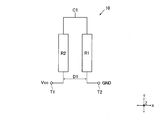
- FIG. 3 is a diagram for explaining the configuration of the MR sensor 10 shown in FIG.
- the MR sensor 10 includes a first resistor R1 (hereinafter referred to as a resistor R1) and a second resistor R2 connected in series as MR elements (magnetoresistance effect elements). (Hereinafter referred to as resistor R2).
- the resistors R1 and R2 are formed of, for example, a nickel iron alloy thin film.
- the resistors R1 and R2 are formed by being folded back multiple times in the Y direction (short direction of the card 2).
- the resistors R1 and R2 are formed by being folded twice in the Y direction.
- the resistors R1 and R2 are formed in a straight line parallel to the Y direction.
- the resistors R1 and R2 may be formed of a material other than the nickel iron alloy.
- the resistor R2 is connected to the power source Vcc. Specifically, one end of the resistor R2 not connected to the resistor R1 is connected to the connection terminal T1 to the power supply Vcc, and the connection terminal T1 is connected to the power supply Vcc.
- the resistor R1 is grounded. Specifically, one end of the resistor R1 that is not connected to the resistor R2 is connected to the grounding terminal T2, and the grounding terminal T2 is grounded. Further, the potential of the midpoint C1 between the resistor R1 and the resistor R2 connected in series (the connection point between the resistor R1 and the resistor R2) is the output of the MR sensor 10.
- the resistance value of the resistor R1 is equal to the resistance value of the resistor R2.
- the length of the resistor R1 in the Y direction is equal to the length of the resistor R2 in the Y direction. Further, this length is narrower than the width in the Y direction of the magnetic data recorded on the magnetic stripe 2a. For example, this length is 2 mm.
- the width of the resistor R1 in the X direction is equal to the width of the resistor portion R2 in the X direction. For example, this width is 60 ⁇ m.
- the film thickness of the resistor R1 is equal to the film thickness of the resistor R2. For example, this film thickness is 45 nm.
- Resistor R1 and resistor R2 are arranged at the same position in the Y direction. Specifically, the resistor R1 and the resistor R2 are arranged at a position where the magnetic stripe 2a passes in the Y direction. Further, the resistor R1 and the resistor R2 are arranged in a state of being separated by a distance D1 in the X direction. The distance D1 is less than the maximum bit interval of the magnetic data recorded on the magnetic stripe 2a. That is, the distance D1 is less than the bit interval of the magnetic data when “0” data is recorded in the magnetic stripe 2a.
- the distance D1 is half the bit interval of the magnetic data when “0” data is recorded in the magnetic stripe 2a. That is, the distance D1 is the same distance as the bit interval of magnetic data when “1” data is recorded in the magnetic stripe 2a.
- the distance D1 is equal to the portion of the resistor R1 disposed closest to the resistor R2 and the resistor R2. This is the distance from the portion arranged closest to the resistor R1.
- the resistor R1 and the resistor R2 are arranged in the state of being separated by the distance D1 in the X direction, and “0” data is recorded on the magnetic stripe 2a.
- the distance is half the bit interval of the magnetic data. That is, in this embodiment, the distance between the resistor R1 and the resistor R2 in the X direction is very short. Therefore, in this embodiment, the difference between the resistance change amount of the resistor R1 and the resistance change amount of the resistor R2 due to the disturbing magnetic field generated by the disturbing magnetic field generation unit 11 can be suppressed to be small.
- the distance D1 between the resistor R1 and the resistor R2 in the X direction is half the bit interval of magnetic data when “0” data is recorded in the magnetic stripe 2a.
- the difference between the resistance change amount of the resistor R1 and the resistance change amount of the resistor R2 due to the “0” data recorded in the magnetic stripe 2a can be increased.
- the resistance value of the resistor R1 and the resistance value of the resistor R2 are equal, and the potential at the midpoint C1 between the resistor R1 and the resistor R2 becomes the output of the MR sensor 10. ing.
- the card insertion detecting mechanism (not shown) detects that the card 2 is inserted into the card insertion slot 3
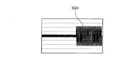
- the disturbing magnetic field generating means 11 generates a disturbing magnetic field and the MR sensor 10 Power is supplied. Therefore, in this embodiment, when magnetic data is recorded on the magnetic stripe 2a of the card 2 inserted into the card insertion slot 3, when the card 2 moves to the back side of the card reader 1, the MR sensor 10
- the output signal SG1 changes as shown in FIG.
- the amplitude of the output signal SG1 is very high until the magnetic data recording area of the magnetic stripe 2a reaches the MR sensor 10 (until the preamble of the magnetic stripe 2a reaches the MR sensor 10).
- the amplitude of the output signal SG1 increases. Therefore, in this embodiment, whether or not magnetic data is recorded on the magnetic stripe 2a of the card 2 inserted from the card insertion slot 3 is properly determined by the MR sensor 10 even in the state where the disturbing magnetic field is generated. Can be detected.
- the resistor R1 and the resistor R2 are connected in series, but the resistor R1 and the resistor R2 may be connected in parallel.
- the difference between the resistance change amount of the resistor R1 and the resistance change amount of the resistor R2 is calculated by a predetermined circuit to detect whether magnetic data is recorded in the magnetic stripe 2a. Just do it.
- the resistor R1 and the resistor R2 are connected in series as in the above-described embodiment, the difference between the resistance change amount of the resistor R1 and the resistance change amount of the resistor R2 can be obtained without changing the MR. Since it becomes possible to make it the output of the sensor 10, the process of the output signal of the MR sensor 10 becomes easy compared with the case where the resistor R1 and the resistor R2 are connected in parallel.
- the distance D1 between the resistor R1 and the resistor R2 is half the bit interval of magnetic data when “0” data is recorded in the magnetic stripe 2a.
- the distance D1 is less than the bit interval of the magnetic data when the “0” data is recorded in the magnetic stripe 2a, the “0” data is recorded in the magnetic data.
- the distance may be a distance other than half the bit interval of the magnetic data.
- the MR sensor 10 includes a plurality of sets of first resistors and second resistors for detecting whether or not magnetic data is recorded for each track.
- the magnetic data of two tracks that is, the magnetic data of the first track and the magnetic data of the second track may be recorded on the magnetic stripe 2a.
- the MR sensor 10 records the first resistor and the second resistor for detecting whether or not magnetic data is recorded on the first track, and the magnetic data is recorded on the second track.
- a first resistor and a second resistor for detecting whether or not the device is being used.
- the first resistor and the second resistor for detecting whether or not magnetic data is recorded on the first track are the same as the resistors R1 and R2 in the above-described form.
- the first resistor and the second resistor for detecting whether or not magnetic data is recorded on the second track are also configured in the same manner as the resistors R1 and R2 of the above-described form. ing.
- the distance in the X direction between the first resistor and the second resistor for detecting whether or not magnetic data is recorded in the first track is, for example, “0” data in the first track.
- the first resistor and the second resistor for detecting whether or not the magnetic data is recorded on the second track which is half the distance of the bit interval of the magnetic data when is recorded
- the distance in the X direction is, for example, a half of the bit interval of magnetic data when “0” data is recorded on the second track.
- the card reader 1 is a card transport type card reader having the driving roller 8 and the pad roller 9.
- the card reader 1 may be a manual card reader that is manually operated by the user. good.
Landscapes
- Engineering & Computer Science (AREA)
- Physics & Mathematics (AREA)
- Theoretical Computer Science (AREA)
- General Physics & Mathematics (AREA)
- Computer Vision & Pattern Recognition (AREA)
- Artificial Intelligence (AREA)
- Computer Hardware Design (AREA)
- Microelectronics & Electronic Packaging (AREA)
- General Engineering & Computer Science (AREA)
- Computer Security & Cryptography (AREA)
- Health & Medical Sciences (AREA)
- Electromagnetism (AREA)
- General Health & Medical Sciences (AREA)
- Toxicology (AREA)
- Recording Or Reproducing By Magnetic Means (AREA)
Priority Applications (3)
| Application Number | Priority Date | Filing Date | Title |
|---|---|---|---|
| EP16772833.6A EP3279828B1 (en) | 2015-03-30 | 2016-03-29 | Card reader |
| US15/563,091 US10055615B2 (en) | 2015-03-30 | 2016-03-29 | Card reader |
| CN201680019128.XA CN107430674B (zh) | 2015-03-30 | 2016-03-29 | 读卡器 |
Applications Claiming Priority (2)
| Application Number | Priority Date | Filing Date | Title |
|---|---|---|---|
| JP2015067983A JP2016189055A (ja) | 2015-03-30 | 2015-03-30 | カードリーダ |
| JP2015-067983 | 2015-03-30 |
Publications (1)
| Publication Number | Publication Date |
|---|---|
| WO2016158952A1 true WO2016158952A1 (ja) | 2016-10-06 |
Family
ID=57005951
Family Applications (1)
| Application Number | Title | Priority Date | Filing Date |
|---|---|---|---|
| PCT/JP2016/060130 Ceased WO2016158952A1 (ja) | 2015-03-30 | 2016-03-29 | カードリーダ |
Country Status (5)
| Country | Link |
|---|---|
| US (1) | US10055615B2 (enExample) |
| EP (1) | EP3279828B1 (enExample) |
| JP (1) | JP2016189055A (enExample) |
| CN (1) | CN107430674B (enExample) |
| WO (1) | WO2016158952A1 (enExample) |
Families Citing this family (4)
| Publication number | Priority date | Publication date | Assignee | Title |
|---|---|---|---|---|
| JP7085814B2 (ja) * | 2017-08-31 | 2022-06-17 | 日本電産サンキョー株式会社 | カードリーダ |
| US10496914B2 (en) | 2017-10-31 | 2019-12-03 | University Of Florida Research Foundation, Incorporated | Payment card overlay skimmer detection |
| JP2020113357A (ja) * | 2019-01-17 | 2020-07-27 | 日本電産サンキョー株式会社 | 磁気記録媒体処理装置および制御方法 |
| CN112085905B (zh) * | 2019-06-14 | 2022-03-01 | 中电金融设备系统(深圳)有限公司 | 磁条卡阅读器、磁条数据处理装置及磁条数据处理方法 |
Citations (4)
| Publication number | Priority date | Publication date | Assignee | Title |
|---|---|---|---|---|
| JPS58129585A (ja) * | 1982-01-27 | 1983-08-02 | Denki Onkyo Co Ltd | 磁気抵抗素子を用いたパタ−ン認識装置 |
| JPH05314313A (ja) * | 1991-10-01 | 1993-11-26 | Ncr Internatl Inc | 磁気インク文字読取り用磁気抵抗ヘッド |
| JPH11510299A (ja) * | 1995-08-07 | 1999-09-07 | マグネティック・プロダクツ・インターナショナル・コーポレーション | セキュリティ機能付クレジット・カード |
| WO2012085967A1 (ja) * | 2010-12-22 | 2012-06-28 | 日立オムロンターミナルソリューションズ株式会社 | 磁気記録媒体読取装置 |
Family Cites Families (12)
| Publication number | Priority date | Publication date | Assignee | Title |
|---|---|---|---|---|
| JPH08145718A (ja) * | 1994-11-17 | 1996-06-07 | Canon Electron Inc | 磁気抵抗効果センサ |
| JPH097119A (ja) * | 1995-06-19 | 1997-01-10 | Oki Electric Ind Co Ltd | 磁気ヘッドアレイおよびその製造方法 |
| JP3936496B2 (ja) * | 1999-08-31 | 2007-06-27 | 日本電産サンキョー株式会社 | 磁気カード取引装置 |
| US20080290167A1 (en) * | 2007-05-24 | 2008-11-27 | Clay Von Mueller | Multi dimensional read head array |
| JP5728791B2 (ja) * | 2009-03-05 | 2015-06-03 | 日本電産サンキョー株式会社 | カードリーダ |
| JP5759807B2 (ja) * | 2011-06-29 | 2015-08-05 | 日本電産サンキョー株式会社 | カード挿入部およびカードリーダ |
| EP2752825B1 (en) * | 2011-08-30 | 2017-03-22 | Hitachi-Omron Terminal Solutions, Corporation | Device for reading magnetic recording medium |
| JP5759552B2 (ja) * | 2011-08-30 | 2015-08-05 | 日立オムロンターミナルソリューションズ株式会社 | 磁気記録媒体読取装置 |
| WO2013118183A1 (ja) * | 2012-02-09 | 2013-08-15 | 日立オムロンターミナルソリューションズ株式会社 | 磁気カード読取装置および磁気カード読取方法 |
| JP5648024B2 (ja) * | 2012-07-10 | 2015-01-07 | 日本電産サンキョー株式会社 | カードリーダ |
| WO2014195991A1 (ja) * | 2013-06-04 | 2014-12-11 | 日立オムロンターミナルソリューションズ株式会社 | 磁気記録媒体読取装置 |
| DE102014119663A1 (de) * | 2014-12-29 | 2016-06-30 | Infineon Technologies Ag | Chipkarte |
-
2015
- 2015-03-30 JP JP2015067983A patent/JP2016189055A/ja active Pending
-
2016
- 2016-03-29 CN CN201680019128.XA patent/CN107430674B/zh active Active
- 2016-03-29 WO PCT/JP2016/060130 patent/WO2016158952A1/ja not_active Ceased
- 2016-03-29 US US15/563,091 patent/US10055615B2/en active Active
- 2016-03-29 EP EP16772833.6A patent/EP3279828B1/en active Active
Patent Citations (4)
| Publication number | Priority date | Publication date | Assignee | Title |
|---|---|---|---|---|
| JPS58129585A (ja) * | 1982-01-27 | 1983-08-02 | Denki Onkyo Co Ltd | 磁気抵抗素子を用いたパタ−ン認識装置 |
| JPH05314313A (ja) * | 1991-10-01 | 1993-11-26 | Ncr Internatl Inc | 磁気インク文字読取り用磁気抵抗ヘッド |
| JPH11510299A (ja) * | 1995-08-07 | 1999-09-07 | マグネティック・プロダクツ・インターナショナル・コーポレーション | セキュリティ機能付クレジット・カード |
| WO2012085967A1 (ja) * | 2010-12-22 | 2012-06-28 | 日立オムロンターミナルソリューションズ株式会社 | 磁気記録媒体読取装置 |
Non-Patent Citations (1)
| Title |
|---|
| See also references of EP3279828A4 * |
Also Published As
| Publication number | Publication date |
|---|---|
| JP2016189055A (ja) | 2016-11-04 |
| CN107430674B (zh) | 2020-03-27 |
| EP3279828A1 (en) | 2018-02-07 |
| EP3279828B1 (en) | 2019-10-30 |
| EP3279828A4 (en) | 2018-11-07 |
| US20180075263A1 (en) | 2018-03-15 |
| US10055615B2 (en) | 2018-08-21 |
| CN107430674A (zh) | 2017-12-01 |
Similar Documents
| Publication | Publication Date | Title |
|---|---|---|
| US8985450B2 (en) | Card insertion part and card reader | |
| US8824073B2 (en) | Card reader and control method of card reader | |
| JP6461670B2 (ja) | カードリーダおよびカードリーダの制御方法 | |
| US9626820B2 (en) | Card reader | |
| US20070023532A1 (en) | Electronic stripe cards | |
| CN102982613A (zh) | 磁读取装置 | |
| CN106471519B (zh) | 读卡器 | |
| WO2016158952A1 (ja) | カードリーダ | |
| US10902225B2 (en) | Card reader | |
| US10043044B2 (en) | Card reader | |
| JP6370173B2 (ja) | Mrセンサおよびカードリーダ | |
| JP4818792B2 (ja) | 磁気検出素子及びそれを用いた磁気識別センサ | |
| JP2019061398A (ja) | 磁気センサユニットおよびカードリーダ | |
| JP2019102107A (ja) | カードリーダおよびカードリーダの制御方法 | |
| JP2019185837A (ja) | カードリーダ | |
| JP2019149215A (ja) | カードリーダ | |
| JP2019100730A (ja) | カードリーダおよびカードリーダの制御方法 |
Legal Events
| Date | Code | Title | Description |
|---|---|---|---|
| 121 | Ep: the epo has been informed by wipo that ep was designated in this application |
Ref document number: 16772833 Country of ref document: EP Kind code of ref document: A1 |
|
| WWE | Wipo information: entry into national phase |
Ref document number: 15563091 Country of ref document: US |
|
| NENP | Non-entry into the national phase |
Ref country code: DE |
|
| REEP | Request for entry into the european phase |
Ref document number: 2016772833 Country of ref document: EP |