EP3279828B1 - Card reader - Google Patents
Card reader Download PDFInfo
- Publication number
- EP3279828B1 EP3279828B1 EP16772833.6A EP16772833A EP3279828B1 EP 3279828 B1 EP3279828 B1 EP 3279828B1 EP 16772833 A EP16772833 A EP 16772833A EP 3279828 B1 EP3279828 B1 EP 3279828B1
- Authority
- EP
- European Patent Office
- Prior art keywords
- resistor
- card
- magnetic
- recorded
- magnetic stripe
- Prior art date
- Legal status (The legal status is an assumption and is not a legal conclusion. Google has not performed a legal analysis and makes no representation as to the accuracy of the status listed.)
- Active
Links
Images

Classifications
-
- G—PHYSICS
- G06—COMPUTING; CALCULATING OR COUNTING
- G06K—GRAPHICAL DATA READING; PRESENTATION OF DATA; RECORD CARRIERS; HANDLING RECORD CARRIERS
- G06K7/00—Methods or arrangements for sensing record carriers, e.g. for reading patterns
- G06K7/08—Methods or arrangements for sensing record carriers, e.g. for reading patterns by means detecting the change of an electrostatic or magnetic field, e.g. by detecting change of capacitance between electrodes
- G06K7/082—Methods or arrangements for sensing record carriers, e.g. for reading patterns by means detecting the change of an electrostatic or magnetic field, e.g. by detecting change of capacitance between electrodes using inductive or magnetic sensors
- G06K7/087—Methods or arrangements for sensing record carriers, e.g. for reading patterns by means detecting the change of an electrostatic or magnetic field, e.g. by detecting change of capacitance between electrodes using inductive or magnetic sensors flux-sensitive, e.g. magnetic, detectors
-
- G—PHYSICS
- G06—COMPUTING; CALCULATING OR COUNTING
- G06K—GRAPHICAL DATA READING; PRESENTATION OF DATA; RECORD CARRIERS; HANDLING RECORD CARRIERS
- G06K19/00—Record carriers for use with machines and with at least a part designed to carry digital markings
- G06K19/06—Record carriers for use with machines and with at least a part designed to carry digital markings characterised by the kind of the digital marking, e.g. shape, nature, code
- G06K19/067—Record carriers with conductive marks, printed circuits or semiconductor circuit elements, e.g. credit or identity cards also with resonating or responding marks without active components
- G06K19/07—Record carriers with conductive marks, printed circuits or semiconductor circuit elements, e.g. credit or identity cards also with resonating or responding marks without active components with integrated circuit chips
- G06K19/073—Special arrangements for circuits, e.g. for protecting identification code in memory
-
- G—PHYSICS
- G06—COMPUTING; CALCULATING OR COUNTING
- G06K—GRAPHICAL DATA READING; PRESENTATION OF DATA; RECORD CARRIERS; HANDLING RECORD CARRIERS
- G06K7/00—Methods or arrangements for sensing record carriers, e.g. for reading patterns
- G06K7/10—Methods or arrangements for sensing record carriers, e.g. for reading patterns by electromagnetic radiation, e.g. optical sensing; by corpuscular radiation
Definitions
- At least an embodiment of the present invention relates to a card reader structured to perform reading of magnetic data recorded in a card and recording of magnetic data to the card.
- a card reader has been widely utilized, which performs reading of magnetic data recorded in a card and recording of magnetic data to the card.
- an industry such as a financial institution where a card reader is utilized
- illegal acquisition of magnetic data of a card by a fraudulent person who attaches a magnetic head to a card insertion part of a card reader in other words, so-called skimming has conventionally become a large issue.
- a card reader has been proposed, which generates a disturbing magnetic field for preventing reading of magnetic data using a magnetic head for skimming (hereinafter, referred to as a "skimming magnetic head”) (see, for example, Patent Literature 1).
- a card reader described in Patent Literature 1 includes: a disturbing magnetic field generator that generates a disturbing magnetic field; a conveying roller that conveys a card inserted through a card insertion port; and a motor that drives the conveying roller.
- the card reader also includes a magnetic head (pre-head) that detects whether magnetic data are recorded in a magnetic stripe of the card inserted through the card insertion port.
- pre-head detects whether magnetic data are recorded in a magnetic stripe of the card inserted through the card insertion port.
- the motor is activated to drive the conveying roller. The card is thus taken into the card reader.
- the disturbing magnetic field generator after the activation of the motor, the disturbing magnetic field generator generates a disturbing magnetic field during a period of time in which a rear end side of the card is protruded from the card insertion port.
- Patent Literature 1 Japanese Patent No. 3936496
- the disturbing magnetic field generator generates a disturbing magnetic field before the magnetic stripe of the card inserted through the card insertion port reaches the pre-head and, further, the disturbing magnetic field generator generates a disturbing magnetic field for a predetermined period of time after the magnetic stripe has reached the pre-head.
- a disturbing magnetic field is also generated at the time when the pre-head reads magnetic data.
- At least an embodiment of the present invention provides a card reader capable of appropriately detecting whether magnetic data are recorded in a magnetic stripe of a card inserted through a card insertion port, even in a state in which a disturbing magnetic field is generated.
- the MR sensor for detecting whether magnetic data are recorded in a magnetic stripe includes the first resistor and the second resistor.
- the first resistor and the second resistor are disposed to be separated by the distance which is less than the bit interval of the magnetic data in the case that the "0" data are recorded in the magnetic stripe, from each other in the moving direction of the card, the moving direction being coincided with the arranging direction of the magnetic data. In other words, the distance between the first resistor and the second resistor is very short in the moving direction of the card.
- the present invention therefore, it is possible to narrow a difference between an amount of change in resistance of the first resistor and an amount of change in resistance of the second resistor, the difference being caused owing to a disturbing magnetic field generated by the disturbing magnetic field generating means.
- the first resistor and the second resistor are disposed to be separated by the distance which is less than the bit interval of the magnetic data in the case that the "0" data are recorded in the magnetic stripe, from each other in the moving direction of the card, the moving direction being coincided with the arranging direction of the magnetic data.
- the first resistor and the second resistor are disposed to be separated by a distance which is a half of the bit interval of the magnetic data in the case that the "0" data are recorded in the magnetic stripe, from each other in the moving direction of the card.
- the international standard or JIS standard specifies that "0" data are recorded in a preamble on a tip end side of a magnetic stripe.
- the first resistor and the second resistor are connected in series, one of the first resistor and the second resistor is connected to a power supply, the other one of the first resistor and the second resistor is grounded, and the MR sensor outputs a potential at a midpoint between the first resistor and the second resistor.
- the MR sensor outputs the difference between the amount of change in resistance of the first resistor and the amount of change in resistance of the second resistor as it is. Therefore, the output signal from the MR sensor can be processed with ease as compared with, for example, a case that the first resistor and the second resistor are connected in parallel.
- the MR sensor includes multiple sets of first resistors and multiple sets of second resistors, and the MR sensor detects whether magnetic data are recorded, for each track to be recorded in the magnetic stripe.
- the MR sensor detects whether magnetic data are recorded, for each track to be recorded in the magnetic stripe.
- a card reader is capable of appropriately detecting whether magnetic data are recorded in a magnetic stripe of a card inserted through a card insertion port, even in a state in which a disturbing magnetic field is generated.
- FIG. 1 is a schematic view showing a card reader 1 in accordance with an embodiment of the present invention.
- FIG. 2 is a view showing a rear face of a card 2 shown in FIG. 1 .
- the card reader 1 in this embodiment is a device for performing reading of magnetic data recorded in the card 2 and recording of magnetic data to the card 2 and is mounted for use on a predetermined host apparatus such as an automated teller machine (ATM).
- the card reader 1 includes a card insertion part 4 formed with a card insertion port 3 into which the card 2 is inserted, and a main body part 5.
- An inside of the card reader 1 is formed with a card passage 6 where the card 2 inserted through the card insertion port 3 is passed.
- the card 2 inserted through the card insertion port 3 moves in an "X" direction shown in FIG. 1 .
- the "X” direction is a moving direction of the card 2.
- a "Z” direction in FIG. 1 perpendicular to the "X” direction is a thickness direction of the card 2 taken into the card reader 1
- a "Y” direction in FIG. 1 perpendicular to the "X” direction and the "Z” direction is a width direction of the card 2 taken into the card reader 1.
- the card 2 is a substantially rectangular-shaped card made of vinyl chloride whose thickness is about 0.7-0.8 mm.
- a rear face of the card 2 is formed with a magnetic stripe 2a in which magnetic data are recorded.
- the magnetic stripe 2a is formed along a longitudinal direction of the card 2 formed in a substantially rectangular shape.
- the magnetic data recorded in the magnetic stripe 2a are arranged in a longitudinal direction of the magnetic stripe 2a (in other words, the longitudinal direction of the card 2).
- the card 2 in this embodiment is a card which is specified in the international standard or JIS standard, and "0" data are recorded on a preamble on a tip end side of the magnetic stripe 2a.
- the card 2 is inserted into the card reader 1 and moves inside the card reader 1 in a state in which its rear face is directed downward and its longitudinal direction is substantially coincided with the "X" direction (the moving direction of the card 2).
- the magnetic data recorded in the magnetic stripe 2a are arranged in the moving direction of the card 2.
- An IC chip and a communication antenna may be incorporated into the card 2.
- the card 2 may be a PET (polyethylene terephthalate) card whose thickness is about 0.18-0.36 mm and may be a paper card having a predetermined thickness.
- the card reader 1 also includes a magnetic head 7 that performs reading of magnetic data recorded in the magnetic stripe 2a of the card 2 and recording of magnetic data to the magnetic stripe 2a, a drive roller 8 and a pad roller 9 that convey the card 2 along the card passage 6, a magnetoresistive (MR) sensor 10 that detects whether magnetic data are recorded in the magnetic stripe 2a, and a disturbing magnetic field generating means 11 that generates a magnetic field (disturbing magnetic field) for preventing illegal reading of magnetic data recorded in the magnetic stripe 2a.
- MR magnetoresistive
- the magnetic head 7, the drive roller 8, and the pad roller 9 are disposed in the main body part 5.
- the MR sensor 10 and the disturbing magnetic field generating means 11 are disposed in the card insertion part 4.
- the magnetic head 7 is disposed to face the card passage 6 from below. Further, the magnetic head 7 is located at a position where the magnetic stripe 2a is passed in the "Y" direction.
- the drive roller 8 and the pad roller 9 are disposed to face each other in an upper and lower direction.
- the pad roller 9 is urged toward the drive roller 8.
- the MR sensor 10 is disposed to face the card passage 6 from below. A specific structure of the MR sensor 10 will be described later.
- the disturbing magnetic field generating means 11 includes a core that is formed of a magnetic material, and an excitation coil that is wound around the core.
- the core and the coil are disposed above the card passage 6.
- the coil is connected to an alternating-current power supply circuit that feeds electric current to the coil. When electric current is fed to the coil, a disturbing magnetic field is generated toward a front side of the card reader 1 and toward the position where the magnetic stripe 2a is passed.
- the core and the coil may be disposed below the card passage 6.
- the disturbing magnetic field generating means 11 generates a disturbing magnetic field, and electric power is supplied to the MR sensor 10.
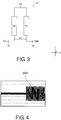
- FIG. 3 is an explanatory view showing a structure of the MR sensor 10 shown in FIG. 1 .
- the MR sensor 10 is magnetoresistive effect element including a first resistor R1 (hereinafter, referred to as a "resistor R1”) and a second resistor R2 (hereinafter, referred to as a “resistor R2”) connected in series.
- Each of the resistors R1 and R2 is formed of, for example, a thin film of a nickel-iron alloy.
- the resistors R1 and R2 are formed by being folded multiple times in the "Y" direction (a short widthwise direction of the card 2).
- the resistors R1 and R2 are formed by being folded twice in the "Y” direction.
- each of the resistors R1 and R2 is formed in a straight shape parallel to the "Y” direction.
- Each of the resistors R1 and R2 may be formed of any material in addition to a nickel-iron alloy.
- the resistor R2 is connected to a power supply Vcc. Specifically, one end of the resistor R2, which is not connected to the resistor R1, is connected to a connection terminal T1 to the power supply Vcc, and the connection terminal T1 is connected to the power supply Vcc.
- the resistor R1 is grounded. Specifically, one end of the resistor R1, which is not connected to the resistor R2, is connected to a ground terminal T2, and the ground terminal T2 is grounded. Further, the MR sensor 10 outputs a potential at a midpoint C1 between the resistor R1 and the resistor R2 connected in series (a node between the resistor R1 and the resistor R2).
- a resistance value of the resistor R1 and a resistance value of the resistor R2 are equal to each other.
- a length in the "Y” direction of the resistor R1 and a length in the "Y” direction of the resistor R2 are equal to each other. Further, this length is narrower than a width in the "Y” direction of the magnetic data recorded in the magnetic stripe 2a. This length is, for example, 2 mm.
- a width in the "X" direction of the resistor R1 and a width in the "X” direction of the resistor part R2 are equal to each other. This width is, for example, 60 ⁇ m.
- a thickness of the resistor R1 and a thickness of the resistor R2 are equal to each other. This thickness is, for example, 45 nm.
- the resistor R1 and the resistor R2 are located at the same position in the "Y” direction. Specifically, the resistor R1 and the resistor R2 are located at a position where the magnetic stripe 2a is passed in the "Y” direction. Further, the resistor R1 and the resistor R2 are disposed to be separated from each other by a distance D1 in the "X" direction.
- the distance D1 is less than a maximum bit interval of the magnetic data recorded in the magnetic stripe 2a. In other words, the distance D1 is less than a bit interval of magnetic data in a case that "0" data are recorded in the magnetic stripe 2a.
- the distance D1 corresponds to a half of a bit interval of magnetic data in the case that the "0" data are recorded in the magnetic stripe 2a.
- the distance D1 is identical to a bit interval of magnetic data in a case that "1" data are recorded in the magnetic stripe 2a.
- the distance D1 is a distance between a portion closest to the resistor R2 of the resistor R1 and a portion closest to the resistor R1 of the resistor R2.
- the resistor R1 and the resistor R2 are disposed to be separated from each other by the distance D1 in the "X" direction, and the distance D1 is a half of a bit interval of magnetic data in a case that "0" data are recorded in the magnetic stripe 2a.
- the distance in the "X" direction between the resistor R1 and the resistor R2 is very short. In this embodiment, therefore, it is possible to narrow a difference between an amount of change in resistance of the resistor R1 and an amount of change in resistance of the resistor R2, the difference being caused owing to a disturbing magnetic field generated by the disturbing magnetic field generating means 11.
- the distance D1 in the "X" direction between the resistor R1 and the resistor R2 is the half of the bit interval of the magnetic data in the case that the "0" data are recorded in the magnetic stripe 2a. It is therefore possible to widen a difference between an amount of change in resistance of the resistor R1 and an amount of change in resistance of the resistor R2, the difference being caused owing to the "0" data recorded in the magnetic stripe 2a.
- the resistance value of the resistor R1 and the resistance value of the resistor R2 are equal to each other, and the MR sensor 10 outputs the potential at the midpoint C1 between the resistor R1 and the resistor R2.
- the disturbing magnetic field generating means 11 when the card insertion detection mechanism (not shown) detects that the card 2 has been inserted into the card insertion port 3, the disturbing magnetic field generating means 11 generates a disturbing magnetic field, and electric power is supplied to the MR sensor 10.
- an output signal SG1 from the MR sensor 10 varies as shown in FIG. 4 .
- the amplitude of the output signal SG1 is lesser before a magnetic data recording region of the magnetic stripe 2a reaches the MR sensor 10 (in other words, before the preamble of the magnetic stripe 2a reaches the MR sensor 10).
- the amplitude of the output signal SG1 becomes greater.
- the MR sensor 10 can appropriately detect whether magnetic data are recorded in the magnetic stripe 2a of the card 2 inserted through the card insertion port 3.
Description
- At least an embodiment of the present invention relates to a card reader structured to perform reading of magnetic data recorded in a card and recording of magnetic data to the card.
- Conventionally, a card reader has been widely utilized, which performs reading of magnetic data recorded in a card and recording of magnetic data to the card. In an industry such as a financial institution where a card reader is utilized, illegal acquisition of magnetic data of a card by a fraudulent person who attaches a magnetic head to a card insertion part of a card reader, in other words, so-called skimming has conventionally become a large issue. In order to cope with the issue, a card reader has been proposed, which generates a disturbing magnetic field for preventing reading of magnetic data using a magnetic head for skimming (hereinafter, referred to as a "skimming magnetic head") (see, for example, Patent Literature 1).
- A card reader described in Patent Literature 1 includes: a disturbing magnetic field generator that generates a disturbing magnetic field; a conveying roller that conveys a card inserted through a card insertion port; and a motor that drives the conveying roller. The card reader also includes a magnetic head (pre-head) that detects whether magnetic data are recorded in a magnetic stripe of the card inserted through the card insertion port. In the card reader, when the pre-head detects that the magnetic data are recorded in the magnetic stripe of the card inserted through the card insertion port, the motor is activated to drive the conveying roller. The card is thus taken into the card reader. Also in the card reader, after the activation of the motor, the disturbing magnetic field generator generates a disturbing magnetic field during a period of time in which a rear end side of the card is protruded from the card insertion port.
- Patent Literature 1: Japanese Patent No.
3936496 - In the card reader described in Patent Literature 1, for the purpose of surely preventing skimming using a skimming magnetic head, preferably, the disturbing magnetic field generator generates a disturbing magnetic field before the magnetic stripe of the card inserted through the card insertion port reaches the pre-head and, further, the disturbing magnetic field generator generates a disturbing magnetic field for a predetermined period of time after the magnetic stripe has reached the pre-head. In other words, in the card reader described in Patent Literature 1, for the purpose of surely preventing skimming using a skimming magnetic head, preferably, a disturbing magnetic field is also generated at the time when the pre-head reads magnetic data.
- According to research of the present inventors, however, they have found that, in the card reader described in Patent Literature 1, in a case that a disturbing magnetic field is generated at the time when the pre-head reads magnetic data, an output signal from the pre-head varies owing to the disturbing magnetic field, which makes it difficult for the pre-head to appropriately detect whether magnetic data are recorded in a magnetic stripe. In other words, according to the examinations of the present inventors, they have found that, in the card reader described in Patent Literature 1, it is difficult for the pre-head to appropriately detect whether magnetic data are recorded in a magnetic stripe of a card inserted through the card insertion port, in a state in which a disturbing magnetic field is generated.
- In view of the problem described above, at least an embodiment of the present invention provides a card reader capable of appropriately detecting whether magnetic data are recorded in a magnetic stripe of a card inserted through a card insertion port, even in a state in which a disturbing magnetic field is generated.
- To achieve the above, at least an embodiment of the present invention provides a card reader according to claim 1. Preferred embodiments are subject of the dependent claims.
- In the card reader according to at least an embodiment of the present invention, the MR sensor for detecting whether magnetic data are recorded in a magnetic stripe includes the first resistor and the second resistor. In at least an embodiment of the present invention, further, the first resistor and the second resistor are disposed to be separated by the distance which is less than the bit interval of the magnetic data in the case that the "0" data are recorded in the magnetic stripe, from each other in the moving direction of the card, the moving direction being coincided with the arranging direction of the magnetic data. In other words, the distance between the first resistor and the second resistor is very short in the moving direction of the card. In at least an embodiment of the present invention, therefore, it is possible to narrow a difference between an amount of change in resistance of the first resistor and an amount of change in resistance of the second resistor, the difference being caused owing to a disturbing magnetic field generated by the disturbing magnetic field generating means. In at least an embodiment of the present invention, further, the first resistor and the second resistor are disposed to be separated by the distance which is less than the bit interval of the magnetic data in the case that the "0" data are recorded in the magnetic stripe, from each other in the moving direction of the card, the moving direction being coincided with the arranging direction of the magnetic data. It is therefore possible to widen a difference between an amount of change in resistance of the first resistor and an amount of change in resistance of the second resistor, the difference being caused owing to the magnetic data recorded in the magnetic stripe. In at least an embodiment of the present invention, accordingly, even in a state in which a disturbing magnetic field is generated, it is possible to appropriately detect whether magnetic data are recorded in a magnetic stripe of a card inserted through the card insertion port, based on a difference between an amount of change in resistance of the first resistor and an amount of change in resistance of the second resistor.
- In at least an embodiment of the present invention, preferably, the first resistor and the second resistor are disposed to be separated by a distance which is a half of the bit interval of the magnetic data in the case that the "0" data are recorded in the magnetic stripe, from each other in the moving direction of the card. The international standard or JIS standard specifies that "0" data are recorded in a preamble on a tip end side of a magnetic stripe. With this structure, in a case that magnetic data are recorded in a magnetic stripe of a card specified in the international standard or JIS standard, it is possible to further widen a difference between an amount of change in resistance of the first resistor and an amount of change in resistance of the second resistor, the difference being caused owing to the magnetic data. It is accordingly possible to more appropriately detect whether magnetic data are recorded in a magnetic stripe, based on a difference between an amount of change in resistance of the first resistor and an amount of change in resistance of the second resistor.
- In at least an embodiment of the present invention, preferably, the first resistor and the second resistor are connected in series, one of the first resistor and the second resistor is connected to a power supply, the other one of the first resistor and the second resistor is grounded, and the MR sensor outputs a potential at a midpoint between the first resistor and the second resistor. With this structure, the MR sensor outputs the difference between the amount of change in resistance of the first resistor and the amount of change in resistance of the second resistor as it is. Therefore, the output signal from the MR sensor can be processed with ease as compared with, for example, a case that the first resistor and the second resistor are connected in parallel.
- In at least an embodiment of the present invention, preferably, the MR sensor includes multiple sets of first resistors and multiple sets of second resistors, and the MR sensor detects whether magnetic data are recorded, for each track to be recorded in the magnetic stripe. With this structure, it is possible to more appropriately detect whether magnetic data of multiple tracks are recorded in a magnetic stripe.
- As described above, a card reader according to at least an embodiment of the present invention is capable of appropriately detecting whether magnetic data are recorded in a magnetic stripe of a card inserted through a card insertion port, even in a state in which a disturbing magnetic field is generated.
-
-
FIG. 1 is a schematic view showing a card reader in accordance with an embodiment of the present invention. -
FIG. 2 is a view showing a rear face of a card shown inFIG. 1 . -
FIG. 3 is an explanatory view showing a structure of an MR sensor shown inFIG. 1 . -
FIG. 4 is a view showing an exemplary output signal from the MR sensor shown inFIG. 3 . - Embodiments of the present invention will be described below with reference to the accompanying drawings.
-
FIG. 1 is a schematic view showing a card reader 1 in accordance with an embodiment of the present invention.FIG. 2 is a view showing a rear face of acard 2 shown inFIG. 1 . - The card reader 1 in this embodiment is a device for performing reading of magnetic data recorded in the
card 2 and recording of magnetic data to thecard 2 and is mounted for use on a predetermined host apparatus such as an automated teller machine (ATM). The card reader 1 includes acard insertion part 4 formed with acard insertion port 3 into which thecard 2 is inserted, and amain body part 5. An inside of the card reader 1 is formed with acard passage 6 where thecard 2 inserted through thecard insertion port 3 is passed. - In this embodiment, the
card 2 inserted through thecard insertion port 3 moves in an "X" direction shown inFIG. 1 . In other words, the "X" direction is a moving direction of thecard 2. Further, a "Z" direction inFIG. 1 perpendicular to the "X" direction is a thickness direction of thecard 2 taken into the card reader 1, and a "Y" direction inFIG. 1 perpendicular to the "X" direction and the "Z" direction is a width direction of thecard 2 taken into the card reader 1. - The
card 2 is a substantially rectangular-shaped card made of vinyl chloride whose thickness is about 0.7-0.8 mm. A rear face of thecard 2 is formed with amagnetic stripe 2a in which magnetic data are recorded. Themagnetic stripe 2a is formed along a longitudinal direction of thecard 2 formed in a substantially rectangular shape. The magnetic data recorded in themagnetic stripe 2a are arranged in a longitudinal direction of themagnetic stripe 2a (in other words, the longitudinal direction of the card 2). Thecard 2 in this embodiment is a card which is specified in the international standard or JIS standard, and "0" data are recorded on a preamble on a tip end side of themagnetic stripe 2a. - The
card 2 is inserted into the card reader 1 and moves inside the card reader 1 in a state in which its rear face is directed downward and its longitudinal direction is substantially coincided with the "X" direction (the moving direction of the card 2). In other words, the magnetic data recorded in themagnetic stripe 2a are arranged in the moving direction of thecard 2. An IC chip and a communication antenna may be incorporated into thecard 2. Further, thecard 2 may be a PET (polyethylene terephthalate) card whose thickness is about 0.18-0.36 mm and may be a paper card having a predetermined thickness. - The card reader 1 also includes a
magnetic head 7 that performs reading of magnetic data recorded in themagnetic stripe 2a of thecard 2 and recording of magnetic data to themagnetic stripe 2a, adrive roller 8 and apad roller 9 that convey thecard 2 along thecard passage 6, a magnetoresistive (MR)sensor 10 that detects whether magnetic data are recorded in themagnetic stripe 2a, and a disturbing magnetic field generating means 11 that generates a magnetic field (disturbing magnetic field) for preventing illegal reading of magnetic data recorded in themagnetic stripe 2a. - The
magnetic head 7, thedrive roller 8, and thepad roller 9 are disposed in themain body part 5. TheMR sensor 10 and the disturbing magnetic field generating means 11 are disposed in thecard insertion part 4. Themagnetic head 7 is disposed to face thecard passage 6 from below. Further, themagnetic head 7 is located at a position where themagnetic stripe 2a is passed in the "Y" direction. Thedrive roller 8 and thepad roller 9 are disposed to face each other in an upper and lower direction. Thepad roller 9 is urged toward thedrive roller 8. TheMR sensor 10 is disposed to face thecard passage 6 from below. A specific structure of theMR sensor 10 will be described later. - The disturbing magnetic field generating means 11 includes a core that is formed of a magnetic material, and an excitation coil that is wound around the core. For example, the core and the coil are disposed above the
card passage 6. The coil is connected to an alternating-current power supply circuit that feeds electric current to the coil. When electric current is fed to the coil, a disturbing magnetic field is generated toward a front side of the card reader 1 and toward the position where themagnetic stripe 2a is passed. The core and the coil may be disposed below thecard passage 6. - In the card reader 1, when a card insertion detection mechanism (not shown) detects that the
card 2 has been inserted into thecard insertion port 3, the disturbing magnetic field generating means 11 generates a disturbing magnetic field, and electric power is supplied to theMR sensor 10. -
FIG. 3 is an explanatory view showing a structure of theMR sensor 10 shown inFIG. 1 . - As shown in
FIG. 3 , theMR sensor 10 is magnetoresistive effect element including a first resistor R1 (hereinafter, referred to as a "resistor R1") and a second resistor R2 (hereinafter, referred to as a "resistor R2") connected in series. Each of the resistors R1 and R2 is formed of, for example, a thin film of a nickel-iron alloy. The resistors R1 and R2 are formed by being folded multiple times in the "Y" direction (a short widthwise direction of the card 2). For example, the resistors R1 and R2 are formed by being folded twice in the "Y" direction. Alternatively, each of the resistors R1 and R2 is formed in a straight shape parallel to the "Y" direction. Each of the resistors R1 and R2 may be formed of any material in addition to a nickel-iron alloy. - The resistor R2 is connected to a power supply Vcc. Specifically, one end of the resistor R2, which is not connected to the resistor R1, is connected to a connection terminal T1 to the power supply Vcc, and the connection terminal T1 is connected to the power supply Vcc. The resistor R1 is grounded. Specifically, one end of the resistor R1, which is not connected to the resistor R2, is connected to a ground terminal T2, and the ground terminal T2 is grounded. Further, the
MR sensor 10 outputs a potential at a midpoint C1 between the resistor R1 and the resistor R2 connected in series (a node between the resistor R1 and the resistor R2). - A resistance value of the resistor R1 and a resistance value of the resistor R2 are equal to each other. In this embodiment, a length in the "Y" direction of the resistor R1 and a length in the "Y" direction of the resistor R2 are equal to each other. Further, this length is narrower than a width in the "Y" direction of the magnetic data recorded in the
magnetic stripe 2a. This length is, for example, 2 mm. Further, a width in the "X" direction of the resistor R1 and a width in the "X" direction of the resistor part R2 are equal to each other. This width is, for example, 60 µm. Further, a thickness of the resistor R1 and a thickness of the resistor R2 are equal to each other. This thickness is, for example, 45 nm. - The resistor R1 and the resistor R2 are located at the same position in the "Y" direction. Specifically, the resistor R1 and the resistor R2 are located at a position where the
magnetic stripe 2a is passed in the "Y" direction. Further, the resistor R1 and the resistor R2 are disposed to be separated from each other by a distance D1 in the "X" direction. The distance D1 is less than a maximum bit interval of the magnetic data recorded in themagnetic stripe 2a. In other words, the distance D1 is less than a bit interval of magnetic data in a case that "0" data are recorded in themagnetic stripe 2a. - In this embodiment, the distance D1 corresponds to a half of a bit interval of magnetic data in the case that the "0" data are recorded in the
magnetic stripe 2a. In other words, the distance D1 is identical to a bit interval of magnetic data in a case that "1" data are recorded in themagnetic stripe 2a. For example, when a recording density of magnetic data recorded in themagnetic stripe 2a is 75 bpi, the distance D1 is 0.17 mm (= 25.4/(75 × 2)). Further, when a recording density of magnetic data recorded in themagnetic stripe 2a is 210 bpi, the distance D1 is 0.18 mm (= 25.4 × 3/(210 × 2)). In the case that the resistors R1 and R2 are formed by being folded multiple times in the "Y" direction, the distance D1 is a distance between a portion closest to the resistor R2 of the resistor R1 and a portion closest to the resistor R1 of the resistor R2. - As described above, in this embodiment, the resistor R1 and the resistor R2 are disposed to be separated from each other by the distance D1 in the "X" direction, and the distance D1 is a half of a bit interval of magnetic data in a case that "0" data are recorded in the
magnetic stripe 2a. In other words, in this embodiment, the distance in the "X" direction between the resistor R1 and the resistor R2 is very short. In this embodiment, therefore, it is possible to narrow a difference between an amount of change in resistance of the resistor R1 and an amount of change in resistance of the resistor R2, the difference being caused owing to a disturbing magnetic field generated by the disturbing magnetic field generating means 11. Also in this embodiment, the distance D1 in the "X" direction between the resistor R1 and the resistor R2 is the half of the bit interval of the magnetic data in the case that the "0" data are recorded in themagnetic stripe 2a. It is therefore possible to widen a difference between an amount of change in resistance of the resistor R1 and an amount of change in resistance of the resistor R2, the difference being caused owing to the "0" data recorded in themagnetic stripe 2a. - Also in this embodiment, the resistance value of the resistor R1 and the resistance value of the resistor R2 are equal to each other, and the
MR sensor 10 outputs the potential at the midpoint C1 between the resistor R1 and the resistor R2. Also in this embodiment, when the card insertion detection mechanism (not shown) detects that thecard 2 has been inserted into thecard insertion port 3, the disturbing magnetic field generating means 11 generates a disturbing magnetic field, and electric power is supplied to theMR sensor 10. In this embodiment, therefore, in a case that magnetic data are recorded in themagnetic stripe 2a of thecard 2 inserted into thecard insertion port 3, when thecard 2 moves toward the rear side of the card reader 1, an output signal SG1 from theMR sensor 10 varies as shown inFIG. 4 . - As shown in
FIG. 4 , the amplitude of the output signal SG1 is lesser before a magnetic data recording region of themagnetic stripe 2a reaches the MR sensor 10 (in other words, before the preamble of themagnetic stripe 2a reaches the MR sensor 10). When the preamble of themagnetic stripe 2a reaches theMR sensor 10, the amplitude of the output signal SG1 becomes greater. In this embodiment, accordingly, even in the state in which a disturbing magnetic field is generated, theMR sensor 10 can appropriately detect whether magnetic data are recorded in themagnetic stripe 2a of thecard 2 inserted through thecard insertion port 3. - Described above is an example of a preferred embodiment according to the present invention. However, the present invention is not limited to the above embodiment and various variations and modifications may be made without changing the concept of the present invention.
-
- 1: card reader
- 2: card
- 2a: magnetic stripe
- 3: card insertion port
- 10: MR sensor
- 11: disturbing magnetic field generating means
- C1: midpoint
- R1: resistor (first resistor)
- R2: resistor (second resistor)
- X: moving direction of card
Claims (3)
- A card reader (1) comprising:a card insertion port (3) into which a card (2) having a magnetic stripe (2a) is inserted;a magnetoresistive (MR) sensor (10) configured to detect whether magnetic data are recorded in the magnetic stripe (2a) arranged in a moving direction (X) of the card (2) inserted through the card insertion port (3); anda disturbing magnetic field generating means (11) that generates a disturbing magnetic field for disturbing illegal reading of the magnetic data recorded in the magnetic stripe (2a),characterized in that the MR sensor includes at least a first resistor (R1) and at least a second resistor (R2) that are disposed to be separated by a distance (D1) which is a half of a bit interval of magnetic data in a case that "0" data are recorded in the magnetic stripe (2a), from each other in the moving direction (X) of the card (2), wherein the distance (D1) is 0.17 mm or 0.18 mm.
- The card reader (1) according to claim 1, wherein
the first resistor (R1) and the second resistor (R2) are connected in series,
one of the first resistor (R1) and the second resistor (R2) is connected to a power supply,
the other one of the first resistor (R1) and the second resistor (R2) is grounded, and
the MR sensor (10) outputs a potential at a midpoint (C1) between the first resistor (R1) and the second resistor (R2). - The card reader (1) according to any one of claims 1 to 2, wherein
the MR sensor (10) includes multiple sets of the first resistors (R1) and multiple sets of the second resistors (R2), and
the MR sensor (10) detects whether magnetic data are recorded, for each track to be recorded in the magnetic stripe (2a).
Applications Claiming Priority (2)
| Application Number | Priority Date | Filing Date | Title |
|---|---|---|---|
| JP2015067983A JP2016189055A (en) | 2015-03-30 | 2015-03-30 | Card reader |
| PCT/JP2016/060130 WO2016158952A1 (en) | 2015-03-30 | 2016-03-29 | Card reader |
Publications (3)
| Publication Number | Publication Date |
|---|---|
| EP3279828A1 EP3279828A1 (en) | 2018-02-07 |
| EP3279828A4 EP3279828A4 (en) | 2018-11-07 |
| EP3279828B1 true EP3279828B1 (en) | 2019-10-30 |
Family
ID=57005951
Family Applications (1)
| Application Number | Title | Priority Date | Filing Date |
|---|---|---|---|
| EP16772833.6A Active EP3279828B1 (en) | 2015-03-30 | 2016-03-29 | Card reader |
Country Status (5)
| Country | Link |
|---|---|
| US (1) | US10055615B2 (en) |
| EP (1) | EP3279828B1 (en) |
| JP (1) | JP2016189055A (en) |
| CN (1) | CN107430674B (en) |
| WO (1) | WO2016158952A1 (en) |
Families Citing this family (4)
| Publication number | Priority date | Publication date | Assignee | Title |
|---|---|---|---|---|
| JP7085814B2 (en) * | 2017-08-31 | 2022-06-17 | 日本電産サンキョー株式会社 | Card reader |
| US10496914B2 (en) * | 2017-10-31 | 2019-12-03 | University Of Florida Research Foundation, Incorporated | Payment card overlay skimmer detection |
| JP2020113357A (en) * | 2019-01-17 | 2020-07-27 | 日本電産サンキョー株式会社 | Magnetic recording medium processor and control method |
| CN112085905B (en) * | 2019-06-14 | 2022-03-01 | 中电金融设备系统(深圳)有限公司 | Magnetic stripe card reader, magnetic stripe data processing device and magnetic stripe data processing method |
Family Cites Families (16)
| Publication number | Priority date | Publication date | Assignee | Title |
|---|---|---|---|---|
| JPS58129585A (en) | 1982-01-27 | 1983-08-02 | Denki Onkyo Co Ltd | Pattern recognizing device using magnetoresistance element |
| US5266786A (en) | 1991-10-01 | 1993-11-30 | Ncr Corporation | Magnetoresistive head for reading magnetic ink characters |
| JPH08145718A (en) * | 1994-11-17 | 1996-06-07 | Canon Electron Inc | Magneto-resistive sensor |
| JPH097119A (en) * | 1995-06-19 | 1997-01-10 | Oki Electric Ind Co Ltd | Magnetic head array and its production |
| US5650606A (en) | 1995-08-07 | 1997-07-22 | Magnetic Products International, Corp | Accurate read/write head for preventing credit card alteration and counterfeiting of debit cards |
| JP3936496B2 (en) * | 1999-08-31 | 2007-06-27 | 日本電産サンキョー株式会社 | Magnetic card transaction device |
| US20080290167A1 (en) * | 2007-05-24 | 2008-11-27 | Clay Von Mueller | Multi dimensional read head array |
| JP5728791B2 (en) * | 2009-03-05 | 2015-06-03 | 日本電産サンキョー株式会社 | Card reader |
| EP2657888B1 (en) * | 2010-12-22 | 2020-02-12 | Hitachi-Omron Terminal Solutions, Corp. | Apparatus for reading magnetic recording medium |
| JP5759807B2 (en) * | 2011-06-29 | 2015-08-05 | 日本電産サンキョー株式会社 | Card insertion part and card reader |
| EP2752823B1 (en) * | 2011-08-30 | 2019-08-28 | Hitachi-Omron Terminal Solutions, Corporation | Device for reading magnetic recording medium |
| EP2752825B1 (en) * | 2011-08-30 | 2017-03-22 | Hitachi-Omron Terminal Solutions, Corporation | Device for reading magnetic recording medium |
| WO2013118183A1 (en) * | 2012-02-09 | 2013-08-15 | 日立オムロンターミナルソリューションズ株式会社 | Magnetic card reader and magnetic card reading method |
| JP5648024B2 (en) * | 2012-07-10 | 2015-01-07 | 日本電産サンキョー株式会社 | Card reader |
| WO2014195991A1 (en) * | 2013-06-04 | 2014-12-11 | 日立オムロンターミナルソリューションズ株式会社 | Magnetic recording medium reader |
| DE102014119663A1 (en) * | 2014-12-29 | 2016-06-30 | Infineon Technologies Ag | smart card |
-
2015
- 2015-03-30 JP JP2015067983A patent/JP2016189055A/en active Pending
-
2016
- 2016-03-29 US US15/563,091 patent/US10055615B2/en active Active
- 2016-03-29 WO PCT/JP2016/060130 patent/WO2016158952A1/en active Application Filing
- 2016-03-29 CN CN201680019128.XA patent/CN107430674B/en active Active
- 2016-03-29 EP EP16772833.6A patent/EP3279828B1/en active Active
Non-Patent Citations (1)
| Title |
|---|
| None * |
Also Published As
| Publication number | Publication date |
|---|---|
| US10055615B2 (en) | 2018-08-21 |
| CN107430674A (en) | 2017-12-01 |
| EP3279828A4 (en) | 2018-11-07 |
| JP2016189055A (en) | 2016-11-04 |
| EP3279828A1 (en) | 2018-02-07 |
| WO2016158952A1 (en) | 2016-10-06 |
| CN107430674B (en) | 2020-03-27 |
| US20180075263A1 (en) | 2018-03-15 |
Similar Documents
| Publication | Publication Date | Title |
|---|---|---|
| US8985450B2 (en) | Card insertion part and card reader | |
| EP3279828B1 (en) | Card reader | |
| US8824073B2 (en) | Card reader and control method of card reader | |
| CN106022182B (en) | The control method of card reader and card reader | |
| US9626820B2 (en) | Card reader | |
| EP3168773A1 (en) | Card reader | |
| US20170185811A1 (en) | Card reader and control method for card reader | |
| US9218548B2 (en) | Card reader and control method therefor | |
| US10043044B2 (en) | Card reader | |
| EP3190588B1 (en) | Mr sensor and card reader | |
| JP7307167B2 (en) | A reader for reading information stored on a magnetic stripe and a method for decoding the read information | |
| US10083327B2 (en) | Card reader and control method therefor | |
| JP2019061398A (en) | Magnetic sensor unit and card reader | |
| JPH11238203A (en) | Magnetic recording device |
Legal Events
| Date | Code | Title | Description |
|---|---|---|---|
| STAA | Information on the status of an ep patent application or granted ep patent |
Free format text: STATUS: THE INTERNATIONAL PUBLICATION HAS BEEN MADE |
|
| PUAI | Public reference made under article 153(3) epc to a published international application that has entered the european phase |
Free format text: ORIGINAL CODE: 0009012 |
|
| STAA | Information on the status of an ep patent application or granted ep patent |
Free format text: STATUS: REQUEST FOR EXAMINATION WAS MADE |
|
| 17P | Request for examination filed |
Effective date: 20171026 |
|
| AK | Designated contracting states |
Kind code of ref document: A1 Designated state(s): AL AT BE BG CH CY CZ DE DK EE ES FI FR GB GR HR HU IE IS IT LI LT LU LV MC MK MT NL NO PL PT RO RS SE SI SK SM TR |
|
| AX | Request for extension of the european patent |
Extension state: BA ME |
|
| DAV | Request for validation of the european patent (deleted) | ||
| DAX | Request for extension of the european patent (deleted) | ||
| A4 | Supplementary search report drawn up and despatched |
Effective date: 20181009 |
|
| RIC1 | Information provided on ipc code assigned before grant |
Ipc: G06K 7/10 20060101ALI20181002BHEP Ipc: G06K 19/073 20060101ALI20181002BHEP Ipc: G06K 7/08 20060101AFI20181002BHEP |
|
| GRAP | Despatch of communication of intention to grant a patent |
Free format text: ORIGINAL CODE: EPIDOSNIGR1 |
|
| STAA | Information on the status of an ep patent application or granted ep patent |
Free format text: STATUS: GRANT OF PATENT IS INTENDED |
|
| INTG | Intention to grant announced |
Effective date: 20190603 |
|
| GRAS | Grant fee paid |
Free format text: ORIGINAL CODE: EPIDOSNIGR3 |
|
| GRAA | (expected) grant |
Free format text: ORIGINAL CODE: 0009210 |
|
| STAA | Information on the status of an ep patent application or granted ep patent |
Free format text: STATUS: THE PATENT HAS BEEN GRANTED |
|
| AK | Designated contracting states |
Kind code of ref document: B1 Designated state(s): AL AT BE BG CH CY CZ DE DK EE ES FI FR GB GR HR HU IE IS IT LI LT LU LV MC MK MT NL NO PL PT RO RS SE SI SK SM TR |
|
| REG | Reference to a national code |
Ref country code: GB Ref legal event code: FG4D |
|
| REG | Reference to a national code |
Ref country code: CH Ref legal event code: EP |
|
| REG | Reference to a national code |
Ref country code: AT Ref legal event code: REF Ref document number: 1196939 Country of ref document: AT Kind code of ref document: T Effective date: 20191115 |
|
| REG | Reference to a national code |
Ref country code: DE Ref legal event code: R096 Ref document number: 602016023398 Country of ref document: DE |
|
| REG | Reference to a national code |
Ref country code: IE Ref legal event code: FG4D |
|
| REG | Reference to a national code |
Ref country code: LT Ref legal event code: MG4D |
|
| PG25 | Lapsed in a contracting state [announced via postgrant information from national office to epo] |
Ref country code: NL Free format text: LAPSE BECAUSE OF FAILURE TO SUBMIT A TRANSLATION OF THE DESCRIPTION OR TO PAY THE FEE WITHIN THE PRESCRIBED TIME-LIMIT Effective date: 20191030 Ref country code: SE Free format text: LAPSE BECAUSE OF FAILURE TO SUBMIT A TRANSLATION OF THE DESCRIPTION OR TO PAY THE FEE WITHIN THE PRESCRIBED TIME-LIMIT Effective date: 20191030 Ref country code: LV Free format text: LAPSE BECAUSE OF FAILURE TO SUBMIT A TRANSLATION OF THE DESCRIPTION OR TO PAY THE FEE WITHIN THE PRESCRIBED TIME-LIMIT Effective date: 20191030 Ref country code: PT Free format text: LAPSE BECAUSE OF FAILURE TO SUBMIT A TRANSLATION OF THE DESCRIPTION OR TO PAY THE FEE WITHIN THE PRESCRIBED TIME-LIMIT Effective date: 20200302 Ref country code: BG Free format text: LAPSE BECAUSE OF FAILURE TO SUBMIT A TRANSLATION OF THE DESCRIPTION OR TO PAY THE FEE WITHIN THE PRESCRIBED TIME-LIMIT Effective date: 20200130 Ref country code: FI Free format text: LAPSE BECAUSE OF FAILURE TO SUBMIT A TRANSLATION OF THE DESCRIPTION OR TO PAY THE FEE WITHIN THE PRESCRIBED TIME-LIMIT Effective date: 20191030 Ref country code: GR Free format text: LAPSE BECAUSE OF FAILURE TO SUBMIT A TRANSLATION OF THE DESCRIPTION OR TO PAY THE FEE WITHIN THE PRESCRIBED TIME-LIMIT Effective date: 20200131 Ref country code: LT Free format text: LAPSE BECAUSE OF FAILURE TO SUBMIT A TRANSLATION OF THE DESCRIPTION OR TO PAY THE FEE WITHIN THE PRESCRIBED TIME-LIMIT Effective date: 20191030 Ref country code: NO Free format text: LAPSE BECAUSE OF FAILURE TO SUBMIT A TRANSLATION OF THE DESCRIPTION OR TO PAY THE FEE WITHIN THE PRESCRIBED TIME-LIMIT Effective date: 20200130 Ref country code: PL Free format text: LAPSE BECAUSE OF FAILURE TO SUBMIT A TRANSLATION OF THE DESCRIPTION OR TO PAY THE FEE WITHIN THE PRESCRIBED TIME-LIMIT Effective date: 20191030 |
|
| PGFP | Annual fee paid to national office [announced via postgrant information from national office to epo] |
Ref country code: GB Payment date: 20200318 Year of fee payment: 5 |
|
| REG | Reference to a national code |
Ref country code: NL Ref legal event code: MP Effective date: 20191030 |
|
| PG25 | Lapsed in a contracting state [announced via postgrant information from national office to epo] |
Ref country code: RS Free format text: LAPSE BECAUSE OF FAILURE TO SUBMIT A TRANSLATION OF THE DESCRIPTION OR TO PAY THE FEE WITHIN THE PRESCRIBED TIME-LIMIT Effective date: 20191030 Ref country code: HR Free format text: LAPSE BECAUSE OF FAILURE TO SUBMIT A TRANSLATION OF THE DESCRIPTION OR TO PAY THE FEE WITHIN THE PRESCRIBED TIME-LIMIT Effective date: 20191030 Ref country code: IS Free format text: LAPSE BECAUSE OF FAILURE TO SUBMIT A TRANSLATION OF THE DESCRIPTION OR TO PAY THE FEE WITHIN THE PRESCRIBED TIME-LIMIT Effective date: 20200229 |
|
| PG25 | Lapsed in a contracting state [announced via postgrant information from national office to epo] |
Ref country code: AL Free format text: LAPSE BECAUSE OF FAILURE TO SUBMIT A TRANSLATION OF THE DESCRIPTION OR TO PAY THE FEE WITHIN THE PRESCRIBED TIME-LIMIT Effective date: 20191030 |
|
| PG25 | Lapsed in a contracting state [announced via postgrant information from national office to epo] |
Ref country code: RO Free format text: LAPSE BECAUSE OF FAILURE TO SUBMIT A TRANSLATION OF THE DESCRIPTION OR TO PAY THE FEE WITHIN THE PRESCRIBED TIME-LIMIT Effective date: 20191030 Ref country code: ES Free format text: LAPSE BECAUSE OF FAILURE TO SUBMIT A TRANSLATION OF THE DESCRIPTION OR TO PAY THE FEE WITHIN THE PRESCRIBED TIME-LIMIT Effective date: 20191030 Ref country code: CZ Free format text: LAPSE BECAUSE OF FAILURE TO SUBMIT A TRANSLATION OF THE DESCRIPTION OR TO PAY THE FEE WITHIN THE PRESCRIBED TIME-LIMIT Effective date: 20191030 Ref country code: DK Free format text: LAPSE BECAUSE OF FAILURE TO SUBMIT A TRANSLATION OF THE DESCRIPTION OR TO PAY THE FEE WITHIN THE PRESCRIBED TIME-LIMIT Effective date: 20191030 Ref country code: EE Free format text: LAPSE BECAUSE OF FAILURE TO SUBMIT A TRANSLATION OF THE DESCRIPTION OR TO PAY THE FEE WITHIN THE PRESCRIBED TIME-LIMIT Effective date: 20191030 |
|
| REG | Reference to a national code |
Ref country code: DE Ref legal event code: R097 Ref document number: 602016023398 Country of ref document: DE |
|
| REG | Reference to a national code |
Ref country code: AT Ref legal event code: MK05 Ref document number: 1196939 Country of ref document: AT Kind code of ref document: T Effective date: 20191030 |
|
| PG25 | Lapsed in a contracting state [announced via postgrant information from national office to epo] |
Ref country code: SK Free format text: LAPSE BECAUSE OF FAILURE TO SUBMIT A TRANSLATION OF THE DESCRIPTION OR TO PAY THE FEE WITHIN THE PRESCRIBED TIME-LIMIT Effective date: 20191030 Ref country code: IT Free format text: LAPSE BECAUSE OF FAILURE TO SUBMIT A TRANSLATION OF THE DESCRIPTION OR TO PAY THE FEE WITHIN THE PRESCRIBED TIME-LIMIT Effective date: 20191030 Ref country code: SM Free format text: LAPSE BECAUSE OF FAILURE TO SUBMIT A TRANSLATION OF THE DESCRIPTION OR TO PAY THE FEE WITHIN THE PRESCRIBED TIME-LIMIT Effective date: 20191030 |
|
| PLBE | No opposition filed within time limit |
Free format text: ORIGINAL CODE: 0009261 |
|
| STAA | Information on the status of an ep patent application or granted ep patent |
Free format text: STATUS: NO OPPOSITION FILED WITHIN TIME LIMIT |
|
| 26N | No opposition filed |
Effective date: 20200731 |
|
| PG25 | Lapsed in a contracting state [announced via postgrant information from national office to epo] |
Ref country code: MC Free format text: LAPSE BECAUSE OF FAILURE TO SUBMIT A TRANSLATION OF THE DESCRIPTION OR TO PAY THE FEE WITHIN THE PRESCRIBED TIME-LIMIT Effective date: 20191030 |
|
| REG | Reference to a national code |
Ref country code: CH Ref legal event code: PL |
|
| PG25 | Lapsed in a contracting state [announced via postgrant information from national office to epo] |
Ref country code: SI Free format text: LAPSE BECAUSE OF FAILURE TO SUBMIT A TRANSLATION OF THE DESCRIPTION OR TO PAY THE FEE WITHIN THE PRESCRIBED TIME-LIMIT Effective date: 20191030 Ref country code: AT Free format text: LAPSE BECAUSE OF FAILURE TO SUBMIT A TRANSLATION OF THE DESCRIPTION OR TO PAY THE FEE WITHIN THE PRESCRIBED TIME-LIMIT Effective date: 20191030 |
|
| REG | Reference to a national code |
Ref country code: BE Ref legal event code: MM Effective date: 20200331 |
|
| PG25 | Lapsed in a contracting state [announced via postgrant information from national office to epo] |
Ref country code: LU Free format text: LAPSE BECAUSE OF NON-PAYMENT OF DUE FEES Effective date: 20200329 |
|
| PG25 | Lapsed in a contracting state [announced via postgrant information from national office to epo] |
Ref country code: FR Free format text: LAPSE BECAUSE OF NON-PAYMENT OF DUE FEES Effective date: 20200331 Ref country code: CH Free format text: LAPSE BECAUSE OF NON-PAYMENT OF DUE FEES Effective date: 20200331 Ref country code: LI Free format text: LAPSE BECAUSE OF NON-PAYMENT OF DUE FEES Effective date: 20200331 Ref country code: IE Free format text: LAPSE BECAUSE OF NON-PAYMENT OF DUE FEES Effective date: 20200329 |
|
| PG25 | Lapsed in a contracting state [announced via postgrant information from national office to epo] |
Ref country code: BE Free format text: LAPSE BECAUSE OF NON-PAYMENT OF DUE FEES Effective date: 20200331 |
|
| GBPC | Gb: european patent ceased through non-payment of renewal fee |
Effective date: 20210329 |
|
| PG25 | Lapsed in a contracting state [announced via postgrant information from national office to epo] |
Ref country code: GB Free format text: LAPSE BECAUSE OF NON-PAYMENT OF DUE FEES Effective date: 20210329 |
|
| PG25 | Lapsed in a contracting state [announced via postgrant information from national office to epo] |
Ref country code: TR Free format text: LAPSE BECAUSE OF FAILURE TO SUBMIT A TRANSLATION OF THE DESCRIPTION OR TO PAY THE FEE WITHIN THE PRESCRIBED TIME-LIMIT Effective date: 20191030 Ref country code: MT Free format text: LAPSE BECAUSE OF FAILURE TO SUBMIT A TRANSLATION OF THE DESCRIPTION OR TO PAY THE FEE WITHIN THE PRESCRIBED TIME-LIMIT Effective date: 20191030 Ref country code: CY Free format text: LAPSE BECAUSE OF FAILURE TO SUBMIT A TRANSLATION OF THE DESCRIPTION OR TO PAY THE FEE WITHIN THE PRESCRIBED TIME-LIMIT Effective date: 20191030 |
|
| PG25 | Lapsed in a contracting state [announced via postgrant information from national office to epo] |
Ref country code: MK Free format text: LAPSE BECAUSE OF FAILURE TO SUBMIT A TRANSLATION OF THE DESCRIPTION OR TO PAY THE FEE WITHIN THE PRESCRIBED TIME-LIMIT Effective date: 20191030 |
|
| PGFP | Annual fee paid to national office [announced via postgrant information from national office to epo] |
Ref country code: DE Payment date: 20230320 Year of fee payment: 8 |