WO2016158643A1 - サーマルプリントヘッド、および、サーマルプリントヘッドの製造方法 - Google Patents
サーマルプリントヘッド、および、サーマルプリントヘッドの製造方法 Download PDFInfo
- Publication number
- WO2016158643A1 WO2016158643A1 PCT/JP2016/059312 JP2016059312W WO2016158643A1 WO 2016158643 A1 WO2016158643 A1 WO 2016158643A1 JP 2016059312 W JP2016059312 W JP 2016059312W WO 2016158643 A1 WO2016158643 A1 WO 2016158643A1
- Authority
- WO
- WIPO (PCT)
- Prior art keywords
- print head
- thermal print
- layer
- head according
- scanning direction
- Prior art date
- Legal status (The legal status is an assumption and is not a legal conclusion. Google has not performed a legal analysis and makes no representation as to the accuracy of the status listed.)
- Ceased
Links
Images











Classifications
-
- B—PERFORMING OPERATIONS; TRANSPORTING
- B41—PRINTING; LINING MACHINES; TYPEWRITERS; STAMPS
- B41J—TYPEWRITERS; SELECTIVE PRINTING MECHANISMS, i.e. MECHANISMS PRINTING OTHERWISE THAN FROM A FORME; CORRECTION OF TYPOGRAPHICAL ERRORS
- B41J2/00—Typewriters or selective printing mechanisms characterised by the printing or marking process for which they are designed
- B41J2/315—Typewriters or selective printing mechanisms characterised by the printing or marking process for which they are designed characterised by selective application of heat to a heat sensitive printing or impression-transfer material
- B41J2/32—Typewriters or selective printing mechanisms characterised by the printing or marking process for which they are designed characterised by selective application of heat to a heat sensitive printing or impression-transfer material using thermal heads
-
- B—PERFORMING OPERATIONS; TRANSPORTING
- B41—PRINTING; LINING MACHINES; TYPEWRITERS; STAMPS
- B41J—TYPEWRITERS; SELECTIVE PRINTING MECHANISMS, i.e. MECHANISMS PRINTING OTHERWISE THAN FROM A FORME; CORRECTION OF TYPOGRAPHICAL ERRORS
- B41J2/00—Typewriters or selective printing mechanisms characterised by the printing or marking process for which they are designed
- B41J2/315—Typewriters or selective printing mechanisms characterised by the printing or marking process for which they are designed characterised by selective application of heat to a heat sensitive printing or impression-transfer material
- B41J2/32—Typewriters or selective printing mechanisms characterised by the printing or marking process for which they are designed characterised by selective application of heat to a heat sensitive printing or impression-transfer material using thermal heads
- B41J2/335—Structure of thermal heads
Definitions
- the present invention relates to a thermal print head and a method for manufacturing the thermal print head.
- a conventionally known thermal print head includes a substrate, a glaze layer, a heating resistor, and an electrode.
- a thermal print head is disclosed in Patent Document 1, for example.
- the glaze layer is formed on the substrate.
- the glaze layer plays a role of storing heat generated by the heating resistor.
- the heating resistor is formed in the glaze layer.
- the electrode has two parts spaced apart from each other. A heating part is formed in the heating resistor so as to straddle these two parts.
- the thermal print head is built into the printer and is a basic module that determines the print quality of the printer. For this reason, the mounting accuracy of the thermal print head to the printer is important.
- the present invention has been conceived under the circumstances described above, and its main problem is to provide a thermal print head and a method for manufacturing a thermal print head that can improve the accuracy of attachment to a printer. And
- the thermal print head provided by the first aspect of the present invention includes a base material made of a semiconductor, a resistor layer that is supported by the base material and has a heat generating portion that generates heat when energized, and is formed on the base material.
- An electrode layer electrically connected to the resistor layer and an insulating layer are provided, and a position confirmation mark made of the same material as that of the resistor layer supported by the base material is formed.
- the electrode layer includes a first conductive portion and a second conductive portion that are separated from each other, and the heat generating portion is the first conductive portion in the thickness direction of the base material. And straddling the second conductive portion.
- the insulating layer has a portion interposed between the electrode layer and the heat generating portion.
- the insulating layer has a first interposed portion and a second interposed portion, and the first interposed portion is interposed between the first conductive portion and the heat generating portion.
- the second interposed portion is interposed between the second conductive portion and the heat generating portion.
- the insulating layer has an intermediate portion sandwiched between the first interposed portion and the second interposed portion in the thickness direction of the base material, and the intermediate portion Is connected to the first interposition part and the second interposition part.
- the first interposition part has a first opening
- the heat generating part has a first contact part that directly contacts a part of the first conductive part.
- the first contact portion is located at a position overlapping the first opening when viewed in the thickness direction of the base material.
- a part of the first conductive portion is formed in the first opening.
- a second opening is formed in the second interposition part, and the heat generating part has a second contact part in direct contact with a part of the second conductive part.
- the second contact portion is located at a position overlapping the second opening in the thickness direction of the base material.
- a part of the second conductive portion is formed in the second opening.
- the resistor layer has a first end surface facing a side opposite to a side where the second conductive portion is located, and the insulating layer is connected to the first interposed portion. And the part which covers the said 1st end surface is included.
- the resistor layer has a second end surface facing a side opposite to a side where the first conductive portion is located, and the insulating layer is connected to the second interposed portion. And the part which covers the said 2nd end surface is included.
- a heat storage layer interposed between the resistor layer and the position confirmation mark and the substrate is provided.
- the resistor layer and the position confirmation mark are in direct contact with the heat storage layer.
- the semiconductor device further includes a protective layer covering the resistor layer, the electrode layer, and the insulating layer, and the position confirmation mark is exposed from the protective layer.
- the protective layer is opaque.
- the protective layer is black.
- the protective layer is made of at least one of SiAlON, SiC, and CSiC.
- the position confirmation mark has a main scanning direction portion extending in the main scanning direction and a sub scanning direction portion extending in the sub scanning direction.
- the main scanning direction portion and the sub scanning direction portion intersect each other.
- the main scanning direction portion and the sub-scanning direction portion intersect each other at the center portion.
- a test electrode layer conducting to the position confirmation mark is provided.
- the test electrode layer is made of the same material as the electrode layer.
- the test electrode layer includes a wiring portion connected to the position confirmation mark and a test pad portion connected to the wiring portion.
- the wiring section is connected to both ends of the sub-scanning direction section in the sub-scanning direction.
- the sub-scanning direction portion and the main scanning direction portion are separated from each other.
- a wiring board, a plurality of wires, and a resin layer covering the wiring board, the plurality of wires, and the protective layer are further provided.
- a through window is formed in the protective layer, and the electrode layer includes a bonding portion exposed from the through window, and the bonding portion includes the plurality of wires. One of them is bonded.
- the resin layer is in direct contact with the protective layer.
- the semiconductor device further includes a drive IC for passing a current through the electrode layer, and the drive IC is mounted on the wiring board.
- the insulating layer is made of SiO2 or SiAlO2.
- the resistor layer is made of at least one of polysilicon, TaSiO2, and TiON.
- the electrode layer is made of at least one of Au, Ag, Cu, Cr, Al—Si, and Ti.
- the electrode layer includes a barrier metal layer in direct contact with the heat generating portion.
- the thermal printhead manufacturing method provided by the second aspect of the present invention is the thermal printhead manufacturing method provided by the first aspect of the present invention, wherein the resistor layer and the substrate are formed on the substrate.
- the step of forming the resistor layer is performed by CVD or sputtering.
- the resistor layer is made of at least one of polysilicon, TaSiO 2 , and TiON.
- the step of forming the electrode layer is performed by CVD or sputtering.
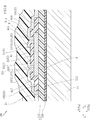
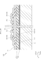
- FIG. 2 is a cross-sectional view taken along the line II-II in FIG.
- FIG. 2 is a partially enlarged plan view (partially omitted) of the thermal print head shown in FIG. 1.
- FIG. 4 is a partially enlarged plan view of a region IV in FIG. 3. It is a top view which abbreviate
- FIG. 4 is a partially enlarged sectional view taken along line VI-VI in FIG. 3.
- FIG. 2 is an enlarged plan view of a principal part (partially omitted in configuration) showing a specific example of the thermal print head shown in FIG. 1.
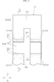
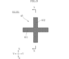
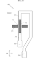
- FIG. 2 is an enlarged plan view of a main part showing a position confirmation mark of the thermal print head shown in FIG. 1.
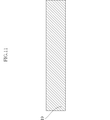
- FIG. 10 is a cross-sectional view of a main part taken along line XX in FIG. 9. It is sectional drawing which shows 1 process of the manufacturing process of the thermal print head shown in FIG.
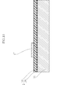
- FIG. 12 is a cross-sectional view showing a step subsequent to FIG. 11.
- FIG. 13 is a cross-sectional view showing a step subsequent to FIG. 12.
- FIG. 14 is a cross-sectional view showing a step subsequent to FIG. 13.
- FIG. 15 is a cross-sectional view showing a step subsequent to FIG. 14.
- FIG. 16 is a partially enlarged plan view when the step shown in FIG. 15 is performed.
- FIG. 16 is a cross-sectional view showing a step subsequent to FIG. 15.
- FIG. 18 is a cross-sectional view showing a step subsequent to FIG. 17. It is a partial enlarged plan view when the process shown in FIG. 18 is performed.
- FIG. 19 is a cross-sectional view showing a step subsequent to FIG. 18. It is a partial enlarged plan view when the process shown in FIG. 20 is performed.
- FIG. 21 is a cross-sectional view showing a step subsequent to FIG. 20. It is a partial enlarged plan view when the process shown in FIG. 22 is performed.
- FIG. 24 is a partially enlarged plan view showing one process following FIG. 23.
- FIG. 25 is a cross-sectional view showing a step subsequent to FIG. 24.
- FIG. 26 is a cross-sectional view showing a step subsequent to FIG. 25.
- (A)-(d) is an enlarged plan view of a main part showing a modification of the position confirmation mark. It is a principal part enlarged plan view which shows the thermal print head of 2nd Embodiment of this invention.
- FIG. 29 is an essential part enlarged cross-sectional view along the line XXIX-XXIX in FIG. 28. It is a principal part enlarged plan view which shows the thermal print head of 3rd Embodiment of this invention.
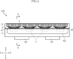
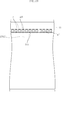
- FIG. 1 is a plan view of the thermal print head according to the first embodiment of the present invention.
- FIG. 2 is a sectional view taken along line II-II in FIG.
- the X direction is the sub-scanning direction
- the Y direction is the main scanning direction.
- the thermal print head 101 shown in these drawings includes a base material 11, a wiring board 12, a heat sink 13, a heat storage layer 2, an electrode layer 3, a resistor layer 4, a position confirmation mark 45, and an insulating layer. 5, a protective layer 6 (not shown in FIG. 1), a drive IC 7, a plurality of wires 81, a sealing resin 82, and a connector 83.
- the thermal print head 101 is incorporated in a printer that performs printing on the print medium 801. Examples of such a print medium 801 include thermal paper for creating a barcode sheet or a receipt.
- the heat sink 13 is made of a metal such as Al.
- a base material 11 and a wiring board 12 are attached to the heat sink 13.
- the substrate 11 has a plate shape.
- the base material 11 is made of a semiconductor material.
- the semiconductor material constituting the substrate 11 include Si, SiC, AlN, GaP, GaAs, InP, and GaN.
- Si is mentioned as a material of the base material 11 preferable for the configuration described below.
- the thickness of the substrate 11 is, for example, 0.625 to 0.720 mm.
- the base material 11 has a flat plate shape extending in the direction Y.
- the width of the base material 11 (the dimension in the direction X of the base material 11) is, for example, 3 to 20 mm.
- the dimension in the direction Y of the base material 11 is, for example, 10 to 300 mm.
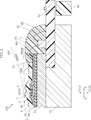
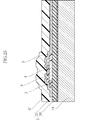
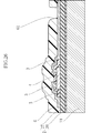
- FIG. 3 is a partially enlarged plan view (partially omitted) schematically showing the thermal print head 101 shown in FIG. 6 is a partially enlarged cross-sectional view taken along the line VI-VI in FIG.
- FIG. 7 is a partially enlarged plan view of the main part showing the shape of the components of the thermal print head 101 more faithfully.
- the protective layer 6 and the sealing resin 82 are omitted.
- the insulating layer 5, the protective layer 6, and the sealing resin 82 are omitted.
- the substrate 11 has a substrate surface 111.
- the substrate surface 111 has a planar shape extending in the direction X and the direction Y.
- the substrate surface 111 extends in the longitudinal direction along the direction Y.
- the base material surface 111 faces one side in the thickness direction Z of the base material 11 (hereinafter referred to as a direction Za, upward in FIG. 6). That is, the substrate surface 111 is a surface facing the side where the resistor layer 4 is located.
- the heat storage layer 2 is formed on the base material 11.
- the heat storage layer 2 covers the entire substrate surface 111 of the substrate 11.
- the heat storage layer 2 is for storing heat generated in the heat generating portion 41 (described later).
- the thickness of the heat storage layer 2 is, for example, 3 ⁇ m or more.
- the heat storage layer 2 has a heat storage layer surface 21.
- the heat storage layer surface 21 faces the direction Za. That is, the heat storage layer surface 21 is a surface facing the side where the resistor layer 4 is located. In this embodiment, the heat storage layer surface 21 is flat throughout. If the heat storage layer surface 21 is flat, the resistor layer 4 and the insulating layer 5 are easily formed by a semiconductor process.
- the heat storage layer 2 includes a first layer 26 and a second layer 27.
- the first layer 26 is located between the second layer 27 and the base material 11.
- the first layer 26 is a layer made of a material obtained by oxidizing a semiconductor material constituting the base material 11.
- the semiconductor material constituting the substrate 11 is Si
- the first layer 26 is a layer made of SiO 2 .
- the second layer 27 is a layer made of an insulating material.
- the material which comprises the 2nd layer 27 is not specifically limited, In this embodiment, it consists of the same material as the material which comprises the 1st layer 26.
- the heat storage layer 2 may have a single-layer structure instead of a two-layer structure.
- the electrode layer 3 in FIGS. 3 and 7 is hatched for convenience of understanding.
- the electrode layer 3 is laminated on the heat storage layer 2.
- the electrode layer 3 is laminated on the resistor layer 4.
- the resistor layer 4 is interposed between the electrode layer 3 and the heat storage layer 2.
- the electrode layer 3 is electrically connected to the resistor layer 4.
- the electrode layer 3 constitutes a path for energizing the resistor layer 4.
- Examples of the material constituting the electrode layer 3 include Au, Ag, Cu, Cr, Al—Si, and Ti.
- the electrode layer 3 may be interposed between the heat storage layer 2 and the resistor layer 4.
- FIG. 4 is a partially enlarged plan view of region IV in FIG.
- FIG. 5 is a plan view showing the electrode layer 3 omitted from FIG. 6 corresponds to a cross-sectional view taken along the line VI-VI in FIG.
- the electrode layer 3 includes a first conductive portion 31 and a second conductive portion 32.
- the first conductive portion 31 and the second conductive portion 32 are separated from each other.
- the distance between the first conductive portion 31 and the second conductive portion 32 is, for example, 105 ⁇ m.
- the electrode layer 3 includes a plurality of individual electrodes 33 (six are shown in the figure), one common electrode 35, and a plurality of relay electrodes 37 ( 6 are shown in the figure). More specifically, it is as follows.
- Each individual electrode 33 includes an individual electrode strip portion 331, a bent portion 333, a direct portion 334, a skew portion 335, and a bonding portion 336.
- each individual electrode strip 331 constitutes the first conductive portion 31 in the electrode layer 3 and has a strip shape extending along the direction X.
- Each individual electrode strip 331 is stacked on the resistor layer 4.
- the bent portion 333 is connected to the individual electrode strip portion 331 and is inclined with respect to both the direction Y and the direction X.
- the straight portion 334 extends straight in parallel with the direction X.
- the skew portion 335 extends in a direction inclined with respect to both the direction Y and the direction X.
- the bonding part 336 is a part to which the wire 81 is bonded.
- the width of the individual electrode strip portion 331, the bent portion 333, the direct portion 334, and the skew portion 335 is, for example, about 47.5 ⁇ m, and the width of the bonding portion 336 is, for example, about 80 ⁇ m.
- the common electrode 35 is a portion that is electrically reverse in polarity with respect to the plurality of individual electrodes 33 when the printer in which the thermal print head 101 is incorporated is used.
- the common electrode 35 includes a plurality of common electrode strip portions 351, a plurality of branch portions 353, a plurality of orthogonal portions 354, a plurality of oblique portions 355, a plurality of extending portions 356, and a basic portion 357.
- Have Each common electrode strip 351 has a strip shape extending in the direction X. As shown in FIGS. 4 and 6, in each common electrode 35, the plurality of common electrode strips 351 form the first conductive portion 31 in the electrode layer 3, are separated from each other in the direction Y, and Conducted.
- Each common electrode strip 351 is stacked on the resistor layer 4. Each common electrode strip 351 is separated from the individual electrode strip 331 in the direction Y. In this embodiment, two common electrode strips 351 adjacent to each other are sandwiched between two individual electrode strips 331. The plurality of common electrode strips 351 and the plurality of individual electrode strips 331 are arranged along the direction Y.
- the branch part 353 is a part that connects the two common electrode strips 351 and one orthogonal part 354, and has a Y-shape.
- the straight portion 354 extends straight in parallel with the direction X.
- the skew portion 355 extends in a direction inclined with respect to both the direction Y and the direction X.
- the extension portion 356 is connected to the skew portion 355 and extends along the direction X.
- the trunk portion 357 has a strip shape extending in the direction Y, and a plurality of extending portions 356 are connected.
- the widths of the common electrode strip portion 351, the direct portion 354, the oblique portion 355, and the extending portion 356 are, for example, about 47.5 ⁇ m.
- Each of the plurality of relay electrodes 37 is electrically interposed between one of the plurality of individual electrodes 33 and the common electrode 35.
- Each relay electrode 37 has two relay electrode strips 371 and a connecting part 373.
- each relay electrode strip 371 constitutes the second conductive portion 32 in the electrode layer 3 and has a strip shape extending in the direction X.
- the second conductive portion 32 and the first conductive portion 31 in the electrode layer 3 are separated from each other, and are separated from each other in the direction X in the present embodiment.
- the plurality of relay electrode strips 371 are separated from each other in the direction Y.
- Each relay electrode strip 371 is stacked on the resistor layer 4.
- the plurality of relay electrode strips 371 are arranged on the resistor layer 4 on the side opposite to the plurality of strips 331 and 351 in the direction X.
- One of the two relay electrode strips 371 in each relay electrode 37 is separated from one of the plurality of common electrode strips 351 in the direction X.
- the other of the two relay electrode strips 371 in each relay electrode 37 is separated from one of the plurality of individual electrode strips 331 in the direction X.
- Each of the plurality of connecting portions 373 extends along the direction Y.
- Each connecting portion 373 is connected to two relay electrode strips 371 in each relay electrode 37. As a result, the two relay electrode strips 371 in each relay electrode 37 are electrically connected to each other.
- the electrode layer 3 does not necessarily include the relay electrode 37, and may include, for example, a plurality of individual electrodes and a common electrode adjacent to these individual electrodes.
- the resistor layer 4 shown in FIGS. 2 to 7 is formed on the base material 11.
- the resistor layer 4 is formed directly on the heat storage layer 2.
- the resistor layer 4 has a plurality of rectangular portions.
- the resistor layer 4 generates heat at the portion where the current from the electrode layer 3 flows. Print dots are formed by generating heat in this way.
- the resistor layer 4 is made of a material having a higher resistivity than the material constituting the electrode layer 3. Examples of the material constituting the resistor layer 4 include polysilicon, TaSiO 2 , and TiON.
- the resistor layer 4 is doped with ions (for example, boron) in order to adjust the resistance value.
- the thickness of the resistor layer 4 is, for example, 0.2 ⁇ m to 1 ⁇ m.
- the resistor layer 4 has a first end face 416 and a second end face 417.
- the first end surface 416 faces the side opposite to the side where the second conductive portion 32 (relay electrode strip portion 371) is located (that is, the right direction in FIG. 6).
- the second end face 417 faces the side opposite to the side where the first conductive portion 31 (the individual electrode strip portion 331 or the common electrode strip portion 351) is located (that is, the left direction in FIG. 6).
- the resistor layer 4 includes a heat generating portion 41 that generates heat when the thermal print head 101 is used. As shown in FIGS. 4 and 5, the heat generating portion 41 straddles the first conductive portion 31 and the second conductive portion 32 in the thickness direction of the base material 11. Each heat generating part 41 is laminated on the heat storage layer 2.
- the heat generating part 41 includes a first contact part 411 and a second contact part 412.
- the first contact portion 411 is in contact with the first conductive portion 31 in the electrode layer 3.
- the second contact portion 412 is in contact with the second conductive portion 32 in the electrode layer 3.
- the insulating layer 5 has a portion interposed between the heat generating portion 41 and the electrode layer 3.
- Examples of the material constituting the insulating layer 5 include SiO 2 and SiAlO 2 .
- the insulating layer 5 includes a first interposition part 51, a second interposition part 52, and an intermediate part 53.
- the first interposition part 51 is a part interposed between the first conductive part 31 and the heat generating part 41.
- the second interposed part 52 is interposed between the second conductive part 32 and the heat generating part 41.
- the intermediate portion 53 is sandwiched between the first interposed portion 51 and the second interposed portion 52 in the thickness direction Z view of the base material 11.
- the intermediate part 53 is connected to the first interposition part 51 and the second interposition part 52.
- first openings 511 are formed in the first interposition part 51.
- 4 and 5 show an example in which the first opening 511 has a circular shape, the shape of the first opening 511 is not limited to a circular shape.
- the first opening 511 may be rectangular.
- 4 and 5 show an example in which a plurality of first openings 511 are formed in the first interposition part 51, the number of the first openings 511 formed in the first interposition part 51 is one. It may be.
- the first contact portion 411 in the heat generating portion 41 described above is located at a position overlapping with the first opening 511.
- a part of the first conductive portion 31 is further formed in the first opening 511.
- At least one or more second openings 521 are formed in the second interposition part 52.
- 4 and 5 show an example in which the second opening 521 has a circular shape, the shape of the second opening 521 is not limited to a circular shape.
- the second opening 521 may be rectangular.
- 4 and 5 show an example in which a plurality of second openings 521 are formed in the second interposition part 52, the number of the second openings 521 formed in the second interposition part 52 is one. It may be.
- the second contact portion 412 in the heat generating portion 41 described above is located at a position overlapping the second opening 521.
- a part of the second conductive portion 32 is further formed in the second opening 521.
- the insulating layer 5 includes portions 581 and 582.
- the part 581 is a part connected to the first interposition part 51 and covering the first end face 416.
- the part 582 is a part that is connected to the second interposition part 52 and covers the second end face 417.
- the portions 581 and 582 are in direct contact with the heat storage layer 2. That is, the heat storage layer 2 has a portion that is in direct contact with the insulating layer 5.
- the insulating layer 5 may not include the portions 581 and 582.
- the protective layer 6 shown in FIGS. 2 and 6 covers the electrode layer 3, the resistor layer 4, and the insulating layer 5, and protects the electrode layer 3, the resistor layer 4, and the insulating layer 5. is there.
- the protective layer 6 is made of an insulating material. Examples of the insulating material constituting the protective layer 6 include SiAlON, SiC, and CSiC.
- the protective layer 6 is opaque and is typically black.
- the base protective layer 60 is interposed between the protective layer 6 and the electrode layer 3, the resistor layer 4, the insulating layer 5, and the base material 11.
- the base protective layer 60 is formed over almost the entire area of the substrate 11 in plan view.
- the base protective layer 60 is a transparent layer made of glass or the like, for example.
- openings are appropriately provided in the base protective layer 60 in places where conduction is to be achieved.
- the base protective layer 60 is omitted for convenience of understanding, and the description is omitted as appropriate.
- the dark hatched area indicates the protective layer 6, and the thin hatched area indicates the base protective layer 60.
- the protective layer 6 exposes the position confirmation mark 45.
- the base protective layer 60 covers the position confirmation mark 45.
- the protective layer 6 has a plurality of through windows 61 (one shown in FIG. 2). A bonding portion 336 is exposed from each through window 61.
- the position confirmation mark 45 is supported by the base 11 and is made of the same material as the resistor layer 4 such as polysilicon. In the present embodiment, the position confirmation mark 45 is formed on the heat storage layer 2 and is in direct contact with the heat storage layer 2. As shown in FIGS. 1 and 8, in this embodiment, two position confirmation marks 45 are provided near both ends of the base material 11 in the Y direction. When the protective layer 6 is opaque such as black, the position confirmation mark 45 is exposed from the protective layer 6. When the protective layer 6 is transparent, the position confirmation mark 45 may be covered with the protective layer 6.
- the position confirmation mark 45 is used as a mark for specifying the relative position of the thermal print head 101 with respect to the printer when the thermal print head 101 is attached to the printer. For this reason, the position confirmation mark 45 has an appearance capable of producing contrast with respect to the base material 11 or the heat storage layer 2 so that visual observation by the naked eye or image analysis by the imaging unit is possible.
- FIG. 9 is an enlarged plan view of a main part showing the position confirmation mark 45.
- FIG. 10 is an enlarged cross-sectional view of a main part taken along line XX in FIG.
- the position confirmation mark 45 has a main scanning direction portion 451 and a sub scanning direction portion 452.
- the main scanning direction portion 451 extends in the Y direction, which is the main scanning direction.
- the sub-scanning direction portion 452 extends in the X direction that is the sub-scanning direction.
- the main scanning direction portion 451 and the sub scanning direction portion 452 are integrally formed.
- the main scanning direction portion 451 and the sub scanning direction portion 452 intersect each other. More specifically, the main scanning direction portion 451 and the sub-scanning direction portion 452 intersect at the center portion of each other.
- the wiring board 12 shown in FIG. 2 is, for example, a printed wiring board.
- the wiring board 12 has a structure in which a base material layer and a wiring layer (not shown) are laminated.
- the base material layer is made of, for example, a glass epoxy resin.
- the wiring layer is made of Cu, for example.
- the drive IC 7 is mounted on the wiring board 12. As shown in FIG. 3, the drive IC 7 includes a plurality of pads 71.
- the plurality of pads 71 are formed in, for example, two rows.
- the plurality of pads 71 may be formed in three rows or four rows.
- the wires 811 are bonded to the driving IC 7 and bonded to the electrode layer 3. More specifically, each wire 811 is bonded to the pad 71 in the driving IC 7 and bonded to the bonding portion 336. As a result, the driving IC 7 and each individual electrode 33 are electrically connected. As shown in FIG. 3, among the plurality of wires 81, the wires 812 are bonded to the pads 71 in the driving IC 7 and bonded to the wiring layer in the wiring substrate 12. As a result, the drive IC 7 and the connector 83 are electrically connected via the wiring layer.
- the wire 813 is bonded to the trunk portion 357 of the common electrode 35 and is bonded to the wiring layer of the wiring substrate 12.
- the common electrode 35 is electrically connected to the wiring layer.
- the sealing resin 82 covers the drive IC 7, the plurality of wires 81, and the protective layer 6, and protects the drive IC 7 and the plurality of wires 81.
- the sealing resin 82 is in direct contact with the protective layer 6.
- the connector 83 is fixed to the wiring board 12. The connector 83 is for supplying power from the outside of the thermal print head 101 to the thermal print head 101 and controlling the drive IC 7.
- the thermal print head 101 is used in a state incorporated in a printer. As shown in FIG. 2, each heat generating portion 41 of the thermal print head 101 faces the platen roller 802 in the printer. When the printer is used, the platen roller 802 rotates to feed the print medium 801 along the direction X between the platen roller 802 and each heat generating unit 41 at a constant speed. The print medium 801 is pressed against a portion of the protective layer 6 that covers each heat generating portion 41 by the platen roller 802. On the other hand, a potential is selectively applied to each individual electrode 33 shown in FIG. Thereby, a voltage is applied between the common electrode 35 and each of the plurality of individual electrodes 33. Then, current selectively flows through the plurality of heat generating portions 41 to generate heat.
- each heat generating part 41 is transmitted to the print medium 801 through the protective layer 6. Then, a plurality of dots are printed in the first line region extending linearly in the direction Y on the print medium 801. Further, the heat generated in each heat generating part 41 is also transmitted to the heat storage layer 2 and stored in the heat storage layer 2.
- the printing medium 801 is continuously fed along the direction X at a constant speed by the rotation of the platen roller 802. Then, similarly to the above-described printing on the first line area, printing is performed on the second line area adjacent to the first line area that extends linearly in the direction Y on the print medium 801.
- the heat stored in the heat storage layer 2 during printing on the first line area is transmitted to the print medium 801. In this way, printing on the second line area is performed.
- printing on the print medium 801 is performed by printing a plurality of dots for each line region extending linearly in the direction Y on the print medium 801.
- thermal print head 101 Next, an example of a method for manufacturing the thermal print head 101 will be briefly described. In order to manufacture the thermal print head 101 in this embodiment, a semiconductor process is used.
- a semiconductor substrate 19 is prepared.
- the semiconductor substrate 19 is made of Si.
- the surface of the semiconductor substrate 19 is thermally oxidized.
- the base material 11 and the first layer 26 laminated on the base material 11 are formed.
- the first layer 26 is made of SiO 2 .
- a second layer 27 is formed on the first layer 26 by CVD or sputtering.
- stacked on the base material 11 is formed.
- illustration is omitted, an SiO 2 layer is also formed on the back surface of the substrate 11.
- a resistor layer 4 ' is formed.
- the resistor layer 4 ' is formed by, for example, CVD or sputtering.
- the resistor layer 4 ′ is formed on the entire surface of the substrate 11.
- the resistor layer 4 ′′ is formed by etching the resistor layer 4 ′. Etching of the resistor layer 4 'is performed by photolithography.
- the resistor layer 4 ′′ has a strip-shaped portion extending in a strip shape along one direction and a cross shape disposed at positions corresponding to the vicinity of both ends of the base material 11 in the Y direction. And a portion.
- the belt-like portion is a portion that becomes the resistor layer 4 including the plurality of heat generating portions 41.
- the cross-shaped portion is a portion that becomes the position confirmation mark 45.
- ions are implanted into the resistor layer 4 ′′ so that the resistor layer 4 has a desired resistance value (not shown). This ion implantation is performed not only on the belt-shaped portion but also on the cross-shaped portion.
- an insulating layer 5 ' is formed.
- the insulating layer 5 ' is formed by, for example, CVD or sputtering.
- the insulating layer 5 ' is etched to form the insulating layer 5 described above. Through the step of etching the insulating layer 5 ′, the first opening 511 and the second opening 521 are formed.
- an electrode layer 3 ' is formed.
- the electrode layer 3 ' is formed by sputtering or CVD, for example.
- the electrode layer 3 ' is etched to form the electrode layer 3 having the above-described shape. Etching of the electrode layer 3 'is performed by photolithography.
- the resistor layer 4 '' is etched to form the resistor layer 4 having a plurality of rectangular portions. This is to prevent a current from flowing in the lateral direction of FIG. 24 in the resistor layer 4 when the thermal print head 101 is used.
- the cross-shaped portion of the resistor material layer 4 ′′ is not processed.
- the resistor layer 4 ′ is etched once without forming the strip-shaped resistor layer 4 ′′, so that the resistor layer 4 having a plurality of rectangular portions is formed. It may be formed.
- the cross-shaped portion is not formed, but in the etching for obtaining the state shown in FIGS.
- the mark 45 may be formed.
- a protective layer 6 ' is formed.
- the protective layer 6 ' is formed by, for example, CVD.
- the plurality of through windows 61 are formed by etching the protective layer 6 '. Etching of the protective layer 6 'is performed by photolithography.
- the base protective layer 60 described above is formed prior to the formation of the protective layer 6, the base protective layer 60 described above is formed.
- the thickness of the base material 11 is reduced by polishing the back surface of the base material 11.
- the product after dicing and the wiring board 12 are arranged on the heat radiation plate 13.
- the driving IC 7 shown in FIG. 2 is mounted on the wiring board 12, and the wire 81 is bonded to a desired location to form the sealing resin 82.
- the thermal print head 101 shown in FIG. 2 is manufactured through these steps.
- the position confirmation mark 45 is formed on the base material 11.
- the position confirmation mark 45 is made of the same material as the resistor layer 4 and is formed together with the resistor layer 4. For this reason, the positional relationship between the position confirmation mark 45 and the heat generating portion 41 of the resistor layer 4 is easily specified accurately.
- the thermal print head 101 is attached to the printer, the relative position between the printer and the heat generating portion 41 of the resistor layer 4 can be set more accurately by using the position confirmation mark 45 as a reference for alignment. . Therefore, the mounting accuracy of the thermal print head 101 with respect to the printer can be improved.
- the relative position between the resistor layer 4 and the position confirmation mark 45 can be set more accurately.
- the protective layer 6 is made of at least one of SiAlON, SiC, and CSiC, the resistor layer 4 and the like can be more appropriately protected.
- the hard protective layer 6 suitable for protecting the resistor layer 4 may be opaque or even black. In such a case, by exposing the position confirmation mark 45 from the protective layer 6, the position confirmation mark 45 can be clearly shown on the appearance of the thermal print head 101.
- the position confirmation mark 45 has the main scanning direction part 451 and the sub-scanning direction part 452, each of the X direction position and the Y direction position of the position confirmation mark 45 can be grasped more accurately. By intersecting the main scanning direction portion 451 and the sub scanning direction portion 452, this intersection can be used as a positioning reference point.
- the thermal print head 101 includes the insulating layer 5.
- the insulating layer 5 has a portion interposed between the electrode layer 3 and the heat generating portion 41. According to such a structure, the area
- the insulating layer 5 has a first interposition part 51 and a second interposition part 52.
- the first interposition part 51 is interposed between the first conductive part 31 and the heat generating part 41. According to such a structure, it can suppress that the 1st electroconductive part 31 and the heat generating part 41 eutectic.
- the second interposition part 52 is interposed between the second conductive part 32 and the heat generating part 41. According to such a structure, it can suppress that the 2nd electroconductive part 32 and the heat generating part 41 eutectic.
- the electrode layer 3 and the heat generating portion 41 are eutectic.
- the area can be reduced. Thereby, the malfunction that the resistance value of the thermal print head 101 changes at the time of use of the thermal print head 101 can be suppressed.
- the heat generated in the heat generating portion 41 in the resistor layer 4 may escape to the electrode layer 3. is there.
- the heat that has escaped to the electrode layer 3 does not contribute to heat transfer to the print medium 801.
- the resistor layer 4 is interposed between the electrode layer 3 and the heat storage layer 2. According to such a configuration, even if the heat generated in the heat generating portion 41 in the resistor layer 4 is transferred to the electrode layer 3, the heat transferred to the electrode layer 3 can contribute to the heat transfer to the print medium 801. Therefore, the heat generated in the heat generating part 41 can be transmitted to the print medium 801 more efficiently. That is, the portion (protective layer 6) in contact with the print medium 801 in the thermal print head 101 can be heated to a higher temperature faster. Thereby, high-speed printing on the print medium 801 becomes possible.
- the base material 11 is made of Si. Since Si has a high thermal conductivity, heat generated in the heat generating portion 41 can be transferred to the outside of the base material 11 (in the present embodiment, the heat radiating plate 13) more quickly. Therefore, the temperature of the heat generating part 41 that has become high can be reduced more quickly. This is suitable for speeding up printing on the print medium 801.
- the through window 61 in the protective layer 6 is formed by etching the protective layer 6 '. Then, since the through window 61 can be formed at a desired site in the protective layer 6, a portion of the electrode layer 3 that is not covered with the protective layer 6 is separated from a resin layer (solder resist) different from the sealing resin 82. Layer). The fact that it is not necessary to form another resin layer (solder resist layer) is suitable for improving the manufacturing efficiency of the thermal print head 101.
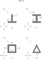
- FIG. 27 shows a modification of the position confirmation mark 45.
- the position confirmation mark 45 has a main scanning direction portion 451 and a sub scanning direction portion 452, and the main scanning direction portion 451 and the sub scanning direction portion 452 intersect each other. is doing. However, in this example, the central portion of the main scanning direction portion 451 and one end portion of the sub scanning direction portion 452 intersect each other.
- the position confirmation mark 45 has two main scanning direction portions 451 and one sub scanning direction portion 452, and the two main scanning direction portions 451 and the sub scanning direction.
- the portion 452 intersects with each other.
- the center portion of the two main scanning direction portions 451 and the both end portions of the sub scanning direction portion 452 intersect each other.
- the position confirmation mark 45 has two main scanning direction portions 451 and two sub scanning direction portions 452, and includes two main scanning direction portions 451 and two sub scanning direction portions 451.
- the scanning direction portion 452 intersects with each other.
- both end portions of the two main scanning direction portions 451 intersect with both end portions of the sub-scanning direction portion 452.
- the position confirmation mark 45 of this example has a rectangular shape.
- the position confirmation mark 45 has one main scanning direction portion 451 and two oblique sides, and has a triangular shape as a whole.
- the position confirmation mark 45 is not particularly limited in shape as long as it can serve as a reference for relative positioning in mounting the thermal print head 101 to the printer. .
- the main scanning direction portion 451 positioning in the sub scanning direction can be performed more accurately, and by having the sub scanning direction portion 452, positioning in the main scanning direction can be performed accurately.
- the configuration is not limited to the configuration having the main scanning direction portion 451 and the sub scanning direction portion 452.
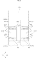
- FIG. 28 is an enlarged plan view of a main part of the thermal print head according to the second embodiment of the present invention.
- FIG. 29 is an enlarged cross-sectional view of a main part along the line XXIX-XIXX in FIG.
- the thermal print head 102 shown in the figure further includes a test electrode layer 38.
- the test electrode layer 38 is electrically connected to the position confirmation mark 45.
- the test electrode layer 38 is made of the same material as the electrode layer 3, and is formed together with the electrode layer 3 in the above-described manufacturing method.
- the test electrode layer 38 has two wiring portions 381 and two test pads 382.
- the wiring portion 381 is a portion connected to the position confirmation mark 45, and has a strip shape in this embodiment.
- the two wiring portions 381 are connected to both ends in the X direction of the sub-scanning direction portion 452 of the position confirmation mark 45.
- the test pad 382 is connected to the end of the wiring portion 381 opposite to the end connected to the position confirmation mark 45.
- the test pad 382 is a portion wider than the wiring portion 381.
- the sub-scanning direction part 452 of the position confirmation mark 45 and the wiring part 381 of the test electrode layer 38 overlap each other, and the test part 55 is interposed therebetween.
- the test part 55 is made of the same material as the insulating layer 5 described above, and is manufactured together with the insulating layer 5.
- the test portion 55 is provided to accurately define which position of the sub-scanning direction portion 452 of the position confirmation mark 45 the wiring portion 381 of the test electrode layer 38 contacts with the position confirmation mark 45. In FIG. 28, the test unit 55 is omitted.
- the test unit 55 has a plurality of openings 551.
- the plurality of openings 551 are provided in a portion of the test portion 55 that overlaps the sub-scanning direction portion 452 of the position confirmation mark 45, and are arranged separately at both ends of the sub-scanning direction portion 452.
- the opening 551 is filled with a part of the wiring portion 381 of the wiring portion 381. Thereby, the wiring portion 381 of the test electrode layer 38 is in contact with the sub-scanning direction portion 452 of the position confirmation mark 45 through the opening 551 of the test portion 55.
- the position confirmation mark 45 it is possible to diagnose whether the resistance value of the resistor layer 4 is appropriate. For example, two resistance measurement probes (not shown) are brought into contact with two test pads 382, and a current is passed from these probes to the position confirmation mark 45. Thereby, the resistance value of the position confirmation mark 45 can be measured. Since the position confirmation mark 45 is formed together with the resistor layer 4, the material and thickness thereof are the same as those of the resistor layer 4. Further, the position confirmation mark 45 is patterned by etching using photolithography in the same manner as the resistor layer 4. For this reason, the planar view dimension of the position confirmation mark 45 is known. For this reason, it is possible to diagnose whether the measured resistance value of the position confirmation mark 45 is an appropriate value for the resistance value assumed from the material, thickness, and planar size of the position confirmation mark 45.
- FIG. 30 is an enlarged plan view of the main part of the thermal print head according to the third embodiment of the present invention.
- the thermal print head 103 shown in the figure has a position confirmation mark 45 and a test electrode layer 38 in the same manner as the thermal print head 102.
- the main scanning direction portion 451 and the sub-scanning direction portion 452 of the position confirmation mark 45 are separated from each other and are disposed with a gap therebetween.
- the main scanning direction portion 451 of the present embodiment is configured by two regions separated in the y direction.
- the sub-scanning direction part 452 is composed of one area. According to the definition that the main scanning direction portion 451 is constituted by two regions, it can be said that the main scanning direction portion 451 and the sub scanning direction portion 452 also intersect each other in this embodiment. Further, it can be said that the main scanning direction portion 451 and the sub scanning direction portion 452 intersect each other at the center portion.
- the resistance value can be diagnosed using the position confirmation mark 45.
- only the sub-scanning direction part 452 of the position confirmation mark 45 is electrically connected to the test electrode layer 38.
- the sub-scanning direction portion 452 has a strip shape extending in the X direction. Therefore, the portion of the position confirmation mark 45 that is energized through the test electrode layer 38 has a simpler shape. This makes it easier to assume the resistance value of the position confirmation mark 45 (sub-scanning direction portion 452).
- the shape of the sub-scanning direction portion 452 is similar to the shape of the heat generating portion 41 of the resistor layer 4. Therefore, the resistance value of the heat generating portion 41 can be estimated more accurately by measuring the resistance value of the position confirmation mark 45 (sub-scanning direction portion 452).
- the present invention is not limited to the embodiment described above.
- the specific configuration of each part of the present invention can be changed in various ways.
Landscapes
- Electronic Switches (AREA)
Abstract
本発明のサーマルプリントヘッド101は、半導体よりなる基材11と、基材11に支持され且つ通電によって発熱する発熱部41を有する抵抗体層4と、基材11に形成され且つ抵抗体層4と導通する電極層3と、絶縁層5と、を備え、基材11に支持され且つ抵抗体層4と同じ材質よりなる位置確認マーク45が形成されている。これにより、プリンタへの取り付け精度を向上させることが可能である。
Description
本発明は、サーマルプリントヘッド、および、サーマルプリントヘッドの製造方法に関する。
従来から知られているサーマルプリントヘッドは、基板と、グレーズ層と、発熱抵抗体と、電極と、を備える。このようなサーマルプリントヘッドは、たとえば特許文献1に開示されている。同文献に開示のサーマルプリントヘッドにおいて、グレーズ層は基板に形成されている。グレーズ層は、発熱抵抗体にて発生した熱を蓄熱する役割を果たす。発熱抵抗体は、グレーズ層に形成されている。電極は、互いに離間した2つの部分を有する。これらの2つの部分に跨るように、発熱抵抗体には、発熱部が形成されている。
サーマルプリントヘッドは、プリンタに組み込まれるものであり、プリンタの印字品質を決定づける基幹モジュールである。このため、サーマルプリントヘッドのプリンタに対する取り付け精度が重要である。
本発明は、上記した事情のもとで考え出されたものであって、プリンタへの取り付け精度を向上させることが可能なサーマルプリントヘッドおよびサーマルプリントヘッドの製造方法を提供することをその主たる課題とする。
本発明の第1の側面によって提供されるサーマルプリントヘッドは、半導体よりなる基材と、前記基材に支持され且つ通電によって発熱する発熱部を有する抵抗体層と、前記基材に形成され且つ前記抵抗体層と導通する電極層と、絶縁層と、を備え、前記基材に支持され且つ前記抵抗体層と同じ材質よりなる位置確認マークが形成されている。
本発明の好ましい実施の形態においては、前記電極層は、互いに離間する第1導電部および第2導電部を含み、前記発熱部は、前記基材の厚さ方向視において、前記第1導電部および前記第2導電部に跨っている。
本発明の好ましい実施の形態においては、前記絶縁層は、前記電極層および前記発熱部の間に介在している部分を有する。
本発明の好ましい実施の形態においては、前記絶縁層は、第1介在部と第2介在部とを有し、前記第1介在部は、前記第1導電部および前記発熱部の間に介在しており、前記第2介在部は、前記第2導電部および前記発熱部の間に介在している。
本発明の好ましい実施の形態においては、前記絶縁層は、前記基材の厚さ方向視において、前記第1介在部と前記第2介在部とに挟まれた中間部を有し、前記中間部は、前記第1介在部および前記第2介在部につながっている。
本発明の好ましい実施の形態においては、前記第1介在部には、第1開口が形成されており、前記発熱部は、前記第1導電部の一部に直接接する第1当接部を有し、前記第1当接部は、前記基材の厚さ方向視において、前記第1開口と重なる位置に位置している。
本発明の好ましい実施の形態においては、前記第1導電部の一部は、前記第1開口内に形成されている。
本発明の好ましい実施の形態においては、前記第2介在部には、第2開口が形成されており、前記発熱部は、前記第2導電部の一部に直接接する第2当接部を有し、前記第2当接部は、前記基材の厚さ方向視において、前記第2開口と重なる位置に位置している。
本発明の好ましい実施の形態においては、前記第2導電部の一部は、前記第2開口内に形成されている。
本発明の好ましい実施の形態においては、前記抵抗体層は、前記第2導電部の位置する側とは反対側を向く第1端面を有し、前記絶縁層は、前記第1介在部につながり且つ前記第1端面を覆う部分を含む。
本発明の好ましい実施の形態においては、前記抵抗体層は、前記第1導電部の位置する側とは反対側を向く第2端面を有し、前記絶縁層は、前記第2介在部につながり且つ前記第2端面を覆う部分を含む。
本発明の好ましい実施の形態においては、前記抵抗体層および前記位置確認マークと前記基板との間に介在する蓄熱層を備える。
本発明の好ましい実施の形態においては、前記抵抗体層および前記位置確認マークは、前記蓄熱層に直接接している。
本発明の好ましい実施の形態においては、前記抵抗体層、前記電極層および前記絶縁層を覆う保護層を更に備えており、前記位置確認マークは、前記保護層から露出している。
本発明の好ましい実施の形態においては、前記保護層は、不透明である。
本発明の好ましい実施の形態においては、前記保護層は、黒色である。
本発明の好ましい実施の形態においては、前記保護層は、SiAlON、SiCおよびCSiCの少なくともいずれかよりなる。
本発明の好ましい実施の形態においては、前記位置確認マークは、主走査方向に延びる主走査方向部と、副走査方向に延びる副走査方向部と、を有する。
本発明の好ましい実施の形態においては、前記主走査方向部と前記副走査方向部とは、互いに交差している。
本発明の好ましい実施の形態においては、前記主走査方向部と前記副走査方向部とは、互いの中央部分において交差している。
本発明の好ましい実施の形態においては、前記位置確認マークに導通するテスト電極層を備える。
本発明の好ましい実施の形態においては、前記テスト電極層は、前記電極層と同じ材質よりなる。
本発明の好ましい実施の形態においては、前記テスト電極層は、前記位置確認マークに繋がる配線部と、この配線部に繋がるテスト用パッド部と、を含む。
本発明の好ましい実施の形態においては、前記配線部は、前記副走査方向部の副走査方向両端に繋がっている。
本発明の好ましい実施の形態においては、前記副走査方向部と前記主走査方向部とは、互いに離間している。
本発明の好ましい実施の形態においては、配線基板と、複数のワイヤと、前記配線基板、前記複数のワイヤ、および、前記保護層を覆う樹脂層と、を更に備える。
本発明の好ましい実施の形態においては、前記保護層には、貫通窓が形成されており、前記電極層は、前記貫通窓から露出するボンディング部を含み、前記ボンディング部には、前記複数のワイヤのいずれかがボンディングされている。
本発明の好ましい実施の形態においては、前記樹脂層は、前記保護層に直接接している。
本発明の好ましい実施の形態においては、前記電極層に電流を流す駆動ICを更に備え、前記駆動ICは、前記配線基板に搭載されている。
本発明の好ましい実施の形態においては、前記絶縁層は、SiO2またはSiAlO2よりなる。
本発明の好ましい実施の形態においては、前記抵抗体層は、ポリシリコン、TaSiO2、および、TiONの少なくともいずれかよりなる。
本発明の好ましい実施の形態においては、前記電極層は、Au、Ag、Cu、Cr、Al-Si、および、Tiの少なくともいずれかよりなる。
本発明の好ましい実施の形態においては、前記電極層は、前記発熱部に直接接するバリアメタル層を含む。
本発明の第2の側面によって提供されるサーマルプリントヘッドの製造方法は、本発明の第1の側面によって提供されるサーマルプリントヘッドの製造方法であって、前記基材に前記抵抗体層と前記位置確認マークとを一括して形成する工程と、前記基材に前記電極層を形成する工程と、を備える。
本発明の好ましい実施の形態においては、前記抵抗体層を形成する工程は、CVDまたはスパッタにより行う。
本発明の好ましい実施の形態においては、前記抵抗体層は、ポリシリコン、TaSiO2、および、TiONの少なくともいずれかよりなる。
本発明の好ましい実施の形態においては、前記電極層を形成する工程は、CVDまたはスパッタにより行う。
本発明のその他の特徴および利点は、添付図面を参照して以下に行う詳細な説明によって、より明らかとなろう。
以下、本発明の実施の形態につき、図面を参照して具体的に説明する。
<第1実施形態>
図1~図26を用いて、本発明の第1実施形態について説明する。
図1~図26を用いて、本発明の第1実施形態について説明する。
図1は、本発明の第1実施形態のサーマルプリントヘッドの平面図である。図2は、図1のII-II線に沿う断面図である。なお、以降の説明において、X方向は、副走査方向であり、Y方向は、主走査方向である。
これらの図に示すサーマルプリントヘッド101は、基材11と、配線基板12と、放熱板13と、蓄熱層2と、電極層3と、抵抗体層4と、位置確認マーク45と、絶縁層5と、保護層6(図1では省略)と、駆動IC7と、複数のワイヤ81と、封止樹脂82と、コネクタ83とを備える。サーマルプリントヘッド101は、印刷媒体801に印刷を施すプリンタに組み込まれるものである。このような印刷媒体801としては、たとえばバーコードシートやレシートを作成するための感熱紙が挙げられる。
図2に示す放熱板13は、基材11からの熱を放散させるためのものである。放熱板13は、たとえばAlなどの金属よりなる。放熱板13には基材11および配線基板12が取り付けられている。
基材11は板状を呈している。本実施形態においては、基材11は半導体材料よりなる。基材11を構成する半導体材料としては、たとえば、Si、SiC、AlN、GaP、GaAs、InP、およびGaNが挙げられる。以下に述べる構成に好ましい基材11の材質としては、Siが挙げられる。基材11の厚さはたとえば0.625~0.720mmである。図1に示すように、基材11は、方向Yに長く延びる平板状である。基材11の幅(基材11の方向Xにおける寸法)は、たとえば、3~20mmである。基材11の方向Yにおける寸法は、たとえば、10~300mmである。
図3は、図1に示したサーマルプリントヘッド101を模式的に表す部分拡大平面図(一部構成省略)である。図6は、図3のVI-VI線に沿う部分拡大断面図である。図7は、サーマルプリントヘッド101の構成要素の形状をより忠実に表す部分拡大要部平面図である。図3では、保護層6、および、封止樹脂82を省略している。図7では、絶縁層5、保護層6、および、封止樹脂82を省略している。
図6に示すように、基材11は基材表面111を有する。基材表面111は、方向Xと方向Yとに広がる平面状である。基材表面111は、方向Yに沿って長手状に延びる。基材表面111は、基材11の厚さ方向Zの一方(以下、方向Zaと言う。図6では上方)を向く。すなわち、基材表面111は、抵抗体層4の位置する側を向く面である。
図2、図6に示すように、蓄熱層2は基材11に形成されている。蓄熱層2は、基材11の基材表面111の全体を覆っている。蓄熱層2は、発熱部41(後述)にて発生した熱を蓄えるためのものである。蓄熱層2の厚さは、たとえば、3μm以上である。図6に示すように、蓄熱層2は蓄熱層表面21を有する。蓄熱層表面21は方向Zaを向く。すなわち、蓄熱層表面21は、抵抗体層4の位置する側を向く面である。本実施形態では、蓄熱層表面21は全体にわたって平坦である。蓄熱層表面21が平坦であると、半導体プロセスによって抵抗体層4や絶縁層5を形成しやすい。
図2、図6に示すように、本実施形態では、蓄熱層2は、第1層26と第2層27とを含む。第1層26は、第2層27と基材11との間に位置している。第1層26は、基材11を構成する半導体材料を酸化した材料よりなる層である。たとえば、基材11を構成する半導体材料がSiである場合には、第1層26はSiO2よりなる層である。第2層
27は絶縁材料よりなる層である。第2層27を構成する材料は、特に限定されないが、本実施形態においては、第1層26を構成する材料と同一の材料よりなる。本実施形態とは異なり、蓄熱層2が二層構造ではなく、一層構造であってもよい。
27は絶縁材料よりなる層である。第2層27を構成する材料は、特に限定されないが、本実施形態においては、第1層26を構成する材料と同一の材料よりなる。本実施形態とは異なり、蓄熱層2が二層構造ではなく、一層構造であってもよい。
図2、図3、図6、図7に示す電極層3は基材11に形成されている。図3および図7における電極層3には、理解の便宜上、ハッチを付している。具体的には、電極層3は蓄熱層2に積層されている。また、電極層3は抵抗体層4に積層されている。本実施形態においては、電極層3と蓄熱層2との間に、抵抗体層4が介在している。電極層3は、抵抗体層4に導通している。電極層3は、抵抗体層4に通電するための経路を構成している。電極層3を構成する材料としては、たとえば、Au、Ag、Cu、Cr、Al-Si、および、Tiが挙げられる。本実施形態とは異なり、電極層3は、蓄熱層2と抵抗体層4との間に介在していてもよい。
図4は、図3の領域IVの部分拡大平面図である。図5は、図4から、電極層3を省略して示す平面図である。なお、図6は、図4のVI-VI線に沿う断面図に相当する。
図4、図6に示すように、電極層3は、第1導電部31と第2導電部32とを含む。第1導電部31および第2導電部32は、互いに離間している。第1導電部31と第2導電部32の離間寸法は、たとえば、105μmである。
本実施形態においては、図3および図7に示すように、電極層3は、複数の個別電極33(同図には6つ示す)と、一つの共通電極35と、複数の中継電極37(同図には6つ示す)とを含む。より具体的には、次のとおりである。
複数の個別電極33は、互いに導通していない。そのため、各個別電極33には、サーマルプリントヘッド101の組み込まれたプリンタが使用される際に、個別に、互いに異なる電位が付与されうる。各個別電極33は、個別電極帯状部331と、屈曲部333と、直行部334と、斜行部335と、ボンディング部336とを有する。図4、図6に示すように、各個別電極帯状部331は、電極層3における第1導電部31を構成しており、方向Xに沿って延びる帯状である。各個別電極帯状部331は、抵抗体層4に積層されている。屈曲部333は、個別電極帯状部331につながり、方向Yおよび方向Xのいずれに対しても傾斜している。直行部334は、方向Xに平行にまっすぐ延びている。斜行部335は、方向Yおよび方向Xのいずれに対しても傾斜した方向に延びている。ボンディング部336は、ワイヤ81がボンディングされる部分である。本実施形態においては、個別電極帯状部331、屈曲部333、直行部334、および斜行部335の幅が、たとえば47.5μm程度であり、ボンディング部336の幅がたとえば80μm程度である。
共通電極35は、サーマルプリントヘッド101の組み込まれたプリンタが使用される際に複数の個別電極33に対して電気的に逆極性となる部位である。共通電極35は、複数の共通電極帯状部351と、複数の分岐部353と、複数の直行部354と、複数の斜行部355と、複数の延出部356と、一つの基幹部357とを有する。各共通電極帯状部351は、方向Xに延びる帯状である。図4、図6に示すように、各共通電極35において、複数の共通電極帯状部351は、電極層3における第1導電部31を構成しており、方向Yに互いに離間し、且つ、互いに導通している。各共通電極帯状部351は、抵抗体層4に積層されている。各共通電極帯状部351は、個別電極帯状部331と方向Yに離間している。本実施形態においては、互いに隣接した2つずつの共通電極帯状部351が、2つの個別電極帯状部331に挟まれている。複数の共通電極帯状部351、および複数の個別電極帯状部331は、方向Yに沿って配列されている。分岐部353は、2つの共通電極帯状部351と1つの直行部354をつなぐ部分であり、Y字状である。直行部354は、方向Xに平行にまっすぐ延びている。斜行部355は、方向Yおよび方向Xのいずれに対しても傾斜した方向に延びている。延出部356は、斜行部355につながり、方向Xに沿って延びている。基幹部357は、方向Yに延びる帯状であり、複数の延出部356がつながっている。本実施形態においては、共通電極帯状部351、直行部354、斜行部355、および延出部356の幅が、たとえば47.5μm程度である。
複数の中継電極37はそれぞれ、複数の個別電極33のうちの一つと共通電極35との間に電気的に介在する。各中継電極37は、2つの中継電極帯状部371と連結部373とを有する。図4、図6に示すように、各中継電極帯状部371は、電極層3における第2導電部32を構成しており、方向Xに延びる帯状である。すなわち、電極層3における第2導電部32と第1導電部31とは、互いに離間しており、本実施形態においては、方向Xに互いに離間している。複数の中継電極帯状部371は、方向Yに互いに離間している。各中継電極帯状部371は、抵抗体層4に積層されている。複数の中継電極帯状部371は、抵抗体層4上において、複数の帯状部331,351とは方向Xにおいて反対側に配置されている。各中継電極37における2つの中継電極帯状部371の一方は、複数の共通電極帯状部351のいずれか一つと、方向Xに互いに離間している。各中継電極37における2つの中継電極帯状部371の他方は、複数の個別電極帯状部331のいずれか一つと、方向Xに互いに離間している。複数の連結部373はそれぞれ、方向Yに沿って延びている。各連結部373は、各中継電極37における2つの中継電極帯状部371につながる。これにより、各中継電極37における2つの中継電極帯状部371どうしが互いに導通している。
なお、電極層3は、必ずしも中継電極37を含む必要はなく、たとえば、複数の個別電極と、これらの個別電極に隣接する共通電極と、を含むものであってもよい。
図2~図7に示す抵抗体層4は基材11に形成されている。本実施形態では、抵抗体層4は、蓄熱層2に直接形成されている。本実施形態においては、抵抗体層4は、複数の矩形状の部分を有する。抵抗体層4は、電極層3からの電流が流れた部分が発熱する。このように発熱することによって印字ドットが形成される。抵抗体層4は、電極層3を構成する材料よりも抵抗率が高い材料よりなる。抵抗体層4を構成する材料としては、たとえば、ポリシリコン、TaSiO2、および、TiONが挙げられる。本実施形態においては、抵抗体層4には、抵抗値の調整のため、イオン(たとえば、ホウ素)がドーピングされている。抵抗体層4の厚さは、たとえば、0.2μm~1μmである。
図4~図6に示すように、抵抗体層4は、第1端面416と、第2端面417とを有する。
図4~図6に示すように、第1端面416は、第2導電部32(中継電極帯状部371)の位置する側とは反対側(すなわち、図6の右方向)を向いている。第2端面417は、第1導電部31(個別電極帯状部331もしくは共通電極帯状部351)の位置する側とは反対側(すなわち、図6の左方向)を向いている。
図6に示すように、抵抗体層4は、サーマルプリントヘッド101の使用時に発熱する発熱部41を含む。図4、図5に示すように、発熱部41は、基材11の厚さ方向視において、第1導電部31および第2導電部32に跨っている。各発熱部41は蓄熱層2に積層されている。
図6に示すように、発熱部41は、第1当接部411および第2当接部412を含んでいる。第1当接部411は、電極層3における第1導電部31に当接している。第2当接部412は、電極層3における第2導電部32に当接している。
図6に示すように、絶縁層5は、発熱部41および電極層3の間に介在している部分を有する。絶縁層5を構成する材料としては、たとえば、SiO2、および、SiAlO2が挙げられる。絶縁層5は、第1介在部51と、第2介在部52と、中間部53とを含む。図4~図6に示すように、第1介在部51は、第1導電部31および発熱部41の間に介在している部位である。第2介在部52は、第2導電部32および発熱部41の間に介在している。中間部53は、基材11の厚さ方向Z視において、第1介在部51と第2介在部52とに挟まれている。中間部53は、第1介在部51および第2介在部52につながっている。
図4~図6に示すように、本実施形態において、第1介在部51には、少なくとも1以上の第1開口511が形成されている。図4、図5にて第1開口511は円形状である例を示しているが、第1開口511の形状は円形状に限られない。たとえば、第1開口511は矩形状であってもよい。図4、図5にて第1介在部51に第1開口511が複数形成されている例を示しているが、第1介在部51に形成されている第1開口511の個数は、1つであってもよい。第1開口511と重なる位置に、上述の発熱部41における第1当接部411が位置している。図6に示すように、本実施形態においては更に、第1開口511内に、第1導電部31の一部が形成されている。
本実施形態において、第2介在部52には、少なくとも1以上の第2開口521が形成されている。図4、図5にて第2開口521は円形状である例を示しているが、第2開口521の形状は円形状に限られない。たとえば、第2開口521は矩形状であってもよい。図4、図5にて第2介在部52に第2開口521が複数形成されている例を示しているが、第2介在部52に形成されている第2開口521の個数は、1つであってもよい。第2開口521と重なる位置に、上述の発熱部41における第2当接部412が位置している。図6に示すように、本実施形態においては更に、第2開口521内に、第2導電部32の一部が形成されている。
図4~図6に示すように、本実施形態においては、絶縁層5は、部分581,582を含む。部分581は、第1介在部51につながり且つ第1端面416を覆う部分である。部分582は、第2介在部52につながり且つ第2端面417を覆う部分である。部分581,582はそれぞれ、蓄熱層2に直接接している。すなわち、絶縁層5に直接接する部分を、蓄熱層2が有している。本実施形態とは異なり、絶縁層5が部分581,582を含んでいなくてもよい。
図2、図6に示す保護層6は、電極層3と抵抗体層4と絶縁層5とを覆っており、電極層3と抵抗体層4と絶縁層5とを保護するためのものである。保護層6は、絶縁材料よりなる。保護層6を構成する絶縁材料としては、たとえば、SiAlON、SiCおよびCSiCが挙げられる。保護層6は、不透明であり、典型的には、黒色である。なお、本実施形態においては、保護層6と電極層3、抵抗体層4、絶縁層5および基材11との間には、下地保護層60が介在している。下地保護層60は、平面視において基材11のほぼ全域に形成されている。下地保護層60は、たとえばガラス等からなる透明な層である。ただし、たとえば導通を図るべき箇所等においては、下地保護層60に適宜開口が設けられている。また、図2および図8を除き、理解の便宜上、下地保護層60を省略し、適宜説明を省略する。図8において、濃いハッチングが施された領域が、保護層6を示しており、薄いハッチングが施された領域が、下地保護層60を示している。同図に示すように、保護層6は、位置確認マーク45を露出させている。また、下地保護層60は、位置確認マーク45を覆っている。
保護層6には、複数の貫通窓61(図2には1つ示す)が形成されている。各貫通窓61からは、ボンディング部336が露出している。
位置確認マーク45は、基材11に支持されており、たとえばポリシリコンなどの抵抗体層4と同じ材質からなる。本実施形態においては、位置確認マーク45は、蓄熱層2上に形成されており、蓄熱層2に直接接している。図1および図8に示すように、本実施形態においては、2つの位置確認マーク45が、基材11のY方向両端付近に設けられている。保護層6が黒色などの不透明なものである場合、位置確認マーク45は、保護層6から露出している。保護層6が透明である場合、位置確認マーク45は保護層6に覆われていてもよい。位置確認マーク45は、サーマルプリントヘッド101をプリンタに取り付ける際に、プリンタに対するサーマルプリントヘッド101の相対位置を特定するためのマークとして用いられる。このため、位置確認マーク45は、肉眼による目視、あるいは撮像手段による画像解析が可能となるように、基材11もしくは蓄熱層2に対してコントラストを生じうる外観を有する。
図9は、位置確認マーク45を示す要部拡大平面図である。図10は、図9のX-X線に沿う要部拡大断面図である。同図に示すように、位置確認マーク45は、主走査方向部451および副走査方向部452を有している。主走査方向部451は、主走査方向であるY方向に延びている。副走査方向部452は、副走査方向であるX方向に延びている。主走査方向部451と副走査方向部452とは、一体的に形成されている。主走査方向部451と副走査方向部452とは、互いに交差している。より具体的には、主走査方向部451と副走査方向部452とは、互いの中央部分において交差している。
図2に示す配線基板12は、たとえば、プリント配線基板である。配線基板12は、基材層と図示しない配線層とが積層された構造を有する。基材層は、たとえばガラスエポキシ樹脂よりなる。配線層は、たとえばCuよりなる。
図2、図3に示す駆動IC7は、各個別電極33にそれぞれ電位を付与し、各発熱部41に流す電流を制御するものである。各個別電極33にそれぞれ電位が付与されることにより、共通電極35と各個別電極33との間に電圧が印加され、各発熱部41に選択的に電流が流れる。駆動IC7は、配線基板12に搭載されている。図3に示すように、駆動IC7は、複数のパッド71を含む。複数のパッド71は、たとえば、2列に形成されている。なお、複数のパッド71は、3列あるいは4列に形成されていてもよい。
図2、図3に示す複数のワイヤ81は、たとえば、Auなどの導体よりなる。複数のワイヤ81のうちワイヤ811はそれぞれ、駆動IC7にボンディングされ、且つ、電極層3にボンディングされている。より具体的には、各ワイヤ811は、駆動IC7におけるパッド71にボンディングされ、且つ、ボンディング部336にボンディングされている。これにより、駆動IC7と各個別電極33とが導通している。図3に示すように、複数のワイヤ81のうちワイヤ812は、それぞれ、駆動IC7におけるパッド71にボンディングされ、且つ、配線基板12における配線層にボンディングされている。これにより、当該配線層を介して、駆動IC7とコネクタ83とが導通している。同図に示すように、複数のワイヤ81のうちワイヤ813は、共通電極35における基幹部357にボンディングされ、且つ、配線基板12における配線層にボンディングされている。これにより、共通電極35と上記配線層とが導通している。
図2に示す封止樹脂82は、たとえば、黒色の樹脂よりなる。封止樹脂82は、駆動IC7、複数のワイヤ81、および、保護層6を覆っており、駆動IC7および複数のワイヤ81を保護している。封止樹脂82は保護層6に直接接する。コネクタ83は、配線基板12に固定されている。コネクタ83は、サーマルプリントヘッド101の外部からサーマルプリントヘッド101へ電力を供給し、駆動IC7を制御するためのものである。
次に、サーマルプリントヘッド101の使用方法の一例について簡単に説明する。
サーマルプリントヘッド101は、プリンタに組み込まれた状態で使用される。図2に示したように、当該プリンタ内において、サーマルプリントヘッド101の各発熱部41はプラテンローラ802に対向している。当該プリンタの使用時には、プラテンローラ802が回転することにより、印刷媒体801が、方向Xに沿ってプラテンローラ802と各発熱部41との間に一定速度で送給される。印刷媒体801は、プラテンローラ802によって保護層6のうち各発熱部41を覆う部分に押しあてられる。一方、図3に示した各個別電極33には、駆動IC7によって選択的に電位が付与される。これにより、共通電極35と複数の個別電極33の各々との間に電圧が印加される。そして、複数の発熱部41には選択的に電流が流れ、熱が発生する。そして、各発熱部41にて発生した熱は、保護層6を介して印刷媒体801に伝わる。そして、印刷媒体801上の方向Yに線状に延びる第1ライン領域に、複数のドットが印刷される。また、各発熱部41にて発生した熱は、蓄熱層2にも伝わり、蓄熱層2にて蓄えられる。
更に、プラテンローラ802が回転することにより、印刷媒体801が、方向Xに沿って一定速度で引き続き送給される。そして、上述の第1ライン領域への印刷と同様に、印刷媒体801上の方向Yに線状に延びる、第1ライン領域に隣接する第2ライン領域への印刷が行われる。第2ライン領域への印刷の際、印刷媒体801には、各発熱部41にて発生した熱に加え、第1ライン領域への印刷時に蓄熱層2にて蓄えられた熱が伝わる。このようにして、第2ライン領域への印刷が行われる。以上のように、印刷媒体801上の方向Yに線状に延びるライン領域ごとに、複数のドットを印刷することにより、印刷媒体801への印刷が行われる。
次に、サーマルプリントヘッド101の製造方法の一例について簡単に説明する。本実施形態においてサーマルプリントヘッド101を製造するには、半導体プロセスを用いる。
まず、図11に示すように、半導体基板19を用意する。本実施形態において半導体基板19はSiよりなる。次に、図12に示すように、半導体基板19の表面を熱酸化する。これにより、基材11と、基材11に積層された第1層26とが形成される。本実施形態においては、第1層26は、SiO2よりなる。次に、図13に示すように、CVDもしくはスパッタによって、第1層26上に第2層27を形成する。これにより、基材11に積層された蓄熱層2が形成される。図示することは省略するが、基材11の裏面にもSiO2層が形成される。なお、本実施形態とは異なり、半導体基板19の表面を熱酸化する必要は必ずしもなく、CVDもしくはスパッタによって、直接、蓄熱層2を形成してもよい。
次に、図14に示すように、抵抗体層4’を形成する。抵抗体層4’の形成は、たとえば、CVDもしくはスパッタにより行う。抵抗体層4’は、基材11の表面の全面に形成する。次に、図15、図16に示すように、抵抗体層4’をエッチングすることにより、抵抗体層4’’を形成する。抵抗体層4’のエッチングは、フォトリソグラフィーにより行う。図16に示すように、本実施形態では、抵抗体層4’’は、一方向に沿って帯状に延びる帯状部分と、基材11のY方向両端付近に相当する位置に配置された十字状部分と、を有する。前記帯状部分は、複数の発熱部41を含む抵抗体層4となる部位である。前記十字状部分は、位置確認マーク45となる部位である。次に、抵抗体層4が所望の抵抗値になるように、抵抗体層4’’にイオンを打ち込む(図示略)。このイオンの打ち込みは、前記帯状部分だけでなく、十字状部分にも行う。
次に、図17に示すように、絶縁層5’を形成する。絶縁層5’の形成は、たとえば、CVDもしくはスパッタにより行う。次に、図18、図19に示すように、絶縁層5’をエッチングすることにより、上述の絶縁層5を形成する。絶縁層5’をエッチングする当該工程を経ることにより、上述の第1開口511および第2開口521が形成される。
次に、図20、図21に示すように、電極層3’を形成する。電極層3’の形成は、たとえば、スパッタもしくはCVDにより行う。次に、図22、図23に示すように、電極層3’をエッチングすることにより、上述の形状の電極層3を形成する。電極層3’のエッチングは、フォトリソグラフィーにより行う。
次に、図24に示すように、抵抗体層4’’をエッチングすることにより、複数の矩形状の部分を有する上述の抵抗体層4が形成される。これは、サーマルプリントヘッド101の使用時において、抵抗体層4内を図24の横方向に電流が流れることを防止するためである。このエッチングにおいては、抵抗体材料層4’’の前記十字状部分は、処理がなされない。なお、本実施形態とは異なり、帯状の抵抗体層4’’を形成することなく、抵抗体層4’を一度エッチングすることにより、複数の矩形状の部分を有する上述の抵抗体層4を形成してもよい。また、抵抗体材料層4’’を形成するためのエッチングにおいては、前記十字状部分を形成せず、図23から図24に示す状態とするためのエッチングにおいて、前記十字状部分、すなわち位置確認マーク45を形成してもよい。
次に、図25に示すように、保護層6’を形成する。保護層6’の形成は、たとえば、CVDにより行う。次に、図26に示すように、保護層6’をエッチングすることにより、複数の貫通窓61を形成する。保護層6’のエッチングは、フォトリソグラフィーにより行う。なお、保護層6の形成に先立ち、上述した下地保護層60を形成しておく。
次に、図示は省略するが、基材11の裏面を研磨することにより、基材11の厚みを低減させる。次に、抵抗体層4の抵抗値の測定、および、基材11のダイシングを行ったのち、ダイシング後の製品と、配線基板12とを放熱板13に配置する。次に、図2に示した、駆動IC7を配線基板12に搭載し、ワイヤ81を所望の箇所にボンディングし、封止樹脂82を形成する。これらの工程を経るなどして、図2に示したサーマルプリントヘッド101が製造される。
次に、本実施形態の作用効果について説明する。
本実施形態においては、基材11に位置確認マーク45が形成されている。位置確認マーク45は、抵抗体層4と同じ材質からなり、抵抗体層4とともに一括して形成される。このため、位置確認マーク45と抵抗体層4の発熱部41との位置関係が正確に特定されやすい。サーマルプリントヘッド101をプリンタに取り付ける際に、位置確認マーク45を位置合わせの基準として用いることにより、プリンタと抵抗体層4の発熱部41との相対位置をより正確に設定することが可能である。したがって、サーマルプリントヘッド101のプリンタに対する取り付け精度を向上させることができる。
抵抗体層4の形成と位置確認マーク45の形成とを同一のフォトリソグラフィーを用いた工程によって行うことにより、抵抗体層4と位置確認マーク45との相対位置をより正確に設定することができる。
保護層6が、SiAlON、SiCおよびCSiCの少なくともいずれかよりなる場合、抵抗体層4等をより適切に保護することができる。抵抗体層4の保護に適した硬質な保護層6は、不透明、さらには黒色である場合がある。このような場合、位置確認マーク45を保護層6から露出させることにより、位置確認マーク45をサーマルプリントヘッド101の外観に明確に現出させることができる。
位置確認マーク45が、主走査方向部451と副走査方向部452とを有することにより、位置確認マーク45のX方向位置とY方向位置とのそれぞれをより正確に把握することができる。主走査方向部451と副走査方向部452とを交差させることにより、この交差点を位置決めの基準点として用いることができる。
本実施形態においては、サーマルプリントヘッド101は絶縁層5を備える。絶縁層5は、電極層3および発熱部41の間に介在している部分を有する。このような構成によると、電極層3と発熱部41とが接触する領域を小さくすることができる。そうすると、発熱部41に電流が流れて発熱した際に、電極層3と発熱部41とが共晶してしまう領域を小さくすることができる。電極層3と発熱部41とが共晶する領域を小さくできると、サーマルプリントヘッド101の使用時に、サーマルプリントヘッド101の抵抗値が変化してしまう不具合を抑制できる。
本実施形態においては、絶縁層5は、第1介在部51と第2介在部52とを有する。第1介在部51は、第1導電部31および発熱部41の間に介在している。このような構成によると、第1導電部31と発熱部41とが共晶することを、抑制できる。本実施形態においては、第2介在部52は、第2導電部32および発熱部41の間に介在している。このような構成によると、第2導電部32と発熱部41とが共晶することを、抑制できる。第1導電部31と発熱部41とが共晶すること、または、第2導電部32と発熱部41とが共晶することを防止できると、電極層3と発熱部41とが共晶する領域を小さくできる。これにより、サーマルプリントヘッド101の使用時に、サーマルプリントヘッド101の抵抗値が変化してしまう不具合を抑制できる。
仮に、電極層3が抵抗体層4と蓄熱層2との間に介在している場合には、抵抗体層4における発熱部41にて発生した熱は、電極層3に逃げてしまうおそれがある。電極層3に逃げてしまった熱は、印刷媒体801への伝熱には寄与しない。一方、本実施形態においては、抵抗体層4は、電極層3および蓄熱層2の間に介在している。このような構成によると、抵抗体層4における発熱部41にて発生した熱が電極層3に伝わっても、電極層3に伝わった熱は、印刷媒体801への伝熱に寄与しうる。そのため、発熱部41にて発生した熱をより効率的に、印刷媒体801に伝えることができる。すなわち、サーマルプリントヘッド101における印刷媒体801に接触する部位(保護層6)を、より速く、高温にすることが可能となる。これにより、印刷媒体801への高速印字が可能となる。
本実施形態では、基材11は、Siよりなる。Siは、熱伝導率が大きいため、発熱部41にて発生した熱を、より速く基材11の外部(本実施形態では放熱板13)へと伝えることができる。そのため、高温になった発熱部41の温度を、より速く、低下させることができる。このことは、印刷媒体801への印字の高速化に適する。
本実施形態では、保護層6における貫通窓61は、保護層6’をエッチングすることにより形成される。そうすると、保護層6における所望の部位に貫通窓61を形成することができるから、電極層3のうち保護層6に覆われていない部分を、封止樹脂82とは別の樹脂層(ソルダーレジスト層)で覆う必要がない。別の樹脂層(ソルダーレジスト層)を形成する必要がないことは、サーマルプリントヘッド101の製造効率の向上を図るのに適する。
以下の説明では、上記と同一もしくは類似の構成については上記と同一の符号を付し、説明を適宜省略する。
図27は、位置確認マーク45の変形例を示している。
図27(a)に示す変形例においては、位置確認マーク45は、主走査方向部451および副走査方向部452を有しており、主走査方向部451と副走査方向部452とは互いに交差している。ただし、本例においては、主走査方向部451の中央部分と、副走査方向部452の一端部分とが交差している。
図27(b)に示す変形例においては、位置確認マーク45は、2つの主走査方向部451および1つの副走査方向部452を有しており、2つの主走査方向部451と副走査方向部452とは互いに交差している。ただし、本例においては、2つの主走査方向部451の中央部分と、副走査方向部452の両端部分とが交差している。
図27(c)に示す変形例においては、位置確認マーク45は、2つの主走査方向部451および2つの副走査方向部452を有しており、2つの主走査方向部451と2つの副走査方向部452とは互いに交差している。ただし、本例においては、2つの主走査方向部451の両端部分と、副走査方向部452の両端部分とが交差している。これにより、本例の位置確認マーク45は、矩形状をなしている。
図27(d)に示す変形例においては、位置確認マーク45は、1つの主走査方向部451と、2つの斜辺部分とを有しており、全体として、三角形状とされている。
これらの変形例から理解されるように、位置確認マーク45は、サーマルプリントヘッド101のプリンタへの取り付けにおいて、相対的な位置決めを行うための基準となりうるものであれば、その形状は特に限定されない。主走査方向部451を有することにより、副走査方向における位置決めをより正確に行うことが可能であり、副走査方向部452を有することにより、主走査方向における位置決めを正確に行うことが可能であるが、主走査方向部451および副走査方向部452を有する構成に限定されるものではない。
<第2実施形態>
図28および図29を用いて、本発明の第2実施形態について説明する。
図28および図29を用いて、本発明の第2実施形態について説明する。
図28は、本発明の第2実施形態のサーマルプリントヘッドの要部拡大平面図である。図29は、図28のXXIX-XIXX線に沿う要部拡大断面図である。
同図に示すサーマルプリントヘッド102は、テスト電極層38をさらに備えている。テスト電極層38は、位置確認マーク45に導通している。テスト電極層38は、電極層3と同じ材質からなり、上述した製造方法において、電極層3と一括して形成される。
テスト電極層38は、2つの配線部381と2つのテスト用パッド382とを有する。配線部381は、位置確認マーク45に繋がる部分であり、本実施形態においては、帯状の形状とされている。2つの配線部381は、位置確認マーク45の副走査方向部452のX方向両端に繋がっている。テスト用パッド382は、配線部381のうち位置確認マーク45に繋がる端部とは反対側の端部に繋がっている。テスト用パッド382は、配線部381より幅が広い部分である。
本実施形態においては、位置確認マーク45の副走査方向部452とテスト電極層38の配線部381とが互いに重なり合っており、これらの間にテスト部55が介在している。テスト部55は、上述した絶縁層5と同じ材質からなり、絶縁層5と一括して製造される。テスト部55は、位置確認マーク45に対してテスト電極層38の配線部381が位置確認マーク45の副走査方向部452のいずれの箇所に接するかを正確に規定するために設けられている。なお、図28においては、テスト部55を省略している。
図29に示すように、テスト部55は、複数の開口551を有している。複数の開口551は、テスト部55のうち位置確認マーク45の副走査方向部452と重なる部分に設けられており、副走査方向部452の両端に分かれて配置されている。開口551内には、配線部381の配線部381の一部が充填された格好となっている。これにより、テスト電極層38の配線部381は、テスト部55の開口551を通して位置確認マーク45の副走査方向部452に接している。
本実施形態によっても、サーマルプリントヘッド102のプリンタに対する取り付け精度を向上させることができる。また、位置確認マーク45を用いた抵抗値測定を行うことにより、抵抗体層4の抵抗値が適正であるかの診断を行うことができる。たとえば、2つのテスト用パッド382に抵抗値測定用の2つのプローブ(図示略)を当接させ、これらのプローブから位置確認マーク45に電流を流す。これにより、位置確認マーク45の抵抗値を測定することができる。位置確認マーク45は、抵抗体層4と一括して形成されているため、材質や厚さが抵抗体層4と同一である。また、位置確認マーク45は、抵抗体層4と同様に、フォトリソグラフィーを用いたエッチングによってパターニングされている。このため、位置確認マーク45の平面視寸法は、既知である。このため、測定された位置確認マーク45の抵抗値が、位置確認マーク45の材質、厚さおよび平面視寸法から想定される抵抗値に対して適正な値であるかを診断することができる。
<第3実施形態>
図30を用いて、本発明の第3実施形態について説明する。
図30を用いて、本発明の第3実施形態について説明する。
図30は、本発明の第3実施形態のサーマルプリントヘッドの要部拡大平面図である。
同図に示すサーマルプリントヘッド103は、サーマルプリントヘッド102と同様に位置確認マーク45およびテスト電極層38を有する。本実施形態においては、位置確認マーク45の主走査方向部451と副走査方向部452とは、互いに離間しており、互いの間に隙間を隔てて配置されている。より具体的には、本実施形態の主走査方向部451は、y方向に離間する2つの領域によって構成されている。副走査方向部452は、1つの領域によって構成されている。主走査方向部451が2つの領域によって構成されたものであるとの定義により、本実施形態においても、主走査方向部451と副走査方向部452とは、互いに交差しているといえる。また、主走査方向部451と副走査方向部452とは、互いの中央部分において交差しているといえる。
本実施形態においても、サーマルプリントヘッド103のプリンタに対する取り付け精度を向上させることができる。また、位置確認マーク45を用いた抵抗値の診断を行うことができる。さらに、本実施形態においては、位置確認マーク45のうち副走査方向部452のみがテスト電極層38に導通する。副走査方向部452は、X方向に延びる帯状である。このため、位置確認マーク45のうちテスト電極層38を介して通電させる部分が、より単純な形状となる。これにより、位置確認マーク45(副走査方向部452)の抵抗値の想定がより容易となる。また、副走査方向部452の形状は、抵抗体層4の発熱部41の形状と類似する。したがって、位置確認マーク45(副走査方向部452)の抵抗値を測定することによって、発熱部41の抵抗値をより正確に推定することができる。
本発明は、上述した実施形態に限定されるものではない。本発明の各部の具体的な構成は、種々に設計変更自在である。
Claims (37)
- 半導体よりなる基材と、
前記基材に支持され且つ通電によって発熱する発熱部を有する抵抗体層と、
前記基材に形成され且つ前記抵抗体層と導通する電極層と、
絶縁層と、を備え、
前記基材に支持され且つ前記抵抗体層と同じ材質よりなる位置確認マークが形成されている、サーマルプリントヘッド。 - 前記電極層は、互いに離間する第1導電部および第2導電部を含み、
前記発熱部は、前記基材の厚さ方向視において、前記第1導電部および前記第2導電部に跨っている、請求項1に記載のサーマルプリントヘッド。 - 前記絶縁層は、前記電極層および前記発熱部の間に介在している部分を有する、請求項2に記載のサーマルプリントヘッド。
- 前記絶縁層は、第1介在部と第2介在部とを有し、
前記第1介在部は、前記第1導電部および前記発熱部の間に介在しており、
前記第2介在部は、前記第2導電部および前記発熱部の間に介在している、請求項3に記載のサーマルプリントヘッド。 - 前記絶縁層は、前記基材の厚さ方向視において、前記第1介在部と前記第2介在部とに挟まれた中間部を有し、
前記中間部は、前記第1介在部および前記第2介在部につながっている、請求項4に記載のサーマルプリントヘッド。 - 前記第1介在部には、第1開口が形成されており、
前記発熱部は、前記第1導電部の一部に直接接する第1当接部を有し、
前記第1当接部は、前記基材の厚さ方向視において、前記第1開口と重なる位置に位置している、請求項4または請求項5に記載のサーマルプリントヘッド。 - 前記第1導電部の一部は、前記第1開口内に形成されている、請求項6に記載のサーマルプリントヘッド。
- 前記第2介在部には、第2開口が形成されており、
前記発熱部は、前記第2導電部の一部に直接接する第2当接部を有し、
前記第2当接部は、前記基材の厚さ方向視において、前記第2開口と重なる位置に位置している、請求項4ないし請求項7のいずれかに記載のサーマルプリントヘッド。 - 前記第2導電部の一部は、前記第2開口内に形成されている、請求項8に記載のサーマルプリントヘッド。
- 前記抵抗体層は、前記第2導電部の位置する側とは反対側を向く第1端面を有し、
前記絶縁層は、前記第1介在部につながり且つ前記第1端面を覆う部分を含む、請求項4ないし請求項9のいずれかに記載のサーマルプリントヘッド。 - 前記抵抗体層は、前記第1導電部の位置する側とは反対側を向く第2端面を有し、
前記絶縁層は、前記第2介在部につながり且つ前記第2端面を覆う部分を含む、請求項10に記載のサーマルプリントヘッド。 - 前記抵抗体層および前記位置確認マークと前記基板との間に介在する蓄熱層を備える、請求項1ないし11のいずれかに記載のサーマルプリントヘッド。
- 前記抵抗体層および前記位置確認マークは、前記蓄熱層に直接接している、請求項12に記載のサーマルプリントヘッド。
- 前記抵抗体層、前記電極層および前記絶縁層を覆う保護層を更に備えており、
前記位置確認マークは、前記保護層から露出している、請求項1ないし13のいずれかに記載のサーマルプリントヘッド。 - 前記保護層は、不透明である、請求項14に記載のサーマルプリントヘッド。
- 前記保護層は、黒色である、請求項15に記載のサーマルプリントヘッド。
- 前記保護層は、SiAlON、SiCおよびCSiCの少なくともいずれかよりなる、請求項16に記載のサーマルプリントヘッド。
- 前記位置確認マークは、主走査方向に延びる主走査方向部と、副走査方向に延びる副走査方向部と、を有する、請求項1ないし17のいずれかに記載のサーマルプリントヘッド。
- 前記主走査方向部と前記副走査方向部とは、互いに交差している、請求項18に記載のサーマルプリントヘッド。
- 前記主走査方向部と前記副走査方向部とは、互いの中央部分において交差している、請求項19に記載のサーマルプリントヘッド。
- 前記位置確認マークに導通するテスト電極層を備える、請求項18ないし20のいずれかに記載のサーマルプリントヘッド。
- 前記テスト電極層は、前記電極層と同じ材質よりなる、請求項21に記載のサーマルプリントヘッド。
- 前記テスト電極層は、前記位置確認マークに繋がる配線部と、この配線部に繋がるテスト用パッド部と、を含む、請求項22に記載のサーマルプリントヘッド。
- 前記配線部は、前記副走査方向部の副走査方向両端に繋がっている、請求項23に記載のサーマルプリントヘッド。
- 前記副走査方向部と前記主走査方向部とは、互いに離間している、請求項24に記載のサーマルプリントヘッド。
- 配線基板と、
複数のワイヤと、
前記配線基板、前記複数のワイヤ、および、前記保護層を覆う樹脂層と、を更に備える、請求項1ないし25のいずれかに記載のサーマルプリントヘッド。 - 前記保護層には、貫通窓が形成されており、
前記電極層は、前記貫通窓から露出するボンディング部を含み、
前記ボンディング部には、前記複数のワイヤのいずれかがボンディングされている、請求項26に記載のサーマルプリントヘッド。 - 前記樹脂層は、前記保護層に直接接している、請求項26または請求項27に記載のサーマルプリントヘッド。
- 前記電極層に電流を流す駆動ICを更に備え、前記駆動ICは、前記配線基板に搭載されている、請求項26ないし請求項28のいずれかに記載のサーマルプリントヘッド。
- 前記絶縁層は、SiO2またはSiAlO2よりなる、請求項1ないし請求項29のいずれかに記載のサーマルプリントヘッド。
- 前記抵抗体層は、ポリシリコン、TaSiO2、および、TiONの少なくともいずれ
かよりなる、請求項1ないし請求項30のいずれかに記載のサーマルプリントヘッド。 - 前記電極層は、Au、Ag、Cu、Cr、Al-Si、および、Tiの少なくともいずれかよりなる、請求項1ないし請求項31のいずれかに記載のサーマルプリントヘッド。
- 前記電極層は、前記発熱部に直接接するバリアメタル層を含む、請求項1ないし32のいずれかに記載のサーマルプリントヘッド。
- 請求項1ないし33のいずれかに記載のサーマルプリントヘッドの製造方法であって、
前記基材に前記抵抗体層と前記位置確認マークとを一括して形成する工程と、
前記基材に前記電極層を形成する工程と、を備える、サーマルプリントヘッドの製造方法。 - 前記抵抗体層を形成する工程は、CVDまたはスパッタにより行う、請求項34に記載のサーマルプリントヘッドの製造方法。
- 前記抵抗体層は、ポリシリコン、TaSiO2、および、TiONの少なくともいずれかよりなる、請求項34または35に記載のサーマルプリントヘッドの製造方法。
- 前記電極層を形成する工程は、CVDまたはスパッタにより行う、請求項34ないし36のいずれかに記載のサーマルプリントヘッドの製造方法。
Priority Applications (1)
| Application Number | Priority Date | Filing Date | Title |
|---|---|---|---|
| JP2017509856A JP6654628B2 (ja) | 2015-03-27 | 2016-03-24 | サーマルプリントヘッド、および、サーマルプリントヘッドの製造方法 |
Applications Claiming Priority (2)
| Application Number | Priority Date | Filing Date | Title |
|---|---|---|---|
| JP2015-066977 | 2015-03-27 | ||
| JP2015066977 | 2015-03-27 |
Publications (1)
| Publication Number | Publication Date |
|---|---|
| WO2016158643A1 true WO2016158643A1 (ja) | 2016-10-06 |
Family
ID=57004250
Family Applications (1)
| Application Number | Title | Priority Date | Filing Date |
|---|---|---|---|
| PCT/JP2016/059312 Ceased WO2016158643A1 (ja) | 2015-03-27 | 2016-03-24 | サーマルプリントヘッド、および、サーマルプリントヘッドの製造方法 |
Country Status (2)
| Country | Link |
|---|---|
| JP (1) | JP6654628B2 (ja) |
| WO (1) | WO2016158643A1 (ja) |
Cited By (3)
| Publication number | Priority date | Publication date | Assignee | Title |
|---|---|---|---|---|
| JP2021173921A (ja) * | 2020-04-28 | 2021-11-01 | ローム株式会社 | サーマルプリントヘッド及びその製造方法並びにサーマルプリンタ |
| CN114379244A (zh) * | 2020-10-02 | 2022-04-22 | 罗姆股份有限公司 | 热敏打印头和热敏打印机 |
| CN114801505A (zh) * | 2021-01-27 | 2022-07-29 | 罗姆股份有限公司 | 热敏打印头及其制造方法 |
Citations (4)
| Publication number | Priority date | Publication date | Assignee | Title |
|---|---|---|---|---|
| WO2000013907A1 (en) * | 1998-09-09 | 2000-03-16 | Rohm Co., Ltd. | Thermal printhead |
| JP2001219590A (ja) * | 2000-02-14 | 2001-08-14 | Rohm Co Ltd | サーマルプリントヘッドおよびその製造方法 |
| JP2012066461A (ja) * | 2010-09-22 | 2012-04-05 | Seiko Instruments Inc | ヘッドユニット、プリンタおよびヘッドユニットの製造方法 |
| JP2013230581A (ja) * | 2012-04-27 | 2013-11-14 | Rohm Co Ltd | サーマルプリントヘッド、および、サーマルプリントヘッドの製造方法 |
-
2016
- 2016-03-24 JP JP2017509856A patent/JP6654628B2/ja not_active Expired - Fee Related
- 2016-03-24 WO PCT/JP2016/059312 patent/WO2016158643A1/ja not_active Ceased
Patent Citations (4)
| Publication number | Priority date | Publication date | Assignee | Title |
|---|---|---|---|---|
| WO2000013907A1 (en) * | 1998-09-09 | 2000-03-16 | Rohm Co., Ltd. | Thermal printhead |
| JP2001219590A (ja) * | 2000-02-14 | 2001-08-14 | Rohm Co Ltd | サーマルプリントヘッドおよびその製造方法 |
| JP2012066461A (ja) * | 2010-09-22 | 2012-04-05 | Seiko Instruments Inc | ヘッドユニット、プリンタおよびヘッドユニットの製造方法 |
| JP2013230581A (ja) * | 2012-04-27 | 2013-11-14 | Rohm Co Ltd | サーマルプリントヘッド、および、サーマルプリントヘッドの製造方法 |
Cited By (4)
| Publication number | Priority date | Publication date | Assignee | Title |
|---|---|---|---|---|
| JP2021173921A (ja) * | 2020-04-28 | 2021-11-01 | ローム株式会社 | サーマルプリントヘッド及びその製造方法並びにサーマルプリンタ |
| JP7496710B2 (ja) | 2020-04-28 | 2024-06-07 | ローム株式会社 | サーマルプリントヘッドの製造方法 |
| CN114379244A (zh) * | 2020-10-02 | 2022-04-22 | 罗姆股份有限公司 | 热敏打印头和热敏打印机 |
| CN114801505A (zh) * | 2021-01-27 | 2022-07-29 | 罗姆股份有限公司 | 热敏打印头及其制造方法 |
Also Published As
| Publication number | Publication date |
|---|---|
| JPWO2016158643A1 (ja) | 2018-01-25 |
| JP6654628B2 (ja) | 2020-02-26 |
Similar Documents
| Publication | Publication Date | Title |
|---|---|---|
| CN102555515B (zh) | 热敏打印头及其制造方法 | |
| JP6371529B2 (ja) | サーマルプリントヘッド、サーマルプリンタ | |
| JP6654628B2 (ja) | サーマルプリントヘッド、および、サーマルプリントヘッドの製造方法 | |
| JP6676369B2 (ja) | サーマルプリントヘッドおよびサーマルプリンタ | |
| JP7037941B2 (ja) | サーマルプリントヘッド | |
| JP6867768B2 (ja) | サーマルプリントヘッド | |
| JP5972654B2 (ja) | サーマルプリントヘッド、および、サーマルプリントヘッドの製造方法 | |
| JP6383852B2 (ja) | サーマルプリントヘッド | |
| JP7001449B2 (ja) | サーマルプリントヘッド | |
| JP6557066B2 (ja) | サーマルプリントヘッドの製造方法およびサーマルプリントヘッド | |
| JP5080335B2 (ja) | サーマルプリントヘッド | |
| JP6219076B2 (ja) | サーマルプリントヘッド、サーマルプリンタ | |
| JP2016155285A (ja) | サーマルヘッドおよびサーマルプリンタ | |
| EP3928992B1 (en) | Thermal head and thermal printer | |
| JP6786669B2 (ja) | サーマルプリントヘッド、サーマルプリンタ | |
| JP5905203B2 (ja) | サーマルヘッド | |
| JP4448433B2 (ja) | サーマルヘッドの製造方法 | |
| JP2016215389A (ja) | サーマルプリントヘッド | |
| JP6525819B2 (ja) | サーマルヘッドおよびサーマルプリンタ | |
| JP7557320B2 (ja) | サーマルプリントヘッド | |
| JP6341723B2 (ja) | サーマルプリントヘッド及びサーマルプリンタ | |
| JP7271248B2 (ja) | サーマルプリントヘッド | |
| JP2009131994A (ja) | サーマルプリントヘッドおよびその製造方法 | |
| JP2023106846A (ja) | サーマルプリントヘッド、および、サーマルプリントヘッドの製造方法 | |
| JP6209040B2 (ja) | サーマルヘッド |
Legal Events
| Date | Code | Title | Description |
|---|---|---|---|
| 121 | Ep: the epo has been informed by wipo that ep was designated in this application |
Ref document number: 16772524 Country of ref document: EP Kind code of ref document: A1 |
|
| ENP | Entry into the national phase |
Ref document number: 2017509856 Country of ref document: JP Kind code of ref document: A |
|
| NENP | Non-entry into the national phase |
Ref country code: DE |
|
| 122 | Ep: pct application non-entry in european phase |
Ref document number: 16772524 Country of ref document: EP Kind code of ref document: A1 |