WO2016158464A1 - バリスタ内蔵多層基板およびその製造方法 - Google Patents
バリスタ内蔵多層基板およびその製造方法 Download PDFInfo
- Publication number
- WO2016158464A1 WO2016158464A1 PCT/JP2016/058555 JP2016058555W WO2016158464A1 WO 2016158464 A1 WO2016158464 A1 WO 2016158464A1 JP 2016058555 W JP2016058555 W JP 2016058555W WO 2016158464 A1 WO2016158464 A1 WO 2016158464A1
- Authority
- WO
- WIPO (PCT)
- Prior art keywords
- mol
- oxide
- varistor
- layer
- dielectric layer
- Prior art date
- Legal status (The legal status is an assumption and is not a legal conclusion. Google has not performed a legal analysis and makes no representation as to the accuracy of the status listed.)
- Ceased
Links
Images













Classifications
-
- H—ELECTRICITY
- H01—ELECTRIC ELEMENTS
- H01C—RESISTORS
- H01C7/00—Non-adjustable resistors formed as one or more layers or coatings; Non-adjustable resistors made from powdered conducting material or powdered semi-conducting material with or without insulating material
- H01C7/10—Non-adjustable resistors formed as one or more layers or coatings; Non-adjustable resistors made from powdered conducting material or powdered semi-conducting material with or without insulating material voltage responsive, i.e. varistors
- H01C7/105—Varistor cores
- H01C7/108—Metal oxide
- H01C7/112—ZnO type
-
- H—ELECTRICITY
- H01—ELECTRIC ELEMENTS
- H01C—RESISTORS
- H01C7/00—Non-adjustable resistors formed as one or more layers or coatings; Non-adjustable resistors made from powdered conducting material or powdered semi-conducting material with or without insulating material
- H01C7/10—Non-adjustable resistors formed as one or more layers or coatings; Non-adjustable resistors made from powdered conducting material or powdered semi-conducting material with or without insulating material voltage responsive, i.e. varistors
- H01C7/12—Overvoltage protection resistors; Arresters
-
- H—ELECTRICITY
- H05—ELECTRIC TECHNIQUES NOT OTHERWISE PROVIDED FOR
- H05K—PRINTED CIRCUITS; CASINGS OR CONSTRUCTIONAL DETAILS OF ELECTRIC APPARATUS; MANUFACTURE OF ASSEMBLAGES OF ELECTRICAL COMPONENTS
- H05K1/00—Printed circuits
- H05K1/16—Printed circuits incorporating printed electric components, e.g. printed resistors, capacitors or inductors
-
- H—ELECTRICITY
- H05—ELECTRIC TECHNIQUES NOT OTHERWISE PROVIDED FOR
- H05K—PRINTED CIRCUITS; CASINGS OR CONSTRUCTIONAL DETAILS OF ELECTRIC APPARATUS; MANUFACTURE OF ASSEMBLAGES OF ELECTRICAL COMPONENTS
- H05K3/00—Apparatus or processes for manufacturing printed circuits
- H05K3/46—Manufacturing multilayer circuits
Definitions
- the present invention relates to a multilayer substrate with a built-in varistor and a method for manufacturing the same.
- ESD electrostatic discharge
- varistor elements in order to protect the electronic circuits and elements contained therein from abnormally high voltages caused by static electricity and noise.
- the varistor element exhibits a large electric resistance value when the applied voltage is low, and only a small amount of current flows. However, when the applied voltage increases, the electric resistance decreases remarkably and non-linearity where a large amount of current flows.
- a varistor (varistor material) showing resistance is used.
- zinc oxide varistors zinc oxide varistor materials
- a varistor element using a zinc oxide varistor material, especially a sintered body for a zinc oxide varistor obtained by sintering the same material, into the electronic circuit, high voltage due to static electricity or noise may be generated in a part of the electronic circuit. Even if the resulting current flows, it is possible to suppress such a large current from flowing in a desired part and a desired element of the electronic circuit.
- Patent Document 1 discloses that an ESD (electrostatic discharge) protection device is integrally formed with an electrode in a multilayer substrate as LTCC (low temperature co-fired ceramics).
- varistor materials for example, antimony (Sb), and rare earth elements such as yttrium (Y) or praseodymium (Pr) are used as additives, such as non-linear resistance. Many have obtained predetermined varistor characteristics.
- Sb antimony
- Pr rare earth elements
- Y yttrium
- Pr praseodymium
- dielectric material used for the multilayer substrate by including SrAl 2 Si 2 O 8 in the structure, it can be fired at a low temperature range of 1000 ° C. or less, for example, 850 ° C. to 950 ° C.
- Patent Documents 7 and 8 propose dielectric materials having dielectric characteristics.
- cited reference 9 discloses a laminated chip varistor that can be fired at 1000 ° C. or more and laminated with a ceramic layer having the same composition system as the varistor layer. Discloses that the deterioration of the varistor characteristics of the multilayer chip varistor can be suppressed by containing a large amount of SiO 2 in the varistor layer.
- the cited document 9 discloses that a ceramic layer that can be fired at a high temperature of 1000 ° C. or more and has the same composition system as the varistor layer is laminated.
- a solution for the laminated chip varistor is disclosed, no solution for a varistor-embedded multilayer substrate that can be fired at a low temperature of 1000 ° C. or less and laminated with a ceramic layer of a different composition is disclosed.
- other literatures do not disclose means for suppressing a decrease in nonlinear constant due to sintering of such a varistor-embedded multilayer substrate that can be fired at a low temperature of 1000 ° C. or lower.
- An object of the present invention is to provide a multilayer substrate with a built-in varistor having a non-linear constant as high as time and a method for manufacturing the same.
- Aspect 1 of the present invention includes a first dielectric layer, a first diffusion prevention layer, a varistor layer, a second diffusion prevention layer, a second dielectric layer, and a main surface of any of the varistor layers, which are sequentially stacked.
- the first dielectric layer and the second dielectric layer have voids of less than 5% by area ratio and an electric resistivity of 10%.
- the varistor layer has a main phase of ZnO, and a Zn—Bi—Si—M oxide (M is any of Co, Mn, and Cr) at the grain boundary or grain boundary triple point of the ZnO.
- M is any of Co, Mn, and Cr
- Zn-Si-M oxide M is Co, Mn, Cr
- the varistor layer has Zn of 90.0 mol% or more, Si of 0.01 to 2.0 mol%, and Bi of 0.3 to 0.3 mol when the entire metal element including Si is 100 mol%.
- Aspect 3 of the present invention is the multilayer substrate with a built-in varistor according to aspect 2, wherein the varistor layer has a Si composition of 0.1 to 2.0 mol%.
- Aspect 4 of the present invention is the multilayer substrate with a built-in varistor according to aspect 2, wherein the varistor layer has a Si composition of 0.01 to 0.3 mol%.
- Aspect 5 of the present invention is the multilayer substrate with a built-in varistor according to any one of Aspects 2 to 4, characterized in that the remainder of the varistor layer is inevitable impurities.
- Aspect 6 of the present invention is characterized in that the varistor layer further includes at least one selected from the group consisting of 0.1 to 2.0 mol% Sc and 0.1 to 4.0 mol% B.
- the multilayer substrate with a built-in varistor according to any one of aspects 2 to 5.
- Aspect 7 of the present invention is the varistor layer according to any one of the aspects 2 to 6, wherein each content of antimony (Sb), rare earth element and tin (Sn) is not more than an impurity level.
- This is a multilayer board with a built-in varistor.
- the first diffusion prevention layer and the second diffusion prevention layer have Zn of 30 mol% or more and Si of 26.6 to 55.0 mol, when the total amount of metal elements including Si is 100 mol%. %, Bi is contained in an amount of 1.5 to 35.0 mol%, and the multilayer substrate with a built-in varistor according to any one of Embodiments 1 to 7.
- the first dielectric layer and the second dielectric layer are mainly composed of an Al—Si—Sr oxide and contain SrAl 2 Si 2 O 8 , Al 2 O 3 and TiO 2 .
- the first dielectric layer and the second dielectric layer have a Al content of 23.6 to 63.5 mol% and a Si content of 24. 2 to 60.0 mol%, Sr 5.1 to 26.8 mol%, Ti 0.1 to 2.8 mol%, Bi 0.1 to 0.7 mol%, Na 0.1 to 3.4 mol% K: 0-1.2 mol%, Co: 0-0.5 mol%, Cu: 0.1-0.7 mol%, Mn: 0.1-0.6 mol%, Ag: 0.1-2.0 mol%
- the multilayer substrate with a built-in varistor according to any one of embodiments 1 to 9, wherein the multilayer substrate is a ceramic composition containing 0.4 to 1.7 mol% of Zr and Zr.
- the first internal electrode is disposed on one main surface of the varistor layer, and is electrically connected to a first through electrode penetrating the first dielectric layer.
- the varistor according to any one of aspects 1 to 10, wherein the two internal electrodes are disposed on the other main surface of the varistor layer and electrically connected to the second through electrode penetrating the second dielectric layer. It is a built-in multilayer substrate.
- the first through electrode passes through the first dielectric layer and the first diffusion prevention layer
- the second through electrode includes the second dielectric layer and the first dielectric layer.
- the first internal electrode and the second internal electrode are spaced apart from one main surface of the varistor layer, and the first internal electrode passes through the first dielectric layer.
- the varistor according to any one of aspects 1 to 10, wherein the varistor is electrically connected to one through electrode, and the second internal electrode is electrically connected to the second through electrode penetrating the first dielectric layer. It is a built-in multilayer substrate.
- Aspect 14 of the present invention is the multilayer substrate with a built-in varistor according to aspect 13, wherein the first through electrode and the second through electrode pass through the first dielectric layer and the first diffusion prevention layer. is there.
- Aspect 15 of the present invention is a mixture of 1) zinc oxide, bismuth oxide, silicon oxide, and one or more selected from cobalt oxide, chromium oxide and manganese oxide.
- a step of forming a sheet, 2) Zn 2 SiO 4 , Bi 2 O 3 and SiO 2 are mixed in a molar ratio so as to satisfy the following composition formula (1) to obtain a second mixed raw material,
- Manganese oxide, silver oxide, and zirconium oxide are mixed, Al is 23.6 to 63.5 mol%, Si is 24.2 to 60.0 mol%, Sr is 5.1 to 26.8 mol%, Ti is 0.1 to 2.8 mol%, Bi is 0.1 to 0.7 mol%, Na is 0.1 to 3.4 mol%, K is 0 to 1.2 mol%, and Cu is 0.1 to 0.8 mol%.
- a third mixed material containing 7 mol%, Mn 0.1 to 0.6 mol%, Ag 0.1 to 2.0 mol%, and Zr 0.4 to 1.7 mol% is obtained.
- Forming a dielectric layer powder sheet comprising: 4) A step of sequentially obtaining the dielectric layer powder sheet, the diffusion prevention layer powder sheet, the varistor layer powder sheet, the diffusion prevention layer powder sheet, and the dielectric layer powder sheet to obtain a laminate, and 5 And (b) firing the laminated body at 850 ° C. to 900 ° C. Zn 2 SiO 4 + xBi 2 O 3 + ySiO 2 (0.06 ⁇ x ⁇ 1.30, 0.50 ⁇ y ⁇ 2.00) (1)
- 1) zinc oxide, bismuth oxide, silicon oxide, and one or more selected from cobalt oxide, chromium oxide, and manganese oxide are mixed, and zinc oxide is the main component.
- a step of forming a paste, 2) Zn 2 SiO 4 , Bi 2 O 3 and SiO 2 are mixed in a molar ratio so as to satisfy the following composition formula (2) to obtain a second mixed raw material, Said 2) a step of forming a diffusion preventing layer powder paste containing mixed raw materials; and
- manganese oxide, silver oxide, and zirconium oxide are mixed, and Al is 23.6 to 63.5 mol%, Si is 24.2 to 60.0 mol%, and Sr is 5.1 to 26.8 mol%.
- Aspect 17 of the present invention comprises 1) zinc oxide, a bismuth / silicon oxide compound, bismuth oxide, and at least one selected from cobalt oxide, chromium oxide and manganese oxide, and zinc oxide as a main component.
- Cobalt oxide and chromium containing 0.3 to 4.0 mol% of bismuth oxide in terms of bismuth and 0.01 to 2.0 mol% of silicon oxide in terms of silicon and 0.1 to 2.5 mol% in terms of cobalt
- a first mixed raw material containing at least one selected from 0.1 to 2.5 mol% of chromium oxide in terms of conversion and 0.1 to 5.0 mol% of manganese oxide in terms of manganese is obtained, and the first mixed raw material is included.
- the step of forming the varistor layer powder sheet, 2) Zn 2 SiO 4 , Bi 2 O 3 and SiO 2 are mixed so as to satisfy the following composition formula (3) in a molar ratio, and the second mixing raw material And a step of forming a diffusion preventing layer powder sheet containing the second mixed raw material, and 3) at least aluminum oxide, silicon oxide, strontium carbonate, titanium oxide, bismuth oxide, and sodium oxide. Potassium carbonate, copper oxide, manganese oxide, silver oxide, and zirconium oxide are mixed to obtain 23.6 to 63.5 mol% of Al, 24.2 to 60.0 mol% of Si, and 5 of Sr.
- a third mixed raw material containing 0.1 to 0.7 mol% of Cu, 0.1 to 0.6 mol% of Mn, 0.1 to 2.0 mol% of Ag and 0.4 to 1.7 mol% of Zr is obtained.
- Aspect 18 of the present invention comprises 1) zinc oxide, a bismuth / silicon oxide compound, bismuth oxide, and one or more selected from cobalt oxide, chromium oxide and manganese oxide, and zinc oxide as a main component.
- Cobalt oxide and chromium containing 0.3 to 4.0 mol% of bismuth oxide in terms of bismuth and 0.01 to 2.0 mol% of silicon oxide in terms of silicon and 0.1 to 2.5 mol% in terms of cobalt
- a first mixed raw material containing at least one selected from 0.1 to 2.5 mol% of chromium oxide in terms of conversion and 0.1 to 5.0 mol% of manganese oxide in terms of manganese is obtained, and the first mixed raw material is included.
- the step of forming the varistor layer powder paste, 2) Zn 2 SiO 4 , Bi 2 O 3 and SiO 2 are mixed so as to satisfy the following composition formula (4) in a molar ratio, and the second mixing Obtaining a raw material and forming a diffusion preventing layer powder paste containing the second mixed raw material; and 3) at least aluminum oxide, silicon oxide, strontium carbonate, titanium oxide, bismuth oxide, and sodium oxide. Potassium carbonate, copper oxide, manganese oxide, silver oxide, and zirconium oxide are mixed to obtain 23.6 to 63.5 mol% of Al, 24.2 to 60.0 mol% of Si, and 5 of Sr.
- a method for producing a multilayer substrate with a built-in varistor comprising: a step of obtaining a laminated body; and 5) a step of firing the laminated body at 850 ° C. to 900 ° C. Zn 2 SiO 4 + xBi 2 O 3 + ySiO 2 (0.06 ⁇ x ⁇ 1.30, 0.50 ⁇ y ⁇ 2.00) (4)
- the varistor layer built in the multilayer substrate can have a high non-linear constant equivalent to that of a single varistor.
- the manufacturing method of the present invention it is possible to manufacture a varistor-embedded multilayer substrate in which the built-in varistor layer has the same high non-linear constant as compared with the case where the varistor alone is used.
- FIG. 1A is a perspective view showing a multilayer substrate 100 according to the first embodiment of the present invention.
- FIG. 1B is a cross-sectional view showing the Ib-Ib cross section of FIG. 1A.
- FIG. 2A is a perspective view showing a multilayer substrate 200 according to the second embodiment of the present invention.
- FIG. 2B is a cross-sectional view showing a IIb-IIb cross section of FIG. 2A.
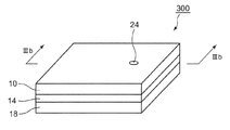
- FIG. 3A is a perspective view showing a multilayer substrate 300 according to the third embodiment of the present invention.
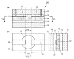
- FIG. 3B is a cross-sectional view showing a IIIb-IIIb cross section of FIG. 3A.
- FIG. 4A is a perspective view showing a multilayer substrate 400 according to the fourth embodiment of the present invention.
- FIG. 4B is a cross-sectional view showing a cross section IVb-IVb of FIG. 4A.
- FIG. 5 is a diagram illustrating the current cross-sectional area S1 and the inter-electrode distance D1 in the multilayer substrate 100 according to the first embodiment of the present invention.
- FIG. 6 is a diagram for explaining the current cross-sectional area S2 and the inter-electrode distance D2 in the multilayer substrate 200 according to the second embodiment of the present invention.
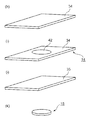
- FIG. 7A is a diagram illustrating a method for manufacturing the multilayer substrate 100.
- FIG. 7B is a diagram illustrating a method for manufacturing the multilayer substrate 100.
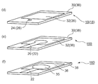
- FIG. 7C is a diagram illustrating a method for manufacturing the multilayer substrate 100.
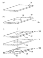
- FIG. 7D is a diagram illustrating a method for manufacturing the multilayer substrate 100.
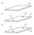
- FIG. 8A is a diagram illustrating a method for manufacturing the multilayer substrate 200.
- FIG. 8B is a diagram illustrating a method for manufacturing the multilayer substrate 200.
- FIG. 8C is a diagram illustrating a method for manufacturing the multilayer substrate 200.
- FIG. 8D is a diagram illustrating a method for manufacturing the multilayer substrate 200.
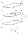
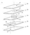
- FIG. 9A is a diagram illustrating a method for manufacturing the multilayer substrate 300.
- FIG. 9B is a diagram illustrating a method for manufacturing the multilayer substrate 300.
- FIG. 9C is a diagram illustrating a method for manufacturing the multilayer substrate 300.
- FIG. 10A is a diagram illustrating a method for manufacturing the multilayer substrate 400.
- FIG. 10B is a diagram illustrating a method for manufacturing the multilayer substrate 400.
- FIG. 10C is a diagram illustrating a method for manufacturing the multilayer substrate 400.
- FIG. 10D is a diagram illustrating a method for manufacturing the multilayer substrate 400.
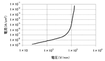
- 11 shows a sample No. in the example. It is a figure which shows the measurement result which measured the varistor characteristic of 10.
- 12 shows a sample No. of Example. It is a figure which shows the cross-sectional photograph of 32.
- a varistor layer and a dielectric layer (hereinafter sometimes referred to as a first dielectric layer and a second dielectric layer)
- a diffusion preventing layer containing Zn—Si oxide and Bi—Si oxide (hereinafter sometimes referred to as a first diffusion preventing layer and a second diffusion preventing layer) is disposed between It was found that the non-linear constant of the varistor layer in the multilayer board with a built-in varistor later can be similarly high as compared with the varistor layer alone.
- FIG. 1A is a perspective view showing the overall configuration of the varistor-embedded multilayer substrate 100 according to the first embodiment
- FIG. 1B is a cross-sectional view showing a cross section taken along line Ib-Ib of FIG. 1A
- a multilayer substrate 100 includes a varistor layer-containing insulator layer 14, a first diffusion prevention layer 12 provided in contact with the upper surface of the varistor layer-containing insulator layer 14, and a first diffusion prevention layer.
- the first dielectric layer 10 provided in contact with the upper surface of the second dielectric layer 12, the second diffusion prevention layer 16 provided in contact with the lower surface of the varistor layer-containing insulator layer 14, and the lower surface of the second diffusion prevention layer 16 And a second dielectric layer 18 provided in contact with the second dielectric layer 18. That is, in order from the bottom (in the embodiment shown in FIG. 1A, in order from the bottom), the second dielectric layer 18, the second diffusion prevention layer 16, the varistor layer-containing insulator layer 14, and the first diffusion prevention layer 12 The first dielectric layer 10 is laminated. As shown in FIG.
- the varistor layer-containing insulator layer 14 in the varistor-embedded multilayer substrate 100 according to the first embodiment, includes the varistor layer 15 and the insulator layer, and penetrates through the insulator layer. A varistor layer 15 is disposed inside the hole.
- the varistor layer-containing insulator layer 14 is not limited to this form.
- the varistor layer-containing insulator layer 14 may include only the varistor layer 15 without including an insulator layer.
- Internal electrodes 20 and 22 are disposed on the upper and lower surfaces of the varistor layer 15, respectively.
- the first internal electrode 20 disposed on the top surface of the varistor layer 15 is connected to the first through electrode 24 that penetrates the first dielectric layer 10 and the first diffusion prevention layer 12. Thereby, the part through which the 1st penetration electrode 24 was exposed from the upper surface of the 1st dielectric material layer 10, and the varistor layer 15 can be electrically connected.
- the second internal electrode 22 disposed on the lower surface of the varistor layer 15 is connected to a second through electrode 26 that penetrates the second diffusion prevention layer 16 and the second dielectric layer 18. Thereby, the portion where the second through electrode 26 is exposed from the lower surface of the second dielectric layer 18 and the varistor layer 15 can be electrically connected.
- the first internal electrode and the second internal electrode are counter electrodes facing each other, and the varistor layer 15 is disposed therebetween.
- the varistors pass through the through electrodes 24 and 26 and the internal electrodes 20 and 22.
- a current flows through the layer 15, and a current hardly flows through a device to be protected such as a semiconductor chip, so that these devices can be protected.
- the electrical wiring formed by the electrodes is almost in the insulating layer. Therefore, it is possible to realize a multilayer substrate that takes advantage of the excellent transmission characteristics of the insulating layer.
- the first through electrode 24 is disposed inside the multilayer substrate 100 so as to penetrate the first dielectric layer 10 and the first diffusion prevention layer 12. It is not limited to this configuration. That is, the first through electrode 24 may be in any form as long as it can be electrically connected to the first internal electrode 20 and the varistor layer 15 and the external power source can be electrically connected. Instead of the through electrode 24, an electrode disposed on the side surface of the multilayer substrate 100 may be used. Similarly, the second through electrode 26 may be in any form as long as it can be electrically connected to the second internal electrode 22 and the varistor layer 15 and the external power source can be electrically connected. Instead of the two through-electrodes 26, electrodes arranged on the side surfaces of the multilayer substrate 100 may be used.
- the varistor layer 15 is disposed such that at least a part of the upper surface thereof is in contact with the lower surface of the first diffusion prevention layer 12. Similarly, the varistor layer 15 is disposed such that at least a part of the lower surface thereof is in contact with the upper surface of the second diffusion prevention layer 16. As will be described later, the first diffusion prevention layer 12 and the second diffusion prevention layer 16 are formed so that the bismuth (Bi) contained in the varistor layer 15 is the first dielectric layer 10 and the second diffusion layer 15 during the sintering in the production of the multilayer substrate 100. It is disposed as a diffusion preventing layer for preventing diffusion to the dielectric layer 18.
- the varistor layer 15 in the multilayer substrate 100 can have a non-linear constant that is as high as that of a single varistor.
- the varistor layer 15 of the multilayer substrate 100 according to the present invention has a main phase of ZnO, and a Zn—Bi—Si—M oxide (at the grain boundary or grain boundary triple point of the ZnO crystal grain).
- M is one or more elements of Co, Mn, and Cr) and / or Zn-Si-M oxide (M is one or more elements of Co, Mn, and Cr).
- the varistor layer 15 having the following composition can have sufficient varistor characteristics even when baked at a low temperature of 850 ° C. to 1000 ° C.
- the composition of the varistor layer will be described below.
- ABC oxide when described as an ABC oxide (A to C are element symbols), it may be one composite oxide containing A, B, and C, or A, B And oxides containing a plurality of oxides containing one or more elements of C and C (for example, A oxide, B oxide, and C oxide).
- the varistor layer 15 has an overall composition including ZnO as the main phase and Zn—Bi—Si—M oxide and / or Zn—Si—M oxide portion present at the grain boundaries.
- Zn is contained at 90.0 mol% or more
- Si is contained at 0.01 to 2.0 mol%
- Bi is contained at 0.3 to 4.0 mol%
- Cr, 0.1 to 4.0 mol% of Mn, and 0.1 to 2.0 mol% of Co are included.
- “the whole metal element is 100 mol%” in defining the composition means “the whole metal element containing a semimetal such as Si, B and Sb is 100 mol%”.
- the metal element conversion means the content of the metal “when the entire metal element is 100 mol%”.
- the varistor layer 15 includes ZnO as a main phase and Zn—Bi—Si—M oxide and / or Zn—Si—M oxide present at grain boundaries.
- the total composition including the part of the product includes 0.01 to 2.0 mol% of Si and 0.3 to 4.0 mol% of Bi, and 0.1 to 2. It contains at least one selected from 0 mol% Cr, 0.1 to 4.0 mol% Mn, and 0.1 to 2.0 mol% Co, with the balance being Zn, unavoidable impurities, and will be described later It may contain other elements.
- the composition of the Zn-Bi—Si—M oxide is such that Zn is 10 mol% or more, Si is 0.5 to 8.0 mol%, Bi when the entire metal element is 100 mol%. 30.0-70.0 mol%, selected from 0.1-8.0 mol% Cr, 0.2-4.0 mol% Mn, and 0.2-3.0 mol% Co Contains one or more.
- the balance may be only inevitable impurities, but may further contain other elements.
- the composition of the Zn—Si—M oxide is such that Zn is 50 mol% or more, Si is 28.0 to 40.0 mol%, and Bi is 1 when the entire metal element is 100 mol%. 0.0 mol% or less, including at least one selected from 0 to 1.0 mol% of Cr, 0 to 1.5 mol% of Mn, and 0 to 2.4 mol% of Co.
- the remaining part of the Zn—Si—M oxide may be inevitable impurities, but may further contain other elements.
- the varistor layer 15 according to the present invention contains each element so as to have the above-described composition
- Bi and Si contained in the varistor layer 15 are obtained when the multilayer substrate 100 according to the present invention is fired.
- a Zn—Bi—Si—M oxide is formed.
- diffusion of Bi in the varistor layer to the outside of the varistor layer can be suppressed, and the varistor-embedded multilayer substrate 100 according to the present invention after firing has a high non-linear constant equivalent to that of a single varistor layer. Can do.
- the varistor layer 15 according to the present invention preferably has a Si composition in the range of 0.1 to 2.0 mol%.
- the varistor-embedded multilayer substrate 100 according to the present invention after firing can have a higher nonlinear constant.
- the varistor layer 15 preferably contains antimony (Sb), rare earth elements, and tin (Sn) in an impurity level or less.
- “below the impurity level” means containing only an amount recognized as zero or an impurity level or lower. Below, the amount recognized as an impurity level is described about each of antimony (Sb), rare earth elements, and tin (Sn).
- Antimony (Sb) The general content of antimony (Sb) recognized as the impurity level is, for example, 0.01 mol% or less, preferably 0.005 mol% or less when the entire metal element is 100 mol%. For practical measurement, for example, if it is below the detection limit (100 ppm by mass ratio) of an ICP (inductively coupled plasma) wet analyzer, the condition of 0.01 mol% or less is satisfied.
- ICP inductively coupled plasma
- the general content of the rare earth element recognized as the impurity level is, for example, about 0.01 mol% or less for each rare earth element when the entire metal element is 100 mol%, and the total rare earth element is 0 .05 mol% or less. Preferably, it is 0.005 mol% or less for each of the rare earth elements, and the total rare earth elements is 0.025 mol% or less. For practical measurement, for example, if it is below the detection limit (100 ppm by mass ratio) of an ICP (inductively coupled plasma) wet analyzer, the condition of 0.01 mol% or less is satisfied.
- ICP inductively coupled plasma
- rare earth element is yttrium (Y), lanthanum (La), cerium (Ce), praseodymium (Pr), neodymium (Nd), promethium (Pm), samarium (Sm), europium (Eu). , Gadolinium (Gd), terbium (Tb), dysprosium (Dy), holmium (Ho), erbium (Er), thulium (Tm), ytterbium (Yb) and lutetium (Lu). That is, “rare earth element” in this specification does not include scandium (Sc).
- Tin (Sn) The general content of tin (Sn) recognized as the impurity level is, for example, 0.01 mol% or less, preferably 0.005 mol% or less when the entire metal element is 100 mol%. For practical measurement, for example, if it is below the detection limit (100 ppm by mass ratio) of an ICP (inductively coupled plasma) wet analyzer, the condition of 0.01 mol% or less is satisfied.
- ICP inductively coupled plasma
- the varistor layer 15 according to the present invention may contain Zn, unavoidable impurities, and other elements as the balance.
- An example of the level of such inevitable impurities is 0.03 mol% or less per one kind of element, and 0.1 mol% or less of the inevitable impurities as a whole.
- the “inevitable impurities” usually means impurities that are unintentionally contained during the manufacturing process and handling. However, even if it is intentionally added, if the content is not more than the above-mentioned “impurity level”, the technical effect due to the addition cannot be sufficiently obtained.
- “inevitable impurities” means that the content is below the above “impurity level” regardless of whether it is intentionally added or unintentionally contained. To do. Therefore, in the present invention, as described above, since the contents of antimony (Sb), rare earth element, and tin (Sn) are not more than the impurity level, antimony (Sb), rare earth element, and tin (Sn) are inevitable. It is included in "impurity”.
- one or more arbitrary elements other than antimony (Sb), rare earth elements and tin (Sn) may be contained in order to obtain desired varistor characteristics.
- Such elements may be contained in a total of, for example, 10 mol% or less, preferably 5 mol% or less. If it is about this level, it is possible to ensure sufficient varistor characteristics.
- the varistor layer 15 of the present invention may contain boron oxide such as B 2 O 5 , for example.
- boron oxide is contained in an amount of 0.1 to 4.0 mol%, preferably 0.1 to 2.0 mol% in terms of boron (B).
- Boron oxide (boron) has the effect of improving sinterability. If the content of boron oxide is less than 0.1 mol% in terms of boron, this effect cannot be obtained sufficiently, and if it exceeds 4.0 mol%, there is a problem in that it segregates by forming a glass component together with other additives. In addition, if the preferable range is 0.1 to 2.0 mol%, this effect can be obtained more sufficiently.
- the varistor layer 15 of the present invention may contain scandium oxide such as Sc 2 O 3 , for example.
- scandium oxide is contained in an amount of 0.1 to 2.0 mol%, preferably 0.4 to 0.7 mol% in terms of scandium (Sc).
- Scandium oxide (scandium) has an effect of improving sinterability. If the content of scandium oxide is less than 0.1 mol% in terms of scandium, this effect cannot be sufficiently obtained, and if it exceeds 2.0 mol%, there is a problem that densification becomes difficult and segregation increases. Further, if the preferred range is 0.4 to 0.7 mol%, this effect can be obtained more sufficiently.
- Varistor layer 15 of barium oxide present invention may contain barium oxide such as Ba 2 O.
- barium oxide is contained in an amount of 0.1 to 2.0 mol%, preferably 0.2 to 1.5 mol% in terms of barium (Ba).
- Barium oxide (barium) contributes to forming a suitable grain boundary by segregating at the grain boundary. If the content of barium oxide is less than 0.1 mol% in terms of barium, this effect cannot be sufficiently obtained, and if it exceeds 2.0 mol%, there is a problem that sintering is inhibited and barium oxide is segregated. In addition, if the preferable range is 0.2 to 1.5 mol%, this effect can be more sufficiently obtained.
- the varistor layer 15 of the present invention may further include one or more selected from the group consisting of zirconium oxide and tungsten oxide, if necessary. These oxides have the effect of improving the nonlinear constant.
- zirconium oxide is contained, the above-mentioned effects can be obtained by containing zirconium oxide in an amount of 0.1 to 2.0 mol% (preferably 0.2 to 1.5 mol%) in terms of zirconium (Zr).
- tungsten oxide is contained, the above-described effects can be obtained by containing tungsten oxide in an amount of 0.1 to 2.0 mol% (preferably 0.2 to 1.5 mol%) in terms of tungsten (W).
- the varistor layer 15 includes ZnO as a main phase and Zn—Bi—Si—M oxide and / or Zn—Si—M oxide present at grain boundaries.
- the composition of Si is 0.01 to 0.3 mol%, preferably 0.01 to 0.1 mol%, more preferably May be 0.01 to 0.05 mol%.
- the multilayer substrate 100 according to the present invention when the multilayer substrate 100 according to the present invention is obtained by firing, Bi contained in the varistor layer 15 reacts with Si, A Zn—Bi—Si—M oxide is formed. As a result, the diffusion of Bi in the varistor layer to the outside of the varistor layer can be suppressed. As a result, the multilayer substrate 100 with a built-in varistor according to the present invention after firing has the same high nonlinearity as that of a single varistor layer. Can have a constant.
- the insulating performance of the varistor-embedded multilayer substrate 100 according to the present invention after firing is further improved, and it is equivalent to the case of a single varistor layer. It can have a high nonlinear constant.
- the first and second diffusion-preventing layers 12 and 16 according to the present invention include a Zn—Si oxide mainly composed of Zn 2 SiO 4 and a Bi—Si oxide. Yes.
- the total composition including the Zn—Si oxide portion and the Bi—Si oxide portion is Zn when the entire metal element is 100 mol%. 30 mol% or more, Si 26.6 to 55.0 mol%, and Bi 1.5 to 35.0 mol%.
- the overall composition including the Zn—Si oxide portion and the Bi—Si oxide portion is: Si may be included in an amount of 26.6 to 55.0 mol%, Bi may be included in an amount of 1.5 to 35.0 mol%, and the balance may include Zn, inevitable impurities, and other elements.
- the other elements that may be included in the first and second diffusion preventing layers 12 and 16 are Al, Ag, Cr, Mn, Co, and the like. In the present invention, these elements are derived from the adjacent varistor layer 15, dielectric layers 10, 18 and / or Ag electrode when the multilayer substrate 100 is co-fired.
- the first and second diffusion preventing layers 12 and 16 are made of 0 to 2.0 mol% Al, 0 to 2.0 mol% Ag, 0 to 1.0 mol% Cr, 0 to 1.0 mol Mn. Even when 0 mol% and Co are included in the range of 0 to 1.0 mol%, the effect according to the present invention can be obtained.
- the composition of the Zn—Si oxide containing Zn 2 SiO 4 as a main component is such that Zn is 60 mol% or more when the entire metal element is 100 mol%.
- Si is contained in an amount of 30.0 to 40.0 mol%
- Bi is contained in an amount of 0 to 2.0 mol%.
- the remainder of the Zn—Si oxide may be inevitable impurities only, but may contain other elements described above as long as Zn is 60 mol% or more.
- Zn 2 SiO 4 is the main component of “Zn—Si oxide” means that “Zn 2 SiO 4 ” is 50% or more by volume in the “Zn—Si oxide”.
- the composition of the Bi—Si oxide is such that Si is 30.0 to 70.0 mol% and Bi is 5 when the entire metal element is 100 mol%. 0.0 to 30.0 mol%.
- the remainder of the Bi—Si oxide may be inevitable impurities only, but may contain other elements described above as long as it contains 5.0 to 30.0 mol% of Bi.
- the first and second diffusion preventing layers 12 can be formed when the multilayer substrate 100 according to the present invention is fired. , 16 a dense Bi-Si oxide structure is formed. Thereby, when the multilayer substrate 100 is baked, the diffusion of Bi contained in the varistor layer into the insulating layer can be suppressed. Further, by providing the first and second diffusion preventing layers 12 and 16 containing a large amount of Bi between the varistor layer 15 and the first and second dielectric layers 10 and 18, other layers adjacent to the varistor layer 15 are provided. The gradient of the Bi concentration between the varistor layer 15 and the varistor layer 15 can be slowed down. As a result, the varistor-embedded multilayer substrate 100 according to the present invention after firing can have a high nonlinear constant equivalent to that of a single varistor layer.
- compositions of the first diffusion preventing layer 12 and the second diffusion preventing layer 16 according to the present invention may be different compositions or the same composition as long as they are within the composition range described above. If the first diffusion prevention layer 12 and the second diffusion prevention layer 16 have the same composition, raw materials before sintering of the first diffusion prevention layer 12 and the second diffusion prevention layer 16 can be obtained by the same manufacturing process. Therefore, the manufacturing process as a whole can be made efficient.
- the first and second dielectric layers 10 and 18 according to the present invention have voids of less than 5% in area ratio, electric resistivity of 10 10 ⁇ ⁇ cm or more, and a relative dielectric constant of 6 to Nine.
- the void area ratio is less than 5%, the fracture strength of the substrate is improved.
- the electrical resistivity is 10 10 ⁇ ⁇ cm or more, there is an effect of excellent insulation.
- the relative dielectric constant is 6 to 9, there is an effect that the parasitic capacitance is reduced and excellent in high-speed transmission.
- the first and second dielectric layers 10 and 18 are ceramic compositions containing an Al—Si—Sr oxide as a main component and containing SrAl 2 Si 2 O 8 , Al 2 O 3 and TiO 2. Also good. By having such a composition, the first and second dielectric layers 10 and 18 can be fired at a temperature of 1000 ° C. or lower, for example, 850 ° C. to 950 ° C., and have excellent dielectric properties. Can do. “Al—Si—Sr oxide” as a main component means that “Al—Si—Sr oxide” is 50% or more by volume in the dielectric layer.
- first and second dielectric layers 10 and 18 having the above-described structure have Al content of 23.6 to 63.5 mol%, Si content of 100 mol% of the entire metal element including Si. 24.2 to 60.0 mol%, Sr 5.1 to 26.8 mol%, Ti 0.1 to 2.8 mol%, Bi 0.1 to 0.7 mol%, Na 0.1 to 3 .4 mol%, K 0-1.2 mol%, Co 0-0.5 mol%, Cu 0.1-0.7 mol%, Mn 0.1-0.6 mol%, Ag 0.1- 2.0 mol% and 0.4 to 1.7 mol% Zr are contained.
- the portion excluding the varistor layer 15 may be a dielectric, and the composition and structure of the dielectric are the same as those of the first and second dielectric layers 10 and 18. Also good.
- compositions of the first dielectric layer 10 and the second dielectric layer 18 according to the present invention may be different compositions or the same composition as long as they are within the composition range described above. If the first dielectric layer 10 and the second dielectric layer 18 have the same composition, raw materials before sintering the first dielectric layer 10 and the second dielectric layer 18 can be obtained by the same manufacturing process. Therefore, the manufacturing process as a whole can be made efficient.
- the composition of the varistor layer, the diffusion prevention layer and the dielectric layer of the multilayer substrate according to the present invention can be analyzed by the following procedure.
- a multilayer board with a built-in varistor obtained by simultaneously firing a dielectric layer, a diffusion prevention layer, and a varistor layer is cut using an outer peripheral cutting machine, and the resulting cut piece is filled with resin.
- a cross section polisher (ion polisher) is used to polish a cross section aiming at a portion where a cross sectional observation image of the structure shown in FIG. 1B is obtained.
- the polished surface is observed with an FE-SEM, and the portion to be measured is aimed at the point and analyzed by EDX (energy dispersive X-ray spectroscopy).
- the analysis may be performed using an X-ray spectrum obtained by irradiating a rectangular area of 10 ⁇ m ⁇ 10 ⁇ m or more with an electron beam.
- an analysis may be performed using an X-ray spectrum obtained by irradiation with a beam diameter of 1 ⁇ m or less.
- the whole metal element is converted to 100 mol%.
- the contained crystal structure is determined by X-ray diffraction.
- the Zn—Bi—Si—M oxide is observed with a bright contrast and the Zn—Si—M oxide is observed with a dark contrast when observed with an SEM.
- the Bi—Si oxide is easily distinguished because it looks brighter than the Zn—Si oxide.
- the size of the Bi—Si oxide is about 1 ⁇ m, the characteristic X-rays of Zn derived from the Zn—Si oxide present in the periphery are detected at the time of analysis, so that the Bi—Si—Zn oxide is not detected. It looks like.
- the SEM-EDX method is applied to the Bi-containing region, provisionally defined as Bi-Si oxide, Zn content is regarded as 0 mol%, and elements other than Zn and O are converted as 100 mol%. evaluate. That the Zn—Si oxide is Zn 2 SiO 4 is estimated from the ratio of the analytical values.
- FIG. 2A is a perspective view showing a multilayer substrate 200 with a built-in varistor according to the second embodiment
- FIG. 2B is a cross-sectional view showing a IIb-IIb cross section of FIG. 2A.
- both the first internal electrode 20 and the second internal electrode 22 are the same main surface of the two main surfaces of the varistor layer 15. It is different from the multilayer substrate 100 with a built-in varistor 100 according to the first embodiment in that it is disposed on the upper surface of the varistor layer 15 in FIG. 2B. With such a configuration, an effect that the thickness of the varistor element can be reduced can be obtained.
- the integrated circuit connected to the multilayer substrate 200 is affected by noise or the like.
- an abnormally high voltage high current
- a current flows through the varistor layer 15 via the first and second through electrodes 24, 26 and the first and second internal electrodes 20, 22, and the semiconductor chip or the like Almost no current flows through the devices to be protected, so that these devices can be protected.
- the first and second diffusion prevention layers 12 and 16 are disposed between the varistor layer 15 and the first and second dielectric layers 10 and 18, respectively.
- the diffusion of Bi from the varistor layer 15 to other layers due to sintering is suppressed, and the multilayer substrate 200 with a built-in varistor can have a high nonlinear constant.
- FIG. 3A is a perspective view showing a multilayer substrate 300 with a built-in varistor according to the third embodiment
- FIG. 3B is a cross-sectional view showing a IIIb-IIIb cross section of FIG. 3A.
- the multilayer substrate 300 with a built-in varistor according to the third embodiment is provided so that the first diffusion prevention layer 12 is in contact with the first dielectric layer 10 not only on the top surface but also on the top surface and side surfaces.
- the second diffusion prevention layer 16 is provided so as to be in contact with the second dielectric layer 18 not only on the lower surface but also on the lower surface and the side surface.
- the built-in varistor according to the first embodiment is provided. Different from the multilayer substrate 100.
- the first through electrode 24 does not penetrate the first diffusion prevention layer 12 and penetrates only the first dielectric layer 10.
- the second through electrode 26 is different from the varistor built-in multilayer substrate 100 according to the first embodiment in that the second through electrode 26 does not penetrate the second diffusion prevention layer 16 and penetrates only the second dielectric layer 18. .
- the first and second through electrodes 24 and 26 and the first and second internal electrodes 20. , 22 current flows through the varistor layer 15, and almost no current flows through a device to be protected such as a semiconductor chip, so that these devices can be protected.
- the first and second diffusion prevention layers 12 and 16 are disposed between the varistor layer 15 and the first and second dielectric layers 10 and 18, respectively.
- the diffusion of Bi from the varistor layer 15 to other layers is suppressed by sintering, and the multilayer substrate 300 with a built-in varistor can have a high nonlinear constant.
- FIG. 4A is a perspective view showing a multilayer substrate 400 with a built-in varistor according to the fourth embodiment
- FIG. 4B is a cross-sectional view showing a IVb-IVb cross section of FIG. 4A.
- both the first internal electrode 20 and the second internal electrode 22 are the same main surface of the two main surfaces of the varistor layer 15. Is different from the multilayer board 300 with a built-in varistor according to the third embodiment. With such a configuration, an effect that the thickness of the varistor element can be reduced can be obtained.
- the integrated circuit connected to the multilayer substrate 400 is affected by noise or the like.
- an abnormally high voltage high current
- a current flows through the varistor layer 15 via the first and second through electrodes 24, 26 and the first and second internal electrodes 20, 22, and the semiconductor chip or the like Almost no current flows through the devices to be protected, so that these devices can be protected.
- the first and second diffusion prevention layers 12 and 16 are disposed between the varistor layer 15 and the first and second dielectric layers 10 and 18, respectively.
- Varistor characteristics As described above, the multilayer substrate with a built-in varistor of the present invention having the above-described composition has excellent varistor characteristics equivalent to those of a single varistor layer. Accordingly, the varistor characteristics of the multilayer substrate with built-in varistor of the present invention will be described below. Current-voltage characteristics, insulation resistance, and nonlinear resistance are known as main varistor characteristics.
- FIGS. 5A and 5B are diagrams illustrating the current cross-sectional area S1 and the interelectrode distance D1 in the multilayer substrate 100 according to the first embodiment of the present invention.
- 5A is a cross-sectional view showing the Ib-Ib cross section of FIG. 1A, and FIG.
- FIG. 5B is a cross-sectional view showing the Vb-Vb cross section of FIG. 5A.
- the first diffusion prevention layer 12 is omitted and the second internal electrode 22 is indicated by a dotted line.
- the current cross-sectional area is It is an area (S1 shown in FIG. 5B) that overlaps the first and second internal electrodes when viewed from the stacking direction of the multilayer substrate, and the distance between the electrodes is the first internal electrode 20 and the second internal electrode. 22 is the shortest distance (D1 shown in FIG. 5A).
- FIG. 5A and 5B exemplarily illustrate how to define the current cross-sectional area S1 and the interelectrode distance D1 in the multilayer substrate 100 according to the first embodiment.
- the current cross-sectional area S1 and the inter-electrode distance D1 are the same as described above in the case of a multilayer substrate provided with a plurality of electrodes facing different main surfaces of the varistor layer. Can be specified.
- the same definition can be applied to the multilayer substrate 300 according to the third embodiment.
- FIGS. 6A to 6C are diagrams for explaining the current cross-sectional area S2 and the inter-electrode distance D2 in the multilayer substrate 200 according to the second embodiment of the present invention.
- 6A is a cross-sectional view showing a IIb-IIb cross section of FIG. 2A
- FIG. 6B is a cross-sectional view showing a VIb-VIb cross section of FIG. 6A
- FIG. 6C is a cross-sectional view showing a VIc-VIc cross section of FIG.
- the first diffusion prevention layer 12 is omitted for easy explanation. As shown in FIG.
- the current cross-sectional area is the thickness of the varistor layer 15. Is the area obtained by multiplying the width of the first internal electrode by the width of the first internal electrode (S2 shown in FIG. 6C), and the interelectrode distance is the distance between the first internal electrode 20 and the second internal electrode 22
- 6A, 6 ⁇ / b> B, and 6 ⁇ / b> C illustrate how to define the current cross-sectional area S ⁇ b> 2 and the interelectrode distance D ⁇ b> 2 in the multilayer substrate 200 according to the second embodiment. However, this rule is not limited to the second embodiment.
- the current cross-sectional area S2 and the interelectrode distance D2 are defined in the same manner as described above. can do.
- the same definition can be applied to the multilayer substrate 400 according to the fourth embodiment.
- the insulation resistivity ( ⁇ ⁇ cm) means a resistivity when a terminal voltage of 25 V / mm is applied to a varistor element having a current cross-sectional area of 1 cm 2 .
- the voltage (V / mm) may be divided by the current value (A / cm 2 ) and multiplied by 10 as an equivalent value.
- the insulation resistivity is low, a large amount of current flows and leak current is generated. For this reason, it is considered that the element has an insulation resistance of 10 M ⁇ or more. And in order to achieve this 10 M ⁇ reliably, when it has a higher resistivity, the freedom degree of design is high and preferable.
- Nonlinear constant When the current-voltage characteristic is expressed with a logarithmic axis as a nonlinear constant, the slope of the tangent at the point where the current value becomes 1 mA / cm 2 is defined as the nonlinear constant.
- the calculation method of the slope of the tangent line includes two measurement points in the range of V 1 +0.05 V 1 with respect to the voltage value V 1 (V / mm) at which the current value is 1 mA / cm 2, and V 1 ⁇ 0
- the least square method was applied to a total of four measurement points in a range of .05V 1 and the obtained gradient was defined as the tangential gradient.
- Many of the sintered bodies for zinc oxide varistors containing rare earth elements have a non-linear constant of 20 or more.
- a nonlinear constant of, for example, 20 or more, or 25 or more can be obtained.
- the varistor-embedded multilayer substrate of the present invention has a reduced varistor layer porosity when the Si composition of the varistor layer is 0.01 to 0.3 mol%.
- the insulating performance of the varistor built-in multilayer substrate can be further improved.
- the porosity of the varistor layer is 20% or less, it can be said that the porosity is reduced and the insulation performance is further improved. Therefore, the porosity of the varistor layer of the multilayer substrate with a built-in varistor of the present invention will be described below.
- the porosity of the varistor layer is the percentage of the volume of pores per unit volume of the varistor layer expressed as a percentage.
- the porosity of the varistor layer is determined as follows.
- the varistor layer of the multilayer substrate with a built-in varistor to be measured is cut by machining, the cross section is polished, and then five fields of view for measuring the porosity are randomly selected from the polished surface and observed with a scanning electron microscope. .
- the area ratio of the hole portion in the field of view is calculated.
- the calculation method binarizes the vacancies and other portions in the observed image, and obtains the area ratio of the vacancies.
- an observation image is printed on a paper surface, and only a hole portion is blacked out, read by a scanner, and obtained by image processing using commercially available image processing software.
- Scandium manufactured by OLYMPUS
- OLYMPUS optical microparticle scanner
- the average value of the area ratios of the hole portions in the five visual fields obtained in this way is defined as the porosity (%) of the varistor layer.
- the production method includes (1) a step of producing a varistor layer powder sheet, and (2) a diffusion prevention layer powder sheet. A step of producing, (3) a step of producing a dielectric layer powder sheet, and (4) a step of laminating and baking the varistor layer powder sheet, the diffusion prevention layer powder sheet and the dielectric layer powder sheet.
- a mixed raw material having the following composition.
- the composition of the mixed raw material includes at least 0.3 to 4.0 mol% of bismuth oxide in terms of bismuth and 0.01 to 2.0 mol% of silicon oxide in terms of silicon, and 0.1 to 2.5 mol in terms of cobalt. 1% or more selected from cobalt oxide, 0.1 to 2.5 mol% chromium oxide in terms of chromium, and 0.1 to 5.0 mol% manganese oxide in terms of manganese, with the remainder being zinc oxide.
- the raw material composition of the varistor layer is set in anticipation of element diffusion from the varistor layer to the diffusion prevention layer or dielectric layer and element diffusion from the diffusion prevention layer or dielectric layer to the varistor layer.
- the composition of the mixed raw material is used to promote mixing or to hold the mixed mixed powder in a slurry state, and most of it evaporates in the firing step.
- ethanol and PVB Polyvinyl butyral
- a plasticizer such as dioctyl phthalate used for maintaining the shape during sheet molding are not included.
- the composition of the mixed raw material is used to make the mixed raw material into a desired shape such as a sheet, and most of it evaporates in the firing process, organic solvent, plasticizer, binder And no vehicles obtained from these.
- the mixed raw material can be obtained, for example, by weighing the raw materials of the oxide (including the above-mentioned additives that are added as necessary) so as to have the above composition, and then mixing these raw materials.
- the mixed raw materials are weighed so as to have the above composition in the state of a compound of Si 4 Bi 3 Si 3 O 12 and the remaining elements in the state of raw materials of the respective oxides, and then mixed together. May be obtained.
- the particle size is about 3 to 10 ⁇ m.
- Zn 2 SiO 4 may form in the varistor layer.
- the multilayer board with a built-in varistor after firing can have the excellent varistor characteristics described above, but the grain size of Zn 2 SiO 4 can be reduced. By making it smaller, the varistor layer after firing can be densified, and the insulation performance of the varistor-embedded multilayer substrate can be further improved. As described above, the present inventors have found that by adding Si in the state of Bi 4 Si 3 O 12 compound, the particle size of Zn 2 SiO 4 produced during firing can be suppressed to about 1 ⁇ m or less.
- the varistor layer can be further densified, and the insulating performance of the varistor-embedded multilayer substrate after firing can be further improved.
- the addition of Si in the form of compounds of Bi 4 Si 3 O 12 since Bi is also added at a ratio of Bi 4 Si 3 O 12, with respect to the Bi, the Bi 4 Si 3 O 12 from the target value of the composition
- An amount obtained by subtracting the amount of Bi supplied may be added in the state of Bi oxide (Bi 2 O 3 ).
- the composition of Si is 0.01 to 0.3 mol%, preferably 0.01 to 0.1 mol%, more preferably 0.01 to 0.05 mol%, of the total composition of the varistor layer.
- the bismuth-silicon oxide compound (Bi 4 Si 3 O 12 ) may be prepared as follows. A mixed raw material (mixed powder) of bismuth oxide (Bi 2 O 3 ) and silicon oxide (SiO 2 ) is prepared. Bismuth oxide and silicon oxide are weighed and mixed so that the composition of the mixed raw material is Bi 4 Si 3 O 12 . Mixing may be performed for 20 hours by a ball mill of an aqueous solvent. After mixing is completed, the slurry is recovered and dried to obtain a mixed raw material. By heat-treating the obtained mixed powder at 700 to 800 ° C. in the atmosphere, a compound having Bi 4 Si 3 O 12 as a main phase can be obtained.
- the powder obtained by the heat treatment may be pulverized in advance with a ball mill to reduce the particle size.
- An example of the mixing method is to use a ball mill.
- a dispersion medium such as ethanol and a raw material weighed together with balls such as zirconia balls may be put into a ball mill container and ball mill mixing may be performed to obtain a mixed raw material.
- the obtained mixed raw material is dispersed in an organic dispersion medium such as ethanol or an inorganic dispersion medium to obtain a slurry (slurry mixed raw material, paste).
- the obtained slurry is molded by a known sheet molding method, for example, a doctor blade method using a sheet molding machine to obtain a varistor layer powder sheet.
- composition formula (1) Zn 2 SiO 4 + xBi 2 O 3 + ySiO 2 (0.06 ⁇ x ⁇ 1.30, 0.50 ⁇ y ⁇ 2.00) (1)
- the above composition formula (1) is a target composition in the case of producing a diffusion prevention layer.
- the diffusion prevention layer composition after firing includes elements derived from varistor layers, dielectric layers, and Ag electrodes by diffusion from each layer.
- the composition may be different from the target composition by diffusing each element from the diffusion preventing layer into each layer.
- An example of the mixing method is to use a ball mill.
- a dispersion medium such as ethanol and a raw material weighed together with balls such as zirconia balls may be put into a ball mill container and ball mill mixing may be performed to obtain a mixed raw material.
- the obtained mixed powder of Zn 2 SiO 4 and SiO 2 is heat-treated (calcined) at 1100 ° C. to 1300 ° C. to obtain a calcined powder.
- Bismuth oxide is added to the calcined powder in the state of Bi 2 O 3 and mixed.
- a mixing method for example, a ball mill may be used.
- the mixed raw material obtained by mixing is dispersed in an organic dispersion medium such as ethanol or an inorganic dispersion medium to obtain a slurry (slurry mixed raw material, paste).
- PVB or the like is added to partially evaporate the solvent so that the viscosity of the slurry is about 3 Pa ⁇ s, and then a known sheet molding method, for example, a doctor using a sheet molding machine Molded by a blade method or the like to obtain a diffusion preventing layer powder sheet.
- Step of Producing Dielectric Layer Powder Sheet A method of producing a dielectric layer powder sheet that becomes a dielectric layer after sintering will be described.
- a mixed raw material (mixed powder) having the same composition as the dielectric layer to be obtained is prepared.
- the mixed raw materials are, for example, raw materials such as oxides such as aluminum oxide, silicon oxide, strontium carbonate, titanium oxide, bismuth oxide, copper oxide, manganese oxide, sodium carbonate, and potassium carbonate (added as necessary above) And a mixture of these raw materials after weighing so as to be the same as the composition of the dielectric layer to be obtained.
- the material composition of the dielectric layer may be set in anticipation of element diffusion from the dielectric layer to the diffusion prevention layer or varistor layer and element diffusion from the diffusion prevention layer or varistor layer to the dielectric layer.
- An example of the mixing method is to use a ball mill.
- a dispersion medium such as ethanol and a raw material weighed together with balls such as zirconia balls may be put into a ball mill container and ball mill mixing may be performed to obtain a mixed raw material.
- the obtained mixed raw material is calcined at 600 to 800 ° C., and the obtained calcined powder is dispersed in an organic dispersion medium or inorganic dispersion medium such as ethanol to obtain a slurry (slurry mixed raw material or paste).
- the obtained slurry is molded by a known sheet molding method, for example, a doctor blade method using a sheet molding machine to obtain a dielectric powder sheet.
- Multilayer substrate manufacturing process (multilayer substrate manufacturing process according to the first embodiment)
- the manufacturing process of a multilayer substrate is demonstrated.
- a manufacturing process of the varistor-embedded multilayer substrate 100 according to the first embodiment of the present invention will be described as an example.
- the manufacturing process can also be used in the manufacturing process of a varistor-embedded multilayer substrate according to another embodiment.
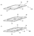
- FIGS. 7A to 7C are perspective views showing a method of manufacturing the pre-fired dielectric layer 10 (18).
- the pre-firing dielectric layer 10 (18) is produced.
- the dielectric material layer powder sheet 30 (38) used as a dielectric material layer by baking is prepared.
- the dielectric layer powder sheet 30 (38) for example, the one obtained by the method (3) described above is used.
- through holes 40 (41) are formed in the dielectric layer powder sheet 30 (38) by, for example, a laser.
- the through hole 40 (41) of the dielectric layer powder sheet 30 (38) is filled with a silver electrode paste and dried to dry the through electrode 24 (26 after firing).
- the electrode layer paste 24 (26) is formed.
- a screen printing method may be used for filling the through hole 40 (41) with the silver paste.
- the pre-firing dielectric layer 10 (18) can be obtained. Two of the same dielectric layers before firing, that is, the dielectric layer 10 before firing and the dielectric layer 18 before firing are produced.
- FIGS. 7D to 7G are perspective views showing a method for manufacturing the pre-firing diffusion prevention layer 12 (16).
- the diffusion prevention layer powder sheet 32 (36) used as a diffusion prevention layer by baking is prepared.
- the diffusion preventing layer powder sheet 32 (36) for example, the one obtained by the method (2) described above is used.
- the 1st through-hole 40 (41) is formed in the diffusion prevention layer powder sheet 32 (36) by a laser, for example.
- the through hole 40 (41) of the diffusion preventing layer powder sheet 32 (36) is filled with a silver electrode paste and dried to dry the through electrode 24 (26 after firing).
- the electrode layer paste 24 (26) is formed.
- a screen printing method may be used for filling the through hole 40 (41) with the silver paste.
- an electrode layer paste 20 (22) to be the internal electrode 20 (22) after firing is formed so as to overlap the electrode paste 24 (26).
- the electrode layer paste 20 (22) may use a screen printing method. Thereby, the diffusion preventing layer 12 (16) before firing can be obtained. Two of the same diffusion preventing layers before firing, that is, the diffusion preventing layer 12 before firing and the diffusion preventing layer 16 before firing are prepared.
- FIG. 7C are perspective views showing a method of manufacturing the pre-firing insulating layer 14.
- a dielectric layer powder sheet 34 to be an insulating layer is prepared by firing.
- the dielectric layer powder sheet 34 for example, the one obtained by the method (3) described above is used.
- varistor through-holes 42 are formed in the dielectric layer powder sheet 34 using, for example, a mold. Thereby, the insulating layer 14 before baking can be obtained.
- FIG. 7C are perspective views showing a method for manufacturing the pre-firing varistor layer 15.
- seat 35 used as a varistor layer by baking is prepared.
- the varistor layer powder sheet 35 for example, the one obtained by the method (1) described above is used.
- the varistor layer powder sheet 35 is punched out so as to have substantially the same shape as the varistor through-hole 42 of the insulating layer 14 before firing. Thereby, the pre-firing varistor layer 15 can be obtained.
- FIG. 7D (l) is a diagram showing a process of laminating each obtained layer.
- the pre-firing dielectric layer 18 and the electrode layer paste 22 are on the upper surface side, the second through hole 41 provided in the pre-firing diffusion prevention layer 16, and the first through-hole provided in the pre-firing dielectric layer 18.
- Pre-firing diffusion prevention layer 16 disposed so that two through-holes 41 overlap, and electrode layer paste 22 provided on the upper surface of pre-firing diffusion prevention layer 16 and varistor through-hole 42 are disposed so as to overlap.
- Pre-firing diffusion preventing layer 12 disposed so that 20 is the lower surface side and pre-firing varistor layer 15 and electrode layer paste 20 overlap, and first through-hole 40 provided in pre-firing diffusion preventing layer 12 and fired Pre-dielectric
- the obtained composite laminate is fired at a temperature range of 850 to 950 ° C. Thereby, the multilayer substrate 100 with a built-in varistor can be obtained.
- FIGS. 8A to 8C are perspective views showing a method of manufacturing the pre-fired dielectric layer 10 (18).
- the pre-firing dielectric layer 10 (18) is produced.
- the dielectric material layer powder sheet 30 (38) used as a dielectric material layer by baking is prepared.
- Two dielectric layer powder sheets, that is, a dielectric layer powder sheet 30 and a dielectric layer powder sheet 38 are prepared.
- the dielectric layer powder sheet 30 (38) for example, the one obtained by the method (3) described above is used.
- the dielectric layer powder sheet 38 is used as the pre-fired dielectric layer 18 as it is, and the pre-fired dielectric layer 10 is produced using the dielectric layer powder sheet 30 as follows. As shown in FIG.
- the first through hole 40 and the second through hole 41 are formed on the dielectric powder sheet 30 by, for example, a laser.
- the 1st through-hole 40 and the 2nd through-hole 41 are filled with a silver electrode paste, and are dried.
- electrode layer pastes 24 and 26 are formed, which become the first through electrode 24 and the second through electrode 26, respectively, after firing.
- a screen printing method may be used for filling the first through hole 40 and the second through hole 41 with the silver paste. Thereby, the pre-firing dielectric layer 10 can be obtained.
- FIG. 8B are perspective views showing a method for manufacturing the pre-firing diffusion prevention layer 12 (16).
- the diffusion prevention layer powder sheet 32 (36) used as a diffusion prevention layer by baking is prepared.
- Two powder sheets for the diffusion preventing layer are prepared, that is, a powder sheet 32 for the diffusion preventing layer and a powder sheet 36 for the diffusion preventing layer.
- the diffusion preventing layer powder sheet 32 (36) for example, the one obtained by the method (2) described above is used.
- the diffusion preventing layer powder sheet 36 is used as it is as the diffusion preventing layer 16 before firing, and the diffusion preventing layer 12 before firing is produced using the diffusion preventing layer powder sheet 32 as follows.
- the 1st through-hole 40 and the 2nd through-hole 41 are formed in the diffusion prevention layer powder sheet 32 with a laser, for example.
- the silver electrode paste is filled into the 1st through-hole 40 and the 2nd through-hole 41 of the diffusion prevention layer powder sheet 32, and it is made to dry.
- electrode layer pastes 24 and 26 to be the first through electrode 24 and the second through electrode 26 after firing are formed.
- a screen printing method may be used to fill the first through hole 40 and the second through hole 41 with the silver paste.
- electrode layer pastes 20 and 22 that become first internal electrode 20 and second internal electrode 22 after firing are formed so as to overlap with electrode layer pastes 24 and 26, respectively.
- the electrode layer pastes 20 and 22 may use a screen printing method. Thereby, the diffusion prevention layer 12 before baking can be obtained.
- FIG. 8C are perspective views showing a method for manufacturing the pre-firing insulating layer 14.
- the dielectric material layer powder sheet 34 which becomes an insulating layer by baking is prepared.
- the dielectric layer powder sheet 34 for example, the one obtained by the method (3) described above is used.
- the varistor through-hole 42 is formed in the dielectric layer powder sheet 34 using, for example, a mold. Thereby, the insulating layer 14 before baking can be obtained.
- FIG. 8C are perspective views showing a method for manufacturing the pre-firing varistor layer 15.
- seat 35 used as a varistor layer by baking is prepared.
- the varistor layer powder sheet 35 for example, the one obtained by the method (1) described above is used.
- the varistor layer powder sheet 35 is punched out so as to have substantially the same shape as the varistor through-hole 42 of the insulating layer 14 before firing. Thereby, the pre-firing varistor layer 15 can be obtained.
- FIG. 8D (l) is a diagram showing a process of laminating each obtained layer.
- the pre-firing dielectric layer 10 and the electrode layer pastes 20 and 22 are on the upper surface side, and the first through hole 40 and the second through hole 41 provided in the pre-firing diffusion prevention layer 12 and the pre-firing dielectric layer 10
- a pre-firing diffusion prevention layer 12 disposed so that the provided first through-hole 40 and second through-hole 41 overlap each other, and electrode layer pastes 20 and 22 provided on the upper surface of the pre-firing diffusion prevention layer 12,
- the electrode layer paste 20 of the pre-firing insulating layer 14 disposed so as to overlap the varistor through-hole 42 and the varistor through-hole 42 provided in the pre-firing insulating layer 14 and of the diffusion preventing layer 12 before firing.
- 22 and the pre-firing varistor layer 15, the pre-firing diffusion preventing layer 16, and the pre-firing dielectric layer 18 are arranged in alignment. By pressing in this state, a composite laminate can be obtained.
- the obtained composite laminate is fired at a temperature range of 850 to 950 ° C. Thereby, the multilayer substrate 200 with a built-in varistor according to the second embodiment can be obtained.
- the production method includes (1) a step of producing a varistor layer powder paste, and (2) a diffusion preventing layer powder paste. (3) A step of producing a dielectric layer powder sheet, (4) A step of laminating and baking the varistor layer powder paste, the diffusion prevention layer powder paste and the dielectric layer powder sheet.
- the process of producing a varistor layer powder paste is demonstrated.
- a mixed raw material (mixed powder) having the following composition is prepared.
- the composition of the mixed raw material includes at least 0.3 to 4.0 mol% of bismuth oxide in terms of bismuth and 0.01 to 2.0 mol% of silicon oxide in terms of silicon, and 0.1 to 2.5 mol% in terms of cobalt. Cobalt oxide, 0.1 to 2.5 mol% chromium oxide in terms of chromium and 0.1 to 5.0 mol% manganese oxide in terms of manganese, with the remainder being zinc oxide.
- the raw material composition of the varistor layer is set in anticipation of element diffusion from the varistor layer to the diffusion prevention layer or dielectric layer and element diffusion from the diffusion prevention layer or dielectric layer to the varistor layer. It may be different from the composition.
- the mixed raw material can be obtained, for example, by weighing the raw materials of the oxide (including the above-mentioned additives that are added as necessary) so as to have the above composition, and then mixing these raw materials.
- the mixed raw materials are weighed so as to have the above composition in the state of a compound of Si 4 Bi 3 Si 3 O 12 and the remaining elements in the state of raw materials of the respective oxides, and then mixed together. May be obtained.
- the particle size is about 3 to 10 ⁇ m.
- Zn 2 SiO 4 may form in the varistor layer.
- the multilayer board with a built-in varistor after firing can have the excellent varistor characteristics described above, but the grain size of Zn 2 SiO 4 can be reduced. By making it smaller, the varistor layer after firing can be densified, and the insulation performance of the varistor-embedded multilayer substrate can be further improved. As described above, the present inventors have found that by adding Si in the state of Bi 4 Si 3 O 12 compound, the particle size of Zn 2 SiO 4 produced during firing can be suppressed to about 1 ⁇ m or less. .
- the varistor layer can be further densified, and the insulating performance of the varistor-embedded multilayer substrate after firing can be further improved.
- the addition of Si in the form of compounds of Bi 4 Si 3 O 12 since Bi is also added at a ratio of Bi 4 Si 3 O 12, with respect to the Bi, the Bi 4 Si 3 O 12 from the target value of the composition
- An amount obtained by subtracting the amount of Bi supplied may be added in the state of Bi oxide (Bi 2 O 3 ).
- the composition of Si is 0.01 to 0.3 mol%, preferably 0.01 to 0.1 mol%, more preferably 0.01 to 0.05 mol%, of the total composition of the varistor layer.
- the bismuth-silicon oxide compound (Bi 4 Si 3 O 12 ) may be prepared as follows. A mixed raw material (mixed powder) of bismuth oxide (Bi 2 O 3 ) and silicon oxide (SiO 2 ) is prepared. Bismuth oxide and silicon oxide are weighed and mixed so that the composition of the mixed raw material is Bi 4 Si 3 O 12 . Mixing may be performed for 20 hours by a ball mill of an aqueous solvent. After mixing is completed, the slurry is recovered and dried to obtain a mixed raw material. By heat-treating the obtained mixed powder at 700 to 800 ° C. in the atmosphere, a compound having Bi 4 Si 3 O 12 as a main phase can be obtained.
- the powder obtained by the heat treatment may be pulverized in advance with a ball mill to reduce the particle size.
- the bismuth-silicon oxide compound is sufficiently pulverized at the time of mixing raw materials when preparing the varistor layer powder paste, so that segregation of the composition of the finally obtained sintered body is suppressed. be able to.
- An example of the mixing method is to use a ball mill.
- a dispersion medium such as water and a raw material weighed together with balls such as zirconia balls may be put into a ball mill container, and ball mill mixing may be performed to obtain a slurry mixed raw material.
- a varistor layer powder paste is obtained by blending and kneading the powder obtained by pulverization with, for example, a vehicle.
- composition formula (2) is a target composition in the case of producing a diffusion prevention layer.
- the diffusion prevention layer composition after firing includes elements derived from varistor layers, dielectric layers, and Ag electrodes by diffusion from each layer.
- the composition may be different from the target composition by diffusing each element from the diffusion preventing layer into each layer.
- An example of the mixing method is to use a ball mill. For example, a dispersion medium such as ethanol and a raw material weighed together with balls such as zirconia balls may be put into a ball mill container and ball mill mixing may be performed to obtain a mixed raw material.
- the obtained mixed powder of Zn 2 SiO 4 and SiO 2 is heat-treated (calcined) at 1100 ° C. to 1300 ° C. to obtain a calcined powder.
- Bismuth oxide is added to the calcined powder in the state of Bi 2 O 3 and mixed.
- a mixing method for example, a ball mill may be used.
- a dispersion medium such as water and a raw material weighed together with balls such as zirconia balls may be put into a ball mill container, and ball mill mixing may be performed to obtain a slurry mixed raw material.
- the obtained slurry mixed raw material is dried, and the obtained powder is pulverized.
- An anti-diffusion layer powder paste is obtained by blending and kneading the powder obtained by pulverization with, for example, a vehicle.
- Step of producing dielectric layer powder sheet A mixed raw material (mixed powder) having substantially the same composition as the dielectric layer to be obtained is prepared.
- the mixed raw materials are, for example, raw materials such as oxides such as aluminum oxide, silicon oxide, strontium carbonate, titanium oxide, bismuth oxide, copper oxide, manganese oxide, sodium carbonate, and potassium carbonate (added as necessary above) And a mixture of these raw materials after weighing so as to be the same as the composition of the dielectric layer to be obtained.
- the material composition of the dielectric layer may be set in anticipation of element diffusion from the dielectric layer to the diffusion prevention layer or varistor layer and element diffusion from the diffusion prevention layer or varistor layer to the dielectric layer.
- An example of the mixing method is to use a ball mill.
- a dispersion medium such as ethanol and a raw material weighed together with balls such as zirconia balls may be put into a ball mill container and ball mill mixing may be performed to obtain a mixed raw material.
- the obtained mixed raw material is calcined at 600 to 800 ° C., and the obtained calcined powder is dispersed in an organic dispersion medium or inorganic dispersion medium such as ethanol to obtain a slurry (slurry mixed raw material or paste).
- the obtained slurry is molded by a known sheet molding method, for example, a doctor blade method using a sheet molding machine to obtain a dielectric powder sheet.
- Multilayer substrate manufacturing process (multilayer substrate manufacturing process according to the third embodiment)
- the manufacturing process of a multilayer substrate is demonstrated.
- the manufacturing process of the varistor-embedded multilayer substrate 300 according to the third embodiment of the present invention will be described as an example.
- the manufacturing process can also be used in the manufacturing process of a varistor-embedded multilayer substrate according to another embodiment.
- FIGS. 9A to 9C are perspective views showing a method of manufacturing the pre-fired dielectric layer 10 (18).
- the dielectric material layer powder sheet 30 (38) used as a dielectric material layer by baking is prepared.
- the dielectric layer powder sheet 30 (38) for example, the one obtained by the method (3) described above is used.
- through holes 40 (41) are formed in the dielectric layer powder sheet 30 (38) by, for example, a laser.
- the through hole 40 (41) of the dielectric layer powder sheet 30 (38) is filled with a silver electrode paste and dried to dry the through electrode 24 (26 after firing).
- the electrode layer paste 24 (26) is formed.
- a screen printing method may be used for filling the through hole 40 (41) with the silver paste.
- a screen printing method may be used for filling the through hole 40 (41) with the silver paste.
- the pre-firing dielectric layer 10 (18) can be obtained.
- Two of the same dielectric layers before firing, that is, the dielectric layer 10 before firing and the dielectric layer 18 before firing are produced.
- FIG. 9B are diagrams showing a method of manufacturing the laminated body 150 and the laminated body 160.
- the laminated body 150 constitutes the first dielectric layer 10 and the first diffusion prevention layer 12 after sintering.
- the laminated body 160 constitutes the varistor layer 15, the second dielectric layer 18, and the second diffusion prevention layer 16 after sintering.
- the diffusion preventing layer powder paste 32 (36) is laminated (applied).
- a screen printing method may be used for the lamination of the diffusion preventing layer powder paste 32 (36).
- the electrode layer paste 20 (22) is formed (applied) so as to overlap the through electrode 24 (26) and the laminated diffusion prevention layer powder paste 32 (36).
- a screen printing method may be used to form the electrode layer paste 20 (22).
- the laminated body 150 can be obtained. Two stacked bodies 150 are produced.
- one of the obtained laminates 150 protrudes from the diffusion prevention layer powder paste 36 on the diffusion prevention layer powder paste 36 and the electrode layer paste 22.
- the varistor layer powder paste 35 is laminated (applied) so as not to occur.
- a screen printing method may be used for the lamination of the varistor layer powder paste 35. Thereby, the laminated body 160 can be obtained.
- FIG. 9C are perspective views showing a method for manufacturing the pre-firing insulating layer 14.
- seat 34 which becomes an insulating layer by baking is prepared.
- the dielectric layer powder sheet 34 for example, the one obtained by the step (3) described above is used.
- varistor through-holes 42 are formed in the dielectric layer powder sheet 34 using, for example, a mold. Thereby, the insulating layer 14 before baking can be obtained.
- FIG. 9C is a figure which shows the process of laminating
- the press process for obtaining a laminated body is demonstrated using (i) of FIG. 9C.
- the laminate 160 in which the varistor layer powder paste 35 is disposed on the upper surface side and the varistor through-hole 42 are disposed so as not to overlap the varistor layer powder paste 35 of the laminate 160.
- the laminated body 150 arranged so that the insulating layer 14, the diffusion preventing layer powder paste 32 is on the lower surface side, and the electrode layer paste 20 included in the stacked body 150 and the pre-fired varistor layer 15 included in the stacked body 160 overlap. Are aligned and arranged.
- a composite laminate can be obtained.
- the laminates 150 and 160 and the pre-fired insulating layer 14 are deformed by the pressing process, and the diffusion preventing layer powder pastes 32 and 36 are completely covered with the laminates 150 and 160 and the pre-fired insulating layer 14.
- the obtained composite laminate is fired at a temperature range of 850 to 950 ° C. Thereby, the multilayer substrate 300 can be obtained.
- a multilayer substrate in which the diffusion preventing layer is covered with an insulating layer on all of upper and lower surfaces and side surfaces can be manufactured. Thereby, the volume of the diffusion preventing layer occupying the LTCC substrate is reduced, and an effect of facilitating circuit design for obtaining excellent electrical characteristics of the dielectric layer can be obtained.
- FIG. 10A is perspective views showing a method of manufacturing the laminates 170 and 180.
- the dielectric material layer powder sheet 30 used as a dielectric material layer by baking is prepared.
- the dielectric layer powder sheet 30 for example, the one obtained by the method (3) described above is used.
- the 1st through-hole 40 and the 2nd through-hole 41 are formed in the dielectric material layer powder sheet 30 with a laser etc., for example.
- the 1st through-hole 40 and the 2nd through-hole 41 are formed in the dielectric material layer powder sheet 30 with a laser etc., for example.
- the 1st through-hole 40 and the 2nd through-hole 41 of the dielectric material layer powder sheet 30 are filled with a silver electrode paste, and are dried.
- electrode layer pastes 24 and 26 to be the first through electrode 24 and the second through electrode 26 after firing are formed.
- a screen printing method may be used to fill the first through hole 40 and the second through hole 41 with the silver paste.
- a diffusion prevention layer powder paste 32 is laminated (applied) on the dielectric layer powder sheet 30 obtained in the previous step so as not to overlap with the electrode layer pastes 24 and 26.
- a screen printing method may be used for the lamination of the diffusion preventing layer powder paste 32. In this way, the laminate 170 can be obtained.
- electrode layer pastes 20 and 22 are formed (applied) to the obtained laminate 170.
- the electrode layer pastes 20 and 22 are formed so as to overlap the electrode layer pastes 24 and 26 and the laminated diffusion prevention layer powder paste 32.
- a screen printing method may be used to form the electrode layer pastes 20 and 22.
- the varistor layer powder paste is overlapped with the diffusion prevention layer powder paste 32 and the electrode layer pastes 20 and 22 and does not protrude from the diffusion prevention layer powder paste 32.
- 35 is laminated (coated).
- a screen printing method may be used for the lamination of the varistor layer powder paste 35. Thereby, the laminated body 180 can be obtained.
- FIG. 10C are perspective views showing a method for manufacturing the pre-firing insulating layer 14.
- a dielectric layer powder sheet 34 to be an insulating layer is prepared by firing.
- the dielectric layer powder sheet 34 for example, the one obtained by the step (3) described above is used.
- varistor through-holes 42 are formed in the dielectric layer powder sheet 34 using, for example, a mold. Thereby, the insulating layer 14 before baking can be obtained.
- FIG. 10C is a perspective view which shows the manufacturing method of the laminated body 190.
- the dielectric layer powder sheet 38 used as a dielectric layer by baking is prepared.
- the dielectric layer powder sheet 38 for example, the one obtained by the method (3) described above is used.
- the diffusion preventing layer powder paste 36 is laminated (coated) on the dielectric layer powder sheet 38 obtained in the previous step.
- a screen printing method may be used for the lamination of the diffusion preventing layer powder paste 36.
- the position where the anti-diffusion layer powder paste 36 is laminated (coated) may be a position that takes into account the desired laminated body when it is finally laminated.
- FIG. 10D is a figure which shows the process of laminating
- the press process for obtaining a laminated body is demonstrated using (k) of FIG. 10D.
- the laminate 180 in which the varistor layer powder paste 35 is disposed on the upper surface side and the varistor through-hole 42 are disposed so as not to overlap the varistor layer powder paste 35 of the laminate 180.
- the insulating layer 14 and the diffusion preventing layer powder paste 36 are on the lower surface side so that the varistor layer powder paste 35 included in the stacked body 180 does not protrude from the diffusion preventing layer powder paste 36 included in the stacked body 190 when viewed from above.
- the laminated body 190 arranged is arranged in alignment.
- a composite laminate By pressing in this state, a composite laminate can be obtained.
- the laminates 190 and 180 and the pre-fired insulating layer 14 are deformed by the pressing process, and the diffusion preventing layer powder pastes 32 and 36 are completely covered with the laminates 190 and 180 and the pre-fired insulating layer 14.
- the obtained composite laminate is fired at a temperature range of 850 to 950 ° C. Thereby, the multilayer substrate 400 can be obtained.
- Example 1 1-1. Preparation of varistor layer powder sheet ZnO, Bi 2 O 3 , Co 3 O 4 , Mn 3 O 4 , Cr 2 O 3 and SiO 2 were weighed so as to have the composition shown in Table 1, and ethanol and zirconia were placed in a ball mill container. The ball was added together with the ball and mixed at 100 rpm for 20 hours.
- the composition in a present Example is shown by mol% of metal element conversion. That is, the molar ratio was calculated and determined in consideration of only the metal atom bonded to oxygen without considering the oxygen atom contained in each oxide.
- Table 1 Zn, Bi, Si, The mol% of each metal element of Co, Mn, and Cr is shown.
- the obtained mixed raw material was taken out and dried, and then mixed with ethanol, PVB and a plasticizer to prepare a slurry mixed raw material.
- the content of PVB in the slurry was 10% by weight.
- this slurry-like mixed raw material it was molded by a doctor blade method to produce a varistor layer powder sheet.
- the obtained mixed raw material was taken out and dried, and then PVB and a plasticizer were added to partially evaporate the solvent in the mixed raw material. Then, after the viscosity of the slurry reached about 3 Pa ⁇ s, it was molded by a doctor blade method to produce a diffusion preventing layer powder sheet. Regarding the viscosity of the slurry, the viscosity of the slurry was measured by applying a SC4-21 spindle manufactured by Brookfield Co., Ltd. to a rotational viscosity measuring instrument (for high viscosity) at a temperature of 20 ° C. and a rotation speed of 6 rpm.
- dielectric layer powder sheet Al 2 O 3 powder, SiO 2 powder, SrCO 3 powder, TiO 2 powder, Bi 2 O 3 powder, CuO powder, MnO 2 powder, Na 2 CO 3 powder, and K 2 CO 3 powder
- After adding PVA to the obtained mixed raw material at a ratio of 1% by mass with respect to the dry weight of the mixed raw material it is dried with a spray dryer, and the average particle size is about 0.1 mm and granular dry powder is obtained. Obtained.
- the obtained granular powder was calcined in a continuous furnace at a maximum temperature of 800 ° C. for 2 hours to obtain a calcined powder composed of silicate glass containing Al 2 O 3 crystals and TiO 2 crystals.
- the composition of the calcined powder is such that, in terms of oxide, 34 mol% of Al 2 O 3 , 51 mol% of SiO 2 , 11 mol% of SrO, and 2.5 mol% of TiO 2 are mixed with 100 mol% of composite oxide.
- 0.4 mol% Bi 2 O 3 1.4 mol% Na 2 O, 0.5 mol% K 2 O, 0.3 mol% CuO, 0.2 mol% MnO 2 and 0.7 mol% It was ZrO 2.
- the calcined powder was dispersed in a mixed solvent of ethanol and butanol and pulverized with a ball mill until the average particle size became 1.0 ⁇ m.
- PVB as a binder and butyl phthalyl butyl glycolate as a plasticizer were added to the obtained slurry in a ratio of 15% by mass and 7.5% by mass with respect to 100% by mass of the calcined powder.
- varistor layer powder sheet Using the obtained varistor layer powder sheet, diffusion prevention layer powder sheet and dielectric layer powder sheet, lamination was performed according to the procedures shown in FIGS. 7A to 7D and paragraphs 0097 to 0101 described above, and the load was applied at 85 ° C. and 20 MPa for 10 minutes. Was added.
- the mixed raw material sheet laminate thus obtained was heated at a temperature rising rate of 200 ° C./h and baked at 900 ° C. for 2 hours to obtain a multilayer board with a built-in varistor.
- compositions of the varistor layer, the diffusion prevention layer, and the dielectric layer were analyzed by the following procedure.
- the obtained sample of the multilayer substrate with a built-in varistor was cut using an outer peripheral cutting machine, and the obtained cut piece was filled with resin.
- the cross-section polisher (ion polisher) was used to polish the cross-section, aiming at the portion where the cross-sectional observation image of the structure shown in FIG. 1B was obtained. By doing in this way, it became possible to observe without disturbing the electrode structure which is extended by polishing using abrasive grains.
- the polished surface was observed with an FE-SEM, and the portion to be measured was aimed and analyzed with an EDX (energy dispersive X-ray spectroscopy) apparatus attached to the FE-SEM.
- the analysis was performed using an X-ray spectrum obtained by irradiating a rectangular area of 10 ⁇ m ⁇ 10 ⁇ m or more with an electron beam.
- an analysis was performed using an X-ray spectrum obtained by irradiation with a beam diameter of 1 ⁇ m or less.
- the included crystal structure was determined by X-ray diffraction. Sample No. as an example.
- the composition of the obtained varistor layer is shown in Table 2, and the composition of the obtained diffusion prevention layer is shown in Table 3 for 5, 9, 14, 15, 18, 22, 24 and 26-30. Since the obtained dielectric layer composition has the same value in all samples, as a representative sample No. Table 4 shows the result of analyzing the composition of the dielectric layer 5.
- the calculation method of the slope of the tangent line includes two measurement points in the range of V 1 +0.05 V 1 with respect to the voltage value V 1 (V / mm) at which the current value is 1 mA / cm 2, and V 1 ⁇ 0
- the least square method was applied to a total of four measurement points in a range of .05V 1 and the obtained gradient was defined as the tangential gradient.
- Table 5 shows the values of the insulation resistivity and the nonlinear constant for the samples 1 to 30 thus obtained.
- Comparative Example No. The 16 samples had a low nonlinear constant of 19. This is presumably because the amount of Bi 2 O 3 in the diffusion preventing layer was 1.5, and as a result, the amount of Bi was excessively diffused into the insulator layer.
- Example No. From the results of the samples 5 to 7 and 9 to 15, the appropriate amount of SiO 2 in the diffusion preventing layer is 0.5 to 2.0, and the appropriate amount of Bi 2 O 3 is 0.15 to 1.3. It can be said.
- Comparative Example No. Sample 17 had a reduced nonlinear constant. This is presumably because the Zn—Bi—Si—M oxide was not formed because the amount of SiO 2 in the varistor layer was zero, and Bi in the varistor layer diffused into the insulator layer. Comparative Example No. In the sample of 23, the nonlinear constant was lowered. This is presumably because the amount of SiO 2 in the varistor layer was 2.5, so that Zn—Bi—Si—M oxide was excessively formed and the densification of the varistor layer was inhibited. Example No. From the results of the samples 10, 18 to 22, it can be said that the appropriate amount of Si in the varistor layer is 0.1 to 2.0.
- Example No. Table 3 shows the composition analysis results of the diffusion preventing layers of the samples 5, 9, 14, 15, 18, 22, 24, and 26 to 30.
- the diffusion prevention layer is made of a ceramic composition mainly composed of Zn—Si oxide containing Zn 2 SiO 4 and Bi—Si oxide, and Si is 26.6 to 55. 0 mol%, Bi 1.5-35.0 mol%, Al 0-2.0 mol%, Ag 0-2.0 mol%, Cr 0-1.0 mol%, Mn 0-1.0 mol%, It was found to be composed of a ceramic composition characterized in that it contains 0 to 1.0 mol% of Co and the balance is Zn.
- the analysis results of the diffusion prevention layer differ with respect to the target composition, which is presumed to be due to element diffusion from the varistor layer and the insulating layer. Specifically, although Al, Ag, Cr, Mn, and Co were not intentionally added in the production process of the diffusion prevention layer, Al was detected after firing, so Al was from the insulating layer, and Ag was from the electrode. , Cr, Mn and Co are presumed to have diffused from the varistor layer through the Ag electrode. Further, since the amount of Bi in the varistor layer is decreased with respect to the target composition, it is presumed that a part of Bi 2 O 3 in the varistor layer has moved into the diffusion preventing layer. Due to these factors, the composition of the diffusion preventing layer is considered to be shifted from the analysis result with respect to the target composition.
- a Zn 2 SiO 4 as the main constituent Zn-Si oxide is 30-40 mol% Si, 0-2.0 mol% Bi, 0-1.0 mol% Al, 0-1.0 mol% Ag, 0-0.4 mol% Cr, Mn Is 0 to 0.4 mol%, Co is 0 to 0.4 mol%, and the balance is Zn.
- the Bi—Si compound is characterized in that Si is 30.0 to 70.0 mol%, Bi is 5.0 to 30.0 mol%, Al 0-8.0 mol%, Ag 0-15.0 mol%, Cr 0-0.6 mol%, Mn 0-0.6 mol%, Co 0-0.6 mol% It was found to be a ceramic composition characterized by this.
- the Bi—Si compound in the diffusion prevention layer contains a large amount of Ag and Al, it is assumed that the diffusion phenomenon during firing occurs through the Bi—Si compound in the diffusion prevention layer. Is presuming that the adhesion of each layer is good.
- the varistor layer has a main phase of ZnO, and Zn—Bi—Si—M oxide (M is one or more of Co, Mn, Cr) or Zn—Si at the grain boundary or grain boundary triple point of the ZnO particles.
- -M oxide M is one or more of Co, Mn, Cr
- Si is 0.1 to 2.0 mol% in terms of metal element
- Bi is 0.3 It was found to be a ceramic characterized by ⁇ 4.0 mol%, Cr 2.0 mol% or less, Mn 2.0 mol% or less, Co 2.0 mol% or less, and the balance Zn.
- Zn-Bi-Si-M oxide M is at least one of Co, Mn, and Cr.
- a Zn—Si—M oxide M is one or more of Co, Mn, and Cr.
- Zn-Bi-Si-M oxide has a Si content of 0.5 to 4 in terms of metal element.
- the Zn—Si—M oxide is characterized by being Zn.
- Si is 28.0 to 40.0 mol%
- Bi is 1.0 mol% or less
- Cr is 0 to 1.0 mol%
- Mn is 0.1 to It was found that the ceramic was characterized by 1.5 mol%, Co being 0 to 2.4 mol% or less, and the balance being Zn.
- the diffusion rate is slowed down, and it becomes possible to react with Si before diffusing out of the varistor layer, resulting in a varistor structure that provides the characteristics as in the examples. I guess.
- the Zn—Si—M oxide is formed by reacting Si that did not react with Bi with Zn.
- Example 2 2-1 Preparation of Varistor Layer Powder Sheet ZnO, Bi 2 O 3 , Co 3 O 4 , Mn 3 O 4 , Cr 2 O 3 , Bi 4 Si 3 O 12 were weighed so as to have the composition shown in Table 6, and in a ball mill container Was added together with ethanol and zirconia balls, and ball mill mixed at 100 rpm for 20 hours.
- Bi 4 Si 3 O 12 Bi 2 O 3 and SiO 2 are weighed and mixed so that Bi and Si are in the ratio of Bi 4 Si 3 O 12 , and charged together with ethanol and zirconia balls into a ball mill container.
- the amount of Bi that was insufficient by the addition of Bi 4 Si 3 O 12 was adjusted by adding Bi 2 O 3 .
- the composition in a present Example is shown by mol% of metal element conversion. That is, the molar ratio was calculated and determined without considering the oxygen atoms contained in the respective oxides, and taking into consideration only the metal atoms associated with oxygen.
- Zn, Bi, Si, The mol% of each metal element of Co, Mn, and Cr is shown.
- the obtained mixed raw material was taken out and dried, and then mixed with ethanol, PVB and a plasticizer to prepare a slurry mixed raw material.
- the content of PVB in the slurry was 10% by weight.
- this slurry-like mixed raw material it was molded by a doctor blade method to produce a varistor layer powder sheet.
- a diffusion prevention layer powder sheet was produced in the same manner as in Example 1 except that the composition of the diffusion prevention layer was changed to the composition shown in Table 6.
- varistor layer powder sheet Using the obtained varistor layer powder sheet, diffusion prevention layer powder sheet and dielectric layer powder sheet, lamination was performed according to the procedures shown in FIGS. 7A to 7D and paragraphs 0097 to 0101 described above, and the load was applied at 85 ° C. and 20 MPa for 10 minutes. Was added.
- the mixed raw material sheet laminate thus obtained was heated at a temperature rising rate of 200 ° C./h and baked at 900 ° C. for 2 hours to obtain a multilayer board with a built-in varistor.
- the calculation method of the slope of the tangent line includes two measurement points in the range of V 1 +0.05 V 1 with respect to the voltage value V 1 (V / mm) at which the current value is 1 mA / cm 2, and V 1 ⁇ 0
- the least square method was applied to a total of four measurement points in a range of .05V 1 and the obtained gradient was defined as the tangential gradient.
- Table 7 shows the values of insulation resistivity and nonlinear coefficient for 31 to 48.
- Sample No. A porosity of 31 to 48 was determined. The porosity is determined by cutting the varistor layer by machining, polishing the cross section, selecting five random fields to be measured from the polished surface, and observing each field with a scanning electron microscope.
- the area ratio of the hole portion in the visual field was calculated.
- the calculation method is such that the observation image is printed on a paper surface, only the holes are blacked out, read by a scanner, and image processing using Scandium (manufactured by OLYMPUS) and the holes in the observation image.
- the area ratio of the hole portion in the field of view was determined by binarizing the other portions.
- the average value of the area ratios of the hole portions in the five visual fields was determined and used as the porosity (%) of the varistor layer.
- FIG. 12 shows a cross-sectional photograph of Sample 32.
- Second dielectric layer (mixed raw material sheet before firing) 20: First internal electrode (electrode layer paste before firing) 22: Second internal electrode (electrode layer paste before firing) 24: First through electrode (electrode layer paste before firing) 26: second through electrode (electrode layer paste before firing) 30, 38: Dielectric layer powder sheet 32, 36: Diffusion prevention layer powder sheet or paste 34: Dielectric layer powder sheet 35: Varistor layer powder sheet or paste 40: First through hole 41: Second through hole 42: Varistor Through-hole 150, 160, 170, 180, 190: Laminate 100, 200, 300, 400: Multilayer substrate D1, D2: Distance between electrodes S
Landscapes
- Engineering & Computer Science (AREA)
- Microelectronics & Electronic Packaging (AREA)
- Physics & Mathematics (AREA)
- Electromagnetism (AREA)
- Manufacturing & Machinery (AREA)
- Thermistors And Varistors (AREA)
- Details Of Resistors (AREA)
Abstract
順に積層されている、第1誘電体層、第1拡散防止層、バリスタ層、第2拡散防止層および第2誘電体層と、前記バリスタ層のいずれかの主面にそれぞれ配置された第1内部電極および第2内部電極とを有し、前記第1誘電体層および前記第2誘電体層は、ボイドが面積比率で5%未満であり、電気抵抗率が1010Ω・cm以上であり、比誘電率が6~9であり、前記第1拡散防止層および前記第2拡散防止層は、Zn2SiO4を主成分とするZn-Si酸化物と、Bi-Si酸化物とを含み、前記バリスタ層は、主相がZnOであり、前記ZnOの粒界または粒界三重点にZn-Bi-Si-M酸化物(MはCo、Mn、Crのいずれか一つ以上)および/またはZn-Si-M酸化物(MはCo、Mn、Crのいずれか一つ以上)が存在していることを特徴とする、バリスタ内蔵多層基板である。
Description
本発明は、バリスタ内蔵多層基板、およびその製造方法に関する。
コンピュータおよび携帯電話などの電子機器には、それらに含まれる電子回路や素子を静電気およびノイズ等により生ずる異常高電圧から保護するためにバリスタ素子などのESD(静電気放電)保護デバイスが組み込まれている。
バリスタ素子は、印加される電圧が低い場合は大きな電気抵抗値を示し、僅かな電流しか流れないが、印加される電圧が大きくなると顕著に電気抵抗が低下し、多くの電流が流れる非直線性抵抗を示すバリスタ(バリスタ材料)を用いている。このようなバリスタの中でも容易に所望の特性を得られることから、酸化亜鉛を主成分として、酸化亜鉛以外の酸化物等を添加した酸化亜鉛系バリスタ(酸化亜鉛系バリスタ材料)が多く用いられている。
酸化亜鉛系バリスタ材料、特に同材料を焼結して得た酸化亜鉛系バリスタ用焼結体を用いたバリスタ素子を電子回路に組み込むことにより、電子回路の一部分に静電気またはノイズ等による高電圧に起因した電流が流れても、電子回路の所望の部分および所望の素子に、このような大きな電流が流れるのを抑制することができる。
バリスタ素子は、印加される電圧が低い場合は大きな電気抵抗値を示し、僅かな電流しか流れないが、印加される電圧が大きくなると顕著に電気抵抗が低下し、多くの電流が流れる非直線性抵抗を示すバリスタ(バリスタ材料)を用いている。このようなバリスタの中でも容易に所望の特性を得られることから、酸化亜鉛を主成分として、酸化亜鉛以外の酸化物等を添加した酸化亜鉛系バリスタ(酸化亜鉛系バリスタ材料)が多く用いられている。
酸化亜鉛系バリスタ材料、特に同材料を焼結して得た酸化亜鉛系バリスタ用焼結体を用いたバリスタ素子を電子回路に組み込むことにより、電子回路の一部分に静電気またはノイズ等による高電圧に起因した電流が流れても、電子回路の所望の部分および所望の素子に、このような大きな電流が流れるのを抑制することができる。
しかし、一方で、バリスタ素子の占有スペースはこれらの電子機器の小型化を阻害する要因となっている。
この問題を解決するため、ESD(静電気放電)保護デバイスをLTCC(低温同時焼成セラミックス)として多層基板内に電極と一体的に形成することが、例えば特許文献1に開示されている。
この問題を解決するため、ESD(静電気放電)保護デバイスをLTCC(低温同時焼成セラミックス)として多層基板内に電極と一体的に形成することが、例えば特許文献1に開示されている。
LTCCと接触して用いる電極には、電気抵抗の低い銀(Ag)を用いることが望ましい。しかし、銀は、例えば1000℃以上のような高温まで加熱されると酸化等により電極としての性能が低下してしまう。
このため、表面に銀より成る電極材料を形成した、バリスタ材料の混合原料シート(グリーンシート)等を含む積層体を850℃~950℃程度の範囲の温度で焼成してバリスタ素子(ESD保護デバイス)を含む多層部品を形成する方法が特許文献2~6に開示されている。
このため、表面に銀より成る電極材料を形成した、バリスタ材料の混合原料シート(グリーンシート)等を含む積層体を850℃~950℃程度の範囲の温度で焼成してバリスタ素子(ESD保護デバイス)を含む多層部品を形成する方法が特許文献2~6に開示されている。
これらのバリスタ材料(バリスタ用焼結体)としては、添加剤として例えばアンチモン(Sb)、およびイットリウム(Y)またはプラセオジム(Pr)のような希土類元素を用いることで、非直線性抵抗のような、所定のバリスタ特性を得ているものが多い。
また、多層基板に用いられる誘電体材料としては、組織中にSrAl2Si2O8を含むことにより、1000℃以下、例えば、850℃~950℃の低温の温度範囲で焼成可能な、優れた誘電体特性を有する誘電体材料が特許文献7および8に提案されている。
また、多層基板に用いられる誘電体材料としては、組織中にSrAl2Si2O8を含むことにより、1000℃以下、例えば、850℃~950℃の低温の温度範囲で焼成可能な、優れた誘電体特性を有する誘電体材料が特許文献7および8に提案されている。
しかし、バリスタ層と他のセラミックス層とを積層した多層部品においては、焼成すると、バリスタ層が含有するビスマス、ケイ素等の低融点の成分が他のセラミックス層に拡散してしまう場合があり、その結果、バリスタ層のバリスタ特性が低下してしまうことがあるという課題が知られている。積層したバリスタ層に係るこのような課題を解決するために、例えば、1000℃以上で焼成可能であり、かつバリスタ層と同じ組成系のセラミックス層と積層した積層チップバリスタが開示された引用文献9には、バリスタ層にSiO2を多く含有させることで、積層チップバリスタのバリスタ特性の低下を抑制できることが開示されている。
しかし、焼結によりバリスタ特性が低下するという、多層部品が有する上記の課題について、引用文献9には、1000℃以上の高温で焼成可能であり、かつバリスタ層と同じ組成系のセラミックス層と積層した積層チップバリスタについての解決手段が開示されているものの、1000℃以下の低温で焼成が可能で、かつ異なる組成系のセラミックス層と積層したバリスタ内蔵型多層基板についての解決手段は、一切開示されていない。また、他の文献においても、このような1000℃以下の低温で焼成が可能なバリスタ内蔵型多層基板について、焼結による非線形定数の低下を抑制する手段が開示されていない。
そこで本発明は、低温焼成可能なバリスタ材料と低温焼成可能な誘電体層とを積層して同時焼成して多層基板を形成しても、多層基板におけるバリスタ層の非線形定数が、バリスタ層単体の時と同等に高い非線形定数を有する、バリスタ内蔵多層基板およびその製造方法を提供することを目的とする。
本発明の態様1は、順に積層されている、第1誘電体層、第1拡散防止層、バリスタ層、第2拡散防止層および第2誘電体層と、前記バリスタ層のいずれかの主面にそれぞれ配置された第1内部電極および第2内部電極とを有し、前記第1誘電体層および前記第2誘電体層は、ボイドが面積比率で5%未満であり、電気抵抗率が1010Ω・cm以上であり、比誘電率が6~9であり、前記第1拡散防止層および前記第2拡散防止層は、Zn2SiO4を主成分とするZn-Si酸化物と、Bi-Si酸化物とを含み、前記バリスタ層は、主相がZnOであり、前記ZnOの粒界または粒界三重点にZn-Bi-Si-M酸化物(MはCo、Mn、Crのいずれか一つ以上)および/またはZn-Si-M酸化物(MはCo、Mn、Crのいずれか一つ以上)が存在していることを特徴とする、バリスタ内蔵多層基板である。
本発明の態様2は、前記バリスタ層は、Siを含む金属元素全体を100mol%としたとき、Znを90.0mol%以上、Siを0.01~2.0mol%およびBiを0.3~4.0mol%含み、0.1~2.0mol%のCr、0.1~4.0mol%のMnおよび0.1~2.0mol%のCoから選択されるいずれか1種以上を含むことを特徴とする、態様1に記載のバリスタ内蔵多層基板である。
本発明の態様3は、前記バリスタ層は、Siの組成が0.1~2.0mol%であることを特徴とする、態様2に記載のバリスタ内蔵多層基板である。
本発明の態様4は、前記バリスタ層は、Siの組成が0.01~0.3mol%であることを特徴とする、態様2に記載のバリスタ内蔵多層基板である。
本発明の態様5は、前記バリスタ層は、残部が不可避的不純物であることを特徴とする、態様2~4のいずれかに記載のバリスタ内蔵多層基板である。
本発明の態様6は、前記バリスタ層は、0.1~2.0mol%のSc、0.1~4.0mol%のBから成る群から選択される少なくとも1つをさらに含むことを特徴とする態様2~5のいずれかに記載のバリスタ内蔵多層基板である。
本発明の態様7は、前記バリスタ層は、アンチモン(Sb)、希土類元素および錫(Sn)のそれぞれの含有量が不純物レベル以下であることを特徴とする、態様2~6のいずれかに記載のバリスタ内蔵多層基板である。
本発明の態様8は、前記第1拡散防止層および前記第2拡散防止層は、Siを含む金属元素全体を100mol%としたとき、Znを30mol%以上、Siを26.6~55.0mol%、Biを1.5~35.0mol%含むことを特徴とする、態様1~7のいずれかに記載のバリスタ内蔵多層基板である。
本発明の態様9は、前記第1誘電体層および前記第2誘電体層は、Al-Si-Sr酸化物を主成分とし、SrAl2Si2O8、Al2O3およびTiO2を含むセラミックス組成物であることを特徴とする、態様1~8のいずれかに記載のバリスタ内蔵多層基板である。
本発明の態様10は、前記第1誘電体層および前記第2誘電体層は、Siを含む金属元素全体を100mol%としたとき、Alを23.6~63.5mol%、Siを24.2~60.0mol%、Srを5.1~26.8mol%、Tiを0.1~2.8mol%、Biを0.1~0.7mol%、Naを0.1~3.4mol%、Kを0~1.2mol%、Coを0~0.5mol%、Cuを0.1~0.7mol%、Mnを0.1~0.6mol%、Agを0.1~2.0mol%およびZrを0.4~1.7mol%含むセラミックス組成物であることを特徴とする、態様1~9のいずれかに記載のバリスタ内蔵多層基板である。
本発明の態様11は、前記第1内部電極は、前記バリスタ層の一方の主面に配置され、前記第1誘電体層を貫通する第1貫通電極と電気的に接続されており、前記第2内部電極は、前記バリスタ層の他方の主面に配置され、前記第2誘電体層を貫通する第2貫通電極と電気的に接続されている、態様1~10のいずれかに記載のバリスタ内蔵多層基板である。
本発明の態様12は、前記第1貫通電極は、前記第1誘電体層と前記第1拡散防止層とを貫通しており、前記第2貫通電極は、前記第2誘電体層と前記第2拡散防止層とを貫通している、態様11に記載のバリスタ内蔵多層基板である。
本発明の態様13は、前記第1内部電極および第2内部電極は前記バリスタ層の1つの主面に離間して配置され、前記第1内部電極は、前記第1誘電体層を貫通する第1貫通電極と電気的に接続され、前記第2内部電極は、前記第1誘電体層を貫通する第2貫通電極と電気的に接続されている、態様1~10のいずれかに記載のバリスタ内蔵多層基板である。
本発明の態様14は、前記第1貫通電極および前記第2貫通電極は、前記第1誘電体層と前記第1拡散防止層とを貫通している、態様13に記載のバリスタ内蔵多層基板である。
本発明の態様15は、1)酸化亜鉛と、酸化ビスマスと、酸化ケイ素と、酸化コバルト、酸化クロムおよび酸化マンガンから選択される1種以上とを混合して、酸化亜鉛を主成分とし、酸化ビスマスをビスマス換算で0.3~4.0mol%、および酸化ケイ素をシリコン換算で0.01~2.0mol%含み、コバルト換算で0.1~2.5mol%の酸化コバルト、クロム換算で0.1~2.5mol%の酸化クロムおよびマンガン換算で0.1~5.0mol%酸化マンガンから選ばれる1種以上を含む第1混合原料を得て、前記第1混合原料を含むバリスタ層粉シートを形成する工程と、2)Zn2SiO4とBi2O3とSiO2とを、モル比率で以下の組成式(1)を満たすように混合して、第2混合原料を得て、前記第2混合原料を含む拡散防止層粉シートを形成する工程と、3)少なくとも、酸化アルミニウムと、酸化ケイ素と、炭酸ストロンチウムと、酸化チタンと、酸化ビスマスと、酸化ナトリウムと、炭酸カリウムと、酸化銅と、酸化マンガンと、酸化銀と、酸化ジルコニウムとを混合して、Alを23.6~63.5mol%、Siを24.2~60.0mol%、Srを5.1~26.8mol%、Tiを0.1~2.8mol%、Biを0.1~0.7mol%、Naを0.1~3.4mol%、Kを0~1.2mol%、Cuを0.1~0.7mol%、Mnを0.1~0.6mol%、Agを0.1~2.0mol%およびZrを0.4~1.7mol%含む第3混合原料を得て、前記第3混合原料を含む誘電体層粉シートを形成する工程と、4)順に、前記誘電体層粉シート、前記拡散防止層粉シート、前記バリスタ層粉シート、前記拡散防止層粉シートおよび前記誘電体層粉シートを配置して、積層体を得る工程と、5)前記積層体を850℃~900℃で焼成する工程と、を含むことを特徴とするバリスタ内蔵多層基板の製造方法である。
Zn2SiO4+xBi2O3+ySiO2(0.06≦x≦1.30、0.50≦y≦2.00) (1)
Zn2SiO4+xBi2O3+ySiO2(0.06≦x≦1.30、0.50≦y≦2.00) (1)
本発明の態様16は、1)酸化亜鉛と、酸化ビスマスと、酸化ケイ素と、酸化コバルト、酸化クロムおよび酸化マンガンから選択される1種以上とを混合して、酸化亜鉛を主成分とし、酸化ビスマスをビスマス換算で0.3~4.0mol%、および酸化ケイ素をシリコン換算で0.01~2.0mol%含み、コバルト換算で0.1~2.5mol%の酸化コバルト、クロム換算で0.1~2.5mol%の酸化クロムおよびマンガン換算で0.1~5.0mol%酸化マンガンから選ばれる1種以上を含む第1混合原料を得て、前記第1混合原料を含むバリスタ層粉ペーストを形成する工程と、2)Zn2SiO4とBi2O3とSiO2とを、モル比率で以下の組成式(2)を満たすように混合して、第2混合原料を得て、前記第2混合原料を含む拡散防止層粉ペーストを形成する工程と、3)少なくとも、酸化アルミニウムと、酸化ケイ素と、炭酸ストロンチウムと、酸化チタンと、酸化ビスマスと、酸化ナトリウムと、炭酸カリウムと、酸化銅と、酸化マンガンと、酸化銀と、酸化ジルコニウムとを混合して、Alを23.6~63.5mol%、Siを24.2~60.0mol%、Srを5.1~26.8mol%、Tiを0.1~2.8mol%、Biを0.1~0.7mol%、Naを0.1~3.4mol%、Kを0~1.2mol%、Cuを0.1~0.7mol%、Mnを0.1~0.6mol%、Agを0.1~2.0mol%およびZrを0.4~1.7mol%含む第3混合原料を得て、前記第3混合原料を含む誘電体層粉シートを形成する工程と、4)順に、前記誘電体層粉シート、前記拡散防止層粉ペースト、前記バリスタ層粉ペースト、前記拡散防止層粉ペーストおよび前記誘電体層粉シートを配置して、積層体を得る工程と、5)前記積層体を850℃~900℃で焼成する工程と、を含むことを特徴とするバリスタ内蔵多層基板の製造方法である。
Zn2SiO4+xBi2O3+ySiO2(0.06≦x≦1.30、0.50≦y≦2.00) (2)
Zn2SiO4+xBi2O3+ySiO2(0.06≦x≦1.30、0.50≦y≦2.00) (2)
本発明の態様17は、1)酸化亜鉛と、ビスマス・シリコン酸化化合物と、酸化ビスマスと、酸化コバルト、酸化クロムおよび酸化マンガンから選択される1種以上とを混合して、酸化亜鉛を主成分とし、酸化ビスマスをビスマス換算で0.3~4.0mol%、および酸化ケイ素をシリコン換算で0.01~2.0mol%含み、コバルト換算で0.1~2.5mol%の酸化コバルト、クロム換算で0.1~2.5mol%の酸化クロムおよびマンガン換算で0.1~5.0mol%酸化マンガンから選ばれる1種以上を含む第1混合原料を得て、前記第1混合原料を含むバリスタ層粉シートを形成する工程と、2)Zn2SiO4とBi2O3とSiO2とを、モル比率で以下の組成式(3)を満たすように混合して、第2混合原料を得て、前記第2混合原料を含む拡散防止層粉シートを形成する工程と、3)少なくとも、酸化アルミニウムと、酸化ケイ素と、炭酸ストロンチウムと、酸化チタンと、酸化ビスマスと、酸化ナトリウムと、炭酸カリウムと、酸化銅と、酸化マンガンと、酸化銀と、酸化ジルコニウムとを混合して、Alを23.6~63.5mol%、Siを24.2~60.0mol%、Srを5.1~26.8mol%、Tiを0.1~2.8mol%、Biを0.1~0.7mol%、Naを0.1~3.4mol%、Kを0~1.2mol%、Cuを0.1~0.7mol%、Mnを0.1~0.6mol%、Agを0.1~2.0mol%およびZrを0.4~1.7mol%含む第3混合原料を得て、前記第3混合原料を含む誘電体層粉シートを形成する工程と、4)順に、前記誘電体層粉シート、前記拡散防止層粉シート、前記バリスタ層粉シート、前記拡散防止層粉シートおよび前記誘電体層粉シートを配置して、積層体を得る工程と、5)前記積層体を850℃~900℃で焼成する工程と、を含むことを特徴とするバリスタ内蔵多層基板の製造方法である。
Zn2SiO4+xBi2O3+ySiO2(0.06≦x≦1.30、0.50≦y≦2.00) (3)
Zn2SiO4+xBi2O3+ySiO2(0.06≦x≦1.30、0.50≦y≦2.00) (3)
本発明の態様18は、1)酸化亜鉛と、ビスマス・シリコン酸化化合物と、酸化ビスマスと、酸化コバルト、酸化クロムおよび酸化マンガンから選択される1種以上とを混合して、酸化亜鉛を主成分とし、酸化ビスマスをビスマス換算で0.3~4.0mol%、および酸化ケイ素をシリコン換算で0.01~2.0mol%含み、コバルト換算で0.1~2.5mol%の酸化コバルト、クロム換算で0.1~2.5mol%の酸化クロムおよびマンガン換算で0.1~5.0mol%酸化マンガンから選ばれる1種以上を含む第1混合原料を得て、前記第1混合原料を含むバリスタ層粉ペーストを形成する工程と、2)Zn2SiO4とBi2O3とSiO2とを、モル比率で以下の組成式(4)を満たすように混合して、第2混合原料を得て、前記第2混合原料を含む拡散防止層粉ペーストを形成する工程と、3)少なくとも、酸化アルミニウムと、酸化ケイ素と、炭酸ストロンチウムと、酸化チタンと、酸化ビスマスと、酸化ナトリウムと、炭酸カリウムと、酸化銅と、酸化マンガンと、酸化銀と、酸化ジルコニウムとを混合して、Alを23.6~63.5mol%、Siを24.2~60.0mol%、Srを5.1~26.8mol%、Tiを0.1~2.8mol%、Biを0.1~0.7mol%、Naを0.1~3.4mol%、Kを0~1.2mol%、Cuを0.1~0.7mol%、Mnを0.1~0.6mol%、Agを0.1~2.0mol%およびZrを0.4~1.7mol%含む第3混合原料を得て、前記第3混合原料を含む誘電体層粉シートを形成する工程と、4)順に、前記誘電体層粉シート、前記拡散防止層粉ペースト、前記バリスタ層粉ペースト、前記拡散防止層粉ペーストおよび前記誘電体層粉シートを配置して、積層体を得る工程と、5)前記積層体を850℃~900℃で焼成する工程と、を含むことを特徴とするバリスタ内蔵多層基板の製造方法である。
Zn2SiO4+xBi2O3+ySiO2(0.06≦x≦1.30、0.50≦y≦2.00) (4)
Zn2SiO4+xBi2O3+ySiO2(0.06≦x≦1.30、0.50≦y≦2.00) (4)
本発明に係るバリスタ内蔵多層基板では、多層基板に内蔵されているバリスタ層が、バリスタ単体の場合と同等の高い非線形定数を有することができる。
また、本発明に係る製造方法では、内蔵されているバリスタ層が、バリスタ単体の場合に比べて、同等の高い非線形定数を有する、バリスタ内蔵多層基板を製造することができる。
また、本発明に係る製造方法では、内蔵されているバリスタ層が、バリスタ単体の場合に比べて、同等の高い非線形定数を有する、バリスタ内蔵多層基板を製造することができる。
本発明者らは、鋭意検討した結果、バリスタ層にSiO2を添加し、さらにバリスタ層と誘電体層(以下において、第1誘電体層、第2誘電体層と記載することがある)との間に、Zn-Si酸化物とBi-Si酸化物とを含む拡散防止層(以下において、第1拡散防止層、第2拡散防止層と記載することがある)を配置することで、焼成後のバリスタ内蔵多層基板におけるバリスタ層の非線形定数について、バリスタ層単体の時と比較して、同様に高い値が得られることを見出した。すなわち、後述するように、バリスタ層と誘電体層との間にこのような拡散防止層を配置することで、焼結時において、バリスタ特性に寄与するBiがバリスタ層から他層に拡散する速度を遅らせることができ、その結果、多量のBiとSiとがバリスタ層内で酸化物を形成して残留することにより、バリスタ層単体の時と同等の高い非線形定数を有するバリスタ内蔵多層基板を得るに至ったものである。
以下、図面に基づいて本発明の実施形態を詳細に説明する。なお、以下の説明では、必要に応じて特定の方向や位置を示す用語(例えば、「上」、「下」、「右」、「左」及びそれらの用語を含む別の用語)を用いるが、それらの用語の使用は図面を参照した発明の理解を容易にするためであって、それらの用語の意味によって本発明の技術的範囲が制限されるものではない。また、複数の図面に表れる同一符号の部分は同一の部分又は部材を示す。
(第1の実施形態)
図1Aは、第1の実施形態に係るバリスタ内蔵多層基板100の全体構成を示す斜視図であり、図1Bは、図1AのIb-Ib断面を示す、断面図である。
図1Aに示すように、多層基板100は、バリスタ層含有絶縁体層14と、バリスタ層含有絶縁体層14の上面に接触して設けられた第1拡散防止層12と、第1拡散防止層12の上面に接触して設けられた第1誘電体層10と、バリスタ層含有絶縁体層14の下面に接触して設けられた第2拡散防止層16と、第2拡散防止層16の下面に接触して設けられた第2誘電体層18と、から構成されている。すなわち、下から順に(図1Aに示す実施形態では下から順に)、第2誘電体層18と、第2拡散防止層16と、バリスタ層含有絶縁体層14と、第1拡散防止層12と、第1誘電体層10とが積層している。
図1Bに示すように、第1の実施形態に係るバリスタ内蔵多層基板100では、バリスタ層含有絶縁体層14は、バリスタ層15および絶縁体層から構成されており、絶縁体層を貫通する貫通孔の内部に、バリスタ層15が配置されている。
バリスタ層含有絶縁体層14は、この形態に限定されない。例えば、バリスタ層含有絶縁体層14は、絶縁体層を含まず、バリスタ層15のみから構成されていてもよい。
図1Aは、第1の実施形態に係るバリスタ内蔵多層基板100の全体構成を示す斜視図であり、図1Bは、図1AのIb-Ib断面を示す、断面図である。
図1Aに示すように、多層基板100は、バリスタ層含有絶縁体層14と、バリスタ層含有絶縁体層14の上面に接触して設けられた第1拡散防止層12と、第1拡散防止層12の上面に接触して設けられた第1誘電体層10と、バリスタ層含有絶縁体層14の下面に接触して設けられた第2拡散防止層16と、第2拡散防止層16の下面に接触して設けられた第2誘電体層18と、から構成されている。すなわち、下から順に(図1Aに示す実施形態では下から順に)、第2誘電体層18と、第2拡散防止層16と、バリスタ層含有絶縁体層14と、第1拡散防止層12と、第1誘電体層10とが積層している。
図1Bに示すように、第1の実施形態に係るバリスタ内蔵多層基板100では、バリスタ層含有絶縁体層14は、バリスタ層15および絶縁体層から構成されており、絶縁体層を貫通する貫通孔の内部に、バリスタ層15が配置されている。
バリスタ層含有絶縁体層14は、この形態に限定されない。例えば、バリスタ層含有絶縁体層14は、絶縁体層を含まず、バリスタ層15のみから構成されていてもよい。
バリスタ層15の上面と下面のそれぞれに、内部電極20、22が配置されている。
バリスタ層15の上面に配置された第1内部電極20は、第1誘電体層10および第1拡散防止層12を貫通する第1貫通電極24と接続されている。これにより、第1貫通電極24が第1誘電体層10の上面から露出した部分と、バリスタ層15とが電気的に接続できる。
同様に、バリスタ層15の下面に配置された第2内部電極22は、第2拡散防止層16および第2誘電体層18を貫通する第2貫通電極26と接続されている。これにより、第2貫通電極26が第2誘電体層18の下面から露出した部分と、バリスタ層15とが電気的に接続できる。第1内部電極と第2内部電極とは、互いに対向した対向電極となっており、その間にバリスタ層15が配置されている。
この構成により、多層基板100に接続された集積回路に、ノイズ等により異常高電圧(高電流)が発生した場合であっても、貫通電極24、26および内部電極20、22を経由してバリスタ層15に電流が流れ、半導体チップ等の保護対象のデバイスにはほとんど電流が流れず、これらデバイスを保護することができる。また高速通信モジュールやインターポーザ等に対して、多層基板100のような部分的にバリスタ層を絶縁層中に内蔵した基本構造を適用することにより、電極で形成される電気配線がほぼ絶縁層中に配置されるため、絶縁層の優れた伝送特性を活かした多層基板の実現が可能となる。
バリスタ層15の上面に配置された第1内部電極20は、第1誘電体層10および第1拡散防止層12を貫通する第1貫通電極24と接続されている。これにより、第1貫通電極24が第1誘電体層10の上面から露出した部分と、バリスタ層15とが電気的に接続できる。
同様に、バリスタ層15の下面に配置された第2内部電極22は、第2拡散防止層16および第2誘電体層18を貫通する第2貫通電極26と接続されている。これにより、第2貫通電極26が第2誘電体層18の下面から露出した部分と、バリスタ層15とが電気的に接続できる。第1内部電極と第2内部電極とは、互いに対向した対向電極となっており、その間にバリスタ層15が配置されている。
この構成により、多層基板100に接続された集積回路に、ノイズ等により異常高電圧(高電流)が発生した場合であっても、貫通電極24、26および内部電極20、22を経由してバリスタ層15に電流が流れ、半導体チップ等の保護対象のデバイスにはほとんど電流が流れず、これらデバイスを保護することができる。また高速通信モジュールやインターポーザ等に対して、多層基板100のような部分的にバリスタ層を絶縁層中に内蔵した基本構造を適用することにより、電極で形成される電気配線がほぼ絶縁層中に配置されるため、絶縁層の優れた伝送特性を活かした多層基板の実現が可能となる。
第1の実施形態にかかる多層基板100において、第1貫通電極24は、第1誘電体層10および第1拡散防止層12を貫通するようにして多層基板100の内部に設置されているが、この構成に限定されない。すなわち、第1貫通電極24は、第1内部電極20と電気的に接続し、バリスタ層15と外部電源とを電気的に接続することができれば、任意の形態であってよく、例えば、第1貫通電極24に代えて、多層基板100の側面に配置された電極であってもよい。
同様に、第2貫通電極26は、第2内部電極22と電気的に接続し、バリスタ層15と外部電源とを電気的に接続することができれば、任意の形態であってよく、例えば、第2貫通電極26に代えて、多層基板100の側面に配置された電極であってもよい。
同様に、第2貫通電極26は、第2内部電極22と電気的に接続し、バリスタ層15と外部電源とを電気的に接続することができれば、任意の形態であってよく、例えば、第2貫通電極26に代えて、多層基板100の側面に配置された電極であってもよい。
バリスタ層15は、その上面の少なくとも一部が第1拡散防止層12の下面と接するように配置されている。同様に、バリスタ層15は、その下面の少なくとも一部が第2拡散防止層16の上面と接するように配置されている。後述するように、第1拡散防止層12および第2拡散防止層16は、多層基板100の製造における焼結時に、バリスタ層15に含まれるビスマス(Bi)が第1誘電体層10および第2誘電体層18へ拡散するのを防止するための拡散防止層として配置されている。
このように、第1誘電体層10(第2誘電体層18)とバリスタ層15との間に、拡散防止層として第1拡散防止層12(第2拡散防止層16)を配置することにより、多層基板100におけるバリスタ層15が、バリスタ単体の時と同等に高い非線形定数を有することができる。
このように、第1誘電体層10(第2誘電体層18)とバリスタ層15との間に、拡散防止層として第1拡散防止層12(第2拡散防止層16)を配置することにより、多層基板100におけるバリスタ層15が、バリスタ単体の時と同等に高い非線形定数を有することができる。
1.組織および組成
以下、バリスタ層、拡散防止層および誘電体層の組織について説明する。
1-1.バリスタ層
上述のように、本発明に係る多層基板100のバリスタ層15は、主相がZnOであり、ZnO結晶粒の粒界または粒界三重点に、Zn-Bi-Si-M酸化物(MはCo、Mn、Crのいずれか1つ以上の元素)および/またはZn-Si-M酸化物(MはCo、Mn、Crのいずれか1つ以上の元素)が存在している。
バリスタ層15は、以下の組成を有することにより、850℃~1000℃の低温で焼成を行っても、十分なバリスタ特性を有することができる。
以下に、バリスタ層の組成について説明する。
本明細書において、A-B-C酸化物(A~Cは元素記号)のように記載するときは、A、BおよびCを含む1つの複合酸化物であってもよく、またはA、BおよびCのいずれかの元素を1つ以上含む酸化物を複数種類含むもの(例えば、A酸化物とB酸化物とC酸化物)であってもよい。
以下、バリスタ層、拡散防止層および誘電体層の組織について説明する。
1-1.バリスタ層
上述のように、本発明に係る多層基板100のバリスタ層15は、主相がZnOであり、ZnO結晶粒の粒界または粒界三重点に、Zn-Bi-Si-M酸化物(MはCo、Mn、Crのいずれか1つ以上の元素)および/またはZn-Si-M酸化物(MはCo、Mn、Crのいずれか1つ以上の元素)が存在している。
バリスタ層15は、以下の組成を有することにより、850℃~1000℃の低温で焼成を行っても、十分なバリスタ特性を有することができる。
以下に、バリスタ層の組成について説明する。
本明細書において、A-B-C酸化物(A~Cは元素記号)のように記載するときは、A、BおよびCを含む1つの複合酸化物であってもよく、またはA、BおよびCのいずれかの元素を1つ以上含む酸化物を複数種類含むもの(例えば、A酸化物とB酸化物とC酸化物)であってもよい。
本発明に係るバリスタ層15は、主相であるZnOと、粒界に存在するZn-Bi-Si-M酸化物および/またはZn-Si-M酸化物の部分とを含む全体の組成が、金属元素全体を100mol%としたとき、Znを90.0mol%以上含み、Siを0.01~2.0mol%およびBiを0.3~4.0mol%含み、0.1~2.0mol%のCr、0.1~4.0mol%のMnおよび0.1~2.0mol%のCoから選択されるいずれか1種以上を含む。
なお、本明細書において、組成を規定する際の「金属元素全体を100mol%とする」とは、「Si、BおよびSbなどの半金属を含む金属元素全体を100mol%とする」ことを意味する。また金属元素換算とは、「金属元素全体を100mol%とした時の」当該金属の含有量のことを意味する。
なお、本明細書において、組成を規定する際の「金属元素全体を100mol%とする」とは、「Si、BおよびSbなどの半金属を含む金属元素全体を100mol%とする」ことを意味する。また金属元素換算とは、「金属元素全体を100mol%とした時の」当該金属の含有量のことを意味する。
また、本発明の別の好ましい実施形態の1つでは、バリスタ層15は、主相であるZnOと、粒界に存在するZn-Bi-Si-M酸化物および/またはZn-Si-M酸化物の部分とを含む全体の組成が、金属元素全体を100mol%としたとき、Siを0.01~2.0mol%、Biを0.3~4.0mol%含み、0.1~2.0mol%のCr、0.1~4.0mol%のMnおよび0.1~2.0mol%のCoから選択されるいずれか1種以上を含み、残部としてZnと、不可避的不純物と、後述するその他の元素とを含んで成ってもよい。
次に、上述したZnO結晶粒の粒界または粒界三重点に存在する、Zn-Bi-Si-M酸化物および/またはZn-Si-M酸化物について説明する。
本発明に係るバリスタ層15において、Zn-Bi-Si-M酸化物の組成は、金属元素全体を100mol%としたとき、Znを10mol%以上、Siを0.5~8.0mol%、Biを30.0~70.0mol%含み、0.1~8.0mol%のCrと、0.2~4.0mol%のMnと、0.2~3.0mol%のCoとから選択される1種以上を含む。Zn-Bi-Si-M酸化物は、残部が不可避的不純物のみであってもよいが、さらにその他の元素を含んでもよい。
本発明に係るバリスタ層15において、Zn-Si-M酸化物の組成は、金属元素全体を100mol%としたとき、Znを50mol%以上、Siを28.0~40.0mol%、Biを1.0mol%以下含み、0~1.0mol%のCrと、0~1.5mol%のMnと、0~2.4mol%のCoとから選択される1種以上を含む。Zn-Si-M酸化物は、残部が不可避的不純物のみであってもよいが、さらにその他の元素を含んでもよい。
本発明に係るバリスタ層15において、Zn-Bi-Si-M酸化物の組成は、金属元素全体を100mol%としたとき、Znを10mol%以上、Siを0.5~8.0mol%、Biを30.0~70.0mol%含み、0.1~8.0mol%のCrと、0.2~4.0mol%のMnと、0.2~3.0mol%のCoとから選択される1種以上を含む。Zn-Bi-Si-M酸化物は、残部が不可避的不純物のみであってもよいが、さらにその他の元素を含んでもよい。
本発明に係るバリスタ層15において、Zn-Si-M酸化物の組成は、金属元素全体を100mol%としたとき、Znを50mol%以上、Siを28.0~40.0mol%、Biを1.0mol%以下含み、0~1.0mol%のCrと、0~1.5mol%のMnと、0~2.4mol%のCoとから選択される1種以上を含む。Zn-Si-M酸化物は、残部が不可避的不純物のみであってもよいが、さらにその他の元素を含んでもよい。
本発明に係るバリスタ層15は、上述した組成となるように各元素を含有することにより、本発明に係る多層基板100を焼成して得る際に、バリスタ層15に含まれるBiとSiとが反応して、Zn-Bi-Si-M酸化物が形成される。その結果、バリスタ層内のBiのバリスタ層外への拡散を抑制することができ、焼成後の本発明に係るバリスタ内蔵多層基板100は、バリスタ層単体の時と同等の高い非線形定数を有することができる。
本発明に係るバリスタ層15は、Siの組成を0.1~2.0mol%の範囲とすることが好ましい。Siの組成をこのような範囲にすることにより、焼成後の本発明に係るバリスタ内蔵多層基板100は、より高い非線形定数を有することができる。
また、本実施形態においては、バリスタ層15は、アンチモン(Sb)と希土類元素と錫(Sn)とが不純物レベル以下の含有量であることが好ましい。本明細書において「不純物レベル以下」とは、ゼロまたは不純物レベルとして認識されている量あるいはそれよりも低い量しか含有していないことを意味する。
以下に、アンチモン(Sb)、希土類元素および錫(Sn)のそれぞれについて、不純物レベルと認識される量を記載する。
以下に、アンチモン(Sb)、希土類元素および錫(Sn)のそれぞれについて、不純物レベルと認識される量を記載する。
・アンチモン(Sb)
不純物レベルとして認識されるアンチモン(Sb)の一般的な含有量は、例えば、金属元素全体を100mol%としたとき0.01mol%以下であり、好ましくは0.005mol%以下である。実用測定上は、例えばICP(誘導結合型プラズマ)湿式分析装置の検出限界(質量比で100ppm)以下であれば、0.01mol%以下の条件を満足する。
不純物レベルとして認識されるアンチモン(Sb)の一般的な含有量は、例えば、金属元素全体を100mol%としたとき0.01mol%以下であり、好ましくは0.005mol%以下である。実用測定上は、例えばICP(誘導結合型プラズマ)湿式分析装置の検出限界(質量比で100ppm)以下であれば、0.01mol%以下の条件を満足する。
・希土類元素
不純物レベルとして認識される希土類元素の一般的な含有量は、例えば、金属元素全体を100mol%としたとき、希土類元素の各々について0.01mol%以下程度であり、希土類元素合計で0.05mol%以下程度である。好ましくは、希土類元素の各々について0.005mol%以下であり、希土類元素合計で0.025mol%以下である。実用測定上は、例えばICP(誘導結合型プラズマ)湿式分析装置の検出限界(質量比で100ppm)以下であれば、0.01mol%以下の条件を満足する。
不純物レベルとして認識される希土類元素の一般的な含有量は、例えば、金属元素全体を100mol%としたとき、希土類元素の各々について0.01mol%以下程度であり、希土類元素合計で0.05mol%以下程度である。好ましくは、希土類元素の各々について0.005mol%以下であり、希土類元素合計で0.025mol%以下である。実用測定上は、例えばICP(誘導結合型プラズマ)湿式分析装置の検出限界(質量比で100ppm)以下であれば、0.01mol%以下の条件を満足する。
なお、希土類元素が、如何なる元素を含むかについては、科学的および工業的な見地から複数の定義が存在する。
本発明においては、「希土類元素」は、イットリウム(Y)、ランタン(La)、セリウム(Ce)、プラセオジム(Pr)、ネオジム(Nd)、プロメチウム(Pm)、サマリウム(Sm)、ユウロピウム(Eu)、ガドリウム(Gd)、テルビウム(Tb)、ジスプロシウム(Dy)、ホルミウム(Ho)、エルビウム(Er)、ツリウム(Tm)、イッテルビウム(Yb)およびルテチウム(Lu)を意味する。
すなわち、本明細書における「希土類元素」にスカンジウム(Sc)は含まれない。
本発明においては、「希土類元素」は、イットリウム(Y)、ランタン(La)、セリウム(Ce)、プラセオジム(Pr)、ネオジム(Nd)、プロメチウム(Pm)、サマリウム(Sm)、ユウロピウム(Eu)、ガドリウム(Gd)、テルビウム(Tb)、ジスプロシウム(Dy)、ホルミウム(Ho)、エルビウム(Er)、ツリウム(Tm)、イッテルビウム(Yb)およびルテチウム(Lu)を意味する。
すなわち、本明細書における「希土類元素」にスカンジウム(Sc)は含まれない。
・錫(Sn)
不純物レベルとして認識される錫(Sn)の一般的な含有量は、例えば、金属元素全体を100mol%としたとき0.01mol%以下であり、好ましくは0.005mol%以下である。実用測定上は、例えばICP(誘導結合型プラズマ)湿式分析装置の検出限界(質量比で100ppm)以下であれば、0.01mol%以下の条件を満足する。
不純物レベルとして認識される錫(Sn)の一般的な含有量は、例えば、金属元素全体を100mol%としたとき0.01mol%以下であり、好ましくは0.005mol%以下である。実用測定上は、例えばICP(誘導結合型プラズマ)湿式分析装置の検出限界(質量比で100ppm)以下であれば、0.01mol%以下の条件を満足する。
・その他の元素
上述したように、本発明に係るバリスタ層15は、残部としてZnと不可避的不純物とその他の元素とを含んで成ってもよい。
このような、不可避的不純物のレベルとして、1種類の元素あたり0.03mol%以下であり、不可避的不純物全体で0.1mol%以下であることを例示できる。
なお、「不可避的不純物」は、通常、製造工程およびハンドリング時等において意図せずに含有された不純物を意味する。しかし、たとえ、意図的に添加を行った場合であっても上述した「不純物レベル」以下の含有量であれば、添加による技術的効果を充分に得ることができるものではない。すなわち、本明細書においては、「不可避的不純物」とは、意図して添加したか、意図せずに含有するものかを問わず、含有量が上述の「不純物レベル」以下であることを意味する。従って、本発明では、上述のように、アンチモン(Sb)と希土類元素と錫(Sn)の含有量が不純物レベル以下であることからアンチモン(Sb)、希土類元素および錫(Sn)は、「不可避的不純物」に含まれる。
上述したように、本発明に係るバリスタ層15は、残部としてZnと不可避的不純物とその他の元素とを含んで成ってもよい。
このような、不可避的不純物のレベルとして、1種類の元素あたり0.03mol%以下であり、不可避的不純物全体で0.1mol%以下であることを例示できる。
なお、「不可避的不純物」は、通常、製造工程およびハンドリング時等において意図せずに含有された不純物を意味する。しかし、たとえ、意図的に添加を行った場合であっても上述した「不純物レベル」以下の含有量であれば、添加による技術的効果を充分に得ることができるものではない。すなわち、本明細書においては、「不可避的不純物」とは、意図して添加したか、意図せずに含有するものかを問わず、含有量が上述の「不純物レベル」以下であることを意味する。従って、本発明では、上述のように、アンチモン(Sb)と希土類元素と錫(Sn)の含有量が不純物レベル以下であることからアンチモン(Sb)、希土類元素および錫(Sn)は、「不可避的不純物」に含まれる。
しかし、本発明はこれに限定されるものではない。本発明の別の好ましい実施形態においては、所望のバリスタ特性を得るためにアンチモン(Sb)、希土類元素、錫(Sn)以外の任意の元素を1種または2種以上含んでよい。
このような元素は、合計で例えば10mol%以下、好ましくは5mol%以下含まれてよい。この程度であれば、十分なバリスタ特性を確保することが可能である。
このような元素は、合計で例えば10mol%以下、好ましくは5mol%以下含まれてよい。この程度であれば、十分なバリスタ特性を確保することが可能である。
以下にこのように所望の特性を得るために添加する元素または化合物(添加剤)を例示する。
・酸化ボロン
本発明のバリスタ層15は、例えば、B2O5のような酸化ボロンを含有してよい。この場合、酸化ボロンをボロン(B)換算で0.1~4.0mol%、好ましくは0.1~2.0mol%含有している。
酸化ボロン(ボロン)は、焼結性を向上させる効果を有する。酸化ボロンの含有量がボロン換算で0.1mol%より少ないとこの効果が充分得られず、4.0mol%を超えると他の添加剤とともにガラス成分を形成して偏析するという問題がある。また、好ましい範囲の0.1~2.0mol%であれば、この効果をより充分に得ることができる。
・酸化ボロン
本発明のバリスタ層15は、例えば、B2O5のような酸化ボロンを含有してよい。この場合、酸化ボロンをボロン(B)換算で0.1~4.0mol%、好ましくは0.1~2.0mol%含有している。
酸化ボロン(ボロン)は、焼結性を向上させる効果を有する。酸化ボロンの含有量がボロン換算で0.1mol%より少ないとこの効果が充分得られず、4.0mol%を超えると他の添加剤とともにガラス成分を形成して偏析するという問題がある。また、好ましい範囲の0.1~2.0mol%であれば、この効果をより充分に得ることができる。
・酸化スカンジウム
本発明のバリスタ層15は、例えば、Sc2O3のような酸化スカンジウムを含有してよい。この場合、酸化スカンジウムをスカンジウム(Sc)換算で0.1~2.0mol%、好ましくは0.4~0.7mol%含有している。
酸化スカンジウム(スカンジウム)は、焼結性を向上させる効果を有する。酸化スカンジウムの含有量がスカンジウム換算で0.1mol%より少ないとこの効果が充分得られず、2.0mol%を超えると緻密化しにくくなり偏析が多くなるという問題がある。また、好ましい範囲の0.4~0.7mol%であれば、この効果をより充分に得ることができる。
本発明のバリスタ層15は、例えば、Sc2O3のような酸化スカンジウムを含有してよい。この場合、酸化スカンジウムをスカンジウム(Sc)換算で0.1~2.0mol%、好ましくは0.4~0.7mol%含有している。
酸化スカンジウム(スカンジウム)は、焼結性を向上させる効果を有する。酸化スカンジウムの含有量がスカンジウム換算で0.1mol%より少ないとこの効果が充分得られず、2.0mol%を超えると緻密化しにくくなり偏析が多くなるという問題がある。また、好ましい範囲の0.4~0.7mol%であれば、この効果をより充分に得ることができる。
・酸化バリウム
本発明のバリスタ層15は、例えば、Ba2Oのような酸化バリウムを含有してよい。この場合、酸化バリウムをバリウム(Ba)換算で0.1~2.0mol%、好ましくは0.2~1.5mol%含有している。
酸化バリウム(バリウム)は、粒界に偏析することで好適な粒界を形成するのに寄与する。酸化バリウムの含有量がバリウム換算で0.1mol%より少ないとこの効果が充分得られず、2.0mol%を超えると焼結を阻害し酸化バリウムが偏析するという問題がある。また、好ましい範囲の0.2~1.5mol%であれば、この効果をより充分に得ることができる。
本発明のバリスタ層15は、例えば、Ba2Oのような酸化バリウムを含有してよい。この場合、酸化バリウムをバリウム(Ba)換算で0.1~2.0mol%、好ましくは0.2~1.5mol%含有している。
酸化バリウム(バリウム)は、粒界に偏析することで好適な粒界を形成するのに寄与する。酸化バリウムの含有量がバリウム換算で0.1mol%より少ないとこの効果が充分得られず、2.0mol%を超えると焼結を阻害し酸化バリウムが偏析するという問題がある。また、好ましい範囲の0.2~1.5mol%であれば、この効果をより充分に得ることができる。
・酸化ジルコニウムおよび酸化タングステン
本発明のバリスタ層15は、必要に応じて、更に、酸化ジルコニウムおよび酸化タングステンから成る群から選択される1つ以上を含んでよい。
これらの酸化物は、非線形定数を向上させるという効果がある。酸化ジルコニウムを含有する場合、酸化ジルコニウムをジルコニウム(Zr)換算で0.1~2.0mol%(好ましくは、0.2~1.5mol%)含有することにより上述の効果を得ることができる。
酸化タングステンを含有する場合、酸化タングステンをタングステン(W)換算で0.1~2.0mol%(好ましくは、0.2~1.5mol%)含有することにより上述の効果を得ることができる。
本発明のバリスタ層15は、必要に応じて、更に、酸化ジルコニウムおよび酸化タングステンから成る群から選択される1つ以上を含んでよい。
これらの酸化物は、非線形定数を向上させるという効果がある。酸化ジルコニウムを含有する場合、酸化ジルコニウムをジルコニウム(Zr)換算で0.1~2.0mol%(好ましくは、0.2~1.5mol%)含有することにより上述の効果を得ることができる。
酸化タングステンを含有する場合、酸化タングステンをタングステン(W)換算で0.1~2.0mol%(好ましくは、0.2~1.5mol%)含有することにより上述の効果を得ることができる。
また、本発明の別の好ましい実施形態の1つでは、バリスタ層15は、主相であるZnOと、粒界に存在するZn-Bi-Si-M酸化物および/またはZn-Si-M酸化物の部分とを含む全体の組成のうち、金属元素全体を100mol%としたとき、Siの組成を、0.01~0.3mol%、好ましくは、0.01~0.1mol%、さらに好ましくは、0.01~0.05mol%としてもよい。Siの組成をこのような範囲にすることにより、バリスタ層15の空孔率をより低減することができ、すなわち、バリスタ層15をより緻密化することができ、焼成後の本発明に係るバリスタ内蔵多層基板100の絶縁性能をより向上することができる。また、上述したように、Siの組成をこのような範囲にすることにより、本発明に係る多層基板100を焼成して得る際に、バリスタ層15に含まれるBiとSiとが反応して、Zn-Bi-Si-M酸化物が形成される。その結果、バリスタ層内のBiの、バリスタ層外への拡散を抑制することができ、その結果、焼成後の本発明に係るバリスタ内蔵多層基板100は、バリスタ層単体の時と同等の高い非線形定数を有することができる。
すなわち、本実施形態においては、Siの組成をこのような範囲にすることにより、焼成後の本発明に係るバリスタ内蔵多層基板100の絶縁性能をより向上させ、かつバリスタ層単体の時と同等の高い非線形定数を有することができる。
すなわち、本実施形態においては、Siの組成をこのような範囲にすることにより、焼成後の本発明に係るバリスタ内蔵多層基板100の絶縁性能をより向上させ、かつバリスタ層単体の時と同等の高い非線形定数を有することができる。
1-2.拡散防止層
上述のように、本発明に係る第1および第2拡散防止層12、16は、Zn2SiO4を主成分とするZn-Si酸化物と、Bi-Si酸化物とを含んでいる。
上述のように、本発明に係る第1および第2拡散防止層12、16は、Zn2SiO4を主成分とするZn-Si酸化物と、Bi-Si酸化物とを含んでいる。
本発明に係る第1および第2拡散防止層12、16において、Zn-Si酸化物部分と、Bi-Si酸化物部分とを含む全体の組成は、金属元素全体を100mol%としたとき、Znを30mol%以上含み、Siを26.6~55.0mol%、Biを1.5~35.0mol%含んでいる。
また、本発明の別の好ましい実施形態の1つでは、第1および第2拡散防止層12、16において、Zn-Si酸化物部分と、Bi-Si酸化物部分とを含む全体の組成は、Siを26.6~55.0mol%、Biを1.5~35.0mol%含み、残部としてZnと不可避的不純物とその他の元素とを含んで成ってもよい。
ここで、第1および第2拡散防止層12、16に含まれてもよいその他の元素とは、Al、Ag、Cr、MnおよびCo等である。本発明においてこれらの元素は、多層基板100を同時焼成する時に、隣接するバリスタ層15、誘電体層10、18および/またはAg電極から由来するものである。
本発明において、第1および第2拡散防止層12、16は、Alを0~2.0mol%、Agを0~2.0mol%、Crを0~1.0mol%、Mnを0~1.0mol%、およびCoを0~1.0mol%の範囲で含んでいても、本発明に係る効果を得ることができる。
ここで、第1および第2拡散防止層12、16に含まれてもよいその他の元素とは、Al、Ag、Cr、MnおよびCo等である。本発明においてこれらの元素は、多層基板100を同時焼成する時に、隣接するバリスタ層15、誘電体層10、18および/またはAg電極から由来するものである。
本発明において、第1および第2拡散防止層12、16は、Alを0~2.0mol%、Agを0~2.0mol%、Crを0~1.0mol%、Mnを0~1.0mol%、およびCoを0~1.0mol%の範囲で含んでいても、本発明に係る効果を得ることができる。
次に、Zn2SiO4を主成分とするZn-Si酸化物およびBi-Si酸化物について説明する。
本発明にかかる第1および第2拡散防止層12、16において、Zn2SiO4を主成分とするZn-Si酸化物の組成は、金属元素全体を100mol%としたとき、Znを60mol%以上、Siを30.0~40.0mol%、Biを0~2.0mol%含む。Zn-Si酸化物は、残部が不可避的不純物のみであってもよいが、Znが60mol%以上であれば、上述したその他の元素を含んでもよい。
なお、「Zn2SiO4」が「Zn-Si酸化物」の主成分であるとは、「Zn-Si酸化物」中において、「Zn2SiO4」が体積比率で50%以上であることをいう。
本発明にかかる第1および第2拡散防止層12、16において、Bi-Si酸化物の組成は、金属元素全体を100mol%としたとき、Siを30.0~70.0mol%、Biを5.0~30.0mol%含む。Bi-Si酸化物は、残部が不可避的不純物のみであってもよいが、Biを5.0~30.0mol%含有するのであれば、上述したその他の元素を含んでもよい。
本発明にかかる第1および第2拡散防止層12、16において、Zn2SiO4を主成分とするZn-Si酸化物の組成は、金属元素全体を100mol%としたとき、Znを60mol%以上、Siを30.0~40.0mol%、Biを0~2.0mol%含む。Zn-Si酸化物は、残部が不可避的不純物のみであってもよいが、Znが60mol%以上であれば、上述したその他の元素を含んでもよい。
なお、「Zn2SiO4」が「Zn-Si酸化物」の主成分であるとは、「Zn-Si酸化物」中において、「Zn2SiO4」が体積比率で50%以上であることをいう。
本発明にかかる第1および第2拡散防止層12、16において、Bi-Si酸化物の組成は、金属元素全体を100mol%としたとき、Siを30.0~70.0mol%、Biを5.0~30.0mol%含む。Bi-Si酸化物は、残部が不可避的不純物のみであってもよいが、Biを5.0~30.0mol%含有するのであれば、上述したその他の元素を含んでもよい。
本発明に係る第1および第2拡散防止層が上述した組成となるように各元素を含有することにより、本発明に係る多層基板100を焼成する際に、第1および第2拡散防止層12、16内に緻密なBi-Si酸化物組織が形成される。これにより、多層基板100の焼成時に、バリスタ層に含まれるBiの絶縁層への拡散を抑制することができる。また、バリスタ層15と第1および第2誘電体層10、18との間に、Biを多く含む第1および第2拡散防止層12、16を設けることにより、バリスタ層15と隣接する他層との間におけるBi濃度の勾配を緩やかにすることができ、これにより、バリスタ層15からのBiの拡散速度を遅くすることできる。その結果、焼成後の本発明に係るバリスタ内蔵多層基板100は、バリスタ層単体の時と同等の高い非線形定数を有することができる。
本発明に係る第1拡散防止層12と第2拡散防止層16の組成は、上述した組成範囲内であれば、それぞれ異なる組成であってもよく、同一の組成であってもよい。
第1拡散防止層12と第2拡散防止層16とが、同一の組成であれば、同一の製造工程により第1拡散防止層12および第2拡散防止層16の焼結前の原料が得られるため、全体としての製造工程を効率的にすることができる。
第1拡散防止層12と第2拡散防止層16とが、同一の組成であれば、同一の製造工程により第1拡散防止層12および第2拡散防止層16の焼結前の原料が得られるため、全体としての製造工程を効率的にすることができる。
1-3.誘電体層
本発明に係る第1および第2誘電体層10、18は、ボイドが面積比率で5%未満であり、電気抵抗率が1010Ω・cm以上であり、比誘電率が6~9である。
ボイドの面積比率が5%未満であることにより、基板の破壊強度が向上するという効果がある。電気抵抗率が1010Ω・cm以上であることにより、絶縁性に優れるという効果がある。比誘電率が6~9であることにより、寄生容量が小さくなり高速伝送に優れるという効果がある。
本発明に係る第1および第2誘電体層10、18は、ボイドが面積比率で5%未満であり、電気抵抗率が1010Ω・cm以上であり、比誘電率が6~9である。
ボイドの面積比率が5%未満であることにより、基板の破壊強度が向上するという効果がある。電気抵抗率が1010Ω・cm以上であることにより、絶縁性に優れるという効果がある。比誘電率が6~9であることにより、寄生容量が小さくなり高速伝送に優れるという効果がある。
このような第1および第2誘電体層10、18は、Al-Si-Sr酸化物を主成分とし、SrAl2Si2O8、Al2O3およびTiO2を含むセラミックス組成物であってもよい。第1および第2誘電体層10、18は、このような組成を有することにより、1000℃以下の温度、例えば850℃~950℃の温度で焼成可能であり、優れた誘電体特性を有することができる。
なお、「Al-Si-Sr酸化物」が主成分であるとは、誘電体層中において、「Al-Si-Sr酸化物」が体積比率で50%以上であることをいう。
なお、「Al-Si-Sr酸化物」が主成分であるとは、誘電体層中において、「Al-Si-Sr酸化物」が体積比率で50%以上であることをいう。
また、上述した組織を有する、本発明に係る第1および第2誘電体層10、18は、Siを含む金属元素全体を100mol%としたとき、Alを23.6~63.5mol%、Siを24.2~60.0mol%、Srを5.1~26.8mol%、Tiを0.1~2.8mol%、Biを0.1~0.7mol%、Naを0.1~3.4mol%、Kを0~1.2mol%、Coを0~0.5mol%、Cuを0.1~0.7mol%、Mnを0.1~0.6mol%、Agを0.1~2.0mol%およびZrを0.4~1.7mol%含む。
なお、バリスタ層含有絶縁体層14において、バリスタ層15を除く部分は誘電体であってよく、当該誘電体の組成・組織は、第1および第2誘電体層10、18と同じであってもよい。
本発明に係る第1誘電体層10と第2誘電体層18の組成は、上述した組成範囲内であれば、それぞれ異なる組成であってもよく、同一の組成であってもよい。
第1誘電体層10と第2誘電体層18とが、同一の組成であれば、同一の製造工程により第1誘電体層10および第2誘電体層18の焼結前の原料が得られるため、全体としての製造工程を効率的にすることができる。
第1誘電体層10と第2誘電体層18とが、同一の組成であれば、同一の製造工程により第1誘電体層10および第2誘電体層18の焼結前の原料が得られるため、全体としての製造工程を効率的にすることができる。
本発明に係る多層基板の、バリスタ層、拡散防止層および誘電体層の組成は、次のような手順で分析することができる。
誘電体層と拡散防止層とバリスタ層とを同時焼成して得られるバリスタ内蔵多層基板を、外周刃切断機を用いて切断し、得られる切断片を樹脂埋めする。得られる樹脂埋めサンプルから、図1Bでしめすような構造体の断面観察像が得られる部分を狙ってクロスセクションポリッシャー(イオンポリッシャー)で断面研磨する。このようにすることで、砥粒を用いた研磨では延びてしまう電極構造を乱すことなく観察することが可能となる。
研磨面をFE-SEMで観察し、測定したい部分をポイントで狙ってEDX(エネルギー分散型X線分光)法にて分析する。分析は10μm×10μm以上の矩形面積に電子線を照射して得られたX線スペクトルを用いて解析を行ってもよい。層中の特定の組織を分析する際はビーム径1μm以下で照射して得られるX線スペクトルを用いて解析を行ってもよい。定量化する際には金属元素全体を100mol%換算する。
含まれる結晶構造物はX線回折法で判定する。
バリスタ層の分析において、SEMで観察する際、Zn-Bi-Si-M酸化物は明るいコントラストで、またZn-Si-M酸化物は暗いコントラストで観察される。
拡散防止層の分析において、SEMで観察する際、Bi-Si酸化物はZn-Si酸化物と比較して明るいコントラストで見えるため識別は容易である。しかし、Bi-Si酸化物は、大きさが1μm程度であるため、分析時に周囲に存在するZn-Si酸化物由来のZnの特性X線を検出してしまいBi-Si-Zn酸化物のように見えてしまう。
そのため、Biを含有する領域に対してSEM-EDX法を適用し、Bi-Si酸化物と仮に規定して、Zn量を0mol%とみなし、ZnとO以外の元素を100mol%として換算して評価する。Zn-Si酸化物がZn2SiO4であることは分析値の比率から推定する。
誘電体層と拡散防止層とバリスタ層とを同時焼成して得られるバリスタ内蔵多層基板を、外周刃切断機を用いて切断し、得られる切断片を樹脂埋めする。得られる樹脂埋めサンプルから、図1Bでしめすような構造体の断面観察像が得られる部分を狙ってクロスセクションポリッシャー(イオンポリッシャー)で断面研磨する。このようにすることで、砥粒を用いた研磨では延びてしまう電極構造を乱すことなく観察することが可能となる。
研磨面をFE-SEMで観察し、測定したい部分をポイントで狙ってEDX(エネルギー分散型X線分光)法にて分析する。分析は10μm×10μm以上の矩形面積に電子線を照射して得られたX線スペクトルを用いて解析を行ってもよい。層中の特定の組織を分析する際はビーム径1μm以下で照射して得られるX線スペクトルを用いて解析を行ってもよい。定量化する際には金属元素全体を100mol%換算する。
含まれる結晶構造物はX線回折法で判定する。
バリスタ層の分析において、SEMで観察する際、Zn-Bi-Si-M酸化物は明るいコントラストで、またZn-Si-M酸化物は暗いコントラストで観察される。
拡散防止層の分析において、SEMで観察する際、Bi-Si酸化物はZn-Si酸化物と比較して明るいコントラストで見えるため識別は容易である。しかし、Bi-Si酸化物は、大きさが1μm程度であるため、分析時に周囲に存在するZn-Si酸化物由来のZnの特性X線を検出してしまいBi-Si-Zn酸化物のように見えてしまう。
そのため、Biを含有する領域に対してSEM-EDX法を適用し、Bi-Si酸化物と仮に規定して、Zn量を0mol%とみなし、ZnとO以外の元素を100mol%として換算して評価する。Zn-Si酸化物がZn2SiO4であることは分析値の比率から推定する。
(第2の実施形態)
以下に、第2の実施形態に係るバリスタ内蔵多層基板200について、第1の実施形態と異なる部分を中心に説明する。第2の実施形態に係るバリスタ内蔵多層基板200の各要素について、特段の説明の無いものについては、第1の実施形態の対応する要素と同じ構成を有してもよい。
以下に、第2の実施形態に係るバリスタ内蔵多層基板200について、第1の実施形態と異なる部分を中心に説明する。第2の実施形態に係るバリスタ内蔵多層基板200の各要素について、特段の説明の無いものについては、第1の実施形態の対応する要素と同じ構成を有してもよい。
図2Aは、第2の実施形態に係るバリスタ内蔵多層基板200を示す斜視図であり、図2Bは、図2AのIIb-IIb断面を示す断面図である。
図2Bに示すように、第2の実施形態にかかるバリスタ内蔵多層基板200は、第1内部電極20および第2内部電極22の両方が、バリスタ層15の2つの主面のうちの同じ主面(図2Bではバリスタ層15の上面)に配置されている点が、第1の実施形態に係るバリスタ内蔵多層基板100とは異なる。
このような構成にすることにより、バリスタ素子の厚さを薄くすることができるという効果を得ることができる。
また、このように、バリスタ層15の1つの主面にのみ、第1内部電極20および第2内部電極22の両方を配置しても、多層基板200に接続された集積回路に、ノイズ等により異常高電圧(高電流)が発生した場合には、第1および第2貫通電極24、26および第1および第2内部電極20、22を経由してバリスタ層15に電流が流れ、半導体チップ等の保護対象のデバイスにはほとんど電流が流れず、これらデバイスを保護することができる。
また、第2の実施形態においても、バリスタ層15と、第1および第2誘電体層10、18との間には、それぞれ第1および第2拡散防止層12、16が配置されており、バリスタ内蔵多層基板200を得る際に、焼結による、バリスタ層15から他の層へのBiの拡散を抑制し、バリスタ内蔵多層基板200は、高い非線形定数を有することができる。
図2Bに示すように、第2の実施形態にかかるバリスタ内蔵多層基板200は、第1内部電極20および第2内部電極22の両方が、バリスタ層15の2つの主面のうちの同じ主面(図2Bではバリスタ層15の上面)に配置されている点が、第1の実施形態に係るバリスタ内蔵多層基板100とは異なる。
このような構成にすることにより、バリスタ素子の厚さを薄くすることができるという効果を得ることができる。
また、このように、バリスタ層15の1つの主面にのみ、第1内部電極20および第2内部電極22の両方を配置しても、多層基板200に接続された集積回路に、ノイズ等により異常高電圧(高電流)が発生した場合には、第1および第2貫通電極24、26および第1および第2内部電極20、22を経由してバリスタ層15に電流が流れ、半導体チップ等の保護対象のデバイスにはほとんど電流が流れず、これらデバイスを保護することができる。
また、第2の実施形態においても、バリスタ層15と、第1および第2誘電体層10、18との間には、それぞれ第1および第2拡散防止層12、16が配置されており、バリスタ内蔵多層基板200を得る際に、焼結による、バリスタ層15から他の層へのBiの拡散を抑制し、バリスタ内蔵多層基板200は、高い非線形定数を有することができる。
(第3の実施形態)
以下に、第3の実施形態に係るバリスタ内蔵多層基板300について、他の実施形態と異なる部分を中心に説明する。第3の実施形態に係るバリスタ内蔵多層基板300の各要素について、特段の説明の無いものについては、他の実施形態の対応する要素と同じ構成を有してもよい。
以下に、第3の実施形態に係るバリスタ内蔵多層基板300について、他の実施形態と異なる部分を中心に説明する。第3の実施形態に係るバリスタ内蔵多層基板300の各要素について、特段の説明の無いものについては、他の実施形態の対応する要素と同じ構成を有してもよい。
図3Aは、第3の実施形態に係るバリスタ内蔵多層基板300を示す斜視図であり、図3Bは、図3AのIIIb-IIIb断面を示す、断面図である。
図3Bに示すように、第3の実施形態にかかるバリスタ内蔵多層基板300は、第1拡散防止層12が、上面だけでなく、上面および側面において第1誘電体層10と接触するように設けられており、同様に第2拡散防止層16が、下面だけでなく、下面および側面において第2誘電体層18と接触するように設けられている点が、第1の実施形態に係るバリスタ内蔵多層基板100とは異なる。
また、第3の実施形態にかかるバリスタ内蔵多層基板300においては、第1貫通電極24は、第1拡散防止層12を貫通しておらず、第1誘電体層10のみを貫通しており、第2貫通電極26は、第2拡散防止層16を貫通しておらず、第2誘電体層18のみを貫通している点が、第1の実施形態に係るバリスタ内蔵多層基板100とは異なる。
このような構成にすることにより、LTCC基板内に占める拡散防止層の体積が減り、誘電体層の優れた電気的特性を得るための回路設計が容易になるという効果を得ることができる。
この構成により多層基板300に接続された集積回路に、ノイズ等により異常高電圧(高電流)が発生した場合には、第1および第2貫通電極24、26および第1および第2内部電極20、22を経由してバリスタ層15に電流が流れ、半導体チップ等の保護対象のデバイスにはほとんど電流が流れず、これらデバイスを保護することができる。
また、第3の実施形態においても、バリスタ層15と、第1および第2誘電体層10、18との間には、それぞれ第1および第2拡散防止層12、16が配置されており、バリスタ内蔵多層基板300を得る際に、焼結により、バリスタ層15から他の層へのBiの拡散を抑制し、バリスタ内蔵多層基板300は、高い非線形定数を有することができる。
図3Bに示すように、第3の実施形態にかかるバリスタ内蔵多層基板300は、第1拡散防止層12が、上面だけでなく、上面および側面において第1誘電体層10と接触するように設けられており、同様に第2拡散防止層16が、下面だけでなく、下面および側面において第2誘電体層18と接触するように設けられている点が、第1の実施形態に係るバリスタ内蔵多層基板100とは異なる。
また、第3の実施形態にかかるバリスタ内蔵多層基板300においては、第1貫通電極24は、第1拡散防止層12を貫通しておらず、第1誘電体層10のみを貫通しており、第2貫通電極26は、第2拡散防止層16を貫通しておらず、第2誘電体層18のみを貫通している点が、第1の実施形態に係るバリスタ内蔵多層基板100とは異なる。
このような構成にすることにより、LTCC基板内に占める拡散防止層の体積が減り、誘電体層の優れた電気的特性を得るための回路設計が容易になるという効果を得ることができる。
この構成により多層基板300に接続された集積回路に、ノイズ等により異常高電圧(高電流)が発生した場合には、第1および第2貫通電極24、26および第1および第2内部電極20、22を経由してバリスタ層15に電流が流れ、半導体チップ等の保護対象のデバイスにはほとんど電流が流れず、これらデバイスを保護することができる。
また、第3の実施形態においても、バリスタ層15と、第1および第2誘電体層10、18との間には、それぞれ第1および第2拡散防止層12、16が配置されており、バリスタ内蔵多層基板300を得る際に、焼結により、バリスタ層15から他の層へのBiの拡散を抑制し、バリスタ内蔵多層基板300は、高い非線形定数を有することができる。
(第4の実施形態)
以下に、第4の実施形態に係るバリスタ内蔵多層基板400について、他の実施形態と異なる部分を中心に説明する。第4の実施形態に係るバリスタ内蔵多層基板400の各要素について、特段の説明の無いものについては、他の実施形態の対応する要素と同じ構成を有してもよい。
以下に、第4の実施形態に係るバリスタ内蔵多層基板400について、他の実施形態と異なる部分を中心に説明する。第4の実施形態に係るバリスタ内蔵多層基板400の各要素について、特段の説明の無いものについては、他の実施形態の対応する要素と同じ構成を有してもよい。
図4Aは、第4の実施形態に係るバリスタ内蔵多層基板400を示す斜視図であり、図4Bは、図4AのIVb-IVb断面を示す、断面図である。
図4Bに示すように、第4の実施形態にかかるバリスタ内蔵多層基板400は、第1内部電極20および第2内部電極22の両方が、バリスタ層15の2つの主面のうちの同じ主面に配置されている点が、第3の実施形態に係るバリスタ内蔵多層基板300とは異なる。
このような構成にすることにより、バリスタ素子の厚さを薄くすることができるという効果を得ることができる。
また、このように、バリスタ層15の1つの主面にのみ、第1内部電極20および第2内部電極22の両方を配置しても、多層基板400に接続された集積回路に、ノイズ等により異常高電圧(高電流)が発生した場合には、第1および第2貫通電極24、26および第1および第2内部電極20、22を経由してバリスタ層15に電流が流れ、半導体チップ等の保護対象のデバイスにはほとんど電流が流れず、これらデバイスを保護することができる。
また、第4の実施形態においても、バリスタ層15と、第1および第2誘電体層10、18との間には、それぞれ第1および第2拡散防止層12、16が配置されており、バリスタ内蔵多層基板400を得る際に、焼結により、バリスタ層15から他の層へのBiの拡散を抑制し、バリスタ内蔵多層基板400は、高い非線形定数を有することができる。
図4Bに示すように、第4の実施形態にかかるバリスタ内蔵多層基板400は、第1内部電極20および第2内部電極22の両方が、バリスタ層15の2つの主面のうちの同じ主面に配置されている点が、第3の実施形態に係るバリスタ内蔵多層基板300とは異なる。
このような構成にすることにより、バリスタ素子の厚さを薄くすることができるという効果を得ることができる。
また、このように、バリスタ層15の1つの主面にのみ、第1内部電極20および第2内部電極22の両方を配置しても、多層基板400に接続された集積回路に、ノイズ等により異常高電圧(高電流)が発生した場合には、第1および第2貫通電極24、26および第1および第2内部電極20、22を経由してバリスタ層15に電流が流れ、半導体チップ等の保護対象のデバイスにはほとんど電流が流れず、これらデバイスを保護することができる。
また、第4の実施形態においても、バリスタ層15と、第1および第2誘電体層10、18との間には、それぞれ第1および第2拡散防止層12、16が配置されており、バリスタ内蔵多層基板400を得る際に、焼結により、バリスタ層15から他の層へのBiの拡散を抑制し、バリスタ内蔵多層基板400は、高い非線形定数を有することができる。
2.特性
(1)バリスタ特性
上述したような組成を有する本発明のバリスタ内蔵多層基板は、上述したように、バリスタ層単体の時と同等の優れたバリスタ特性を有する。そこで、本発明のバリスタ内蔵多層基板が有するバリスタ特性について以下に説明する。
主なバリスタ特性として、電流―電圧特性、絶縁抵抗および非線形抵抗が知られている。
(1)バリスタ特性
上述したような組成を有する本発明のバリスタ内蔵多層基板は、上述したように、バリスタ層単体の時と同等の優れたバリスタ特性を有する。そこで、本発明のバリスタ内蔵多層基板が有するバリスタ特性について以下に説明する。
主なバリスタ特性として、電流―電圧特性、絶縁抵抗および非線形抵抗が知られている。
・電流―電圧特性
バリスタ素子に電圧を印加した際、抵抗値に応じた電流が流れる。このとき測定された電流値(A)を電流断面積(cm2)で除した値を電流値(A/cm2)とし、測定された電圧(V)を電極間距離(mm)で除した値を電圧(V/mm)とする。
図5の(a)および(b)は、本発明の第1の実施形態に係る多層基板100における電流断面積S1および電極間距離D1を説明する図である。図5の(a)は、図1AのIb-Ib断面を示す断面図であり、図5の(b)は、図5の(a)のVb-Vb断面を示す断面図である。図5の(b)においては、説明を容易にするため、第1拡散防止層12を省略し、かつ第2内部電極22を点線により示している。
図5の(a)に示すように、第1内部電極20と第2内部電極22とが、それぞれバリスタ層15の異なる主面に対向して設けられている場合は、電流断面積は、第1および第2内部電極に対し、積層基板の積層方向から見た時に重なりあう面積(図5の(b)に示すS1)であり、電極間距離は、第1内部電極20と第2内部電極22との間の最短距離(図5の(a)に示すD1)である。
なお、図5の(a)および(b)は、例示的に第1の実施形態に係る多層基板100における電流断面積S1および電極間距離D1の規定の仕方について説明しているが、本規定は第1の実施形態に限定されない。すなわち、図5の(a)に示すように、バリスタ層の異なる主面に対向して複数の電極が設けられている多層基板であれば、電流断面積S1および電極間距離D1を上記と同様に規定することができる。例えば、第3の実施形態に係る多層基板300においても上記と同様に規定することができる。
バリスタ素子に電圧を印加した際、抵抗値に応じた電流が流れる。このとき測定された電流値(A)を電流断面積(cm2)で除した値を電流値(A/cm2)とし、測定された電圧(V)を電極間距離(mm)で除した値を電圧(V/mm)とする。
図5の(a)および(b)は、本発明の第1の実施形態に係る多層基板100における電流断面積S1および電極間距離D1を説明する図である。図5の(a)は、図1AのIb-Ib断面を示す断面図であり、図5の(b)は、図5の(a)のVb-Vb断面を示す断面図である。図5の(b)においては、説明を容易にするため、第1拡散防止層12を省略し、かつ第2内部電極22を点線により示している。
図5の(a)に示すように、第1内部電極20と第2内部電極22とが、それぞれバリスタ層15の異なる主面に対向して設けられている場合は、電流断面積は、第1および第2内部電極に対し、積層基板の積層方向から見た時に重なりあう面積(図5の(b)に示すS1)であり、電極間距離は、第1内部電極20と第2内部電極22との間の最短距離(図5の(a)に示すD1)である。
なお、図5の(a)および(b)は、例示的に第1の実施形態に係る多層基板100における電流断面積S1および電極間距離D1の規定の仕方について説明しているが、本規定は第1の実施形態に限定されない。すなわち、図5の(a)に示すように、バリスタ層の異なる主面に対向して複数の電極が設けられている多層基板であれば、電流断面積S1および電極間距離D1を上記と同様に規定することができる。例えば、第3の実施形態に係る多層基板300においても上記と同様に規定することができる。
図6の(a)~(c)は、本発明の第2の実施形態に係る多層基板200における電流断面積S2および電極間距離D2を説明する図である。図6の(a)は、図2AのIIb-IIb断面を示す断面図であり、図6の(b)は、図6の(a)のVIb-VIb断面を示す断面図である。図6の(c)は、図6の(b)のVIc-VIc断面を示す断面図である。なお、図6の(b)は、説明を容易にするために、第1拡散防止層12を省略して示している。
図6の(a)に示すように、第1内部電極20と第2内部電極22とが、バリスタ層15の同一主面に設けられている場合は、電流断面積は、バリスタ層15の厚みと第1内部電極の幅の長さとを乗じて得られる面積(図6の(c)に示すS2)であり、電極間距離は、第1内部電極20と第2内部電極22との間の最短距離(図6の(b)に示すD2)である。
なお、図6の(a)、(b)および(c)は、例示的に第2の実施形態に係る多層基板200における電流断面積S2および電極間距離D2の規定の仕方について説明しているが、本規定は第2の実施形態に限定されない。すなわち、図6の(a)に示すように、バリスタ層の同一の主面に複数の電極が設けられている多層基板であれば、電流断面積S2および電極間距離D2を上記と同様に規定することができる。例えば、第4の実施形態に係る多層基板400においても上記と同様に規定することができる。
図6の(a)に示すように、第1内部電極20と第2内部電極22とが、バリスタ層15の同一主面に設けられている場合は、電流断面積は、バリスタ層15の厚みと第1内部電極の幅の長さとを乗じて得られる面積(図6の(c)に示すS2)であり、電極間距離は、第1内部電極20と第2内部電極22との間の最短距離(図6の(b)に示すD2)である。
なお、図6の(a)、(b)および(c)は、例示的に第2の実施形態に係る多層基板200における電流断面積S2および電極間距離D2の規定の仕方について説明しているが、本規定は第2の実施形態に限定されない。すなわち、図6の(a)に示すように、バリスタ層の同一の主面に複数の電極が設けられている多層基板であれば、電流断面積S2および電極間距離D2を上記と同様に規定することができる。例えば、第4の実施形態に係る多層基板400においても上記と同様に規定することができる。
・絶縁抵抗率
絶縁抵抗率(Ω・cm)は、電流断面積1cm2のバリスタ素子に、端子間電圧25V/mmを印加した時の抵抗率を意味する。または、同等の値として電圧(V/mm)を電流値(A/cm2)で除して10を乗じた値としてもよい。絶縁抵抗率が低いと、多くの電流が流れ、リーク電流を生ずることとなる。このため、素子では、10MΩ以上の絶縁抵抗を有することが目安とされている。そして、この10MΩを確実に達成できるように、より高い抵抗率を有している場合、設計の自由度が高く好ましい。
絶縁抵抗率(Ω・cm)は、電流断面積1cm2のバリスタ素子に、端子間電圧25V/mmを印加した時の抵抗率を意味する。または、同等の値として電圧(V/mm)を電流値(A/cm2)で除して10を乗じた値としてもよい。絶縁抵抗率が低いと、多くの電流が流れ、リーク電流を生ずることとなる。このため、素子では、10MΩ以上の絶縁抵抗を有することが目安とされている。そして、この10MΩを確実に達成できるように、より高い抵抗率を有している場合、設計の自由度が高く好ましい。
・非線形定数
非線形定数として、電流-電圧特性を両対数軸で表記した際に、電流値が1mA/cm2となる点の接線の傾きを非線形定数とした。接線の傾きの算出方法は、電流値が1mA/cm2となる電圧値V1(V/mm)に対して、V1+0.05V1となる範囲の測定点2点と、V1―0.05V1となる範囲の測定点2点の、合計4点に対して最小二乗法を適用し、得られた傾きを接線の傾きとした。
非線形定数として、電流-電圧特性を両対数軸で表記した際に、電流値が1mA/cm2となる点の接線の傾きを非線形定数とした。接線の傾きの算出方法は、電流値が1mA/cm2となる電圧値V1(V/mm)に対して、V1+0.05V1となる範囲の測定点2点と、V1―0.05V1となる範囲の測定点2点の、合計4点に対して最小二乗法を適用し、得られた傾きを接線の傾きとした。
非線形定数が高いほど、異常電流に対して、応答制御が正確であり好ましいとされている。希土類元素を含有する酸化亜鉛系バリスタ用焼結体の多くが、その非線形定数が20以上であるため、20以上であることが1つの目安となる。本発明に係るバリスタ用焼結体では、例えば20以上、さらには25以上の非線形定数を得ることができる。
(2)空孔率
また、上述したように、本発明のバリスタ内蔵多層基板は、バリスタ層のSiの組成が0.01~0.3mol%であるときに、バリスタ層の空孔率が低減し、バリスタ内蔵多層基板の絶縁性能をより向上することができる。バリスタ内蔵多層基板では、バリスタ層の空孔率が低いほど、焼成後のバリスタ内蔵多層基板の絶縁性能が向上し、好ましいとされている。バリスタ層の空孔率が20%以下であれば、空孔率が低減しているといえ、絶縁性能がより向上していると言える。そこで、本発明のバリスタ内蔵多層基板のバリスタ層の空孔率について、以下に説明する。
また、上述したように、本発明のバリスタ内蔵多層基板は、バリスタ層のSiの組成が0.01~0.3mol%であるときに、バリスタ層の空孔率が低減し、バリスタ内蔵多層基板の絶縁性能をより向上することができる。バリスタ内蔵多層基板では、バリスタ層の空孔率が低いほど、焼成後のバリスタ内蔵多層基板の絶縁性能が向上し、好ましいとされている。バリスタ層の空孔率が20%以下であれば、空孔率が低減しているといえ、絶縁性能がより向上していると言える。そこで、本発明のバリスタ内蔵多層基板のバリスタ層の空孔率について、以下に説明する。
バリスタ層の空孔率とは、バリスタ層の単位体積あたりの空孔の体積の割合を百分率で表したものである。本発明において、バリスタ層の空孔率は、次のようにして求める。測定対象とするバリスタ内蔵多層基板が有するバリスタ層を機械加工により切断し、断面を研磨した後、研磨面から空孔率を測定する視野をランダムに5つ選択し、走査型電子顕微鏡によって観察する。それぞれの視野に対して、視野内における空孔部分の面積割合を算出する。算出方法は、観察像中の空孔とそれ以外の部分を二値化し、空孔の面積割合を求める。二値化する方法の例としては、観察像を紙面に印刷し空孔部のみを黒く塗りつぶした後スキャナで読込み、市販の画像処理ソフト用いた画像処理によって求める。このような市販の画像処理ソフトとして、例えばScandium(OLYMPUS社製)を用いる。このようにして求めた、5つの視野における空孔部分の面積割合の平均値を、バリスタ層の空孔率(%)とする。
3.バリスタ内蔵多層基板の製造方法
次に、上述したバリスタ内蔵多層基板の製造方法を説明する。
バリスタ内蔵多層基板の製造方法には、粉末シートを使用して製造する方法と、粉末ペーストを使用して製造する方法の2種類の方法がある。
次に、上述したバリスタ内蔵多層基板の製造方法を説明する。
バリスタ内蔵多層基板の製造方法には、粉末シートを使用して製造する方法と、粉末ペーストを使用して製造する方法の2種類の方法がある。
3-1.粉末シートを使用してバリスタ内蔵多層基板を製造する方法
以下に示すように、本実施形態に係る製造方法は、(1)バリスタ層粉シートを作製する工程、(2)拡散防止層粉シートを作製する工程、(3)誘電体層粉シートを作製する工程、(4)バリスタ層粉シート、拡散防止層粉シートおよび誘電体層粉シートを積層して焼成する工程を含む。
以下に示すように、本実施形態に係る製造方法は、(1)バリスタ層粉シートを作製する工程、(2)拡散防止層粉シートを作製する工程、(3)誘電体層粉シートを作製する工程、(4)バリスタ層粉シート、拡散防止層粉シートおよび誘電体層粉シートを積層して焼成する工程を含む。
(1)バリスタ層粉シートを作製する工程
焼結後にバリスタ層となる、バリスタ層粉シートの作製方法について説明する。
焼結後にバリスタ層となる、バリスタ層粉シートの作製方法について説明する。
まず、以下の組成を有する混合原料(混合粉末)を準備する。混合原料の組成は、少なくとも、酸化ビスマスをビスマス換算で0.3~4.0mol%、および酸化ケイ素をシリコン換算で0.01~2.0mol%含み、コバルト換算で0.1~2.5mol%の酸化コバルト、クロム換算で0.1~2.5mol%の酸化クロムおよびマンガン換算で0.1~5.0mol%酸化マンガンから選ばれる1種以上を含み、残りを酸化亜鉛とする。バリスタ層の原料組成は、バリスタ層から拡散防止層や誘電体層への元素拡散や拡散防止層や誘電体層からバリスタ層への元素拡散を見越して設定されるため、焼成後のバリスタ層の組成と異なっていてもよい。
なお、混合原料(混合粉末)の組成という場合、混合を促進するため、または混合した混合粉末をスラリー状に保持するために用い、そのほとんどが焼成工程において蒸発してしまう、例えばエタノールおよびPVB(ポリビニルブチラール)等の分散媒ならびに、シート成型時の形状の維持のために用いる、例えばフタル酸ジオクチルのような可塑剤を含まない。
同様の趣旨から、混合原料(混合粉末)の組成という場合、混合原料をシート状等の所望の形状にするために用い、そのほとんどが焼成工程において蒸発してしまう、有機溶剤、可塑剤、バインダ、およびこれらより得たビヒクルを含まない。
なお、混合原料(混合粉末)の組成という場合、混合を促進するため、または混合した混合粉末をスラリー状に保持するために用い、そのほとんどが焼成工程において蒸発してしまう、例えばエタノールおよびPVB(ポリビニルブチラール)等の分散媒ならびに、シート成型時の形状の維持のために用いる、例えばフタル酸ジオクチルのような可塑剤を含まない。
同様の趣旨から、混合原料(混合粉末)の組成という場合、混合原料をシート状等の所望の形状にするために用い、そのほとんどが焼成工程において蒸発してしまう、有機溶剤、可塑剤、バインダ、およびこれらより得たビヒクルを含まない。
混合原料は、例えば、上記酸化物の素原料(必要に応じて添加する上述の添加剤を含む)を上記組成となるように秤量後、これらの素原料を混合することで得ることができる。
また、混合原料は、SiをBi4Si3O12の化合物の状態で、残りの元素をそれぞれの酸化物の素原料の状態で、上記組成となるように秤量後、これらを混合することで得てもよい。上述のように、Siを酸化ケイ素の状態で添加した場合、焼成時に上述したZnO、Zn-Bi-Si-M酸化物およびZn-Si-M酸化物の他に、3~10μm程度の粒径のZn2SiO4が、バリスタ層に生成することがある。バリスタ層に生成するZn2SiO4の粒径がこの程度の範囲であれば、焼成後のバリスタ内蔵多層基板は上述した優れたバリスタ特性を有することができるが、Zn2SiO4の粒径をより小さくすることで、焼成後のバリスタ層をより緻密化でき、バリスタ内蔵多層基板の絶縁性能をより向上させることができる。本発明者らは、上述のように、SiをBi4Si3O12化合物の状態で添加することによって、焼成時に生成するZn2SiO4の粒径を1μm以下程度に抑制できることを見出した。これにより、バリスタ層の空孔率がより低減されるので、バリスタ層をより緻密化することができ、焼成後のバリスタ内蔵多層基板の絶縁性能をより向上することができる。
なお、SiをBi4Si3O12の化合物の状態で添加すると、BiもBi4Si3O12の割合で添加されるため、Biに関しては、組成の狙い値からBi4Si3O12によって供給されるBi量を差し引いた量を、Bi酸化物(Bi2O3)の状態で添加してもよい。また、この場合、バリスタ層全体の組成のうち、Siの組成を0.01~0.3mol%、好ましくは、0.01~0.1mol%、さらに好ましくは0.01~0.05mol%とすることによって、焼成後のバリスタ層をさらに緻密にすることができ、焼成後のバリスタ内蔵多層基板の絶縁性能をより向上することができるので、好ましい。
なお、SiをBi4Si3O12の化合物の状態で添加すると、BiもBi4Si3O12の割合で添加されるため、Biに関しては、組成の狙い値からBi4Si3O12によって供給されるBi量を差し引いた量を、Bi酸化物(Bi2O3)の状態で添加してもよい。また、この場合、バリスタ層全体の組成のうち、Siの組成を0.01~0.3mol%、好ましくは、0.01~0.1mol%、さらに好ましくは0.01~0.05mol%とすることによって、焼成後のバリスタ層をさらに緻密にすることができ、焼成後のバリスタ内蔵多層基板の絶縁性能をより向上することができるので、好ましい。
SiをBi4Si3O12の化合物の状態で添加する場合、ビスマス・シリコン酸化化合物(Bi4Si3O12)は、以下のように作製してもよい。
酸化ビスマス(Bi2O3)と酸化シリコン(SiO2)の混合原料(混合粉末)を準備する。混合原料の組成がBi4Si3O12となるように、酸化ビスマスおよび酸化シリコンを秤量し混合する。混合は、水溶媒のボールミルで20時間混合してもよい。混合が終了した後、スラリーを回収し乾燥することで混合原料が得られる。得られた混合粉を大気中で700~800℃で熱処理することで、Bi4Si3O12を主相とする化合物を得ることができる。熱処理で得られた粉をあらかじめボールミルで粉砕し、粒子径を小さくしておいてもよい。このようにすることで、バリスタ層粉シートを作製する際の素原料混合時に、ビスマス・シリコン酸化化合物が十分に粉砕されているので、最終的に得られる焼結体の組成の偏析を抑制することができる。
酸化ビスマス(Bi2O3)と酸化シリコン(SiO2)の混合原料(混合粉末)を準備する。混合原料の組成がBi4Si3O12となるように、酸化ビスマスおよび酸化シリコンを秤量し混合する。混合は、水溶媒のボールミルで20時間混合してもよい。混合が終了した後、スラリーを回収し乾燥することで混合原料が得られる。得られた混合粉を大気中で700~800℃で熱処理することで、Bi4Si3O12を主相とする化合物を得ることができる。熱処理で得られた粉をあらかじめボールミルで粉砕し、粒子径を小さくしておいてもよい。このようにすることで、バリスタ層粉シートを作製する際の素原料混合時に、ビスマス・シリコン酸化化合物が十分に粉砕されているので、最終的に得られる焼結体の組成の偏析を抑制することができる。
混合には、湿式および乾式を問わず既知の各種の方法を用いてよい。混合の方法として、ボールミルを用いることを例示できる。例えば、ボールミル容器中にエタノールのような分散媒と、ジルコニアボールのようなボールとともに秤量した素原料とを投入してボールミル混合を行って混合原料を得てよい。
得られた混合原料を、エタノール等の有機分散媒または無機分散媒に分散させ、スラリー(スラリー状の混合原料、ペースト)を得る。得られたスラリーを、既知のシート成型方法、例えば、シート成型機を用いたドクターブレード法等により成型し、バリスタ層粉シートを得る。
(2)拡散防止層粉シートを作製する工程
焼結後に拡散防止層となる、拡散防止層粉シートの作製方法について説明する。
焼結後に拡散防止層となる、拡散防止層粉シートの作製方法について説明する。
まず、Zn2SiO4とBi2O3とSiO2を以下の組成式(1)で表される関係を満たすように秤量し、これらを混合する。
組成式:Zn2SiO4+xBi2O3+ySiO2(0.06≦x≦1.30、0.50≦y≦2.00) (1)
上記組成式(1)は拡散防止層を作製する場合の狙い組成であり、焼成後の拡散防止層組成はバリスタ層や誘電体層やAg電極に由来する元素が各層からの拡散により含まれたり、拡散防止層から各元素が各層に拡散することによって、狙い組成と異なってもよい。
混合の方法として、ボールミルを用いることを例示できる。例えば、ボールミル容器中にエタノールのような分散媒と、ジルコニアボールのようなボールとともに秤量した素原料とを投入してボールミル混合を行って混合原料を得てよい。
組成式:Zn2SiO4+xBi2O3+ySiO2(0.06≦x≦1.30、0.50≦y≦2.00) (1)
上記組成式(1)は拡散防止層を作製する場合の狙い組成であり、焼成後の拡散防止層組成はバリスタ層や誘電体層やAg電極に由来する元素が各層からの拡散により含まれたり、拡散防止層から各元素が各層に拡散することによって、狙い組成と異なってもよい。
混合の方法として、ボールミルを用いることを例示できる。例えば、ボールミル容器中にエタノールのような分散媒と、ジルコニアボールのようなボールとともに秤量した素原料とを投入してボールミル混合を行って混合原料を得てよい。
得られた、Zn2SiO4とSiO2の混合粉を、1100℃~1300℃で熱処理(仮焼き)を行い、仮焼き粉を得る。この仮焼き粉に、ビスマス酸化物を、Bi2O3の状態で添加して、混合する。混合の方法としは、例えばボールミルを用いてもよい。
混合により得られた混合原料を、エタノール等の有機分散媒または無機分散媒に分散させ、スラリー(スラリー状の混合原料、ペースト)を得る。得られたスラリーに対して、PVB等を添加して溶媒の部分的な蒸発を行い、スラリーの粘度を約3Pa・sとした後に、既知のシート成型方法、例えば、シート成型機を用いたドクターブレード法等により成型し、拡散防止層粉シートを得る。
混合により得られた混合原料を、エタノール等の有機分散媒または無機分散媒に分散させ、スラリー(スラリー状の混合原料、ペースト)を得る。得られたスラリーに対して、PVB等を添加して溶媒の部分的な蒸発を行い、スラリーの粘度を約3Pa・sとした後に、既知のシート成型方法、例えば、シート成型機を用いたドクターブレード法等により成型し、拡散防止層粉シートを得る。
(3)誘電体層粉シートを作製する工程
焼結後に誘電体層となる、誘電体層粉シートの作製方法について説明する。
焼結後に誘電体層となる、誘電体層粉シートの作製方法について説明する。
まず、得ようとする誘電体層と同じ組成を有する混合原料(混合粉末)を準備する。混合原料は、例えば、酸化アルミニウム、酸化ケイ素、炭酸ストロンチウム、酸化チタン、酸化ビスマス、酸化銅、酸化マンガン、炭酸ナトリウム、および炭酸カリウムのような酸化物等の素原料(必要に応じて添加する上述の添加剤を含む)を、得ようとする誘電体層の組成と同じなるように秤量後、これらの素原料を混合することで得ることができる。誘電体層の原料組成は、誘電体層から拡散防止層やバリスタ層への元素拡散や拡散防止層やバリスタ層から誘電体層への元素拡散を見越して設定されてもよい。
混合には、湿式および乾式を問わず既知の各種の方法を用いてよい。混合の方法として、ボールミルを用いることを例示できる。例えば、ボールミル容器中にエタノールのような分散媒と、ジルコニアボールのようなボールとともに秤量した素原料とを投入してボールミル混合を行って混合原料を得てよい。
得られた混合原料を、600~800℃で仮焼きし、得られた仮焼き粉をエタノール等の有機分散媒または無機分散媒に分散させ、スラリー(スラリー状の混合原料、ペースト)を得る。得られたスラリーを、既知のシート成型方法、例えば、シート成型機を用いたドクターブレード法等により成型し、誘電体粉シートを得る。
(4)多層基板の製造工程
(第1の実施形態に係る多層基板の製造工程)
次に、多層基板の製造工程を説明する。以下において、本発明の第1の実施形態に係るバリスタ内蔵多層基板100の製造工程を、例示的に説明する。当該製造工程は、他の実施形態に係るバリスタ内蔵多層基板の製造工程においても、用いることができる。
(第1の実施形態に係る多層基板の製造工程)
次に、多層基板の製造工程を説明する。以下において、本発明の第1の実施形態に係るバリスタ内蔵多層基板100の製造工程を、例示的に説明する。当該製造工程は、他の実施形態に係るバリスタ内蔵多層基板の製造工程においても、用いることができる。
図7Aの(a)~(c)は、焼成前誘電体層10(18)の製造方法を示す斜視図である。まず、焼成前誘電体層10(18)を作製する。
図7Aの(a)に示すように、焼成により誘電体層となる誘電体層粉シート30(38)を準備する。誘電体層粉シート30(38)は、例えば、前述した(3)の方法により得られたものを用いる。
次に図7Aの(b)に示すように、誘電体層粉シート30(38)に貫通孔40(41)を、例えばレーザー等により形成する。
次に、図7Aの(c)に示すように、誘電体層粉シート30(38)の貫通孔40(41)に銀電極ペーストを充填し、乾燥させることにより、焼成後に貫通電極24(26)となる電極層ペースト24(26)を形成する。貫通孔40(41)への銀ペーストの充填には、例えば、スクリーン印刷法を用いてよい。
これにより焼成前誘電体層10(18)を得ることができる。焼成前誘電体層は同じものを2つ、すなわち、焼成前誘電体層10と焼成前誘電体層18を作製する。
図7Aの(a)に示すように、焼成により誘電体層となる誘電体層粉シート30(38)を準備する。誘電体層粉シート30(38)は、例えば、前述した(3)の方法により得られたものを用いる。
次に図7Aの(b)に示すように、誘電体層粉シート30(38)に貫通孔40(41)を、例えばレーザー等により形成する。
次に、図7Aの(c)に示すように、誘電体層粉シート30(38)の貫通孔40(41)に銀電極ペーストを充填し、乾燥させることにより、焼成後に貫通電極24(26)となる電極層ペースト24(26)を形成する。貫通孔40(41)への銀ペーストの充填には、例えば、スクリーン印刷法を用いてよい。
これにより焼成前誘電体層10(18)を得ることができる。焼成前誘電体層は同じものを2つ、すなわち、焼成前誘電体層10と焼成前誘電体層18を作製する。
次に、焼成前拡散防止層12(16)を形成する。図7Bの(d)~(g)は、焼成前拡散防止層12(16)の製造方法を示す斜視図である。
図7Bの(d)に示すように、焼成により拡散防止層となる拡散防止層粉シート32(36)を準備する。拡散防止層粉シート32(36)は、例えば、前述した(2)の方法により得られたものを用いる。
次に、図7Bの(e)に示すように、拡散防止層粉シート32(36)に第1貫通孔40(41)を、例えばレーザーにより形成する。
次に、図7Bの(f)に示すように、拡散防止層粉シート32(36)の貫通孔40(41)に銀電極ペーストを充填し、乾燥させることにより、焼成後に貫通電極24(26)となる電極層ペースト24(26)を形成する。貫通孔40(41)への銀ペーストの充填には、例えば、スクリーン印刷法を用いてよい。
次に、図7Bの(g)に示すように、電極ペースト24(26)と重なるように、焼成後に内部電極20(22)となる電極層ペースト20(22)を形成する。電極層ペースト20(22)は、スクリーン印刷法を用いてよい。
これにより、焼成前拡散防止層12(16)を得ることができる。焼成前拡散防止層は同じものを2つ、すなわち、焼成前拡散防止層12と焼成前拡散防止層16を作製する。
図7Bの(d)に示すように、焼成により拡散防止層となる拡散防止層粉シート32(36)を準備する。拡散防止層粉シート32(36)は、例えば、前述した(2)の方法により得られたものを用いる。
次に、図7Bの(e)に示すように、拡散防止層粉シート32(36)に第1貫通孔40(41)を、例えばレーザーにより形成する。
次に、図7Bの(f)に示すように、拡散防止層粉シート32(36)の貫通孔40(41)に銀電極ペーストを充填し、乾燥させることにより、焼成後に貫通電極24(26)となる電極層ペースト24(26)を形成する。貫通孔40(41)への銀ペーストの充填には、例えば、スクリーン印刷法を用いてよい。
次に、図7Bの(g)に示すように、電極ペースト24(26)と重なるように、焼成後に内部電極20(22)となる電極層ペースト20(22)を形成する。電極層ペースト20(22)は、スクリーン印刷法を用いてよい。
これにより、焼成前拡散防止層12(16)を得ることができる。焼成前拡散防止層は同じものを2つ、すなわち、焼成前拡散防止層12と焼成前拡散防止層16を作製する。
次に、焼成前絶縁層14を形成する。図7Cの(h)および(i)は、焼成前絶縁層14の製造方法を示す斜視図である。
図7Cの(h)に示すように、焼成により絶縁層となる誘電体層粉シート34を準備する。誘電体層粉シート34は、例えば、前述した(3)の方法により得られたものを用いる。次に図7Cの(i)に示すように、誘電体層粉シート34にバリスタ用貫通孔42を、例えば金型を用いて形成する。
これにより、焼成前絶縁層14を得ることができる。
図7Cの(h)に示すように、焼成により絶縁層となる誘電体層粉シート34を準備する。誘電体層粉シート34は、例えば、前述した(3)の方法により得られたものを用いる。次に図7Cの(i)に示すように、誘電体層粉シート34にバリスタ用貫通孔42を、例えば金型を用いて形成する。
これにより、焼成前絶縁層14を得ることができる。
次に、焼成前バリスタ層15を形成する。図7Cの(J)および(k)は、焼成前バリスタ層15の製造方法を示す斜視図である。
図7Cの(j)に示すように、焼成によりバリスタ層となるバリスタ層粉シート35を準備する。バリスタ層粉シート35は、例えば、前述した(1)の方法により得られたものを用いる。
次に図7Cの(k)に示すように、焼成前絶縁層14が有するバリスタ用貫通孔42と略同一形状を有するように、バリスタ層粉シート35を打ち抜く。
これにより、焼成前バリスタ層15を得ることができる。
図7Cの(j)に示すように、焼成によりバリスタ層となるバリスタ層粉シート35を準備する。バリスタ層粉シート35は、例えば、前述した(1)の方法により得られたものを用いる。
次に図7Cの(k)に示すように、焼成前絶縁層14が有するバリスタ用貫通孔42と略同一形状を有するように、バリスタ層粉シート35を打ち抜く。
これにより、焼成前バリスタ層15を得ることができる。
図7Dの(l)は、得られた各層を積層する工程を示す図である。
下から順に、焼成前誘電体層18と、電極層ペースト22が上面側となり、かつ焼成前拡散防止層16に設けられた第2貫通孔41と、焼成前誘電体層18に設けられた第2貫通孔41とが重なるように配置された焼成前拡散防止層16と、焼成前拡散防止層16の上面に設けられた電極層ペースト22とバリスタ用貫通孔42とが重なるように配置された焼成前絶縁層14と、焼成前絶縁層14のバリスタ用貫通孔42と重なり、かつ焼成前拡散防止層16の電極層ペースト22と重なるように配置された焼成前バリスタ層15と、電極層ペースト20が下面側となり、かつ焼成前バリスタ層15と電極層ペースト20とが重なるように配置された焼成前拡散防止層12と、焼成前拡散防止層12に設けられた第1貫通孔40と焼成前誘電体層10に設けられた第1貫通孔40とが重なるように配置された焼成前誘電体層10と、を整列して配置する。
この状態でプレスすることで、複合積層体を得ることができる。
下から順に、焼成前誘電体層18と、電極層ペースト22が上面側となり、かつ焼成前拡散防止層16に設けられた第2貫通孔41と、焼成前誘電体層18に設けられた第2貫通孔41とが重なるように配置された焼成前拡散防止層16と、焼成前拡散防止層16の上面に設けられた電極層ペースト22とバリスタ用貫通孔42とが重なるように配置された焼成前絶縁層14と、焼成前絶縁層14のバリスタ用貫通孔42と重なり、かつ焼成前拡散防止層16の電極層ペースト22と重なるように配置された焼成前バリスタ層15と、電極層ペースト20が下面側となり、かつ焼成前バリスタ層15と電極層ペースト20とが重なるように配置された焼成前拡散防止層12と、焼成前拡散防止層12に設けられた第1貫通孔40と焼成前誘電体層10に設けられた第1貫通孔40とが重なるように配置された焼成前誘電体層10と、を整列して配置する。
この状態でプレスすることで、複合積層体を得ることができる。
得られた複合積層体を850~950℃の温度範囲で焼成する。これにより、バリスタ内蔵多層基板100を得ることができる。
(第2の実施形態に係る多層基板の製造工程)
以下に、本発明の第2の実施形態に係るバリスタ内蔵多層基板200の製造工程を、例示的に説明する。当該製造工程は、他の実施形態に係るバリスタ内蔵多層基板の製造工程においても、用いることができる。
以下に、本発明の第2の実施形態に係るバリスタ内蔵多層基板200の製造工程を、例示的に説明する。当該製造工程は、他の実施形態に係るバリスタ内蔵多層基板の製造工程においても、用いることができる。
図8Aの(a)~(c)は、焼成前誘電体層10(18)の製造方法を示す斜視図である。まず、焼成前誘電体層10(18)を作製する。
図8Aの(a)に示すように、焼成により誘電体層となる誘電体層粉シート30(38)を準備する。誘電体層粉シートは同じものを2つ、すなわち、誘電体層粉シート30と誘電体層粉シート38を用意する。誘電体層粉シート30(38)は、例えば、前述した(3)の方法により得られたものを用いる。誘電体層粉シート38はそのまま焼成前誘電体層18とし、誘電体層粉シート30を用いて以下のようにして焼成前誘電体層10を作製する。
誘電体用粉シート30に対して、図8Aの(b)に示すように、第1貫通孔40および第2貫通孔41を、例えばレーザー等により形成する。
次に、図8Aの(c)に示すように、第1貫通孔40および第2貫通孔41に銀電極ペーストを充填し、乾燥させる。これにより、焼成後にそれぞれ第1貫通電極24および第2貫通電極26となる、電極層ペースト24および26を形成する。第1貫通孔40、第2貫通孔41への銀ペーストの充填には、例えば、スクリーン印刷法を用いてよい。
これにより焼成前誘電体層10を得ることができる。
図8Aの(a)に示すように、焼成により誘電体層となる誘電体層粉シート30(38)を準備する。誘電体層粉シートは同じものを2つ、すなわち、誘電体層粉シート30と誘電体層粉シート38を用意する。誘電体層粉シート30(38)は、例えば、前述した(3)の方法により得られたものを用いる。誘電体層粉シート38はそのまま焼成前誘電体層18とし、誘電体層粉シート30を用いて以下のようにして焼成前誘電体層10を作製する。
誘電体用粉シート30に対して、図8Aの(b)に示すように、第1貫通孔40および第2貫通孔41を、例えばレーザー等により形成する。
次に、図8Aの(c)に示すように、第1貫通孔40および第2貫通孔41に銀電極ペーストを充填し、乾燥させる。これにより、焼成後にそれぞれ第1貫通電極24および第2貫通電極26となる、電極層ペースト24および26を形成する。第1貫通孔40、第2貫通孔41への銀ペーストの充填には、例えば、スクリーン印刷法を用いてよい。
これにより焼成前誘電体層10を得ることができる。
次に、焼成前拡散防止層12(16)を形成する。図8Bの(d)~(g)は、焼成前拡散防止層12(16)の製造方法を示す斜視図である。
図8Bの(d)に示すように、焼成により拡散防止層となる拡散防止層粉シート32(36)を準備する。拡散防止層用粉シートは同じものを2つ、すなわち、拡散防止層用粉シート32と拡散防止層用粉シート36を用意する。拡散防止層粉シート32(36)は、例えば、前述した(2)の方法により得られたものを用いる。拡散防止層粉シート36はそのまま焼成前拡散防止層16とし、拡散防止層粉シート32を用いて以下のようにして焼成前拡散防止層12を作製する。
図8Bの(e)に示すように、拡散防止層粉シート32に第1貫通孔40および第2貫通孔41を、例えばレーザーにより形成する。
次に、図8Bの(f)に示すように、拡散防止層粉シート32の第1貫通孔40および第2貫通孔41に銀電極ペーストを充填し、乾燥させる。これにより、焼成後にそれぞれ第1貫通電極24および第2貫通電極26となる電極層ペースト24および26を形成する。第1貫通孔40および第2貫通孔41への銀ペーストの充填には、例えば、スクリーン印刷法を用いてよい。
次に、図8Bの(g)に示すように、電極層ペースト24および26と重なるように、焼成後にそれぞれ第1内部電極20および第2内部電極22となる電極層ペースト20および22を形成する。電極層ペースト20および22は、スクリーン印刷法を用いてよい。
これにより、焼成前拡散防止層12を得ることができる。
図8Bの(d)に示すように、焼成により拡散防止層となる拡散防止層粉シート32(36)を準備する。拡散防止層用粉シートは同じものを2つ、すなわち、拡散防止層用粉シート32と拡散防止層用粉シート36を用意する。拡散防止層粉シート32(36)は、例えば、前述した(2)の方法により得られたものを用いる。拡散防止層粉シート36はそのまま焼成前拡散防止層16とし、拡散防止層粉シート32を用いて以下のようにして焼成前拡散防止層12を作製する。
図8Bの(e)に示すように、拡散防止層粉シート32に第1貫通孔40および第2貫通孔41を、例えばレーザーにより形成する。
次に、図8Bの(f)に示すように、拡散防止層粉シート32の第1貫通孔40および第2貫通孔41に銀電極ペーストを充填し、乾燥させる。これにより、焼成後にそれぞれ第1貫通電極24および第2貫通電極26となる電極層ペースト24および26を形成する。第1貫通孔40および第2貫通孔41への銀ペーストの充填には、例えば、スクリーン印刷法を用いてよい。
次に、図8Bの(g)に示すように、電極層ペースト24および26と重なるように、焼成後にそれぞれ第1内部電極20および第2内部電極22となる電極層ペースト20および22を形成する。電極層ペースト20および22は、スクリーン印刷法を用いてよい。
これにより、焼成前拡散防止層12を得ることができる。
次に、焼成前絶縁層14を形成する。図8Cの(h)および(i)は、焼成前絶縁層14の製造方法を示す斜視図である。
図8Cの(h)に示すように、焼成により絶縁層となる誘電体層粉シート34を準備する。誘電体層粉シート34は、例えば、前述した(3)の方法により得られたものを用いる。次に図8Cの(i)に示すように、誘電体層粉シート34にバリスタ用貫通孔42を、例えば金型を用いて形成する。
これにより、焼成前絶縁層14を得ることができる。
図8Cの(h)に示すように、焼成により絶縁層となる誘電体層粉シート34を準備する。誘電体層粉シート34は、例えば、前述した(3)の方法により得られたものを用いる。次に図8Cの(i)に示すように、誘電体層粉シート34にバリスタ用貫通孔42を、例えば金型を用いて形成する。
これにより、焼成前絶縁層14を得ることができる。
次に、焼成前バリスタ層15を形成する。図8Cの(J)および(k)は、焼成前バリスタ層15の製造方法を示す斜視図である。
図8Cの(j)に示すように、焼成によりバリスタ層となるバリスタ層粉シート35を準備する。バリスタ層粉シート35は、例えば、前述した(1)の方法により得られたものを用いる。
次に図8Cの(k)に示すように、焼成前絶縁層14が有するバリスタ用貫通孔42と略同一形状を有するように、バリスタ層粉シート35を打ち抜く。
これにより、焼成前バリスタ層15を得ることができる。
図8Cの(j)に示すように、焼成によりバリスタ層となるバリスタ層粉シート35を準備する。バリスタ層粉シート35は、例えば、前述した(1)の方法により得られたものを用いる。
次に図8Cの(k)に示すように、焼成前絶縁層14が有するバリスタ用貫通孔42と略同一形状を有するように、バリスタ層粉シート35を打ち抜く。
これにより、焼成前バリスタ層15を得ることができる。
図8Dの(l)は、得られた各層を積層する工程を示す図である。
下から順に、
焼成前誘電体層10と、電極層ペースト20、22が上面側となり、かつ焼成前拡散防止層12に設けられた第1貫通孔40および第2貫通孔41と、焼成前誘電体層10に設けられた第1貫通孔40および第2貫通孔41とがそれぞれ重なるように配置された焼成前拡散防止層12と、焼成前拡散防止層12の上面に設けられた電極層ペースト20、22と、バリスタ用貫通孔42とが重なるように配置された焼成前絶縁層14と、焼成前絶縁層14に設けられたバリスタ用貫通孔42と重なり、かつ焼成前拡散防止層12の電極層ペースト20、22と重なるように配置された焼成前バリスタ層15と、焼成前拡散防止層16と、焼成前誘電体層18と、を整列して配置する。
この状態でプレスすることで、複合積層体を得ることができる。
下から順に、
焼成前誘電体層10と、電極層ペースト20、22が上面側となり、かつ焼成前拡散防止層12に設けられた第1貫通孔40および第2貫通孔41と、焼成前誘電体層10に設けられた第1貫通孔40および第2貫通孔41とがそれぞれ重なるように配置された焼成前拡散防止層12と、焼成前拡散防止層12の上面に設けられた電極層ペースト20、22と、バリスタ用貫通孔42とが重なるように配置された焼成前絶縁層14と、焼成前絶縁層14に設けられたバリスタ用貫通孔42と重なり、かつ焼成前拡散防止層12の電極層ペースト20、22と重なるように配置された焼成前バリスタ層15と、焼成前拡散防止層16と、焼成前誘電体層18と、を整列して配置する。
この状態でプレスすることで、複合積層体を得ることができる。
得られた複合積層体を850~950℃の温度範囲で焼成する。これにより、第2の実施形態に係るバリスタ内蔵多層基板200を得ることができる。
3-2.粉末ペーストを使用して、バリスタ内蔵多層基板を製造する方法
以下に示すように、本実施形態に係る製造方法は、(1)バリスタ層粉ペーストを作製する工程、(2)拡散防止層粉ペーストを作製する工程、(3)誘電体層粉シートを作製する工程、(4)バリスタ層粉ペースト、拡散防止層粉ペーストおよび誘電体層粉シートを積層して焼成する工程を含む。
以下に示すように、本実施形態に係る製造方法は、(1)バリスタ層粉ペーストを作製する工程、(2)拡散防止層粉ペーストを作製する工程、(3)誘電体層粉シートを作製する工程、(4)バリスタ層粉ペースト、拡散防止層粉ペーストおよび誘電体層粉シートを積層して焼成する工程を含む。
(1)バリスタ層粉ペーストを作製する工程
バリスタ層粉ペーストを作成する工程を説明する。
まず、以下の組成を有する混合原料(混合粉末)を準備する。混合原料の組成は、少なくとも酸化ビスマスをビスマス換算で0.3~4.0mol%、および酸化ケイ素をシリコン換算で0.01~2.0mol%含み、コバルト換算で0.1~2.5mol%の酸化コバルト、クロム換算で0.1~2.5mol%の酸化クロムおよびマンガン換算で0.1~5.0mol%酸化マンガンから選ばれる1種以上を含み、残りを酸化亜鉛とする。バリスタ層の原料組成は、バリスタ層から拡散防止層や誘電体層への元素拡散や拡散防止層や誘電体層からバリスタ層への元素拡散を見越して設定されるため、焼成後のバリスタ層の組成と異なっていてもよい。
バリスタ層粉ペーストを作成する工程を説明する。
まず、以下の組成を有する混合原料(混合粉末)を準備する。混合原料の組成は、少なくとも酸化ビスマスをビスマス換算で0.3~4.0mol%、および酸化ケイ素をシリコン換算で0.01~2.0mol%含み、コバルト換算で0.1~2.5mol%の酸化コバルト、クロム換算で0.1~2.5mol%の酸化クロムおよびマンガン換算で0.1~5.0mol%酸化マンガンから選ばれる1種以上を含み、残りを酸化亜鉛とする。バリスタ層の原料組成は、バリスタ層から拡散防止層や誘電体層への元素拡散や拡散防止層や誘電体層からバリスタ層への元素拡散を見越して設定されるため、焼成後のバリスタ層の組成と異なっていてもよい。
混合原料は、例えば、上記酸化物の素原料(必要に応じて添加する上述の添加剤を含む)を上記組成となるように秤量後、これらの素原料を混合することで得ることができる。
また、混合原料は、SiをBi4Si3O12の化合物の状態で、残りの元素をそれぞれの酸化物の素原料の状態で、上記組成となるように秤量後、これらを混合することで得てもよい。上述のように、Siを酸化ケイ素の状態で添加した場合、焼成時に上述したZnO、Zn-Bi-Si-M酸化物およびZn-Si-M酸化物の他に、3~10μm程度の粒径のZn2SiO4が、バリスタ層に生成することがある。バリスタ層に生成するZn2SiO4の粒径がこの程度の範囲であれば、焼成後のバリスタ内蔵多層基板は上述した優れたバリスタ特性を有することができるが、Zn2SiO4の粒径をより小さくすることで、焼成後のバリスタ層をより緻密化でき、バリスタ内蔵多層基板の絶縁性能をより向上させることができる。上述のように、本発明者らは、SiをBi4Si3O12化合物の状態で添加することによって、焼成時に生成するZn2SiO4の粒径を1μm以下程度に抑制出来ることを見出した。これにより、バリスタ層の空孔率がより低減されるので、バリスタ層をより緻密化することができ、焼成後のバリスタ内蔵多層基板の絶縁性能をより向上することができる。
なお、SiをBi4Si3O12の化合物の状態で添加すると、BiもBi4Si3O12の割合で添加されるため、Biに関しては、組成の狙い値からBi4Si3O12によって供給されるBi量を差し引いた量を、Bi酸化物(Bi2O3)の状態で添加してもよい。また、この場合、バリスタ層全体の組成のうち、Siの組成を0.01~0.3mol%、好ましくは、0.01~0.1mol%、さらに好ましくは0.01~0.05mol%とすることによって、焼成後のバリスタ層をさらに緻密にすることができ、焼成後のバリスタ内蔵多層基板の絶縁性能をより向上することができるので、好ましい。
なお、SiをBi4Si3O12の化合物の状態で添加すると、BiもBi4Si3O12の割合で添加されるため、Biに関しては、組成の狙い値からBi4Si3O12によって供給されるBi量を差し引いた量を、Bi酸化物(Bi2O3)の状態で添加してもよい。また、この場合、バリスタ層全体の組成のうち、Siの組成を0.01~0.3mol%、好ましくは、0.01~0.1mol%、さらに好ましくは0.01~0.05mol%とすることによって、焼成後のバリスタ層をさらに緻密にすることができ、焼成後のバリスタ内蔵多層基板の絶縁性能をより向上することができるので、好ましい。
SiをBi4Si3O12の化合物の状態で添加する場合、ビスマス・シリコン酸化化合物(Bi4Si3O12)は、以下のように作製してもよい。
酸化ビスマス(Bi2O3)と酸化シリコン(SiO2)の混合原料(混合粉末)を準備する。混合原料の組成がBi4Si3O12となるように、酸化ビスマスおよび酸化シリコンを秤量し混合する。混合は、水溶媒のボールミルで20時間混合してもよい。混合が終了した後、スラリーを回収し乾燥することで混合原料が得られる。得られた混合粉を大気中で700~800℃で熱処理することで、Bi4Si3O12を主相とする化合物を得ることができる。熱処理で得られた粉をあらかじめボールミルで粉砕し、粒子径を小さくしておいてもよい。このようにすることで、バリスタ層粉ペーストを作製する際の素原料混合時に、ビスマス・シリコン酸化化合物が十分に粉砕されているので、最終的に得られる焼結体の組成の偏析を抑制することができる。
酸化ビスマス(Bi2O3)と酸化シリコン(SiO2)の混合原料(混合粉末)を準備する。混合原料の組成がBi4Si3O12となるように、酸化ビスマスおよび酸化シリコンを秤量し混合する。混合は、水溶媒のボールミルで20時間混合してもよい。混合が終了した後、スラリーを回収し乾燥することで混合原料が得られる。得られた混合粉を大気中で700~800℃で熱処理することで、Bi4Si3O12を主相とする化合物を得ることができる。熱処理で得られた粉をあらかじめボールミルで粉砕し、粒子径を小さくしておいてもよい。このようにすることで、バリスタ層粉ペーストを作製する際の素原料混合時に、ビスマス・シリコン酸化化合物が十分に粉砕されているので、最終的に得られる焼結体の組成の偏析を抑制することができる。
混合には、湿式および乾式を問わず既知の各種の方法を用いてよい。混合の方法として、ボールミルを用いることを例示できる。例えば、ボールミル容器中に水のような分散媒と、ジルコニアボールのようなボールとともに秤量した素原料とを投入してボールミル混合を行ってスラリー状の混合原料を得てよい。
得られたスラリー混合原料を乾燥させ、得られた粉を粉砕する。粉砕して得られた粉と、例えばビヒクルを配合して混練することによりバリスタ層粉ペーストを得る。
(2)拡散防止層粉ペーストを作製する工程
まず、Zn2SiO4とBi2O3とSiO2を以下の組成式(2)で表される関係を満たすように秤量し、これらを混合する。
組成式:Zn2SiO4+xBi2O3+ySiO2(0.06≦x≦1.30、0.50≦y≦2.00) (2)
上記組成式(2)は拡散防止層を作製する場合の狙い組成であり、焼成後の拡散防止層組成はバリスタ層や誘電体層やAg電極に由来する元素が各層からの拡散により含まれたり、拡散防止層から各元素が各層に拡散することによって、狙い組成と異なってもよい。
混合の方法として、ボールミルを用いることを例示できる。例えば、ボールミル容器中にエタノールのような分散媒と、ジルコニアボールのようなボールとともに秤量した素原料とを投入してボールミル混合を行って混合原料を得てよい。
まず、Zn2SiO4とBi2O3とSiO2を以下の組成式(2)で表される関係を満たすように秤量し、これらを混合する。
組成式:Zn2SiO4+xBi2O3+ySiO2(0.06≦x≦1.30、0.50≦y≦2.00) (2)
上記組成式(2)は拡散防止層を作製する場合の狙い組成であり、焼成後の拡散防止層組成はバリスタ層や誘電体層やAg電極に由来する元素が各層からの拡散により含まれたり、拡散防止層から各元素が各層に拡散することによって、狙い組成と異なってもよい。
混合の方法として、ボールミルを用いることを例示できる。例えば、ボールミル容器中にエタノールのような分散媒と、ジルコニアボールのようなボールとともに秤量した素原料とを投入してボールミル混合を行って混合原料を得てよい。
得られた、Zn2SiO4とSiO2の混合粉を、1100℃~1300℃で熱処理(仮焼き)を行い、仮焼き粉を得る。この仮焼き粉に、ビスマス酸化物を、Bi2O3の状態で添加して、混合する。混合の方法としは、例えばボールミルを用いてもよい。例えば、ボールミル容器中に水のような分散媒と、ジルコニアボールのようなボールとともに秤量した素原料とを投入してボールミル混合を行ってスラリー状の混合原料を得てよい。
得られたスラリー混合原料を乾燥させ、得られた粉を粉砕する。粉砕して得られた粉と、例えば、ビヒクルを配合して混練することにより拡散防止層粉ペーストを得る。
得られたスラリー混合原料を乾燥させ、得られた粉を粉砕する。粉砕して得られた粉と、例えば、ビヒクルを配合して混練することにより拡散防止層粉ペーストを得る。
(3)誘電体層粉シートを作製する工程
得ようとする誘電体層と実質的に同じ組成を有する混合原料(混合粉末)を準備する。
得ようとする誘電体層と実質的に同じ組成を有する混合原料(混合粉末)を準備する。
混合原料は、例えば、酸化アルミニウム、酸化ケイ素、炭酸ストロンチウム、酸化チタン、酸化ビスマス、酸化銅、酸化マンガン、炭酸ナトリウム、および炭酸カリウムのような酸化物等の素原料(必要に応じて添加する上述の添加剤を含む)を、得ようとする誘電体層の組成と同じなるように秤量後、これらの素原料を混合することで得ることができる。誘電体層の原料組成は、誘電体層から拡散防止層やバリスタ層への元素拡散や拡散防止層やバリスタ層から誘電体層への元素拡散を見越して設定されてもよい。
混合には、湿式および乾式を問わず既知の各種の方法を用いてよい。混合の方法として、ボールミルを用いることを例示できる。例えば、ボールミル容器中にエタノールのような分散媒と、ジルコニアボールのようなボールとともに秤量した素原料とを投入してボールミル混合を行って混合原料を得てよい。
得られた混合原料を、600~800℃で仮焼きし、得られた仮焼き粉をエタノール等の有機分散媒または無機分散媒に分散させ、スラリー(スラリー状の混合原料、ペースト)を得る。得られたスラリーを、既知のシート成型方法、例えば、シート成型機を用いたドクターブレード法等により成型し、誘電体粉シートを得る。
(4)多層基板の製造工程
(第3の実施形態に係る多層基板の製造工程)
次に、多層基板の製造工程を説明する。以下において、本発明の第3の実施形態に係るバリスタ内蔵多層基板300の製造工程を、例示的に説明する。当該製造工程は、他の実施形態に係るバリスタ内蔵多層基板の製造工程においても、用いることができる。
(第3の実施形態に係る多層基板の製造工程)
次に、多層基板の製造工程を説明する。以下において、本発明の第3の実施形態に係るバリスタ内蔵多層基板300の製造工程を、例示的に説明する。当該製造工程は、他の実施形態に係るバリスタ内蔵多層基板の製造工程においても、用いることができる。
図9Aの(a)~(c)は、焼成前誘電体層10(18)の製造方法を示す斜視図である。
図9Aの(a)に示すように、焼成により誘電体層となる誘電体層粉シート30(38)を準備する。誘電体層粉シート30(38)は、例えば、前述した(3)の方法により得られたものを用いる。次に図9Aの(b)に示すように、誘電体層粉シート30(38)に貫通孔40(41)を、例えばレーザー等により形成する。
次に、図9Aの(c)に示すように、誘電体層粉シート30(38)の貫通孔40(41)に銀電極ペーストを充填し、乾燥させることにより、焼成後に貫通電極24(26)となる電極層ペースト24(26)を形成する。貫通孔40(41)への銀ペーストの充填には、例えば、スクリーン印刷法を用いてよい。
これにより焼成前誘電体層10(18)を得ることができる。焼成前誘電体層は同じものを2つ、すなわち、焼成前誘電体層10と焼成前誘電体層18を作製する。
図9Aの(a)に示すように、焼成により誘電体層となる誘電体層粉シート30(38)を準備する。誘電体層粉シート30(38)は、例えば、前述した(3)の方法により得られたものを用いる。次に図9Aの(b)に示すように、誘電体層粉シート30(38)に貫通孔40(41)を、例えばレーザー等により形成する。
次に、図9Aの(c)に示すように、誘電体層粉シート30(38)の貫通孔40(41)に銀電極ペーストを充填し、乾燥させることにより、焼成後に貫通電極24(26)となる電極層ペースト24(26)を形成する。貫通孔40(41)への銀ペーストの充填には、例えば、スクリーン印刷法を用いてよい。
これにより焼成前誘電体層10(18)を得ることができる。焼成前誘電体層は同じものを2つ、すなわち、焼成前誘電体層10と焼成前誘電体層18を作製する。
図9Bの(d)~(f)は、積層体150および積層体160の製造方法を示す図である。積層体150は、焼結後に第1誘電体層10および第1拡散防止層12を構成するものである。積層体160は、焼結後にバリスタ層15、第2誘電体層18および第2拡散防止層16を構成するものである。
図9Bの(d)に示すように、前工程で得られた焼成前誘電体層10(18)となる誘電体層粉シート30(38)に、貫通電極24(26)と重ならないように、拡散防止層粉ペースト32(36)を積層(塗布)する。拡散防止層粉ペースト32(36)の積層には、例えば、スクリーン印刷法を用いてもよい。
次に、図9Bの(e)に示すように、貫通電極24(26)および積層した拡散防止層粉ペースト32(36)と重なるように、電極層ペースト20(22)を形成(塗布)する。電極層ペースト20(22)の形成は、例えば、スクリーン印刷法を用いてもよい。
これにより、積層体150を得ることができる。積層体150は2つ作製する。
次に、図9Bの(e)に示すように、貫通電極24(26)および積層した拡散防止層粉ペースト32(36)と重なるように、電極層ペースト20(22)を形成(塗布)する。電極層ペースト20(22)の形成は、例えば、スクリーン印刷法を用いてもよい。
これにより、積層体150を得ることができる。積層体150は2つ作製する。
次に、図9Bの(f)に示すように、得られた積層体150の1つに対して、拡散防止層粉ペースト36および電極層ペースト22の上に、拡散防止層粉ペースト36からはみ出さないように、バリスタ層粉ペースト35を積層(塗布)する。バリスタ層粉ペースト35の積層には、例えば、スクリーン印刷法を用いてもよい。これにより、積層体160を得ることができる。
次に、焼成前絶縁層14を形成する。図9Cの(g)および(h)は、焼成前絶縁層14の製造方法を示す斜視図である。
図9Cの(g)に示すように、焼成により絶縁層となる誘電体層粉シート34を準備する。誘電体層粉シート34は、例えば、前述した(3)の工程により得られたものを用いる。次に、図9Cの(h)に示すように、誘電体層粉シート34にバリスタ用貫通孔42を、例えば金型を用いて形成する。
これにより、焼成前絶縁層14を得ることができる。
これにより、焼成前絶縁層14を得ることができる。
図9Cの(i)は、得られた各層を積層する工程を示す図である。
図9Cの(i)を用いて、積層体を得るためのプレス工程を説明する。
下から順に、バリスタ層粉ペースト35が上面側になるように配置された積層体160と、バリスタ用貫通孔42が、積層体160のバリスタ層粉ペースト35と重ならないように配置された焼成前絶縁層14と、拡散防止層粉ペースト32が下面側になり、積層体150が有する電極層ペースト20と、積層体160が有する焼成前バリスタ層15とが重なるように配置された積層体150とを、整列して配置する。
この状態でプレスすることで、複合積層体を得ることができる。
なお、プレス工程により、積層体150、160および焼成前絶縁層14が変形し、拡散防止層粉ペースト32、36は、積層体150、160および焼成前絶縁層14によって完全に覆われる。
図9Cの(i)を用いて、積層体を得るためのプレス工程を説明する。
下から順に、バリスタ層粉ペースト35が上面側になるように配置された積層体160と、バリスタ用貫通孔42が、積層体160のバリスタ層粉ペースト35と重ならないように配置された焼成前絶縁層14と、拡散防止層粉ペースト32が下面側になり、積層体150が有する電極層ペースト20と、積層体160が有する焼成前バリスタ層15とが重なるように配置された積層体150とを、整列して配置する。
この状態でプレスすることで、複合積層体を得ることができる。
なお、プレス工程により、積層体150、160および焼成前絶縁層14が変形し、拡散防止層粉ペースト32、36は、積層体150、160および焼成前絶縁層14によって完全に覆われる。
得られた複合積層体を850~950℃の温度範囲で焼成する。これにより、多層基板300を得ることができる。
本実施形態に係る、ペーストを用いて多層基板を作製する方法により、拡散防止層が、上下面および側面の全てを絶縁層に覆われた多層基板を製造することができる。これにより、LTCC基板内に占める拡散防止層の体積が減り、誘電体層の優れた電気的特性を得るための回路設計が容易になるという効果を得ることができる。
(第4の実施形態に係る多層基板の製造工程)
次に、多層基板の製造工程を説明する。以下において、本発明の第4の実施形態に係るバリスタ内蔵多層基板400の製造工程を、例示的に説明する。当該製造工程は、他の実施形態に係るバリスタ内蔵多層基板の製造工程においても、用いることができる。
次に、多層基板の製造工程を説明する。以下において、本発明の第4の実施形態に係るバリスタ内蔵多層基板400の製造工程を、例示的に説明する。当該製造工程は、他の実施形態に係るバリスタ内蔵多層基板の製造工程においても、用いることができる。
図10Aの(a)~(c)、図10Bの(d)~(f)は、積層体170、180の製造方法を示す斜視図である。
図10Aの(a)に示すように、焼成により誘電体層となる誘電体層粉シート30を準備する。誘電体層粉シート30は、例えば、前述した(3)の方法により得られたものを用いる。次に図10Aの(b)に示すように、誘電体層粉シート30に第1貫通孔40および第2貫通孔41を、例えばレーザー等により形成する。
次に、図10Aの(c)に示すように、誘電体層粉シート30の第1貫通孔40および第2貫通孔41に銀電極ペーストを充填し、乾燥させる。これにより、焼成後にそれぞれ第1貫通電極24および第2貫通電極26となる電極層ペースト24および26を形成する。第1貫通孔40および第2貫通孔41への銀ペーストの充填には、例えば、スクリーン印刷法を用いてよい。
図10Aの(a)に示すように、焼成により誘電体層となる誘電体層粉シート30を準備する。誘電体層粉シート30は、例えば、前述した(3)の方法により得られたものを用いる。次に図10Aの(b)に示すように、誘電体層粉シート30に第1貫通孔40および第2貫通孔41を、例えばレーザー等により形成する。
次に、図10Aの(c)に示すように、誘電体層粉シート30の第1貫通孔40および第2貫通孔41に銀電極ペーストを充填し、乾燥させる。これにより、焼成後にそれぞれ第1貫通電極24および第2貫通電極26となる電極層ペースト24および26を形成する。第1貫通孔40および第2貫通孔41への銀ペーストの充填には、例えば、スクリーン印刷法を用いてよい。
次に、図10Bの(d)に示すように、前工程で得られた誘電体層粉シート30に、電極層ペースト24および26と重ならないように、拡散防止層粉ペースト32を積層(塗布)する。拡散防止層粉ペースト32の積層には、例えば、スクリーン印刷法を用いてもよい。このようにして、積層体170を得ることができる。
次に、得られた積層体170に対して、図10Bの(e)に示すように、電極層ペースト20、22を形成(塗布)する。電極層ペースト20、22は、電極層ペースト24、26および積層した拡散防止層粉ペースト32と重なるように、形成される。電極層ペースト20、22の形成には、例えば、スクリーン印刷法を用いてもよい。
次に、図10Bの(f)に示すように、拡散防止層粉ペースト32および電極層ペースト20、22と重なるように、かつ拡散防止層粉ペースト32からはみ出さないように、バリスタ層粉ペースト35を積層(塗布)する。バリスタ層粉ペースト35の積層には、例えば、スクリーン印刷法を用いてもよい。これにより、積層体180を得ることができる。
次に、焼成前絶縁層14を形成する。図10Cの(g)および(h)は、焼成前絶縁層14の製造方法を示す斜視図である。
図10Cの(g)に示すように、焼成により絶縁層となる誘電体層粉シート34を準備する。誘電体層粉シート34は、例えば、前述した(3)の工程により得られたものを用いる。次に、図10Cの(h)に示すように、誘電体層粉シート34にバリスタ用貫通孔42を、例えば金型を用いて形成する。
これにより、焼成前絶縁層14を得ることができる。
これにより、焼成前絶縁層14を得ることができる。
図10Cの(i)、(j)は、積層体190の製造方法を示す斜視図である。図10Cの(i)に示すように、焼成により誘電体層となる誘電体層粉シート38を準備する。誘電体層粉シート38は、例えば、前述した(3)の方法により得られたものを用いる。次に図10Cの(j)に示すように、前工程で得られた誘電体層粉シート38に、拡散防止層粉ペースト36を積層(塗布)する。拡散防止層粉ペースト36の積層には、例えば、スクリーン印刷法を用いてもよい。このようにして、積層体190を得ることができる。拡散防止層粉ペースト36を積層(塗布)する位置は最後に積層した際に所望の積層体となるよう考慮した位置としてよい。
図10Dの(k)は、得られた各層を積層する工程を示す図である。
図10Dの(k)を用いて、積層体を得るためのプレス工程を説明する。
下から順に、バリスタ層粉ペースト35が上面側になるように配置された積層体180と、バリスタ用貫通孔42が、積層体180のバリスタ層粉ペースト35と重ならないように配置された焼成前絶縁層14と、拡散防止層粉ペースト36が下面側になり、かつ上面視して、積層体180が有するバリスタ層粉ペースト35が積層体190が有する拡散防止層粉ペースト36からはみ出ないように配置された積層体190とを、整列して配置する。
この状態でプレスすることで、複合積層体を得ることができる。
なお、プレス工程により、積層体190、180および焼成前絶縁層14が変形し、拡散防止層粉ペースト32、36は、積層体190、180および焼成前絶縁層14によって完全に覆われる。
図10Dの(k)を用いて、積層体を得るためのプレス工程を説明する。
下から順に、バリスタ層粉ペースト35が上面側になるように配置された積層体180と、バリスタ用貫通孔42が、積層体180のバリスタ層粉ペースト35と重ならないように配置された焼成前絶縁層14と、拡散防止層粉ペースト36が下面側になり、かつ上面視して、積層体180が有するバリスタ層粉ペースト35が積層体190が有する拡散防止層粉ペースト36からはみ出ないように配置された積層体190とを、整列して配置する。
この状態でプレスすることで、複合積層体を得ることができる。
なお、プレス工程により、積層体190、180および焼成前絶縁層14が変形し、拡散防止層粉ペースト32、36は、積層体190、180および焼成前絶縁層14によって完全に覆われる。
得られた複合積層体を850~950℃の温度範囲で焼成する。これにより、多層基板400を得ることができる。
・実施例1
1-1.バリスタ層粉シート作製
表1に示す組成となるように、ZnO、Bi2O3、Co3O4、Mn3O4、Cr2O3、SiO2を秤量し、ボールミル容器中にエタノール、ジルコニアボールとともに投入して、100rpmで20時間ボールミル混合した。なお、本実施例における組成は金属元素換算のmol%で示している。すなわち、それぞれの酸化物が含有する酸素原子を考慮せず、酸素と結びついている金属原子のみを考慮して、モル比率を算出し求めたものであり、表1では、Zn、Bi、Si、Co、Mn、Crのそれぞれの金属元素のmol%を示している。
1-1.バリスタ層粉シート作製
表1に示す組成となるように、ZnO、Bi2O3、Co3O4、Mn3O4、Cr2O3、SiO2を秤量し、ボールミル容器中にエタノール、ジルコニアボールとともに投入して、100rpmで20時間ボールミル混合した。なお、本実施例における組成は金属元素換算のmol%で示している。すなわち、それぞれの酸化物が含有する酸素原子を考慮せず、酸素と結びついている金属原子のみを考慮して、モル比率を算出し求めたものであり、表1では、Zn、Bi、Si、Co、Mn、Crのそれぞれの金属元素のmol%を示している。
得られた混合原料を取り出して乾燥後、エタノール、PVBおよび可塑剤と混合してスラリー状の混合原料を作製した。このとき、スラリーに占めるPVBの含有率は10重量%とした。
このスラリー状の混合原料を用い、ドクターブレード法により成型し、バリスタ層粉シートを作製した。
このスラリー状の混合原料を用い、ドクターブレード法により成型し、バリスタ層粉シートを作製した。
1-2.拡散防止層粉シートの作製
表1に示す組成となるように、素原料であるZnO、SiO2を秤量し、ボールミル容器中に水、ジルコニアボールとともに投入して、100rpmで20時間ボールミル混合した。
得られた混合原料を取り出して乾燥後、得られた粉を1200℃で2時間、大気中で仮焼きした。得られた仮焼き粉に、Bi2O3を加えた。
得られた粉を、ボールミル容器中にエタノールおよびブタノールの混合液をジルコニアボールとともに加え、100rpmで20時間ボールミルで混合した。
表1に示す組成となるように、素原料であるZnO、SiO2を秤量し、ボールミル容器中に水、ジルコニアボールとともに投入して、100rpmで20時間ボールミル混合した。
得られた混合原料を取り出して乾燥後、得られた粉を1200℃で2時間、大気中で仮焼きした。得られた仮焼き粉に、Bi2O3を加えた。
得られた粉を、ボールミル容器中にエタノールおよびブタノールの混合液をジルコニアボールとともに加え、100rpmで20時間ボールミルで混合した。
得られた混合原料を取り出して乾燥後、PVBおよび可塑剤を添加して、混合原料中の溶媒の、部分的な蒸発をおこなった。その後、スラリーの粘度が約3Pa・sになった後に、ドクターブレード法により成型し、拡散防止層粉シートを作製した。スラリーの粘度は、スラリーの粘度は、Brook field社製回転粘度測定器(高粘度用)に同社製スピンドルSC4-21を適用し温度20℃にて回転数6rpmの時の粘度を測定した。
1-3.誘電体層粉シートの作製
Al2O3粉末、SiO2粉末、SrCO3粉末、TiO2粉末、Bi2O3粉末、CuO粉末、MnO2粉末、Na2CO3粉末、及びK2CO3粉末を秤量し、ボールミル容器中に水、ジルコニアボールとともに投入して、100rpmで20時間ボールミル混合して、混合原料を得た。得られた混合原料に、PVAを、混合原料の乾燥重量に対して1質量%の割合で添加した後、スプレードライヤーで乾燥し、平均粒径が約0.1mmであり顆粒状の乾燥粉を得た。
得られた顆粒粉を、連続炉内で、最高温度800℃で2時間仮焼きし、Al2O3結晶及びTiO2結晶を含有するケイ酸塩系ガラスからなる仮焼粉を得た。
仮焼粉の組成は、酸化物換算で34mol%のAl2O3、51mol%のSiO2、11mol%のSrO、2.5mol%のTiO2から成る複合酸化物100mol%に対し添加物が外割で0.4mol%のBi2O3、1.4mol%のNa2O、0.5mol%のK2O、0.3mol%のCuO、0.2mol%のMnO2及び0.7mol%のZrO2であった。
この仮焼粉を、エタノールおよびブタノールの混合溶媒に分散させて、ボールミルで平均粒径1.0μmとなるまで粉砕した。
得られたスラリーに、バインダとしてのPVBおよび可塑剤としてのブチルフタリルブチルグリコレートを、仮焼粉100質量%に対して、それぞれ15質量%および7.5質量%の割合で分散させて添加し、スラリーを得た。
減圧下で脱泡及び溶媒の部分的な蒸発を行って、スラリーの粘度を約10Pa・sにした後、ドクターブレード法でシート成形し、約80μmの乾燥厚さを有する、誘電体層粉シートを得た。

Al2O3粉末、SiO2粉末、SrCO3粉末、TiO2粉末、Bi2O3粉末、CuO粉末、MnO2粉末、Na2CO3粉末、及びK2CO3粉末を秤量し、ボールミル容器中に水、ジルコニアボールとともに投入して、100rpmで20時間ボールミル混合して、混合原料を得た。得られた混合原料に、PVAを、混合原料の乾燥重量に対して1質量%の割合で添加した後、スプレードライヤーで乾燥し、平均粒径が約0.1mmであり顆粒状の乾燥粉を得た。
得られた顆粒粉を、連続炉内で、最高温度800℃で2時間仮焼きし、Al2O3結晶及びTiO2結晶を含有するケイ酸塩系ガラスからなる仮焼粉を得た。
仮焼粉の組成は、酸化物換算で34mol%のAl2O3、51mol%のSiO2、11mol%のSrO、2.5mol%のTiO2から成る複合酸化物100mol%に対し添加物が外割で0.4mol%のBi2O3、1.4mol%のNa2O、0.5mol%のK2O、0.3mol%のCuO、0.2mol%のMnO2及び0.7mol%のZrO2であった。
この仮焼粉を、エタノールおよびブタノールの混合溶媒に分散させて、ボールミルで平均粒径1.0μmとなるまで粉砕した。
得られたスラリーに、バインダとしてのPVBおよび可塑剤としてのブチルフタリルブチルグリコレートを、仮焼粉100質量%に対して、それぞれ15質量%および7.5質量%の割合で分散させて添加し、スラリーを得た。
減圧下で脱泡及び溶媒の部分的な蒸発を行って、スラリーの粘度を約10Pa・sにした後、ドクターブレード法でシート成形し、約80μmの乾燥厚さを有する、誘電体層粉シートを得た。
得られたバリスタ層粉シート、拡散防止層粉シートおよび誘電体層粉シートを用いて、図7A~図7Dおよび上述した段落0097~0101に示す手順により積層し、85℃で20MPaで10分間荷重を加えた。このようにして得られた混合原料シート積層体を、昇温速度200℃/hで昇温し、900℃で2時間焼成して、バリスタ内蔵多層基板を得た。
1-4.組成の分析
得られたサンプル1~30について、バリスタ層、拡散防止層および誘電体層についての組成を、以下の手順で分析した。
得られたバリスタ内蔵多層基板のサンプルを、外周刃切断機を用いて切断し、得られた切断片を樹脂埋めした。得られた樹脂埋めサンプルから、図1Bでしめすような構造体の断面観察像が得られる部分を狙って、クロスセクションポリッシャー(イオンポリッシャー)で断面研磨した。このようにすることで、砥粒を用いた研磨では延びてしまう電極構造を乱すことなく観察することが可能となった。
研磨面をFE-SEMで観察し、測定したい部分を狙って、FE-SEMに付属のEDX(エネルギー分散型X線分光)装置にて分析した。
分析は10μm×10μm以上の矩形面積に電子線を照射して得られたX線スペクトルを用いて解析を行った。
層中の特定の組織を分析する際は、ビーム径1μm以下で照射して得られるX線スペクトルを用いて解析を行った。含まれる結晶構造物は、X線回折法で判定した。
実施例であるサンプルNo.5、9、14、15、18、22、24および26~30について、得られたバリスタ層の組成を表2、得られた拡散防止層の組成を表3に示す。
得られた誘電体層組成は、全てのサンプルにおいて同じ値であるため、代表として、実施例であるサンプルNo.5の誘電体層の組成を分析した結果を表4に示す。
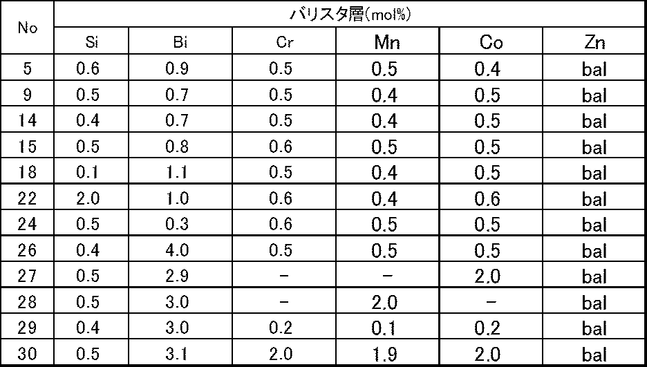


得られたサンプル1~30について、バリスタ層、拡散防止層および誘電体層についての組成を、以下の手順で分析した。
得られたバリスタ内蔵多層基板のサンプルを、外周刃切断機を用いて切断し、得られた切断片を樹脂埋めした。得られた樹脂埋めサンプルから、図1Bでしめすような構造体の断面観察像が得られる部分を狙って、クロスセクションポリッシャー(イオンポリッシャー)で断面研磨した。このようにすることで、砥粒を用いた研磨では延びてしまう電極構造を乱すことなく観察することが可能となった。
研磨面をFE-SEMで観察し、測定したい部分を狙って、FE-SEMに付属のEDX(エネルギー分散型X線分光)装置にて分析した。
分析は10μm×10μm以上の矩形面積に電子線を照射して得られたX線スペクトルを用いて解析を行った。
層中の特定の組織を分析する際は、ビーム径1μm以下で照射して得られるX線スペクトルを用いて解析を行った。含まれる結晶構造物は、X線回折法で判定した。
実施例であるサンプルNo.5、9、14、15、18、22、24および26~30について、得られたバリスタ層の組成を表2、得られた拡散防止層の組成を表3に示す。
得られた誘電体層組成は、全てのサンプルにおいて同じ値であるため、代表として、実施例であるサンプルNo.5の誘電体層の組成を分析した結果を表4に示す。
1-5.バリスタ特性の測定
バリスタ内蔵多層基板のサンプルNo.1~30に対して、アドバンテスト社製絶縁抵抗計R8340を用いて、電極間に流れる電流を、電圧を掃引しながら測定した。例としてサンプル10の測定結果を図11に示す。また、この測定結果からバリスタ特性(絶縁抵抗値、非線形定数、バリスタ電圧)を求めた。絶縁抵抗値は、電圧(V/mm)を電流値(A/cm2)で除して10を乗じた値である。非線形定数は、電流-電圧特性を両対数軸で表記した際に、電流値が1mA/cm2となる点の接線の傾きとした。接線の傾きの算出方法は、電流値が1mA/cm2となる電圧値V1(V/mm)に対して、V1+0.05V1となる範囲の測定点2点と、V1―0.05V1となる範囲の測定点2点の、合計4点に対して最小二乗法を適用し、得られた傾きを接線の傾きとした。
このようにして得られたサンプル1~30についての、絶縁抵抗率および非線形定数の値を、表5に示す。
バリスタ内蔵多層基板のサンプルNo.1~30に対して、アドバンテスト社製絶縁抵抗計R8340を用いて、電極間に流れる電流を、電圧を掃引しながら測定した。例としてサンプル10の測定結果を図11に示す。また、この測定結果からバリスタ特性(絶縁抵抗値、非線形定数、バリスタ電圧)を求めた。絶縁抵抗値は、電圧(V/mm)を電流値(A/cm2)で除して10を乗じた値である。非線形定数は、電流-電圧特性を両対数軸で表記した際に、電流値が1mA/cm2となる点の接線の傾きとした。接線の傾きの算出方法は、電流値が1mA/cm2となる電圧値V1(V/mm)に対して、V1+0.05V1となる範囲の測定点2点と、V1―0.05V1となる範囲の測定点2点の、合計4点に対して最小二乗法を適用し、得られた傾きを接線の傾きとした。
このようにして得られたサンプル1~30についての、絶縁抵抗率および非線形定数の値を、表5に示す。

比較例No.1のサンプルでは、非線形定数が7と低くなった。これは、拡散防止層が無いため、バリスタ中のBiが拡散したためであると考えられる。
比較例No.2、3および4のサンプルでは、非線形定数が低下していた。これは、拡散防止層中のSiO2量がゼロであり、焼結時に拡散防止層中にBi-Si酸化物が形成されず、バリスタ層中のBiが絶縁体層へ拡散したためであると考えられる。
比較例No.8のサンプルは、非線形定数が低下していた。これは、拡散防止層中のBi2O3量が0.01と量が少なかったため、十分なBi-Si酸化物が形成されず、またバリスタ層中のBiが絶縁体層へ拡散したためであると考えられる。
比較例No.16のサンプルは、非線形定数が19と低くなった。これは、拡散防止層中のBi2O3量が1.5であったため、Bi量が多すぎた結果、絶縁体層へ拡散したためであると考えられる。
実施例No.5~7および9~15のサンプルの結果から、拡散防止層における適切なSiO2量は、0.5~2.0、適切なBi2O3の量は0.15~1.3であると言える。
比較例No.2、3および4のサンプルでは、非線形定数が低下していた。これは、拡散防止層中のSiO2量がゼロであり、焼結時に拡散防止層中にBi-Si酸化物が形成されず、バリスタ層中のBiが絶縁体層へ拡散したためであると考えられる。
比較例No.8のサンプルは、非線形定数が低下していた。これは、拡散防止層中のBi2O3量が0.01と量が少なかったため、十分なBi-Si酸化物が形成されず、またバリスタ層中のBiが絶縁体層へ拡散したためであると考えられる。
比較例No.16のサンプルは、非線形定数が19と低くなった。これは、拡散防止層中のBi2O3量が1.5であったため、Bi量が多すぎた結果、絶縁体層へ拡散したためであると考えられる。
実施例No.5~7および9~15のサンプルの結果から、拡散防止層における適切なSiO2量は、0.5~2.0、適切なBi2O3の量は0.15~1.3であると言える。
比較例No.17のサンプルは、非線形定数が低下していた。これは、バリスタ層中のSiO2量がゼロであったため、Zn-Bi-Si-M酸化物が形成されず、バリスタ層中のBiが絶縁体層へ拡散したためであると考えられる。
比較例No.23のサンプルは、非線形定数が低下していた。これは、バリスタ層中のSiO2量が2.5であったため、Zn-Bi-Si-M酸化物が過剰に形成され、バリスタ層の緻密化が阻害されたためであると考えられる。
実施例No.10、18~22のサンプルの結果から、バリスタ層の適切なSi量は、0.1~2.0であると言える。
比較例No.23のサンプルは、非線形定数が低下していた。これは、バリスタ層中のSiO2量が2.5であったため、Zn-Bi-Si-M酸化物が過剰に形成され、バリスタ層の緻密化が阻害されたためであると考えられる。
実施例No.10、18~22のサンプルの結果から、バリスタ層の適切なSi量は、0.1~2.0であると言える。
実施例No.5、9、14、15、18、22、24、26~30のサンプルの、拡散防止層の組成分析結果を表3に示した。
拡散防止層は、Zn2SiO4を主な構成物とするZn-Si酸化物と、Bi-Si酸化物とが主な構成物であるセラミックス組成物からなり、Siが26.6~55.0mol%、Biが1.5~35.0mol%、Alが0~2.0mol%、Agが0~2.0mol%、Crが0~1.0mol%、Mnが0~1.0mol%、Coが0~1.0mol%含み、残部がZnであることを特徴とするセラミックス組成物からなることが分かった。
拡散防止層は、Zn2SiO4を主な構成物とするZn-Si酸化物と、Bi-Si酸化物とが主な構成物であるセラミックス組成物からなり、Siが26.6~55.0mol%、Biが1.5~35.0mol%、Alが0~2.0mol%、Agが0~2.0mol%、Crが0~1.0mol%、Mnが0~1.0mol%、Coが0~1.0mol%含み、残部がZnであることを特徴とするセラミックス組成物からなることが分かった。
拡散防止層の分析結果が狙い組成に対して異なっており、これはバリスタ層や絶縁層からの元素拡散のためと推測している。具体的には拡散防止層の作製工程においてAl、Ag、Cr、Mn、Coを故意に添加することがないにも関わらず、焼成後に検出されたことからAlは絶縁層から、Agは電極から、Cr、Mn、Coはバリスタ層からAg電極を介して拡散してきたと推測している。またバリスタ層中のBi量が狙い組成に対して減少していることから、バリスタ層中のBi2O3の一部は拡散防止層中に移動していると推測される。これらの要因によって拡散防止層の組成が狙い組成に対して分析結果の値がずれていると考えている。
拡散防止層のZn2SiO4を主な構成物とするZn-Si酸化物と、Bi-Si酸化物に着目した組成分析を詳細に行った結果、Zn2SiO4を主な構成物とするZn-Si酸化物はSiが30~40mol%、Biが0~2.0mol%、Alが0~1.0mol%、Agが0~1.0mol%、Crが0~0.4mol%、Mnが0~0.4mol%、Coが0~0.4mol%含み、残部がZnであることを特徴とし、Bi-Si化合物はSiが30.0~70.0mol%、Biが5.0~30.0mol%、Alが0~8.0mol%、Agが0~15.0mol%、Crが0~0.6mol%、Mnが0~0.6mol%、Coが0~0.6mol%含むことを特徴とするセラミックス組成物であることが分かった。
拡散防止層中のBi-Si化合物にAgやAlを多く含んでいることから焼成時の拡散現象は拡散防止層中のBi-Si化合物を介して起こっていると推測され、このような元素拡散が各層の密着を良好にしていると推測している。
バリスタ層は主相がZnOであり、そのZnO粒子の粒界または粒界三重点にZn-Bi-Si-M酸化物(MはCo、Mn、Crのいずれか一つ以上)またはZn-Si-M酸化物(MはCo、Mn、Crのいずれか一つ以上)もしくは両方の酸化物が存在しており、金属元素換算でSiが0.1~2.0mol%、Biが0.3~4.0mol%、Crが2.0mol%以下、Mnが2.0mol%以下、Coが2.0mol%以下、残部がZnであることを特徴とするセラミックスであることが分かった。
実施例No.5のサンプルのように、拡散防止層の設置とバリスタ層へのSi添加を併せた時にバリスタ層中にZn-Bi-Si-M酸化物(MはCo、Mn、Crのいずれか一つ以上)とZn-Si-M酸化物(MはCo、Mn、Crのいずれか一つ以上)が形成されていた。バリスタ層中のZn-Bi-Si-M酸化物またはZn-Si-M酸化物に着目して分析した結果、Zn-Bi-Si-M酸化物は金属元素換算でSiが0.5~4.0mol%、Biが50.0~70.0mol%、Crが0.1~8.0mol%、Mnが0.2~3.0mol%、Coが0.2~3.0mol%、残部がZnであることを特徴とし、Zn-Si-M酸化物はSiが28.0~40.0mol%、Biが1.0mol%以下、Crが0~1.0mol%、Mnが0.1~1.5mol%、Coが0~2.4mol%以下、残部がZnであることを特徴とするセラミックスであることが分かった。
拡散防止層の設置とバリスタ層へのSi添加を併せた時にバリスタ層中にZn-Bi-Si-M酸化物が形成されていた。これはBiとSiが焼成時に反応することでBiがバリスタ層外に拡散することを防いだ結果、形成されたと考えている。拡散防止層が必須である要因としてBiとSiが反応する温度とBiの供給源であるBi2O3の融点が近いことが挙げられる。拡散防止層が無い場合、BiがSiと反応する前にBi2O3が液化してバリスタ層外の絶縁層へ拡散してしまったと推測している。そこでBiを多く含む拡散防止層を設けることで拡散速度を遅くし、バリスタ層の外へ拡散する前にSiと反応させることが可能となり、実施例のような特性が得られるバリスタ組織になったと推測している。またZn-Si-M酸化物はBiと反応しなかったSiがZnと反応して形成していると考えている。
・実施例2
2-1.バリスタ層粉シート作製
表6に示す組成となるように、ZnO、Bi2O3、Co3O4、Mn3O4、Cr2O3、Bi4Si3O12を秤量し、ボールミル容器中にエタノール、ジルコニアボールとともに投入して、100rpmで20時間ボールミル混合した。Bi4Si3O12は、Bi2O3およびSiO2を、BiとSiがBi4Si3O12組成の割合となるように秤量混合し、ボールミル容器中にエタノール、ジルコニアボールとともに投入して、100rpmで20時間ボールミル混合し、乾燥して得られた混合粉を大気中700℃で熱処理することによって作製した。Bi4Si3O12の添加によって足りない量のBiは、Bi2O3を添加することで調整した。なお、本実施例における組成は、金属元素換算のmol%で示している。すなわち、それぞれの酸化物が含有する酸素原子を考慮せず、酸素と結びついている金属原子のみを考慮して、モル比率を算出し求めたものであり、表6では、Zn、Bi、Si、Co、Mn、Crのそれぞれの金属元素のmol%を示している。
2-1.バリスタ層粉シート作製
表6に示す組成となるように、ZnO、Bi2O3、Co3O4、Mn3O4、Cr2O3、Bi4Si3O12を秤量し、ボールミル容器中にエタノール、ジルコニアボールとともに投入して、100rpmで20時間ボールミル混合した。Bi4Si3O12は、Bi2O3およびSiO2を、BiとSiがBi4Si3O12組成の割合となるように秤量混合し、ボールミル容器中にエタノール、ジルコニアボールとともに投入して、100rpmで20時間ボールミル混合し、乾燥して得られた混合粉を大気中700℃で熱処理することによって作製した。Bi4Si3O12の添加によって足りない量のBiは、Bi2O3を添加することで調整した。なお、本実施例における組成は、金属元素換算のmol%で示している。すなわち、それぞれの酸化物が含有する酸素原子を考慮せず、酸素と結びついている金属原子のみを考慮して、モル比率を算出し求めたものであり、表6では、Zn、Bi、Si、Co、Mn、Crのそれぞれの金属元素のmol%を示している。
得られた混合原料を取り出して乾燥後、エタノール、PVBおよび可塑剤と混合してスラリー状の混合原料を作製した。このとき、スラリーに占めるPVBの含有率は10重量%とした。
このスラリー状の混合原料を用い、ドクターブレード法により成型し、バリスタ層粉シートを作製した。
このスラリー状の混合原料を用い、ドクターブレード法により成型し、バリスタ層粉シートを作製した。
2-2.拡散防止層粉シートの作製
拡散防止層の組成を表6に示す組成とした他は実施例1と同様にして、拡散防止層粉シートを作製した。
拡散防止層の組成を表6に示す組成とした他は実施例1と同様にして、拡散防止層粉シートを作製した。
2-3.誘電体層粉シートの作製
実施例1と同様にして、誘電体層粉シートを作製した。
実施例1と同様にして、誘電体層粉シートを作製した。
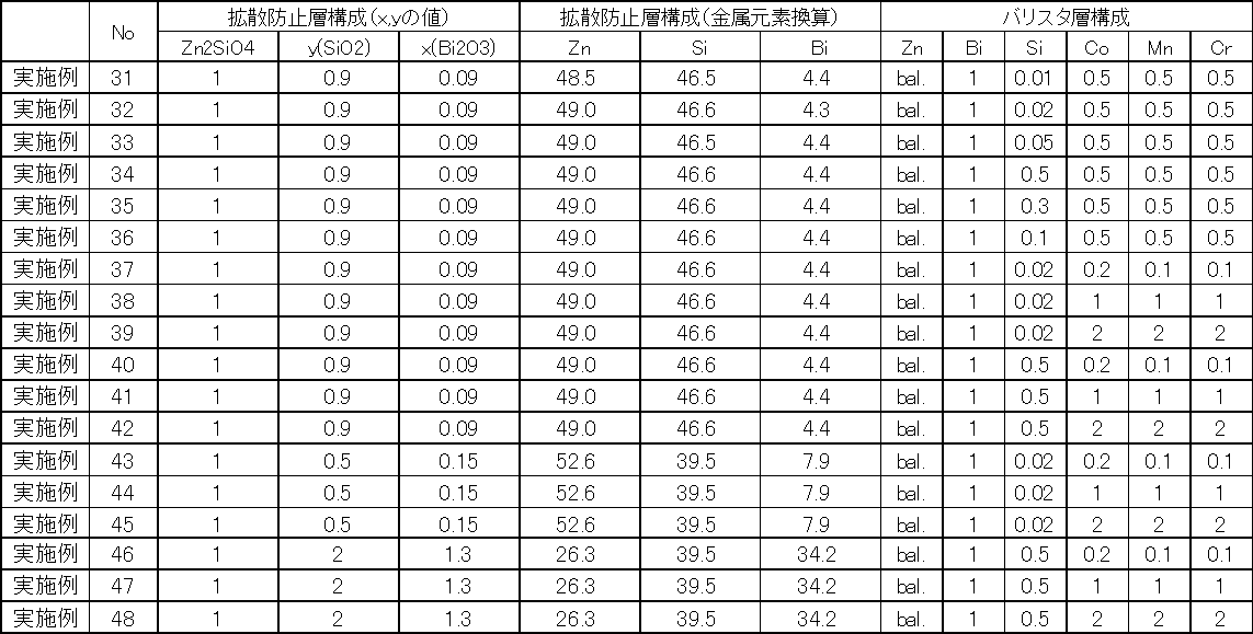
得られたバリスタ層粉シート、拡散防止層粉シートおよび誘電体層粉シートを用いて、図7A~図7Dおよび上述した段落0097~0101に示す手順により積層し、85℃で20MPaで10分間荷重を加えた。このようにして得られた混合原料シート積層体を、昇温速度200℃/hで昇温し、900℃で2時間焼成して、バリスタ内蔵多層基板を得た。
2-4.バリスタ特性および空孔率の測定
得られたバリスタ内蔵多層基板のサンプルNo.31~48に対して、アドバンテスト社製絶縁抵抗計R8340を用いて、電極間に流れる電流を、電圧を掃引しながら測定した。また、この測定結果からバリスタ特性(絶縁抵抗値、非線形定数、バリスタ電圧)を求めた。絶縁抵抗値は、電圧(V/mm)を電流値(A/cm2)で除して10を乗じた値である。非線形定数は、電流-電圧特性を両対数軸で表記した際に、電流値が1mA/cm2となる点の接線の傾きとした。接線の傾きの算出方法は、電流値が1mA/cm2となる電圧値V1(V/mm)に対して、V1+0.05V1となる範囲の測定点2点と、V1―0.05V1となる範囲の測定点2点の、合計4点に対して最小二乗法を適用し、得られた傾きを接線の傾きとした。
このようにして得られたサンプルNo.31~48についての、絶縁抵抗率および非線形係数の値を、表7に示す。また、サンプルNo.31~48の空孔率を求めた。空孔率は、バリスタ層を機械加工により切断し、断面を研磨した後、研磨面から測定する視野をランダムに5つ選択し、各視野を走査型電子顕微鏡によって観察し、それぞれの視野に対して、視野内における空孔部分の面積割合を算出した。具体的には、算出方法は、観察像を紙面に印刷し空孔部のみを黒く塗りつぶした後スキャナで読込み、Scandium(OLYMPUS社製)を用いた画像処理によって、観察像中の空孔とそれ以外の部分を二値化することにより、視野内の空孔部分の面積割合を求めた。5つの視野における空孔部分の面積割合の平均値を求めて、バリスタ層の空孔率(%)とした。図12にサンプル32の断面写真を示す。
得られたバリスタ内蔵多層基板のサンプルNo.31~48に対して、アドバンテスト社製絶縁抵抗計R8340を用いて、電極間に流れる電流を、電圧を掃引しながら測定した。また、この測定結果からバリスタ特性(絶縁抵抗値、非線形定数、バリスタ電圧)を求めた。絶縁抵抗値は、電圧(V/mm)を電流値(A/cm2)で除して10を乗じた値である。非線形定数は、電流-電圧特性を両対数軸で表記した際に、電流値が1mA/cm2となる点の接線の傾きとした。接線の傾きの算出方法は、電流値が1mA/cm2となる電圧値V1(V/mm)に対して、V1+0.05V1となる範囲の測定点2点と、V1―0.05V1となる範囲の測定点2点の、合計4点に対して最小二乗法を適用し、得られた傾きを接線の傾きとした。
このようにして得られたサンプルNo.31~48についての、絶縁抵抗率および非線形係数の値を、表7に示す。また、サンプルNo.31~48の空孔率を求めた。空孔率は、バリスタ層を機械加工により切断し、断面を研磨した後、研磨面から測定する視野をランダムに5つ選択し、各視野を走査型電子顕微鏡によって観察し、それぞれの視野に対して、視野内における空孔部分の面積割合を算出した。具体的には、算出方法は、観察像を紙面に印刷し空孔部のみを黒く塗りつぶした後スキャナで読込み、Scandium(OLYMPUS社製)を用いた画像処理によって、観察像中の空孔とそれ以外の部分を二値化することにより、視野内の空孔部分の面積割合を求めた。5つの視野における空孔部分の面積割合の平均値を求めて、バリスタ層の空孔率(%)とした。図12にサンプル32の断面写真を示す。
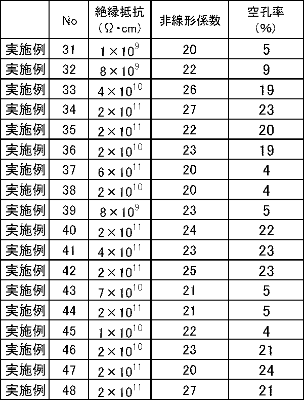
表7の結果から、SiをBi4Si3O12の形で添加し、Siの組成範囲を0.01~0.3mol%とすることにより、非線形定数20以上、空孔率20%以下の、緻密なバリスタ特性に優れたバリスタ層を有するバリスタ内蔵多層基板が得られたことがわかる。
本出願は、出願日が2015年3月31日である日本国特許出願、特願第2015-073187号および出願日が2015年12月10日である日本国特許出願、特願第2015-241198号を基礎出願とする優先権主張を伴い、特願第2015-073187号および特願第2015-241198号は参照することにより本明細書に取り込まれる。
10:第1誘電体層(焼成前は混合原料シート)
12:第1拡散防止層(焼成前は混合原料シートまたはペースト)
14:バリスタ層含有絶縁体層(焼成前は混合原料シート)
15:バリスタ層(焼成前は混合原料シートまたはペースト)
16:第2拡散防止層(焼成前は混合原料シートまたはペースト)
18:第2誘電体層(焼成前は混合原料シート)
20:第1内部電極(焼成前は電極層ペースト)
22:第2内部電極(焼成前は電極層ペースト)
24:第1貫通電極(焼成前は電極層ペースト)
26:第2貫通電極(焼成前は電極層ペースト)
30、38:誘電体層粉シート
32、36:拡散防止層粉シートまたはペースト
34:誘電体層粉シート
35:バリスタ層粉シートまたはペースト
40:第1貫通孔
41:第2貫通孔
42:バリスタ用貫通孔
150、160、170、180、190:積層体
100、200、300、400:多層基板
D1、D2:電極間距離
S1、S2:電流断面積
12:第1拡散防止層(焼成前は混合原料シートまたはペースト)
14:バリスタ層含有絶縁体層(焼成前は混合原料シート)
15:バリスタ層(焼成前は混合原料シートまたはペースト)
16:第2拡散防止層(焼成前は混合原料シートまたはペースト)
18:第2誘電体層(焼成前は混合原料シート)
20:第1内部電極(焼成前は電極層ペースト)
22:第2内部電極(焼成前は電極層ペースト)
24:第1貫通電極(焼成前は電極層ペースト)
26:第2貫通電極(焼成前は電極層ペースト)
30、38:誘電体層粉シート
32、36:拡散防止層粉シートまたはペースト
34:誘電体層粉シート
35:バリスタ層粉シートまたはペースト
40:第1貫通孔
41:第2貫通孔
42:バリスタ用貫通孔
150、160、170、180、190:積層体
100、200、300、400:多層基板
D1、D2:電極間距離
S1、S2:電流断面積
Claims (18)
- 順に積層されている、第1誘電体層、第1拡散防止層、バリスタ層、第2拡散防止層および第2誘電体層と、前記バリスタ層のいずれかの主面にそれぞれ配置された第1内部電極および第2内部電極とを有し、
前記第1誘電体層および前記第2誘電体層は、ボイドが面積比率で5%未満であり、電気抵抗率が1010Ω・cm以上であり、比誘電率が6~9であり、
前記第1拡散防止層および前記第2拡散防止層は、Zn2SiO4を主成分とするZn-Si酸化物と、Bi-Si酸化物とを含み、
前記バリスタ層は、主相がZnOであり、前記ZnOの粒界または粒界三重点にZn-Bi-Si-M酸化物(MはCo、Mn、Crのいずれか一つ以上)および/またはZn-Si-M酸化物(MはCo、Mn、Crのいずれか一つ以上)が存在していることを特徴とする、バリスタ内蔵多層基板。 - 前記バリスタ層は、Siを含む金属元素全体を100mol%としたとき、
Znを90.0mol%以上、Siを0.01~2.0mol%およびBiを0.3~4.0mol%含み、0.1~2.0mol%のCr、0.1~4.0mol%のMnおよび0.1~2.0mol%のCoから選択されるいずれか1種以上を含むことを特徴とする、請求項1に記載のバリスタ内蔵多層基板。 - 前記バリスタ層は、Siの組成が0.1~2.0mol%であることを特徴とする、請求項2に記載のバリスタ内蔵多層基板。
- 前記バリスタ層は、Siの組成が0.01~0.3mol%であることを特徴とする、請求項2に記載のバリスタ内蔵多層基板。
- 前記バリスタ層は、残部が不可避的不純物であることを特徴とする、請求項2~4のいずれか1項に記載のバリスタ内蔵多層基板。
- 前記バリスタ層は、0.1~2.0mol%のScおよび0.1~4.0mol%のBから成る群から選択される少なくとも1つをさらに含むことを特徴とする請求項2~5のいずれか1項に記載のバリスタ内蔵多層基板。
- 前記バリスタ層は、アンチモン(Sb)、希土類元素および錫(Sn)のそれぞれの含有量が不純物レベル以下であることを特徴とする、請求項2~6のいずれか1項に記載のバリスタ内蔵多層基板。
- 前記第1拡散防止層および前記第2拡散防止層は、Siを含む金属元素全体を100mol%としたとき、
Znを30mol%以上、Siを26.6~55.0mol%、Biを1.5~35.0mol%含むことを特徴とする、請求項1~7のいずれか1項に記載のバリスタ内蔵多層基板。 - 前記第1誘電体層および前記第2誘電体層は、Al-Si-Sr酸化物を主成分とし、SrAl2Si2O8、Al2O3およびTiO2を含むセラミックス組成物であることを特徴とする、請求項1~8のいずれか1項に記載のバリスタ内蔵多層基板。
- 前記第1誘電体層および前記第2誘電体層は、Siを含む金属元素全体を100mol%としたとき、
Alを23.6~63.5mol%、Siを24.2~60.0mol%、Srを5.1~26.8mol%、Tiを0.1~2.8mol%、Biを0.1~0.7mol%、Naを0.1~3.4mol%、Kを0~1.2mol%、Coを0~0.5mol%、Cuを0.1~0.7mol%、Mnを0.1~0.6mol%、Agを0.1~2.0mol%およびZrを0.4~1.7mol%含むセラミックス組成物であることを特徴とする、請求項1~9のいずれか1項に記載のバリスタ内蔵多層基板。 - 前記第1内部電極は、前記バリスタ層の一方の主面に配置され、前記第1誘電体層を貫通する第1貫通電極と電気的に接続されており、
前記第2内部電極は、前記バリスタ層の他方の主面に配置され、前記第2誘電体層を貫通する第2貫通電極と電気的に接続されている、請求項1~10のいずれか1項に記載のバリスタ内蔵多層基板。 - 前記第1貫通電極は、前記第1誘電体層と前記第1拡散防止層とを貫通しており、前記第2貫通電極は、前記第2誘電体層と前記第2拡散防止層とを貫通している、請求項11に記載のバリスタ内蔵多層基板。
- 前記第1内部電極および前記第2内部電極は、前記バリスタ層の1つの主面に離間して配置され、前記第1内部電極は、前記第1誘電体層を貫通する第1貫通電極と電気的に接続され、前記第2内部電極は、前記第1誘電体層を貫通する第2貫通電極と電気的に接続されている、請求項1~10のいずれか1項に記載のバリスタ内蔵多層基板。
- 前記第1貫通電極および前記第2貫通電極は、前記第1誘電体層と前記第1拡散防止層とを貫通している、請求項13に記載のバリスタ内蔵多層基板。
- 1)酸化亜鉛と、酸化ビスマスと、酸化ケイ素と、酸化コバルト、酸化クロムおよび酸化マンガンから選択される1種以上とを混合して、酸化亜鉛を主成分とし、酸化ビスマスをビスマス換算で0.3~4.0mol%、および酸化ケイ素をシリコン換算で0.01~2.0mol%含み、コバルト換算で0.1~2.5mol%の酸化コバルト、クロム換算で0.1~2.5mol%の酸化クロムおよびマンガン換算で0.1~5.0mol%酸化マンガンから選ばれる1種以上を含む第1混合原料を得て、前記第1混合原料を含むバリスタ層粉シートを形成する工程と、
2)Zn2SiO4とBi2O3とSiO2とを、モル比率で以下の組成式(1)を満たすように混合して、第2混合原料を得て、前記第2混合原料を含む拡散防止層粉シートを形成する工程と、
Zn2SiO4+xBi2O3+ySiO2(0.06≦x≦1.30、0.50≦y≦2.00) (1)
3)少なくとも、酸化アルミニウムと、酸化ケイ素と、炭酸ストロンチウムと、酸化チタンと、酸化ビスマスと、酸化ナトリウムと、炭酸カリウムと、酸化銅と、酸化マンガンと、酸化銀と、酸化ジルコニウムとを混合して、Alを23.6~63.5mol%、Siを24.2~60.0mol%、Srを5.1~26.8mol%、Tiを0.1~2.8mol%、Biを0.1~0.7mol%、Naを0.1~3.4mol%、Kを0~1.2mol%、Cuを0.1~0.7mol%、Mnを0.1~0.6mol%、Agを0.1~2.0mol%およびZrを0.4~1.7mol%含む第3混合原料を得て、前記第3混合原料を含む誘電体層粉シートを形成する工程と、
4)順に、前記誘電体層粉シート、前記拡散防止層粉シート、前記バリスタ層粉シート、前記拡散防止層粉シートおよび前記誘電体層粉シートを配置して、積層体を得る工程と、
5)前記積層体を850℃~900℃で焼成する工程と、
を含むことを特徴とするバリスタ内蔵多層基板の製造方法。 - 1)酸化亜鉛と、酸化ビスマスと、酸化ケイ素と、酸化コバルト、酸化クロムおよび酸化マンガンから選択される1種以上とを混合して、酸化亜鉛を主成分とし、酸化ビスマスをビスマス換算で0.3~4.0mol%、および酸化ケイ素をシリコン換算で0.01~2.0mol%含み、コバルト換算で0.1~2.5mol%の酸化コバルト、クロム換算で0.1~2.5mol%の酸化クロムおよびマンガン換算で0.1~5.0mol%酸化マンガンから選ばれる1種以上を含む第1混合原料を得て、前記第1混合原料を含むバリスタ層粉ペーストを形成する工程と、
2)Zn2SiO4とBi2O3とSiO2とを、モル比率で以下の組成式(2)を満たすように混合して、第2混合原料を得て、前記第2混合原料を含む拡散防止層粉ペーストを形成する工程と、
Zn2SiO4+xBi2O3+ySiO2(0.06≦x≦1.30、0.50≦y≦2.00) (2)
3)少なくとも、酸化アルミニウムと、酸化ケイ素と、炭酸ストロンチウムと、酸化チタンと、酸化ビスマスと、酸化ナトリウムと、炭酸カリウムと、酸化銅と、酸化マンガンと、酸化銀と、酸化ジルコニウムとを混合して、Alを23.6~63.5mol%、Siを24.2~60.0mol%、Srを5.1~26.8mol%、Tiを0.1~2.8mol%、Biを0.1~0.7mol%、Naを0.1~3.4mol%、Kを0~1.2mol%、Cuを0.1~0.7mol%、Mnを0.1~0.6mol%、Agを0.1~2.0mol%およびZrを0.4~1.7mol%含む第3混合原料を得て、前記第3混合原料を含む誘電体層粉シートを形成する工程と、
4)順に、前記誘電体層粉シート、前記拡散防止層粉ペースト、前記バリスタ層粉ペースト、前記拡散防止層粉ペーストおよび前記誘電体層粉シートを配置して、積層体を得る工程と、
5)前記積層体を850℃~900℃で焼成する工程と、
を含むことを特徴とするバリスタ内蔵多層基板の製造方法。 - 1)酸化亜鉛と、ビスマス・シリコン酸化化合物と、酸化ビスマスと、酸化コバルト、酸化クロムおよび酸化マンガンから選択される1種以上とを混合して、酸化亜鉛を主成分とし、酸化ビスマスをビスマス換算で0.3~4.0mol%、および酸化ケイ素をシリコン換算で0.01~2.0mol%含み、コバルト換算で0.1~2.5mol%の酸化コバルト、クロム換算で0.1~2.5mol%の酸化クロムおよびマンガン換算で0.1~5.0mol%酸化マンガンから選ばれる1種以上を含む第1混合原料を得て、前記第1混合原料を含むバリスタ層粉シートを形成する工程と、
2)Zn2SiO4とBi2O3とSiO2とを、モル比率で以下の組成式(3)を満たすように混合して、第2混合原料を得て、前記第2混合原料を含む拡散防止層粉シートを形成する工程と、
Zn2SiO4+xBi2O3+ySiO2(0.06≦x≦1.30、0.50≦y≦2.00) (3)
3)少なくとも、酸化アルミニウムと、酸化ケイ素と、炭酸ストロンチウムと、酸化チタンと、酸化ビスマスと、酸化ナトリウムと、炭酸カリウムと、酸化銅と、酸化マンガンと、酸化銀と、酸化ジルコニウムとを混合して、Alを23.6~63.5mol%、Siを24.2~60.0mol%、Srを5.1~26.8mol%、Tiを0.1~2.8mol%、Biを0.1~0.7mol%、Naを0.1~3.4mol%、Kを0~1.2mol%、Cuを0.1~0.7mol%、Mnを0.1~0.6mol%、Agを0.1~2.0mol%およびZrを0.4~1.7mol%含む第3混合原料を得て、前記第3混合原料を含む誘電体層粉シートを形成する工程と、
4)順に、前記誘電体層粉シート、前記拡散防止層粉シート、前記バリスタ層粉シート、前記拡散防止層粉シートおよび前記誘電体層粉シートを配置して、積層体を得る工程と、
5)前記積層体を850℃~900℃で焼成する工程と、
を含むことを特徴とするバリスタ内蔵多層基板の製造方法。 - 1)酸化亜鉛と、ビスマス・シリコン酸化化合物と、酸化ビスマスと、酸化コバルト、酸化クロムおよび酸化マンガンから選択される1種以上とを混合して、酸化亜鉛を主成分とし、酸化ビスマスをビスマス換算で0.3~4.0mol%、および酸化ケイ素をシリコン換算で0.01~2.0mol%含み、コバルト換算で0.1~2.5mol%の酸化コバルト、クロム換算で0.1~2.5mol%の酸化クロムおよびマンガン換算で0.1~5.0mol%酸化マンガンから選ばれる1種以上を含む第1混合原料を得て、前記第1混合原料を含むバリスタ層粉ペーストを形成する工程と、
2)Zn2SiO4とBi2O3とSiO2とを、モル比率で以下の組成式(4)を満たすように混合して、第2混合原料を得て、前記第2混合原料を含む拡散防止層粉ペーストを形成する工程と、
Zn2SiO4+xBi2O3+ySiO2(0.06≦x≦1.30、0.50≦y≦2.00) (4)
3)少なくとも、酸化アルミニウムと、酸化ケイ素と、炭酸ストロンチウムと、酸化チタンと、酸化ビスマスと、酸化ナトリウムと、炭酸カリウムと、酸化銅と、酸化マンガンと、酸化銀と、酸化ジルコニウムとを混合して、Alを23.6~63.5mol%、Siを24.2~60.0mol%、Srを5.1~26.8mol%、Tiを0.1~2.8mol%、Biを0.1~0.7mol%、Naを0.1~3.4mol%、Kを0~1.2mol%、Cuを0.1~0.7mol%、Mnを0.1~0.6mol%、Agを0.1~2.0mol%およびZrを0.4~1.7mol%含む第3混合原料を得て、前記第3混合原料を含む誘電体層粉シートを形成する工程と、
4)順に、前記誘電体層粉シート、前記拡散防止層粉ペースト、前記バリスタ層粉ペースト、前記拡散防止層粉ペーストおよび前記誘電体層粉シートを配置して、積層体を得る工程と、
5)前記積層体を850℃~900℃で焼成する工程と、
を含むことを特徴とするバリスタ内蔵多層基板の製造方法。
Priority Applications (1)
| Application Number | Priority Date | Filing Date | Title |
|---|---|---|---|
| JP2017509556A JP6777070B2 (ja) | 2015-03-31 | 2016-03-17 | バリスタ内蔵多層基板およびその製造方法 |
Applications Claiming Priority (4)
| Application Number | Priority Date | Filing Date | Title |
|---|---|---|---|
| JP2015-073187 | 2015-03-31 | ||
| JP2015073187 | 2015-03-31 | ||
| JP2015-241198 | 2015-12-10 | ||
| JP2015241198 | 2015-12-10 |
Publications (1)
| Publication Number | Publication Date |
|---|---|
| WO2016158464A1 true WO2016158464A1 (ja) | 2016-10-06 |
Family
ID=57004298
Family Applications (1)
| Application Number | Title | Priority Date | Filing Date |
|---|---|---|---|
| PCT/JP2016/058555 Ceased WO2016158464A1 (ja) | 2015-03-31 | 2016-03-17 | バリスタ内蔵多層基板およびその製造方法 |
Country Status (2)
| Country | Link |
|---|---|
| JP (1) | JP6777070B2 (ja) |
| WO (1) | WO2016158464A1 (ja) |
Cited By (1)
| Publication number | Priority date | Publication date | Assignee | Title |
|---|---|---|---|---|
| CN110467818A (zh) * | 2019-08-23 | 2019-11-19 | 国网天津市电力公司 | 一种微-纳米混合ZnO非线性硅橡胶复合绝缘子及制备工艺 |
Citations (5)
| Publication number | Priority date | Publication date | Assignee | Title |
|---|---|---|---|---|
| JPS5454296A (en) * | 1977-10-06 | 1979-04-28 | Marukon Denshi Kk | Method of producing voltage nonnlinear resistor |
| JP2004196652A (ja) * | 2002-12-06 | 2004-07-15 | Hitachi Metals Ltd | 高強度低温焼成セラミック組成物及びその製造方法、並びにこれを用いた積層電子部品 |
| WO2004089049A1 (ja) * | 2003-03-28 | 2004-10-14 | Tdk Corporation | 多層基板およびその製造方法 |
| JP2006253459A (ja) * | 2005-03-11 | 2006-09-21 | Matsushita Electric Ind Co Ltd | 積層セラミック電子部品 |
| JP2013115107A (ja) * | 2011-11-25 | 2013-06-10 | Panasonic Corp | バリスタ内蔵セラミック基板 |
-
2016
- 2016-03-17 JP JP2017509556A patent/JP6777070B2/ja not_active Expired - Fee Related
- 2016-03-17 WO PCT/JP2016/058555 patent/WO2016158464A1/ja not_active Ceased
Patent Citations (5)
| Publication number | Priority date | Publication date | Assignee | Title |
|---|---|---|---|---|
| JPS5454296A (en) * | 1977-10-06 | 1979-04-28 | Marukon Denshi Kk | Method of producing voltage nonnlinear resistor |
| JP2004196652A (ja) * | 2002-12-06 | 2004-07-15 | Hitachi Metals Ltd | 高強度低温焼成セラミック組成物及びその製造方法、並びにこれを用いた積層電子部品 |
| WO2004089049A1 (ja) * | 2003-03-28 | 2004-10-14 | Tdk Corporation | 多層基板およびその製造方法 |
| JP2006253459A (ja) * | 2005-03-11 | 2006-09-21 | Matsushita Electric Ind Co Ltd | 積層セラミック電子部品 |
| JP2013115107A (ja) * | 2011-11-25 | 2013-06-10 | Panasonic Corp | バリスタ内蔵セラミック基板 |
Cited By (1)
| Publication number | Priority date | Publication date | Assignee | Title |
|---|---|---|---|---|
| CN110467818A (zh) * | 2019-08-23 | 2019-11-19 | 国网天津市电力公司 | 一种微-纳米混合ZnO非线性硅橡胶复合绝缘子及制备工艺 |
Also Published As
| Publication number | Publication date |
|---|---|
| JP6777070B2 (ja) | 2020-10-28 |
| JPWO2016158464A1 (ja) | 2018-01-25 |
Similar Documents
| Publication | Publication Date | Title |
|---|---|---|
| CN111724992B (zh) | 层叠陶瓷电容器 | |
| KR101687575B1 (ko) | 적층 세라믹 콘덴서 | |
| CN108467266B (zh) | 电介质组合物、电介质元件、电子部件和层叠电子部件 | |
| CN103140904B (zh) | 积层陶瓷电容器 | |
| CN103370754B (zh) | 带变阻器功能的层叠型半导体陶瓷电容器及其制造方法 | |
| CN101350241B (zh) | 可变电阻 | |
| US10262796B2 (en) | Dielectric composition and electronic component | |
| US20150279565A1 (en) | Multi-layer ceramic capacitor | |
| JP2018137298A (ja) | 積層セラミックコンデンサ | |
| JP5163097B2 (ja) | バリスタ | |
| JP2017028254A (ja) | 積層セラミックコンデンサ | |
| KR20230000965A (ko) | 유전체, 적층 세라믹 콘덴서, 유전체의 제조 방법, 및 적층 세라믹 콘덴서의 제조 방법 | |
| KR20220102568A (ko) | 유전체, 세라믹 전자 부품, 유전체의 제조 방법, 및 세라믹 전자 부품의 제조 방법 | |
| JP4461679B2 (ja) | 誘電体磁器組成物および電子部品 | |
| JP2014067775A (ja) | 積層セラミックコンデンサ | |
| WO2021131819A1 (ja) | コンデンサ | |
| KR100673916B1 (ko) | 유전체 자기 조성물 및 전자 부품 | |
| CN112687467B (zh) | 陶瓷电子器件及其制造方法 | |
| JP6387969B2 (ja) | バリスタ用焼結体およびこれを用いた多層基板、ならびにそれらの製造方法 | |
| JP5195857B2 (ja) | 積層型電子部品 | |
| JP7842278B2 (ja) | 積層セラミック電子部品および誘電体磁器組成物 | |
| JP6777070B2 (ja) | バリスタ内蔵多層基板およびその製造方法 | |
| JP6766510B2 (ja) | 誘電体組成物及び電子部品 | |
| JP2016225404A (ja) | 酸化亜鉛系バリスタ用焼結体およびこれを用いた多層基板、ならびにそれらの製造方法 | |
| JP2018139261A (ja) | コンデンサ |
Legal Events
| Date | Code | Title | Description |
|---|---|---|---|
| 121 | Ep: the epo has been informed by wipo that ep was designated in this application |
Ref document number: 16772347 Country of ref document: EP Kind code of ref document: A1 |
|
| ENP | Entry into the national phase |
Ref document number: 2017509556 Country of ref document: JP Kind code of ref document: A |
|
| NENP | Non-entry into the national phase |
Ref country code: DE |
|
| 122 | Ep: pct application non-entry in european phase |
Ref document number: 16772347 Country of ref document: EP Kind code of ref document: A1 |