WO2016152720A1 - ホログラムシート、応力発光シートおよび偽造防止用紙 - Google Patents
ホログラムシート、応力発光シートおよび偽造防止用紙 Download PDFInfo
- Publication number
- WO2016152720A1 WO2016152720A1 PCT/JP2016/058500 JP2016058500W WO2016152720A1 WO 2016152720 A1 WO2016152720 A1 WO 2016152720A1 JP 2016058500 W JP2016058500 W JP 2016058500W WO 2016152720 A1 WO2016152720 A1 WO 2016152720A1
- Authority
- WO
- WIPO (PCT)
- Prior art keywords
- stress
- layer
- hologram
- light emitting
- stimulated luminescent
- Prior art date
- Legal status (The legal status is an assumption and is not a legal conclusion. Google has not performed a legal analysis and makes no representation as to the accuracy of the status listed.)
- Ceased
Links
Images
















Classifications
-
- G—PHYSICS
- G03—PHOTOGRAPHY; CINEMATOGRAPHY; ANALOGOUS TECHNIQUES USING WAVES OTHER THAN OPTICAL WAVES; ELECTROGRAPHY; HOLOGRAPHY
- G03H—HOLOGRAPHIC PROCESSES OR APPARATUS
- G03H1/00—Holographic processes or apparatus using light, infrared or ultraviolet waves for obtaining holograms or for obtaining an image from them; Details peculiar thereto
- G03H1/02—Details of features involved during the holographic process; Replication of holograms without interference recording
- G03H1/0252—Laminate comprising a hologram layer
- G03H1/0256—Laminate comprising a hologram layer having specific functional layer
-
- B—PERFORMING OPERATIONS; TRANSPORTING
- B32—LAYERED PRODUCTS
- B32B—LAYERED PRODUCTS, i.e. PRODUCTS BUILT-UP OF STRATA OF FLAT OR NON-FLAT, e.g. CELLULAR OR HONEYCOMB, FORM
- B32B27/00—Layered products comprising a layer of synthetic resin
- B32B27/18—Layered products comprising a layer of synthetic resin characterised by the use of special additives
-
- B—PERFORMING OPERATIONS; TRANSPORTING
- B42—BOOKBINDING; ALBUMS; FILES; SPECIAL PRINTED MATTER
- B42D—BOOKS; BOOK COVERS; LOOSE LEAVES; PRINTED MATTER CHARACTERISED BY IDENTIFICATION OR SECURITY FEATURES; PRINTED MATTER OF SPECIAL FORMAT OR STYLE NOT OTHERWISE PROVIDED FOR; DEVICES FOR USE THEREWITH AND NOT OTHERWISE PROVIDED FOR; MOVABLE-STRIP WRITING OR READING APPARATUS
- B42D25/00—Information-bearing cards or sheet-like structures characterised by identification or security features; Manufacture thereof
- B42D25/30—Identification or security features, e.g. for preventing forgery
- B42D25/328—Diffraction gratings; Holograms
-
- B—PERFORMING OPERATIONS; TRANSPORTING
- B42—BOOKBINDING; ALBUMS; FILES; SPECIAL PRINTED MATTER
- B42D—BOOKS; BOOK COVERS; LOOSE LEAVES; PRINTED MATTER CHARACTERISED BY IDENTIFICATION OR SECURITY FEATURES; PRINTED MATTER OF SPECIAL FORMAT OR STYLE NOT OTHERWISE PROVIDED FOR; DEVICES FOR USE THEREWITH AND NOT OTHERWISE PROVIDED FOR; MOVABLE-STRIP WRITING OR READING APPARATUS
- B42D25/00—Information-bearing cards or sheet-like structures characterised by identification or security features; Manufacture thereof
- B42D25/30—Identification or security features, e.g. for preventing forgery
- B42D25/351—Translucent or partly translucent parts, e.g. windows
-
- B—PERFORMING OPERATIONS; TRANSPORTING
- B42—BOOKBINDING; ALBUMS; FILES; SPECIAL PRINTED MATTER
- B42D—BOOKS; BOOK COVERS; LOOSE LEAVES; PRINTED MATTER CHARACTERISED BY IDENTIFICATION OR SECURITY FEATURES; PRINTED MATTER OF SPECIAL FORMAT OR STYLE NOT OTHERWISE PROVIDED FOR; DEVICES FOR USE THEREWITH AND NOT OTHERWISE PROVIDED FOR; MOVABLE-STRIP WRITING OR READING APPARATUS
- B42D25/00—Information-bearing cards or sheet-like structures characterised by identification or security features; Manufacture thereof
- B42D25/30—Identification or security features, e.g. for preventing forgery
- B42D25/355—Security threads
-
- B—PERFORMING OPERATIONS; TRANSPORTING
- B42—BOOKBINDING; ALBUMS; FILES; SPECIAL PRINTED MATTER
- B42D—BOOKS; BOOK COVERS; LOOSE LEAVES; PRINTED MATTER CHARACTERISED BY IDENTIFICATION OR SECURITY FEATURES; PRINTED MATTER OF SPECIAL FORMAT OR STYLE NOT OTHERWISE PROVIDED FOR; DEVICES FOR USE THEREWITH AND NOT OTHERWISE PROVIDED FOR; MOVABLE-STRIP WRITING OR READING APPARATUS
- B42D25/00—Information-bearing cards or sheet-like structures characterised by identification or security features; Manufacture thereof
- B42D25/30—Identification or security features, e.g. for preventing forgery
- B42D25/36—Identification or security features, e.g. for preventing forgery comprising special materials
- B42D25/378—Special inks
-
- C—CHEMISTRY; METALLURGY
- C09—DYES; PAINTS; POLISHES; NATURAL RESINS; ADHESIVES; COMPOSITIONS NOT OTHERWISE PROVIDED FOR; APPLICATIONS OF MATERIALS NOT OTHERWISE PROVIDED FOR
- C09K—MATERIALS FOR MISCELLANEOUS APPLICATIONS, NOT PROVIDED FOR ELSEWHERE
- C09K11/00—Luminescent materials, e.g. electroluminescent or chemiluminescent
- C09K11/08—Luminescent materials, e.g. electroluminescent or chemiluminescent containing inorganic luminescent materials
-
- G—PHYSICS
- G03—PHOTOGRAPHY; CINEMATOGRAPHY; ANALOGOUS TECHNIQUES USING WAVES OTHER THAN OPTICAL WAVES; ELECTROGRAPHY; HOLOGRAPHY
- G03H—HOLOGRAPHIC PROCESSES OR APPARATUS
- G03H1/00—Holographic processes or apparatus using light, infrared or ultraviolet waves for obtaining holograms or for obtaining an image from them; Details peculiar thereto
- G03H1/02—Details of features involved during the holographic process; Replication of holograms without interference recording
Definitions
- the present invention relates to a hologram sheet excellent in forgery prevention effect.
- a hologram is the one where the wavefront of object light is recorded on the photosensitive material as interference fringes by interfering two lights with the same wavelength (object light and reference light). When the light is applied, a diffraction phenomenon occurs due to interference fringes, and the same wavefront as the original object light can be reproduced.
- Holograms are widely used for anti-counterfeiting and the like because they have advantages such as beautiful appearance and relatively difficult replication.
- Patent Document 1 discloses a hologram transfer foil having a hologram layer.
- Patent Documents 2 to 3 describe combining a layer containing stress luminescent particles with a hologram. Specifically, Patent Documents 2 to 3 describe a hologram label having a layer containing a hologram and a layer containing stress luminescent particles, and contains stress luminescent particles when the hologram label is peeled off from a target product or the like. It is described that the anti-counterfeiting effect is improved by enabling the layer to emit light.
- Patent Document 4 describes a forgery prevention method using a stress luminescent material. Specifically, Patent Document 4 describes a stress light emitting layer in which fine particles of a stress light emitting material are dispersed in a bonding agent such as rubber or resin, and the stress light emitting structure including the stress light emitting layer is used to prevent forgery of securities and the like. The use is described. Patent Document 4 describes that the anti-counterfeiting effect is improved by forming a stress-stimulated luminescent layer in a pattern so that the luminescence of the stress-stimulated luminescent layer can be observed as characters, patterns, and the like.
- a method using forgery-preventing paper in which a thread base material is embedded in a paper layer is known.
- the thread base material include those having a hologram layer in which a hologram is recorded, those having a magnetic material (for example, Patent Document 5), and those having an ultraviolet fluorescent light emitting layer (for example, Patent Document 6).
- forgery prevention paper for example, Patent Documents 7 to 10 and the like in which a window portion is provided in a paper layer and a part of a thread base material is exposed from the window portion is known.
- the hologram is a wave in which the wavefront of the object light is recorded on the photosensitive material as interference fringes by interfering two lights having the same wavelength (object light and reference light).
- the light having the same wavelength is applied, a diffraction phenomenon occurs due to the interference fringes, and the same wavefront as the original object light can be reproduced.
- authenticity determination can be performed by irradiating the anti-counterfeit paper embedded with the thread base material having the hologram layer with specific light and confirming the hologram image.
- authenticity determination is performed by reading unique magnetic characteristics with a dedicated magnetic head. Can do.
- the present invention has been made in view of the above problems, and has as its main object to provide a hologram sheet that is excellent in the effect of preventing forgery.
- the present inventors for example, have a relief hologram recorded on the layer itself containing stress luminescent particles, so that a hologram sheet having excellent anti-counterfeiting properties As a result, the present invention has been completed.
- the present invention provides a hologram sheet characterized by having a stress light emitting layer containing stress light emitting particles and a binder resin, and a relief hologram is recorded on the stress light emitting layer.
- the relief hologram is recorded on the stress-stimulated luminescent layer containing the stress-stimulated luminescent particles and the binder resin, so that the forgery prevention by the hologram and the forgery prevention by the light emission can be achieved, and the forgery prevention effect of the hologram sheet. It can be made excellent.
- the stress-stimulated luminescent layer is preferably formed in a pattern.
- the stress light emitting layer can emit light in a pattern when stress is applied to the hologram sheet. For this reason, it is because the hologram sheet can be made excellent in the forgery prevention effect because the stress-stimulated luminescent layer is formed in a pattern.
- the present invention it is preferable to have a filling layer formed on the same plane as the stress-stimulated luminescent layer. This is because the presence of the stress-stimulated luminescent layer formed in a pattern can be concealed, and the hologram sheet can be made more excellent in the anti-counterfeit effect.
- the present inventors have formed a pattern from a layer containing stress-luminescent particles by, for example, forming a layer containing stress-luminescent particles in a pattern.
- the anti-counterfeiting effect can be improved by the pattern-like light emission, while the anti-counterfeiting effect can be sufficiently obtained such that the pattern of the layer containing the stress-stimulated luminescent particles is easily counterfeited.
- the present inventors have found that there is a possibility that this cannot be done and have completed the present invention.
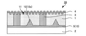
- the present invention relates to a hologram layer on which a hologram is recorded, a stress light emitting layer formed in a pattern on at least one surface side of the hologram layer, and containing stress light emitting particles and a binder resin; And a filling layer formed on the same plane.
- the presence of the stress light-emitting layer can be concealed by having the above-mentioned filling layer.
- the hologram sheet can be made to emit light in a pattern while concealing that the stress light-emitting layer is formed in a pattern.
- the hologram sheet of the present invention has a surface on which the stress luminescent layer is disposed by providing a filling layer between the patterns.
- a hologram layer on one surface side of the stress light emitting layer.
- the hologram layer is thin, like a relief hologram layer, and changes its shape during manufacturing. Even if it is easy to form, it is easy to form because the formation surface is made flat by the pattern-like stress emission layer and the filling layer.
- the color of the filling layer is similar to the color of the stress light emitting layer. This is because the presence of the stress-stimulated light emitting layer formed in a pattern can be effectively concealed, and the hologram sheet can be made more excellent in the anti-counterfeit effect.
- a concealing layer which is formed on at least one surface side of the stress-stimulated luminescent layer and conceals the presence of the stress-stimulated luminescent layer. This is because the presence of the stress-stimulated light emitting layer formed in a pattern can be effectively concealed, and the hologram sheet can be made more excellent in the anti-counterfeit effect.
- the present inventors have formed a stress concentration portion, which is a portion where stress is concentrated on a layer containing stress luminescent particles, so that the stress concentration portion can be reduced.
- the present inventors have found that the emission intensity can be increased at the formed position, and have completed the present invention.
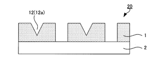
- the present invention has a stress-stimulated luminescent layer containing stress-stimulated luminescent particles and a binder resin, and a stress concentration portion including at least one of a concave portion and a convex portion is formed on at least one of the surface and the side surface of the stress-stimulated luminescent layer.
- a stress-stimulated luminescent sheet There is provided a stress-stimulated luminescent sheet.
- the stress concentration portion is formed in the stress light emitting layer, when stress is applied to the stress light emitting sheet, the stress can be concentrated on the stress concentration portion of the stress light emission layer. For this reason, the stress light emitting layer can emit light efficiently at the place where the stress concentration portion is formed. Therefore, the stress-stimulated luminescent sheet can be made excellent in the forgery prevention effect.
- a coating resin layer covering the stress concentration portion is formed. This is because stress can be effectively concentrated on the stress concentration portion when stress is applied to the stress light-emitting sheet.
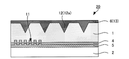
- a relief hologram is recorded on the surface of the stress-stimulated luminescent layer where the stress concentration portion is not formed. It is possible to prevent forgery by light emission from the stress light emitting layer and a relief hologram recorded in the stress light emitting layer. In addition, the hologram image recorded in the stress light emitting layer can be reproduced by light emission from the stress light emitting layer. For this reason, it is because a stress light-emitting sheet can be made more excellent in the forgery prevention effect.
- a hologram layer formed on at least one surface side of the stress-stimulated luminescent layer and on which a hologram is recorded. It is possible to prevent forgery by the light emitted from the stress light emitting layer and the hologram recorded on the hologram layer. Further, the hologram image recorded on the hologram layer by the light emission from the stress light emitting layer can be reproduced. For this reason, it is because a stress light-emitting sheet can be made more excellent in the forgery prevention effect.
- the present inventors have used a thread base material having a stress light emitting layer as a thread base material embedded in a paper layer.
- the inventors have found that authenticity can be easily determined, and have completed the present invention.
- the present invention has a paper layer and a belt-like thread base material embedded in the paper layer and embedded on at least one surface of the paper layer.
- the thread base material has a stress light emitting layer containing stress light emitting particles and a binder resin, the stress light emitting layer is formed in a pattern, and the thread base material is formed.
- the thread base material since the thread base material has the stress light emitting layer, the thread base material can emit light when stress is applied to the anti-counterfeit paper. For this reason, it is possible to determine the authenticity using light emitted from the stress light emitting layer even in a dark place. Further, at least one surface of the paper layer is formed with an opening in which a part of the thread base material is exposed in plan view, and the thread base material is exposed in the pattern of the opening, When stress is applied to the anti-counterfeit paper, the area in which the thread base material is embedded can emit light in a pattern shape in which the opening is formed.
- the thread base material is embedded and embedded in the paper layer, it is possible to easily form an opening in which a part of the thread base material is exposed in plan view. Therefore, it is easy to determine the authenticity even in a dark place, and it is possible to easily form an anti-counterfeit paper having an excellent anti-counterfeit effect.
- the stress light emitting layer is formed in a pattern, the stress light emitting layer can emit light in a pattern when stress is applied to the forgery prevention paper. Furthermore, the presence of the stress-stimulated luminescent layer formed in a pattern can be concealed, and the anti-counterfeit paper can be made more excellent in the anti-counterfeit effect.
- a relief hologram is recorded in the stress-stimulated luminescent layer. It is possible to prevent forgery by light emission from the stress light emitting layer and a relief hologram recorded in the stress light emitting layer. In addition, the hologram image recorded in the stress light emitting layer can be reproduced by light emission from the stress light emitting layer. For this reason, it is because a forgery prevention paper can be made excellent by the forgery prevention effect.
- the thread base material has a hologram layer on which a hologram is recorded. It is possible to prevent forgery by light emission from the stress light emitting layer and a relief hologram recorded on the hologram layer. Further, the hologram image recorded on the hologram layer by the light emission from the stress light emitting layer can be reproduced. For this reason, it is because a forgery prevention paper can be made excellent by the forgery prevention effect.
- the present invention produces an effect that a hologram sheet excellent in the forgery prevention effect can be provided.
- FIG. 5 is a sectional view taken along line AA in FIG. 4.
- FIG. 8 is a sectional view taken along line BB in FIG.
- FIG. 13 is a sectional view taken along line DD of FIG.
- FIG. 13 is a sectional view taken along line DD of FIG.
- FIG. 13 is a sectional view taken along line DD of FIG.
- FIG. 13 is a sectional view taken along line DD of FIG.
- FIG. 13 is a sectional view taken along line DD of FIG.
- FIG. 13 is a sectional view taken along line DD of FIG.
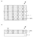
- FIG. 13 is a schematic plan view which shows an example of the hologram sheet of this invention.
- FIG. 34 is a cross-sectional view taken along line LL in FIG. 33. It is the schematic plan view and sectional drawing which show the other example of the stress light emission sheet
- FIG. 37 is a sectional view taken along line NN in FIG. 36.
- FIG. 37 is a sectional view taken along line OO in FIG. 36.
- FIG. 43 is a sectional view taken along line PP in FIG. 42. It is a schematic plan view which shows the other example of the thread
- FIG. 45 is a cross-sectional view taken along the line QQ in FIG. 44.
- It is a schematic sectional drawing which shows the other example of the thread
- FIG. 50 is a cross-sectional view taken along line RR in FIG. 49. It is a schematic sectional drawing which shows the other example of the thread
- FIG. 55 is a sectional view taken along line SS of FIG. 54.
- FIG. 55 is a cross-sectional view taken along line TT in FIG. 54. It is the schematic plan view and sectional drawing which show the other example of the forgery prevention paper of this invention.
- the hologram sheet of the present invention has a stress luminescent layer containing stress luminescent particles and a binder resin, and a mode in which a relief hologram is recorded in the stress luminescent layer (first embodiment) and stress luminescence A mode in which the layer has a hologram layer in which a hologram is recorded, and a filling layer formed in a pattern on at least one surface side of the hologram layer and formed on the same plane as the stress light emitting layer (second Embodiment) and two embodiments.
- first embodiment stress luminescent layer
- stress luminescence A mode in which the layer has a hologram layer in which a hologram is recorded, and a filling layer formed in a pattern on at least one surface side of the hologram layer and formed on the same plane as the stress light emitting layer (second Embodiment) and two embodiments.
- the hologram sheet of the present invention will be described separately for each embodiment.
- the hologram sheet of this aspect has a stress light emitting layer containing stress light emitting particles and a binder resin, and a relief hologram is recorded on the stress light emitting layer.
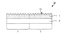
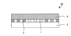
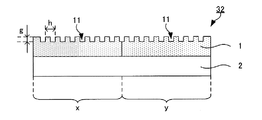
- FIG. 1 is a schematic cross-sectional view showing an example of the hologram sheet of this aspect.
- the hologram sheet 10 of this embodiment has a stress luminescent layer 1 containing stress luminescent particles and a binder resin, and a relief hologram is recorded on the stress luminescent layer 1.
- the stress luminescent layer 1 is formed on one surface of the substrate 2, and the surface on which the uneven relief 11 of the stress luminescent layer 1 is formed is the stress luminescent layer 1. This is the surface opposite to the side on which the substrate 2 is formed, and the deposited layer is not formed on the formation surface of the relief 11 of the stress light emitting layer 1.
- the relief hologram is recorded in the stress-stimulated luminescent layer containing the stress-stimulated luminescent particles and the binder resin, so that the forgery prevention by the hologram and the forgery prevention by the light emission can be achieved, and the forgery prevention effect of the hologram sheet. It can be made excellent. For this reason, for example, it is possible to reproduce a hologram image recorded in the stress light emitting layer by applying stress to the stress light emitting layer at night or the like.
- the relief hologram is recorded on the surface of the stress light-emitting layer, for example, the light emission of the stress light-emitting layer directly reaches the uneven relief compared to the case where the hologram layer and the stress light-emitting layer are formed separately.
- the relief hologram can be reproduced with higher definition. Therefore, by using the stress light emitting layer, forgery prevention by hologram and forgery prevention by light emission can be achieved, and the hologram sheet can be excellent in forgery prevention effect.
- the relief hologram is recorded in the stress light emitting layer containing the stress light emitting particles and the binder resin, for example, the step of laminating both layers after forming the hologram layer and the stress light emitting layer separately. It can be unnecessary. For this reason, it can be set as a hologram sheet with easy formation.
- the hologram sheet of this aspect has a stress light emitting layer.
- each structure in the hologram sheet of this aspect is demonstrated.
- Stress-stimulated layer The stress-stimulated layer in this embodiment has a relief hologram recorded thereon.
- the stress-stimulated luminescent layer contains stress-stimulated luminescent particles and a binder resin.
- the stress-stimulated luminescent layer contains stress-stimulated luminescent particles and a binder resin.
- Stress-stimulated luminescent particles have a property that the particles themselves emit light by strain energy applied from the outside, and a property that changes the luminescence intensity in proportion to the strain energy. Anything is acceptable.
- the wavelength of light emitted from the stress-stimulated luminescent particles (hereinafter sometimes referred to as a predetermined wavelength) is included in the range of visible light.
- the visible light wavelength range may be in the range of 400 nm to 800 nm.
- the said predetermined wavelength shall have area
- the predetermined wavelength refers to the maximum peak wavelength of the emission spectrum of stress-stimulated luminescent particles within a wavelength range of 200 nm to 1000 nm.
- the emission luminance of the stress luminescent particles is preferably 1.0mcd / cm 2 or more, among others, are 10mcd / cm 2 or more In particular, it is preferably 100 mcd / cm 2 or more. This is because when the emission luminance is within the above range, it can be recognized as high luminance outdoors, and the reliability of authenticity determination using emission from the stress emission layer can be improved.
- fluorescent light-emitting material examples include strontium aluminate added with europium as the emission center (SrAl 2 O 4 : Eu, green emission), zinc sulfide added with manganese as the emission center (ZnS: Mn, emission in yellow green) Etc.
- the type of stress-stimulated luminescent material constituting the stress-stimulated luminescent particles is not limited to one using only one type, and two or more types may be used. In this embodiment, it is preferable that there are two or more kinds of the stress-stimulated luminescent materials.
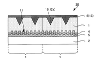
- the stress-stimulated luminescent layer can have regions with different luminescent colors. For example, for the stress-stimulated luminescent layer 1 in FIG. 2, the region indicated by x is the first luminescent color region containing the stress-stimulated luminescent particles made of the first stress luminescent material, and the region indicated by y is the second stress.
- the hologram sheet can be made excellent in the effect of preventing forgery. Further, when two or more stress-stimulated luminescent layers are stacked on the same hologram sheet, the types of stress-stimulated luminescent particles contained in the stress-stimulated luminescent layers may be the same or different. Note that the reference numerals in FIG. 2 indicate the same members as those in FIG. 1, and a description thereof will be omitted here.
- a mixture of stress-stimulated luminescent particles made of each stress-stimulated luminescent material for example, the luminescent color from the first stress-stimulated luminescent particles and the second A stress-stimulated luminescent layer of one luminescent color in which luminescent colors from stress-stimulated luminescent particles are mixed may be used.
- the shape of the stress-stimulated luminescent particles can be a conventionally known shape.
- Examples of the shape include a substantially spherical shape, a spheroid shape, a polyhedron shape, a scale shape, a disk shape, a fiber shape, and a needle shape.
- the surface of the stress-stimulated luminescent particle has a fine uneven shape formed randomly. This is because the stress can easily be transmitted to the portion where the fine unevenness of the stress-stimulated luminescent particles is formed, and the stress-stimulated luminescent particles can efficiently emit light.
- the concavo-convex shape may have a concavo-convex period and depth of nano size to several micrometers.
- the average primary particle diameter of the stress-stimulated luminescent particles is not particularly limited as long as a stress-stimulated luminescent layer having a desired luminescence intensity can be obtained. Is preferred. It is because it can be set as the stress light emitting layer excellent in emitted light intensity by being the said particle size.
- the average primary particle size can be determined by a method of measuring using a laser diffraction scattering method.
- the laser diffraction / scattering method uses a diffraction / scattering phenomenon of light by uniformly dispersing particles in a dispersion medium and then irradiating the particles with laser light.
- the intensity pattern of the diffraction / scattered light is Depending on the size of the particle, different intensity patterns (intensity distributions) are observed depending on the angle of diffraction / scattered light, and the particle size distribution is obtained using the Franhofer diffraction theory or Mie scattering theory. .
- the average primary particle size is determined using a laser diffraction / scattering method, it can be measured either dry or wet. When measuring by wet, water or ethanol can be measured as a dispersion.
- a laser beam used for a laser diffraction scattering method a semiconductor laser (wavelength 680 nm) etc. can be used as a laser beam used for a laser diffraction scattering method.
- the stress-stimulated luminescent particles are preferably coated with a water-resistant coating formed using a water-resistant material for improving water resistance. This is because it is possible to prevent the collapse of the crystal structure of the stress-stimulated luminescent material and the loss of luminescent property due to water. Further, the water resistance and weather resistance of the hologram sheet can be improved.
- a stress-stimulated luminescent layer or a hologram sheet including a stress-stimulated luminescent layer that has been subjected to a predetermined adjustment is used. The method of performing the test can be used. In the above JIS standard, the water immersion test is carried out for 4 hours.
- the improvement in water resistance means that the half time of a stress luminescent layer using a stress luminescent particle formed with a water-resistant coating and the stress luminescent layer using a stress luminescent particle not formed with a water-resistant coating It means that the half time is 2.0 times or more by comparing with the half time.
- the target half-life is preferably 2.0 times or more and 10 times or less.
- the water resistant material is not particularly limited as long as it can improve the water resistance of the stress-stimulated luminescent particles.
- silane coupling agent for example, silane coupling agent, thermoplastic resin, thermosetting resin, metal alkoxide, metal oxidation And the like.
- thermoplastic resin for example, polyethylene glycol dimethacrylate
- thermosetting resin for example, polypropylene glycol dimethacrylate
- metal alkoxide for example, polystyrene, polystyrene, polystyrene, polystyrene, polymethyl methacrylate, polymethyl methacrylate, polymethyl methacrylate, polymethyl methacrylate, polymethyl methacrylate, polymethyl methacrylate, polymethyl methacrylate, polymethyl methacrylate, polymethyl methacrylate, polymethyl methacrylate, polymethyl methacrylate, polymethyl methacrylate, polymethyl methacrylate, polymethyl methacrylate, polysulfate, polysulfate, polysul
- the silane coupling agent is not particularly limited as long as it can improve the water resistance of the stress-stimulated luminescent particles, but those having a vinyl group such as vinyltrimethoxysilane and vinyltriethoxysilane, 3- Those having an epoxy group such as glycidoxypropylmethyldimethoxysilane, those having a styryl group such as P-styryltrimethoxysilane, those having an acrylic group such as 3-acryloxypropyltrimethoxysilane, etc.
- 3-methacryloxypropyltrimethoxysilane Those having a methacrylic group such as 3-isocyanate propyltriethoxysilane having an isocyanate group, trimethylsilylchlorolide, hexamethyldisilazane, BSTFA (N, O-bis-trimethylsilyl-trifluoroacetamide) Triethylsilyl chloride, chloromethyltrimethylsilane, trimethylsilylacetylene, mention may be made of hexamethyldisilane, N, a N'- bis trimethylsilyl urea.
- the thermoplastic resin is not particularly limited as long as it can improve the water resistance of the stress-stimulated luminescent particles.
- polymethyl methacrylate, polymethyl acrylate, polybenzyl methacrylate, polybutyl acrylate, polyisobutyl Acrylate ester resins such as acrylate, cellulose resins such as cellulose nitrate, methyl cellulose, ethyl cellulose, and cellulose acetate propionate
- vinyl resins such as polyvinyl acetate and polyvinyl chloride-vinyl acetate copolymer, acrylamide resins, and polystyrene Examples thereof include resins.
- thermosetting resin is not particularly limited as long as it can improve the water resistance of the stress-stimulated luminescent particles.
- unsaturated polyester resin acrylic urethane resin, epoxy-modified acrylic resin, melamine resin
- examples include epoxy-modified unsaturated polyester resins, alkyd resins, phenol resins, silicone resins, and fluorinated resins.
- metal element constituting the metal alkoxide examples include aluminum, zirconium, titanium, and silicon.
- alkoxide methoxide, ethoxide, propoxide, isopropoxide, oxyisopropoxide, butoxide and the like can be used.
- Specific examples of the metal alkoxide include ethyl silicate and methyl silicate obtained by partially hydrolyzing and condensing tetraethoxysilane or tetramethoxysilane.
- the metal alkoxide is preferably tetraethoxysilane, tetramethoxysilane, tetraethyl silicate, tetramethyl silicate, aluminum triisopropoxide, zirconium tetraisopropoxide, titanium tetraisopropoxide, or the like. This is because the stress-stimulated luminescent particles can be excellent in water resistance.
- Examples of the metal oxide include alumina and titanium dioxide.
- the thickness of the water-resistant film is not particularly limited as long as the desired water resistance can be obtained.
- the thickness can be in the range of 0.1 ⁇ m to 10 ⁇ m.
- the method for forming the water-resistant coating is not particularly limited as long as it is a method capable of accurately forming a water-resistant coating covering the surface of the stress luminescent particles.
- a method of drying and removing a solvent or the like as necessary after mixing the water-resistant material and the stress luminescent particles can be used.
- the mixing of the water resistant material and the stress-stimulated luminescent particles may be performed in an organic solvent.
- a chemical vapor deposition method when the water-resistant material is a metal oxide, a chemical vapor deposition method (CVD method or the like) can be used.
- organic solvent examples include alcohol solvents such as ethyl alcohol, propyl alcohol, and butyl alcohol, ketone solvents such as acetone and methyl ethyl ketone, aromatic hydrocarbon solvents such as toluene, xylene, and benzene, methyl cellosolve, and ethyl cellosolve.
- alcohol solvents such as ethyl alcohol, propyl alcohol, and butyl alcohol
- ketone solvents such as acetone and methyl ethyl ketone
- aromatic hydrocarbon solvents such as toluene, xylene, and benzene, methyl cellosolve, and ethyl cellosolve.
- Glycol ether solvents such as propylcellsolve and butylcellsolve, diethylene glycol, triethylene glycol, polyethylene glycol, dipropylene glycol, tripropylene glycol, polypropylene glycol and other oxyethylene, oxypropylene addition polymers, ethylene glycol, propylene glycol Alkylene glycol such as 1,2,6-hexanetriol, glycerin, 2-pyrrolidone and the like can be preferably used.
- System solvent can be preferably used ketone-based solvents.
- the water content of the organic solvent is not particularly limited as long as the water-resistant coating can be applied to the stress-stimulated luminescent particles, but it is preferably less than 0.5% by mass. This is because it is possible to suppress a decrease in light emission characteristics of the stress-stimulated luminescent particles due to moisture in the organic solvent.
- the content of the stress-stimulated luminescent particles is not particularly limited as long as a stress-stimulated luminescent layer having a desired luminescence intensity can be obtained, but it is in the range of 1 to 50% by mass in the stress-stimulated luminescent layer. It is preferable to be within. It is because it can be set as the stress light emitting layer excellent in emitted light intensity because the said content is in the above-mentioned range.
- the content of the stress-stimulated luminescent particles may be one type, that is, the content of the stress-stimulated luminescent particles may be uniform in the stress-stimulated luminescent layer. It is preferable that the light emitting layer has a portion having a different content of the upper stress luminescent particles. This is because the hologram sheet can be excellent in the forgery prevention effect by having the stress light emitting layer having regions with different light emission intensities. More specifically, the stress-stimulated luminescent layer 1 in FIG. 2 described above can have different contents of stress-stimulated luminescent particles in the region indicated by x and the region indicated by y. Further, when two or more stress-stimulated luminescent layers are laminated on the same hologram sheet, the types of content of the stress-stimulated luminescent particles in the stress-stimulated luminescent layers may be the same or different.
- any method that can form stress-stimulated luminescent particles having a desired shape may be used.
- the above-described forming method includes baking a stress-stimulated luminescent material composition containing components constituting the stress-stimulated luminescent material to form a sheet-like stress-stimulated luminescent material, and then pulverizing and classifying the luminescent particles. The method of obtaining can be used.
- Examples of the method of pulverizing the sheet-like stress luminescent material include a method using a pulverizer such as a ball mill, a rod mill, an autogenous pulverizing mill, a SAG (semi-autogenous pulverizing) mill, a high-pressure pulverizing roll, and a vertical axis impactor (VSI) mill. it can.
- the pulverization method is a method using a vertical impactor (VSI) mill. This is because the shape of the stress-stimulated luminescent particles tends to be complicated, and a rough uneven shape is easily formed on the surface of the stress-stimulated luminescent particles.
- the vertical impactor (VSI) mill is a fine pulverizer that rotates impact teeth at high speed and pulverizes the raw material by impact force.
- a rotary disk having a diameter of 100 mm to 1000 mm is rotated at 500 rpm to 10000 rpm. What rotates at high speed can be used.
- the method generally used for formation of a stress luminescent material can be used.
- Binder resin As the binder resin, the stress-stimulated luminescent particles can be stably dispersed and fixed, the light emitted from the stress-stimulated luminescent particles can be transmitted, and a relief hologram can be recorded.
- a thermoplastic resin, a thermosetting resin, and an ionizing radiation curable resin can be used.
- thermoplastic resin and the thermosetting resin for example, the same resins as the thermoplastic resin and the thermosetting resin described in the section “(a) Stress luminescent particles” can be used.
- the thermoplastic resin and thermosetting resin used are those copolymerized with silicon resin, fluorine-containing resin, etc., and those in which siloxane bonds or fluorine atoms are introduced into the molecules of the thermoplastic resin and thermosetting resin. be able to.
- the said thermoplastic resin and thermosetting resin can use 1 type, or 2 or more types, Furthermore, you may bridge
- thermoplastic resin and the thermosetting resin contain various curing catalysts, for example, a metal soap such as cobalt naphthenate or zinc naphthenate, or benzoyl peroxide for initiating polymerization with heat or ultraviolet rays, Peroxides such as methyl ethyl ketone peroxide, benzophenone, acetophenone, anthraquinone, naphthoquinone, azobisisobutyronitrile, or diphenyl sulfide may be blended.
- a metal soap such as cobalt naphthenate or zinc naphthenate
- benzoyl peroxide for initiating polymerization with heat or ultraviolet rays
- Peroxides such as methyl ethyl ketone peroxide, benzophenone, acetophenone, anthraquinone, naphthoquinone, azobisisobutyronitrile, or diphenyl sulfide may be blended.
- the ionizing radiation curable resin examples include epoxy acrylate, urethane acrylate, and acrylic-modified polyester.
- the ionizing radiation curable resin may be used by blending a monofunctional monomer, a polyfunctional monomer, an oligomer, or the like for the purpose of introducing a crosslinked structure or adjusting the viscosity.
- the said binder resin may use only 1 type, and may be used combining 2 or more types.
- the binder resin may include, for example, a first binder resin disposed so as to cover the stress luminescent particles and a second binder resin that disperses the stress luminescent particles covered with the first binder resin. .
- the refractive index difference between the binder resin and the stress-stimulated luminescent particles is not particularly limited as long as the binder resin can transmit light emitted from the stress-stimulated luminescent particles, but is preferably 0.3 or less. Of these, 0.1 or less is preferable.
- the refractive index difference is within the above range, the reflectance of the emitted light from the stress-stimulated luminescent particles at the interface between the binder resin and the stress-stimulated luminescent particles can be reduced. This is because the stress-stimulated luminescent layer can efficiently transmit light emitted from the stress-stimulated luminescent particles.
- the refractive index difference between the said 1st binder resin and 2nd binder resin is also small. This is because the reflectance of the emitted light from the stress luminescent particles at the interface between the first binder resin and the second binder resin can be reduced.
- the refractive index difference between the first binder resin and the second binder resin can be the same as the refractive index difference between the binder resin and the stress luminescent particle refractive index.
- the volume elastic modulus of the binder resin is preferably larger than the volume elastic modulus of the stress-stimulated luminescent particles. This is because, when stress is applied to the hologram sheet, the deformation applied to the stress light emitting layer can be effectively transmitted to the stress light emitting particles, and the stress light emitting layer can be made excellent in light emission efficiency.
- the stress-stimulated luminescent layer has stress-stimulated luminescent particles and a binder resin, but may contain other materials as necessary.
- the other materials include colorants such as pigments, additives such as curing accelerators, lubricants and auxiliaries.
- the binder resin is a thermoplastic resin or a thermosetting resin
- the other material can include silicon resin, fluorine-containing resin, silicon oil, silicon powder fine particles, and fluorine powder fine particles.
- a tetrafluorinated resin as a fully fluorinated resin, a trifluorinated resin as a partially fluorinated resin, polyvinylidene fluoride, polyvinyl fluoride, a perfluoroalkoxy fluororesin as a fluorinated resin copolymer, and a tetrafluoride resin.
- An ethylene-hexafluoropropylene copolymer, an ethylene-tetrafluoroethylene copolymer, an ethylene-chlorotrifluoroethylene copolymer, or the like can be used.
- content of said other material can be adjusted within the range which can permeate
- the stress-stimulated luminescent layer in this embodiment has a relief hologram recorded thereon and has a relief on the surface.
- the depth of the relief of the unevenness that is, the distance between the bottom of the adjacent recess and the top of the projection is not particularly limited as long as a desired relief hologram image can be recorded. About 0.01 ⁇ m.
- the pitch of the concave and convex reliefs that is, the period between the bottoms of adjacent concave portions or the top portions of adjacent convex portions is not particularly limited as long as a desired relief hologram image can be recorded. However, it can be, for example, around 1.0 ⁇ m.
- the depth of the relief of the unevenness is specifically indicated by g in FIG. 1, and the pitch of the relief of the unevenness is specifically indicated by h in FIG. is there.
- the recording surface of the relief hologram of the stress-stimulated luminescent layer that is, the surface on which the relief is formed is usually only on one surface of the stress-stimulated luminescent layer.
- the recording location in the stress luminescent layer of the relief hologram may be, for example, the entire surface of the stress luminescent layer or a part of the stress luminescent layer.
- the relief hologram recording surface may include at least one surface of the two or more stress-stimulated layers. It may include the surfaces of all the stress-stimulated luminescent layers above the layer.
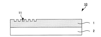
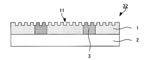
- FIG. 3 is a schematic cross-sectional view showing another example of the hologram sheet of this embodiment.
- FIG. 1 which has already been described shows an example in which the recording portion of the relief hologram is the entire surface of the stress-emitting layer, and
- FIG. 3 shows an example in which the recording portion of the relief hologram is a partial region of the stress-emitting layer. Note that the reference numerals in FIG. 3 indicate the same members as those in FIG.
- the type of relief hologram recorded on the stress-stimulated luminescent layer is only one type, that is, the relief hologram recorded on the stress-stimulated luminescent layer may show one image, but two or more types are included, That is, the relief hologram recorded on the stress light emitting layer may show two or more images.
- different types of relief holograms can be recorded in the area indicated by x and the area indicated by y in FIG.
- the types of relief holograms recorded on each stress-luminescent layer may be the same or different.
- the method for recording a relief hologram on the stress-stimulated luminescent layer is not particularly limited as long as it is a method capable of forming an uneven relief capable of reproducing a desired hologram image, and a conventionally known method can be used.
- a conventionally known method can be used.
- an original plate on which diffraction fringes or hologram interference fringes are recorded in a concavo-convex shape is used as a press mold, and the original plate is overlaid on a layer for forming a stress light emitting layer containing the stress light emitting particles and a binder resin.
- a method of forming a stress-stimulated luminescent layer having an uneven relief on the surface by transferring the concavo-convex relief of the original plate to the surface of the layer for forming the stress-stimulated luminescent layer by heating and pressure-bonding them by appropriate means such as a heating roll.
- the recording portion of the relief hologram includes the surface of the filling layer
- the above-described recording method is performed by superimposing the original on the stress emission layer forming layer and the filling layer forming layer formed on the same plane.
- a method such as thermocompression bonding can be used.
- the stress-stimulated luminescent layer is not formed in a pattern, that is, when the stress-stimulated luminescent layer is formed on the substrate, the stress-stimulated luminescent layer is formed so as to cover the entire surface of the substrate. However, it is preferably formed in a pattern.
- the stress light emitting layer By forming the stress light emitting layer in a pattern, the stress light emitting layer can emit light in a pattern in plan view when stress is applied to the hologram sheet. For this reason, it is because the hologram sheet can be made excellent in the forgery prevention effect because the stress-stimulated luminescent layer is formed in a pattern.
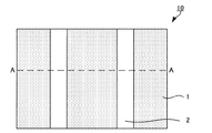
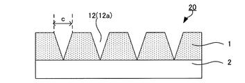
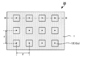
- FIG. 4 is a schematic plan view showing another example of the hologram sheet of this aspect.
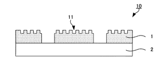
- FIG. 5 is a cross-sectional view taken along line AA in FIG.
- FIG. 1 already described shows an example in which the stress-stimulated luminescent layer 1 is formed on the entire surface of the substrate 2, and FIGS. 4 and 5 show examples in which the stress-stimulated luminescent layer 1 is formed in a pattern.
- FIGS. 4 and 5 show examples in which the stress-stimulated luminescent layer 1 is formed in a pattern.
- FIGS. 4 and 5 show the same members as those in FIG. 1, and the description thereof is omitted here.
- the shape of the stress-stimulated luminescent layer in plan view can be appropriately set according to the type and application of the hologram sheet of this aspect.
- the planar view shape of the stress light emitting layer can be a dot shape, a line shape, or the like.
- the planar view shape of the dot-like stress light-emitting layer can be an arbitrary shape such as a circular shape or a square shape.
- the planar view shape of the stress light emitting layer may represent a symbol, a character, or the like.
- the shape of the stress-stimulated luminescent layer in plan view may be, for example, a character using a line-shaped stress luminescent layer, or a character using a dot-like stress luminescent layer. Moreover, it may represent predetermined information using characters or the like. Further, when two or more stress luminescent layers are included in the same hologram sheet, the shape of each stress luminescent layer in plan view may be the same or different. 4 and 5 which have already been described show examples in the case where the stress emission layer 1 has a line shape in plan view.
- the width of the stress-stimulated luminescent layer is not particularly limited as long as a relief hologram can be recorded and light can be emitted in a desired pattern shape. Rather, it is appropriately set according to the type and use of the hologram sheet of this embodiment.
- the thickness of the stress-stimulated luminescent layer is not particularly limited as long as it is a stress-stimulated luminescent layer having a desired luminescence intensity and can record a desired relief hologram image, but is usually 0.1 ⁇ m to 6 ⁇ m. It can be in the range, and in particular, it is preferably in the range of 0.1 ⁇ m to 4 ⁇ m.
- the stress-stimulated luminescent layer is preferably transparent to predetermined light emitted from the stress-stimulated luminescent particles. This is because it is easy to make the stress light emitting layer excellent in light emission intensity.
- a predetermined wavelength it means that there is transparency with respect to light of a predetermined wavelength ⁇ 1% wavelength range, and in particular, a wavelength of predetermined wavelength ⁇ 5% It is preferably transparent to the light in the region.
- the predetermined wavelength is 500 nm
- the predetermined wavelength range of ⁇ 1% means a wavelength range of 495 nm to 505 nm.
- the term “transparency” means that the transmittance of light in at least a predetermined wavelength range is 50% or more, and preferably 80% or more.
- the transmittance in a wavelength region other than light of a predetermined wavelength may be less than 50% or less. It is because the unexpectedness at the time of light emission can be improved and it is suitable.
- the stress light emitting layer is observed as black or black by including three colorants of R (red), G (green), and B (blue), and the stress light emitting particles emit light having a predetermined wavelength ⁇
- absorption wavelength distribution (absorption wavelength curve) of each color so as to ensure a transmittance of 50% or more only in the 1% wavelength region, external stress can be applied from the stress-stimulated luminescent layer considered to be black.
- the total light transmittance of the stress-stimulated luminescent layer is preferably 20% or more, and preferably 60% or more. It is more preferable that Here, the transmittance of the stress-stimulated luminescent layer can be measured by JIS K7361-1 (Plastic—Testing method of total light transmittance of transparent material).
- the number of the stress-stimulated luminescent layers formed may be one or more on one hologram sheet. However, the number of stress-stimulated luminescent layers is two or more. It may be a thing. It is possible to easily form different stress-stimulated luminescent layers such as the type and content of stress-stimulated luminescent particles and the planar shape of the stress-stimulated luminescent layer, and the hologram sheet can be excellent in anti-counterfeiting effects. is there. 2 and 5, the plurality of stress light emitting layers 1 formed on the same plane are regarded as one stress light emitting layer.
- the method for forming the stress-stimulated luminescent layer is not particularly limited as long as it includes stress-stimulated luminescent particles and a binder resin and can record a relief hologram.
- a stress luminescent ink is formed by dispersing or dissolving a stress luminescent particle and a binder resin, which are constituent materials of the stress luminescent layer, in a solvent, and applying the stress luminescent ink, and then applying the stress luminescent ink.
- a method of recording a relief hologram on a stress-luminescent layer forming layer after forming a stress-luminescent layer-forming layer by removing the solvent from the ink coating by drying Can be mentioned.
- the formation method of the layer for stress light emitting layer formation can use the method of apply
- the printing method is not particularly limited as long as it is a printing method capable of forming a stress-stimulated light emitting layer having a desired pattern shape.
- the printing method include spray printing and coating.
- solvent examples include cyclic hydrocarbons (cyclohexane, etc.), alcohols (methanol, ethanol, isopropyl alcohol, n-propyl alcohol, isobutyl alcohol, n-butyl alcohol, etc., and their aqueous solutions), ethers (tetrahydrofuran, methyl).
- cyclic hydrocarbons cyclohexane, etc.
- alcohols methanol, ethanol, isopropyl alcohol, n-propyl alcohol, isobutyl alcohol, n-butyl alcohol, etc.
- ethers tetrahydrofuran, methyl
- esters ethyl acetate, butyl acetate
- Isobutyl acetate propylene glycol monomethyl ether acetate
- cellosolve acetate can be mentioned ethyl-3-ethoxypropionate and the like
- water and / or lower alcohols such as methanol, ethanol, propanol, and butyl alcohol, glycols, and cell solves can be used as the solvent.
- the method of forming the stress-stimulated luminescent ink is not particularly limited as long as it is a method capable of stably dispersing or dissolving the stress-stimulated luminescent particles and the binder resin in the solvent.
- the binder resin is dispersed or dissolved in the solvent.
- An example is a method in which stress luminescent particles are added and stirred.
- the drying method is not particularly limited as long as the solvent can be sufficiently removed. Natural drying, contact heat drying at 40 ° C. to 80 ° C., hot air drying at 40 ° C. to 200 ° C., vacuum drying. Etc. can be used. In addition, as the drying method, ultraviolet ray irradiation, drying using a curing reaction by electron beam irradiation, or the like may be used alone or in combination.
- the hologram sheet of this aspect has a stress-stimulated luminescent layer, but may have other configurations as necessary.
- the hologram sheet of this aspect can include a substrate that supports the stress-stimulated luminescent layer. This is because the stress light emitting layer and the like can be easily formed by having the substrate. 1 to 5 already described show examples in which the hologram sheet has the substrate 2.
- the base material is a light-shielding base material having a light-shielding property with respect to light having a predetermined wavelength, even if the base material is transparent with respect to light having a predetermined wavelength emitted from the stress-luminescent particles.
- it is preferably a transparent substrate. This is because the light and the hologram image from the stress light emitting layer can be recognized on both sides of the hologram sheet.
- the total light transmittance of the substrate is preferably 80% or more, and more preferably 90% or more.
- the transmittance measurement method can be the same as the method described in the section “1. Stress light emitting layer”.
- the light emission of the stress light emitting layer can be observed only from the side of the hologram sheet where the stress light emitting layer is formed or from the end of the hologram sheet. Can be made excellent in anti-counterfeiting effect.
- the substrate include, for example, polyethylene film, polypropylene film, polyvinyl fluoride film, polyvinylidene fluoride film, polyvinyl chloride film, polyvinylidene chloride film, ethylene-vinyl alcohol copolymer film, polyvinyl alcohol film. , Polymethyl methacrylate film, polyether sulfone film, polyether ether ketone film, polyamide film, tetrafluoroethylene-perfluoroalkyl vinyl ether copolymer film, polyester film such as polyethylene terephthalate film, resin film such as polyimide film, etc. be able to.
- the thickness of the base material is appropriately selected according to the use and type of the hologram sheet of the present embodiment, but can be in the range of 2 ⁇ m to 200 ⁇ m, and in particular, in the range of 10 ⁇ m to 50 ⁇ m. Preferably there is. This is because it is easy to make the hologram sheet flexible.
- the ratio of the thickness of the base material to the thickness of the stress light emitting layer can be in the range of 1/10 to 30/10. When the thickness ratio is within the above-described range, the hologram sheet does not have too high rigidity, and the light-transmitting light from the stress-stimulated light-emitting layer is excellent. Further, the deformation stress of the hologram sheet is easily transmitted as the deformation stress of the stress light emitting layer.
- the base material is treated with, for example, corona treatment, ozone treatment, plasma treatment, ionizing radiation treatment, dichromate treatment, anchor on the surface of the base material.
- surface treatment such as primer treatment may be performed.
- primer agents such as urethane-based, acrylic-based, ethylene-vinyl acetate copolymer system, vinyl chloride-vinyl acetate copolymer system, etc. are known as the primer agent used by the above primer treatment. You can select and use one that matches the material.
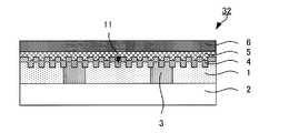
- the hologram sheet of this aspect can include a vapor deposition layer formed so as to be in contact with the uneven relief forming surface of the stress light emitting layer.
- a vapor deposition layer formed so as to be in contact with the uneven relief forming surface of the stress light emitting layer.
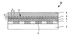
- FIG. 6 shows an example in which the deposited layer 4 is formed along the relief unevenness on the surface of the stress emitting layer 1 on which the uneven relief 11 is formed, and the unevenness derived from the uneven relief of the stress emitting layer 1 on the surface of the deposited layer 4.
- An example in which an interlayer adhesive layer 5 is formed so as to fill the structure is shown.
- FIG. 6 shows an example in which the surface on which the uneven relief 11 of the stress light emitting layer 1 is formed is on the substrate 2 side of the stress light emitting layer 1.
- the material constituting the vapor deposition layer is not particularly limited as long as it is a material that causes a difference in refractive index with the stress light emitting layer.
- Mg, Al, Ti, Cr, Fe, Co, Ni Metals such as Cu, Zn, Ga, Ge, Se, Rb, Pd, Ag, Cd, In, Sn, Sb, Te, Au, Pb, or Bi, oxides of these metals, or nitrides of these metals Can be used alone or in combination of these materials.
- the thickness of the vapor deposition layer can be appropriately set from the viewpoint of desired reflectivity, color tone, design, use, etc., and is preferably in the range of 50 to 1 ⁇ m, for example, in the range of 100 to 1000 ⁇ m. It is preferable. In addition, the thickness is preferably 200 mm or less from the viewpoint of providing transparency to the vapor deposition layer, and may be more than 200 mm from the viewpoint of providing concealment to the vapor deposition layer. preferable.
- a general vapor deposition layer formation method can be used, and examples thereof include a vacuum vapor deposition method, a sputtering method, and an ion plating method.
- the hologram sheet of this aspect can include a filling layer formed on the same plane as the stress-stimulated luminescent layer when the stress-stimulated luminescent layer is formed in a pattern. This is because the presence of the stress-stimulated luminescent layer formed in a pattern can be concealed, and the hologram sheet can be made more excellent in the anti-counterfeit effect.
- a hologram image recorded on the stress light emitting layer, pattern-like light emission from the stress light emitting layer, a pattern represented by the stress light emitting layer and the filling layer, etc. it can be made excellent in design. It is.
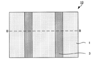
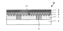
- FIG. 7 is a schematic cross-sectional view showing another example of the hologram sheet of this aspect.
- 8 is a cross-sectional view taken along line BB in FIG. 7 and 8 show an example in which the stress light emitting layer 1 is formed in a pattern and the hologram sheet 10 has a filling layer 3 formed on the same plane as the stress light emitting layer 1.
- the filling layer is formed on the same plane as the stress light emitting layer.
- being formed on the same plane means being formed on the same plane as the plane on which the stress light emitting layer is formed, and the portion where the stress light emitting layer is not formed in plan view. It means that it is formed.
- the filling layer is the same member as the stress light emitting layer so that both the stress light emitting layer and the filling layer are formed on the same surface of the substrate so as to be in contact with the substrate. On the same surface.
- the filling layer is used to conceal the presence of the stress-stimulated luminescent layer, and the formation of the filling layer makes the presence of the stress-stimulated luminescent layer less noticeable than before the formation of the filling layer.
- the color of the filling layer is not particularly limited as long as it can conceal the presence of the stress-stimulated luminescent layer, and may be monochromatic or multicolored. Furthermore, it is preferable that it is a single color from a viewpoint of making it the same color.
- the color of the filling layer is a single color, it is preferably the same color as that of the stress-stimulated luminescent layer, and in particular, the same color as that of the stress-stimulated luminescent layer. This is because the anti-counterfeiting effect can be improved, for example, the presence of the stress-stimulated light-emitting layer in which the color of the filling layer is formed in a pattern can be effectively concealed.
- the same color means that the color difference in the L * a * b * color system defined by JISZ8730 is 20 or less.
- the same color means that the color difference is within 0.5.
- the color of the stress-stimulated luminescent layer refers to the color when no light is emitted.
- the color of the filling layer may represent a pattern by the filling layer, and may be such that a region where the stress light emitting layer is formed is recognized as a part of the pattern. This is because it is possible to conceal the presence of the stress-stimulated luminescent layer formed in a pattern while being excellent in design.
- the constituent material of the filling layer is not particularly limited as long as it can form a filling layer of a desired color, but may contain a resin material. Moreover, the said constituent material shall contain a white pigment and another component as needed. In this embodiment, it is preferable to have a white pigment from the viewpoint that the color of the filling layer is the same color as the stress light emitting layer. Since the stress-stimulated luminescent particles contained in the stress-stimulated luminescent layer are generally white, having a white pigment makes it easy to make the color of the filling layer similar to the color of the stress-stimulated luminescent layer. This is because the presence of the light emitting layer can be effectively concealed.
- the white pigment is not particularly limited as long as it has a property of not emitting light even when stress is applied, and examples thereof include titanium dioxide, zinc white, and antimony trioxide.
- the particle size and content of the white pigment are not particularly limited as long as the color of the filling layer can be the same color as that of the stress light emitting layer.
- the particle diameter and content can be the same as the content of the particle diameter and content of the stress-luminescent particles described in the section “1.
- the resin material a general resin material can be used.
- Stress light emitting layer” can be used.
- the resin material is preferably the same as the binder resin contained in the stress light emitting layer from the viewpoint that the color of the filling layer is similar to the color of the stress light emitting layer. This is because it is easy to make the color of the filling layer similar to the color of the stress light emitting layer, and the presence of the stress light emitting layer can be effectively concealed.
- the other components include additives generally used together with resin materials, and the same materials as the other materials described in the above section “1. Stress light emitting layer” may be used. it can.
- the other components are preferably the same as other materials contained in the stress luminescent layer.
- the content ratio of the other components to the resin material is preferably the same as the content ratio of the other materials included in the stress light-emitting layer to the binder resin included in the stress light-emitting layer.
- the filler layer preferably contains the same colorant as the colorant contained in the stress-stimulated luminescent layer. It is preferable that the content ratio with respect to the resin material is the same as the content ratio of the colorant in the stress light emitting layer with respect to the binder resin. This is because it is easy to make the filling layer have the same color as the stress light emitting layer, and the presence of the stress light emitting layer can be effectively concealed.
- the total light transmittance of the filling layer is not particularly limited as long as the stress light emitting layer can be concealed.
- the transmittance can be the same as that described in the section “1. Stress light emitting layer”, for example.
- the color of the filling layer is the same color as that of the stress light emitting layer, it is preferably the same as the stress light emitting layer.
- the thickness of the filling layer is not particularly limited as long as the stress-stimulated luminescent layer can be concealed.
- the thickness can be the same as that described in the section “1.
- the thickness is preferably the same as the thickness of the stress luminescent layer. This is because it is easy to make the color of the filling layer similar to the color of the stress light emitting layer, and the presence of the stress light emitting layer can be effectively concealed.
- the formation place of the filling layer in plan view is not particularly limited as long as the stress light emitting layer is not formed, and includes, for example, all the places where the stress light emission layer is not formed. It may include a part of the portion where the stress light emitting layer is not formed. 7 and 8 which have already been described are formed so that the stress-stimulated luminescent layer and the filling layer are in direct contact with each other.
- the filling layer may have a relief hologram recorded on the surface. This is because the hologram sheet can be made more excellent in the effect of preventing forgery.
- FIG. 7 and FIG. 8 already described show examples in which relief holograms are recorded in both the filling layer and the stress light emitting layer. It should be noted that the depth and pitch of the uneven relief, the recording surface of the relief hologram, the recording location, the type of the relief hologram, the recording method of the relief hologram, and the like are the same as those described in the above section “1. Stress light emitting layer”. The description here is omitted.
- the filling layer may be formed for a part of the stress-stimulated luminescent layers. It is preferable to be formed. This is because the presence of the stress light emitting layer can be effectively concealed.
- the filling layer is formed on the same plane with respect to each of the two stress light emitting layers, and both of the two stress light emitting layers are formed by the filling layer. It is preferable to be concealed.
- the filling layer may be formed by any method that can stably form the filling layer on the same plane as the stress-stimulated luminescent layer.
- a method similar to the method of forming the stress-stimulated luminescent layer may be used. it can.
- the forming method for example, a method of preparing a filling layer by preparing a filling layer forming ink, forming a coating film of the filling layer forming ink using a printing method, and then drying the coating film, etc. Can be mentioned.
- the order of forming the stress-stimulated luminescent layer and the filling layer is not particularly limited, and any of them may be formed first or simultaneously.
- the hologram sheet of this aspect may include a hiding layer that is formed on at least one surface side of the stress-stimulated luminescent layer and hides the presence of the stress-stimulated luminescent layer.
- a concealing layer formed so as to cover the stress-stimulated luminescent layer, it becomes possible to effectively conceal the presence of the stress-stimulated luminescent layer formed in a pattern, etc. Because it can.
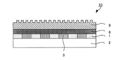
- FIG. 9 is a schematic cross-sectional view showing another example of the hologram sheet of this aspect.
- FIG. 9 shows an example in which the hologram sheet 10 has a concealing layer 6 formed on one surface side of the stress light emitting layer 1.
- the concealing layer conceals the presence of the stress light emitting layer.
- the concealing layer is formed on at least one surface side of the stress light emitting layer.
- the color of such a concealing layer is not particularly limited as long as it can conceal the presence of the stress-stimulated luminescent layer, and may be monochromatic or multicolored.
- the color of the concealing layer may be the same color as the color of the stress-stimulated luminescent layer or a non-similar color. For example, when the hologram sheet is viewed in plan, it is possible to reduce the color difference between the stress-stimulated luminescent layer formed in a pattern and the surrounding area, and the existence of the stress-stimulated luminescent layer is effective. This is because it can be concealed. In this embodiment, it is preferable that the color of the concealing layer is lighter than the color of the stress light emitting layer.
- the anti-counterfeiting effect can be improved, for example, the presence of the stress-stimulated light-emitting layer formed in a pattern can be effectively concealed.
- the color of the concealing layer is not similar to the color of the stress light emitting layer and the lightness is low, for example, when the stress light emitting layer is milky white, a purple concealing layer is used. Can be mentioned.
- the color of the concealment layer may represent a pattern by the concealment layer, and the stress light emitting layer formed in a pattern shape may be recognized as a part of the pattern. This is because it is possible to conceal the presence of the stress-stimulated luminescent layer formed in a pattern while being excellent in design.
- the constituent material of the concealment layer is not particularly limited as long as it can form a concealment layer of a desired color, but may include a resin material. Moreover, the said constituent material shall contain a white pigment and another component as needed.
- the resin material, the white pigment, and other components can be the same as those described in the section “(3) Packing layer”, and thus description thereof is omitted here.
- the concealing layer is not particularly limited as long as it can transmit the light emitted from the stress light emitting layer while concealing the stress light emitting layer.
- the total light transmittance of the concealment layer may be the same as the content described in the section “(3) Packing layer”, for example.
- the thickness of the concealment layer is not particularly limited as long as it can form a concealment layer of a desired color.
- the thickness is the same as the content described in the section “(3) Packing layer”. The description here is omitted.
- the formation location of the concealment layer in plan view may be any location as long as it includes a location overlapping the stress emission layer in plan view, and may include all of the locations where the stress emission layer is formed. A part of the portion where the stress-stimulated luminescent layer is formed may be included. Moreover, the formation location in the planar view may include both the location where the stress light emitting layer is formed and the location where the filling layer is formed.
- the formation position in the thickness direction of the concealing layer with respect to the stress light emitting layer may be formed on at least one surface side of the stress light emitting layer, and may be only one surface side of the stress light emitting layer, Both surface sides may be sufficient.
- the concealing layer may be formed so as to be in contact with the stress-stimulated light emitting layer, or may be formed via another layer.
- the concealing layer is formed only on one surface side of the stress light emitting layer, and is formed through another layer such as the stress light emitting layer and the filling layer and the interlayer adhesive layer.
- FIG. 9 shows an example where the concealed layer formation place in plan view includes all the places where the stress light emitting layer is formed and the place where the filling layer is formed.
- the other configurations described above can include those generally used for hologram sheets.
- an interlayer adhesive layer that bonds between the components such as the stress-stimulated luminescent layer and the substrate, an ultraviolet absorbing layer, a printed layer, a fluorescent material that can be excited by light emission from the stress-stimulated luminescent layer.
- a fluorescent layer a protective layer that protects the stress-emitting layer, an adhesive layer that is used to attach the hologram sheet to the adherend, a release sheet that is releasably attached on the surface of the adhesive layer, a stress-emitting layer, and a filling
- Examples thereof include a covering filling layer formed so as to cover the layer and formed integrally with the filling layer.
- the said interlayer adhesive bond layer may be provided in order to planarize the uneven
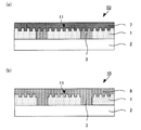
- FIG. 10A shows an example in which the hologram sheet 10 has a heat seal layer 7 as an adhesive layer formed so as to cover the stress light emitting layer 1 and the filling layer 3 having the same thickness as the stress light emitting layer 1. Is shown.
- FIG. 10B shows an example in which the hologram sheet 10 has a covering filling layer 8 formed so as to cover the stress light emitting layer 1 and the filling layer 3 and formed integrally with the filling layer 3. .
- the hologram sheet of this embodiment is excellent in scratch resistance, and the stress light emitting layer is hardly damaged when the hologram sheet is manufactured or used. it can.
- the covering filling layer can be easily formed by being formed integrally with the filling layer.
- the said other structure may serve as two or more types.
- FIG. 10A shows an example having the heat seal layer 7 as an adhesive layer, but the heat seal layer 7 in FIG. 10A is, for example, a concealment layer, a protective layer, a fluorescent layer, a print layer, etc. It may be used.
- 10B shows an example in which the covering filling layer 8 is used as a protective layer. However, the covering filling layer 8 in FIG. 10B is used as an adhesive layer such as a heat seal layer, a concealing layer, or the like. It may be done.
- the method for producing a hologram sheet of this aspect is not particularly limited as long as it is a method capable of producing a hologram sheet having the above-described configurations with high accuracy.
- a base material and a stress light emitting layer forming layer are laminated in this order, and then a hologram is recorded on the stress light emitting layer forming layer to form a stress light emitting layer.
- stacked in this order can be mentioned.
- the above manufacturing method is a method of obtaining a hologram sheet including only a stress light emitting layer by forming a laminate in which a base material and a stress light emitting layer are laminated in this order, and then peeling the base material from the laminate. May be.
- a hologram forming laminate in which a first base material and a stress emitting layer forming layer are laminated is prepared, and hologram recording is performed on the stress emitting layer forming layer of the hologram forming laminate. Then, the stress-stimulated luminescent layer is formed, and then the deposited layer is formed so as to cover the relief forming surface of the uneven surface of the stress-stimulated luminescent layer, and an adhesive is further applied on the deposited layer.
- a stress light emitting layer laminate in which a base material, a stress light emitting layer, a vapor deposition layer, and an interlayer adhesive layer are laminated in this order is formed, and then the second base material and the stress light emitting layer laminate are formed into a second
- the first substrate, the stress-stimulated luminescent layer, the vapor deposition layer, the interlayer adhesive layer, and the second substrate are arranged by placing the substrate and the interlayer adhesive layer so as to face each other and bringing the laminates into contact with each other.
- stacked in order can be mentioned.
- a method of obtaining a hologram sheet in which the second substrate, the interlayer adhesive layer, the vapor deposition layer, and the stress light emitting layer are laminated in this order by peeling the substrate may be used.
- the hologram sheet of this aspect it can be used for anti-counterfeiting purposes, and examples thereof include credit cards, cash cards and the like.
- the hologram sheet may have an adhesive layer that can adhere to another adherend, and may be used as a hologram sheet label that can be attached to the adherend.
- the hologram sheet may have a heat seal layer and may be used as a hologram sheet transfer foil that can be transferred to an adherend. Specifically, when the hologram sheet of this embodiment is used as a hologram sheet transfer foil and this is transferred to an adherend to form an anti-counterfeit medium, as illustrated in FIG.
- positioned so that the to-be-adhered body 101 and the heat-seal layer 7 may oppose the to-be-adhered body 101 can be mentioned.
- the constituent material of the heat seal layer can be the same as that generally used for the transfer foil, and for example, a heat-sensitive adhesive that melts or softens by heating and exhibits an adhesive effect can be preferably used.
- the heat sensitive adhesive include vinyl chloride resins, vinyl acetate resins, vinyl chloride vinyl acetate copolymer resins, acrylic resins, polyester resins, and the like.
- the adherend include those requiring anti-counterfeiting, and examples include those described as specific examples of a hologram sheet described later.
- FIG. 11 is a schematic plan view showing an example in which the forgery prevention medium is used as a bill
- FIG. 11B is a cross-sectional view taken along the line CC of FIG.
- the hologram sheet 10 has a structure in which a base material 2, a patterned light-emitting layer 1 and a filling layer 3, and a heat seal layer 7 are laminated in this order, and are attached via the heat seal layer 7. It is transferred to the body 101. Therefore, in FIG. 11, the hologram sheet 10 includes the base material 2 and the stress light emitting layer 1 included therein, the stress light emitting layer 1 is disposed on the adherend 101 side, and the base material 2 is the surface of the anti-counterfeit medium 100. It is arranged on the side.
- FIG. 11 shows an example in which the line-shaped stress-stimulated light-emitting layer 1 is formed in a pattern so as to represent the number “123”, and the forgery prevention medium 100 includes the printed layer 104 representing the number “500”. It is. Further, in FIG. 11A, the description of the base material is omitted for easy explanation.
- hologram sheet More specific uses of the hologram sheet include, for example, receivables, deposit certificates, receipts, bills, checks, bankbooks, magnetic forms, transfer cards, gift certificates, coupons, coupons, gifts, movie tickets, membership tickets, Securities such as beer vouchers and securities in the securities field, catalogs, flyers, brochures, leaflets, posters, POPs, greeting cards, postcards, stickers, invitations, reports, minutes, rosters , Name cards, business cards, participation certificates, manuals, company history, public relations magazines, in-house newsletters, fee schedules, transfer forms, purchase orders, production instructions, invoices, sales slips, etc.
- the above uses include driver's license, identification card such as employee ID card, membership card, admission ticket for entrance examination, passport, banknote, gift certificate, point card, stock certificate, lottery ticket, horse ticket, bankbook, If it is used forged, such as a ticket, a pass ticket, an air ticket, an admission ticket for various events, an amusement ticket, a cash voucher for transportation, etc., it may damage the holder of the securities or the issuing company. Things can be mentioned.
- high-priced products for example, high-grade watches, high-grade leather products, precious metal products, jewelry, etc. Examples include storage boxes and cases for expensive products.
- the hologram sheet of this aspect includes a hologram layer on which a hologram is recorded, a stress light emitting layer formed in a pattern on at least one surface side of the hologram layer, containing stress light emitting particles and a binder resin, and the stress light emitting layer. And a filling layer formed on the same plane.
- FIG. 12 is a schematic plan view showing an example of the hologram sheet of this aspect.
- 13 is a cross-sectional view taken along the line DD of FIG.
- the hologram sheet 10 of this aspect is formed in a pattern on the surface of at least one of the hologram layer 9 on which the hologram is recorded and the hologram layer 9. It has a stress light emitting layer 1 containing a resin and a filling layer 3 formed on the same plane as the stress light emitting layer 1.
- the hologram sheet 10 includes the base material 2, and the stress light emitting layer 1 and the filling layer 3 are formed on one surface of the base material 2. In addition, it is formed in the entire region where the stress light emitting layer 1 is not formed.
- the description of the hologram layer and the substrate is omitted for ease of explanation.
- the filling layer it becomes possible to conceal the presence of the stress-stimulated luminescent layer by having the filling layer.
- the color of the filling layer similar to the color of the stress light emitting layer, it is possible to conceal the presence of the stress light emitting layer formed in a pattern.
- the pattern is represented by a filling layer, and the region where the stress luminescent layer is formed is recognized as a part of the pattern, thereby concealing the presence of the stress luminescent layer formed in a pattern. can do.
- the hologram sheet can be made to emit light in a pattern while concealing that the stress light-emitting layer is formed in a pattern.
- the hologram sheet makes it possible to cause the stress light emitting layer to emit light in a pattern at night or the like, and to reproduce a hologram image recorded at a specific location of the hologram layer by the pattern light. For this reason, a stress-stimulated light-emitting layer that is concealed from being formed into a pattern, a hologram image recorded on the hologram layer by having a stress-stimulated light-emitting layer, a filling layer, and a hologram layer formed in a pattern
- the hologram sheet can be made excellent in anti-counterfeiting effect by combining the pattern-like light emission, the pattern represented by the stress light emitting layer and the filling layer.
- the design can be made excellent. Therefore, by having the stress-stimulated light emitting layer, the filling layer, and the hologram layer formed in a pattern shape, the anti-counterfeiting effect can be excellent, and the design can be excellent.
- the hologram sheet of this aspect has a surface on which the stress light emitting layer is disposed by providing a filling layer between the patterns. Is easy to smooth. For this reason, it becomes possible to easily provide another layer such as a hologram layer on one surface side of the stress light emitting layer.
- a hologram layer is formed on one surface of a stress-stimulated luminescent layer after forming a patterned stress-stimulated luminescent layer and a filling layer, the hologram layer is thin, like a relief hologram layer, and changes its shape during manufacturing. Even if it is easy to form, it is easy to form because the formation surface is made flat by the pattern-like stress emission layer and the filling layer.
- the hologram sheet of this embodiment has a hologram layer, a stress light emitting layer, and a filling layer.
- a stress light emitting layer has a hologram layer, a stress light emitting layer, and a filling layer.
- the stress light emitting layer in this embodiment is formed in a pattern on at least one surface side of the hologram layer.
- the stress-stimulated luminescent layer contains stress-stimulated luminescent particles and a binder resin.
- the stress-stimulated luminescent layer contains stress-stimulated luminescent particles and a binder resin.
- Stress-stimulated luminescent particles have a property that the particles themselves emit light by strain energy applied from the outside, and a property that changes the luminescence intensity in proportion to the strain energy. Anything is acceptable.
- the type of stress-stimulated luminescent material constituting the stress-stimulated luminescent particles is not limited to one using only one type, and two or more types may be used.
- the region indicated by x is the first luminescent color region containing stress-stimulated luminescent particles made of the first stress luminescent material
- the region indicated by can be a region of the second luminescent color containing stress-stimulated luminescent particles made of the second stress luminescent material.
- the content of the stress-stimulated luminescent particles may be one type, that is, the content of the stress-stimulated luminescent particles may be uniform in the stress-stimulated luminescent layer. It is preferable that a light emitting layer has a site
- Binder resin is not particularly limited as long as it can stably disperse and fix the stress-stimulated luminescent particles and transmit light emitted from the stress-stimulated luminescent particles.
- Examples of such a binder resin include those described in the section “(b) Binder resin” in “(1) Constituent material of stress luminescent layer” in “1. Since it can be the same as that of the contents, description thereof is omitted here.
- the stress-stimulated luminescent layer has stress-stimulated luminescent particles and a binder resin, but may contain other materials as necessary. Such other materials are described in the section “(c) Others” of “(1) Constituent material of stress luminescent layer” of “1. Stress luminescent layer” of “A. First embodiment” above. Since it can be the same as that of the contents, description thereof is omitted here.
- FIG. 14 is a schematic plan view showing another example of the hologram sheet of this aspect.
- 15 is a cross-sectional view taken along the line EE of FIG. FIG. 12 and FIG. 13 already described show examples in the case where the stress emission layer 1 has a line shape in plan view.
- 14 and 15 show an example in which the stress light emitting layer 1 has a square dot shape in plan view and the dot-like stress light emitting layer 1 represents a rectangular pattern. 14 and 15 indicate the same members as those shown in FIGS. 12 and 13, and a description thereof will be omitted here.
- the width of the stress-stimulated luminescent layer is not particularly limited as long as it can recognize light emission of a desired pattern shape, and may be appropriately set according to the type and application of the hologram sheet of this aspect. is there.
- the thickness of the stress-stimulated luminescent layer is not particularly limited as long as a stress-stimulated luminescent layer having a desired luminescence intensity can be obtained, but can be in the range of 1 ⁇ m to 50 ⁇ m. It is because it can be set as the stress light emitting layer excellent in emitted light intensity because the said thickness is in the above-mentioned range.
- the stress light emitting layer may be formed as long as the stress light emitting layer is formed on at least one surface side of the hologram layer.
- the light emitting layer may be formed only on one surface side of the hologram layer, or the stress light emitting layer may be formed on both surfaces of the hologram layer.
- the stacked state of the stress-stimulated luminescent layer with respect to the hologram layer may be a stacked state in which the stress-stimulated luminescent layer and the hologram layer are directly in contact with each other, or may be a stacked state in which the stressed luminescent layer and the hologram layer are stacked via other layers.
- . 16, 17 and 18 are schematic cross-sectional views showing other examples of the hologram sheet of this embodiment.
- FIGS. 13, 15 and 17 already described show examples in which the stress light emitting layer and the hologram layer are laminated so as to be in direct contact with each other.
- FIG. 16 shows an example in which the stress light emitting layer 1 and the hologram layer 9 are laminated via the interlayer adhesive layer 5 and the vapor deposition layer 4.
- FIG. 18 shows an example in which the stress-stimulated luminescent layer 1 and the hologram layer 9 are laminated via the concealing layer 6.
- 16 to 18 indicate the same members as those in FIG. 13, and a description thereof will
- the method for forming the stress light emitting layer is not particularly limited as long as it can form a stress light emitting layer having a desired pattern shape, and a known forming method can be used.
- a stress luminescent ink is formed by dispersing or dissolving a stress luminescent particle and a binder resin, which are constituent materials of the stress luminescent layer, in a solvent, and the stress luminescent ink is formed into a pattern by a printing method.
- coat and remove a solvent from the coating film of the stress luminescent ink by drying can be mentioned.
- filling layer The filling layer in this embodiment is formed on the same plane as the stress-stimulated luminescent layer.
- the formation place of the filling layer in plan view is not particularly limited as long as the stress light emitting layer is not formed, and includes, for example, all the places where the stress light emission layer is not formed. It may include a part of the portion where the stress light emitting layer is not formed.
- FIG. 13 already described is an example in which the stress light emitting layer and the filling layer are formed so as to be in direct contact with each other, and the formation position of the filling layer in plan view includes all the places where the stress light emitting layer is not formed. Is shown.
- FIG. 15 already described is formed so that the stress-stimulated luminescent layer and the filling layer are not in direct contact with each other and has a cavity portion where neither the stress-stimulated luminescent layer nor the filling layer exists. However, an example including a part of a portion where the stress light emitting layer is not formed is shown.
- FIG. 15 shows an example in which the stress light emitting layer and the filling layer are each formed in a dot shape.
- the filling layer may be formed for a part of the stress light emitting layers, but is formed for all the stress light emitting layers. It is preferable. This is because the presence of the stress light emitting layer can be effectively concealed.
- the filling layer may be formed on the same plane as at least one of the stress light emitting layers. It is preferable that each of the two layers is formed on the same plane, and both of the two stress-stimulated luminescent layers are concealed by the filling layer.
- Hologram layer The hologram layer in this embodiment is one in which a hologram is recorded.
- a hologram layer can be appropriately selected according to the type and use of the hologram sheet of the present embodiment.
- a volume hologram layer on which a volume hologram is recorded or a relief hologram layer on which a relief hologram is recorded Can be used.
- Such volume hologram layer and relief hologram layer can be the same as those generally used as a hologram layer.
- a photopolymerizable material can be used as the material constituting the volume hologram layer.
- the photopolymerizable material is not particularly limited as long as the polymerization reaction can be advanced by irradiation with predetermined light and an interference fringe can be formed on the volume hologram layer.
- the photopolymerizable material for example, at least one of a radically polymerizable compound or a cationically polymerizable compound is preferably used, and particularly from the viewpoint that a high-contrast hologram image can be recorded. It is preferable to use a compound and a cationically polymerizable compound in combination.
- the recording method of the volume hologram on the volume hologram layer is not particularly limited as long as a predetermined interference fringe can be recorded on the volume hologram layer forming layer containing the material and the like.
- a predetermined interference fringe can be recorded on the volume hologram layer forming layer containing the material and the like.
- reference light is incident from one surface side of the volume hologram layer forming layer
- object light is incident from the other surface side of the volume hologram layer forming layer to form the volume hologram layer formation.
- a method of forming a volume hologram layer by causing these lights to interfere with each other in the layer for use, or a side where the hologram master is disposed on the volume hologram layer formation layer Includes a method of forming a volume hologram layer by causing light to enter from the opposite side and causing the incident light and reflected light reflected by the hologram master to interfere in the volume hologram layer forming layer. Can do.
- the thickness of the volume hologram layer is not particularly limited as long as a desired hologram image can be recorded, but it is usually preferably in the range of 1 ⁇ m to 50 ⁇ m, and more preferably in the range of 3 ⁇ m to 40 ⁇ m. It is preferable that the thickness is in the range of 5 to 30 ⁇ m.
- Examples of the material constituting the relief hologram layer include those containing a thermoplastic resin, a thermosetting resin, an ionizing radiation curable resin, and the like. Such thermoplastic resin, thermosetting resin, and ionizing radiation curable resin can be the same as those described in the above section “1. Stress light emitting layer”. Moreover, the said material can also use a thermoplastic resin, a thermosetting resin, an ionizing radiation curable resin, etc. individually or in mixture, respectively. Further, as a method for recording a relief hologram on the relief hologram layer, a conventionally known method can be used using the above materials.
- the original material on which the diffraction grating or hologram interference fringes are recorded in the form of irregularities is used as a press mold, the above materials, etc.
- the relief hologram layer-forming layer containing the above-described original plate is overlaid on the relief hologram layer-forming layer surface by transferring the relief of the original plate to the relief-hologram layer-forming layer surface by heating and pressure-bonding the original plate with an appropriate means such as a heating roll.
- a method of forming a layer can be mentioned.
- the depth and pitch of the relief of the unevenness are the same as those described in “(2) Relief hologram” of “1.
- the thickness of the relief hologram layer is not particularly limited as long as a desired hologram image can be recorded, but can usually be in the range of 0.1 ⁇ m to 6 ⁇ m, and in particular, 0.1 ⁇ m. It is preferably in the range of ⁇ 4 ⁇ m.
- the surface on which the relief is formed may be the stress light emitting layer side surface of the hologram layer, or the surface opposite to the surface on which the stress light emitting layer is formed. 16 and 17 which have already been described, the hologram layer is a relief hologram layer, the uneven relief 11 is formed on the surface of the stress light emitting layer in FIG. 16, and the surface on which the stress light emitting layer is formed in FIG. Indicates an example of the opposite surface. Further, the depth of the relief of the unevenness is specifically shown by g in FIG. 16, and the pitch of the relief of the unevenness is specifically shown by h in FIG. is there.
- the hologram layer can transmit visible light.
- the total light transmittance of the hologram layer is preferably 80% or more, and more preferably 90% or more.
- the transmittance measurement method can be the same as the method described in the section “1. Stress light emitting layer”.
- the hologram layer may include a coloring material such as a pigment as necessary.
- the hologram sheet of the present embodiment has a hologram layer, a stress light emitting layer, and a filling layer, but may have other configurations as necessary.
- the hologram sheet of this aspect can include a substrate that supports the hologram layer, the stress-stimulated luminescent layer, and the filling layer. This is because the stress light emitting layer and the like can be easily formed by having the substrate.
- the stacking order in the thickness direction of the substrate, the stress luminescent layer, and the hologram layer is not particularly limited as long as the anti-counterfeit effect can be exhibited using the stress luminescent layer and the hologram layer.
- the order of lamination of the material, the stress light emitting layer, and the hologram layer may be sufficient, and the order of lamination of the base material, the hologram layer, and the stress light emitting layer may be acceptable.
- the stacking order may be the stacking order of the stress light emitting layer, the base material, and the hologram layer.
- FIG. 13 that has already been described shows an example in which the base material 2, the stress-stimulated luminescent layer 1, and the hologram layer 9 are in the stacking order.
- FIG. 17 already described shows an example in which the base material 2, the hologram layer 9, and the stress light emitting layer 1 are stacked.
- the hologram sheet of this aspect can include a vapor deposition layer formed so as to be in contact with the concave / convex relief forming surface of the relief hologram layer.
- a refractive index difference can be easily provided between the hologram layer and the hologram layer. This is because the image can be reproduced more easily.
- FIG. 16 shows an example in which the hologram layer is a relief hologram layer, and the surface on which the uneven relief is formed is on the stress light emitting layer side of the hologram layer.
- the vapor deposition layer is formed along the unevenness of the relief on the unevenness forming surface of the hologram layer.
- FIG. 16 shows an example having an interlayer adhesive layer 5 formed so as to flatten the relief of the unevenness of the relief hologram layer and the vapor deposition layer.
- the hologram sheet of this aspect may include a hiding layer that is formed on at least one surface side of the stress-stimulated luminescent layer and hides the presence of the stress-stimulated luminescent layer.
- a concealing layer formed so as to cover the stress-stimulated luminescent layer it is possible to effectively conceal the presence of the stress-stimulated luminescent layer formed in a pattern. Because it can be.
- FIG. 18 described above shows an example in which the concealing layer 6 is formed only on one surface side of the stress-stimulated luminescent layer 1 and is in contact with both the stress-stimulated luminescent layer 1 and the filling layer 3. Is. FIG. 18 shows an example where the concealing layer is formed in a plan view including all the places where the stress light emitting layer is formed and the places where the filling layer is formed.
- the other configurations described above can include those generally used for hologram sheets.
- the other configuration can be the same as that described in the section “(5) Other” of “2.
- examples of the other configuration include an interlayer adhesive layer that bonds each component such as between the hologram layer and the stress light emitting layer, a protective layer that protects the hologram layer and the stress light emitting layer, and the like.
- the interlayer adhesive layer used as the other configuration may be provided for the purpose of flattening the uneven relief surface of the hologram layer, for example, when the hologram layer is a relief hologram layer.
- the method for producing a hologram sheet of this aspect is not particularly limited as long as it is a method capable of producing a hologram sheet having the above-described configurations with high accuracy.
- a base material, a stress emission layer and a filling layer, and a hologram layer forming layer are laminated in this order, and then hologram recording is performed on the hologram layer forming layer.
- a method of obtaining a hologram sheet in which a base material, a stress light emitting layer and a filling layer, and a hologram layer are laminated in this order can be mentioned.
- a hologram forming laminate in which a support base material and a hologram layer forming layer are laminated is prepared, and hologram recording is performed on the hologram layer forming layer of the hologram forming laminate.
- a support layer, a hologram layer and an interlayer adhesive layer are laminated in this order to form a hologram layer laminate, and then on the substrate.
- the stress-stimulated luminescent layer laminate in which the stress-stimulated luminescent layer and the filler layer are formed and the hologram layer laminate are arranged so that the stress-stimulated luminescent layer, the filler layer, and the interlayer adhesive layer face each other.
- a method of obtaining a hologram sheet in which a base material, a stress light emitting layer and a filling layer, an interlayer adhesive layer, and a hologram layer are laminated in this order can be mentioned.
- a vapor deposition layer is formed on the relief forming surface of the hologram layer as the hologram layer laminate, and the supporting substrate, the hologram layer, the vapor deposition layer, and the interlayer adhesive layer are formed. You may use the hologram layer laminated body laminated
- the hologram sheet of this aspect it can be used for anti-counterfeiting purposes, and examples thereof include credit cards, cash cards and the like.
- the hologram sheet may have an adhesive layer that can adhere to another adherend, and may be used as a hologram sheet label that can be attached to the adherend.
- the hologram sheet may have a heat seal layer and may be used as a hologram sheet transfer foil that can be transferred to an adherend. Specifically, when the hologram sheet of this embodiment is used as a hologram sheet transfer foil and this is transferred to an adherend to form an anti-counterfeit medium, as illustrated in FIG.
- FIG. 19 is a schematic plan view showing an example in which the forgery prevention medium is used as a banknote, and FIG. 19B is a cross-sectional view taken along the line FF in FIG.
- a hologram sheet 10 has a structure in which a base material 2, a patterned stress light emitting layer 1 and a filling layer 3, a hologram layer 9 and a heat seal layer 7 are laminated in this order.
- the hologram sheet 10 includes the base material 2 and the stress light emitting layer 1 included therein, the stress light emitting layer 1 is disposed on the adherend 101 side, and the base material 2 is the surface of the anti-counterfeit medium 100. It is arranged on the side.
- the stress light emitting layer is usually closer to the adherend side than the base material. Is to be placed.
- FIG. 19 shows an example in which the line-shaped stress-emitting layer 1 is formed in a pattern so as to represent the number “123”, and the anti-counterfeit medium 100 includes the printed layer 104 representing the number “500”. It is. Further, in FIG. 19A, the description of the base material is omitted for easy explanation.
- hologram sheet The more specific use of the hologram sheet can be the same as that described in the section “4. Use” of “A. Hologram sheet”.
- the stress-stimulated luminescent sheet of the present invention has a stress-stimulated luminescent layer containing stress-stimulated luminescent particles and a binder resin, and a stress concentration portion including at least one of a concave portion and a convex portion is provided on at least one of the surface and the side surface of the stress luminescent layer. It is characterized by being formed.
- FIG. 20 is a schematic plan view showing an example of the stress-stimulated luminescent sheet of the present invention.
- 21 is a cross-sectional view taken along the line GG of FIG.
- FIG. 22 is a schematic cross-sectional view showing another example of the stress-stimulated luminescent sheet of the present invention.
- the stress-stimulated luminescent sheet 20 of the present invention has a stress-stimulated luminescent layer 1 containing stress-stimulated luminescent particles and a binder resin, and the stress concentration portion 12 ( 12a and 12b) are formed.
- the stress-stimulated luminescent sheet 20 has a base material 2 disposed on one surface of the stress-stimulated luminescent layer 1 and a hologram layer 9 on which a relief hologram is disposed on the other surface.
- the hologram layer 9 is formed so as to be in contact with the stress light emitting layer 1 on the surface side where the stress concentrated portion 12 of the stress light emitting layer 1 is formed, and as the covering resin layer 13 covering the stress concentrated portion 12 Are also used.
- FIG. 21 shows an example in which the stress concentration portion 12 includes only the concave portion 12a
- FIG. 22 shows an example in which the stress concentration portion 12 includes only the convex portion 12b.
- the description of the hologram layer 9 is omitted for ease of explanation.
- the stress-stimulated luminescent sheet when a stress concentration portion including at least one of a concave portion and a convex portion is formed in the stress light emitting layer, when stress is applied to the stress light emitting sheet, the stress is concentrated in the stress light emitting layer. Can focus on. For this reason, the stress light emitting layer can emit light efficiently at the place where the stress concentration portion is formed. For this reason, by forming the stress concentration portion in a pattern shape, the stress light emitting layer can easily emit light in a pattern shape in which the stress concentration portion is formed. Also, authenticity can be determined using light emitted from the stress light emitting layer even in a dark place. Therefore, the stress-stimulated luminescent sheet can be made excellent in the forgery prevention effect.
- the stress-stimulated luminescent sheet of the present invention has a stress-stimulated luminescent layer.
- each structure in the stress light-emitting sheet of the present invention will be described.
- the stress-stimulated luminescent layer in the present invention contains stress-stimulated luminescent particles and a binder resin. Further, a stress concentration portion including at least one of a concave portion and a convex portion is formed on at least one of the surface and the side surface of the stress light emitting layer.
- the stress-stimulated luminescent layer contains stress-stimulated luminescent particles and a binder resin.
- Stress-stimulated luminescent particles have a property that the particles themselves emit light by strain energy applied from the outside, and a property that changes the luminescence intensity in proportion to the strain energy. Anything is acceptable.
- the type of stress-stimulated luminescent material constituting the stress-stimulated luminescent particles is not limited to one using only one type, and two or more types may be used. In the present invention, it is preferable that there are two or more kinds of the stress-stimulated luminescent materials.
- the stress-stimulated luminescent layer can have regions with different luminescent colors.
- the stress luminescent layer 1 of the stress luminescent sheet shown in FIG. 23 is indicated by y, where the region indicated by x is the first luminescent color region containing the stress luminescent particles made of the first stress luminescent material.
- the region can be a region of a second luminescent color containing stress luminescent particles made of the second stress luminescent material.
- the stress-stimulated luminescent sheet can be made excellent in forgery prevention effect.
- the types of the stress luminescent particles included in each stress luminescent layer may be the same or different. Note that the reference numerals in FIG. 23 indicate the same members as those in FIG. 21, and a description thereof will be omitted here.
- a mixture of stress-stimulated luminescent particles made of each stress-stimulated luminescent material for example, the luminescent color from the first stress-stimulated luminescent particles and the second A stress-stimulated luminescent layer of one luminescent color in which luminescent colors from stress-stimulated luminescent particles are mixed may be used.
- the content of the stress-stimulated luminescent particles is one type, that is, the content of the stress-stimulated luminescent particles may be uniform in the stress-stimulated luminescent layer, but two or more types, that is, the content It is preferable to have different sites. This is because the stress-stimulated luminescent sheet can have an excellent anti-counterfeit effect by having the stress-stimulated luminescent layer having regions with different emission intensities. More specifically, in the stress-stimulated luminescent layer 1 in FIG. 23 already described, the content of the stress-stimulated luminescent particles can be different between the region indicated by x and the region indicated by y.
- Binder resin The binder resin is not particularly limited as long as it can stably disperse and fix the stress-stimulated luminescent particles and transmit light emitted from the stress-stimulated luminescent particles.
- Binder resin “(b) Binder” in “(1) Constituent material of stress luminescent layer” in “1. Stress luminescent layer” in “A. First embodiment” of “I. Hologram sheet” above. Since the content can be the same as that described in the section “Resin”, the description thereof is omitted here.
- the stress-stimulated luminescent layer has stress-stimulated luminescent particles and a binder resin, but may contain other materials as necessary. Regarding such other materials, “(c) of (1) Constituting material of stress luminescent layer” of “1. Stress luminescent layer” of “A. First embodiment” of “I. Hologram sheet” above. Since the content can be the same as that described in the “Others” section, description thereof is omitted here.
- Stress concentration part in this invention is formed in at least one of the surface of a stress light emitting layer, and a side surface.
- the formation location of the stress concentration portion includes at least one of the surface and the side surface of the stress light emitting layer, but preferably includes the surface of the stress light emitting layer. It is because it is easy to form a stress concentration part in a pattern shape by being the said formation location, for example. For this reason, it is because a stress light emission sheet can be made excellent in the forgery prevention effect. In addition, when the formation location of a stress concentration part contains the surface, the said formation location should just contain any one surface of a stress light emitting layer, and may contain both surfaces. 21 and 22 which have already been described show an example in which the stress concentration portion 12 is formed only on one surface of the stress light emitting layer 1.
- the stress concentration portion includes at least one of a concave portion and a convex portion, may include only the concave portion, may include only the convex portion, and includes both the concave portion and the convex portion. It may be a thing.
- FIG. 21 shows an example in which the stress concentration portion 12 includes only the concave portion 12a
- FIG. 22 shows an example in which the stress concentration portion 12 includes only the convex portion 12b.
- the shape of the stress concentration portion that is, the shape of the groove provided on the surface of the stress light emitting layer when it is a concave portion and the shape of the protrusion provided on the surface of the stress light emitting layer when the stress concentration portion is a convex portion.
- the shape is not particularly limited as long as it allows the stress-stimulated luminescent layer to emit light efficiently at the stress concentration portion, and is appropriately set according to the use and type of the stress-stimulated luminescent sheet of the present invention. It is.
- the shape can be, for example, a spindle shape, a hemispherical shape, or a columnar shape in which cross sections having the same cross-sectional shape are continuously formed in a direction perpendicular to the cross section.
- Examples of the pyramidal shape include a pyramid shape such as a triangular pyramid shape and a quadrangular pyramid shape, a conical shape, and an elliptical pyramid shape.
- Examples of the hemisphere include a semispherical sphere and a semi-elliptical sphere.
- Examples of the columnar shape include those in which a cross-section having the same cross-sectional shape is continuously formed in a direction perpendicular to the cross-section.
- Examples of the cross-sectional shape include polygonal shapes such as a triangular shape and a quadrangular shape, and a semicircle. Examples thereof include a shape and a semi-elliptical shape.
- the shape of the stress concentration portion is preferably a weight or a column shape having a triangular cross section, and in particular, the vertex angle of the stress concentration portion, that is, the most concave portion of the stress concentration portion. It is preferable that the angle of the apex of the deep part or the highest part of the convex part is in the range of 10 ° to 170 °. This is because, when the shape is the above-described shape, the stress light emitting layer can emit light efficiently at the apex portion of the stress concentration portion. Further, it is easy to form the stress concentration portion, and furthermore, the stress light-emitting layer can be made less damaged due to the stress concentration on the stress concentration portion.
- FIG. 20 to 22 described above show examples in which the stress concentrating portion 12 has a columnar shape with a triangular cross section, that is, a wedge shape.
- FIG. 24 shows an example in which the shape of the stress concentration portion 12 (12a) is a columnar shape whose cross-sectional shape is a square shape with a flat bottom, that is, a rectangular parallelepiped shape.
- the width of the stress concentration portion refers to the shortest width among the widths of the stress concentration portion in the same plane as the flat portion where the stress concentration portion of the stress light emitting layer is not formed. Specifically, FIG. And it is shown by c in FIG.
- the cross-sectional shape of the stress concentration portion refers to the shape of a cross section in which the width of the stress concentration portion is measured in the cross section of the stress concentration portion. Specifically, the vertex angle of the stress concentration portion is indicated by ⁇ in FIGS. 21 and 22.
- the cross-sectional shape of the stress concentration portion may be a shape that penetrates from one surface of the stress light emitting layer to the other surface when the stress concentration portion is a recess.
- the stress concentration portion when the stress concentration portion is a concave portion penetrating the stress light emitting layer, it is preferable that the stress light emitting layers separated by the stress concentration portion are in contact with each other. This is because the stress light emitting layer can emit light efficiently around the stress concentration portion.
- FIG. 25 shows a recess in which the stress concentration portion 12 (12a) penetrates the stress light emitting layer 1, and the stress light emitting layers 1 separated by the stress concentration portion 12 (12a) are triangular stresses in a cross-sectional view. The example which has contact
- the shape type of the stress concentration portion is not limited to one using only one type, and two or more types may be used. In the present invention, it is particularly preferable that the stress concentration portion has two or more types of shapes. This is because the stress light-emitting sheet can have an excellent anti-counterfeit effect by having the stress concentration portions having different light emission states. Further, when two or more layers of the stress-stimulated luminescent layer are laminated on the same stress-stimulated luminescent sheet, the type of shape of the stress concentration portion included in each stress-stimulated luminescent layer may be the same or different. .
- the depth of the concave portion or the height of the convex portion of the stress concentration portion is not particularly limited as long as the stress light emission layer can efficiently emit light in the stress concentration portion, and the thickness of the stress light emission layer is not limited. It is appropriately set according to the use and type of the stress-stimulated luminescent sheet.
- the ratio of the depth or height to the thickness of the stress light emitting layer is preferably in the range of 1/100 to 4/5. This is because, when the ratio is within the above-described range, the stress-stimulated luminescent layer can emit light efficiently in the stress concentration portion.
- the depth of the concave portion or the height of the convex portion of the stress concentration portion can be in the range of 0.01 ⁇ m to 40 ⁇ m. This is because when the depth of the concave portion or the height of the convex portion is within the above range, the stress light emitting layer can emit light efficiently in the stress concentration portion.
- the depth of the concave portion or the height of the convex portion of the stress concentration portion refers to the depth or height from the flat portion where the stress concentration portion of the stress light-emitting layer is not formed. This is indicated by d1 in FIG. 21 and d2 in FIG. Further, the thickness of the stress light emitting layer refers to the thickness at the flat portion where the stress concentration portion is not formed, and is specifically indicated by e in FIGS. 21 and 22.
- the width of the stress concentration portion is not particularly limited as long as the stress light emitting layer can efficiently emit light in the stress concentration portion, depending on the type and use of the stress light emitting sheet of the present invention. It is set appropriately.
- the width can be, for example, in the range of 0.1 ⁇ m to 100 ⁇ m.
- the planar view shape of the stress concentration portion that is, the pattern shape of the stress concentration portion formed on the surface of the stress light emitting layer can be appropriately set according to the type and application of the stress light emitting sheet of the present invention.
- the planar view shape of the stress concentration portion can be, for example, a dot shape, a line shape, or the like.
- the planar view shape of the dot-shaped stress concentration part can be an arbitrary shape such as a circular shape or a square shape.
- the plan view shape of the stress concentration portion may represent a symbol, a character, or the like.
- the shape of the stress concentration portion in plan view may be, for example, a character or the like using a line-shaped stress concentration portion or a character or the like using a dot-like stress concentration portion. Moreover, it may represent predetermined information using characters or the like.
- the stress-stimulated luminescent sheet of the present invention can easily emit light in a pattern rather than arranging the stress-stimulated luminescent layer in a pattern, for example.
- the planar shape of the stress concentration portion is expressed as if the stress concentration portion in the form of dots or lines is arranged at predetermined intervals on the entire surface of the stress light emitting layer, and the stress light emission layer emits light over the entire surface.
- the shape in plan view is, for example, a configuration in which line-shaped stress concentration portions are arranged in a grid at regular intervals in the vertical and horizontal directions, and dot-shaped stress concentration portions are constant in the vertical and horizontal directions, respectively. It can be the one arranged in.
- the interval can be set within a range of 0.1 ⁇ m to 100 ⁇ m, for example.
- the interval may be a distance between the deepest portions of the concave portions of the adjacent stress concentration portions or a distance between the highest portions of the adjacent convex portions.
- the planar view shape of the stress concentration portion is a line shape
- the planar view shape is a direction in which the longitudinal direction of the linear stress concentration portion is orthogonal to the bending direction of the stress light emitting sheet of the present invention. It is preferable that it is a shape.
- the stress concentration portion 12 is in a line shape
- the line-shaped stress concentration portion 12 is arranged so as to be orthogonal to the section GG in FIG. If so, it is preferable that the stress-stimulated luminescent sheet 20 be bent so that the ends of the GG line in FIG. This is because when the shape in plan view is the above shape, light can be efficiently emitted at the stress concentration portion.
- FIG. 26 is a schematic plan view showing another example of the stress-stimulated luminescent sheet of the present invention.
- FIG. 20 which has already been described shows an example in which the shape of the stress concentration portion 12 formed in the stress light emitting layer 1 is a line shape.
- FIG. 26 shows an example in which the stress concentration portion 12 is formed in a dot shape in the plan view and at the same interval f in the vertical and horizontal directions, and the stress concentration portion 12 has a regular quadrangular pyramid shape.
- the stress concentration part in addition to the concave part or the convex part, other aspects can be used.
- the stress concentration portion is formed on the same plane as the stress light emitting layer 1, and has a higher hardness than the stress light emitting layer 1.
- a stress light emitting layer high hardness stress light emitting layer 21
- any material can be used as long as it is more difficult to deform than the stress-light-emitting layer when stress is applied to the stress-light-emitting sheet. It can include a material having a larger volume modulus of elasticity than the binder resin used for the light emitting layer.
- FIG. 27 (a) is a schematic plan view showing another example of the stress-stimulated luminescent sheet of the present invention
- FIG. 27 (b) is a cross-sectional view taken along the line II of FIG. 27 (a).
- the stress-stimulated luminescent layer in the present invention is not particularly limited as long as it has a stress-concentrated portion on at least one of the surface and the side surface, and the stress-stimulated layer efficiently emits light in the stress-concentrated portion.
- the stress-stimulated luminescent layer can have a relief hologram recorded on the surface of the stress-stimulated luminescent layer where the stress concentration portion is not formed, and has a relief on the surface. It is possible to prevent light emission from the stress light emitting layer and forgery by the relief hologram recorded on the stress light emitting layer, and to reproduce the hologram image recorded on the stress light emitting layer by light emission from the stress light emitting layer.
- the depth and pitch of the relief of the unevenness are the contents described in “(2) Relief hologram” of “1. Stress light emitting layer” of “A. First embodiment” of “I. Hologram sheet”. The description here is omitted. Further, the depth of the concave / convex relief is specifically indicated by g in FIG. 21, and the pitch of the concave / convex relief is specifically indicated by h in FIG. is there.
- the relief hologram recording surface of the stress-stimulated luminescent layer may be a surface where the stress-concentrated portion of the stress-stimulated luminescent layer is not formed, and stress is applied only to one surface of the stress-stimulated luminescent layer.
- the concentrated portion is formed, it is only the other surface.
- the relief forming surface of the unevenness is at least one of the stress light emitting layers. Although it can be a surface, it is usually only one surface of the stress-stimulated luminescent layer.
- the recording location in the stress luminescent layer of the relief hologram may be, for example, the entire surface of the stress luminescent layer or a part of the stress luminescent layer in plan view.
- the uneven relief 11 is formed on the surface opposite to the surface on which the stress concentration portion 12 of the stress-stimulated light emitting layer 1 is formed.
- FIG. 29 shows an example in which the relief hologram recording portion is the entire surface of the stress light emitting layer 1, and FIG.
- the type of relief hologram recorded on the stress-stimulated luminescent layer is only one type, that is, the relief hologram recorded on the stress-stimulated luminescent layer may show one image, but two or more types are included, That is, the relief hologram recorded on the stress light emitting layer may show two or more images.
- different types of relief holograms can be recorded in the area indicated by x and the area indicated by y in FIG. 28 described above.
- the types of relief holograms recorded on each stress-stimulated luminescent layer may be the same or different.
- the method for recording the relief hologram on the stress-stimulated luminescent layer is not particularly limited as long as it is a method capable of forming an uneven relief capable of reproducing a desired hologram image, and “A.
- the content can be the same as that described in “(2) Relief hologram” of “1.
- the stress-stimulated luminescent sheet is formed on the same plane as the stress-stimulated luminescent layer formed in a pattern and has a filling layer on which a relief hologram is recorded, a relief is simultaneously applied to the stress-stimulated luminescent layer and the filling layer.
- a hologram may be recorded. This is because the process can be simplified.
- the recording method may be a method in which a master is stacked and thermocompression bonded to the stress-stimulated luminescent layer forming layer and the filling layer forming layer formed on the same plane.
- the stress-stimulated luminescent layer is not formed in a pattern, that is, when the stress-stimulated luminescent layer is formed on the substrate, the stress-stimulated luminescent layer is formed so as to cover the entire surface of the substrate. However, it is preferably formed in a pattern.
- the stress light emitting layer can emit light in a pattern in plan view when stress is applied to the stress light emitting sheet. For this reason, it is because the stress light emission layer can be made excellent in the forgery prevention effect because the said stress light emission layer is formed in pattern shape.
- FIG. 30 is a schematic plan view showing another example of the stress-stimulated luminescent sheet of the present invention
- FIG. 31 is a cross-sectional view taken along the line JJ of FIG.
- FIGS. 20 and 21 described above show examples in which the stress-stimulated luminescent layer 1 is formed on the entire surface of the substrate 2, and FIGS. 30 and 31 show examples in which the stress-stimulated luminescent layer 1 is formed in a pattern.
- Is shown. 30 and 31 show an example in which no other layer is formed on the same plane as the stress light emitting layer 1 except for the region where the stress light emitting layer 1 is formed in a pattern.
- 30 and 31 indicate the same members as those in FIGS. 20 and 21, and a description thereof will be omitted here.
- FIG. 32 (a) is a schematic plan view showing another example of the stress-stimulated luminescent sheet of the present invention
- FIG. 32 (b) is a sectional view taken along the line KK of FIG. 32 (a).
- the light emitting layer 1 shows an example in which the light emitting layer 1 is formed in a pattern only at a location overlapping the stress concentration portion 12 (12a) in plan view.
- 32A and 32B the stress-stimulated luminescent sheet 20 is formed with the filling layer 3 formed on the same plane as the stress-stimulated luminescent layer 1 except in the region where the stress-stimulated luminescent layer 1 is formed. An example is shown.
- the stress-stimulated luminescent layer When the stress-stimulated luminescent layer is formed in a pattern, the stress-stimulated luminescent layer has a planar view shape of “(1. Hologram sheet)” in “A. First embodiment” of “1. Since it can be the same as that described in the section “3) Others”, the description is omitted here.
- FIG. 30 and FIG. 31 which have already been described show an example in the case where the stress emission layer 1 has a line shape in plan view.
- the width of the stress luminescent layer is not particularly limited as long as it can emit light in a desired pattern shape. It is set as appropriate according to the application.
- the thickness of the stress-stimulated luminescent layer is not particularly limited as long as it can be a stress-stimulated luminescent layer having a desired luminescence intensity, but is preferably in the range of 1 ⁇ m to 50 ⁇ m. It is because it can be set as the stress light emitting layer excellent in emitted light intensity because the said thickness is in the above-mentioned range.
- a method for forming the stress-stimulated luminescent layer is not particularly limited as long as the method includes stress-stimulated luminescent particles and a binder resin and can form the stress concentration portion.
- a stress luminescent ink is formed by dispersing or dissolving a stress luminescent particle and a binder resin, which are constituent materials of the stress luminescent layer, in a solvent, and applying the stress luminescent ink, and then applying the stress luminescent ink.
- a layer for forming a stress-stimulated luminescent layer is formed by drying the solvent from the ink coating, and then the transfer original plate on which the unevenness corresponding to the shape of the stress concentration part is formed is superimposed on the layer for forming the stress-stimulated luminescent layer and pressed.
- a method of forming a stress-stimulated light emitting layer having a stress concentration portion by transferring the unevenness of the transfer master can be exemplified.
- the forming method may include forming the stress-stimulated luminescent layer forming layer and then forming the stress-concentrated layer simultaneously with the formation of the stress-stimulated layer.
- a method of recording a relief hologram using the above-described relief hologram recording method can be mentioned.
- the stress-stimulated luminescent sheet of the present invention has the stress-stimulated luminescent layer, but may have other configurations as necessary.
- the stress-stimulated luminescent sheet of the present invention can include a substrate that supports the stress-stimulated luminescent layer. This is because the stress light emitting layer and the like can be easily formed by having the substrate.
- FIG. 21 and FIG. 22 already described show examples in which the stress-stimulated luminescent sheet 20 has the base material 2.
- the base material is a light-shielding base material having a light-shielding property with respect to light having a predetermined wavelength, even if the base material is transparent with respect to light having a predetermined wavelength emitted from the stress-luminescent particles.
- the transparency of the transparent base material can be the same as the transparency of the stress light emitting layer described in the section “1. Stress light emitting layer”.
- the total light transmittance of the transparent substrate is as follows from the viewpoint of excellent emission intensity in the entire wavelength region of visible light. 80% or more, more preferably 90% or more.
- the stress-stimulated luminescent sheet of the present invention may have a coating resin layer that covers the stress concentration portion. This is because when stress is applied to the stress-stimulated luminescent sheet, stress can be effectively concentrated on the stress-concentrated portion of the stress-stimulated luminescent layer.
- covering the stress concentration portion means that when the stress concentration portion is a recess, the stress concentration portion is formed so as to fill at least part of the recess, and the covering resin layer has a depth of the recess. It is formed with the above thickness, and can be formed so that the inside of the recess is filled up to the surface of the flat portion of the stress light emitting layer.
- the stress concentration part is a convex part
- FIG. 21 which has already been described shows an example in which the coating resin layer 13 is formed with a thickness equal to or greater than the depth of the concave portion 12a which is the stress concentration portion 12, and is formed so as to fill the inside of the concave portion 12a up to the flat portion surface.
- FIG. 22 shows an example in which the coating resin layer 13 is formed to have a thickness equal to or greater than the height of the convex portion 12b that is the stress concentration portion 12.
- the constituent material of the coating resin layer is not particularly limited as long as it includes a resin material.
- a resin material a general resin material can be used.
- a resin similar to the binder resin described in the section “1. Stress light emitting layer” can be used.
- the volume modulus of elasticity of the resin material is preferably larger than the volume modulus of elasticity of the binder resin contained in the stress light emitting layer. This is because, when stress is applied to the stress-stimulated luminescent sheet, deformation applied to the stress-stimulated luminescent layer can be effectively transmitted to the stress concentration portion, and the stress-stimulated luminescent layer can be made excellent in luminous efficiency. .
- the coating resin layer only needs to be able to cover the stress concentration portion and effectively concentrate the stress on the stress concentration portion of the stress light-emitting layer, but has other functions as necessary. It may be used in combination with other layers.
- the coating resin layer may be used as a hologram layer, a concealing layer, or the like described later.
- the said coating resin layer may be used as an interlayer adhesive layer. 21 to 23 already described are examples in which the stress-stimulated luminescent sheet 20 has the coating resin layer 13 and the coating resin layer 13 is also the hologram layer 9.
- the stress-stimulated luminescent sheet of the present invention can include a hologram layer formed on at least one surface side of the stress-stimulated layer and having a hologram recorded thereon. It is possible to prevent forgery by the light emitted from the stress light emitting layer and the hologram recorded on the hologram layer. Further, the hologram image recorded on the hologram layer by the light emission from the stress light emitting layer can be reproduced. For this reason, it is because a stress light-emitting sheet can be made more excellent in the forgery prevention effect.
- FIGS. 21 to 23 described above show examples of the stress light emitting sheet 20 in which the base material 2, the stress light emitting layer 1, and the hologram layer 9 are laminated in this order.
- hologram layer of “B. Second embodiment” of “I. Hologram sheet”. The description here is omitted.
- the stress-stimulated luminescent sheet of the present invention can include a stress luminescent layer in which a relief hologram is recorded, or a vapor deposition layer formed so as to be in contact with the uneven surface of the hologram layer.
- a stress luminescent layer in which a relief hologram is recorded
- a vapor deposition layer formed so as to be in contact with the uneven surface of the hologram layer.
- the stress-stimulated luminescent sheet of the present invention can include a filling layer formed on the same plane as the stress-stimulated luminescent layer when the stress-stimulated luminescent layer is formed in a pattern. This is because the presence of the stress-stimulated luminescent layer formed in a pattern can be concealed, and the stress-stimulated luminescent sheet can be made more excellent in the anti-counterfeit effect. Also, by combining the pattern-like light emission by the stress-concentrated part, the hologram image recorded on the stress-light-emitting layer and the hologram layer, the pattern-like light emission from the stress-light-emitting layer, the pattern represented by the stress light-emitting layer and the filling layer, etc.
- FIG. 33 is a schematic plan view showing another example of the stress-stimulated luminescent sheet of the present invention
- FIG. 34 is a cross-sectional view taken along line LL of FIG. 33 and 34 show an example in which the stress light emitting layer 1 is formed in a pattern, and the stress light emitting sheet 20 has the filling layer 3 formed on the same plane as the stress light emitting layer 1.
- 33 and 34 indicate the same members as those in FIGS. 20 and 21, and a description thereof will be omitted here.
- the description of the base material, the interlayer adhesive layer and the vapor deposition layer, and the relief of unevenness is omitted.
- the formation position of the filling layer in plan view is not particularly limited as long as the stress light-emitting layer is not formed, and “A. First embodiment” of “I. Hologram sheet” is “ 2. Other configurations ”can be the same as the contents described in“ (3) Packed bed ”. 33 and 34 described above are formed so that the stress-stimulated luminescent layer 1 and the filling layer 3 are in direct contact with each other. An example that includes all of the missing parts is shown.
- the filling layer may have a relief hologram recorded on the surface. This is because the stress-stimulated luminescent sheet can be made more excellent for preventing forgery.
- FIG. 33 and FIG. 34 already described show examples in which relief holograms are recorded in both the filling layer 3 and the stress-stimulated luminescent layer 1.
- the packed layer may have a stress concentration portion formed on the surface.
- the stress light emitting sheet can have a pattern that does not emit stress even though the stress concentration portion is formed, and has an excellent anti-counterfeit effect. Because it can be.
- the filling layer may be formed by any method as long as the filling layer can be stably formed on the same plane as the stress-stimulated luminescent layer, and the “B. Second Embodiment” of “I. Hologram sheet” described above can be used.
- the contents can be the same as those described in the section “2. Packed bed”.
- the forming method includes forming the filling layer forming layer by drying the coating film, and then forming the stress concentration portion on the stress light emitting layer.
- the stress concentration portion can be formed by the same method. Further, the formation of the stress concentration portion on the filling layer may be performed simultaneously with the formation of the stress concentration portion on the stress light emitting layer.
- the stress-stimulated luminescent sheet of the present invention may include a hiding layer that is formed on at least one surface side of the stress-stimulated luminescent layer and hides the presence of the stress-stimulated luminescent layer.
- a concealing layer formed so as to cover the stress luminescent layer it is possible to effectively conceal the presence of the stress luminescent layer formed in a pattern, etc. This is because it can be used.
- the stress light emitting sheet 20 has the base material 2, the interlayer adhesive layer 5, the vapor deposition layer 4, the stress light emitting layer 1, and the concealing layer 6, and the stress light emitting sheet 20 is the stress light emitting layer.
- the example which has the concealment layer 6 formed in the one surface side of 1 is shown.
- FIG. 28 described above shows an example in which the concealing layer 6 is formed only on one surface side of the stress light emitting layer 1 and is in contact with the stress light emitting layer 1.
- FIG. 28 shows an example where the concealing layer 6 is formed in a plan view including all the places where the stress-stimulated luminescent layer 1 is formed.
- the other configurations described above can include those generally used for stress-stimulated luminescent sheets.
- the other configuration may be the same as the content described in “(5) Other” of “2.
- the method for producing the stress light emitting sheet of the present invention is not particularly limited as long as it is a method capable of accurately producing the stress light emitting sheet including the above-described components.
- stacking a base material and a stress light emitting layer in this order can be mentioned, for example.
- the manufacturing method is a method of obtaining a stress-stimulated luminescent sheet containing only a stress-stimulated luminescent layer by forming a laminate in which a substrate and a stress-stimulated luminescent layer are laminated in this order, and then peeling the substrate from the laminate. There may be.
- a stress luminescent layer forming laminate in which the first base material and the stress luminescent layer forming layer are laminated is prepared, and the stress luminescent layer forming layer of the stress luminescent layer forming layer is prepared.
- the stress luminescent layer is formed by forming a stress concentration portion, and then an adhesive is applied onto the surface of the stress luminescence layer where the stress concentration portion is formed.
- a stress light emitting layer laminate in which the interlayer adhesive layers are laminated in this order is formed, and then the second substrate and the stress light emitting layer laminate are opposed to each other by the second substrate and the interlayer adhesive layer.
- Applications of the stress-stimulated luminescent sheet of the present invention can be used for anti-counterfeiting applications, and can include cards such as credit cards and cash cards. Moreover, it shall have an adhesive layer which can adhere
- FIG. 35 is a schematic plan view showing an example in which the forgery prevention medium is used as a banknote, and FIG. 35 (b) is a cross-sectional view taken along line MM in FIG. 35 (a).
- FIG. 35 is a schematic plan view showing an example in which the forgery prevention medium is used as a banknote, and FIG. 35 (b) is a cross-sectional view taken along line MM in FIG. 35 (a).
- the hologram sheet 10 has a structure in which the base material 2, the stress light emitting layer 1 and the heat seal layer 7 are laminated in this order, and is transferred to the adherend 101 via the heat seal layer 7. . Therefore, in FIG. 35, the hologram sheet 10 includes the base material 2 and the stress light-emitting layer 1 contained therein, the stress light-emitting layer 1 disposed on the adherend 101 side, and the base material 2 is the surface of the forgery prevention medium 100. It is arranged on the side. As described above, when a hologram sheet having a structure in which a base material, a stress light emitting layer and a heat seal layer are laminated in this order is used, the stress light emitting layer is usually closer to the adherend side than the base material.
- the line-shaped stress concentration portion 12 formed in the stress light-emitting layer 1 is formed in a pattern shape in plan view so as to represent the number “123”, and the forgery prevention medium 100 is represented by the number “500”.
- the example which has the printing layer 104 showing is shown. Further, in FIG. 35 (a), the description of the base material is omitted for easy explanation.
- the anti-counterfeit paper of the present invention has a paper layer and a strip-shaped thread base material embedded in the paper layer, and the thread base material is provided on at least one surface of the paper layer.
- the thread base material has a stress-stimulated luminescent layer containing stress-stimulated luminescent particles and a binder resin.
- FIG. 36 is a schematic plan view showing an example of the forgery prevention paper of the present invention.
- 37 is a cross-sectional view taken along line NN in FIG. 36
- FIG. 38 is a cross-sectional view taken along line OO in FIG.
- the anti-counterfeit paper 40 of the present invention has a paper layer 31 and a strip-shaped thread base material 32 embedded in the paper layer 31.
- An opening 33 through which the thread base material 32 is exposed in plan view is formed on one surface of the paper layer 31, and the thread base material 32 has the stress light emitting layer 1 containing stress light emitting particles and a binder resin. Is.
- the thread base material 32 includes the base material 2 and the stress-stimulated luminescent layer 1 formed on the base material 2, and the base material 2 side is exposed from the opening 33 of the paper layer 31. Embedded in the paper layer 31. Moreover, in this figure, the thread base material 32 shows an example in which the base material 2 is exposed in the anti-counterfeit paper 40 so that the base material 2 is exposed, that is, the base material 2. 2 shows an example in which the stress light emitting layer 1 is arranged on the paper layer 31 side and the base material 2 is arranged on the front side of the forgery preventing paper 40.
- the thread base material since the thread base material has the stress light emitting layer, the thread base material can emit light when stress is applied to the anti-counterfeit paper. For this reason, it is possible to determine the authenticity using light emitted from the stress light emitting layer even in a dark place. Further, at least one surface of the paper layer is formed with an opening in which a part of the thread base material is exposed in plan view, and the thread base material is exposed in the pattern of the opening, When stress is applied to the anti-counterfeit paper, the area in which the thread base material is embedded can emit light in a pattern shape in which the opening is formed.
- the thread base material is embedded and embedded in the paper layer, it is possible to easily form an opening in which a part of the thread base material is exposed in plan view. For example, by preparing a strip-shaped thread base material, pressing the original plate with the convex part against the thread base material, and pressing the original plate against the thread base material, it is squeezed into the paper layer, so that the convex part of the original plate is pressed.
- An anti-counterfeit paper having a paper layer in which an opening is formed at the applied portion can be easily obtained.
- the opening part of a desired pattern shape can be easily formed only by changing the shape of the convex part of an original.
- the anti-counterfeit paper of the present invention has a paper layer and a thread base material.
- each structure in the forgery prevention paper of this invention is demonstrated.
- Thread base material The thread base material in the present invention is a strip-shaped material embedded in the paper layer.
- the thread base material has a stress light emitting layer.
- being embedded in the paper layer means that when the paper layer is formed using a paper material capable of forming the paper layer, the thread base material is disposed in the paper material. As a result of the formation of the paper layer, the thread base material is embedded in the paper layer.
- Stress light emitting layer contains stress light emitting particles and a binder resin.
- the stress luminescent layer contains stress luminescent particles and a binder resin.
- the type of stress-stimulated luminescent material constituting the stress-stimulated luminescent particles is not limited to one using only one type, and two or more types may be used. In the present invention, it is preferable that there are two or more kinds of the stress-stimulated luminescent materials.
- the stress-stimulated luminescent layer can have regions with different luminescent colors. For example, in the stress luminescent layer 1 of the thread base material 32 shown in FIG.
- the region indicated by x is the first luminescent color region containing the stress luminescent particles made of the first stress luminescent material, and y
- the region shown can be a region of a second luminescent color containing stress luminescent particles made of the second stress luminescent material.
- the anti-counterfeit paper can be made excellent in the anti-counterfeit effect.
- the types of stress luminescent particles contained in each stress luminescent layer may be the same or different. Note that the reference numerals in FIG. 39 indicate the same members as those in FIG. 38, and thus description thereof is omitted here.
- a mixture of stress-stimulated luminescent particles made of each stress-stimulated luminescent material for example, the luminescent color from the first stress-stimulated luminescent particles and the second A stress-stimulated luminescent layer of one luminescent color in which luminescent colors from stress-stimulated luminescent particles are mixed may be used.
- the average primary particle size of the stress-stimulated luminescent particles is not particularly limited as long as a stress-stimulated luminescent layer having a desired luminescence intensity can be obtained.
- the average primary particle size is within a range of 0.1 ⁇ m to 50 ⁇ m. In particular, it is preferably in the range of 5.0 ⁇ m to 20 ⁇ m. It is because it can be set as the stress light emitting layer excellent in emitted light intensity by being the said particle size.
- the stress-stimulated luminescent particles are preferably coated with a water-resistant coating formed using a water-resistant material for improving water resistance. It is possible to prevent degradation of the luminous performance of the stress-stimulated luminescent particles by water treatment or the like when the thread base material is poured into the paper layer, specifically, collapse of the crystal structure of the stress-stimulated luminescent material by water or loss of luminescent property. Because. Further, it is possible to improve the water resistance and weather resistance of the forgery prevention paper. As a method for evaluating water resistance, for example, a method for performing a water immersion test using warm water at a specified temperature using forgery-preventing paper or a thread base material adjusted in accordance with JIS K 6404-9: 1999. Can be used.
- the water immersion test is carried out for 4 hours. In this test, the light emission intensity from the stress light emitting layer contained in the thread base material or the anti-counterfeit paper is halved. Until then, the water immersion test is continued, and a method of evaluating the test time (time to immerse in water) by setting the time for the light emission intensity of the stress-stimulated luminescent particles to be halved can be used.
- the content of the stress-stimulated luminescent particles is not particularly limited as long as a stress-stimulated luminescent layer having a desired luminescence intensity can be obtained.
- a stress-stimulated luminescent layer having a desired luminescence intensity can be obtained.
- the content can be, for example, in the range of 1% by mass to 50% by mass in the stress light emitting layer.
- the content of the stress-stimulated luminescent particles may be one type, that is, the content of the stress-stimulated luminescent particles may be uniform in the stress-stimulated luminescent layer. It is preferable that a light emitting layer has a site
- Binder resin is not particularly limited as long as it can stably disperse and fix the stress-stimulated luminescent particles and transmit light emitted from the stress-stimulated luminescent particles.
- Binder resin in “(1) Constituent material of stress luminescent layer” in “1. Stress luminescent layer” in “A. First embodiment” of “I. Hologram sheet” above. Since the content can be the same as that described in the section “Resin”, the description thereof is omitted here.
- the stress-stimulated luminescent layer has stress-stimulated luminescent particles and a binder resin, but may contain other materials as necessary. Regarding such other materials, “(c) of (1) Constituting material of stress luminescent layer” of “1. Stress luminescent layer” of “A. First embodiment” of “I. Hologram sheet” above. Since the content can be the same as that described in the “Others” section, description thereof is omitted here. Moreover, as said other material, additives, such as a light stabilizer, an oxidation stabilizer, a fragrance
- the stress-stimulated luminescent layer in the present invention is not particularly limited as long as it has a function of emitting light when stress is applied, but may have other functions.
- the stress-stimulated luminescent layer may be one in which a relief hologram is recorded on the stress-stimulated luminescent layer and has a relief on the surface. It is possible to prevent light emission from the stress light emitting layer and forgery by the relief hologram recorded on the stress light emitting layer, and to reproduce the hologram image recorded on the stress light emitting layer by light emission from the stress light emitting layer.
- 40 and 41 are schematic cross-sectional views showing another example of the thread base material in the present invention, and show an example having a stress light-emitting layer on which a relief hologram is recorded. 40 and 41 indicate the same members as those in FIG. 39, and the description thereof is omitted here.
- the depth and pitch of the relief of the unevenness are the contents described in “(2) Relief hologram” of “1. Stress light emitting layer” of “A. First embodiment” of “I. Hologram sheet”. And can be similar. Note that the depth of the relief of the unevenness is specifically indicated by g in FIG. 40, and the pitch of the relief of the unevenness is specifically indicated by h in FIG. is there.
- the type of relief hologram recorded on the stress-stimulated luminescent layer is only one type, that is, the relief hologram recorded on the stress-stimulated luminescent layer may show one image, but two or more types are included, That is, the relief hologram recorded on the stress light emitting layer may show two or more images.
- different types of relief holograms can be recorded in the area indicated by x and the area indicated by y in FIG. 40 described above.
- the stress-stimulated luminescent layer is not formed in a pattern, that is, when the stress-stimulated luminescent layer is formed on the substrate, the stress-stimulated luminescent layer is formed so as to cover the entire surface of the substrate. However, it is preferably formed in a pattern.
- the stress light-emitting layer can emit light in a pattern in plan view when stress is applied to the anti-counterfeit paper.
- the thread base material exposed from the opening formed in the paper layer can emit light in a pattern in the opening.
- transmits a paper layer can be made into a pattern form by assuming that the stress light emission layer was formed in the pattern form in the area
- FIG. 42 is a schematic plan view showing another example of the thread base material in the present invention
- FIG. 43 is a cross-sectional view taken along the line PP in FIG.
- FIG. 44 is a schematic plan view showing another example of the thread base material in the present invention
- FIG. 45 is a cross-sectional view taken along the line QQ in FIG. FIG. 38, which has already been described, shows an example in which the stress light emitting layer 1 is formed on the entire surface of the substrate 2, and FIGS. 42 to 45 show examples in which the stress light emitting layer 1 is formed in a pattern. It is.
- FIGS. 42 to 45 show an example in which no other layer is formed on the same plane as the stress-stimulated luminescent layer 1 except for the region where the stress-stimulated luminescent layer 1 is formed in a pattern.
- 44 and 45 show an example in which other layers are formed on the same plane as the stress light emitting layer 1 in addition to the region where the stress light emitting layer 1 is formed in a pattern. Note that the reference numerals in FIGS. 42 to 45 indicate the same members as those in FIG. 38, and thus the description thereof is omitted here.
- the stress-stimulated luminescent layer When the stress-stimulated luminescent layer is formed in a pattern, the stress-stimulated luminescent layer has a planar view shape of “(1. Hologram sheet)” in “A. First embodiment” of “1. Since it can be the same as that described in the section “3) Others”, the description is omitted here.
- FIG. 42 and FIG. 43 which have already been described show an example in which the planar view shape of the stress light emitting layer 1 is a line shape, and FIG. 44 and FIG. An example of the case is shown.
- the width of the stress light emitting layer is not particularly limited as long as it can emit light in a desired pattern shape. It is set as appropriate according to the application.
- the stress-stimulated luminescent layer only needs to be transparent to light having a predetermined wavelength emitted by the stress-stimulated luminescent particles.
- the total light transmittance of the stress-stimulated luminescent layer is preferably 20% or more, more preferably 60% or more, and particularly preferably 90% or more. This is because it is easy to make the stress light emitting layer excellent in light emission intensity.
- the transmittance of the stress-stimulated luminescent layer can be measured by JIS K7361-1 (Plastic—Testing method of total light transmittance of transparent material).
- the number of the stress-stimulated luminescent layers may be one or more on one thread substrate, but it is two or more, that is, the stress-stimulated layer in which two or more thread substrates in the present invention are laminated. It may have.
- FIG. 46 is a schematic cross-sectional view of the thread base material according to the present invention, and shows an example in which the thread base material 32 includes the base material 2 and the two stress-stimulated luminescent layers 1 formed on the surface of the base material 2. Is.
- the number of the stress light emitting layers is two or more, for example, when the stress light emitting layers are formed on both sides through the base material as shown in FIG.
- one surface side of the anti-counterfeit paper This is because, for example, a light emitting color different from that on the other surface side can be obtained, and the anti-counterfeiting effect can be improved.
- the plurality of stress light emitting layers formed on the same plane are regarded as one stress light emitting layer.
- the reference numerals in FIG. 46 indicate the same members as those in FIG. 38, the description thereof is omitted here.
- the method for forming the stress-stimulated luminescent layer is not particularly limited as long as the method can contain stress-stimulated luminescent particles and a binder resin.
- a stress luminescent ink is formed by dispersing or dissolving a stress luminescent particle and a binder resin, which are constituent materials of the stress luminescent layer, in a solvent, and applying the stress luminescent ink, and then applying the stress luminescent ink.
- a method of forming a stress-stimulated luminescent layer by removing the solvent from the ink coating by drying can be mentioned.
- the thread base material in the present invention has the stress-stimulated luminescent layer, but may have other configurations as necessary.
- the thread base material in the present invention can include a base material that supports the stress-stimulated luminescent layer. This is because the stress light emitting layer and the like can be easily formed by having the substrate. 36 to 46 described above show examples in which the thread base 32 has the base 2.
- the base material is a light-shielding base material having a light-shielding property with respect to light having a predetermined wavelength, even if the base material is transparent with respect to light having a predetermined wavelength emitted from the stress-luminescent particles.
- a transparent base material is used.
- the transparency of the transparent substrate can be the same as the transparency of the stress light emitting layer described in the section “(1) Stress light emitting layer”.
- the total light transmittance of the transparent substrate is as follows from the viewpoint of excellent emission intensity in the entire wavelength region of visible light. 20% or more, more preferably 60% or more.
- the light emission of the stress light-emitting layer can be observed only from the side of the thread base material where the stress light-emitting layer is formed or from the edge of the thread base material, that is, the edge of the anti-counterfeit paper
- the anti-counterfeit paper can be made excellent in the anti-counterfeit effect.
- the base material can be thinned and has mechanical strength, solvent resistance and heat resistance that can withstand processing when manufacturing a thread base material, and stress light emission. Those having good adhesion to the layer are preferred.
- Specific examples of the constituent material of the base material include polyethylene terephthalate (PET), polycarbonate, polyvinyl alcohol, polysulfone, polyethylene, and triacetyl cellulose (TAC).
- the thickness of the base material is appropriately selected according to the use and type of the anti-counterfeit paper of the present invention, and can be in the range of 1.0 ⁇ m to 50 ⁇ m. It is preferable to be within the range of 20 ⁇ m. This is because it is easy to make the anti-counterfeit paper flexible.
- the thread substrate in the present invention can include a hologram layer in which a hologram is recorded. It is possible to prevent forgery by light emission from the stress light emitting layer and a relief hologram recorded on the hologram layer. Further, the hologram image recorded on the hologram layer by the light emission from the stress light emitting layer can be reproduced. For this reason, it is because a forgery prevention paper can be made excellent by the forgery prevention effect.
- FIG. 47 shows a thread base material according to the present invention, and shows an example of the thread base material 32 in which the base material 2, the stress light emitting layer 1, and the hologram layer 9 are laminated in this order.
- the hologram layer in the present invention is a hologram recorded.
- a hologram layer can be appropriately selected according to the type and use of the anti-counterfeit paper of the present invention.
- a volume hologram layer on which a volume hologram is recorded or a relief hologram layer on which a relief hologram is recorded Can be used.
- the hologram layer can transmit visible light.
- the total light transmittance of the hologram layer is preferably 20% or more, and more preferably 60% or more.
- hologram layer of “B. Second embodiment” of “I. Hologram sheet”. The description here is omitted.
- the thread substrate in the present invention can include a stress light emitting layer on which a relief hologram is recorded, or a vapor deposition layer formed so as to be in contact with the concave / convex relief forming surface of the hologram layer.
- a stress light emitting layer on which a relief hologram is recorded or a vapor deposition layer formed so as to be in contact with the concave / convex relief forming surface of the hologram layer.
- FIG. 48 is a schematic cross-sectional view showing another example of the thread base material in the present invention, and shows an example in which the base material 2, the stress light emitting layer 1, the hologram layer 9 and the vapor deposition layer 4 are laminated in this order.
- the hologram layer 9 is a relief hologram layer, and an uneven relief 11 is formed on the surface of the hologram layer 9 opposite to the surface on which the stress light emitting layer 1 is formed, along the relief unevenness.
- the vapor deposition layer 4 is formed.
- the thread base material in the present invention can include a filling layer formed on the same plane as the stress-stimulated luminescent layer when the stress-stimulated luminescent layer is formed in a pattern. This is because the presence of the stress-stimulated luminescent layer formed in a pattern can be concealed, and the anti-counterfeit paper can be made more excellent in the anti-counterfeit effect.
- a hologram image recorded on the stress light emitting layer, pattern-like light emission from the stress light emitting layer, a pattern represented by the stress light emitting layer and the filling layer, etc. it can be made excellent in design. It is. 44 and 45 described above show an example in which the stress light-emitting layer 1 is formed in a pattern and the thread base material 32 has the filling layer 3 formed on the same plane as the stress light-emitting layer 1.
- FIG. 49 is a schematic plan view showing another example of the thread base material in the present invention.
- 50 is a cross-sectional view taken along line RR in FIG. FIG. 44 and FIG. 45 which have already been described show an example in which the portion where the filling layer is formed includes a part of the portion where the stress light emitting layer is not formed.
- 49 and 50 are formed so that the stress-stimulated luminescent layer and the filling layer are in direct contact with each other. An example including this is shown.
- the filling layer may have a relief hologram recorded on the surface. This is because the anti-counterfeit paper can be made more excellent in the anti-counterfeit effect. Note that FIGS. 49 and 50 already described show examples in which relief holograms are recorded in both the filling layer and the stress-stimulated luminescent layer.
- the thread base material in the present invention may include a hiding layer that is formed on at least one surface side of the stress-stimulated luminescent layer and hides the presence of the stress-stimulated luminescent layer.
- a concealing layer formed so as to cover the stress-stimulated luminescent layer it becomes possible to effectively conceal the presence of the stress-stimulated luminescent layer formed in a pattern, etc. Because it can.
- FIG. 51 is a schematic cross-sectional view showing another example of the thread base material in the present invention.
- FIG. 51 shows an example in which the thread base material 32 has a concealing layer 6 formed on one surface side of the stress light emitting layer 1.
- the thread base material 32 includes a base material 2, a stress light emitting layer 1, a vapor deposition layer 4, an interlayer adhesive layer 5 and a concealing layer 6, and a filling layer formed on the same plane as the stress light emitting layer 1.
- 3 shows an example in which the stress light emitting layer 1 is formed in a pattern and a relief hologram is recorded.
- FIG. 51 shows an example where the concealing layer is formed in a plan view including all the places where the stress light emitting layer is formed and the places where the filling layer is formed.
- the thread base material in the present invention can further include those generally used for anti-counterfeit paper. Moreover, about the other structure which a thread
- the thread base material can include, for example, a fluorescent layer containing a fluorescent material that can be excited by light emission from other than the stress light emitting layer.
- the thread base material when the thread base material uses a coating filling layer as a protective layer, it has excellent scratch resistance, and when the thread base material is rubbed into the paper layer for the production of anti-counterfeit paper, the stress light emitting layer is hardly damaged. Can be.
- the covering filling layer can be easily formed by being formed integrally with the filling layer.
- Thread base material is a strip
- the belt-like shape means that they are arranged linearly in a plan view in the paper layer.
- the width of the thread base material is appropriately set according to the type and use of the printing layer of the present invention, and can be, for example, in the range of 1 mm to 10 mm.
- the width of the anti-counterfeit paper refers to the length in the width direction of the thread base material of the anti-counterfeit paper.
- the thickness of the thread base material only needs to be embeddable in the paper layer, and is appropriately set according to the type and use of the anti-counterfeit paper of the present invention. Specifically, it can be in the range of 1 ⁇ m to 250 ⁇ m.
- the ratio of the rigidity of the thread base material to the rigidity of the anti-counterfeit paper can be in the range of 1/10 to 50/10.
- the above ratio is the value of Clark stiffness (Clark stiffness (JIS P 8143)), which is an index of rigidity applied to relatively thin paper, the value of the thread base material alone, and the anti-counterfeit paper not including the thread base material. It compares with the value of. Accordingly, the ratio within the range of 1/10 to 50/10 means that the rigidity of the portion where the thread base material is embedded is 1 relative to the rigidity of the portion of the anti-counterfeit paper where the thread base material is not embedded.
- the thread base material and the paper layer have excellent freedom of material selection, and when winding the thread base material, it can be easily wound up as a ribbon with a length of several hundred to 1,000 meters. Because it can be done. Moreover, it is because it can be made excellent in various processing aptitudes such as perforation processing and slitting processing on anti-counterfeit paper, and printing suitability for various printers.
- the arrangement location of the thread base material is not particularly limited as long as it is embedded in the paper layer, but is usually formed from one end of the paper layer to the other end. is there.
- the number of the thread bases disposed is not particularly limited as long as it is one or more in the paper layer, and may be two or more.
- FIG. 36 which has already been described shows an example in which the thread base material is formed from one end of the paper layer to the other end, and the arrangement number is one.
- the surface exposed from the opening of the thread base material may be any surface of the thread base material, but when the thread base material has the base material, the surface on which the base material is formed. Preferably there is. This is because the stress light-emitting layer is protected by the base material, so that the anti-counterfeit paper can be obtained with little damage.
- 36 to 38 described above show examples in which the surface of the thread base material 32 on which the base material 2 is formed is exposed from the opening 33 of the paper layer 31.
- the method for manufacturing the thread base material is not particularly limited as long as it is a method capable of manufacturing the thread base material including each of the above structures with high accuracy.
- Examples of the production method include a method of sequentially laminating a stress light emitting layer or the like on a substrate.
- the above manufacturing method is a method in which after forming a laminated body in which the base material and the stress light emitting layer are laminated in this order, the base material is peeled from the laminated body to obtain a thread base material including only the stress light emitting layer. There may be.
- the above manufacturing method may include a cutting step of forming a thread base material substrate having a large area and then cutting out a thread base material having a predetermined width from the thread base material substrate.
- the paper layer in the present invention is one in which a thread base material is embedded. In addition, an opening through which a part of the thread base material is exposed is formed on at least one surface of the paper layer.
- Opening The opening in the present invention is formed on at least one surface of the paper layer, and a part of the thread base material is exposed.
- that part of the thread base material is exposed means that part of the thread base material is covered with the paper layer, and an opening formed on one surface of the paper layer. Therefore, it does not include the case where the entire surface of the thread base material is exposed.
- the opening may be formed on at least one surface of the paper layer, and may be formed on both surfaces of the paper layer.
- FIGS. 36 to 38 described above show examples in which the opening is formed only on one surface of the paper layer.
- 52 and 53 show an example in which the opening is formed on both surfaces of the paper layer.
- 52 and 53 indicate the same members as those in FIG. 36, and the description thereof will be omitted here.
- the plan view shape of the opening can be appropriately set according to the type and application of the anti-counterfeit paper of the present invention.
- a rectangular shape such as a square shape or a rectangular shape can be used.
- the type of the planar view shape of the opening may be one type or two or more types.
- the plan view shape of the opening formed on one surface of the paper layer and the plan view shape of the opening formed on the other surface May be the same or different.
- FIG. 36 already described shows an example in which the shape of the opening in plan view is one type of a square shape.
- FIG. 54 is a schematic plan view showing another example of the anti-counterfeit paper of the present invention
- FIG. 55 is a cross-sectional view taken along line SS in FIG. 54
- FIG. 56 is a cross-sectional view taken along line TT in FIG. is there.
- 54 to 56 show examples in which the shape of the opening 33 in plan view is two types of rectangles.
- 54 to 56 indicate the same members as those shown in FIG. 36, and a description thereof will be omitted here.
- the position where the opening is formed on the thread base material is not particularly limited as long as a part of the thread base material is exposed in plan view.
- the formation part may include only a part overlapping with the thread base material in plan view, or may include a region adjacent to the thread base material.
- the formation portion of the opening with respect to the thread base includes only the portion overlapping the thread base in plan view, and the width of the opening is the thread base. The case where it is the same as the width of the material is shown.
- the formation portion of the opening with respect to the thread base includes an area adjacent to the thread base.
- the formation position of the opening in plan view is not particularly limited as long as the opening is formed so that the thread base material is exposed.
- the formation location of the opening in a plan view of the opening formed on one surface of the paper layer may be the same or different.
- FIG. 52 described above is an example in which the openings formed on both surfaces are the same, more specifically, an example in which the openings in the longitudinal direction of the thread base material are formed in the same place.
- FIG. 53 shows an example in which the positions of the openings formed on both surfaces are different, more specifically, an example in which the positions of the openings in the longitudinal direction of the thread base material are different. It is.
- the material which comprises a paper layer should just squeeze a thread base material, and contains a fiber material.
- the fiber material include plant fibers.
- the fiber material may be a synthetic fiber, a metal fiber, or the like.
- the plant fiber is made from wood pulp such as softwood bleached kraft pulp (NBKP), hardwood bleached kraft pulp (LBKP), softwood bleached sulfite pulp (NBSP), thermomechanical pulp (TMP), hemp, cotton and straw. Non-wood pulp made.
- the shape of the fiber material is not particularly limited as long as it can form a paper layer of a desired material, but one having a large ratio of length to thickness can be used. A length of about 1:50 to 1: 2000 can be used.
- the size of the fiber material is not particularly limited as long as it can form a paper layer of a desired material, but softwood bleached kraft pulp (NBKP), hardwood bleached kraft pulp (LBKP), etc. In this case, a material having a thickness of about 30 ⁇ m to 50 ⁇ m and a length of about 1.0 mm to 6.0 mm can be used.
- the paper layer contains the fiber material, and if necessary, a filler, a dry paper strength enhancer, a wet paper strength enhancer, a sizing agent, a fixing agent, a yield improver, a drainage improver, and an antifoaming agent. , Dyes, coloring pigments, fluorescent agents, and the like.
- the thickness of the paper layer is appropriately set according to the type and application of the anti-counterfeit paper of the present invention.
- the thickness of the paper layer can be, for example, in the range of 50 ⁇ m to 300 ⁇ m.
- the thickness of the paper layer is specifically shown by a in FIG.
- the anti-counterfeit paper of the present invention has a paper layer and a thread base material, but may have other configurations as necessary. Examples of such other configurations include a print layer, a print layer, a protective layer, a hologram layer, and a foil layer formed on the surface of the paper layer. In addition, about such a printing layer etc., it can be made to be the same as that generally used for a forgery prevention paper.
- FIG. 36 described above shows an example in which the anti-counterfeit paper 40 has the print layer 34.
- the thread base material is formed in the paper layer so that an opening is formed on at least one surface of the paper layer so that a part of the thread base material is exposed in plan view.
- the method is not particularly limited as long as it is a method capable of obtaining the anti-counterfeit paper embedded by being inserted.
- an original plate having convex portions formed in the pattern of the openings is prepared, and the constituent material of the paper layer is made into a slurry in a state where the convex portions of the original plate are pressed against the thread base material.
- a method of supplying the prepared paper stock can be mentioned.
- the manufacturing method may include a method in which a convex portion is provided on the perforated portion of the paper machine and the stock is supplied in a state where a thread is placed on the convex portion.
- a paper layer (covering part) covering the thread base material is formed, and no paper material is supplied at the position of the convex part.
- a paper layer is formed with an opening through which the thread substrate is exposed.
- a known paper machine can be used as the paper machine used to supply the stock and the thread base material in the rolling process, and examples thereof include a long paper machine and a circular paper machine.
- the said manufacturing method may have a drying process which removes the water
- the anti-counterfeit paper of the present invention can be used for anti-counterfeit applications. Such applications and more specific applications can be the same as those described in the section “4. Applications” of “A. First embodiment” of “I. Hologram sheet”.
- the use of the above anti-counterfeiting paper is “paper” used in the field of anti-counterfeiting. Specifically, if it is used by forgery of securities, etc., it will damage the holder of the securities and the issuing company.
- FIG. 57 (a) is a schematic plan view showing an example in which the anti-counterfeit paper of the present invention is used as a banknote
- FIG. 57 (b) is a cross-sectional view taken along the line U-U in FIG. 57 (a). Note that the reference numerals in FIG. 57 indicate the same members as those already described with reference to FIGS. 36 to 38, and a description thereof will be omitted here.
- the present invention is not limited to the above embodiment.
- the above-described embodiment is an exemplification, and the present invention has substantially the same configuration as the technical idea described in the claims of the present invention, and any device that exhibits the same function and effect is the present invention. It is included in the technical scope of the invention.
- Example 1 Production of Thread Substrate A stress luminescent ink was printed on a star pattern with a thickness of 10 ⁇ m on one side of a transparent 16 ⁇ m thick Toray Lumirror prepared as a transparent substrate. Thereafter, a pattern that would be negative when the pattern of the stress-luminescent ink was positive was printed with KR-V02 half mat (NT) manufactured by Dainichi Seika Co., Ltd., thereby forming a packed layer. Stress-luminescent ink and KR-V02 half mat (NT) are similar colors. Further, the entire surface was printed with Dainichi Seika's Lamic SR701R white to form a white concealing layer.
- KR-V02 half mat NT
- a thread having a base, a stress light emitting layer and a filling layer formed on the base, and a concealing layer formed so as to cover the stress light emitting layer and the filling layer by slitting this with a width of 4 mm A substrate was prepared.
- SYMBOLS 1 Stress light emitting layer 2 ... Base material 3 ... Filling layer 4 ... Deposition layer 5 ... Interlayer adhesive layer 6 ... Concealment layer 7 ... Heat seal layer 8 ... Cover filling layer 9 ... Hologram layer 10 ... Hologram sheet 11 ... Relief of unevenness DESCRIPTION OF SYMBOLS 12, 12a, 12b ... Stress concentration part 13 ... Coating resin layer 20 ... Stress light emission sheet 31 ... Paper layer 32 ... Thread base material 33 ... Opening part 40 ... Forgery prevention paper
Landscapes
- Physics & Mathematics (AREA)
- General Physics & Mathematics (AREA)
- Chemical & Material Sciences (AREA)
- Inorganic Chemistry (AREA)
- Engineering & Computer Science (AREA)
- Materials Engineering (AREA)
- Organic Chemistry (AREA)
- Credit Cards Or The Like (AREA)
- Holo Graphy (AREA)
- Laminated Bodies (AREA)
Abstract
本発明は、偽造防止効果に優れたホログラムシートを提供することを主目的とする。 本発明は、応力発光粒子およびバインダ樹脂を含有する応力発光層を有し、上記応力発光層にレリーフホログラムが記録されていることを特徴とするホログラムシートを提供することにより、上記課題を解決する。
Description
本発明は、偽造防止効果に優れたホログラムシートに関するものである。
ホログラムは、波長の等しい二つの光(物体光と参照光)を干渉させることによって、物体光の波面が干渉縞として感光材料に記録されたものであり、干渉縞記録時の参照光と同一波長の光が当てられると干渉縞によって回折現象が生じ、元の物体光と同一の波面が再生することが可能である。ホログラムは、外観が美しく、複製が比較的困難である等の利点を有することから偽造防止用途等に多く使用されている。
例えば、特許文献1では、ホログラム層を有するホログラム転写箔が開示されている。
例えば、特許文献1では、ホログラム層を有するホログラム転写箔が開示されている。
しかしながら、近年の技術進歩により、ホログラムに近似またはホログラム自体の偽造品を容易に作製可能となりつつある。
このような問題に対して、特許文献2~3では、ホログラムに応力発光粒子を含有する層を組み合わせることが記載されている。具体的には特許文献2~3には、ホログラムを含有する層と応力発光粒子を含有する層とを有するホログラムラベルが記載され、ホログラムラベルを対象製品等から剥離する際に応力発光粒子を含有する層が発光可能とすることによって偽造防止効果を向上させることが記載されている。
このような問題に対して、特許文献2~3では、ホログラムに応力発光粒子を含有する層を組み合わせることが記載されている。具体的には特許文献2~3には、ホログラムを含有する層と応力発光粒子を含有する層とを有するホログラムラベルが記載され、ホログラムラベルを対象製品等から剥離する際に応力発光粒子を含有する層が発光可能とすることによって偽造防止効果を向上させることが記載されている。
近年のプリンタやスキャナといった電子機器の普及に伴い、有価証券等の偽造品が容易に作製可能となりつつある。
このような問題に対して、特許文献4では、応力発光材料を用いた偽造防止方法が記載されている。具体的には特許文献4には、応力発光材料の微粒子をゴムまたは樹脂等の接合剤に分散した応力発光層が記載され、応力発光層を含む応力発光構造物を有価証券等の偽造防止に用いることが記載されている。
また、特許文献4では、応力発光層をパターン状に形成し、応力発光層の発光を文字、模様等として観察できるようにすることで偽造防止効果を向上することが記載されている。
このような問題に対して、特許文献4では、応力発光材料を用いた偽造防止方法が記載されている。具体的には特許文献4には、応力発光材料の微粒子をゴムまたは樹脂等の接合剤に分散した応力発光層が記載され、応力発光層を含む応力発光構造物を有価証券等の偽造防止に用いることが記載されている。
また、特許文献4では、応力発光層をパターン状に形成し、応力発光層の発光を文字、模様等として観察できるようにすることで偽造防止効果を向上することが記載されている。
有価証券、パスポート、証明証等の偽造防止方法として、スレッド基材を紙層中に埋設した偽造防止用紙を用いる方法が知られている。
スレッド基材としては、例えば、ホログラムが記録されたホログラム層を有するもの、磁性体を含む層を有するもの(例えば、特許文献5等)、紫外蛍光発光層を有するもの(例えば、特許文献6等)が知られている。
また、紙層に窓部が設けられ、その窓部からスレッド基材の一部が露出する偽造防止用紙(例えば、特許文献7~10等)が知られている。
ここで、ホログラムは、波長の等しい二つの光(物体光と参照光)を干渉させることによって、物体光の波面が干渉縞として感光材料に記録されたものであり、干渉縞記録時の参照光と同一波長の光が当てられると干渉縞によって回折現象が生じ、元の物体光と同一の波面が再生することが可能である。このため、ホログラム層を有するスレッド基材が埋設された偽造防止用紙に対して、特定の光を照射して、ホログラム像を確認することにより真贋判断を行うことができる。
また、特許文献5等に記載の磁性体を含む層を有するスレッド基材が埋設された偽造防止用紙に対しては、専用の磁気ヘッドで固有の磁気特性を読み取ることで、真贋判断を行うことができる。
特許文献6等に記載の紫外蛍光発光層を有するスレッド基材が埋設された偽造防止用紙に対しては、例えば、ブラックライト等を用いることで、スレッド基材からの蛍光発光を観察することで、真贋判断を行うことができる。
特許文献7~10等に記載の窓部から露出するようにスレッド基材が埋設された偽造防止用紙に対しては、窓部から露出するスレッド基材を観察することで、真贋判断に用いることができる。
スレッド基材としては、例えば、ホログラムが記録されたホログラム層を有するもの、磁性体を含む層を有するもの(例えば、特許文献5等)、紫外蛍光発光層を有するもの(例えば、特許文献6等)が知られている。
また、紙層に窓部が設けられ、その窓部からスレッド基材の一部が露出する偽造防止用紙(例えば、特許文献7~10等)が知られている。
ここで、ホログラムは、波長の等しい二つの光(物体光と参照光)を干渉させることによって、物体光の波面が干渉縞として感光材料に記録されたものであり、干渉縞記録時の参照光と同一波長の光が当てられると干渉縞によって回折現象が生じ、元の物体光と同一の波面が再生することが可能である。このため、ホログラム層を有するスレッド基材が埋設された偽造防止用紙に対して、特定の光を照射して、ホログラム像を確認することにより真贋判断を行うことができる。
また、特許文献5等に記載の磁性体を含む層を有するスレッド基材が埋設された偽造防止用紙に対しては、専用の磁気ヘッドで固有の磁気特性を読み取ることで、真贋判断を行うことができる。
特許文献6等に記載の紫外蛍光発光層を有するスレッド基材が埋設された偽造防止用紙に対しては、例えば、ブラックライト等を用いることで、スレッド基材からの蛍光発光を観察することで、真贋判断を行うことができる。
特許文献7~10等に記載の窓部から露出するようにスレッド基材が埋設された偽造防止用紙に対しては、窓部から露出するスレッド基材を観察することで、真贋判断に用いることができる。
しかしながら、特許文献1に記載されるようなホログラム層を用いたものでは、例えば、夜間では真贋判定が難しい等の問題があり、十分な偽造防止効果を得ることができない場合がある。
また、特許文献2~3に記載されるようなホログラムと応力発光粒子を含有する層とを組み合わせたものでは、十分な偽造防止効果を得ることができない場合がある。
さらに、特許文献4に記載されるような応力発光層を用いた場合、応力発光粒子を含有する層を十分に発光させることができず、十分な偽造防止効果を得ることができない場合がある。
例えば、応力発光粒子を含有する層をパターン状に形成し、パターン状の発光による偽造防止対策を図った場合、所望のパターン状の発光が得られない場合があるといった問題がある。
さらにまた、近年の技術進歩により、偽造防止用紙に埋設されるスレッド基材に使用されるホログラム層に関しては、ホログラムに近似またはホログラム自体の偽造品を容易に作製可能となりつつある。また、暗所では真贋判断が困難であるといった問題がある。
また、偽造防止用紙の真贋判断を行う方法として、特許文献5~6に記載されるような特殊な装置を用いる方法では、真贋判断に要するコストが高くなること、簡便に真贋判断を行うことができない等の問題がある。
特許文献7~10に記載されるようなスレッド基材の一部を露出させる方法は、近年の技術進歩により偽造品を容易に作製可能となりつつある。例えば、スレッド基材が有する光沢と同様の光沢の転写箔等を偽造防止用紙表面に転写する方法により、容易に偽造品を作製することが可能となりつつある。
また、特許文献2~3に記載されるようなホログラムと応力発光粒子を含有する層とを組み合わせたものでは、十分な偽造防止効果を得ることができない場合がある。
さらに、特許文献4に記載されるような応力発光層を用いた場合、応力発光粒子を含有する層を十分に発光させることができず、十分な偽造防止効果を得ることができない場合がある。
例えば、応力発光粒子を含有する層をパターン状に形成し、パターン状の発光による偽造防止対策を図った場合、所望のパターン状の発光が得られない場合があるといった問題がある。
さらにまた、近年の技術進歩により、偽造防止用紙に埋設されるスレッド基材に使用されるホログラム層に関しては、ホログラムに近似またはホログラム自体の偽造品を容易に作製可能となりつつある。また、暗所では真贋判断が困難であるといった問題がある。
また、偽造防止用紙の真贋判断を行う方法として、特許文献5~6に記載されるような特殊な装置を用いる方法では、真贋判断に要するコストが高くなること、簡便に真贋判断を行うことができない等の問題がある。
特許文献7~10に記載されるようなスレッド基材の一部を露出させる方法は、近年の技術進歩により偽造品を容易に作製可能となりつつある。例えば、スレッド基材が有する光沢と同様の光沢の転写箔等を偽造防止用紙表面に転写する方法により、容易に偽造品を作製することが可能となりつつある。
本発明は、上記問題点に鑑みてなされたものであり、偽造防止効果に優れたホログラムシートを提供することを主目的とする。
本発明者等は、上記課題を解決すべく研究を重ねた結果、例えば、応力発光粒子を含有する層自体にレリーフホログラムが記録されているものとすることで、偽造防止性に優れたホログラムシートとすることができることを見出し、本発明を完成させるに至ったのである。
すなわち、本発明は、応力発光粒子およびバインダ樹脂を含有する応力発光層を有し、上記応力発光層にレリーフホログラムが記録されていることを特徴とするホログラムシートを提供する。
本発明によれば、応力発光粒子およびバインダ樹脂を含有する応力発光層にレリーフホログラムが記録されていることにより、ホログラムによる偽造防止および発光による偽造防止を図ることができ、ホログラムシートを偽造防止効果に優れたものとすることができる。
本発明においては、上記応力発光層がパターン状に形成されていることが好ましい。上記応力発光層がパターン状に形成されていることにより、ホログラムシートに応力を加えた際に、応力発光層をパターン状に発光可能なものとすることができる。
このため、上記応力発光層がパターン状に形成されていることで、ホログラムシートを偽造防止効果に優れたものとすることができるからである。
このため、上記応力発光層がパターン状に形成されていることで、ホログラムシートを偽造防止効果に優れたものとすることができるからである。
本発明においては、上記応力発光層と同一平面上に形成された充填層を有することが好ましい。パターン状に形成されている応力発光層の存在を隠ぺいすることができ、ホログラムシートを偽造防止効果により優れたものとすることができるからである。
また、本発明者等は、上記課題を解決すべく研究を重ねた結果、例えば、応力発光粒子を含有する層をパターン状に形成することで、応力発光粒子を含有する層からのパターン状の発光を利用した偽造防止効果のさらなる向上を検討した。その結果、パターン状の発光により偽造防止効果の向上を図ることができる一方で、応力発光粒子を含有する層のパターンが視認されることで偽造されやすい等、偽造防止効果を十分に得ることができない可能性があることを見出し、本発明を完成させるに至ったのである。
すなわち、本発明は、ホログラムが記録されたホログラム層と、上記ホログラム層の少なくとも一方の表面側にパターン状に形成され、応力発光粒子およびバインダ樹脂を含有する応力発光層と、上記応力発光層と同一平面上に形成された充填層と、を有することを特徴とするホログラムシートを提供する。
本発明によれば、上記充填層を有することにより、応力発光層の存在を隠ぺいすることができる。このため、ホログラムシートを応力発光層がパターン状に形成されていることを隠ぺいしつつ、パターン状に発光可能なものとすることができる。
また、ホログラム層に記録されるホログラム像、応力発光層からのパターン状の発光、応力発光層および充填層により表わされる絵柄等を組み合わせることにより、偽造防止効果に優れたものとすることができる。
また、応力発光層がパターン状に設けられている場合であっても、そのパターンの間に充填層が設けられていることにより、本発明のホログラムシートは、応力発光層が配置されている表面を平滑にすることが容易である。このため、応力発光層の一方の表面側に、例えばホログラム層等の他の層を容易に設けることが可能となる。例えば、パターン状の応力発光層および充填層を形成した後に、応力発光層の一方の面上にホログラム層を形成する場合、ホログラム層は、レリーフホログラム層のような、薄く、製造時に形状変化し易いものであっても、その形成面が、パターン状の応力発光層および充填層により平坦面とされていることで、形成容易となる。
また、ホログラム層に記録されるホログラム像、応力発光層からのパターン状の発光、応力発光層および充填層により表わされる絵柄等を組み合わせることにより、偽造防止効果に優れたものとすることができる。
また、応力発光層がパターン状に設けられている場合であっても、そのパターンの間に充填層が設けられていることにより、本発明のホログラムシートは、応力発光層が配置されている表面を平滑にすることが容易である。このため、応力発光層の一方の表面側に、例えばホログラム層等の他の層を容易に設けることが可能となる。例えば、パターン状の応力発光層および充填層を形成した後に、応力発光層の一方の面上にホログラム層を形成する場合、ホログラム層は、レリーフホログラム層のような、薄く、製造時に形状変化し易いものであっても、その形成面が、パターン状の応力発光層および充填層により平坦面とされていることで、形成容易となる。
本発明においては、上記充填層の色が上記応力発光層の色と同系色であることが好ましい。パターン状に形成された応力発光層の存在を効果的に隠ぺいすることが可能となり、ホログラムシートを偽造防止効果により優れたものとすることができるからである。
本発明においては、上記応力発光層の少なくとも一方の表面側に形成され、上記応力発光層の存在を隠ぺいする隠ぺい層を有することが好ましい。パターン状に形成された応力発光層の存在を効果的に隠ぺいすることが可能となり、ホログラムシートを偽造防止効果により優れたものとすることができるからである。
また、本発明者等は、上記課題を解決すべく研究を重ねた結果、例えば、応力発光粒子を含有する層に応力が集中する部位である応力集中部を形成することで、応力集中部が形成された箇所で発光強度を高めることができることを見出し、本発明を完成させるに至ったのである。
すなわち、本発明は、応力発光粒子およびバインダ樹脂を含有する応力発光層を有し、上記応力発光層の表面および側面の少なくとも一方に、凹部および凸部の少なくとも一方を含む応力集中部が形成されていることを特徴とする応力発光シートを提供する。
本発明によれば、応力発光層に応力集中部が形成されていることにより、応力発光シートに応力を付与した際に、応力を応力発光層の応力集中部に集中させることができる。このため、応力発光層を応力集中部が形成された箇所で効率的に発光させることができる。
したがって、応力発光シートを、偽造防止効果に優れたものとすることができる。
したがって、応力発光シートを、偽造防止効果に優れたものとすることができる。
本発明においては、上記応力集中部を被覆する被覆樹脂層が形成されていることが好ましい。応力発光シートに応力を付与した際に、応力集中部への応力の集中を効果的に行うことができるからである。
本発明においては、上記応力発光層の上記応力集中部が形成されていない表面に、レリーフホログラムが記録されていることが好ましい。応力発光層からの発光および応力発光層に記録されたレリーフホログラムによる偽造防止を図ることができる。また、上記応力発光層からの発光によって応力発光層に記録されたホログラム像を再生可能なものとすることもできる。このため、応力発光シートを偽造防止効果により優れたものとすることができるからである。
本発明においては、上記応力発光層の少なくとも一方の表面側に形成され、ホログラムが記録されたホログラム層を有することが好ましい。応力発光層からの発光およびホログラム層に記録されたホログラムによる偽造防止を図ることができる。また、上記応力発光層からの発光によってホログラム層に記録されたホログラム像を再生可能なものとすることもできる。このため、応力発光シートを偽造防止効果により優れたものとすることができるからである。
また、本発明者等は、上記課題を解決すべく研究を重ねた結果、例えば、紙層中に埋設されるスレッド基材として、応力発光層を有するスレッド基材を使用することで、暗所等でも真贋判断が容易であることをを見出し、本発明を完成させるに至ったのである。
すなわち、本発明は、紙層と、上記紙層内に漉き込まれて埋設された帯状のスレッド基材と、を有し、上記紙層の少なくとも一方の表面には、上記スレッド基材の一部が平面視上露出する開口部が形成され、上記スレッド基材は、応力発光粒子およびバインダ樹脂を含有する応力発光層を有し、上記応力発光層がパターン状に形成され、上記スレッド基材が、上記応力発光層と同一平面上に形成された充填層を有することを特徴とする偽造防止用紙を提供する。
本発明によれば、上記スレッド基材が応力発光層を有することにより、偽造防止用紙に応力を加えた際にスレッド基材を発光可能なものとすることができる。このため、暗所でも応力発光層からの発光を用いて真贋判断を行うことができる。
また、上記紙層の少なくとも一方の表面には、上記スレッド基材の一部が平面視上露出する開口部が形成され、スレッド基材が上記開口部のパターン状に露出していることにより、偽造防止用紙に応力を加えた際に、スレッド基材が埋設された領域を上記開口部が形成されたパターン状に発光可能なものとすることができる。
さらに、スレッド基材が紙層内に漉き込まれて埋設されていることにより、上記スレッド基材の一部が平面視上露出する開口部の形成が容易なものとすることができる。
このため、暗所でも真贋判断が容易であり、偽造防止効果に優れた偽造防止用紙を容易に形成することができる。
また、上記応力発光層がパターン状に形成されていることにより、偽造防止用紙に応力を加えた際に応力発光層をパターン状に発光可能なものとすることができる。
さらに、パターン状に形成されている応力発光層の存在を隠ぺいすることができ、偽造防止用紙を偽造防止効果により優れたものとすることができる。
また、上記紙層の少なくとも一方の表面には、上記スレッド基材の一部が平面視上露出する開口部が形成され、スレッド基材が上記開口部のパターン状に露出していることにより、偽造防止用紙に応力を加えた際に、スレッド基材が埋設された領域を上記開口部が形成されたパターン状に発光可能なものとすることができる。
さらに、スレッド基材が紙層内に漉き込まれて埋設されていることにより、上記スレッド基材の一部が平面視上露出する開口部の形成が容易なものとすることができる。
このため、暗所でも真贋判断が容易であり、偽造防止効果に優れた偽造防止用紙を容易に形成することができる。
また、上記応力発光層がパターン状に形成されていることにより、偽造防止用紙に応力を加えた際に応力発光層をパターン状に発光可能なものとすることができる。
さらに、パターン状に形成されている応力発光層の存在を隠ぺいすることができ、偽造防止用紙を偽造防止効果により優れたものとすることができる。
本発明においては、上記応力発光層に、レリーフホログラムが記録されていることが好ましい。応力発光層からの発光および応力発光層に記録されたレリーフホログラムによる偽造防止を図ることができる。また、上記応力発光層からの発光によって応力発光層に記録されたホログラム像を再生可能なものとすることもできる。このため、偽造防止用紙を偽造防止効果により優れたものとすることができるからである。
本発明においては、上記スレッド基材が、ホログラムが記録されたホログラム層を有することが好ましい。応力発光層からの発光およびホログラム層に記録されたレリーフホログラムによる偽造防止を図ることができる。また、上記応力発光層からの発光によってホログラム層に記録されたホログラム像を再生可能なものとすることもできる。このため、偽造防止用紙を偽造防止効果により優れたものとすることができるからである。
本発明は、偽造防止効果に優れたホログラムシートを提供できるという効果を奏する。
以下、本発明のホログラムシート、応力発光シートおよび偽造防止用紙について詳細に説明する。
I.ホログラムシート
本発明のホログラムシートは、応力発光粒子およびバインダ樹脂を含有する応力発光層を有するものであるが、応力発光層にレリーフホログラムが記録されている態様(第1実施態様)と、応力発光層が、ホログラムが記録されたホログラム層と、上記ホログラム層の少なくとも一方の表面側にパターン状に形成され、上記応力発光層と同一平面上に形成された充填層と、を有する態様(第2実施態様)と、の2つの実施態様に分けることができる。以下、本発明のホログラムシートについて、各実施態様に分けて説明する。
本発明のホログラムシートは、応力発光粒子およびバインダ樹脂を含有する応力発光層を有するものであるが、応力発光層にレリーフホログラムが記録されている態様(第1実施態様)と、応力発光層が、ホログラムが記録されたホログラム層と、上記ホログラム層の少なくとも一方の表面側にパターン状に形成され、上記応力発光層と同一平面上に形成された充填層と、を有する態様(第2実施態様)と、の2つの実施態様に分けることができる。以下、本発明のホログラムシートについて、各実施態様に分けて説明する。
A.第1実施態様
まず、本発明のホログラムシートの第1実施態様について説明する。
本態様のホログラムシートは、応力発光粒子およびバインダ樹脂を含有する応力発光層を有し、上記応力発光層にレリーフホログラムが記録されていることを特徴とするものである。
まず、本発明のホログラムシートの第1実施態様について説明する。
本態様のホログラムシートは、応力発光粒子およびバインダ樹脂を含有する応力発光層を有し、上記応力発光層にレリーフホログラムが記録されていることを特徴とするものである。
このような本態様のホログラムシートについて図面を参照して説明する。
図1は、本態様のホログラムシートの一例を示す概略断面図である。図1に示すように、本態様のホログラムシート10は、応力発光粒子およびバインダ樹脂を含有する応力発光層1を有し、上記応力発光層1にレリーフホログラムが記録されているものである。
なお、この例において、ホログラムシート10は、応力発光層1が基材2の一方の表面上に形成されるものであり、応力発光層1の凹凸のレリーフ11の形成面が、応力発光層1の基材2が形成された側とは反対側の表面であり、応力発光層1の凹凸のレリーフ11の形成面上に蒸着層が形成されていないものである。
図1は、本態様のホログラムシートの一例を示す概略断面図である。図1に示すように、本態様のホログラムシート10は、応力発光粒子およびバインダ樹脂を含有する応力発光層1を有し、上記応力発光層1にレリーフホログラムが記録されているものである。
なお、この例において、ホログラムシート10は、応力発光層1が基材2の一方の表面上に形成されるものであり、応力発光層1の凹凸のレリーフ11の形成面が、応力発光層1の基材2が形成された側とは反対側の表面であり、応力発光層1の凹凸のレリーフ11の形成面上に蒸着層が形成されていないものである。
本態様によれば、応力発光粒子およびバインダ樹脂を含有する応力発光層にレリーフホログラムが記録されていることにより、ホログラムによる偽造防止および発光による偽造防止を図ることができ、ホログラムシートを偽造防止効果に優れたものとすることができる。
このため、例えば、夜間等において応力発光層に応力を加えることにより、応力発光層に記録されたホログラム像を再生すること等が可能になる。
また、応力発光層の表面にレリーフホログラムが記録されていることにより、例えば、ホログラム層と応力発光層とを別個に形成した場合と比較して、応力発光層の発光を直接凹凸のレリーフに到達させることができ、レリーフホログラムをより高精細に再生することができる。
したがって、上記応力発光層を用いることにより、ホログラムによる偽造防止および発光による偽造防止を図ることができ、ホログラムシートを偽造防止効果に優れたものとすることができる。
また、応力発光粒子およびバインダ樹脂を含有する応力発光層にレリーフホログラムが記録されていることにより、例えば、ホログラム層と、応力発光層とを別個に形成した上で、両層を積層する工程を要しないものとすることができる。このため、形成の容易なホログラムシートとすることができる。
このため、例えば、夜間等において応力発光層に応力を加えることにより、応力発光層に記録されたホログラム像を再生すること等が可能になる。
また、応力発光層の表面にレリーフホログラムが記録されていることにより、例えば、ホログラム層と応力発光層とを別個に形成した場合と比較して、応力発光層の発光を直接凹凸のレリーフに到達させることができ、レリーフホログラムをより高精細に再生することができる。
したがって、上記応力発光層を用いることにより、ホログラムによる偽造防止および発光による偽造防止を図ることができ、ホログラムシートを偽造防止効果に優れたものとすることができる。
また、応力発光粒子およびバインダ樹脂を含有する応力発光層にレリーフホログラムが記録されていることにより、例えば、ホログラム層と、応力発光層とを別個に形成した上で、両層を積層する工程を要しないものとすることができる。このため、形成の容易なホログラムシートとすることができる。
本態様のホログラムシートは、応力発光層を有するものである。
以下、本態様のホログラムシートにおける各構成について説明する。
以下、本態様のホログラムシートにおける各構成について説明する。
1.応力発光層
本態様における応力発光層は、レリーフホログラムが記録されたものである。
上記応力発光層は、応力発光粒子およびバインダ樹脂を含有するものである。
本態様における応力発光層は、レリーフホログラムが記録されたものである。
上記応力発光層は、応力発光粒子およびバインダ樹脂を含有するものである。
(1)応力発光層の構成材料
上記応力発光層は、応力発光粒子およびバインダ樹脂を含有するものである。
上記応力発光層は、応力発光粒子およびバインダ樹脂を含有するものである。
(a)応力発光粒子
上記応力発光粒子としては、外部から加えられた歪みエネルギーによって、粒子自体が発光するという性質を有し、かつその歪みエネルギーに比例して発光強度を変化させるという性質を有するものであればよい。
上記応力発光粒子としては、外部から加えられた歪みエネルギーによって、粒子自体が発光するという性質を有し、かつその歪みエネルギーに比例して発光強度を変化させるという性質を有するものであればよい。
本態様においては、上記応力発光粒子からの発光光の波長(以下、所定の波長と称する場合がある。)が、可視光の範囲内に含まれることが好ましい。観察者が目視にて応力発光層からの発光光を視認でき、真贋判断が容易なものとすることができるからである。
可視光の波長範囲としては、具体的には、400nm~800nmの範囲内とすることができる。
また、上記所定の波長は、可視光以外の領域を有するものとし、例えば、応力発光層が蛍光材料を含有する蛍光層の発光に用いられるものであってもよい。
なお、上記所定の波長とは、波長200nm~1000nmの範囲内での応力発光粒子の発光スペクトルの最大ピーク波長をいうものである。
可視光の波長範囲としては、具体的には、400nm~800nmの範囲内とすることができる。
また、上記所定の波長は、可視光以外の領域を有するものとし、例えば、応力発光層が蛍光材料を含有する蛍光層の発光に用いられるものであってもよい。
なお、上記所定の波長とは、波長200nm~1000nmの範囲内での応力発光粒子の発光スペクトルの最大ピーク波長をいうものである。
上記応力発光粒子の発光輝度としては、例えば、観察者が目視にて視認可能とするとの観点からは、1.0mcd/cm2以上であることが好ましく、なかでも、10mcd/cm2以上であることが好ましく、特に、100mcd/cm2以上であることが好ましい。発光輝度が上記範囲内であることにより、屋外において、高輝度と認識させ、さらに、応力発光層からの発光を用いた真贋判定の信頼性に優れたものとすることができるからである。
このような応力発光粒子を構成する応力発光材料としては、例えば、高度に構造を制御した無機結晶骨格の中に、発光中心となる元素を添加した材料(セラミックス)を挙げることができる。ここで、無機材料および発光中心となる元素の種類を選択することにより、紫外~可視~赤外の様々な波長で発光する材料を用いることができる。
上記応力発光材料は、与えられたエネルギーによる発光の減衰時間により応力発光蛍光材料と応力発光リン光材料とに分けることができる。
上記蛍光発光材料としては、例えば発光中心としてユウロピウムを添加したアルミン酸ストロンチウム(SrAl2O4:Eu、緑色に発光)、マンガンを発光中心として添加した硫化亜鉛(ZnS:Mn、黄緑色に発光)などが挙げられる。
上記応力発光材料は、与えられたエネルギーによる発光の減衰時間により応力発光蛍光材料と応力発光リン光材料とに分けることができる。
上記蛍光発光材料としては、例えば発光中心としてユウロピウムを添加したアルミン酸ストロンチウム(SrAl2O4:Eu、緑色に発光)、マンガンを発光中心として添加した硫化亜鉛(ZnS:Mn、黄緑色に発光)などが挙げられる。
上記応力発光粒子を構成する応力発光材料の種類は、1種類のみを用いるものに限定されず、2種類以上を用いるものであってもよい。
本態様においては、なかでも、上記応力発光材料の種類が2種類以上であることが好ましい。応力発光層を発光色の異なる領域を有するものとすることが可能となる。例えば、図2における応力発光層1について、xで示される領域を第1の応力発光材料からなる応力発光粒子を含有する第1の発光色の領域とし、yで示される領域を第2の応力発光材料からなる応力発光粒子を含有する第2の発光色の領域とすることができる。このようなことから、ホログラムシートを偽造防止効果に優れたものとすることができる。
さらに、上記応力発光層が同一のホログラムシートに2層以上積層される場合、各応力発光層に含まれる応力発光粒子の種類は同一であってもよく、異なるものであってもよい。
なお、図2中の符号については、図1のものと同一の部材を示すものであるので、ここでの説明は省略する。
また、本態様においては、応力発光材料を2種類以上用いる場合に、各応力発光材料からなる応力発光粒子を混合して用いるもの、例えば、第1の応力発光粒子からの発光色と第2の応力発光粒子からの発光色とが混合された、1色の発光色の応力発光層とするものであってもよい。
本態様においては、なかでも、上記応力発光材料の種類が2種類以上であることが好ましい。応力発光層を発光色の異なる領域を有するものとすることが可能となる。例えば、図2における応力発光層1について、xで示される領域を第1の応力発光材料からなる応力発光粒子を含有する第1の発光色の領域とし、yで示される領域を第2の応力発光材料からなる応力発光粒子を含有する第2の発光色の領域とすることができる。このようなことから、ホログラムシートを偽造防止効果に優れたものとすることができる。
さらに、上記応力発光層が同一のホログラムシートに2層以上積層される場合、各応力発光層に含まれる応力発光粒子の種類は同一であってもよく、異なるものであってもよい。
なお、図2中の符号については、図1のものと同一の部材を示すものであるので、ここでの説明は省略する。
また、本態様においては、応力発光材料を2種類以上用いる場合に、各応力発光材料からなる応力発光粒子を混合して用いるもの、例えば、第1の応力発光粒子からの発光色と第2の応力発光粒子からの発光色とが混合された、1色の発光色の応力発光層とするものであってもよい。
上記応力発光粒子の形状としては、従来公知の形状とすることができる。上記形状は、例えば、略球状、回転楕円体状、多面体状、鱗片状、円盤状、繊維状及び針状等を挙げることができる。
本態様においては、さらに、上記応力発光粒子の表面がランダムに形成された微細凹凸形状を有することが好ましい。応力発光粒子の微細凹凸が形成された箇所に応力が伝わりやすいものとすることができ、応力発光粒子を効率的に発光可能なものとすることができるからである。
上記凹凸形状は、凹凸の周期および深さがナノサイズから数ミクロンメートルサイズのものとすることができる。
本態様においては、さらに、上記応力発光粒子の表面がランダムに形成された微細凹凸形状を有することが好ましい。応力発光粒子の微細凹凸が形成された箇所に応力が伝わりやすいものとすることができ、応力発光粒子を効率的に発光可能なものとすることができるからである。
上記凹凸形状は、凹凸の周期および深さがナノサイズから数ミクロンメートルサイズのものとすることができる。
上記応力発光粒子の平均一次粒径は、所望の発光強度の応力発光層を得ることができるものであれば特に限定されるものではないが、例えば、0.3μm~20μmの範囲内であることが好ましい。上記粒径であることにより発光強度に優れた応力発光層とすることができるからである。
上記平均一次粒径は、レーザー回折散乱法を用いて測定する方法で求めることができる。レーザー回折散乱法は、粒子を分散媒に均一に分散し、次いで、粒子にレーザー光を照射することによる光の回析/散乱現象を利用するもので、その回折/散乱光の強度パターンが、粒子の大きさに依存しており、回析/散乱光の角度により異なる強度パターン(強度分布)が観測されて、フランホーファ回折理論や、ミー散乱理論を用いて、粒子径分布を求める方法である。レーザー回折散乱法を用いて上記平均一次粒径を求める場合、乾式でも湿式でも測定することができる。湿式で測定する場合は水またはエタノールを分散体として測定することができる。
また、レーザー回折散乱法に用いるレーザー光としては、半導体レーザー(波長680nm)等を用いることができる。
上記平均一次粒径は、レーザー回折散乱法を用いて測定する方法で求めることができる。レーザー回折散乱法は、粒子を分散媒に均一に分散し、次いで、粒子にレーザー光を照射することによる光の回析/散乱現象を利用するもので、その回折/散乱光の強度パターンが、粒子の大きさに依存しており、回析/散乱光の角度により異なる強度パターン(強度分布)が観測されて、フランホーファ回折理論や、ミー散乱理論を用いて、粒子径分布を求める方法である。レーザー回折散乱法を用いて上記平均一次粒径を求める場合、乾式でも湿式でも測定することができる。湿式で測定する場合は水またはエタノールを分散体として測定することができる。
また、レーザー回折散乱法に用いるレーザー光としては、半導体レーザー(波長680nm)等を用いることができる。
上記応力発光粒子は、耐水性向上のための耐水性材料を用いて形成された耐水性被膜によって被覆されていることが好ましい。水による応力発光材料の結晶構造の崩壊や、発光性の喪失を防ぐことができるからである。また、ホログラムシートの耐水性および耐候性等の向上を図ることができるからである。
なお、耐水性の評価方法として、例えば、JIS K 6404-9:1999における、所定の調整をした応力発光層または応力発光層を含むホログラムシートを用いて、指定温度の温水を用いて、水浸試験を行う方法を用いることができる。なお、上記のJIS規格においては、水浸試験を4時間実施することとなっているが、本試験においては、応力発光層単体または応力発光層を含むホログラムシートに含まれる応力発光層からの発光の発光強度が半減するまで、水浸試験を続け、その試験時間(水に浸す時間)を、応力発光粒子の発光強度が半減する時間と設定することで評価する方法を用いることができる。
また、耐水性が向上するとは、耐水性被膜が形成された応力発光粒子を用いた応力発光層等の半減時間と、耐水性被膜が形成されていない応力発光粒子を用いた応力発光層等の半減時間とを比較し、その半減時間が、2.0倍以上となることを意味する。
なお、耐水性被膜の形成回数を増やして、形成される耐水性被膜の厚さを厚くすればするほど、耐水性を向上させることができるが、その作業の煩雑さや、耐水性の向上効果が飽和することを考慮し、目的とする半減時間としては、2.0倍以上10倍以下であることが好ましい。
なお、耐水性の評価方法として、例えば、JIS K 6404-9:1999における、所定の調整をした応力発光層または応力発光層を含むホログラムシートを用いて、指定温度の温水を用いて、水浸試験を行う方法を用いることができる。なお、上記のJIS規格においては、水浸試験を4時間実施することとなっているが、本試験においては、応力発光層単体または応力発光層を含むホログラムシートに含まれる応力発光層からの発光の発光強度が半減するまで、水浸試験を続け、その試験時間(水に浸す時間)を、応力発光粒子の発光強度が半減する時間と設定することで評価する方法を用いることができる。
また、耐水性が向上するとは、耐水性被膜が形成された応力発光粒子を用いた応力発光層等の半減時間と、耐水性被膜が形成されていない応力発光粒子を用いた応力発光層等の半減時間とを比較し、その半減時間が、2.0倍以上となることを意味する。
なお、耐水性被膜の形成回数を増やして、形成される耐水性被膜の厚さを厚くすればするほど、耐水性を向上させることができるが、その作業の煩雑さや、耐水性の向上効果が飽和することを考慮し、目的とする半減時間としては、2.0倍以上10倍以下であることが好ましい。
上記耐水性材料としては、応力発光粒子の耐水性を向上できるものであれば特に限定されるものではないが、例えば、シランカップリング剤、熱可塑性樹脂、熱硬化性樹脂、金属アルコキシド、金属酸化物等を挙げることができる。
これらの耐水性材料については、それぞれ単独で用いてもよく、混合して用いてもよい。混合して用いる場合、耐水性被膜は、複数の耐水性材料の混合物を用いて形成された1層のみからなるものであってもよく、耐水性材料の異なる層を複数層含むものであってもよい。
これらの耐水性材料については、それぞれ単独で用いてもよく、混合して用いてもよい。混合して用いる場合、耐水性被膜は、複数の耐水性材料の混合物を用いて形成された1層のみからなるものであってもよく、耐水性材料の異なる層を複数層含むものであってもよい。
上記シランカップリング剤としては、応力発光粒子の耐水性を向上可能なものであれば特に限定されるものではないが、ビニルトリメトキシシラン、ビニルトリエトキシシラン等のビニル基を有するもの、3-グリシドキシプロピルメチルジメトキシシラン等のエポキシ基を有するものP-スチリルトリメトキシシラン等のスチリル基を有するもの3-アクリロキシプロピルトリメトキシシラン等のアクリル基を有するもの3-メタクリロキシプロピルトリメトキシシラン等のメタクリル基を有するもの3-イソシアネートプロピルトリエトキシシラン等のイソシアネート基を有するもの、さらには、トリメチルシリルクルロライド、ヘキサメチルジシラザン、BSTFA(N、O―ビスートリメチルシリルートリフルオロアセトアミド)、トリエチルシリルクロライド、クロロメチルトリメチルシラン、トリメチルシリルアセチレン、ヘキサメチルジシラン、N、N´-ビストリメチルシリル尿素等を挙げることができる。
上記熱可塑性樹脂としては、応力発光粒子の耐水性を向上可能なものであれば特に限定されるものではないが、例えば、ポリメチルメタクリレート、ポリメチルアクリレート、ポリベンジルメタクリレート、ポリブチルアクリレート、ポリイソブチルアクリレート等のアクリル酸エステル樹脂、硝酸セルロース、メチルセルロース、エチルセルロース、セルロースアセテートプロピオネート等のセルロース系樹脂、ポリ酢酸ビニル、ポリ塩化ビニル-酢酸ビニル共重合体等のビニル系樹脂、アクリルアミド樹脂、およびポリスチレン樹脂等を挙げることができる。
上記熱硬化性樹脂としては、応力発光粒子の耐水性を向上可能なものであれば特に限定されるものではないが、例えば、不飽和ポリエステル樹脂、アクリルウレタン樹脂、エポキシ変性アクリル樹脂、メラミン樹脂、エポキシ変性不飽和ポリエステル樹脂、アルキッド樹脂、フェノール樹脂、シリコン樹脂、およびフッ素化樹脂等が挙げられる。
上記熱硬化性樹脂としては、応力発光粒子の耐水性を向上可能なものであれば特に限定されるものではないが、例えば、不飽和ポリエステル樹脂、アクリルウレタン樹脂、エポキシ変性アクリル樹脂、メラミン樹脂、エポキシ変性不飽和ポリエステル樹脂、アルキッド樹脂、フェノール樹脂、シリコン樹脂、およびフッ素化樹脂等が挙げられる。
上記金属アルコキシドを構成する金属元素としては、アルミニウム、ジルコニウム、チタニウム、および、ケイ素を挙げることができる。
上記アルコキシドの種類としては、メトキシド、エトキシド、プロポキシド、イソプロポキシド、オキシイソプロポキシド、ブトキシド等を用いることができる。
上記金属アルコキシドとしては、具体的には、テトラエトキシシランまたはテトラメトキシシランを部分的に加水分解および縮合することにより得られるエチルシリケートおよびメチルシリケート等を用いることができる。
本態様においては、上記金属アルコキシドが、テトラエトキシシラン、テトラメトキシシラン、テトラエチルシリケート、テトラメチルシリケート、アルミニウムトリイソプロポキシド、ジルコニウムテトライソプロポキシド、チタニウムテトライソプロポキシド等であることが好ましい。応力発光粒子を耐水性に優れたものとすることができるからである。
上記アルコキシドの種類としては、メトキシド、エトキシド、プロポキシド、イソプロポキシド、オキシイソプロポキシド、ブトキシド等を用いることができる。
上記金属アルコキシドとしては、具体的には、テトラエトキシシランまたはテトラメトキシシランを部分的に加水分解および縮合することにより得られるエチルシリケートおよびメチルシリケート等を用いることができる。
本態様においては、上記金属アルコキシドが、テトラエトキシシラン、テトラメトキシシラン、テトラエチルシリケート、テトラメチルシリケート、アルミニウムトリイソプロポキシド、ジルコニウムテトライソプロポキシド、チタニウムテトライソプロポキシド等であることが好ましい。応力発光粒子を耐水性に優れたものとすることができるからである。
上記金属酸化物としては、アルミナ、二酸化チタン等を挙げることができる。
上記耐水性被膜の厚みは、所望の耐水性を得られるものであれば特に限定されるものではないが、例えば、0.1μm~10μmの範囲内とすることができる。
上記耐水性被膜の形成方法としては、応力発光粒子の表面を覆う耐水性被膜を精度良く形成できる方法であれば特に限定されるものではない。
上記形成方法は、例えば、上記耐水性材料と、応力発光粒子とを混合した後、必要に応じて溶媒等を乾燥除去する方法等を用いることができる。
上記耐水性材料と応力発光粒子との混合は、有機溶媒中で行うものであってもよい。
上記形成方法は、上記耐水性材料が金属酸化物である場合には、化学的気相成長法(CVD法等)を用いることができる。
上記形成方法は、例えば、上記耐水性材料と、応力発光粒子とを混合した後、必要に応じて溶媒等を乾燥除去する方法等を用いることができる。
上記耐水性材料と応力発光粒子との混合は、有機溶媒中で行うものであってもよい。
上記形成方法は、上記耐水性材料が金属酸化物である場合には、化学的気相成長法(CVD法等)を用いることができる。
上記有機溶媒としては、エチルアルコール、プロピルアルコール、ブチルアルコール等のアルコール系溶剤、アセトン、メチルエチルケトン等のケトン系溶剤、トルエン、キシレン、ベンゼン等の芳香族炭化水素系溶剤、メチルセルソルブ、エチルセルソルブ、プロピルセルソルブ、ブチルセルソルブ等のグリコールエーテル系溶剤、ジエチレングリコール、トリエチレングリコール、ポリエチレングリコール、ジプロピレングリコール、トリプロピレングリコール、ポリプロピレングリコール等のオキシエチレン、オキシプロピレン付加重合体、エチレングリコール、プロピレングリコール、1,2,6-ヘキサントリオール等のアルキレングリコール、グリセリン、2-ピロリドン等を好ましく用いることができ、なかでも、アルコール系溶剤、ケトン系溶剤等を好ましく用いることができる。
上記有機溶媒の水分含有量としては、応力発光粒子への耐水性被膜の被覆が可能なものであれば特に限定されるものではないが、0.5質量%未満であることが好ましい。有機溶媒中の水分による応力発光粒子の発光特性の低下を抑制できるからである。
上記応力発光粒子の含有量としては、所望の発光強度の応力発光層を得ることができるものであれば特に限定されるものではないが、応力発光層中に1質量%~50質量%の範囲内であることが好ましい。上記含有量が上述の範囲内であることにより発光強度に優れた応力発光層とすることができるからである。
上記応力発光粒子の含有量の種類が、1種類であること、すなわち、応力発光粒子の含有量が応力発光層内で均一であってもよいが、2種類以上であること、すなわち、上記応力発光層が上応力発光粒子の含有量の異なる部位を有することが好ましい。応力発光層を発光強度の異なる領域を有するものとすることで、ホログラムシートを偽造防止効果に優れたものとすることができるからである。
より具体的には、既に説明した図2における応力発光層1を、xで示される領域とyで示される領域とで応力発光粒子の含有量が異なるものとすることができる。
さらに、上記応力発光層が同一のホログラムシートに2層以上積層される場合、各応力発光層における応力発光粒子の含有量の種類は同一であってもよく、異なるものであってもよい。
より具体的には、既に説明した図2における応力発光層1を、xで示される領域とyで示される領域とで応力発光粒子の含有量が異なるものとすることができる。
さらに、上記応力発光層が同一のホログラムシートに2層以上積層される場合、各応力発光層における応力発光粒子の含有量の種類は同一であってもよく、異なるものであってもよい。
上記応力発光粒子の形成方法としては、所望の形状の応力発光粒子を形成できる方法であればよい。上記形成方法は、例えば、応力発光材料を構成する成分を含む応力発光材料組成物を焼成して、シート状の応力発光材料を形成し、次いで、粉砕および分級等することにより、応力発光粒子を得る方法を用いることができる。
シート状の応力発光材料の粉砕方法としては、ボールミル、ロッドミル、自生粉砕ミル、SAG(準自生粉砕)ミル、高圧粉砕ロール、縦軸インパクタ(VSI)ミル等の粉砕機を用いる方法を挙げることができる。
本態様においては、なかでも、上記粉砕方法が縦軸インパクタ(VSI)ミルを用いる方法であることが好ましい。応力発光粒子の形状が複雑な形となりやすく、また、応力発光粒子の表面に粗い凹凸形状を形成し易いからである。
上記縦軸インパクタ(VSI)ミルは、衝撃歯を高速回転させ、衝撃力によって原料を粉砕する微粉砕機であり、例えば、直径100mm~1000mmの回転盤を500回転/分~10000回転/分で高速回転させるものを用いることができる。
なお、上記応力発光材料組成物の焼成方法等については、応力発光材料の形成に一般的に用いられる方法を使用できる。
シート状の応力発光材料の粉砕方法としては、ボールミル、ロッドミル、自生粉砕ミル、SAG(準自生粉砕)ミル、高圧粉砕ロール、縦軸インパクタ(VSI)ミル等の粉砕機を用いる方法を挙げることができる。
本態様においては、なかでも、上記粉砕方法が縦軸インパクタ(VSI)ミルを用いる方法であることが好ましい。応力発光粒子の形状が複雑な形となりやすく、また、応力発光粒子の表面に粗い凹凸形状を形成し易いからである。
上記縦軸インパクタ(VSI)ミルは、衝撃歯を高速回転させ、衝撃力によって原料を粉砕する微粉砕機であり、例えば、直径100mm~1000mmの回転盤を500回転/分~10000回転/分で高速回転させるものを用いることができる。
なお、上記応力発光材料組成物の焼成方法等については、応力発光材料の形成に一般的に用いられる方法を使用できる。
(b)バインダ樹脂
上記バインダ樹脂としては、上記応力発光粒子を安定的に分散および固定でき、応力発光粒子から発光した光を透過可能なものであり、かつ、レリーフホログラムを記録可能なものであれば特に限定されるものではなく、例えば、熱可塑性樹脂、熱硬化性樹脂および電離放射線硬化性樹脂等を挙げることができる。
上記バインダ樹脂としては、上記応力発光粒子を安定的に分散および固定でき、応力発光粒子から発光した光を透過可能なものであり、かつ、レリーフホログラムを記録可能なものであれば特に限定されるものではなく、例えば、熱可塑性樹脂、熱硬化性樹脂および電離放射線硬化性樹脂等を挙げることができる。
上記熱可塑性樹脂および熱硬化性樹脂としては、例えば、上記「(a)応力発光粒子」の項に記載の熱可塑性樹脂および熱硬化性樹脂と同様の樹脂を用いることができる。
また、上記熱可塑性樹脂および熱硬化性樹脂は、シリコン樹脂、フッ素含有樹脂等と共重合させたもの、熱可塑性樹脂および熱硬化性樹脂の分子内にシロキサン結合やフッ素原子を導入したものも用いることができる。
上記熱可塑性樹脂および熱硬化性樹脂は、1種もしくは2種以上を使用でき、さらに、各種イソシアネート樹脂を用いて架橋させてもよい。
上記熱可塑性樹脂および熱硬化性樹脂は、各種の硬化触媒、例えば、ナフテン酸コバルトもしくはナフテン酸亜鉛等の金属石鹸を配合するか、または、熱もしくは紫外線で重合を開始させるためのベンゾイルパーオキサイド、メチルエチルケトンパーオキサイド等の過酸化物、ベンゾフェノン、アセトフェノン、アントラキノン、ナフトキノン、アゾビスイソブチロニトリル、もしくはジフェニルスルフィド等を配合してもよい。
また、上記熱可塑性樹脂および熱硬化性樹脂は、シリコン樹脂、フッ素含有樹脂等と共重合させたもの、熱可塑性樹脂および熱硬化性樹脂の分子内にシロキサン結合やフッ素原子を導入したものも用いることができる。
上記熱可塑性樹脂および熱硬化性樹脂は、1種もしくは2種以上を使用でき、さらに、各種イソシアネート樹脂を用いて架橋させてもよい。
上記熱可塑性樹脂および熱硬化性樹脂は、各種の硬化触媒、例えば、ナフテン酸コバルトもしくはナフテン酸亜鉛等の金属石鹸を配合するか、または、熱もしくは紫外線で重合を開始させるためのベンゾイルパーオキサイド、メチルエチルケトンパーオキサイド等の過酸化物、ベンゾフェノン、アセトフェノン、アントラキノン、ナフトキノン、アゾビスイソブチロニトリル、もしくはジフェニルスルフィド等を配合してもよい。
上記電離放射線硬化性樹脂としては、例えば、エポキシアクリレート、ウレタンアクリレート、アクリル変性ポリエステル等を挙げることができる。
上記電離放射線硬化性樹脂は、架橋構造を導入するかもしくは粘度を調整する目的で、単官能モノマーもしくは多官能モノマー、またはオリゴマー等を配合して用いてもよい。
上記電離放射線硬化性樹脂は、架橋構造を導入するかもしくは粘度を調整する目的で、単官能モノマーもしくは多官能モノマー、またはオリゴマー等を配合して用いてもよい。
上記バインダ樹脂は、1種類のみを用いるものであってもよく、2種類以上を組み合わせて用いるものであってもよい。
上記バインダ樹脂は、例えば、応力発光粒子を覆うように配置された第1バインダ樹脂と、第1バインダ樹脂により覆われた応力発光粒子を分散する第2バインダ樹脂とを有するものとすることができる。
上記バインダ樹脂は、例えば、応力発光粒子を覆うように配置された第1バインダ樹脂と、第1バインダ樹脂により覆われた応力発光粒子を分散する第2バインダ樹脂とを有するものとすることができる。
上記バインダ樹脂および上記応力発光粒子の屈折率差としては、応力発光粒子からの発光光をバインダ樹脂が透過できるものであれば特に限定されるものではないが、0.3以下であることが好ましく、なかでも、0.1以下であることが好ましい。上記屈折率差が上述の範囲内であることで、バインダ樹脂および応力発光粒子の界面における応力発光粒子からの発光光の反射率を小さくすることができる。このため、応力発光層を応力発光粒子からの発光光を効率よく透過可能なものとすることができるからである。
また、上記バインダ樹脂が第1バインダ樹脂および第2バインダ樹脂を含む場合には、上記第1バインダ樹脂および第2バインダ樹脂の間の屈折率差も小さいことが好ましい。第1バインダ樹脂と第2バインダ樹脂との界面における応力発光粒子からの発光光の反射率を小さくすることができるからである。具体的には、上記第1バインダ樹脂および第2バインダ樹脂の屈折率差は、上記バインダ樹脂および上記応力発光粒子屈折率の屈折率差と同様とすることができる。
また、上記バインダ樹脂が第1バインダ樹脂および第2バインダ樹脂を含む場合には、上記第1バインダ樹脂および第2バインダ樹脂の間の屈折率差も小さいことが好ましい。第1バインダ樹脂と第2バインダ樹脂との界面における応力発光粒子からの発光光の反射率を小さくすることができるからである。具体的には、上記第1バインダ樹脂および第2バインダ樹脂の屈折率差は、上記バインダ樹脂および上記応力発光粒子屈折率の屈折率差と同様とすることができる。
上記バインダ樹脂の体積弾性率は、上記応力発光粒子の体積弾性率より大きいことが好ましい。ホログラムシートに応力を加えた際に、応力発光層に付加された変形を応力発光粒子に効果的に伝えることができ、応力発光層を発光効率に優れたものとすることができるからである。
(c)その他
上記応力発光層は、応力発光粒子およびバインダ樹脂を有するものであるが、必要に応じて他の材料を含有するものであってもよい。
上記他の材料としては、顔料等の着色材、硬化促進剤、滑剤、助剤等の添加剤を挙げることができる。
また、上記他の材料は、上記バインダ樹脂が熱可塑性樹脂または熱硬化性樹脂である場合には、シリコン樹脂、フッ素含有樹脂、シリコンオイル、シリコンパウダー微粒子、フッ素パウダー微粒子を含むことができる。
上記フッ素化樹脂としては、完全フッ素化樹脂として四フッ素化樹脂、部分フッ素化樹脂として三フッ素化樹脂、ポリフッ化ビニリデン、ポリフッ化ビニル、フッ素化樹脂共重合体としてペルフルオロアルコキシフッ素樹脂、四フッ化エチレン-六フッ化プロピレン共重合体、エチレン-四フッ化エチレン共重合体、エチレン-クロロトリフルオロエチレン共重合体などを用いることができる。
なお、上記他の材料の含有量は、応力発光層を応力発光粒子から発光した光を透過可能なものとすることができる範囲内で調整することができる。
上記応力発光層は、応力発光粒子およびバインダ樹脂を有するものであるが、必要に応じて他の材料を含有するものであってもよい。
上記他の材料としては、顔料等の着色材、硬化促進剤、滑剤、助剤等の添加剤を挙げることができる。
また、上記他の材料は、上記バインダ樹脂が熱可塑性樹脂または熱硬化性樹脂である場合には、シリコン樹脂、フッ素含有樹脂、シリコンオイル、シリコンパウダー微粒子、フッ素パウダー微粒子を含むことができる。
上記フッ素化樹脂としては、完全フッ素化樹脂として四フッ素化樹脂、部分フッ素化樹脂として三フッ素化樹脂、ポリフッ化ビニリデン、ポリフッ化ビニル、フッ素化樹脂共重合体としてペルフルオロアルコキシフッ素樹脂、四フッ化エチレン-六フッ化プロピレン共重合体、エチレン-四フッ化エチレン共重合体、エチレン-クロロトリフルオロエチレン共重合体などを用いることができる。
なお、上記他の材料の含有量は、応力発光層を応力発光粒子から発光した光を透過可能なものとすることができる範囲内で調整することができる。
(2)レリーフホログラム
本態様における応力発光層は、レリーフホログラムが記録されているものであり、表面に凹凸のレリーフを有するものである。
本態様における応力発光層は、レリーフホログラムが記録されているものであり、表面に凹凸のレリーフを有するものである。
上記凹凸のレリーフの深さ、すなわち、隣接する凹部の底部および凸部の頂部の距離としては、所望のレリーフホログラム像が記録可能なものであれば特に限定されるものではないが、例えば、0.01μm程度とすることができる。
また、上記凹凸のレリーフのピッチ、すなわち、隣接する凹部の底部間または隣接する凸部の頂部間の周期としては、所望のレリーフホログラム像が記録可能なものであれば特に限定されるものではないが、例えば、1.0μm前後とすることができる。
なお、凹凸のレリーフの深さは、具体的には、図1中のgで示されるものであり、上記凹凸のレリーフのピッチは、具体的には、図1中のhで示されるものである。
また、上記凹凸のレリーフのピッチ、すなわち、隣接する凹部の底部間または隣接する凸部の頂部間の周期としては、所望のレリーフホログラム像が記録可能なものであれば特に限定されるものではないが、例えば、1.0μm前後とすることができる。
なお、凹凸のレリーフの深さは、具体的には、図1中のgで示されるものであり、上記凹凸のレリーフのピッチは、具体的には、図1中のhで示されるものである。
上記応力発光層のレリーフホログラムの記録面、すなわち、凹凸のレリーフの形成面は、通常、上記応力発光層の一方の表面上のみである。
上記レリーフホログラムの上記応力発光層内の記録箇所は、例えば、応力発光層の全面であってもよく、応力発光層の一部であってもよい。
また、上記応力発光層が同一のホログラムシートに2層以上含まれる場合、上記レリーフホログラムの記録面は、2層以上の応力発光層のうち少なくとも1層の表面を含むものであればよく、2層以上の全ての応力発光層の表面を含むものであってもよい。より具体的には、応力発光層が同一のホログラムシートに2層含まれる場合、凹凸のレリーフが、2層の応力発光層のそれぞれの表面に形成されるものであってもよく、1層目の応力発光層の表面のみに形成され、2層目の応力発光層の表面には形成されないものであってもよい。
図3は本態様のホログラムシートの他の例を示す概略断面図である。
既に説明した図1は、レリーフホログラムの記録箇所が応力発光層の全面であり、図3は、レリーフホログラムの記録箇所が応力発光層の一部の領域である例を示すものである。
なお、図3中の符号については、図1のものと同一の部材を示すものであるので、ここでの説明は省略する。
上記レリーフホログラムの上記応力発光層内の記録箇所は、例えば、応力発光層の全面であってもよく、応力発光層の一部であってもよい。
また、上記応力発光層が同一のホログラムシートに2層以上含まれる場合、上記レリーフホログラムの記録面は、2層以上の応力発光層のうち少なくとも1層の表面を含むものであればよく、2層以上の全ての応力発光層の表面を含むものであってもよい。より具体的には、応力発光層が同一のホログラムシートに2層含まれる場合、凹凸のレリーフが、2層の応力発光層のそれぞれの表面に形成されるものであってもよく、1層目の応力発光層の表面のみに形成され、2層目の応力発光層の表面には形成されないものであってもよい。
図3は本態様のホログラムシートの他の例を示す概略断面図である。
既に説明した図1は、レリーフホログラムの記録箇所が応力発光層の全面であり、図3は、レリーフホログラムの記録箇所が応力発光層の一部の領域である例を示すものである。
なお、図3中の符号については、図1のものと同一の部材を示すものであるので、ここでの説明は省略する。
上記応力発光層に記録されるレリーフホログラムの種類は、1種類のみ、すなわち、応力発光層に記録されたレリーフホログラムが1つの像を示すものであってもよいが、2種類以上含まれるもの、すなわち、応力発光層に記録されたレリーフホログラムが2以上の像を示すものであってもよい。
例えば、既に説明した図2においてxで示される領域とyで示される領域とにそれぞれ異なる種類のレリーフホログラムが記録されるものとすることができる。
また、上記応力発光層が同一のホログラムシートに2層以上含まれる場合、各応力発光層に記録されるレリーフホログラムの種類は同一であってもよく、異なるものであってもよい。
例えば、既に説明した図2においてxで示される領域とyで示される領域とにそれぞれ異なる種類のレリーフホログラムが記録されるものとすることができる。
また、上記応力発光層が同一のホログラムシートに2層以上含まれる場合、各応力発光層に記録されるレリーフホログラムの種類は同一であってもよく、異なるものであってもよい。
上記応力発光層へのレリーフホログラムの記録方法としては、所望のホログラム像を再生可能な凹凸のレリーフを形成できる方法であれば特に限定されるものではなく、従来既知の方法を用いることができる。
上記記録方法は、例えば、回折格子やホログラムの干渉縞が凹凸の形で記録された原版をプレス型として用い、上記応力発光粒子およびバインダ樹脂等を含む応力発光層形成用層に上記原版を重ねて加熱ロールなどの適宜手段により、両者を加熱圧着することにより、原版の凹凸のレリーフを応力発光層形成用層表面に転写することで、表面に凹凸のレリーフを有する応力発光層を形成する方法を挙げることができる。
また、レリーフホログラムの記録箇所が充填層の表面を含む場合には、上記記録方法は、同一平面上に形成された応力発光層形成用層および充填層形成用層に対して、原版を重ねて加熱圧着する方法等を用いることができる。
上記記録方法は、例えば、回折格子やホログラムの干渉縞が凹凸の形で記録された原版をプレス型として用い、上記応力発光粒子およびバインダ樹脂等を含む応力発光層形成用層に上記原版を重ねて加熱ロールなどの適宜手段により、両者を加熱圧着することにより、原版の凹凸のレリーフを応力発光層形成用層表面に転写することで、表面に凹凸のレリーフを有する応力発光層を形成する方法を挙げることができる。
また、レリーフホログラムの記録箇所が充填層の表面を含む場合には、上記記録方法は、同一平面上に形成された応力発光層形成用層および充填層形成用層に対して、原版を重ねて加熱圧着する方法等を用いることができる。
(3)その他
上記応力発光層は、パターン状に形成されていないもの、すなわち、応力発光層が基材上に形成される場合、応力発光層が基材の全面を覆うように形成されるものであってもよいが、パターン状に形成されることが好ましい。上記応力発光層がパターン状に形成されていることにより、ホログラムシートに応力を加えた際に、応力発光層を平面視上パターン状に発光可能なものとすることができる。このため、上記応力発光層がパターン状に形成されていることで、ホログラムシートを偽造防止効果に優れたものとすることができるからである。
図4は本態様のホログラムシートの他の例を示す概略平面図である。図5は図4のA-A線断面図である。
既に説明した図1は、応力発光層1が基材2の全面に形成される例を示すものであり、図4および図5は、応力発光層1がパターン状に形成される例を示すものであり、応力発光層1がパターン状に形成されている領域以外には、応力発光層1と同一平面上に他の層が形成されていない例を示すものである。
なお、図4および図5中の符号については、図1のものと同一の部材を示すものであるので、ここでの説明は省略する。
上記応力発光層は、パターン状に形成されていないもの、すなわち、応力発光層が基材上に形成される場合、応力発光層が基材の全面を覆うように形成されるものであってもよいが、パターン状に形成されることが好ましい。上記応力発光層がパターン状に形成されていることにより、ホログラムシートに応力を加えた際に、応力発光層を平面視上パターン状に発光可能なものとすることができる。このため、上記応力発光層がパターン状に形成されていることで、ホログラムシートを偽造防止効果に優れたものとすることができるからである。
図4は本態様のホログラムシートの他の例を示す概略平面図である。図5は図4のA-A線断面図である。
既に説明した図1は、応力発光層1が基材2の全面に形成される例を示すものであり、図4および図5は、応力発光層1がパターン状に形成される例を示すものであり、応力発光層1がパターン状に形成されている領域以外には、応力発光層1と同一平面上に他の層が形成されていない例を示すものである。
なお、図4および図5中の符号については、図1のものと同一の部材を示すものであるので、ここでの説明は省略する。
上記応力発光層がパターン状に形成される場合、応力発光層の平面視形状としては、本態様のホログラムシートの種類および用途等に応じて適宜設定することができる。例えば、応力発光層の平面視形状は、ドット状、ライン状等とすることができる。また、ドット状の応力発光層の平面視形状は、円形状、四角形状等の任意の形状とすることができる。
また、応力発光層の平面視形状は、記号、文字等を表わすものとすることができる。上記応力発光層の平面視形状は、例えば、ライン状の応力発光層を用いて文字等を表わすものとしたり、ドット状の応力発光層を用いて文字等を表わすものであってもよい。また、文字等を用いて所定の情報を表わすものであってもよい。
さらに、上記応力発光層が同一のホログラムシートに2層以上含まれる場合、各応力発光層の平面視形状は同一であってもよく、異なるものであってもよい。
既に説明した図4および図5は、応力発光層1の平面視形状がライン状である場合の例を示すものである。
また、応力発光層の平面視形状は、記号、文字等を表わすものとすることができる。上記応力発光層の平面視形状は、例えば、ライン状の応力発光層を用いて文字等を表わすものとしたり、ドット状の応力発光層を用いて文字等を表わすものであってもよい。また、文字等を用いて所定の情報を表わすものであってもよい。
さらに、上記応力発光層が同一のホログラムシートに2層以上含まれる場合、各応力発光層の平面視形状は同一であってもよく、異なるものであってもよい。
既に説明した図4および図5は、応力発光層1の平面視形状がライン状である場合の例を示すものである。
上記応力発光層がパターン状に形成される場合、応力発光層の幅としては、レリーフホログラムを記録することができ、かつ、所望のパターン形状に発光可能なものであれば特に限定されるものではなく、本態様のホログラムシートの種類および用途等に応じて適宜設定されるものである。
上記応力発光層の厚みは、所望の発光強度の応力発光層であり、かつ、所望のレリーフホログラム像を記録できる程度であれば特に限定されるものではないが、通常、0.1μm~6μmの範囲内とすることができ、なかでも0.1μm~4μmの範囲内であることが好ましい。
上記応力発光層は、応力発光粒子から発光する所定の光に対して透明性があることが好ましい。応力発光層を発光強度に優れたものとすることが容易だからである。
ここで、所定の波長の光に対してとは、所定の波長±1%の波長域の光に対して透明性があることをいうものであり、なかでも、所定の波長±5%の波長域の光に対して透明性があることが好ましい。なお、所定の波長が500nmである場合、所定の波長±1%の波長域とは、495nm~505nmの波長域をいうものである。
また、透明性があるとは、少なくとも所定の波長範囲の光の透過率が50%以上であることをいうものであり、なかでも80%以上であることが好ましい。
本態様においては、所定の波長の光以外の波長域における透過率が50%未満、もしくは、それ以下としてもよい。発光時の意外性を高めることができ、好適であるからである。
例えば、応力発光層をR(赤色)、G(緑色)、B(青色)の三色の着色材を含むことで墨色または黒色として観察されるものとして、応力発光粒子が発する所定の波長の±1%の波長域のみ透過率を50%以上を確保するように、各色の吸収波長分布(吸収波長曲線)を調整することで、外観上は、黒色と見做される応力発光層から、外力負荷によって所定の波長の光が、いわばその黒色の応力発光層から、漏れ出てくるように光る現象を実現するものであってもよい。
なお、各色の吸収波長分布の調整方法としては、例えば、各色の吸収波長域を隙間なく重複させるのでなく、各色の吸収波長域の低い部分を、重複させず、敢えて残す方法を挙げることができる。
また、上記応力発光層を可視光の波長領域の全域において発光強度に優れたものとする観点からは、上記応力発光層の全光線透過率は、20%以上であることが好ましく、60%以上であることがより好ましい。
ここで、上記応力発光層の透過率は、JIS K7361-1(プラスチック-透明材料の全光透過率の試験方法)により測定することができる。
ここで、所定の波長の光に対してとは、所定の波長±1%の波長域の光に対して透明性があることをいうものであり、なかでも、所定の波長±5%の波長域の光に対して透明性があることが好ましい。なお、所定の波長が500nmである場合、所定の波長±1%の波長域とは、495nm~505nmの波長域をいうものである。
また、透明性があるとは、少なくとも所定の波長範囲の光の透過率が50%以上であることをいうものであり、なかでも80%以上であることが好ましい。
本態様においては、所定の波長の光以外の波長域における透過率が50%未満、もしくは、それ以下としてもよい。発光時の意外性を高めることができ、好適であるからである。
例えば、応力発光層をR(赤色)、G(緑色)、B(青色)の三色の着色材を含むことで墨色または黒色として観察されるものとして、応力発光粒子が発する所定の波長の±1%の波長域のみ透過率を50%以上を確保するように、各色の吸収波長分布(吸収波長曲線)を調整することで、外観上は、黒色と見做される応力発光層から、外力負荷によって所定の波長の光が、いわばその黒色の応力発光層から、漏れ出てくるように光る現象を実現するものであってもよい。
なお、各色の吸収波長分布の調整方法としては、例えば、各色の吸収波長域を隙間なく重複させるのでなく、各色の吸収波長域の低い部分を、重複させず、敢えて残す方法を挙げることができる。
また、上記応力発光層を可視光の波長領域の全域において発光強度に優れたものとする観点からは、上記応力発光層の全光線透過率は、20%以上であることが好ましく、60%以上であることがより好ましい。
ここで、上記応力発光層の透過率は、JIS K7361-1(プラスチック-透明材料の全光透過率の試験方法)により測定することができる。
上記応力発光層の形成数としては、1つのホログラムシートに1層以上であればよいが、2層以上であること、すなわち、本態様のホログラムシートが2層以上積層された応力発光層を有するものであってもよい。応力発光粒子の種類および含有量、応力発光層の平面視形状等の異なる応力発光層の形成を容易に行うことが可能となり、ホログラムシートを偽造防止効果に優れたものとすることができるからである。
なお、既に説明した図2および図5のように、同一平面上に形成された複数の応力発光層1は、1層の応力発光層とみなすものである。
なお、既に説明した図2および図5のように、同一平面上に形成された複数の応力発光層1は、1層の応力発光層とみなすものである。
上記応力発光層の形成方法としては、応力発光粒子およびバインダ樹脂を含有し、レリーフホログラムが記録されたものとすることができる方法であれば特に限定されるものではない。
上記形成方法としては、例えば、応力発光層の構成材料である応力発光粒子およびバインダ樹脂等を溶媒に分散または溶解することで応力発光インキを形成し、この応力発光インキを塗布し、その応力発光インキの塗膜から溶媒を乾燥により除去することにより応力発光層形成用層を形成した後、応力発光層形成用層に対して、上述のレリーフホログラムの記録方法を用いてレリーフホログラムを記録する方法を挙げることができる。
また、上記応力発光層がパターン状に形成される場合、応力発光層形成用層の形成方法は、応力発光インキを印刷法等を用いてパターン状に塗布する方法を用いることができる。
上記印刷法としては、所望のパターン形状の応力発光層を形成できる印刷法であれば特に限定されるものではないが、例えば、凹版、凸版、オフセット、スクリーン、グラビア、フレキソによる印刷若しくはインクジェット印刷、スプレー印刷またはコーティング等の印刷法を挙げることができる。
上記形成方法としては、例えば、応力発光層の構成材料である応力発光粒子およびバインダ樹脂等を溶媒に分散または溶解することで応力発光インキを形成し、この応力発光インキを塗布し、その応力発光インキの塗膜から溶媒を乾燥により除去することにより応力発光層形成用層を形成した後、応力発光層形成用層に対して、上述のレリーフホログラムの記録方法を用いてレリーフホログラムを記録する方法を挙げることができる。
また、上記応力発光層がパターン状に形成される場合、応力発光層形成用層の形成方法は、応力発光インキを印刷法等を用いてパターン状に塗布する方法を用いることができる。
上記印刷法としては、所望のパターン形状の応力発光層を形成できる印刷法であれば特に限定されるものではないが、例えば、凹版、凸版、オフセット、スクリーン、グラビア、フレキソによる印刷若しくはインクジェット印刷、スプレー印刷またはコーティング等の印刷法を挙げることができる。
上記溶媒としては、環状炭化水素類(シクロヘキサン等)、アルコール類(メタノール、エタノール、イソプロピルアルコール、n-プロピルアルコール、イソブチルアルコール、n-ブチルアルコール等、さらにはその水溶液)、エーテル類(テトラヒドロフラン、メチルセルソルブ、エチルセルソルブ、ブチルセルソルブ、t-ブチルセルソルブ等)、エチレングリコールモノブチルエーテルなどのグリコール誘導体、ケトン類(アセトン、メチルエチルケトン、メチルイソブチルケトン、シクロヘキサノン、ジアセトンアルコール、イソホロン、ジイソブチルケトン等)、芳香族類(ベンゼン、トルエン、キシレン、ソルベッソNo.100、ソルベッソNo.150、カクタスP-180等)、エステル類(酢酸エチル、酢酸ブチル、酢酸イソブチル、プロピレングリコールモノメチルエーテルアセテート、酢酸セルソルブ、エチルー3-エトキシプロピオネート等)等を挙げることができる。
また、上記バインダ樹脂として、水溶性樹脂を用いた場合には、溶媒として、水および/または、メタノール、エタノール、プロパノール、ブチルアルコール等の低級アルコール、グリコール類、セルソルブ類等を用いることができる。
また、上記バインダ樹脂として、水溶性樹脂を用いた場合には、溶媒として、水および/または、メタノール、エタノール、プロパノール、ブチルアルコール等の低級アルコール、グリコール類、セルソルブ類等を用いることができる。
上記応力発光インキの形成方法としては、応力発光粒子およびバインダ樹脂等を溶媒に安定的に分散または溶解できる方法であれば特に限定されるものではなく、例えば、バインダ樹脂を溶媒中に分散または溶解させた後、応力発光粒子を添加して撹拌する方法を挙げることができる。
上記乾燥の方法としては、溶媒を十分に除去できる方法であれば特に限定されるものではないが、自然乾燥、40℃~80℃の接触加熱乾燥、40℃~200℃の熱風乾燥、真空乾燥等の方法を用いることができる。また、上記乾燥の方法は、紫外線照射や、電子線照射による硬化反応を利用する乾燥等を単独で用いても、併用してもよい。
2.その他の構成
本態様のホログラムシートは、応力発光層を有するものであるが、必要に応じてその他の構成を有するものであってもよい。
本態様のホログラムシートは、応力発光層を有するものであるが、必要に応じてその他の構成を有するものであってもよい。
(1)基材
本態様のホログラムシートは、応力発光層を支持する基材を含むことができる。上記基材を有することにより、上記応力発光層等を形成容易なものとすることができるからである。
なお、既に説明した図1~図5は、ホログラムシートが基材2を有する例を示すものである。
本態様のホログラムシートは、応力発光層を支持する基材を含むことができる。上記基材を有することにより、上記応力発光層等を形成容易なものとすることができるからである。
なお、既に説明した図1~図5は、ホログラムシートが基材2を有する例を示すものである。
上記基材は、応力発光粒子が発する所定の波長の光に対して透明性を有する透明性基材であっても、所定の波長の光に対して遮光性を有する遮光性基材であってもよいが、透明性基材であることが好ましい。ホログラムシートの両面で応力発光層からの光やホログラム像を認識可能とすることができるからである。
上記基材の全光線透過率は、80%以上であることが好ましく、90%以上であることがより好ましい。
なお、透過率の測定方法は、上記「1.応力発光層」の項に記載の方法と同様とすることができる。
また、遮光性基材である場合には、ホログラムシートの応力発光層が形成された側、またはホログラムシートの端部からのみ応力発光層の発光を観察可能なものとすることができ、ホログラムシートを偽造防止効果に優れたものとすることができる。
上記基材の全光線透過率は、80%以上であることが好ましく、90%以上であることがより好ましい。
なお、透過率の測定方法は、上記「1.応力発光層」の項に記載の方法と同様とすることができる。
また、遮光性基材である場合には、ホログラムシートの応力発光層が形成された側、またはホログラムシートの端部からのみ応力発光層の発光を観察可能なものとすることができ、ホログラムシートを偽造防止効果に優れたものとすることができる。
上記基材の具体例としては、例えば、ポリエチレンフィルム、ポリプロピレンフィルム、ポリフッ化エチレン系フィルム、ポリフッ化ビニリデンフィルム、ポリ塩化ビニルフィルム、ポリ塩化ビニリデンフィルム、エチレン-ビニルアルコール共重合体フィルム、ポリビニルアルコールフィルム、ポリメチルメタクリレートフィルム、ポリエーテルスルホンフィルム、ポリエーテルエーテルケトンフィルム、ポリアミドフィルム、テトラフルオロエチレン-パーフルオロアルキルビニルエーテル共重合体フィルム、ポリエチレンテレフタレートフィルム等のポリエステルフィルム、ポリイミドフィルム等の樹脂フィルム等を挙げることができる。
上記基材の厚みは、本態様のホログラムシートの用途や種類等に応じて適宜選択されるものであるが、2μm~200μmの範囲内とすることができ、なかでも10μm~50μmの範囲内であることが好ましい。ホログラムシートを可撓性を有するものとすることが容易だからである。
また、応力発光層の厚みに対する基材の厚みの比(基材/応力発光層)としては、1/10~30/10の範囲内とすることができる。上記厚みの比が上述の範囲内であることにより、ホログラムシートの剛性が大きくなりすぎず、また、応力発光層からの発光光の透過性に優れたものとすることができる。さらに、ホログラムシートの変形応力が、応力発光層の変形応力として、伝わり易いからである。
また、応力発光層の厚みに対する基材の厚みの比(基材/応力発光層)としては、1/10~30/10の範囲内とすることができる。上記厚みの比が上述の範囲内であることにより、ホログラムシートの剛性が大きくなりすぎず、また、応力発光層からの発光光の透過性に優れたものとすることができる。さらに、ホログラムシートの変形応力が、応力発光層の変形応力として、伝わり易いからである。
上記基材は、基材上に形成される他の層との密着性を向上する目的で、基材の表面に例えばコロナ処理、オゾン処理、プラズマ処理、電離放射線処理、重クロム酸処理、アンカーまたはプライマー処理等の表面処理が施されていてもよい。
上記プライマー処理により用いられるプライマー剤としては例えばウレタン系、アクリル系、エチレン-酢酸ビニル共重合体系、塩化ビニル-酢酸ビニル共重合体系等の各種のプライマー剤が知られており、これらの中から基材に合わせたものを選んで使用することができる。
上記プライマー処理により用いられるプライマー剤としては例えばウレタン系、アクリル系、エチレン-酢酸ビニル共重合体系、塩化ビニル-酢酸ビニル共重合体系等の各種のプライマー剤が知られており、これらの中から基材に合わせたものを選んで使用することができる。
(2)蒸着層
本態様のホログラムシートは、応力発光層の凹凸のレリーフの形成面に接するように形成される蒸着層等を含むことができる。蒸着層を有することにより、応力発光層に形成された凹凸のレリーフの形成面が空気と接しないように用いられる場合であっても、応力発光層との間に屈折率差を容易に設けることができ、ホログラム像の再生をより容易に行うことができるからである。
図6は、本態様のホログラムシートの他の例を示す概略断面図である。
図6は、応力発光層1の凹凸のレリーフ11の形成面上にレリーフの凹凸に沿って蒸着層4が形成され、さらに、蒸着層4表面の応力発光層1の凹凸のレリーフに由来する凹凸構造を埋めるように層間接着剤層5が形成されている例を示すものである。また、図6では、応力発光層1の凹凸のレリーフ11の形成面が応力発光層1の基材2側である例を示すものである。
本態様のホログラムシートは、応力発光層の凹凸のレリーフの形成面に接するように形成される蒸着層等を含むことができる。蒸着層を有することにより、応力発光層に形成された凹凸のレリーフの形成面が空気と接しないように用いられる場合であっても、応力発光層との間に屈折率差を容易に設けることができ、ホログラム像の再生をより容易に行うことができるからである。
図6は、本態様のホログラムシートの他の例を示す概略断面図である。
図6は、応力発光層1の凹凸のレリーフ11の形成面上にレリーフの凹凸に沿って蒸着層4が形成され、さらに、蒸着層4表面の応力発光層1の凹凸のレリーフに由来する凹凸構造を埋めるように層間接着剤層5が形成されている例を示すものである。また、図6では、応力発光層1の凹凸のレリーフ11の形成面が応力発光層1の基材2側である例を示すものである。
上記蒸着層を構成する材料としては、応力発光層との間で屈折率差を生じる材料であれば特に限定されるものではなく、例えば、Mg、Al、Ti、Cr、Fe、Co、Ni、Cu、Zn、Ga、Ge、Se、Rb、Pd、Ag、Cd、In、Sn、Sb、Te、Au、Pb、もしくはBi等の金属、これらの金属の酸化物、もしくはこれらの金属の窒化物を単独でまたはこれらの材料を組み合わせたものを挙げることができる。
上記蒸着層の厚みは、所望の反射性、色調、デザイン、用途等の観点から適宜に設定でき、例えば、50Å~1μmの範囲内であることが好ましく、なかでも100Å~1000Åの範囲内であることが好ましい。
また、上記厚みは、蒸着層に透明性を持たせるとの観点からは、200Å以下であることが好ましく、蒸着層に隠ぺい性を持たせるとの観点からは、200Åを超える厚みであることが好ましい。
また、上記厚みは、蒸着層に透明性を持たせるとの観点からは、200Å以下であることが好ましく、蒸着層に隠ぺい性を持たせるとの観点からは、200Åを超える厚みであることが好ましい。
上記蒸着層の形成方法としては、一般的な蒸着層の形成方法を用いることができ、真空蒸着法、スパッタリング法、イオンプレーティング法等を挙げることができる。
(3)充填層
本態様のホログラムシートは、応力発光層がパターン状に形成されている場合に、上記応力発光層と同一平面上に形成された充填層を含むことができる。パターン状に形成されている応力発光層の存在を隠ぺいすることができ、ホログラムシートを偽造防止効果により優れたものとすることができるからである。また、応力発光層に記録されるホログラム像、応力発光層からのパターン状の発光、応力発光層および充填層により表わされる絵柄等を組み合わせることにより、意匠性に優れたものとすることができるからである。
また、応力発光層がパターン状に設けられている場合であっても、そのパターンの間に充填層が設けられていることにより、本態様のホログラムシートは、応力発光層が配置されている表面を平滑にすることが容易である。このため、応力発光層の一方の表面側に、例えば隠ぺい層等のその他の構成を容易に設けることが可能となる。
図7は、本態様のホログラムシートの他の例を示す概略断面図である。図8は、図7のB-B線断面図である。
図7および図8は、応力発光層1がパターン状に形成され、ホログラムシート10が応力発光層1と同一平面上に形成された充填層3を有する例を示すものである。
本態様のホログラムシートは、応力発光層がパターン状に形成されている場合に、上記応力発光層と同一平面上に形成された充填層を含むことができる。パターン状に形成されている応力発光層の存在を隠ぺいすることができ、ホログラムシートを偽造防止効果により優れたものとすることができるからである。また、応力発光層に記録されるホログラム像、応力発光層からのパターン状の発光、応力発光層および充填層により表わされる絵柄等を組み合わせることにより、意匠性に優れたものとすることができるからである。
また、応力発光層がパターン状に設けられている場合であっても、そのパターンの間に充填層が設けられていることにより、本態様のホログラムシートは、応力発光層が配置されている表面を平滑にすることが容易である。このため、応力発光層の一方の表面側に、例えば隠ぺい層等のその他の構成を容易に設けることが可能となる。
図7は、本態様のホログラムシートの他の例を示す概略断面図である。図8は、図7のB-B線断面図である。
図7および図8は、応力発光層1がパターン状に形成され、ホログラムシート10が応力発光層1と同一平面上に形成された充填層3を有する例を示すものである。
上記充填層は、上記応力発光層と同一平面上に形成されるものである。
ここで、同一平面上に形成されるとは、応力発光層が形成されている平面と同一平面上に形成されることをいうものであり、平面視上、応力発光層が形成されていない箇所に形成されることをいうものである。
例えば、既に説明した図7および図8において、応力発光層および充填層の両者が基材の同一表面上に基材と接するように形成されるように、充填層は応力発光層と共に同一の部材の同一表面上に形成されるものとすることができる。
また、充填層は、上記応力発光層の存在を隠ぺいするために用いられるものであり、充填層の形成により、充填層の形成前より応力発光層の存在を目立たないものとするものである。
ここで、同一平面上に形成されるとは、応力発光層が形成されている平面と同一平面上に形成されることをいうものであり、平面視上、応力発光層が形成されていない箇所に形成されることをいうものである。
例えば、既に説明した図7および図8において、応力発光層および充填層の両者が基材の同一表面上に基材と接するように形成されるように、充填層は応力発光層と共に同一の部材の同一表面上に形成されるものとすることができる。
また、充填層は、上記応力発光層の存在を隠ぺいするために用いられるものであり、充填層の形成により、充填層の形成前より応力発光層の存在を目立たないものとするものである。
上記充填層の色は、応力発光層の存在を隠ぺいできるものであればよく、単色であっても、多色であってもよいが、充填層の色を応力発光層の色と同系色、さらには同色とするとの観点からは、単色であることが好ましい。
上記充填層の色は、単色である場合、上記応力発光層の色と同系色であることが好ましく、なかでも、上記応力発光層の色と同色であることが好ましい。上記充填層の色がパターン状に形成された応力発光層の存在を効果的に隠ぺいすることが可能となる等、偽造防止効果により優れたものとすることができるからである。
同系色であるとは、JISZ8730に規定されるL*a*b*表色系における色差が20以内の色であることをいうものである。また、同色であるとは、上記色差が0.5以内の色であることをいうものである。また、応力発光層の色は、発光していない状態での色をいうものである。
また、充填層の色は、充填層により絵柄を表わすものとし、応力発光層が形成された領域を絵柄の一部として認識されるもの等とするものであってもよい。意匠性に優れつつ、かつ、パターン状に形成された応力発光層の存在を隠ぺいすることが可能となるからである。
上記充填層の色は、単色である場合、上記応力発光層の色と同系色であることが好ましく、なかでも、上記応力発光層の色と同色であることが好ましい。上記充填層の色がパターン状に形成された応力発光層の存在を効果的に隠ぺいすることが可能となる等、偽造防止効果により優れたものとすることができるからである。
同系色であるとは、JISZ8730に規定されるL*a*b*表色系における色差が20以内の色であることをいうものである。また、同色であるとは、上記色差が0.5以内の色であることをいうものである。また、応力発光層の色は、発光していない状態での色をいうものである。
また、充填層の色は、充填層により絵柄を表わすものとし、応力発光層が形成された領域を絵柄の一部として認識されるもの等とするものであってもよい。意匠性に優れつつ、かつ、パターン状に形成された応力発光層の存在を隠ぺいすることが可能となるからである。
上記充填層の構成材料は、所望の色の充填層を形成可能なものであれば特に限定されるものではないが、樹脂材料を含むものとすることができる。また、上記構成材料は、必要に応じて、白色顔料およびその他の成分を含むものとすることができる。
本態様においては、なかでも、充填層の色を応力発光層の色と同系色とするとの観点から、白色顔料を有することが好ましい。応力発光層に含まれる応力発光粒子は、一般的に、白色であることから、白色顔料を有することで、充填層の色を応力発光層の色と同系色とすることが容易であり、応力発光層の存在を効果的に隠ぺいできるからである。
本態様においては、なかでも、充填層の色を応力発光層の色と同系色とするとの観点から、白色顔料を有することが好ましい。応力発光層に含まれる応力発光粒子は、一般的に、白色であることから、白色顔料を有することで、充填層の色を応力発光層の色と同系色とすることが容易であり、応力発光層の存在を効果的に隠ぺいできるからである。
上記白色顔料としては、応力を加えた際にも発光しない性質を有するものであればよく、例えば、二酸化チタン、亜鉛華、三酸化アンチモン等を挙げることができる。
上記白色顔料の粒子径および含有量としては、充填層の色を応力発光層の色と同系色とすることができるものであれば特に限定されるものではない。上記粒子径および含有量は、例えば、上記「1.応力発光層」の項に記載の応力発光粒子の粒子径および含有量の内容と同様とすることができる。
上記白色顔料の粒子径および含有量としては、充填層の色を応力発光層の色と同系色とすることができるものであれば特に限定されるものではない。上記粒子径および含有量は、例えば、上記「1.応力発光層」の項に記載の応力発光粒子の粒子径および含有量の内容と同様とすることができる。
上記樹脂材料は、一般的な樹脂材料を用いることができ、例えば、上記「1.応力発光層」の項に記載のバインダ樹脂と同様の樹脂を用いることができる。
本態様においては、なかでも、充填層の色を応力発光層の色と同系色とするとの観点からは、上記樹脂材料が応力発光層に含まれるバインダ樹脂と同一であることが好ましい。充填層の色を応力発光層の色と同系色とすることが容易であり、応力発光層の存在を効果的に隠ぺいできるからである。
本態様においては、なかでも、充填層の色を応力発光層の色と同系色とするとの観点からは、上記樹脂材料が応力発光層に含まれるバインダ樹脂と同一であることが好ましい。充填層の色を応力発光層の色と同系色とすることが容易であり、応力発光層の存在を効果的に隠ぺいできるからである。
また、上記その他の成分としては、樹脂材料と共に一般的に用いられる添加剤等を挙げることができ、上記「1.応力発光層」の項に記載の他の材料と同様の材料を用いることができる。
本態様においては、充填層の色を応力発光層の色と同系色とするとの観点からは、上記その他の成分が、上記応力発光層に含まれる他の材料と同一であることが好ましく、なかでも、上記その他の成分の上記樹脂材料に対する含有比率が、上記応力発光層に含まれる他の材料の上記応力発光層に含まれるバインダ樹脂に対する含有比率と同一であることが好ましい。
より具体的には、例えば上記応力発光層が着色材を含む場合、上記充填層は、上記応力発光層に含まれる着色材と同一の着色材を含むことが好ましく、さらに充填層における着色材の樹脂材料に対する含有比率は、上記応力発光層における着色材の上記バインダ樹脂に対する含有比率と同一であることが好ましい。充填層を応力発光層と同系色とすることが容易であり、応力発光層の存在を効果的に隠ぺいできるからである。
本態様においては、充填層の色を応力発光層の色と同系色とするとの観点からは、上記その他の成分が、上記応力発光層に含まれる他の材料と同一であることが好ましく、なかでも、上記その他の成分の上記樹脂材料に対する含有比率が、上記応力発光層に含まれる他の材料の上記応力発光層に含まれるバインダ樹脂に対する含有比率と同一であることが好ましい。
より具体的には、例えば上記応力発光層が着色材を含む場合、上記充填層は、上記応力発光層に含まれる着色材と同一の着色材を含むことが好ましく、さらに充填層における着色材の樹脂材料に対する含有比率は、上記応力発光層における着色材の上記バインダ樹脂に対する含有比率と同一であることが好ましい。充填層を応力発光層と同系色とすることが容易であり、応力発光層の存在を効果的に隠ぺいできるからである。
上記充填層の全光線透過率は、上記応力発光層を隠ぺいできるものであれば特に限定されるものではない。上記透過率は、例えば、上記「1.応力発光層」の項に記載の内容と同様とすることができる。本態様においては、充填層の色を応力発光層の色と同系色とするとの観点からは、上記応力発光層と同一であることが好ましい。
上記充填層の厚みは、上記応力発光層を隠ぺいできるものであれば特に限定されるものではない。上記厚みは、例えば、上記「1.応力発光層」の項に記載の内容と同様とすることができる。本態様においては、充填層の色を応力発光層の色と同系色とするとの観点からは、上記厚みは上記応力発光層の厚みと同一であることが好ましい。充填層の色を応力発光層の色と同系色とすることが容易であり、応力発光層の存在を効果的に隠ぺいできるからである。
上記充填層の平面視上の形成箇所は、応力発光層が形成されていない箇所であれば特に限定されるものではなく、例えば、応力発光層が形成されていない箇所の全てを含むものであってよく、応力発光層が形成されていない箇所の一部を含むものであってもよい。
既に説明した図7および図8は、応力発光層および充填層が直接接するように形成されるものであり、充填層の平面視上の形成箇所が、応力発光層が形成されていない箇所の全てを含む例を示すものである。
既に説明した図7および図8は、応力発光層および充填層が直接接するように形成されるものであり、充填層の平面視上の形成箇所が、応力発光層が形成されていない箇所の全てを含む例を示すものである。
上記充填層は、表面にレリーフホログラムが記録されているものであってもよい。ホログラムシートを偽造防止効果により優れたものとすることができるからである。
なお、既に説明した図7および図8は、充填層および応力発光層の両層にレリーフホログラムが記録されている例を示すものである。
なお、凹凸のレリーフの深さおよびピッチ、レリーフホログラムの記録面、記録箇所、レリーフホログラムの種類、レリーフホログラムの記録方法等については、上記「1.応力発光層」の項に記載の内容と同様とすることができるので、ここでの記載は省略する。
なお、既に説明した図7および図8は、充填層および応力発光層の両層にレリーフホログラムが記録されている例を示すものである。
なお、凹凸のレリーフの深さおよびピッチ、レリーフホログラムの記録面、記録箇所、レリーフホログラムの種類、レリーフホログラムの記録方法等については、上記「1.応力発光層」の項に記載の内容と同様とすることができるので、ここでの記載は省略する。
上記充填層は、上記応力発光層が同一のホログラムシートに2層以上含まれる場合、一部の応力発光層に対して形成されるものであってもよいが、全ての応力発光層に対して形成されるものであることが好ましい。応力発光層の存在を効果的に隠ぺいできるからである。
例えば、ホログラムシートが2層の応力発光層を含む場合、上記充填層は、2層の応力発光層のそれぞれに対して同一平面上に形成され、2層の応力発光層の両者が充填層により隠ぺいされたものとすることが好ましい。
例えば、ホログラムシートが2層の応力発光層を含む場合、上記充填層は、2層の応力発光層のそれぞれに対して同一平面上に形成され、2層の応力発光層の両者が充填層により隠ぺいされたものとすることが好ましい。
上記充填層の形成方法としては、上記充填層を上記応力発光層と同一平面上に安定的に形成できる方法であればよく、例えば、上記応力発光層の形成方法と同様の方法を用いることができる。
上記形成方法としては、例えば、充填層形成用インクを調製し、印刷法等を用いて充填層形成用インクの塗膜を形成し、次いで、塗膜を乾燥すること等により充填層を得る方法を挙げることができる。
また、応力発光層および充填層の形成順は特に限定されるものではなく、いずれを先に形成するものであってもよく、同時に形成するものであってもよい。
上記形成方法としては、例えば、充填層形成用インクを調製し、印刷法等を用いて充填層形成用インクの塗膜を形成し、次いで、塗膜を乾燥すること等により充填層を得る方法を挙げることができる。
また、応力発光層および充填層の形成順は特に限定されるものではなく、いずれを先に形成するものであってもよく、同時に形成するものであってもよい。
(4)隠ぺい層
本態様のホログラムシートは、上記応力発光層の少なくとも一方の表面側に形成され、上記応力発光層の存在を隠ぺいする隠ぺい層を含むことができる。応力発光層を覆うように形成される隠ぺい層を有することにより、パターン状に形成された応力発光層の存在を効果的に隠ぺいすることが可能となる等、偽造防止効果により優れたものとすることができるからである。
図9は、本態様のホログラムシートの他の例を示す概略断面図である。
図9は、ホログラムシート10が応力発光層1の一方の表面側に形成された隠ぺい層6を有する例を示すものである。
本態様のホログラムシートは、上記応力発光層の少なくとも一方の表面側に形成され、上記応力発光層の存在を隠ぺいする隠ぺい層を含むことができる。応力発光層を覆うように形成される隠ぺい層を有することにより、パターン状に形成された応力発光層の存在を効果的に隠ぺいすることが可能となる等、偽造防止効果により優れたものとすることができるからである。
図9は、本態様のホログラムシートの他の例を示す概略断面図である。
図9は、ホログラムシート10が応力発光層1の一方の表面側に形成された隠ぺい層6を有する例を示すものである。
上記隠ぺい層は、上記応力発光層の存在を隠ぺいするものである。
また、上記隠ぺい層は、上記応力発光層の少なくとも一方の表面側に形成されるものである。
また、上記隠ぺい層は、上記応力発光層の少なくとも一方の表面側に形成されるものである。
このような隠ぺい層の色としては、例えば、応力発光層の存在を隠ぺいすることができるものであれば特に限定されるものではなく、単色であっても、多色であってもよい。
上記隠ぺい層の色は、上記応力発光層の色と同系色であっても、非同系色であってもよい。例えば、同系色であることで、ホログラムシートを平面視した際に、パターン状に形成された応力発光層およびその周辺の領域間の色差を小さくすることができ、応力発光層の存在を効果的に隠ぺいすることを可能とすることができるからである。
本態様においては、なかでも、隠ぺい層の色が、応力発光層の色よりも明度が低いことが好ましい。パターン状に形成された応力発光層の存在を効果的に隠ぺいすることが可能となる等、偽造防止効果により優れたものとすることができるからである。上記隠ぺい層の色が応力発光層の色と非同系色であり、かつ、明度が低い場合の例としては、例えば、応力発光層が乳白色である場合に対して、紫色の隠ぺい層を用いる場合を挙げることができる。
また、隠ぺい層の色は、隠ぺい層により絵柄を表わすものとし、パターン状に形成された応力発光層を絵柄の一部として認識されるもの等とするものであってもよい。意匠性に優れつつ、かつ、パターン状に形成された応力発光層の存在を隠ぺいすることが可能となるからである。
上記隠ぺい層の色は、上記応力発光層の色と同系色であっても、非同系色であってもよい。例えば、同系色であることで、ホログラムシートを平面視した際に、パターン状に形成された応力発光層およびその周辺の領域間の色差を小さくすることができ、応力発光層の存在を効果的に隠ぺいすることを可能とすることができるからである。
本態様においては、なかでも、隠ぺい層の色が、応力発光層の色よりも明度が低いことが好ましい。パターン状に形成された応力発光層の存在を効果的に隠ぺいすることが可能となる等、偽造防止効果により優れたものとすることができるからである。上記隠ぺい層の色が応力発光層の色と非同系色であり、かつ、明度が低い場合の例としては、例えば、応力発光層が乳白色である場合に対して、紫色の隠ぺい層を用いる場合を挙げることができる。
また、隠ぺい層の色は、隠ぺい層により絵柄を表わすものとし、パターン状に形成された応力発光層を絵柄の一部として認識されるもの等とするものであってもよい。意匠性に優れつつ、かつ、パターン状に形成された応力発光層の存在を隠ぺいすることが可能となるからである。
上記隠ぺい層の構成材料としては、所望の色の隠ぺい層を形成可能なものであれば特に限定されるものではないが、樹脂材料を含むものとすることができる。また、上記構成材料は、必要に応じて、白色顔料およびその他の成分を含むものとすることができる。
なお、上記樹脂材料、白色顔料およびその他の成分としては、上記「(3)充填層」の項に記載の内容と同様とすることができるので、ここでの記載は省略する。
なお、上記樹脂材料、白色顔料およびその他の成分としては、上記「(3)充填層」の項に記載の内容と同様とすることができるので、ここでの記載は省略する。
上記隠ぺい層は、上記応力発光層を隠ぺいしつつ、応力発光層からの発光光を透過できるものであれば特に限定されるものではない。上記隠ぺい層の全光線透過率は、例えば、上記「(3)充填層」の項に記載の内容と同様とすることができる。
上記隠ぺい層の厚みは、所望の色の隠ぺい層を形成可能なものであれば特に限定されるものではなく、例えば、上記「(3)充填層」の項に記載の内容と同様とすることができるので、ここでの記載は省略する。
上記隠ぺい層の平面視上の形成箇所は、上記応力発光層と平面視上重なる箇所を含むものであればよく、上記応力発光層が形成されている箇所の全てを含むものであってもよく、上記応力発光層が形成されている箇所の一部を含むものであってもよい。また、上記平面視上の形成箇所は、上記応力発光層が形成されている箇所および充填層が形成されている箇所の両者を含むものであってもよい。
上記隠ぺい層の応力発光層に対する厚み方向の形成位置は、上記応力発光層の少なくとも一方の表面側に形成されるものであればよく、応力発光層の一方の表面側のみであってもよく、両方の表面側であってもよい。
また、上記隠ぺい層は、応力発光層に接するように形成されるものであってもよく、他の層を介して形成されるものであってもよい。
なお、既に説明した図9は、隠ぺい層が、応力発光層の一方の表面側のみに形成され、かつ、応力発光層および充填層と層間接着剤層等の他の層を介して形成される例を示すものである。また、図9は、隠ぺい層の平面視上の形成箇所が、応力発光層が形成されている箇所および充填層が形成されている箇所の全てを含む場合の例を示すものである。
上記隠ぺい層の応力発光層に対する厚み方向の形成位置は、上記応力発光層の少なくとも一方の表面側に形成されるものであればよく、応力発光層の一方の表面側のみであってもよく、両方の表面側であってもよい。
また、上記隠ぺい層は、応力発光層に接するように形成されるものであってもよく、他の層を介して形成されるものであってもよい。
なお、既に説明した図9は、隠ぺい層が、応力発光層の一方の表面側のみに形成され、かつ、応力発光層および充填層と層間接着剤層等の他の層を介して形成される例を示すものである。また、図9は、隠ぺい層の平面視上の形成箇所が、応力発光層が形成されている箇所および充填層が形成されている箇所の全てを含む場合の例を示すものである。
(5)その他
上記その他の構成は、ホログラムシートに一般的に用いられるものを含むことができる。上記その他の構成としては、例えば、応力発光層および基材の間等の各構成間を接着する層間接着剤層、紫外線吸収層、印刷層、応力発光層からの発光により励起可能な蛍光材料を含む蛍光層、応力発光層を保護する保護層、ホログラムシートを被着体に貼付するために用いられる接着層、上記接着層の表面上に剥離可能に貼付された剥離シート、応力発光層および充填層を覆うように形成され、上記充填層と一体で形成された被覆充填層等を挙げることができる。
なお、上記層間接着剤層は、例えば、応力発光層の凹凸のレリーフ面を平坦化する目的で設けられるものであってもよい。
図10(a)は、ホログラムシート10が、応力発光層1および応力発光層1の厚みと同一の厚みの充填層3を覆うように形成された、接着層としてのヒートシール層7を有する例を示すものである。
また、図10(b)は、ホログラムシート10が、応力発光層1および充填層3を覆うように形成され、充填層3と一体で形成された被覆充填層8を有する例を示すものである。このような被覆充填層を、例えば、保護層として用いることにより、本態様のホログラムシートは、耐擦過性に優れ、ホログラムシート製造時や使用時に応力発光層に傷が付き難いものとすることができる。また、充填層と一体で形成されたものであることにより、被覆充填層は、形成容易なものとなる。
なお、上記その他の構成は、2種類以上を兼ねるものであってもよい。例えば、図10(a)では接着層としてヒートシール層7を有する例を示したが、図10(a)におけるヒートシール層7は、例えば、隠ぺい層、保護層、蛍光層、印刷層等として使用されるものであってもよい。また、図10(b)では、被覆充填層8を保護層として用いる例を示したが、図10(b)における被覆充填層8は、ヒートシール層等の接着層や、隠ぺい層等として使用されるものであってもよい。
上記その他の構成は、ホログラムシートに一般的に用いられるものを含むことができる。上記その他の構成としては、例えば、応力発光層および基材の間等の各構成間を接着する層間接着剤層、紫外線吸収層、印刷層、応力発光層からの発光により励起可能な蛍光材料を含む蛍光層、応力発光層を保護する保護層、ホログラムシートを被着体に貼付するために用いられる接着層、上記接着層の表面上に剥離可能に貼付された剥離シート、応力発光層および充填層を覆うように形成され、上記充填層と一体で形成された被覆充填層等を挙げることができる。
なお、上記層間接着剤層は、例えば、応力発光層の凹凸のレリーフ面を平坦化する目的で設けられるものであってもよい。
図10(a)は、ホログラムシート10が、応力発光層1および応力発光層1の厚みと同一の厚みの充填層3を覆うように形成された、接着層としてのヒートシール層7を有する例を示すものである。
また、図10(b)は、ホログラムシート10が、応力発光層1および充填層3を覆うように形成され、充填層3と一体で形成された被覆充填層8を有する例を示すものである。このような被覆充填層を、例えば、保護層として用いることにより、本態様のホログラムシートは、耐擦過性に優れ、ホログラムシート製造時や使用時に応力発光層に傷が付き難いものとすることができる。また、充填層と一体で形成されたものであることにより、被覆充填層は、形成容易なものとなる。
なお、上記その他の構成は、2種類以上を兼ねるものであってもよい。例えば、図10(a)では接着層としてヒートシール層7を有する例を示したが、図10(a)におけるヒートシール層7は、例えば、隠ぺい層、保護層、蛍光層、印刷層等として使用されるものであってもよい。また、図10(b)では、被覆充填層8を保護層として用いる例を示したが、図10(b)における被覆充填層8は、ヒートシール層等の接着層や、隠ぺい層等として使用されるものであってもよい。
3.ホログラムシートの製造方法
本態様のホログラムシートの製造方法としては、上記各構成を含むホログラムシートを精度良く製造できる方法であれば特に限定されるものではない。
上記製造方法としては、例えば、基材、応力発光層形成用層をこの順で積層し、次いで、応力発光層形成用層に対してホログラムの記録を行い応力発光層を形成し、基材および応力発光層がこの順で積層したホログラムシートを得る方法を挙げることができる。
また、上記製造方法は、基材および応力発光層がこの順で積層した積層体を形成した後、この積層体から基材を剥離して、応力発光層のみを含むホログラムシートを得る方法であってもよい。
本態様のホログラムシートの製造方法としては、上記各構成を含むホログラムシートを精度良く製造できる方法であれば特に限定されるものではない。
上記製造方法としては、例えば、基材、応力発光層形成用層をこの順で積層し、次いで、応力発光層形成用層に対してホログラムの記録を行い応力発光層を形成し、基材および応力発光層がこの順で積層したホログラムシートを得る方法を挙げることができる。
また、上記製造方法は、基材および応力発光層がこの順で積層した積層体を形成した後、この積層体から基材を剥離して、応力発光層のみを含むホログラムシートを得る方法であってもよい。
また、上記製造方法としては、第1の基材および応力発光層形成用層が積層したホログラム形成用積層体を準備し、ホログラム形成用積層体の応力発光層形成用層に対してホログラムの記録を行うことで応力発光層を形成し、次いで、応力発光層の凹凸のレリーフの形成面を覆うように上記蒸着層を形成し、さらに蒸着層上に接着剤を塗布することで、第1の基材、応力発光層、蒸着層および層間接着剤層がこの順で積層した応力発光層積層体を形成し、次いで、第2の基材と、上記応力発光層積層体と、を第2の基材および層間接着剤層が対向するように配置し、両積層体同士を接触させることで、第1の基材、応力発光層、蒸着層、層間接着剤層および第2の基材がこの順で積層したホログラムシートを得る方法を挙げることができる。
さらに、上記製造方法は、第1の基材、応力発光層、蒸着層、層間接着剤層および第2の基材がこの順で積層した積層体を形成した後、この積層体から第1の基材を剥離することにより、第2の基材、層間接着剤層、蒸着層および応力発光層がこの順で積層したホログラムシートを得る方法であってもよい。
さらに、上記製造方法は、第1の基材、応力発光層、蒸着層、層間接着剤層および第2の基材がこの順で積層した積層体を形成した後、この積層体から第1の基材を剥離することにより、第2の基材、層間接着剤層、蒸着層および応力発光層がこの順で積層したホログラムシートを得る方法であってもよい。
4.用途
本態様のホログラムシートの用途としては、偽造防止用途に用いられるものとすることができ、クレジットカード、キャッシュカード等のカード等を挙げることができる。
また、ホログラムシートを他の被着体に接着可能な接着層を有するものとし、被着体に貼付可能なホログラムシートラベル等として用いられるものであってもよい。
さらに、ホログラムシートとして、ヒートシール層を有するものとし、被着体に転写可能なホログラムシート転写箔等として用いられるものであってもよい。
具体的には、本態様のホログラムシートをホログラムシート転写箔として用い、これを被着体に転写して偽造防止媒体を形成した場合、図11に例示するように、偽造防止媒体100としては、被着体101およびヒートシール層7が被着体101と対向するように配置されたホログラムシート10を有するものを挙げることができる。
上記ヒートシール層の構成材料としては、転写箔に一般的に用いられるものと同様とすることができ、例えば加熱により溶融または軟化して接着効果を発揮する感熱接着剤を好ましく用いることができる。感熱接着剤としては、例えば、塩化ビニル系樹脂、酢酸ビニル系樹脂、塩化ビニル酢酸ビニル共重合樹脂、アクリル系樹脂、ポリエステル系樹脂等が挙げられる。
また、上記被着体としては、偽造防止が要求されるものを挙げることができ、例えば、後述するホログラムシートの具体例として記載されるものを挙げることができる。
なお、図11は、上記偽造防止媒体が紙幣として用いられる例を示す概略平面図であり、図11(b)は、図11(a)のC-C線断面図である。図11では、ホログラムシート10は、基材2、パターン状の応力発光層1および充填層3、およびヒートシール層7をこの順で積層した構造を有し、ヒートシール層7を介して被着体101に転写したものである。したがって、図11では、ホログラムシート10は、そこに含まれる基材2および応力発光層1のうち、応力発光層1が被着体101側に配置され、基材2が偽造防止媒体100の表面側に配置されるものである。このように、ホログラムシートして、基材、応力発光層およびヒートシール層がこの順で積層した構造を有するものを使用した場合には、通常、基材よりも応力発光層が被着体側に配置され、基材が偽造防止媒体の表面側に配置されるものである。また、図11では、ライン状の応力発光層1が数字「123」を表わすようにパターン状に形成され、上記偽造防止媒体100が、数字「500」を表わす印刷層104を有する例を示すものである。さらに図11(a)では説明の容易のため、基材の記載を省略するものである。
本態様のホログラムシートの用途としては、偽造防止用途に用いられるものとすることができ、クレジットカード、キャッシュカード等のカード等を挙げることができる。
また、ホログラムシートを他の被着体に接着可能な接着層を有するものとし、被着体に貼付可能なホログラムシートラベル等として用いられるものであってもよい。
さらに、ホログラムシートとして、ヒートシール層を有するものとし、被着体に転写可能なホログラムシート転写箔等として用いられるものであってもよい。
具体的には、本態様のホログラムシートをホログラムシート転写箔として用い、これを被着体に転写して偽造防止媒体を形成した場合、図11に例示するように、偽造防止媒体100としては、被着体101およびヒートシール層7が被着体101と対向するように配置されたホログラムシート10を有するものを挙げることができる。
上記ヒートシール層の構成材料としては、転写箔に一般的に用いられるものと同様とすることができ、例えば加熱により溶融または軟化して接着効果を発揮する感熱接着剤を好ましく用いることができる。感熱接着剤としては、例えば、塩化ビニル系樹脂、酢酸ビニル系樹脂、塩化ビニル酢酸ビニル共重合樹脂、アクリル系樹脂、ポリエステル系樹脂等が挙げられる。
また、上記被着体としては、偽造防止が要求されるものを挙げることができ、例えば、後述するホログラムシートの具体例として記載されるものを挙げることができる。
なお、図11は、上記偽造防止媒体が紙幣として用いられる例を示す概略平面図であり、図11(b)は、図11(a)のC-C線断面図である。図11では、ホログラムシート10は、基材2、パターン状の応力発光層1および充填層3、およびヒートシール層7をこの順で積層した構造を有し、ヒートシール層7を介して被着体101に転写したものである。したがって、図11では、ホログラムシート10は、そこに含まれる基材2および応力発光層1のうち、応力発光層1が被着体101側に配置され、基材2が偽造防止媒体100の表面側に配置されるものである。このように、ホログラムシートして、基材、応力発光層およびヒートシール層がこの順で積層した構造を有するものを使用した場合には、通常、基材よりも応力発光層が被着体側に配置され、基材が偽造防止媒体の表面側に配置されるものである。また、図11では、ライン状の応力発光層1が数字「123」を表わすようにパターン状に形成され、上記偽造防止媒体100が、数字「500」を表わす印刷層104を有する例を示すものである。さらに図11(a)では説明の容易のため、基材の記載を省略するものである。
ホログラムシートのより具体的な用途としては、例えば、債権、預金証書、受取証書、手形、小切手、通帳、磁気帳票、振込カード、商品券、クーポン券、籤、ギフト券、映画券、会員券、ビール券などの有価証券や、証拠証券などとして証券分野での用途、カタログ、チラシ、パンフレット、リーフレット、ポスター、POP、グリーティングカード、絵はがき、ステッカー、案内状、招待状、報告書、議事録、名簿、ネームカード、名刺、参加証、説明書、マニュアル、社史、広報誌、社内報、料金表、振込用紙、注文書、生産指示書、納品書、売上伝票などの各種伝票、通話料金明細書、給与明細書、取引明細書などの各種明細書、各種請求書、ビジネスフォーム、はがきや封書となるフォーム、ノート、封筒、便箋、手帳、ダイアリー、はがき、圧着はがき、切手、ダイレクトメール、シークレットメール、包装紙、軟包装、プラスチック容器、紙器、玩具などの商業分野での用途、または小説、絵本、事典、その他の書籍、新聞、雑誌、業界紙、地図、電話帳、教科書、参考書、楽譜などの出版分野での用途が挙げられる。
また、上記用途としては、運転免許証、社員証、会員証等の身分証明書、入学試験用の受験票、パスポート等、紙幣、商品券、ポイントカード、株券、抽選券、馬券、預金通帳、乗車券、通行券、航空券、種々の催事の入場券、遊戯券、交通機関用の金券等の証券等の偽造されて使用されると、証券の保持者や発行会社等に損害を与え得るものを挙げることができる。
さらに、上記用途としては、高額商品、例えば、高級腕時計、高級皮革製品、貴金属製品、もしくは宝飾品等の、しばしば、高級ブランド品と言われるものに付してその証明をするもの、または、それら高額商品の収納箱やケース等を挙げることができる。
さらにまた、上記用途としては、有名ブランドのもの、例えば、オーディオ製品、電化製品等に付してその証明をするもの、または、それらに吊り下げられるタグ等;著作物である音楽ソフト、映像ソフト、コンピュータソフト、もしくはゲームソフト等が記録された記憶体に付してその証明をするもの、または、それらのケースそのもの等;プリンター用のトナー、用紙など、交換する備品を純正材料に限定している製品などに付して用いられるもの等を挙げることができる。
また、上記用途としては、運転免許証、社員証、会員証等の身分証明書、入学試験用の受験票、パスポート等、紙幣、商品券、ポイントカード、株券、抽選券、馬券、預金通帳、乗車券、通行券、航空券、種々の催事の入場券、遊戯券、交通機関用の金券等の証券等の偽造されて使用されると、証券の保持者や発行会社等に損害を与え得るものを挙げることができる。
さらに、上記用途としては、高額商品、例えば、高級腕時計、高級皮革製品、貴金属製品、もしくは宝飾品等の、しばしば、高級ブランド品と言われるものに付してその証明をするもの、または、それら高額商品の収納箱やケース等を挙げることができる。
さらにまた、上記用途としては、有名ブランドのもの、例えば、オーディオ製品、電化製品等に付してその証明をするもの、または、それらに吊り下げられるタグ等;著作物である音楽ソフト、映像ソフト、コンピュータソフト、もしくはゲームソフト等が記録された記憶体に付してその証明をするもの、または、それらのケースそのもの等;プリンター用のトナー、用紙など、交換する備品を純正材料に限定している製品などに付して用いられるもの等を挙げることができる。
B.第2実施態様
次に、本発明のホログラムシートの第2実施態様について説明する。
本態様のホログラムシートは、ホログラムが記録されたホログラム層と、上記ホログラム層の少なくとも一方の表面側にパターン状に形成され、応力発光粒子およびバインダ樹脂を含有する応力発光層と、上記応力発光層と同一平面上に形成された充填層と、を有することを特徴とするものである。
次に、本発明のホログラムシートの第2実施態様について説明する。
本態様のホログラムシートは、ホログラムが記録されたホログラム層と、上記ホログラム層の少なくとも一方の表面側にパターン状に形成され、応力発光粒子およびバインダ樹脂を含有する応力発光層と、上記応力発光層と同一平面上に形成された充填層と、を有することを特徴とするものである。
このような本態様のホログラムシートについて図面を参照して説明する。
図12は本態様のホログラムシートの一例を示す概略平面図である。図13は図12のD-D線断面図である。図12および図13に示すように、本態様のホログラムシート10は、ホログラムが記録されたホログラム層9と、上記ホログラム層9の少なくとも一方の表面側にパターン状に形成され、応力発光粒子およびバインダ樹脂を含有する応力発光層1と、上記応力発光層1と同一平面上に形成された充填層3と、を有するものである。
なお、この例において、ホログラムシート10は、基材2を有し、基材2の一方の表面上に応力発光層1および充填層3が形成されるものであり、充填層3は、平面視上、応力発光層1の形成されていない領域の全てに形成されるものである。
図12では、説明の容易のため、ホログラム層および基材の記載を省略するものである。
図12は本態様のホログラムシートの一例を示す概略平面図である。図13は図12のD-D線断面図である。図12および図13に示すように、本態様のホログラムシート10は、ホログラムが記録されたホログラム層9と、上記ホログラム層9の少なくとも一方の表面側にパターン状に形成され、応力発光粒子およびバインダ樹脂を含有する応力発光層1と、上記応力発光層1と同一平面上に形成された充填層3と、を有するものである。
なお、この例において、ホログラムシート10は、基材2を有し、基材2の一方の表面上に応力発光層1および充填層3が形成されるものであり、充填層3は、平面視上、応力発光層1の形成されていない領域の全てに形成されるものである。
図12では、説明の容易のため、ホログラム層および基材の記載を省略するものである。
本態様によれば、上記充填層を有することにより、応力発光層の存在を隠ぺいすることが可能となる。
例えば、上記充填層の色を上記応力発光層の色と同系色とすることで、パターン状に形成された応力発光層の存在を隠ぺいすることが可能となる。
また、例えば、充填層により絵柄を表わすものとし、応力発光層が形成された領域を絵柄の一部として認識されるもの等とすることで、パターン状に形成された応力発光層の存在を隠ぺいすることができる。
このため、ホログラムシートを応力発光層がパターン状に形成されていることを隠ぺいしつつ、パターン状に発光可能なものとすることができる。
また、ホログラムシートは、夜間等において応力発光層をパターン状に発光させ、そのパターン状の光によりホログラム層の特定箇所に記録されたホログラム像を再生すること等が可能になる。
このようなことから、パターン状に形成された応力発光層、充填層およびホログラム層を有することにより、ホログラム層に記録されるホログラム像、パターン状に形成されていることが隠ぺいされた応力発光層からのパターン状の発光、応力発光層および充填層により表わされる絵柄等を組み合わせることにより、ホログラムシートを偽造防止効果に優れたものとすることができる。
さらに、ホログラム層に記録されるホログラム像、応力発光層からのパターン状の発光、応力発光層および充填層により表わされる絵柄等を組み合わせることにより、意匠性に優れたものとすることができる。
したがって、パターン状に形成された応力発光層、充填層およびホログラム層を有することで、偽造防止効果に優れたものとすることができ、さらに、意匠性に優れたものとすることができる。
例えば、上記充填層の色を上記応力発光層の色と同系色とすることで、パターン状に形成された応力発光層の存在を隠ぺいすることが可能となる。
また、例えば、充填層により絵柄を表わすものとし、応力発光層が形成された領域を絵柄の一部として認識されるもの等とすることで、パターン状に形成された応力発光層の存在を隠ぺいすることができる。
このため、ホログラムシートを応力発光層がパターン状に形成されていることを隠ぺいしつつ、パターン状に発光可能なものとすることができる。
また、ホログラムシートは、夜間等において応力発光層をパターン状に発光させ、そのパターン状の光によりホログラム層の特定箇所に記録されたホログラム像を再生すること等が可能になる。
このようなことから、パターン状に形成された応力発光層、充填層およびホログラム層を有することにより、ホログラム層に記録されるホログラム像、パターン状に形成されていることが隠ぺいされた応力発光層からのパターン状の発光、応力発光層および充填層により表わされる絵柄等を組み合わせることにより、ホログラムシートを偽造防止効果に優れたものとすることができる。
さらに、ホログラム層に記録されるホログラム像、応力発光層からのパターン状の発光、応力発光層および充填層により表わされる絵柄等を組み合わせることにより、意匠性に優れたものとすることができる。
したがって、パターン状に形成された応力発光層、充填層およびホログラム層を有することで、偽造防止効果に優れたものとすることができ、さらに、意匠性に優れたものとすることができる。
また、応力発光層がパターン状に設けられている場合であっても、そのパターンの間に充填層が設けられていることにより、本態様のホログラムシートは、応力発光層が配置されている表面を平滑にすることが容易である。このため、応力発光層の一方の表面側に、例えばホログラム層等の他の層を容易に設けることが可能となる。例えば、パターン状の応力発光層および充填層を形成した後に、応力発光層の一方の面上にホログラム層を形成する場合、ホログラム層は、レリーフホログラム層のような、薄く、製造時に形状変化し易いものであっても、その形成面が、パターン状の応力発光層および充填層により平坦面とされていることで、形成容易となる。
本態様のホログラムシートは、ホログラム層、応力発光層および充填層を有するものである。
以下、本態様のホログラムシートにおける各構成について説明する。
以下、本態様のホログラムシートにおける各構成について説明する。
1.応力発光層
本態様における応力発光層は、上記ホログラム層の少なくとも一方の表面側にパターン状に形成されるものである。
上記応力発光層は、応力発光粒子およびバインダ樹脂を含有するものである。
本態様における応力発光層は、上記ホログラム層の少なくとも一方の表面側にパターン状に形成されるものである。
上記応力発光層は、応力発光粒子およびバインダ樹脂を含有するものである。
(1)応力発光層の構成材料
上記応力発光層は、応力発光粒子およびバインダ樹脂を含有するものである。
上記応力発光層は、応力発光粒子およびバインダ樹脂を含有するものである。
(a)応力発光粒子
上記応力発光粒子としては、外部から加えられた歪みエネルギーによって、粒子自体が発光するという性質を有し、かつその歪みエネルギーに比例して発光強度を変化させるという性質を有するものであればよい。
上記応力発光粒子としては、外部から加えられた歪みエネルギーによって、粒子自体が発光するという性質を有し、かつその歪みエネルギーに比例して発光強度を変化させるという性質を有するものであればよい。
上記応力発光粒子を構成する応力発光材料の種類は、1種類のみを用いるものに限定されず、2種類以上を用いるものであってもよい。
例えば、既に説明した図13に示されるホログラムシートの応力発光層1を、xで示される領域が第1の応力発光材料からなる応力発光粒子を含有する第1の発光色の領域であり、yで示される領域が第2の応力発光材料からなる応力発光粒子を含有する第2の発光色の領域とすることができる。
例えば、既に説明した図13に示されるホログラムシートの応力発光層1を、xで示される領域が第1の応力発光材料からなる応力発光粒子を含有する第1の発光色の領域であり、yで示される領域が第2の応力発光材料からなる応力発光粒子を含有する第2の発光色の領域とすることができる。
上記応力発光粒子の含有量の種類が、1種類であること、すなわち、応力発光粒子の含有量が応力発光層内で均一であってもよいが、2種類以上であること、すなわち、上記応力発光層が上記応力発光粒子の含有量の異なる部位を有することが好ましい。
より具体的には、既に説明した図13における応力発光層1を、xで示される領域とyで示される領域とで応力発光粒子の含有量が異なるものとすることができる。
より具体的には、既に説明した図13における応力発光層1を、xで示される領域とyで示される領域とで応力発光粒子の含有量が異なるものとすることができる。
なお、応力発光粒子についてのその他の事項については、上記「A.第1実施態様」の「1.応力発光層」の「(1)応力発光層の構成材料」の「(a)応力発光粒子」の項に記載の内容と同様とすることができるので、ここでの説明は省略する。
(b)バインダ樹脂
上記バインダ樹脂としては、上記応力発光粒子を安定的に分散および固定でき、応力発光粒子から発光した光を透過可能なものであれば特に限定されるものではない。
このようなバインダ樹脂としては、上記「A.第1実施態様」の「1.応力発光層」の「(1)応力発光層の構成材料」の「(b)バインダ樹脂」の項に記載の内容と同様とすることができるので、ここでの説明は省略する。
上記バインダ樹脂としては、上記応力発光粒子を安定的に分散および固定でき、応力発光粒子から発光した光を透過可能なものであれば特に限定されるものではない。
このようなバインダ樹脂としては、上記「A.第1実施態様」の「1.応力発光層」の「(1)応力発光層の構成材料」の「(b)バインダ樹脂」の項に記載の内容と同様とすることができるので、ここでの説明は省略する。
(c)その他
上記応力発光層は、応力発光粒子およびバインダ樹脂を有するものであるが、必要に応じて他の材料を含有するものであってもよい。
このような他の材料については、上記「A.第1実施態様」の「1.応力発光層」の「(1)応力発光層の構成材料」の「(c)その他」の項に記載の内容と同様とすることができるので、ここでの説明は省略する。
上記応力発光層は、応力発光粒子およびバインダ樹脂を有するものであるが、必要に応じて他の材料を含有するものであってもよい。
このような他の材料については、上記「A.第1実施態様」の「1.応力発光層」の「(1)応力発光層の構成材料」の「(c)その他」の項に記載の内容と同様とすることができるので、ここでの説明は省略する。
(2)応力発光層
上記応力発光層はパターン状に形成されるものである。
このような応力発光層の平面視形状としては、上記「A.第1実施態様」の「1.応力発光層」の「(3)その他」の項に記載の内容と同様とすることができるので、ここでの説明は省略する。
図14は本態様のホログラムシートの他の例を示す概略平面図である。図15は図14のE-E線断面図である。
既に説明した図12および図13は、応力発光層1の平面視形状がライン状である場合の例を示すものである。また、図14および図15は、応力発光層1の平面視形状が正方形状のドット状であり、ドット状の応力発光層1により長方形状の模様を表わす例を示すものである。
なお、図14および図15中の符号については、図12および図13のものと同一の部材を示すものであるので、ここでの説明は省略する。
上記応力発光層はパターン状に形成されるものである。
このような応力発光層の平面視形状としては、上記「A.第1実施態様」の「1.応力発光層」の「(3)その他」の項に記載の内容と同様とすることができるので、ここでの説明は省略する。
図14は本態様のホログラムシートの他の例を示す概略平面図である。図15は図14のE-E線断面図である。
既に説明した図12および図13は、応力発光層1の平面視形状がライン状である場合の例を示すものである。また、図14および図15は、応力発光層1の平面視形状が正方形状のドット状であり、ドット状の応力発光層1により長方形状の模様を表わす例を示すものである。
なお、図14および図15中の符号については、図12および図13のものと同一の部材を示すものであるので、ここでの説明は省略する。
上記応力発光層の幅としては、所望のパターン形状の発光を認識可能なものであれば特に限定されるものではなく、本態様のホログラムシートの種類および用途等に応じて適宜設定されるものである。
上記応力発光層の厚みは、所望の発光強度の応力発光層を得ることができるものであれば特に限定されるものではないが、1μm~50μmの範囲内とすることができる。上記厚みが上述の範囲内であることにより、発光強度に優れた応力発光層とすることができるからである。
上記応力発光層の形成数が2以上である場合、応力発光層の形成態様としては、応力発光層がホログラム層の少なくとも一方の表面側に形成されるものであればよく、例えば、全ての応力発光層がホログラム層の一方の表面側上のみに形成される態様であってもよく、応力発光層がホログラム層の両方の表面上に形成される態様であってもよい。
応力発光層のホログラム層に対する積層状態としては、応力発光層およびホログラム層が直接接するように積層される積層状態であってもよく、他の層を介して積層される積層状態であってもよい。
図16、図17および図18は本態様のホログラムシートの他の例を示す概略断面図である。
既に説明した図13および図15、ならびに図17は、応力発光層およびホログラム層が直接接するように積層される例を示すものである。図16は、応力発光層1およびホログラム層9が層間接着剤層5および蒸着層4を介して積層される例を示すものである。また、図18は、応力発光層1およびホログラム層9が隠ぺい層6を介して積層される例を示すものである。
なお、図16~図18中の符号については、図13のものと同一の部材を示すものであるので、ここでの説明は省略する。
図16、図17および図18は本態様のホログラムシートの他の例を示す概略断面図である。
既に説明した図13および図15、ならびに図17は、応力発光層およびホログラム層が直接接するように積層される例を示すものである。図16は、応力発光層1およびホログラム層9が層間接着剤層5および蒸着層4を介して積層される例を示すものである。また、図18は、応力発光層1およびホログラム層9が隠ぺい層6を介して積層される例を示すものである。
なお、図16~図18中の符号については、図13のものと同一の部材を示すものであるので、ここでの説明は省略する。
上記応力発光層の形成方法としては、所望のパターン形状の応力発光層を形成できる方法であれば特に限定されるものではなく、公知の形成方法を用いることができる。
上記形成方法としては、例えば、応力発光層の構成材料である応力発光粒子およびバインダ樹脂等を溶媒に分散または溶解することで応力発光インキを形成し、この応力発光インキを印刷法によりパターン状に塗布し、その応力発光インキの塗膜から溶媒を乾燥により除去する方法等を挙げることができる。
上記形成方法としては、例えば、応力発光層の構成材料である応力発光粒子およびバインダ樹脂等を溶媒に分散または溶解することで応力発光インキを形成し、この応力発光インキを印刷法によりパターン状に塗布し、その応力発光インキの塗膜から溶媒を乾燥により除去する方法等を挙げることができる。
なお、パターン状に形成される応力発光層についてのその他の事項については、上記「A.第1実施態様」の「1.応力発光層」の「(3)その他」の項に記載の内容と同様とすることができるので、ここでの説明は省略する。
2.充填層
本態様における充填層は、上記応力発光層と同一平面上に形成されるものである。
本態様における充填層は、上記応力発光層と同一平面上に形成されるものである。
上記充填層の平面視上の形成箇所は、応力発光層が形成されていない箇所であれば特に限定されるものではなく、例えば、応力発光層が形成されていない箇所の全てを含むものであってよく、応力発光層が形成されていない箇所の一部を含むものであってもよい。
既に説明した図13は、応力発光層および充填層が直接接するように形成されるものであり、充填層の平面視上の形成箇所が、応力発光層が形成されていない箇所の全てを含む例を示すものである。
また、既に説明した図15は、応力発光層および充填層が直接接しないように形成され、応力発光層および充填層も存在しない空洞部を有するものであり、充填層の平面視上の形成箇所が、応力発光層が形成されていない箇所の一部を含む例を示すものである。また、図15は、応力発光層および充填層がそれぞれドット状に形成される例を示すものである。
既に説明した図13は、応力発光層および充填層が直接接するように形成されるものであり、充填層の平面視上の形成箇所が、応力発光層が形成されていない箇所の全てを含む例を示すものである。
また、既に説明した図15は、応力発光層および充填層が直接接しないように形成され、応力発光層および充填層も存在しない空洞部を有するものであり、充填層の平面視上の形成箇所が、応力発光層が形成されていない箇所の一部を含む例を示すものである。また、図15は、応力発光層および充填層がそれぞれドット状に形成される例を示すものである。
上記充填層は、上記応力発光層の形成数が2以上である場合、一部の応力発光層に対して形成されるものであってもよいが、全ての応力発光層に対して形成されるものであることが好ましい。応力発光層の存在を効果的に隠ぺいできるからである。
例えば、ホログラムシートが2層の応力発光層を含む場合、上記充填層は、少なくともいずれか1層の応力発光層と同一平面上に形成されるものであればよいが、2層の応力発光層のそれぞれについて同一平面上に形成され、2層の応力発光層の両者が充填層により隠ぺいされたものとすることが好ましい。
例えば、ホログラムシートが2層の応力発光層を含む場合、上記充填層は、少なくともいずれか1層の応力発光層と同一平面上に形成されるものであればよいが、2層の応力発光層のそれぞれについて同一平面上に形成され、2層の応力発光層の両者が充填層により隠ぺいされたものとすることが好ましい。
なお、充填層についてのその他の事項については、上記「A.第1実施態様」の「2.その他の構成」の「(3)充填層」の項に記載の内容と同様とすることができるので、ここでの説明は省略する。
3.ホログラム層
本態様におけるホログラム層は、ホログラムが記録されたものである。
このようなホログラム層としては、本態様のホログラムシートの種類および用途等に応じて適宜選択することができ、例えば、体積ホログラムが記録された体積ホログラム層またはレリーフホログラムが記録されたレリーフホログラム層を用いることができる。
このような体積ホログラム層およびレリーフホログラム層としてはホログラム層として一般的に用いられるものと同様とすることができる。
本態様におけるホログラム層は、ホログラムが記録されたものである。
このようなホログラム層としては、本態様のホログラムシートの種類および用途等に応じて適宜選択することができ、例えば、体積ホログラムが記録された体積ホログラム層またはレリーフホログラムが記録されたレリーフホログラム層を用いることができる。
このような体積ホログラム層およびレリーフホログラム層としてはホログラム層として一般的に用いられるものと同様とすることができる。
具体的には、上記体積ホログラム層を構成する材料としては、光重合性材料を用いることができる。上記光重合性材料としては、所定の光が照射されることによって重合反応を進行させることができ、体積ホログラム層に干渉縞を形成することが可能なものであれば特に限定されるものではない。上記光重合性材料は、例えば、少なくともラジカル重合性化合物またはカチオン重合性化合物の少なくとも一方が用いられることが好ましく、コントラストの高いホログラム像を記録することが可能になるという観点から、特にラジカル重合性化合物とカチオン重合性化合物とを併用することが好ましい。
また、上記体積ホログラム層への体積ホログラムの記録方法としては、上記材料等を含む体積ホログラム層形成用層に所定の干渉縞を記録できる方法であれば特に限定されるものではない。このような方法としては、例えば、体積ホログラム層形成用層の一方の表面側から参照光を入射し、体積ホログラム層形成用層の他方の表面側から物体光を入射し、上記体積ホログラム層形成用層内においてこれらの光を干渉させることにより体積ホログラム層を形成する方法や、体積ホログラム層形成用層上にホログラム原版を配置し、体積ホログラム層形成用層のホログラム原版が配置された側とは反対側から光を入射することによって、当該入射光と上記ホログラム原版によって反射された反射光とを上記体積ホログラム層形成用層内において干渉させることにより体積ホログラム層を形成する方法等を挙げることができる。
上記体積ホログラム層の厚みは、所望のホログラム像を記録できる程度であれば特に限定されるものではないが、通常、1μm~50μmの範囲内であることが好ましく、なかでも3μm~40μmの範囲内であることが好ましく、さらに5μm~30μmの範囲内であることが好ましい。
また、上記体積ホログラム層への体積ホログラムの記録方法としては、上記材料等を含む体積ホログラム層形成用層に所定の干渉縞を記録できる方法であれば特に限定されるものではない。このような方法としては、例えば、体積ホログラム層形成用層の一方の表面側から参照光を入射し、体積ホログラム層形成用層の他方の表面側から物体光を入射し、上記体積ホログラム層形成用層内においてこれらの光を干渉させることにより体積ホログラム層を形成する方法や、体積ホログラム層形成用層上にホログラム原版を配置し、体積ホログラム層形成用層のホログラム原版が配置された側とは反対側から光を入射することによって、当該入射光と上記ホログラム原版によって反射された反射光とを上記体積ホログラム層形成用層内において干渉させることにより体積ホログラム層を形成する方法等を挙げることができる。
上記体積ホログラム層の厚みは、所望のホログラム像を記録できる程度であれば特に限定されるものではないが、通常、1μm~50μmの範囲内であることが好ましく、なかでも3μm~40μmの範囲内であることが好ましく、さらに5μm~30μmの範囲内であることが好ましい。
上記レリーフホログラム層を構成する材料としては、例えば、熱可塑性樹脂、熱硬化性樹脂および電離放射線硬化性樹脂等を含むものを挙げることができる。
このような熱可塑性樹脂、熱硬化性樹脂および電離放射線硬化性樹脂については上記「1.応力発光層」の項に記載の内容と同様とすることができる。また、上記材料は、熱可塑性樹脂、熱硬化性樹脂および電離放射線硬化性樹脂等をそれぞれ単独で、または混合して用いることもできる。
また、上記レリーフホログラム層へのレリーフホログラムの記録方法としては、上記の材料を用いて、従来既知の方法を用いることができる。上記記録方法は、例えば、回折格子やホログラムの干渉縞を表す凹凸のレリーフとして形成する場合は、回折格子やホログラムの干渉縞が凹凸の形で記録された原版をプレス型として用い、上記材料等を含むレリーフホログラム層形成用層に上記原版を重ねて加熱ロールなどの適宜手段により、両者を加熱圧着することにより、原版の凹凸のレリーフをレリーフホログラム層形成用層表面に転写することによりレリーフホログラム層を形成する方法を挙げることができる。
なお、上記凹凸のレリーフの深さ、ピッチについては、上記「A.第1実施態様」の「1.応力発光層」の「(2)レリーフホログラム」の項に記載の内容と同様とすることができる。
上記レリーフホログラム層の厚さは、所望のホログラム像を記録できる程度であれば特に限定されるものではないが、通常、0.1μm~6μmの範囲内とすることができ、なかでも0.1μm~4μmの範囲内であることが好ましい。
上記レリーフの形成面は、ホログラム層の応力発光層側表面であってもよく、応力発光層が形成された面とは反対側表面であってもよい。
なお、既に説明した図16および図17は、ホログラム層がレリーフホログラム層であり、凹凸のレリーフ11が図16では応力発光層側表面に形成され、図17では応力発光層が形成された面とは反対側表面である例を示すものである。
また、凹凸のレリーフの深さは、具体的には、図16中のgで示されるものであり、上記凹凸のレリーフのピッチは、具体的には、図16中のhで示されるものである。
このような熱可塑性樹脂、熱硬化性樹脂および電離放射線硬化性樹脂については上記「1.応力発光層」の項に記載の内容と同様とすることができる。また、上記材料は、熱可塑性樹脂、熱硬化性樹脂および電離放射線硬化性樹脂等をそれぞれ単独で、または混合して用いることもできる。
また、上記レリーフホログラム層へのレリーフホログラムの記録方法としては、上記の材料を用いて、従来既知の方法を用いることができる。上記記録方法は、例えば、回折格子やホログラムの干渉縞を表す凹凸のレリーフとして形成する場合は、回折格子やホログラムの干渉縞が凹凸の形で記録された原版をプレス型として用い、上記材料等を含むレリーフホログラム層形成用層に上記原版を重ねて加熱ロールなどの適宜手段により、両者を加熱圧着することにより、原版の凹凸のレリーフをレリーフホログラム層形成用層表面に転写することによりレリーフホログラム層を形成する方法を挙げることができる。
なお、上記凹凸のレリーフの深さ、ピッチについては、上記「A.第1実施態様」の「1.応力発光層」の「(2)レリーフホログラム」の項に記載の内容と同様とすることができる。
上記レリーフホログラム層の厚さは、所望のホログラム像を記録できる程度であれば特に限定されるものではないが、通常、0.1μm~6μmの範囲内とすることができ、なかでも0.1μm~4μmの範囲内であることが好ましい。
上記レリーフの形成面は、ホログラム層の応力発光層側表面であってもよく、応力発光層が形成された面とは反対側表面であってもよい。
なお、既に説明した図16および図17は、ホログラム層がレリーフホログラム層であり、凹凸のレリーフ11が図16では応力発光層側表面に形成され、図17では応力発光層が形成された面とは反対側表面である例を示すものである。
また、凹凸のレリーフの深さは、具体的には、図16中のgで示されるものであり、上記凹凸のレリーフのピッチは、具体的には、図16中のhで示されるものである。
上記ホログラム層は、可視光を透過可能なものとすることができる。
上記ホログラム層の全光線透過率は、80%以上であることが好ましく、90%以上であることがより好ましい。
なお、透過率の測定方法は、上記「1.応力発光層」の項に記載の方法と同様とすることができる。
上記ホログラム層の全光線透過率は、80%以上であることが好ましく、90%以上であることがより好ましい。
なお、透過率の測定方法は、上記「1.応力発光層」の項に記載の方法と同様とすることができる。
上記ホログラム層は、必要に応じて、顔料等の着色材を含むものであってもよい。
4.その他の構成
本態様のホログラムシートは、ホログラム層、応力発光層および充填層を有するものであるが、必要に応じてその他の構成を有するものであってもよい。
本態様のホログラムシートは、ホログラム層、応力発光層および充填層を有するものであるが、必要に応じてその他の構成を有するものであってもよい。
(1)基材
本態様のホログラムシートは、ホログラム層、応力発光層および充填層を支持する基材を含むことができる。上記基材を有することにより、上記応力発光層等を形成容易なものとすることができるからである。
本態様のホログラムシートは、ホログラム層、応力発光層および充填層を支持する基材を含むことができる。上記基材を有することにより、上記応力発光層等を形成容易なものとすることができるからである。
上記基材、応力発光層およびホログラム層との厚み方向の積層順としては、応力発光層およびホログラム層を用いて偽造防止効果を示すことができるものであれば特に限定されるものではなく、基材、応力発光層およびホログラム層の積層順であってもよく、基材、ホログラム層および応力発光層の積層順であってもよい。また、上記積層順は、応力発光層、基材およびホログラム層の積層順であってもよい。
既に説明した図13は、基材2、応力発光層1およびホログラム層9の積層順である場合の例を示すものである。また、既に説明した図17は、基材2、ホログラム層9および応力発光層1の積層順である場合の例を示すものである。
既に説明した図13は、基材2、応力発光層1およびホログラム層9の積層順である場合の例を示すものである。また、既に説明した図17は、基材2、ホログラム層9および応力発光層1の積層順である場合の例を示すものである。
なお、基材についてのその他の事項については、上記「A.第1実施態様」の「2.その他の構成」の「(1)基材」の項に記載の内容と同様とすることができるので、ここでの説明は省略する。
(2)蒸着層
本態様のホログラムシートは、ホログラム層がレリーフホログラム層である場合において、レリーフホログラム層の凹凸のレリーフの形成面に接するように形成される蒸着層等を含むことができる。蒸着層を有することにより、ホログラム層が凹凸のレリーフの形成面が空気と接しないように用いられる場合であっても、レリーフホログラム層との間に屈折率差を容易に設けることができ、ホログラム像の再生をより容易に行うことができるからである。
本態様のホログラムシートは、ホログラム層がレリーフホログラム層である場合において、レリーフホログラム層の凹凸のレリーフの形成面に接するように形成される蒸着層等を含むことができる。蒸着層を有することにより、ホログラム層が凹凸のレリーフの形成面が空気と接しないように用いられる場合であっても、レリーフホログラム層との間に屈折率差を容易に設けることができ、ホログラム像の再生をより容易に行うことができるからである。
上記蒸着層の形成箇所は、レリーフホログラム層の凹凸のレリーフの形成面に直接接するように形成されるものであればよい。
なお、既に説明した図16は、ホログラム層がレリーフホログラム層であり、凹凸のレリーフの形成面がホログラム層の応力発光層側である場合の例を示すものである。この例では、ホログラム層の凹凸のレリーフの形成面上にレリーフの凹凸に沿って蒸着層が形成されるものである。また、図16は、レリーフホログラム層の凹凸のレリーフおよび蒸着層を平坦化するように形成された層間接着剤層5を有する例を示すものである。
なお、既に説明した図16は、ホログラム層がレリーフホログラム層であり、凹凸のレリーフの形成面がホログラム層の応力発光層側である場合の例を示すものである。この例では、ホログラム層の凹凸のレリーフの形成面上にレリーフの凹凸に沿って蒸着層が形成されるものである。また、図16は、レリーフホログラム層の凹凸のレリーフおよび蒸着層を平坦化するように形成された層間接着剤層5を有する例を示すものである。
なお、蒸着層についてのその他の事項については、上記「A.第1実施態様」の「2.その他の構成」の「(2)蒸着層」の項に記載の内容と同様とすることができるので、ここでの説明は省略する。
(3)隠ぺい層
本態様のホログラムシートは、上記応力発光層の少なくとも一方の表面側に形成され、上記応力発光層の存在を隠ぺいする隠ぺい層を含むことができる。応力発光層を覆うように形成される隠ぺい層を有することにより、パターン状に形成された応力発光層の存在を効果的に隠ぺいすることが可能となる等、ホログラムシートを偽造防止効果により優れたものとすることができるからである。
本態様のホログラムシートは、上記応力発光層の少なくとも一方の表面側に形成され、上記応力発光層の存在を隠ぺいする隠ぺい層を含むことができる。応力発光層を覆うように形成される隠ぺい層を有することにより、パターン状に形成された応力発光層の存在を効果的に隠ぺいすることが可能となる等、ホログラムシートを偽造防止効果により優れたものとすることができるからである。
上記隠ぺい層の平面視上の形成箇所および上記隠ぺい層の応力発光層に対する厚み方向の形成位置は、上記「A.第1実施態様」の「2.その他の構成」の「(4)隠ぺい層」の項に記載の内容と同様とすることができる。
なお、既に説明した図18は、隠ぺい層6が、応力発光層1の一方の表面側のみに形成され、かつ、応力発光層1および充填層3の両者に接するように形成される例を示すものである。また、図18は、隠ぺい層の平面視上の形成箇所が応力発光層が形成されている箇所および充填層が形成されている箇所の全てを含む場合の例を示すものである。
なお、既に説明した図18は、隠ぺい層6が、応力発光層1の一方の表面側のみに形成され、かつ、応力発光層1および充填層3の両者に接するように形成される例を示すものである。また、図18は、隠ぺい層の平面視上の形成箇所が応力発光層が形成されている箇所および充填層が形成されている箇所の全てを含む場合の例を示すものである。
なお、隠ぺい層についてのその他の事項については、上記「A.第1実施態様」の「2.その他の構成」の「(4)隠ぺい層」の項に記載の内容と同様とすることができるので、ここでの説明は省略する。
(4)その他
上記その他の構成は、ホログラムシートに一般的に用いられるものを含むことができる。上記その他の構成としては、上記「A.第1実施態様」の「2.その他の構成」の「(5)その他」の項に記載の内容と同様とすることができるので、ここでの説明は省略する。
また、上記その他の構成としては、ホログラム層および応力発光層の間等の各構成間を接着する層間接着剤層、ホログラム層および応力発光層を保護する保護層等も挙げることができる。
なお、上記その他の構成として用いられる層間接着剤層は、例えば、ホログラム層がレリーフホログラム層である場合において、ホログラム層の凹凸のレリーフ面を平坦化する目的で設けられるものであってもよい。
上記その他の構成は、ホログラムシートに一般的に用いられるものを含むことができる。上記その他の構成としては、上記「A.第1実施態様」の「2.その他の構成」の「(5)その他」の項に記載の内容と同様とすることができるので、ここでの説明は省略する。
また、上記その他の構成としては、ホログラム層および応力発光層の間等の各構成間を接着する層間接着剤層、ホログラム層および応力発光層を保護する保護層等も挙げることができる。
なお、上記その他の構成として用いられる層間接着剤層は、例えば、ホログラム層がレリーフホログラム層である場合において、ホログラム層の凹凸のレリーフ面を平坦化する目的で設けられるものであってもよい。
5.ホログラムシートの製造方法
本態様のホログラムシートの製造方法としては、上記各構成を含むホログラムシートを精度良く製造できる方法であれば特に限定されるものではない。
上記製造方法としては、例えば、基材と、応力発光層および充填層と、ホログラム層形成用層と、をこの順で積層し、次いで、ホログラム層形成用層に対してホログラムの記録を行いホログラム層を形成することで、基材と、応力発光層および充填層と、ホログラム層とがこの順で積層したホログラムシートを得る方法を挙げることができる。
本態様のホログラムシートの製造方法としては、上記各構成を含むホログラムシートを精度良く製造できる方法であれば特に限定されるものではない。
上記製造方法としては、例えば、基材と、応力発光層および充填層と、ホログラム層形成用層と、をこの順で積層し、次いで、ホログラム層形成用層に対してホログラムの記録を行いホログラム層を形成することで、基材と、応力発光層および充填層と、ホログラム層とがこの順で積層したホログラムシートを得る方法を挙げることができる。
また、上記製造方法としては、支持基材およびホログラム層形成用層が積層したホログラム形成用積層体を準備し、ホログラム形成用積層体のホログラム層形成用層に対してホログラムの記録を行うことでホログラム層を形成し、さらにホログラム層上に接着剤を塗布することで、支持基材、ホログラム層および層間接着剤層がこの順で積層したホログラム層積層体を形成し、次いで、基材上に応力発光層および充填層が形成された応力発光層積層体と、上記ホログラム層積層体と、を応力発光層および充填層と層間接着剤層とが対向するように配置し、両積層体同士を接触させることで、基材と、応力発光層および充填層と、層間接着剤層と、ホログラム層と、がこの順で積層したホログラムシートを得る方法を挙げることができる。
また、ホログラム層がレリーフホログラム層である場合には、上記ホログラム層積層体として、ホログラム層のレリーフ形成面上に蒸着層を形成し、支持基材、ホログラム層、蒸着層、層間接着剤層がこの順で積層したホログラム層積層体を用いてもよい。
また、ホログラム層がレリーフホログラム層である場合には、上記ホログラム層積層体として、ホログラム層のレリーフ形成面上に蒸着層を形成し、支持基材、ホログラム層、蒸着層、層間接着剤層がこの順で積層したホログラム層積層体を用いてもよい。
6.用途
本態様のホログラムシートの用途としては、偽造防止用途に用いられるものとすることができ、クレジットカード、キャッシュカード等のカード等を挙げることができる。
また、ホログラムシートを他の被着体に接着可能な接着層を有するものとし、被着体に貼付可能なホログラムシートラベル等として用いられるものであってもよい。
さらに、ホログラムシートとして、ヒートシール層を有するものとし、被着体に転写可能なホログラムシート転写箔等として用いられるものであってもよい。
具体的には、本態様のホログラムシートをホログラムシート転写箔として用い、これを被着体に転写して偽造防止媒体を形成した場合、図19に例示するように、偽造防止媒体100としては、被着体101およびヒートシール層が被着体101と対向するように配置されたホログラムシート10を有するものを挙げることができる。
上記ヒートシール層の構成材料および被着体としては、上記「A.ホログラムシート」の「4.用途」の項に記載の内容と同様とすることができる。
なお、図19は、上記偽造防止媒体が紙幣として用いられる例を示す概略平面図であり、図19(b)は、図19(a)のF-F線断面図である。図19では、ホログラムシート10は、基材2、パターン状の応力発光層1および充填層3、ホログラム層9およびヒートシール層7をこの順で積層した構造を有し、ヒートシール層7を介して被着体101に転写したものである。したがって、図19では、ホログラムシート10は、そこに含まれる基材2および応力発光層1のうち、応力発光層1が被着体101側に配置され、基材2が偽造防止媒体100の表面側に配置されるものである。このように、ホログラムシートして、基材、応力発光層およびヒートシール層がこの順で積層した構造を有するものを使用した場合には、通常、基材よりも応力発光層が被着体側に配置されるものである。また、図19では、ライン状の応力発光層1が数字「123」を表わすようにパターン状に形成され、上記偽造防止媒体100が、数字「500」を表わす印刷層104を有する例を示すものである。さらに図19(a)では説明の容易のため、基材の記載を省略するものである。
本態様のホログラムシートの用途としては、偽造防止用途に用いられるものとすることができ、クレジットカード、キャッシュカード等のカード等を挙げることができる。
また、ホログラムシートを他の被着体に接着可能な接着層を有するものとし、被着体に貼付可能なホログラムシートラベル等として用いられるものであってもよい。
さらに、ホログラムシートとして、ヒートシール層を有するものとし、被着体に転写可能なホログラムシート転写箔等として用いられるものであってもよい。
具体的には、本態様のホログラムシートをホログラムシート転写箔として用い、これを被着体に転写して偽造防止媒体を形成した場合、図19に例示するように、偽造防止媒体100としては、被着体101およびヒートシール層が被着体101と対向するように配置されたホログラムシート10を有するものを挙げることができる。
上記ヒートシール層の構成材料および被着体としては、上記「A.ホログラムシート」の「4.用途」の項に記載の内容と同様とすることができる。
なお、図19は、上記偽造防止媒体が紙幣として用いられる例を示す概略平面図であり、図19(b)は、図19(a)のF-F線断面図である。図19では、ホログラムシート10は、基材2、パターン状の応力発光層1および充填層3、ホログラム層9およびヒートシール層7をこの順で積層した構造を有し、ヒートシール層7を介して被着体101に転写したものである。したがって、図19では、ホログラムシート10は、そこに含まれる基材2および応力発光層1のうち、応力発光層1が被着体101側に配置され、基材2が偽造防止媒体100の表面側に配置されるものである。このように、ホログラムシートして、基材、応力発光層およびヒートシール層がこの順で積層した構造を有するものを使用した場合には、通常、基材よりも応力発光層が被着体側に配置されるものである。また、図19では、ライン状の応力発光層1が数字「123」を表わすようにパターン状に形成され、上記偽造防止媒体100が、数字「500」を表わす印刷層104を有する例を示すものである。さらに図19(a)では説明の容易のため、基材の記載を省略するものである。
ホログラムシートのより具体的な用途としては、上記「A.ホログラムシート」の「4.用途」の項に記載の内容と同様とすることができる。
II.応力発光シート
次に、本発明の応力発光シートについて説明する。
本発明の応力発光シートは、応力発光粒子およびバインダ樹脂を含有する応力発光層を有し、上記応力発光層の表面および側面の少なくとも一方に、凹部および凸部の少なくとも一方を含む応力集中部が形成されていることを特徴とするものである。
次に、本発明の応力発光シートについて説明する。
本発明の応力発光シートは、応力発光粒子およびバインダ樹脂を含有する応力発光層を有し、上記応力発光層の表面および側面の少なくとも一方に、凹部および凸部の少なくとも一方を含む応力集中部が形成されていることを特徴とするものである。
このような本発明の応力発光シートについて図面を参照して説明する。
図20は、本発明の応力発光シートの一例を示す概略平面図である。図21は、図20のG-G線断面図である。図22は、本発明の応力発光シートの他の例を示す概略断面図である。
図20~図22に示すように、本発明の応力発光シート20は、応力発光粒子およびバインダ樹脂を含有する応力発光層1を有し、上記応力発光層1の表面に、応力集中部12(12a、12b)が形成されているものである。
なお、この例において、応力発光シート20は、応力発光層1の一方の表面上に配置される基材2、および他方の表面上に配置されるレリーフホログラムが記録されたホログラム層9を有するものであり、上記ホログラム層9は、応力発光層1の応力集中部12が形成されている表面側に応力発光層1と接するように形成され、上記応力集中部12を被覆する被覆樹脂層13としても用いられるものである。
図21は、応力集中部12が凹部12aのみを含む例を示すものであり、図22は、応力集中部12が凸部12bのみを含む例を示すものである。
また、図20では、説明の容易のため、ホログラム層9の記載を省略するものである。
図20は、本発明の応力発光シートの一例を示す概略平面図である。図21は、図20のG-G線断面図である。図22は、本発明の応力発光シートの他の例を示す概略断面図である。
図20~図22に示すように、本発明の応力発光シート20は、応力発光粒子およびバインダ樹脂を含有する応力発光層1を有し、上記応力発光層1の表面に、応力集中部12(12a、12b)が形成されているものである。
なお、この例において、応力発光シート20は、応力発光層1の一方の表面上に配置される基材2、および他方の表面上に配置されるレリーフホログラムが記録されたホログラム層9を有するものであり、上記ホログラム層9は、応力発光層1の応力集中部12が形成されている表面側に応力発光層1と接するように形成され、上記応力集中部12を被覆する被覆樹脂層13としても用いられるものである。
図21は、応力集中部12が凹部12aのみを含む例を示すものであり、図22は、応力集中部12が凸部12bのみを含む例を示すものである。
また、図20では、説明の容易のため、ホログラム層9の記載を省略するものである。
本発明によれば、応力発光層に凹部および凸部の少なくとも一方を含む応力集中部が形成されていることにより、応力発光シートに応力を付与した際に、応力を応力発光層の応力集中部に集中させることができる。このため、応力発光層を応力集中部が形成された箇所で効率的に発光させることができる。
このため、応力集中部をパターン状に形成することにより、応力発光層を応力集中部が形成されたパターン状に容易に発光可能なものとすることができる。また、暗所でも応力発光層からの発光を用いて真贋判断を行うことができる。
したがって、応力発光シートを、偽造防止効果に優れたものとすることができる。
このため、応力集中部をパターン状に形成することにより、応力発光層を応力集中部が形成されたパターン状に容易に発光可能なものとすることができる。また、暗所でも応力発光層からの発光を用いて真贋判断を行うことができる。
したがって、応力発光シートを、偽造防止効果に優れたものとすることができる。
本発明の応力発光シートは、応力発光層を有するものである。
以下、本発明の応力発光シートにおける各構成について説明する。
以下、本発明の応力発光シートにおける各構成について説明する。
1.応力発光層
本発明における応力発光層は、応力発光粒子およびバインダ樹脂を含有するものである。
また、上記応力発光層の表面および側面の少なくとも一方に凹部および凸部の少なくとも一方を含む応力集中部が形成されているものである。
本発明における応力発光層は、応力発光粒子およびバインダ樹脂を含有するものである。
また、上記応力発光層の表面および側面の少なくとも一方に凹部および凸部の少なくとも一方を含む応力集中部が形成されているものである。
(1)応力発光層の構成材料
上記応力発光層は、応力発光粒子およびバインダ樹脂を含有するものである。
上記応力発光層は、応力発光粒子およびバインダ樹脂を含有するものである。
(a)応力発光粒子
上記応力発光粒子としては、外部から加えられた歪みエネルギーによって、粒子自体が発光するという性質を有し、かつその歪みエネルギーに比例して発光強度を変化させるという性質を有するものであればよい。
上記応力発光粒子としては、外部から加えられた歪みエネルギーによって、粒子自体が発光するという性質を有し、かつその歪みエネルギーに比例して発光強度を変化させるという性質を有するものであればよい。
上記応力発光粒子を構成する応力発光材料の種類は、1種類のみを用いるものに限定されず、2種類以上を用いるものであってもよい。
本発明においては、なかでも、上記応力発光材料の種類が2種類以上であることが好ましい。応力発光層を発光色の異なる領域を有するものとすることが可能となる。例えば、図23に示される応力発光シートの応力発光層1を、xで示される領域を第1の応力発光材料からなる応力発光粒子を含有する第1の発光色の領域とし、yで示される領域を第2の応力発光材料からなる応力発光粒子を含有する第2の発光色の領域とすることができる。このようなことから、応力発光シートを偽造防止効果に優れたものとすることができる。
また、上記応力発光層が同一の応力発光シートに2層以上積層される場合、各応力発光層に含まれる応力発光粒子の種類は同一であってもよく、異なるものであってもよい。
なお、図23中の符号については、図21のものと同一の部材を示すものであるので、ここでの説明は省略する。
また、本発明においては、応力発光材料を2種類以上用いる場合に、各応力発光材料からなる応力発光粒子を混合して用いるもの、例えば、第1の応力発光粒子からの発光色と第2の応力発光粒子からの発光色とが混合された、1色の発光色の応力発光層とするものであってもよい。
本発明においては、なかでも、上記応力発光材料の種類が2種類以上であることが好ましい。応力発光層を発光色の異なる領域を有するものとすることが可能となる。例えば、図23に示される応力発光シートの応力発光層1を、xで示される領域を第1の応力発光材料からなる応力発光粒子を含有する第1の発光色の領域とし、yで示される領域を第2の応力発光材料からなる応力発光粒子を含有する第2の発光色の領域とすることができる。このようなことから、応力発光シートを偽造防止効果に優れたものとすることができる。
また、上記応力発光層が同一の応力発光シートに2層以上積層される場合、各応力発光層に含まれる応力発光粒子の種類は同一であってもよく、異なるものであってもよい。
なお、図23中の符号については、図21のものと同一の部材を示すものであるので、ここでの説明は省略する。
また、本発明においては、応力発光材料を2種類以上用いる場合に、各応力発光材料からなる応力発光粒子を混合して用いるもの、例えば、第1の応力発光粒子からの発光色と第2の応力発光粒子からの発光色とが混合された、1色の発光色の応力発光層とするものであってもよい。
上記応力発光粒子の含有量の種類が、1種類であること、すなわち、応力発光粒子の含有量が応力発光層内で均一であってもよいが、2種類以上であること、すなわち、含有量の異なる部位を有することが好ましい。応力発光層を発光強度の異なる領域を有するものとすることで、応力発光シートを偽造防止効果に優れたものとすることができるからである。
より具体的には、既に説明した図23における応力発光層1を、xで示される領域とyで示される領域とで応力発光粒子の含有量が異なるものとすることができる。
より具体的には、既に説明した図23における応力発光層1を、xで示される領域とyで示される領域とで応力発光粒子の含有量が異なるものとすることができる。
なお、応力発光粒子についてのその他の事項については、上記「I.ホログラムシート」の「A.第1実施態様」の「1.応力発光層」の「(1)応力発光層の構成材料」の「(a)応力発光粒子」の項に記載の内容と同様とすることができるので、ここでの説明は省略する。
(b)バインダ樹脂
上記バインダ樹脂としては、上記応力発光粒子を安定的に分散および固定でき、応力発光粒子から発光した光を透過可能なものであれば特に限定されるものではない。
このようなバインダ樹脂としては、上記「I.ホログラムシート」の「A.第1実施態様」の「1.応力発光層」の「(1)応力発光層の構成材料」の「(b)バインダ樹脂」の項に記載の内容と同様とすることができるので、ここでの説明は省略する。
上記バインダ樹脂としては、上記応力発光粒子を安定的に分散および固定でき、応力発光粒子から発光した光を透過可能なものであれば特に限定されるものではない。
このようなバインダ樹脂としては、上記「I.ホログラムシート」の「A.第1実施態様」の「1.応力発光層」の「(1)応力発光層の構成材料」の「(b)バインダ樹脂」の項に記載の内容と同様とすることができるので、ここでの説明は省略する。
(c)その他
上記応力発光層は、応力発光粒子およびバインダ樹脂を有するものであるが、必要に応じて他の材料を含有するものであってもよい。
このような他の材料については、上記「I.ホログラムシート」の「A.第1実施態様」の「1.応力発光層」の「(1)応力発光層の構成材料」の「(c)その他」の項に記載の内容と同様とすることができるので、ここでの説明は省略する。
上記応力発光層は、応力発光粒子およびバインダ樹脂を有するものであるが、必要に応じて他の材料を含有するものであってもよい。
このような他の材料については、上記「I.ホログラムシート」の「A.第1実施態様」の「1.応力発光層」の「(1)応力発光層の構成材料」の「(c)その他」の項に記載の内容と同様とすることができるので、ここでの説明は省略する。
(2)応力集中部
本発明における応力集中部は、応力発光層の表面および側面の少なくとも一方に形成されるものである。
本発明における応力集中部は、応力発光層の表面および側面の少なくとも一方に形成されるものである。
上記応力集中部の形成箇所は、応力発光層の表面および側面の少なくとも一方を含むものであるが、応力発光層の表面を含むことが好ましい。上記形成箇所であることにより、例えば、応力集中部をパターン状に形成することが容易だからである。このため、応力発光シートを偽造防止効果に優れたものとすることができるからである。
なお、応力集中部の形成箇所が表面を含む場合、上記形成箇所は、応力発光層のいずれか一方の表面を含むものであればよく、両方の表面を含むものであってもよい。
なお、既に説明した図21および図22は、応力集中部12が応力発光層1の一方の表面のみに形成される例を示すものである。
なお、応力集中部の形成箇所が表面を含む場合、上記形成箇所は、応力発光層のいずれか一方の表面を含むものであればよく、両方の表面を含むものであってもよい。
なお、既に説明した図21および図22は、応力集中部12が応力発光層1の一方の表面のみに形成される例を示すものである。
上記応力集中部は、凹部および凸部の少なくとも一方を含むものであり、凹部のみを含むものであってもよく、凸部のみを含むものであってもよく、凹部および凸部の両者を含むものであってもよい。
既に説明した図21は、応力集中部12が凹部12aのみを含む例を示すものであり、既に説明した図22は、応力集中部12が凸部12bのみを含む例を示すものである。
既に説明した図21は、応力集中部12が凹部12aのみを含む例を示すものであり、既に説明した図22は、応力集中部12が凸部12bのみを含む例を示すものである。
応力集中部の形状、すなわち、凹部である場合には応力発光層の表面に設けられた溝の形状および応力集中部が凸部である場合には応力発光層の表面に設けられた突出部の形状は、応力発光層を応力集中部において効率的に発光させることができるものであれば特に限定されるものではなく、本発明の応力発光シートの用途および種類等に応じて適宜設定されるものである。上記形状は、例えば、錘状、半球状、同一の断面形状の断面が断面に垂直方向に連続的に形成された柱状等とすることができる。
上記錘状としては、例えば、三角錐状、四角錐状等の角錐状、円錐状、楕円錐状等を挙げることができる。
上記半球状としては、例えば、半円球状、半楕円球状等を挙げることができる。
上記柱状としては、同一の断面形状の断面が断面に垂直方向に連続的に形成されたものを挙げることができ、上記断面形状としては、例えば、三角形状、四角形状等の多角形状、半円形状、半楕円形状等を挙げることができる。
本発明においては、応力集中部の形状が、錘状または断面形状が三角形状である柱状であることが好ましく、なかでも、応力集中部の頂点の角度、すなわち、上記応力集中部の凹部の最も深い箇所または凸部の最も高い箇所の頂点の角度が、10°~170°の範囲内であることが好ましい。上記形状が上述の形状であることにより、応力発光層を応力集中部の頂点部分で効率的に発光可能なものとすることができるからである。また、応力集中部の形成が容易であり、さらに、応力発光層を応力が応力集中部に集中することによる破損等の少ないものとすることができるからである。
なお、既に説明した図20~図22は、上記応力集中部12の形状が断面形状が三角形状である柱状、すなわち、楔形状である例を示すものである。
また、図24は、上記応力集中部12(12a)の形状が、断面形状が底部が平坦な四角形状である柱状、すなわち、直方体形状である例を示すものである。
また、応力集中部の幅は、応力発光層の応力集中部が形成されていない平坦部と同一平面における応力集中部の幅のうち最短の幅をいうものであり、具体的には、図21および図22中のcで示されるものである。応力集中部の断面形状は、応力集中部の断面のうち、上記応力集中部の幅が測定される断面の形状をいうものである。上記応力集中部の頂点の角度は、具体的には、図21および図22中のαで示されるものである。
上記錘状としては、例えば、三角錐状、四角錐状等の角錐状、円錐状、楕円錐状等を挙げることができる。
上記半球状としては、例えば、半円球状、半楕円球状等を挙げることができる。
上記柱状としては、同一の断面形状の断面が断面に垂直方向に連続的に形成されたものを挙げることができ、上記断面形状としては、例えば、三角形状、四角形状等の多角形状、半円形状、半楕円形状等を挙げることができる。
本発明においては、応力集中部の形状が、錘状または断面形状が三角形状である柱状であることが好ましく、なかでも、応力集中部の頂点の角度、すなわち、上記応力集中部の凹部の最も深い箇所または凸部の最も高い箇所の頂点の角度が、10°~170°の範囲内であることが好ましい。上記形状が上述の形状であることにより、応力発光層を応力集中部の頂点部分で効率的に発光可能なものとすることができるからである。また、応力集中部の形成が容易であり、さらに、応力発光層を応力が応力集中部に集中することによる破損等の少ないものとすることができるからである。
なお、既に説明した図20~図22は、上記応力集中部12の形状が断面形状が三角形状である柱状、すなわち、楔形状である例を示すものである。
また、図24は、上記応力集中部12(12a)の形状が、断面形状が底部が平坦な四角形状である柱状、すなわち、直方体形状である例を示すものである。
また、応力集中部の幅は、応力発光層の応力集中部が形成されていない平坦部と同一平面における応力集中部の幅のうち最短の幅をいうものであり、具体的には、図21および図22中のcで示されるものである。応力集中部の断面形状は、応力集中部の断面のうち、上記応力集中部の幅が測定される断面の形状をいうものである。上記応力集中部の頂点の角度は、具体的には、図21および図22中のαで示されるものである。
上記応力集中部の断面形状としては、応力集中部が凹部である場合、応力発光層の一方の表面から他方の表面まで貫通する形状とすることもできる。本発明においては、なかでも、応力集中部が応力発光層を貫通する凹部である場合、応力集中部により隔てられた応力発光層同士が接していることが好ましい。応力集中部の周辺において応力発光層が効率的に発光可能となるからである。
なお、図25は、応力集中部12(12a)が応力発光層1を貫通する凹部であり、断面視上、応力集中部12(12a)により隔てられた応力発光層1同士が三角形状の応力集中部12(12a)の底部の頂点部分で接している例を示すものである。
なお、図25は、応力集中部12(12a)が応力発光層1を貫通する凹部であり、断面視上、応力集中部12(12a)により隔てられた応力発光層1同士が三角形状の応力集中部12(12a)の底部の頂点部分で接している例を示すものである。
応力集中部の形状の種類は、1種類のみを用いるものに限定されず、2種類以上を用いるものであってもよい。
本発明においては、なかでも、上記応力集中部の形状の種類が2種類以上であることが好ましい。発光状態の異なる応力集中部を有することにより、応力発光シートを偽造防止効果に優れたものとすることができるからである。
さらに、上記応力発光層が同一の応力発光シートに2層以上積層される場合、各応力発光層に含まれる応力集中部の形状の種類は同一であってもよく、異なるものであってもよい。
本発明においては、なかでも、上記応力集中部の形状の種類が2種類以上であることが好ましい。発光状態の異なる応力集中部を有することにより、応力発光シートを偽造防止効果に優れたものとすることができるからである。
さらに、上記応力発光層が同一の応力発光シートに2層以上積層される場合、各応力発光層に含まれる応力集中部の形状の種類は同一であってもよく、異なるものであってもよい。
応力集中部の凹部の深さまたは凸部の高さとしては、応力発光層を応力集中部において効率的に発光させることができるものであれば特に限定されるものではなく、応力発光層の厚み、応力発光シートの用途および種類等に応じて適宜設定されるものである。
上記深さまたは高さの、応力発光層の厚みに対する割合(深さまたは高さ/応力発光層の厚み)が、1/100~4/5の範囲内であることが好ましい。上記割合が上述の範囲内であることにより、応力発光層を応力集中部において効率的に発光させることができるからである。また、応力発光層を応力が応力集中部に集中することによる破損等の少ないものとすることができるからである。
上記応力集中部の凹部の深さまたは凸部の高さは、具体的には、0.01μm~40μmの範囲内とすることができる。上記凹部の深さまたは凸部の高さが上述の範囲内であることにより、応力発光層を応力集中部において効率的に発光させることができるからである。
なお、応力集中部の凹部の深さまたは凸部の高さは、応力発光層の応力集中部が形成されていない平坦部からの深さまたは高さをいうものであり、具体的には、図21中のd1および図22中のd2で示されるものである。また、応力発光層の厚みは、応力集中部が形成されていない平坦部での厚みをいうものであり、具体的には、図21および図22中のeで示されるものである。
上記深さまたは高さの、応力発光層の厚みに対する割合(深さまたは高さ/応力発光層の厚み)が、1/100~4/5の範囲内であることが好ましい。上記割合が上述の範囲内であることにより、応力発光層を応力集中部において効率的に発光させることができるからである。また、応力発光層を応力が応力集中部に集中することによる破損等の少ないものとすることができるからである。
上記応力集中部の凹部の深さまたは凸部の高さは、具体的には、0.01μm~40μmの範囲内とすることができる。上記凹部の深さまたは凸部の高さが上述の範囲内であることにより、応力発光層を応力集中部において効率的に発光させることができるからである。
なお、応力集中部の凹部の深さまたは凸部の高さは、応力発光層の応力集中部が形成されていない平坦部からの深さまたは高さをいうものであり、具体的には、図21中のd1および図22中のd2で示されるものである。また、応力発光層の厚みは、応力集中部が形成されていない平坦部での厚みをいうものであり、具体的には、図21および図22中のeで示されるものである。
応力集中部の幅としては、応力発光層を応力集中部において効率的に発光させることができるものであれば特に限定されるものではなく、本発明の応力発光シートの種類および用途等に応じて適宜設定されるものである。
上記幅は、例えば、0.1μm~100μmの範囲内とすることができる。
上記幅は、例えば、0.1μm~100μmの範囲内とすることができる。
上記応力集中部の平面視形状、すなわち、応力発光層の表面に形成された応力集中部のパターン形状としては、本発明の応力発光シートの種類および用途等に応じて適宜設定することができる。応力集中部の平面視形状は、例えば、ドット状、ライン状等とすることができる。また、ドット状の応力集中部の平面視形状は、円形状、四角形状等の任意の形状とすることができる。
また、応力集中部の平面視形状は、記号、文字等を表わすものとすることができる。上記応力集中部の平面視形状は、例えば、ライン状の応力集中部を用いて文字等を表わすものとしたり、ドット状の応力集中部を用いて文字等を表わすものであってもよい。また、文字等を用いて所定の情報を表わすものであってもよい。このような応力集中部の平面視形状をパターン状にすることにより、本発明の応力発光シートは、例えば、応力発光層をパターン状に配置するよりも、容易にパターン状の発光が可能となる。
さらに、応力集中部の平面視形状は、ドット状またはライン状の応力集中部を応力発光層の表面の全面に所定の間隔で配置し、応力発光層を全面で発光しているように表現するものであってもよい。上記平面視形状は、例えば、ライン状の応力集中部を縦方向および横方向にそれぞれ一定の間隔で格子状に配置したもの、ドット状の応力集中部を縦方向および横方向にそれぞれ一定の間隔で配置したもの等とすることができる。また、上記間隔は、応力発光層を全面で発光しているように表現するとの観点からは、例えば、0.1μm~100μmの範囲内とすることができる。上記間隔は、隣接する上記応力集中部の凹部の最も深い箇所間の距離または隣接する凸部の最も高い箇所間の距離とすることができる。
本発明においては、上記応力集中部の平面視形状がライン状である場合、上記平面視形状は、ライン状の応力集中部の長手方向が本発明の応力発光シートの曲げ方向に直交する方向となる形状であることが好ましい。例えば、既に説明した図20および図21に示すように、応力集中部12がライン状であり、ライン状の応力集中部12が図20中のG-G線断面に直交するように配置されている場合、応力発光シート20が図20中のG-G線の端部同士を近づけるように曲げて用いられることが好ましい。上記平面視形状が上記形状であることにより、応力集中部で効率的に発光させることが可能となるからである。
さらに、上記応力発光層が同一の応力発光シートに2層以上含まれる場合、各応力発光層に形成される応力集中部の平面視形状は同一であってもよく、異なるものであってもよい。
図26は、本発明の応力発光シートの他の例を示す概略平面図である。
既に説明した図20は、応力発光層1に形成された応力集中部12の平面視形状がライン状である例を示すものである。図26は、応力集中部12の平面視形状がドット状に、縦方向および横方向に同一間隔fで形成され、応力集中部12の形状が正四角錐状である例を示すものである。また、図26中のH-H線断面図は既に説明した図21と同様とすることができる。
なお、図26中の符号については、図20および図21のものと同一の部材を示すものであるので、ここでの説明は省略する。
また、応力集中部の平面視形状は、記号、文字等を表わすものとすることができる。上記応力集中部の平面視形状は、例えば、ライン状の応力集中部を用いて文字等を表わすものとしたり、ドット状の応力集中部を用いて文字等を表わすものであってもよい。また、文字等を用いて所定の情報を表わすものであってもよい。このような応力集中部の平面視形状をパターン状にすることにより、本発明の応力発光シートは、例えば、応力発光層をパターン状に配置するよりも、容易にパターン状の発光が可能となる。
さらに、応力集中部の平面視形状は、ドット状またはライン状の応力集中部を応力発光層の表面の全面に所定の間隔で配置し、応力発光層を全面で発光しているように表現するものであってもよい。上記平面視形状は、例えば、ライン状の応力集中部を縦方向および横方向にそれぞれ一定の間隔で格子状に配置したもの、ドット状の応力集中部を縦方向および横方向にそれぞれ一定の間隔で配置したもの等とすることができる。また、上記間隔は、応力発光層を全面で発光しているように表現するとの観点からは、例えば、0.1μm~100μmの範囲内とすることができる。上記間隔は、隣接する上記応力集中部の凹部の最も深い箇所間の距離または隣接する凸部の最も高い箇所間の距離とすることができる。
本発明においては、上記応力集中部の平面視形状がライン状である場合、上記平面視形状は、ライン状の応力集中部の長手方向が本発明の応力発光シートの曲げ方向に直交する方向となる形状であることが好ましい。例えば、既に説明した図20および図21に示すように、応力集中部12がライン状であり、ライン状の応力集中部12が図20中のG-G線断面に直交するように配置されている場合、応力発光シート20が図20中のG-G線の端部同士を近づけるように曲げて用いられることが好ましい。上記平面視形状が上記形状であることにより、応力集中部で効率的に発光させることが可能となるからである。
さらに、上記応力発光層が同一の応力発光シートに2層以上含まれる場合、各応力発光層に形成される応力集中部の平面視形状は同一であってもよく、異なるものであってもよい。
図26は、本発明の応力発光シートの他の例を示す概略平面図である。
既に説明した図20は、応力発光層1に形成された応力集中部12の平面視形状がライン状である例を示すものである。図26は、応力集中部12の平面視形状がドット状に、縦方向および横方向に同一間隔fで形成され、応力集中部12の形状が正四角錐状である例を示すものである。また、図26中のH-H線断面図は既に説明した図21と同様とすることができる。
なお、図26中の符号については、図20および図21のものと同一の部材を示すものであるので、ここでの説明は省略する。
上記応力集中部としては、凹部または凸部であるもの以外に、他の態様も用いることができる。
このような他の態様としては、応力集中部が、図27(a)および(b)に例示するように、応力発光層1と同一平面上に形成され、上記応力発光層1より硬度の高い応力発光層(高硬度応力発光層21)であるものを挙げることができる。
このような高硬度応力発光層としては、応力発光シートに応力を付与した際に、応力発光層より変形しにくいものであればよく、例えば、高硬度応力発光層を構成するバインダ樹脂として、応力発光層に用いられるバインダ樹脂より体積弾性率が大きいものを含むものとすることができる。
また、高硬度応力発光層の形成方法としては、上記高硬度応力発光層を上記応力発光層と同一平面上に安定的に形成できる方法であればよく、上記「I.ホログラムシート」の「A.第1実施態様」の「2.その他の構成」の「(3)充填層」の項に記載の内容と同様とすることができる。
なお、高硬度応力発光層の平面視形状等については、上記凹部または凸部の応力集中部と同様とすることができる。
なお、図27(a)は、本発明の応力発光シートの他の例を示す概略平面図であり、図27(b)は、図27(a)のI-I線断面図である。
このような他の態様としては、応力集中部が、図27(a)および(b)に例示するように、応力発光層1と同一平面上に形成され、上記応力発光層1より硬度の高い応力発光層(高硬度応力発光層21)であるものを挙げることができる。
このような高硬度応力発光層としては、応力発光シートに応力を付与した際に、応力発光層より変形しにくいものであればよく、例えば、高硬度応力発光層を構成するバインダ樹脂として、応力発光層に用いられるバインダ樹脂より体積弾性率が大きいものを含むものとすることができる。
また、高硬度応力発光層の形成方法としては、上記高硬度応力発光層を上記応力発光層と同一平面上に安定的に形成できる方法であればよく、上記「I.ホログラムシート」の「A.第1実施態様」の「2.その他の構成」の「(3)充填層」の項に記載の内容と同様とすることができる。
なお、高硬度応力発光層の平面視形状等については、上記凹部または凸部の応力集中部と同様とすることができる。
なお、図27(a)は、本発明の応力発光シートの他の例を示す概略平面図であり、図27(b)は、図27(a)のI-I線断面図である。
(3)レリーフホログラム
本発明における応力発光層は、表面および側面の少なくとも一方に応力集中部を有し、応力集中部において応力発光層を効率的に発光させるものであれば特に限定されるものではないが、他の機能を有するものであってもよい。
例えば、上記応力発光層は、応力発光層の表面のうち、上記応力集中部が形成されていない表面にレリーフホログラムが記録され、表面に凹凸のレリーフを有するものとすることができる。応力発光層からの発光および応力発光層に記録されたレリーフホログラムによる偽造防止を図ることができ、さらに、上記応力発光層からの発光によって応力発光層に記録されたホログラム像を再生可能なものとすることもできる。
また、応力発光層の表面にレリーフホログラムが記録されていることにより、応力発光層の発光を直接凹凸のレリーフに到達させることができ、レリーフホログラムをより高精細に再生することができる。
このため、応力発光シートを偽造防止効果により優れたものとすることができるからである。
図28および図29は、本発明の応力発光シート20の他の例を示す概略断面図であり、応力発光層1の一方の表面に応力集中部12が形成され、他方の表面にレリーフホログラム11が記録されている例を示すものである。
なお、図28および図29中の他の符号については、図21のものと同一の部材を示すものであるので、ここでの説明は省略する。
本発明における応力発光層は、表面および側面の少なくとも一方に応力集中部を有し、応力集中部において応力発光層を効率的に発光させるものであれば特に限定されるものではないが、他の機能を有するものであってもよい。
例えば、上記応力発光層は、応力発光層の表面のうち、上記応力集中部が形成されていない表面にレリーフホログラムが記録され、表面に凹凸のレリーフを有するものとすることができる。応力発光層からの発光および応力発光層に記録されたレリーフホログラムによる偽造防止を図ることができ、さらに、上記応力発光層からの発光によって応力発光層に記録されたホログラム像を再生可能なものとすることもできる。
また、応力発光層の表面にレリーフホログラムが記録されていることにより、応力発光層の発光を直接凹凸のレリーフに到達させることができ、レリーフホログラムをより高精細に再生することができる。
このため、応力発光シートを偽造防止効果により優れたものとすることができるからである。
図28および図29は、本発明の応力発光シート20の他の例を示す概略断面図であり、応力発光層1の一方の表面に応力集中部12が形成され、他方の表面にレリーフホログラム11が記録されている例を示すものである。
なお、図28および図29中の他の符号については、図21のものと同一の部材を示すものであるので、ここでの説明は省略する。
上記凹凸のレリーフの深さおよびピッチについては、上記「I.ホログラムシート」の「A.第1実施態様」の「1.応力発光層」の「(2)レリーフホログラム」の項に記載の内容と同様とすることができるので、ここでの説明は省略する。
また、凹凸のレリーフの深さは、具体的には、図21中のgで示されるものであり、上記凹凸のレリーフのピッチは、具体的には、図21中のhで示されるものである。
また、凹凸のレリーフの深さは、具体的には、図21中のgで示されるものであり、上記凹凸のレリーフのピッチは、具体的には、図21中のhで示されるものである。
上記応力発光層のレリーフホログラムの記録面、すなわち、凹凸のレリーフの形成面は、応力発光層の上記応力集中部が形成されていない表面であればよく、応力発光層の一方の表面にのみ応力集中部が形成されている場合には、他方の表面のみである。
また、応力集中部が応力発光層の側面にのみ形成され、応力発光層の表面に応力集中部が形成されていない場合には、上記凹凸のレリーフの形成面は、応力発光層の少なくとも一方の表面とすることができるが、通常、応力発光層のいずれか一方の表面のみである。
上記レリーフホログラムの上記応力発光層内の記録箇所は、例えば、平面視上、応力発光層の全面であってもよく、応力発光層の一部であってもよい。
既に説明した図28および図29では、応力発光層1の応力集中部12が形成されている表面と反対側の表面に凹凸のレリーフ11が形成されるものであり、図28では、平面視上レリーフホログラムの記録箇所が応力発光層1の全面であり、図29では、平面視上レリーフホログラムの記録箇所が応力発光層1の一部の領域である例を示すものである。
また、応力集中部が応力発光層の側面にのみ形成され、応力発光層の表面に応力集中部が形成されていない場合には、上記凹凸のレリーフの形成面は、応力発光層の少なくとも一方の表面とすることができるが、通常、応力発光層のいずれか一方の表面のみである。
上記レリーフホログラムの上記応力発光層内の記録箇所は、例えば、平面視上、応力発光層の全面であってもよく、応力発光層の一部であってもよい。
既に説明した図28および図29では、応力発光層1の応力集中部12が形成されている表面と反対側の表面に凹凸のレリーフ11が形成されるものであり、図28では、平面視上レリーフホログラムの記録箇所が応力発光層1の全面であり、図29では、平面視上レリーフホログラムの記録箇所が応力発光層1の一部の領域である例を示すものである。
上記応力発光層に記録されるレリーフホログラムの種類は、1種類のみ、すなわち、応力発光層に記録されたレリーフホログラムが1つの像を示すものであってもよいが、2種類以上含まれるもの、すなわち、応力発光層に記録されたレリーフホログラムが2以上の像を示すものであってもよい。
例えば、既に説明した図28においてxで示される領域とyで示される領域とにそれぞれ異なる種類のレリーフホログラムが記録されるものとすることができる。
また、上記応力発光層が同一の応力発光シートに2層以上含まれる場合、各応力発光層に記録されるレリーフホログラムの種類は同一であってもよく、異なるものであってもよい。
例えば、既に説明した図28においてxで示される領域とyで示される領域とにそれぞれ異なる種類のレリーフホログラムが記録されるものとすることができる。
また、上記応力発光層が同一の応力発光シートに2層以上含まれる場合、各応力発光層に記録されるレリーフホログラムの種類は同一であってもよく、異なるものであってもよい。
上記応力発光層へのレリーフホログラムの記録方法としては、所望のホログラム像を再生可能な凹凸のレリーフを形成できる方法であれば特に限定されるものではなく、上記「I.ホログラムシート」の「A.第1実施態様」の「1.応力発光層」の「(2)レリーフホログラム」の項に記載の内容と同様とすることができる。
また、上記応力発光シートが、パターン状に形成された応力発光層と同一平面上に形成され、かつ、レリーフホログラムが記録された充填層を有する場合には、応力発光層および充填層に同時にレリーフホログラムの記録を行うものであってもよい。工程の簡略化を図ることができるからである。具体的には、上記記録方法は、同一平面上に形成された応力発光層形成用層および充填層形成用層に対して、原版を重ねて加熱圧着する方法等を用いることができる。
また、上記応力発光シートが、パターン状に形成された応力発光層と同一平面上に形成され、かつ、レリーフホログラムが記録された充填層を有する場合には、応力発光層および充填層に同時にレリーフホログラムの記録を行うものであってもよい。工程の簡略化を図ることができるからである。具体的には、上記記録方法は、同一平面上に形成された応力発光層形成用層および充填層形成用層に対して、原版を重ねて加熱圧着する方法等を用いることができる。
なお、応力発光層に記録されるレリーフホログラムについてのその他の事項については、上記「I.ホログラムシート」の「A.第1実施態様」の「1.応力発光層」の「(2)レリーフホログラム」の項に記載の内容と同様とすることができるので、ここでの説明は省略する。
(4)その他
上記応力発光層は、パターン状に形成されていないもの、すなわち、応力発光層が基材上に形成される場合、応力発光層が基材の全面を覆うように形成されるものであってもよいが、パターン状に形成されることが好ましい。上記応力発光層がパターン状に形成されていることにより、応力発光シートに応力を加えた際に、応力発光層を平面視上パターン状に発光可能なものとすることができる。このため、上記応力発光層がパターン状に形成されていることで、応力発光シートを偽造防止効果に優れたものとすることができるからである。
上記応力発光層は、パターン状に形成されていないもの、すなわち、応力発光層が基材上に形成される場合、応力発光層が基材の全面を覆うように形成されるものであってもよいが、パターン状に形成されることが好ましい。上記応力発光層がパターン状に形成されていることにより、応力発光シートに応力を加えた際に、応力発光層を平面視上パターン状に発光可能なものとすることができる。このため、上記応力発光層がパターン状に形成されていることで、応力発光シートを偽造防止効果に優れたものとすることができるからである。
図30は本発明の応力発光シートの他の例を示す概略平面図であり、図31は図30のJ-J線断面図である。
既に説明した図20および図21は、応力発光層1が基材2の全面に形成される例を示すものであり、図30および図31は、応力発光層1がパターン状に形成される例を示すものである。また、図30および図31では、応力発光層1がパターン状に形成されている領域以外には、応力発光層1と同一平面上に他の層が形成されていない例を示すものである。
なお、図30および図31中の符号については、図20および図21のものと同一の部材を示すものであるので、ここでの説明は省略する。
また、図32(a)は、本発明の応力発光シートの他の例を示す概略平面図であり、図32(b)は、図32(a)のK-K線断面図であり、応力発光層1が、応力集中部12(12a)と平面視上重なる箇所にのみパターン状に形成される例を示すものである。また、図32(a)および(b)では、応力発光シート20が、応力発光層1が形成されている領域以外には、応力発光層1と同一平面上に形成された充填層3が形成されている例を示すものである。
既に説明した図20および図21は、応力発光層1が基材2の全面に形成される例を示すものであり、図30および図31は、応力発光層1がパターン状に形成される例を示すものである。また、図30および図31では、応力発光層1がパターン状に形成されている領域以外には、応力発光層1と同一平面上に他の層が形成されていない例を示すものである。
なお、図30および図31中の符号については、図20および図21のものと同一の部材を示すものであるので、ここでの説明は省略する。
また、図32(a)は、本発明の応力発光シートの他の例を示す概略平面図であり、図32(b)は、図32(a)のK-K線断面図であり、応力発光層1が、応力集中部12(12a)と平面視上重なる箇所にのみパターン状に形成される例を示すものである。また、図32(a)および(b)では、応力発光シート20が、応力発光層1が形成されている領域以外には、応力発光層1と同一平面上に形成された充填層3が形成されている例を示すものである。
上記応力発光層がパターン状に形成される場合、応力発光層の平面視形状としては、上記「I.ホログラムシート」の「A.第1実施態様」の「1.応力発光層」の「(3)その他」の項に記載の内容と同様とすることができるので、ここでの説明は省略する。
既に説明した図30および図31は、応力発光層1の平面視形状がライン状である場合の例を示すものである。
既に説明した図30および図31は、応力発光層1の平面視形状がライン状である場合の例を示すものである。
上記応力発光層がパターン状に形成される場合、応力発光層の幅としては、所望のパターン形状に発光可能なものであれば特に限定されるものではなく、本発明の応力発光シートの種類および用途等に応じて適宜設定されるものである。
上記応力発光層の厚みは、所望の発光強度の応力発光層とすることができるものであれば特に限定されるものではないが、1μm~50μmの範囲内であることが好ましい。上記厚みが上述の範囲内であることにより、発光強度に優れた応力発光層とすることができるからである。
上記応力発光層の形成方法としては、応力発光粒子およびバインダ樹脂を含有し、かつ、上記応力集中部が形成されているものとすることができる方法であれば特に限定されるものではない。
上記形成方法としては、例えば、応力発光層の構成材料である応力発光粒子およびバインダ樹脂等を溶媒に分散または溶解することで応力発光インキを形成し、この応力発光インキを塗布し、その応力発光インキの塗膜から溶媒を乾燥により応力発光層形成用層を形成し、次いで、応力集中部の形状に対応する凹凸が形成された転写用原版を、応力発光層形成用層に重ねて押圧して転写用原版の凹凸を転写することで、応力集中部が形成された応力発光層を形成する方法を挙げることができる。
また、上記応力発光層にレリーフホログラムが記録される場合、上記形成方法は、上記応力発光層形成用層を形成した後、応力発光層形成用層に対して、上記応力集中部の形成と同時に、上述のレリーフホログラムの記録方法を用いてレリーフホログラムを記録する方法を挙げることができる。
上記形成方法としては、例えば、応力発光層の構成材料である応力発光粒子およびバインダ樹脂等を溶媒に分散または溶解することで応力発光インキを形成し、この応力発光インキを塗布し、その応力発光インキの塗膜から溶媒を乾燥により応力発光層形成用層を形成し、次いで、応力集中部の形状に対応する凹凸が形成された転写用原版を、応力発光層形成用層に重ねて押圧して転写用原版の凹凸を転写することで、応力集中部が形成された応力発光層を形成する方法を挙げることができる。
また、上記応力発光層にレリーフホログラムが記録される場合、上記形成方法は、上記応力発光層形成用層を形成した後、応力発光層形成用層に対して、上記応力集中部の形成と同時に、上述のレリーフホログラムの記録方法を用いてレリーフホログラムを記録する方法を挙げることができる。
なお、応力集中部が形成される応力発光層についてのその他の事項については、上記「I.ホログラムシート」の「A.第1実施態様」の「1.応力発光層」の「(3)その他」の項に記載の内容と同様とすることができるので、ここでの説明は省略する。
2.その他の構成
本発明の応力発光シートは、上記応力発光層を有するものであるが、必要に応じて他の構成を有するものであってもよい。
本発明の応力発光シートは、上記応力発光層を有するものであるが、必要に応じて他の構成を有するものであってもよい。
(1)基材
本発明の応力発光シートは、応力発光層を支持する基材を含むことができる。上記基材を有することにより、上記応力発光層等を形成容易なものとすることができるからである。
なお、既に説明した図21および図22は、応力発光シート20が基材2を有する例を示すものである。
本発明の応力発光シートは、応力発光層を支持する基材を含むことができる。上記基材を有することにより、上記応力発光層等を形成容易なものとすることができるからである。
なお、既に説明した図21および図22は、応力発光シート20が基材2を有する例を示すものである。
上記基材は、応力発光粒子が発する所定の波長の光に対して透明性を有する透明性基材であっても、所定の波長の光に対して遮光性を有する遮光性基材であってもよいが、発光強度に優れた応力発光シートとする観点および応力発光シートの両面で応力発光層からの光やホログラム像を認識可能とすることができるとの観点からは、透明性基材であることが好ましい。
上記透明性基材の透明性としては、「1.応力発光層」の項に記載の応力発光層の透明性と同様とすることができる。
また、上記応力発光層からの発光を基材側から観察する際に、可視光の波長領域の全域において発光強度に優れたものとする観点からは、上記透明性基材の全光線透過率は、80%以上であることが好ましく、90%以上であることがより好ましい。
上記透明性基材の透明性としては、「1.応力発光層」の項に記載の応力発光層の透明性と同様とすることができる。
また、上記応力発光層からの発光を基材側から観察する際に、可視光の波長領域の全域において発光強度に優れたものとする観点からは、上記透明性基材の全光線透過率は、80%以上であることが好ましく、90%以上であることがより好ましい。
なお、基材についてのその他の事項については、上記「I.ホログラムシート」の「A.第1実施態様」の「2.その他の構成」の「(1)基材」の項に記載の内容と同様とすることができるので、ここでの説明は省略する。
(2)被覆樹脂層
本発明の応力発光シートは、上記応力集中部を被覆する被覆樹脂層が形成されているものとすることができる。応力発光シートに応力を付与した際に、応力発光層の応力集中部への応力の集中を効果的に行うことができるからである。
ここで、応力集中部を被覆するとは、応力集中部が凹部である場合、凹部内の少なくとも一部を埋めるように形成されることをいうものであり、上記被覆樹脂層は、凹部の深さ以上の厚みで形成され、凹部内を応力発光層の平坦部の表面まで埋めるように形成されるものとすることができる。また、応力集中部が凸部である場合、凸部の少なくとも一部を埋設するように形成されることをいうものであり、上記被覆樹脂層は、凸部の高さ以上の厚みに形成されるものとすることができる。
既に説明した図21は、被覆樹脂層13が応力集中部12である凹部12aの深さ以上の厚みで形成され、凹部12a内を平坦部表面まで埋めるように形成される例を示すものであり、図22は、被覆樹脂層13が応力集中部12である凸部12bの高さ以上の厚みに形成される例を示すものである。
本発明の応力発光シートは、上記応力集中部を被覆する被覆樹脂層が形成されているものとすることができる。応力発光シートに応力を付与した際に、応力発光層の応力集中部への応力の集中を効果的に行うことができるからである。
ここで、応力集中部を被覆するとは、応力集中部が凹部である場合、凹部内の少なくとも一部を埋めるように形成されることをいうものであり、上記被覆樹脂層は、凹部の深さ以上の厚みで形成され、凹部内を応力発光層の平坦部の表面まで埋めるように形成されるものとすることができる。また、応力集中部が凸部である場合、凸部の少なくとも一部を埋設するように形成されることをいうものであり、上記被覆樹脂層は、凸部の高さ以上の厚みに形成されるものとすることができる。
既に説明した図21は、被覆樹脂層13が応力集中部12である凹部12aの深さ以上の厚みで形成され、凹部12a内を平坦部表面まで埋めるように形成される例を示すものであり、図22は、被覆樹脂層13が応力集中部12である凸部12bの高さ以上の厚みに形成される例を示すものである。
上記被覆樹脂層の構成材料としては、樹脂系材料を含むものであれば特に限定されるものではない。
このような樹脂系材料としては、一般的な樹脂材料を用いることができ、例えば、上記「1.応力発光層」の項に記載のバインダ樹脂と同様の樹脂を用いることができる。
このような樹脂系材料としては、一般的な樹脂材料を用いることができ、例えば、上記「1.応力発光層」の項に記載のバインダ樹脂と同様の樹脂を用いることができる。
本発明においては、上記樹脂系材料の体積弾性率が、上記応力発光層に含まれるバインダ樹脂の体積弾性率より大きいことが好ましい。応力発光シートに応力を加えた際に、応力発光層に付加された変形を応力集中部に効果的に伝えることができ、応力発光層を発光効率に優れたものとすることができるからである。
上記被覆樹脂層は、応力集中部を被覆し、応力発光層の応力集中部への応力の集中を効果的に行うことができるものであればよいが、必要に応じて、他の機能を有するもの、すなわち、他の層と兼用されるものであってもよい。
例えば、上記被覆樹脂層は、後述するホログラム層、隠ぺい層等として用いられるものであってもよい。また、上記被覆樹脂層は、層間接着剤層として用いられるものであってもよい。
なお、既に説明した図21~図23は、応力発光シート20が被覆樹脂層13を有する例であり、被覆樹脂層13がホログラム層9でもある例を示すものである。
例えば、上記被覆樹脂層は、後述するホログラム層、隠ぺい層等として用いられるものであってもよい。また、上記被覆樹脂層は、層間接着剤層として用いられるものであってもよい。
なお、既に説明した図21~図23は、応力発光シート20が被覆樹脂層13を有する例であり、被覆樹脂層13がホログラム層9でもある例を示すものである。
(3)ホログラム層
本発明の応力発光シートは、応力発光層の少なくとも一方の表面側に形成され、ホログラムが記録されたホログラム層を含むことができる。応力発光層からの発光およびホログラム層に記録されたホログラムによる偽造防止を図ることができる。また、上記応力発光層からの発光によってホログラム層に記録されたホログラム像を再生可能なものとすることもできる。このため、応力発光シートを偽造防止効果により優れたものとすることができるからである。
既に説明した図21~図23は、基材2、応力発光層1およびホログラム層9がこの順で積層した応力発光シート20の例を示すものである。
本発明の応力発光シートは、応力発光層の少なくとも一方の表面側に形成され、ホログラムが記録されたホログラム層を含むことができる。応力発光層からの発光およびホログラム層に記録されたホログラムによる偽造防止を図ることができる。また、上記応力発光層からの発光によってホログラム層に記録されたホログラム像を再生可能なものとすることもできる。このため、応力発光シートを偽造防止効果により優れたものとすることができるからである。
既に説明した図21~図23は、基材2、応力発光層1およびホログラム層9がこの順で積層した応力発光シート20の例を示すものである。
なお、ホログラム層についてのその他の事項については、上記「I.ホログラムシート」の「B.第2実施態様」の「3.ホログラム層」の項に記載の内容と同様とすることができるので、ここでの説明は省略する。
(4)蒸着層
本発明の応力発光シートは、レリーフホログラムが記録された応力発光層または上記ホログラム層の凹凸のレリーフの形成面に接するように形成される蒸着層等を含むことができる。蒸着層を有することにより、応力発光層等に形成された凹凸のレリーフの形成面が空気と接しないように用いられる場合であっても、応力発光層等との間に屈折率差を容易に設けることができ、ホログラム像の再生をより容易に行うことができるからである。
既に説明した図28および図29は、基材2、層間接着剤層5、蒸着層4、応力発光層1、隠ぺい層6(被覆樹脂層13)がこの順で積層する例を示すものである。また、図28および図29では、応力発光層1の応力集中部12が形成された表面とは反対側の表面に凹凸のレリーフ11が形成され、レリーフの凹凸に沿って蒸着層4が形成されるものである。
本発明の応力発光シートは、レリーフホログラムが記録された応力発光層または上記ホログラム層の凹凸のレリーフの形成面に接するように形成される蒸着層等を含むことができる。蒸着層を有することにより、応力発光層等に形成された凹凸のレリーフの形成面が空気と接しないように用いられる場合であっても、応力発光層等との間に屈折率差を容易に設けることができ、ホログラム像の再生をより容易に行うことができるからである。
既に説明した図28および図29は、基材2、層間接着剤層5、蒸着層4、応力発光層1、隠ぺい層6(被覆樹脂層13)がこの順で積層する例を示すものである。また、図28および図29では、応力発光層1の応力集中部12が形成された表面とは反対側の表面に凹凸のレリーフ11が形成され、レリーフの凹凸に沿って蒸着層4が形成されるものである。
なお、蒸着層についてのその他の事項については、上記「I.ホログラムシート」の「A.第1実施態様」の「2.その他の構成」の「(2)蒸着層」の項に記載の内容と同様とすることができるので、ここでの説明は省略する。
(5)充填層
本発明の応力発光シートは、応力発光層がパターン状に形成されている場合に、上記応力発光層と同一平面上に形成された充填層を含むことができる。パターン状に形成されている応力発光層の存在を隠ぺいすることができ、応力発光シートを偽造防止効果により優れたものとすることができるからである。また、応力集中部によるパターン状の発光、応力発光層およびホログラム層等に記録されるホログラム像、応力発光層からのパターン状の発光、応力発光層および充填層により表わされる絵柄等を組み合わせることにより、意匠性に優れたものとすることができるからである。
図33は、本発明の応力発光シートの他の例を示す概略平面図であり、図34は、図33のL-L線断面図である。図33および図34では、応力発光層1がパターン状に形成され、応力発光シート20が応力発光層1と同一平面上に形成された充填層3を有する例を示すものである。
なお、図33および図34中の符号については、図20および図21のものと同一の部材を示すものであるので、ここでの説明は省略する。また、図33では、説明の容易のため、基材、層間接着剤層および蒸着層ならびに凹凸のレリーフの記載を省略するものである。
本発明の応力発光シートは、応力発光層がパターン状に形成されている場合に、上記応力発光層と同一平面上に形成された充填層を含むことができる。パターン状に形成されている応力発光層の存在を隠ぺいすることができ、応力発光シートを偽造防止効果により優れたものとすることができるからである。また、応力集中部によるパターン状の発光、応力発光層およびホログラム層等に記録されるホログラム像、応力発光層からのパターン状の発光、応力発光層および充填層により表わされる絵柄等を組み合わせることにより、意匠性に優れたものとすることができるからである。
図33は、本発明の応力発光シートの他の例を示す概略平面図であり、図34は、図33のL-L線断面図である。図33および図34では、応力発光層1がパターン状に形成され、応力発光シート20が応力発光層1と同一平面上に形成された充填層3を有する例を示すものである。
なお、図33および図34中の符号については、図20および図21のものと同一の部材を示すものであるので、ここでの説明は省略する。また、図33では、説明の容易のため、基材、層間接着剤層および蒸着層ならびに凹凸のレリーフの記載を省略するものである。
上記充填層の平面視上の形成箇所は、応力発光層が形成されていない箇所であれば特に限定されるものではなく、上記「I.ホログラムシート」の「A.第1実施態様」の「2.その他の構成」の「(3)充填層」の項に記載の内容と同様とすることができる。
既に説明した図33および図34は、応力発光層1および充填層3が直接接するように形成されるものであり、充填層3の平面視上の形成箇所が、応力発光層1が形成されていない箇所の全てを含む例を示すものである。
既に説明した図33および図34は、応力発光層1および充填層3が直接接するように形成されるものであり、充填層3の平面視上の形成箇所が、応力発光層1が形成されていない箇所の全てを含む例を示すものである。
上記充填層は、表面にレリーフホログラムが記録されているものであってもよい。応力発光シートを偽造防止効果により優れたものとすることができるからである。
なお、既に説明した図33および図34は、充填層3および応力発光層1の両層にレリーフホログラムが記録されている例を示すものである。
なお、既に説明した図33および図34は、充填層3および応力発光層1の両層にレリーフホログラムが記録されている例を示すものである。
上記充填層は、表面に応力集中部が形成されているものであってもよい。応力集中部の形成箇所が観察者から視認できる場合、応力発光シートを、応力集中部が形成されているにもかかわらず応力発光しないパターンを有するものとすることができ、偽造防止効果に優れたものとすることができるからである。
上記充填層の形成方法としては、上記充填層を上記応力発光層と同一平面上に安定的に形成できる方法であればよく、上記「I.ホログラムシート」の「B.第2実施態様」の「2.充填層」の項に記載の内容と同様とすることができる。
充填層に応力集中部が形成されている場合、上記形成方法は、上記塗膜を乾燥すること等により充填層形成用層を形成し、次いで、上記応力発光層への応力集中部の形成方法と同様の方法により応力集中部を形成する方法とすることができる。また、充填層への応力集中部の形成は、応力発光層への応力集中部の形成と同時に行うものであってもよい。
充填層に応力集中部が形成されている場合、上記形成方法は、上記塗膜を乾燥すること等により充填層形成用層を形成し、次いで、上記応力発光層への応力集中部の形成方法と同様の方法により応力集中部を形成する方法とすることができる。また、充填層への応力集中部の形成は、応力発光層への応力集中部の形成と同時に行うものであってもよい。
なお、充填層についてのその他の事項については、上記「I.ホログラムシート」の「A.第1実施態様」の「2.その他の構成」の「(3)充填層」の項に記載の内容と同様とすることができるので、ここでの説明は省略する。
(6)隠ぺい層
本発明の応力発光シートは、上記応力発光層の少なくとも一方の表面側に形成され、上記応力発光層の存在を隠ぺいする隠ぺい層を含むことができる。応力発光層を覆うように形成される隠ぺい層を有することにより、パターン状に形成された応力発光層の存在を効果的に隠ぺいすることが可能となる等、応力発光シートを偽造防止効果により優れたものとすることができるからである。
既に説明した図28および図29は、応力発光シート20が、基材2、層間接着剤層5、蒸着層4、応力発光層1および隠ぺい層6を有し、応力発光シート20が応力発光層1の一方の表面側に形成された隠ぺい層6を有する例を示すものである。
本発明の応力発光シートは、上記応力発光層の少なくとも一方の表面側に形成され、上記応力発光層の存在を隠ぺいする隠ぺい層を含むことができる。応力発光層を覆うように形成される隠ぺい層を有することにより、パターン状に形成された応力発光層の存在を効果的に隠ぺいすることが可能となる等、応力発光シートを偽造防止効果により優れたものとすることができるからである。
既に説明した図28および図29は、応力発光シート20が、基材2、層間接着剤層5、蒸着層4、応力発光層1および隠ぺい層6を有し、応力発光シート20が応力発光層1の一方の表面側に形成された隠ぺい層6を有する例を示すものである。
上記隠ぺい層の平面視上の形成箇所および上記隠ぺい層の応力発光層に対する厚み方向の形成位置は、上記「I.ホログラムシート」の「A.第1実施態様」の「2.その他の構成」の「(4)隠ぺい層」の項に記載の内容と同様とすることができる。
なお、既に説明した図28は、隠ぺい層6が、応力発光層1の一方の表面側のみに形成され、かつ、応力発光層1と接するように形成される例を示すものである。また、図28は、隠ぺい層6の平面視上の形成箇所が応力発光層1が形成されている箇所の全てを含む場合の例を示すものである。
なお、既に説明した図28は、隠ぺい層6が、応力発光層1の一方の表面側のみに形成され、かつ、応力発光層1と接するように形成される例を示すものである。また、図28は、隠ぺい層6の平面視上の形成箇所が応力発光層1が形成されている箇所の全てを含む場合の例を示すものである。
なお、隠ぺい層についてのその他の事項については、上記「I.ホログラムシート」の「A.第1実施態様」の「2.その他の構成」の「(4)隠ぺい層」の項に記載の内容と同様とすることができるので、ここでの説明は省略する。
(7)その他
上記その他の構成は、応力発光シートに一般的に用いられるものを含むことができる。上記その他の構成としては、上記「I.ホログラムシート」の「A.第1実施態様」の「2.その他の構成」の「(5)その他」の項に記載の内容と同様とすることができるので、ここでの説明は省略する。
上記その他の構成は、応力発光シートに一般的に用いられるものを含むことができる。上記その他の構成としては、上記「I.ホログラムシート」の「A.第1実施態様」の「2.その他の構成」の「(5)その他」の項に記載の内容と同様とすることができるので、ここでの説明は省略する。
3.応力発光シートの製造方法
本発明の応力発光シートの製造方法としては、上記各構成を含む応力発光シートを精度良く製造できる方法であれば特に限定されるものではない。
上記製造方法としては、例えば、基材、応力発光層をこの順で積層する方法を挙げることができる。
また、上記製造方法は、基材および応力発光層がこの順で積層した積層体を形成した後、この積層体から基材を剥離して、応力発光層のみを含む応力発光シートを得る方法であってもよい。
本発明の応力発光シートの製造方法としては、上記各構成を含む応力発光シートを精度良く製造できる方法であれば特に限定されるものではない。
上記製造方法としては、例えば、基材、応力発光層をこの順で積層する方法を挙げることができる。
また、上記製造方法は、基材および応力発光層がこの順で積層した積層体を形成した後、この積層体から基材を剥離して、応力発光層のみを含む応力発光シートを得る方法であってもよい。
また、上記製造方法としては、第1の基材および応力発光層形成用層が積層した応力発光層形成用積層体を準備し、応力発光層形成用積層体の応力発光層形成用層に対して応力集中部を形成することで応力発光層を形成し、次いで、応力発光層の応力集中部が形成された表面上に接着剤を塗布することで、第1の基材、応力発光層および層間接着剤層がこの順で積層した応力発光層積層体を形成し、次いで、第2の基材と、上記応力発光層積層体と、を第2の基材および層間接着剤層が対向するように配置し、両積層体同士を接触させることで、第1の基材、応力発光層、層間接着剤層および第2の基材がこの順で積層した応力発光シートを得る方法を挙げることができる。
さらに、上記製造方法は、第1の基材、応力発光層、層間接着剤層および第2の基材がこの順で積層した積層体を形成した後、この積層体から第1の基材を剥離することにより、第2の基材、層間接着剤層および応力発光層がこの順で積層した応力発光シートを得る方法であってもよい。
さらに、上記製造方法は、第1の基材、応力発光層、層間接着剤層および第2の基材がこの順で積層した積層体を形成した後、この積層体から第1の基材を剥離することにより、第2の基材、層間接着剤層および応力発光層がこの順で積層した応力発光シートを得る方法であってもよい。
4.用途
本発明の応力発光シートの用途としては、偽造防止用途に用いられるものとすることができ、クレジットカード、キャッシュカード等のカード等を挙げることができる。
また、応力発光シートを他の被着体に接着可能な接着層を有するものとし、被着体に貼付可能な応力発光シートラベル等として用いられるものであってもよい。
さらに、応力発光シートとして、ヒートシール層を有するものとし、被着体に転写可能な応力発光シート転写箔等として用いられるものであってもよい。
具体的には、本発明のホログラムシートをホログラムシート転写箔として用い、これを被着体に転写して偽造防止媒体を形成した場合、図35に例示するように、偽造防止媒体100としては、被着体101およびヒートシール層が被着体101と対向するように配置されたホログラムシート10を有するものを挙げることができる。
上記ヒートシール層の構成材料および被着体としては、上記「I.ホログラムシート」の「A.第1実施態様」の「4.用途」の項に記載の内容と同様とすることができる。
なお、図35は、上記偽造防止媒体が紙幣として用いられる例を示す概略平面図であり、図35(b)は、図35(a)のM-M線断面図である。図35では、ホログラムシート10は、基材2、応力発光層1およびヒートシール層7をこの順で積層した構造を有し、ヒートシール層7を介して被着体101に転写したものである。したがって、図35では、ホログラムシート10は、そこに含まれる基材2および応力発光層1のうち、応力発光層1が被着体101側に配置され、基材2が偽造防止媒体100の表面側に配置されるものである。このように、ホログラムシートして、基材、応力発光層およびヒートシール層がこの順で積層した構造を有するものを使用した場合には、通常、基材よりも応力発光層が被着体側に配置されるものである。また、図35では、応力発光層1に形成されたライン状の応力集中部12が数字「123」を表わすように平面視上パターン状に形成され、上記偽造防止媒体100が、数字「500」を表わす印刷層104を有する例を示すものである。さらに図35(a)では説明の容易のため、基材の記載を省略するものである。
本発明の応力発光シートの用途としては、偽造防止用途に用いられるものとすることができ、クレジットカード、キャッシュカード等のカード等を挙げることができる。
また、応力発光シートを他の被着体に接着可能な接着層を有するものとし、被着体に貼付可能な応力発光シートラベル等として用いられるものであってもよい。
さらに、応力発光シートとして、ヒートシール層を有するものとし、被着体に転写可能な応力発光シート転写箔等として用いられるものであってもよい。
具体的には、本発明のホログラムシートをホログラムシート転写箔として用い、これを被着体に転写して偽造防止媒体を形成した場合、図35に例示するように、偽造防止媒体100としては、被着体101およびヒートシール層が被着体101と対向するように配置されたホログラムシート10を有するものを挙げることができる。
上記ヒートシール層の構成材料および被着体としては、上記「I.ホログラムシート」の「A.第1実施態様」の「4.用途」の項に記載の内容と同様とすることができる。
なお、図35は、上記偽造防止媒体が紙幣として用いられる例を示す概略平面図であり、図35(b)は、図35(a)のM-M線断面図である。図35では、ホログラムシート10は、基材2、応力発光層1およびヒートシール層7をこの順で積層した構造を有し、ヒートシール層7を介して被着体101に転写したものである。したがって、図35では、ホログラムシート10は、そこに含まれる基材2および応力発光層1のうち、応力発光層1が被着体101側に配置され、基材2が偽造防止媒体100の表面側に配置されるものである。このように、ホログラムシートして、基材、応力発光層およびヒートシール層がこの順で積層した構造を有するものを使用した場合には、通常、基材よりも応力発光層が被着体側に配置されるものである。また、図35では、応力発光層1に形成されたライン状の応力集中部12が数字「123」を表わすように平面視上パターン状に形成され、上記偽造防止媒体100が、数字「500」を表わす印刷層104を有する例を示すものである。さらに図35(a)では説明の容易のため、基材の記載を省略するものである。
応力発光シートのより具体的な用途としては、上記「I.ホログラムシート」の「A.第1実施態様」の「4.用途」の項に記載の内容と同様とすることができる。
III.偽造防止用紙
次に、本発明の偽造防止用紙について説明する。
本発明の偽造防止用紙は、紙層と、上記紙層内に漉き込まれて埋設された帯状のスレッド基材と、を有し、上記紙層の少なくとも一方の表面には、上記スレッド基材の一部が平面視上露出する開口部が形成され、上記スレッド基材は、応力発光粒子およびバインダ樹脂を含有する応力発光層を有することを特徴とするものである。
次に、本発明の偽造防止用紙について説明する。
本発明の偽造防止用紙は、紙層と、上記紙層内に漉き込まれて埋設された帯状のスレッド基材と、を有し、上記紙層の少なくとも一方の表面には、上記スレッド基材の一部が平面視上露出する開口部が形成され、上記スレッド基材は、応力発光粒子およびバインダ樹脂を含有する応力発光層を有することを特徴とするものである。
このような本発明の偽造防止用紙について図面を参照して説明する。
図36は、本発明の偽造防止用紙の一例を示す概略平面図である。図37は、図36のN-N線断面図であり、図38は、図36のO-O線断面図である。
図36~図38に示すように、本発明の偽造防止用紙40は、紙層31と、上記紙層31内に漉き込まれて埋設された帯状のスレッド基材32と、を有し、上記紙層31の一方の表面には、上記スレッド基材32が平面視上露出する開口部33が形成され、上記スレッド基材32は、応力発光粒子およびバインダ樹脂を含有する応力発光層1を有するものである。
なお、この例において、スレッド基材32は、基材2および上記基材2上に形成された応力発光層1を有するものであり、基材2側が紙層31の開口部33から露出するように紙層31内に埋設されるものである。
また、この図では、スレッド基材32は、偽造防止用紙40内において、基材2および応力発光層1のうち基材2が露出するように配置される例を示すもの、すなわち、基材2よりも応力発光層1が紙層31側に配置され、基材2が偽造防止用紙40の表面側に配置される例を示すものである。
図36は、本発明の偽造防止用紙の一例を示す概略平面図である。図37は、図36のN-N線断面図であり、図38は、図36のO-O線断面図である。
図36~図38に示すように、本発明の偽造防止用紙40は、紙層31と、上記紙層31内に漉き込まれて埋設された帯状のスレッド基材32と、を有し、上記紙層31の一方の表面には、上記スレッド基材32が平面視上露出する開口部33が形成され、上記スレッド基材32は、応力発光粒子およびバインダ樹脂を含有する応力発光層1を有するものである。
なお、この例において、スレッド基材32は、基材2および上記基材2上に形成された応力発光層1を有するものであり、基材2側が紙層31の開口部33から露出するように紙層31内に埋設されるものである。
また、この図では、スレッド基材32は、偽造防止用紙40内において、基材2および応力発光層1のうち基材2が露出するように配置される例を示すもの、すなわち、基材2よりも応力発光層1が紙層31側に配置され、基材2が偽造防止用紙40の表面側に配置される例を示すものである。
本発明によれば、上記スレッド基材が応力発光層を有することにより、偽造防止用紙に応力を加えた際にスレッド基材を発光可能なものとすることができる。このため、暗所でも応力発光層からの発光を用いて真贋判断を行うことができる。
また、上記紙層の少なくとも一方の表面には、上記スレッド基材の一部が平面視上露出する開口部が形成され、スレッド基材が上記開口部のパターン状に露出していることにより、偽造防止用紙に応力を加えた際に、スレッド基材が埋設された領域を上記開口部が形成されたパターン状に発光可能なものとすることができる。
また、上記スレッド基材の一部が平面視上露出する開口部をスレッド基材が埋設されている領域に沿って形成した場合には、スレッド基材が埋設されている領域の一方の端部から他方の端部に向かって帯方向に応力を加えることにより、帯方向にパターン状の発光を順次生じさせることで、発光パターンの軌跡を観察することによる真贋判断等を行うことも可能となる。
したがって、暗所でも真贋判断が容易であり、偽造防止効果に優れた偽造防止用紙とすることができる。
また、上記紙層の少なくとも一方の表面には、上記スレッド基材の一部が平面視上露出する開口部が形成され、スレッド基材が上記開口部のパターン状に露出していることにより、偽造防止用紙に応力を加えた際に、スレッド基材が埋設された領域を上記開口部が形成されたパターン状に発光可能なものとすることができる。
また、上記スレッド基材の一部が平面視上露出する開口部をスレッド基材が埋設されている領域に沿って形成した場合には、スレッド基材が埋設されている領域の一方の端部から他方の端部に向かって帯方向に応力を加えることにより、帯方向にパターン状の発光を順次生じさせることで、発光パターンの軌跡を観察することによる真贋判断等を行うことも可能となる。
したがって、暗所でも真贋判断が容易であり、偽造防止効果に優れた偽造防止用紙とすることができる。
さらに、スレッド基材が紙層内に漉き込まれて埋設されていることにより、上記スレッド基材の一部が平面視上露出する開口部の形成を容易なものとすることができる。
例えば、帯状のスレッド基材を準備し、凸部を有する原版をスレッド基材に押し当て、スレッド基材に原版を押し当てた状態で紙層内に漉き込むことで、原版の凸部が押し当てられた箇所に開口部が形成された紙層を有する偽造防止用紙を容易に得ることができる。また、原版の凸部の形状を変更することのみで、所望のパターン形状の開口部を容易に形成することができる。つまり、スレッド基材が埋設されている領域が所望のパターンで発光可能な偽造防止用紙を容易に形成することができるのである。
以上のことから、暗所でも真贋判断が容易であり、偽造防止効果に優れた偽造防止用紙を容易に形成することができる。
例えば、帯状のスレッド基材を準備し、凸部を有する原版をスレッド基材に押し当て、スレッド基材に原版を押し当てた状態で紙層内に漉き込むことで、原版の凸部が押し当てられた箇所に開口部が形成された紙層を有する偽造防止用紙を容易に得ることができる。また、原版の凸部の形状を変更することのみで、所望のパターン形状の開口部を容易に形成することができる。つまり、スレッド基材が埋設されている領域が所望のパターンで発光可能な偽造防止用紙を容易に形成することができるのである。
以上のことから、暗所でも真贋判断が容易であり、偽造防止効果に優れた偽造防止用紙を容易に形成することができる。
本発明の偽造防止用紙は、紙層およびスレッド基材を有するものである。
以下、本発明の偽造防止用紙における各構成について説明する。
以下、本発明の偽造防止用紙における各構成について説明する。
1.スレッド基材
本発明におけるスレッド基材は、上記紙層内に漉き込まれて埋設された帯状のものである。
上記スレッド基材は、応力発光層を有するものである。
本発明におけるスレッド基材は、上記紙層内に漉き込まれて埋設された帯状のものである。
上記スレッド基材は、応力発光層を有するものである。
ここで、上記紙層内に漉き込まれて埋設されるとは、紙層を形成可能な紙料を用いて紙層を形成する際に、スレッド基材を上記紙料内に配置した状態で紙層が形成される結果、紙層内にスレッド基材が埋設されることをいうものである。
(1)応力発光層
本発明における応力発光層は、応力発光粒子およびバインダ樹脂を含有するものである。
本発明における応力発光層は、応力発光粒子およびバインダ樹脂を含有するものである。
(a)応力発光層の構成材料
上記応力発光層は、応力発光粒子およびバインダ樹脂を含有するものである。
上記応力発光層は、応力発光粒子およびバインダ樹脂を含有するものである。
(i)応力発光粒子
上記応力発光粒子を構成する応力発光材料の種類は、1種類のみを用いるものに限定されず、2種類以上を用いるものであってもよい。
本発明においては、なかでも、上記応力発光材料の種類が2種類以上であることが好ましい。応力発光層を発光色の異なる領域を有するものとすることが可能となる。例えば、図39に示されるスレッド基材32の応力発光層1を、xで示される領域が第1の応力発光材料からなる応力発光粒子を含有する第1の発光色の領域であり、yで示される領域が第2の応力発光材料からなる応力発光粒子を含有する第2の発光色の領域とすることができる。このようなことから、偽造防止用紙を偽造防止効果に優れたものとすることができる。
また、上記応力発光層が同一のスレッド基材に2層以上積層される場合、各応力発光層に含まれる応力発光粒子の種類は同一であってもよく、異なるものであってもよい。
なお、図39中の符号については、図38のものと同一の部材を示すものであるので、ここでの説明は省略する。
また、本発明においては、応力発光材料を2種類以上用いる場合に、各応力発光材料からなる応力発光粒子を混合して用いるもの、例えば、第1の応力発光粒子からの発光色と第2の応力発光粒子からの発光色とが混合された、1色の発光色の応力発光層とするものであってもよい。
上記応力発光粒子を構成する応力発光材料の種類は、1種類のみを用いるものに限定されず、2種類以上を用いるものであってもよい。
本発明においては、なかでも、上記応力発光材料の種類が2種類以上であることが好ましい。応力発光層を発光色の異なる領域を有するものとすることが可能となる。例えば、図39に示されるスレッド基材32の応力発光層1を、xで示される領域が第1の応力発光材料からなる応力発光粒子を含有する第1の発光色の領域であり、yで示される領域が第2の応力発光材料からなる応力発光粒子を含有する第2の発光色の領域とすることができる。このようなことから、偽造防止用紙を偽造防止効果に優れたものとすることができる。
また、上記応力発光層が同一のスレッド基材に2層以上積層される場合、各応力発光層に含まれる応力発光粒子の種類は同一であってもよく、異なるものであってもよい。
なお、図39中の符号については、図38のものと同一の部材を示すものであるので、ここでの説明は省略する。
また、本発明においては、応力発光材料を2種類以上用いる場合に、各応力発光材料からなる応力発光粒子を混合して用いるもの、例えば、第1の応力発光粒子からの発光色と第2の応力発光粒子からの発光色とが混合された、1色の発光色の応力発光層とするものであってもよい。
上記応力発光粒子の平均一次粒径は、所望の発光強度の応力発光層を得ることができるものであれば特に限定されるものではないが、例えば、0.1μm~50μmの範囲内とすることができ、なかでも、5.0μm~20μmの範囲内であることが好ましい。上記粒径であることにより発光強度に優れた応力発光層とすることができるからである。
上記応力発光粒子は、耐水性向上のための耐水性材料を用いて形成された耐水性被膜によって被覆されていることが好ましい。スレッド基材を紙層に漉き込む際における水処理等によって応力発光粒子の発光性能の低下、具体的には、水による応力発光材料の結晶構造の崩壊や、発光性の喪失を防ぐことができるからである。また、偽造防止用紙の耐水性および耐候性等の向上を図ることができるからである。
なお、耐水性の評価方法として、例えば、JIS K 6404-9:1999における、所定の調整をした偽造防止用紙またはスレッド基材を用いて、指定温度の温水を用いて、水浸試験を行う方法を用いることができる。なお、上記のJIS規格においては、水浸試験を4時間実施することとなっているが、本試験においては、スレッド基材または偽造防止用紙に含まれる応力発光層からの発光の発光強度が半減するまで、水浸試験を続け、その試験時間(水に浸す時間)を、応力発光粒子の発光強度が半減する時間と設定することで評価する方法を用いることができる。
なお、耐水性の評価方法として、例えば、JIS K 6404-9:1999における、所定の調整をした偽造防止用紙またはスレッド基材を用いて、指定温度の温水を用いて、水浸試験を行う方法を用いることができる。なお、上記のJIS規格においては、水浸試験を4時間実施することとなっているが、本試験においては、スレッド基材または偽造防止用紙に含まれる応力発光層からの発光の発光強度が半減するまで、水浸試験を続け、その試験時間(水に浸す時間)を、応力発光粒子の発光強度が半減する時間と設定することで評価する方法を用いることができる。
上記応力発光粒子の含有量としては、所望の発光強度の応力発光層を得ることができるものであれば特に限定されるものではなく、例えば、応力発光層を印刷法を用いて形成する場合には、印刷方法によっても異なるものである。上記含有量は、例えば、応力発光層中に1質量%~50質量%の範囲内とすることができる。
上記応力発光粒子の含有量の種類が、1種類であること、すなわち、応力発光粒子の含有量が応力発光層内で均一であってもよいが、2種類以上であること、すなわち、上記応力発光層が上記応力発光粒子の含有量の異なる部位を有することが好ましい。応力発光層を発光強度の異なる領域を有するものとすることで、偽造防止用紙を偽造防止効果に優れたものとすることができるからである。
より具体的には、既に説明した図39における応力発光層1を、xで示される領域とyで示される領域とで応力発光粒子の含有量が異なるものとすることができる。
より具体的には、既に説明した図39における応力発光層1を、xで示される領域とyで示される領域とで応力発光粒子の含有量が異なるものとすることができる。
なお、スレッド基材に含まれる応力発光層に含有される応力発光粒子についてのその他の事項については、上記「I.ホログラムシート」の「A.第1実施態様」の「1.応力発光層」の「(1)応力発光層の構成材料」の「(a)応力発光粒子」の項に記載の内容と同様とすることができるので、ここでの説明は省略する。
(ii)バインダ樹脂
上記バインダ樹脂としては、上記応力発光粒子を安定的に分散および固定でき、応力発光粒子から発光した光を透過可能なものであれば特に限定されるものではない。
このようなバインダ樹脂については、上記「I.ホログラムシート」の「A.第1実施態様」の「1.応力発光層」の「(1)応力発光層の構成材料」の「(b)バインダ樹脂」の項に記載の内容と同様とすることができるので、ここでの説明は省略する。
上記バインダ樹脂としては、上記応力発光粒子を安定的に分散および固定でき、応力発光粒子から発光した光を透過可能なものであれば特に限定されるものではない。
このようなバインダ樹脂については、上記「I.ホログラムシート」の「A.第1実施態様」の「1.応力発光層」の「(1)応力発光層の構成材料」の「(b)バインダ樹脂」の項に記載の内容と同様とすることができるので、ここでの説明は省略する。
(iii)その他
上記応力発光層は、応力発光粒子およびバインダ樹脂を有するものであるが、必要に応じて他の材料を含有するものであってもよい。
このような他の材料については、上記「I.ホログラムシート」の「A.第1実施態様」の「1.応力発光層」の「(1)応力発光層の構成材料」の「(c)その他」の項に記載の内容と同様とすることができるので、ここでの説明は省略する。
また、上記他の材料としては、光安定剤、酸化安定剤、香料、紫外線吸収剤等の添加剤を挙げることができる。
上記応力発光層は、応力発光粒子およびバインダ樹脂を有するものであるが、必要に応じて他の材料を含有するものであってもよい。
このような他の材料については、上記「I.ホログラムシート」の「A.第1実施態様」の「1.応力発光層」の「(1)応力発光層の構成材料」の「(c)その他」の項に記載の内容と同様とすることができるので、ここでの説明は省略する。
また、上記他の材料としては、光安定剤、酸化安定剤、香料、紫外線吸収剤等の添加剤を挙げることができる。
(b)レリーフホログラム
本発明における応力発光層は、応力が加えられた際に発光する機能を有するものであれば特に限定されるものではないが、他の機能を有するものであってもよい。
例えば、上記応力発光層は、応力発光層にレリーフホログラムが記録されているものであり、表面に凹凸のレリーフを有するものとすることができる。応力発光層からの発光および応力発光層に記録されたレリーフホログラムによる偽造防止を図ることができ、さらに、上記応力発光層からの発光によって応力発光層に記録されたホログラム像を再生可能なものとすることもできる。
また、応力発光層の表面にレリーフホログラムが記録されていることにより、応力発光層の発光を直接凹凸のレリーフに到達させることができ、レリーフホログラムをより高精細に再生することができる。
このため、偽造防止用紙を偽造防止効果により優れたものとすることができるからである。
図40および図41は、本発明におけるスレッド基材の他の例を示す概略断面図であり、レリーフホログラムが記録された応力発光層を有する例を示すものである。
なお、図40および図41中の符号については、図39のものと同一の部材を示すものであるので、ここでの説明は省略する。
本発明における応力発光層は、応力が加えられた際に発光する機能を有するものであれば特に限定されるものではないが、他の機能を有するものであってもよい。
例えば、上記応力発光層は、応力発光層にレリーフホログラムが記録されているものであり、表面に凹凸のレリーフを有するものとすることができる。応力発光層からの発光および応力発光層に記録されたレリーフホログラムによる偽造防止を図ることができ、さらに、上記応力発光層からの発光によって応力発光層に記録されたホログラム像を再生可能なものとすることもできる。
また、応力発光層の表面にレリーフホログラムが記録されていることにより、応力発光層の発光を直接凹凸のレリーフに到達させることができ、レリーフホログラムをより高精細に再生することができる。
このため、偽造防止用紙を偽造防止効果により優れたものとすることができるからである。
図40および図41は、本発明におけるスレッド基材の他の例を示す概略断面図であり、レリーフホログラムが記録された応力発光層を有する例を示すものである。
なお、図40および図41中の符号については、図39のものと同一の部材を示すものであるので、ここでの説明は省略する。
上記凹凸のレリーフの深さおよびピッチについては、上記「I.ホログラムシート」の「A.第1実施態様」の「1.応力発光層」の「(2)レリーフホログラム」の項に記載の内容と同様とすることができる。
なお、凹凸のレリーフの深さは、具体的には、図40中のgで示されるものであり、上記凹凸のレリーフのピッチは、具体的には、図40中のhで示されるものである。
なお、凹凸のレリーフの深さは、具体的には、図40中のgで示されるものであり、上記凹凸のレリーフのピッチは、具体的には、図40中のhで示されるものである。
上記応力発光層のレリーフホログラムの記録面および上記レリーフホログラムの上記応力発光層内の記録箇所については、上記「I.ホログラムシート」の「A.第1実施態様」の「1.応力発光層」の「(2)レリーフホログラム」の項に記載の内容と同様とすることができる。
既に説明した図40および図41では、応力発光層1の基材2が形成されている面と反対側の表面に凹凸のレリーフ11が形成されるものであり、図40では、レリーフホログラムの記録箇所が応力発光層1の全面であり、図41では、レリーフホログラムの記録箇所が応力発光層1の一部の領域である例を示すものである。
既に説明した図40および図41では、応力発光層1の基材2が形成されている面と反対側の表面に凹凸のレリーフ11が形成されるものであり、図40では、レリーフホログラムの記録箇所が応力発光層1の全面であり、図41では、レリーフホログラムの記録箇所が応力発光層1の一部の領域である例を示すものである。
上記応力発光層に記録されるレリーフホログラムの種類は、1種類のみ、すなわち、応力発光層に記録されたレリーフホログラムが1つの像を示すものであってもよいが、2種類以上含まれるもの、すなわち、応力発光層に記録されたレリーフホログラムが2以上の像を示すものであってもよい。
例えば、既に説明した図40においてxで示される領域とyで示される領域とにそれぞれ異なる種類のレリーフホログラムが記録されるものとすることができる。
例えば、既に説明した図40においてxで示される領域とyで示される領域とにそれぞれ異なる種類のレリーフホログラムが記録されるものとすることができる。
なお、応力発光層に記録されるレリーフホログラムについてのその他の事項については、上記「II.応力発光シート」の「1.応力発光層」の「(3)レリーフホログラム」の項に記載の内容と同様とすることができるので、ここでの説明は省略する。
(c)その他
上記応力発光層は、パターン状に形成されていないもの、すなわち、応力発光層が基材上に形成される場合、応力発光層が基材の全面を覆うように形成されるものであってもよいが、パターン状に形成されることが好ましい。上記応力発光層がパターン状に形成されていることにより、偽造防止用紙に応力を加えた際に、応力発光層を平面視上パターン状に発光可能なものとすることができる。例えば、紙層に形成された開口部から露出するスレッド基材をその開口部内でパターン状に発光可能なものとすることができる。また、スレッド基材の開口部から露出する領域以外の領域において応力発光層がパターン状に形成されたものとすることで、紙層を透過する光をパターン状とすることができる。このため、上記応力発光層がパターン状に形成されていることで、偽造防止用紙を偽造防止効果に優れたものとすることができるからである。
上記応力発光層は、パターン状に形成されていないもの、すなわち、応力発光層が基材上に形成される場合、応力発光層が基材の全面を覆うように形成されるものであってもよいが、パターン状に形成されることが好ましい。上記応力発光層がパターン状に形成されていることにより、偽造防止用紙に応力を加えた際に、応力発光層を平面視上パターン状に発光可能なものとすることができる。例えば、紙層に形成された開口部から露出するスレッド基材をその開口部内でパターン状に発光可能なものとすることができる。また、スレッド基材の開口部から露出する領域以外の領域において応力発光層がパターン状に形成されたものとすることで、紙層を透過する光をパターン状とすることができる。このため、上記応力発光層がパターン状に形成されていることで、偽造防止用紙を偽造防止効果に優れたものとすることができるからである。
図42は本発明におけるスレッド基材の他の例を示す概略平面図であり、図43は図42のP-P線断面図である。また、図44は本発明におけるスレッド基材の他の例を示す概略平面図であり、図45は図44のQ-Q線断面図である。
既に説明した図38は、応力発光層1が基材2の全面に形成される例を示すものであり、図42~図45は、応力発光層1がパターン状に形成される例を示すものである。また、図42および図43では、応力発光層1がパターン状に形成されている領域以外には、応力発光層1と同一平面上に他の層が形成されていない例を示すものであり、図44および図45では、応力発光層1がパターン状に形成されている領域以外に、応力発光層1と同一平面上に他の層が形成されている例を示すものである。
なお、図42~図45中の符号については、図38のものと同一の部材を示すものであるので、ここでの説明は省略する。
既に説明した図38は、応力発光層1が基材2の全面に形成される例を示すものであり、図42~図45は、応力発光層1がパターン状に形成される例を示すものである。また、図42および図43では、応力発光層1がパターン状に形成されている領域以外には、応力発光層1と同一平面上に他の層が形成されていない例を示すものであり、図44および図45では、応力発光層1がパターン状に形成されている領域以外に、応力発光層1と同一平面上に他の層が形成されている例を示すものである。
なお、図42~図45中の符号については、図38のものと同一の部材を示すものであるので、ここでの説明は省略する。
上記応力発光層がパターン状に形成される場合、応力発光層の平面視形状としては、上記「I.ホログラムシート」の「A.第1実施態様」の「1.応力発光層」の「(3)その他」の項に記載の内容と同様とすることができるので、ここでの説明は省略する。
既に説明した図42および図43は、応力発光層1の平面視形状がライン状である場合の例を示すものであり、図44および図45は、応力発光層1の平面視形状がドット状である場合の例を示すものである。
既に説明した図42および図43は、応力発光層1の平面視形状がライン状である場合の例を示すものであり、図44および図45は、応力発光層1の平面視形状がドット状である場合の例を示すものである。
上記応力発光層がパターン状に形成される場合、応力発光層の幅としては、所望のパターン形状に発光可能なものであれば特に限定されるものではなく、本発明の偽造防止用紙の種類および用途等に応じて適宜設定されるものである。
上記応力発光層は、応力発光粒子が発する所定の波長の光に対して透明性があればよい。
上記応力発光層の全光線透過率は、20%以上であることが好ましく、60%以上であることが好ましく、特に、90%以上であることが好ましい。応力発光層を発光強度に優れたものとすることが容易だからである。
ここで、上記応力発光層の透過率は、JIS K7361-1(プラスチック-透明材料の全光透過率の試験方法)により測定することができる。
上記応力発光層の全光線透過率は、20%以上であることが好ましく、60%以上であることが好ましく、特に、90%以上であることが好ましい。応力発光層を発光強度に優れたものとすることが容易だからである。
ここで、上記応力発光層の透過率は、JIS K7361-1(プラスチック-透明材料の全光透過率の試験方法)により測定することができる。
上記応力発光層の形成数としては、1つのスレッド基材に1層以上であればよいが、2層以上であること、すなわち、本発明におけるスレッド基材が2層以上積層された応力発光層を有するものであってもよい。
図46は、本発明におけるスレッド基材の概略断面図であり、スレッド基材32が、基材2と基材2の表面に形成された2層の応力発光層1と、を有する例を示すものである。応力発光層の形成数が2層以上であることで、例えば図46のように基材を介して両面に応力発光層が形成されるものとした場合には、偽造防止用紙の一方の表面側と他方の表面側とで異なる発光色に発光するもの等とすることができ、偽造防止効果に優れたものとすることができるからである。
なお、既に説明した図39および図43のように、同一平面上に形成された複数の応力発光層は、1層の応力発光層とみなすものである。
また、図46中の符号については、図38のものと同一の部材を示すものであるので、ここでの説明は省略する。
図46は、本発明におけるスレッド基材の概略断面図であり、スレッド基材32が、基材2と基材2の表面に形成された2層の応力発光層1と、を有する例を示すものである。応力発光層の形成数が2層以上であることで、例えば図46のように基材を介して両面に応力発光層が形成されるものとした場合には、偽造防止用紙の一方の表面側と他方の表面側とで異なる発光色に発光するもの等とすることができ、偽造防止効果に優れたものとすることができるからである。
なお、既に説明した図39および図43のように、同一平面上に形成された複数の応力発光層は、1層の応力発光層とみなすものである。
また、図46中の符号については、図38のものと同一の部材を示すものであるので、ここでの説明は省略する。
上記応力発光層の形成方法としては、応力発光粒子およびバインダ樹脂を含有するものとすることができる方法であれば特に限定されるものではない。
上記形成方法としては、例えば、応力発光層の構成材料である応力発光粒子およびバインダ樹脂等を溶媒に分散または溶解することで応力発光インキを形成し、この応力発光インキを塗布し、その応力発光インキの塗膜から溶媒を乾燥により除去することにより応力発光層を形成する方法を挙げることができる。
また、上記応力発光層にレリーフホログラムが記録される場合および上記応力発光層がパターン状に形成される場合の形成方法としては、上記「I.ホログラムシート」の「A.第1実施態様」の「1.応力発光層」の「(4)その他」の項に記載の内容と同様とすることができる。
上記形成方法としては、例えば、応力発光層の構成材料である応力発光粒子およびバインダ樹脂等を溶媒に分散または溶解することで応力発光インキを形成し、この応力発光インキを塗布し、その応力発光インキの塗膜から溶媒を乾燥により除去することにより応力発光層を形成する方法を挙げることができる。
また、上記応力発光層にレリーフホログラムが記録される場合および上記応力発光層がパターン状に形成される場合の形成方法としては、上記「I.ホログラムシート」の「A.第1実施態様」の「1.応力発光層」の「(4)その他」の項に記載の内容と同様とすることができる。
なお、スレッド基材に形成される応力発光層についてのその他の事項については、上記「II.応力発光シート」の「1.応力発光層」の「(3)その他」の項に記載の内容と同様とすることができる。
(2)その他の構成
本発明におけるスレッド基材は、上記応力発光層を有するものであるが、必要に応じて他の構成を有するものであってもよい。
本発明におけるスレッド基材は、上記応力発光層を有するものであるが、必要に応じて他の構成を有するものであってもよい。
(a)基材
本発明におけるスレッド基材は、応力発光層を支持する基材を含むことができる。上記基材を有することにより、上記応力発光層等を形成容易なものとすることができるからである。
なお、既に説明した図36~図46は、スレッド基材32が基材2を有する例を示すものである。
本発明におけるスレッド基材は、応力発光層を支持する基材を含むことができる。上記基材を有することにより、上記応力発光層等を形成容易なものとすることができるからである。
なお、既に説明した図36~図46は、スレッド基材32が基材2を有する例を示すものである。
上記基材は、応力発光粒子が発する所定の波長の光に対して透明性を有する透明性基材であっても、所定の波長の光に対して遮光性を有する遮光性基材であってもよいが、発光強度に優れたスレッド基材とする観点および偽造防止用紙の両面で応力発光層からの光やホログラム像を認識可能とすることができるとの観点からは、透明性基材であることが好ましい。
上記透明性基材の透明性としては、「(1)応力発光層」の項に記載の応力発光層の透明性と同様とすることができる。
また、上記応力発光層からの発光を基材側から観察する際に、可視光の波長領域の全域において発光強度に優れたものとする観点からは、上記透明性基材の全光線透過率は、20%以上であることが好ましく、60%以上であることがより好ましい。
また、遮光性基材である場合には、スレッド基材の応力発光層が形成された側、またはスレッド基材の端部、すなわち偽造防止用紙の端部からのみ応力発光層の発光を観察可能なものとすることができ、偽造防止用紙を偽造防止効果に優れたものとすることができる。
上記透明性基材の透明性としては、「(1)応力発光層」の項に記載の応力発光層の透明性と同様とすることができる。
また、上記応力発光層からの発光を基材側から観察する際に、可視光の波長領域の全域において発光強度に優れたものとする観点からは、上記透明性基材の全光線透過率は、20%以上であることが好ましく、60%以上であることがより好ましい。
また、遮光性基材である場合には、スレッド基材の応力発光層が形成された側、またはスレッド基材の端部、すなわち偽造防止用紙の端部からのみ応力発光層の発光を観察可能なものとすることができ、偽造防止用紙を偽造防止効果に優れたものとすることができる。
上記基材の構成材料は、厚みを薄くすることが可能であって、機械的強度や、スレッド基材を製造する際の加工に耐える耐溶剤性および耐熱性を有するもの、さらには、応力発光層との接着性が良好なものが好ましい。
上記基材の構成材料は、具体的には、ポリエチレンテレフタレート(PET)、ポリカーボネート、ポリビニルアルコール、ポリスルホン、ポリエチレン、トリアセチルセルロース(TAC)等を挙げることができる。
上記基材の構成材料は、具体的には、ポリエチレンテレフタレート(PET)、ポリカーボネート、ポリビニルアルコール、ポリスルホン、ポリエチレン、トリアセチルセルロース(TAC)等を挙げることができる。
上記基材の厚みは、本発明の偽造防止用紙の用途や種類等に応じて適宜選択されるものであるが、1.0μm~50μmの範囲内とすることができ、なかでも1.0μm~20μmの範囲内であることが好ましい。偽造防止用紙を可撓性を有するものとすることが容易だからである。
なお、スレッド基材に用いられる基材についてのその他の事項については、上記「I.ホログラムシート」の「A.第1実施態様」の「2.その他の構成」の「(1)基材」の項に記載の内容と同様とすることができるので、ここでの説明は省略する。
(b)ホログラム層
本発明におけるスレッド基材は、ホログラムが記録されたホログラム層を含むことができる。応力発光層からの発光およびホログラム層に記録されたレリーフホログラムによる偽造防止を図ることができる。また、上記応力発光層からの発光によってホログラム層に記録されたホログラム像を再生可能なものとすることもできる。このため、偽造防止用紙を偽造防止効果により優れたものとすることができるからである。
図47は、本発明におけるスレッド基材を示すものであり、基材2、応力発光層1およびホログラム層9がこの順で積層したスレッド基材32の例を示すものである。
本発明におけるスレッド基材は、ホログラムが記録されたホログラム層を含むことができる。応力発光層からの発光およびホログラム層に記録されたレリーフホログラムによる偽造防止を図ることができる。また、上記応力発光層からの発光によってホログラム層に記録されたホログラム像を再生可能なものとすることもできる。このため、偽造防止用紙を偽造防止効果により優れたものとすることができるからである。
図47は、本発明におけるスレッド基材を示すものであり、基材2、応力発光層1およびホログラム層9がこの順で積層したスレッド基材32の例を示すものである。
本発明におけるホログラム層は、ホログラムが記録されたものである。
このようなホログラム層としては、本発明の偽造防止用紙の種類および用途等に応じて適宜選択することができ、例えば、体積ホログラムが記録された体積ホログラム層またはレリーフホログラムが記録されたレリーフホログラム層を用いることができる。
このようなホログラム層としては、本発明の偽造防止用紙の種類および用途等に応じて適宜選択することができ、例えば、体積ホログラムが記録された体積ホログラム層またはレリーフホログラムが記録されたレリーフホログラム層を用いることができる。
上記ホログラム層は、可視光を透過可能なものとすることができる。
上記ホログラム層の全光線透過率は、20%以上であることが好ましく、60%以上であることがより好ましい。
上記ホログラム層の全光線透過率は、20%以上であることが好ましく、60%以上であることがより好ましい。
なお、ホログラム層についてのその他の事項については、上記「I.ホログラムシート」の「B.第2実施態様」の「3.ホログラム層」の項に記載の内容と同様とすることができるので、ここでの説明は省略する。
(c)蒸着層
本発明におけるスレッド基材は、レリーフホログラムが記録された応力発光層または上記ホログラム層の凹凸のレリーフの形成面に接するように形成される蒸着層等を含むことができる。蒸着層を有することにより、応力発光層等に形成された凹凸のレリーフの形成面が空気と接しないように用いられる場合であっても、応力発光層等との間に屈折率差を容易に設けることができ、ホログラム像の再生をより容易に行うことができるからである。
図48は、本発明におけるスレッド基材の他の例を示す概略断面図であり、基材2、応力発光層1、ホログラム層9および蒸着層4がこの順で積層する例を示すものである。また、図48では、ホログラム層9がレリーフホログラム層であり、ホログラム層9の応力発光層1が形成された面とは反対側の表面に凹凸のレリーフ11が形成され、レリーフの凹凸に沿って蒸着層4が形成されるものである。
本発明におけるスレッド基材は、レリーフホログラムが記録された応力発光層または上記ホログラム層の凹凸のレリーフの形成面に接するように形成される蒸着層等を含むことができる。蒸着層を有することにより、応力発光層等に形成された凹凸のレリーフの形成面が空気と接しないように用いられる場合であっても、応力発光層等との間に屈折率差を容易に設けることができ、ホログラム像の再生をより容易に行うことができるからである。
図48は、本発明におけるスレッド基材の他の例を示す概略断面図であり、基材2、応力発光層1、ホログラム層9および蒸着層4がこの順で積層する例を示すものである。また、図48では、ホログラム層9がレリーフホログラム層であり、ホログラム層9の応力発光層1が形成された面とは反対側の表面に凹凸のレリーフ11が形成され、レリーフの凹凸に沿って蒸着層4が形成されるものである。
なお、蒸着層についてのその他の事項については、上記「I.ホログラムシート」の「A.第1実施態様」の「2.その他の構成」の「(2)蒸着層」の項に記載の内容と同様とすることができるので、ここでの説明は省略する。
(d)充填層
本発明におけるスレッド基材は、応力発光層がパターン状に形成されている場合に、上記応力発光層と同一平面上に形成された充填層を含むことができる。パターン状に形成されている応力発光層の存在を隠ぺいすることができ、偽造防止用紙を偽造防止効果により優れたものとすることができるからである。また、応力発光層に記録されるホログラム像、応力発光層からのパターン状の発光、応力発光層および充填層により表わされる絵柄等を組み合わせることにより、意匠性に優れたものとすることができるからである。
既に説明した図44および図45は、応力発光層1がパターン状に形成され、スレッド基材32が応力発光層1と同一平面上に形成された充填層3を有する例を示すものである。
本発明におけるスレッド基材は、応力発光層がパターン状に形成されている場合に、上記応力発光層と同一平面上に形成された充填層を含むことができる。パターン状に形成されている応力発光層の存在を隠ぺいすることができ、偽造防止用紙を偽造防止効果により優れたものとすることができるからである。また、応力発光層に記録されるホログラム像、応力発光層からのパターン状の発光、応力発光層および充填層により表わされる絵柄等を組み合わせることにより、意匠性に優れたものとすることができるからである。
既に説明した図44および図45は、応力発光層1がパターン状に形成され、スレッド基材32が応力発光層1と同一平面上に形成された充填層3を有する例を示すものである。
上記充填層の平面視上の形成箇所は、応力発光層が形成されていない箇所であれば特に限定されるものではなく、上記「I.ホログラムシート」の「A.第1実施態様」の「2.その他の構成」の「(3)充填層」の項に記載の内容と同様とすることができる。
図49は、本発明におけるスレッド基材の他の例を示す概略平面図である。図50は、図49のR-R線断面図である。
既に説明した図44および図45は、充填層の形成箇所が、応力発光層が形成されていない箇所の一部を含む例を示すものである。また、図49および図50は、応力発光層および充填層が直接接するように形成されるものであり、充填層の平面視上の形成箇所が、応力発光層が形成されていない箇所の全てを含む例を示すものである。
図49は、本発明におけるスレッド基材の他の例を示す概略平面図である。図50は、図49のR-R線断面図である。
既に説明した図44および図45は、充填層の形成箇所が、応力発光層が形成されていない箇所の一部を含む例を示すものである。また、図49および図50は、応力発光層および充填層が直接接するように形成されるものであり、充填層の平面視上の形成箇所が、応力発光層が形成されていない箇所の全てを含む例を示すものである。
上記充填層は、表面にレリーフホログラムが記録されているものであってもよい。偽造防止用紙を偽造防止効果により優れたものとすることができるからである。
なお、既に説明した図49および図50は、充填層および応力発光層の両層にレリーフホログラムが記録されている例を示すものである。
なお、既に説明した図49および図50は、充填層および応力発光層の両層にレリーフホログラムが記録されている例を示すものである。
なお、スレッド基材に形成される充填層についてのその他の事項については、上記「I.ホログラムシート」の「A.第1実施態様」の「2.その他の構成」の「(3)充填層」の項に記載の内容と同様とすることができるので、ここでの説明は省略する。
(e)隠ぺい層
本発明におけるスレッド基材は、上記応力発光層の少なくとも一方の表面側に形成され、上記応力発光層の存在を隠ぺいする隠ぺい層を含むことができる。応力発光層を覆うように形成される隠ぺい層を有することにより、パターン状に形成された応力発光層の存在を効果的に隠ぺいすることが可能となる等、偽造防止効果により優れたものとすることができるからである。
図51は、本発明におけるスレッド基材の他の例を示す概略断面図である。
図51は、スレッド基材32が応力発光層1の一方の表面側に形成された隠ぺい層6を有する例を示すものである。
また、図51は、スレッド基材32が、基材2、応力発光層1、蒸着層4、層間接着剤層5および隠ぺい層6と、応力発光層1と同一平面上に形成された充填層3とを有するものであり、応力発光層1がパターン状に形成され、さらにレリーフホログラムが記録された例を示すものである。
本発明におけるスレッド基材は、上記応力発光層の少なくとも一方の表面側に形成され、上記応力発光層の存在を隠ぺいする隠ぺい層を含むことができる。応力発光層を覆うように形成される隠ぺい層を有することにより、パターン状に形成された応力発光層の存在を効果的に隠ぺいすることが可能となる等、偽造防止効果により優れたものとすることができるからである。
図51は、本発明におけるスレッド基材の他の例を示す概略断面図である。
図51は、スレッド基材32が応力発光層1の一方の表面側に形成された隠ぺい層6を有する例を示すものである。
また、図51は、スレッド基材32が、基材2、応力発光層1、蒸着層4、層間接着剤層5および隠ぺい層6と、応力発光層1と同一平面上に形成された充填層3とを有するものであり、応力発光層1がパターン状に形成され、さらにレリーフホログラムが記録された例を示すものである。
上記隠ぺい層の平面視上の形成箇所および上記隠ぺい層の応力発光層に対する厚み方向の形成位置は、上記「I.ホログラムシート」の「A.第1実施態様」の「2.その他の構成」の「(4)隠ぺい層」の項に記載の内容と同様とすることができる。
なお、既に説明した図51は、隠ぺい層が、応力発光層の一方の表面側のみに形成され、かつ、応力発光層および充填層と層間接着剤層等の他の層を介して形成される例を示すものである。また、図51は、隠ぺい層の平面視上の形成箇所が応力発光層が形成されている箇所および充填層が形成されている箇所の全てを含む場合の例を示すものである。
なお、既に説明した図51は、隠ぺい層が、応力発光層の一方の表面側のみに形成され、かつ、応力発光層および充填層と層間接着剤層等の他の層を介して形成される例を示すものである。また、図51は、隠ぺい層の平面視上の形成箇所が応力発光層が形成されている箇所および充填層が形成されている箇所の全てを含む場合の例を示すものである。
なお、隠ぺい層についてのその他の事項については、上記「I.ホログラムシート」の「A.第1実施態様」の「2.その他の構成」の「(4)隠ぺい層」の項に記載の内容と同様とすることができるので、ここでの説明は省略する。
(f)その他
本発明におけるスレッド基材は、さらに、偽造防止用紙に一般的に用いられるものを含むことができる。また、スレッド基材が含むことができるその他の構成については、2種類以上を兼ねるものであってもよい。このようなスレッド基材が含むことができるその他の構成については、上記「I.ホログラムシート」の「A.第1実施態様」の「2.その他の構成」の「(5)その他」の項に記載の内容と同様とすることができる。
また、上記スレッド基材は、例えば、応力発光層以外からの発光により励起可能な蛍光材料を含む蛍光層等を含むことができる。
また、上記スレッド基材が被覆充填層を保護層として用いた場合、耐擦過性に優れ、偽造防止用紙製造のためスレッド基材を紙層内に漉き込む場合に応力発光層に傷が付き難いものとすることができる。また、充填層と一体で形成されたものであることにより、被覆充填層は、形成容易なものとなる。
本発明におけるスレッド基材は、さらに、偽造防止用紙に一般的に用いられるものを含むことができる。また、スレッド基材が含むことができるその他の構成については、2種類以上を兼ねるものであってもよい。このようなスレッド基材が含むことができるその他の構成については、上記「I.ホログラムシート」の「A.第1実施態様」の「2.その他の構成」の「(5)その他」の項に記載の内容と同様とすることができる。
また、上記スレッド基材は、例えば、応力発光層以外からの発光により励起可能な蛍光材料を含む蛍光層等を含むことができる。
また、上記スレッド基材が被覆充填層を保護層として用いた場合、耐擦過性に優れ、偽造防止用紙製造のためスレッド基材を紙層内に漉き込む場合に応力発光層に傷が付き難いものとすることができる。また、充填層と一体で形成されたものであることにより、被覆充填層は、形成容易なものとなる。
(3)スレッド基材
本発明におけるスレッド基材は、帯状のものである。
ここで、帯状であるとは、紙層内に平面視上直線状に配置されることをいうものである。
スレッド基材の幅は、本発明の印刷層の種類および用途等に応じて適宜設定されるものであるが、例えば、1mm~10mmの範囲内とすることができる。
なお、偽造防止用紙の幅とは、偽造防止用紙のスレッド基材の幅方向の長さをいうものである。
本発明におけるスレッド基材は、帯状のものである。
ここで、帯状であるとは、紙層内に平面視上直線状に配置されることをいうものである。
スレッド基材の幅は、本発明の印刷層の種類および用途等に応じて適宜設定されるものであるが、例えば、1mm~10mmの範囲内とすることができる。
なお、偽造防止用紙の幅とは、偽造防止用紙のスレッド基材の幅方向の長さをいうものである。
上記スレッド基材の厚みは、紙層内に埋設可能なものであればよく、本発明の偽造防止用紙の種類および用途等に応じて適宜設定されるものである。
具体的には、1μm~250μmの範囲内とすることができる。
具体的には、1μm~250μmの範囲内とすることができる。
上記スレッド基材の剛性の偽造防止用紙の剛性に対する割合(スレッド基材の剛性/偽造防止用紙の剛性)は、1/10~50/10の範囲内とすることができる。
なお、上記割合は、比較的薄い紙に適用される剛性の指標であるクラークこわさ(クラーク剛度(JIS P 8143))の値を、スレッド基材単体値と、スレッド基材を含まない偽造防止用紙の値とで、比較するものである。
したがって、上記割合が1/10~50/10の範囲内であるとは、偽造防止用紙のスレッド基材が埋設されていない部分の剛性に対する、スレッド基材が埋設されている部分の剛性が1.1倍~6.0倍の範囲内にあることをいうものである。
なお、剛性の指標として、他の指標、例えば、JIS-P8125(テーバー法)等を採用することも可能である。
上記範囲内であることにより、スレッド基材および紙層の材料選択の自由度に優れ、スレッド基材を漉き込む際に、数百m~千m長さのリボン等として巻き上げる処理等を容易に行うことができるからである。また、偽造防止用紙へのミシン目加工やスリッター加工等の、種々の加工適性や、種々のプリンターに対する印字適正に優れたものとすることができるからである。
なお、上記割合は、比較的薄い紙に適用される剛性の指標であるクラークこわさ(クラーク剛度(JIS P 8143))の値を、スレッド基材単体値と、スレッド基材を含まない偽造防止用紙の値とで、比較するものである。
したがって、上記割合が1/10~50/10の範囲内であるとは、偽造防止用紙のスレッド基材が埋設されていない部分の剛性に対する、スレッド基材が埋設されている部分の剛性が1.1倍~6.0倍の範囲内にあることをいうものである。
なお、剛性の指標として、他の指標、例えば、JIS-P8125(テーバー法)等を採用することも可能である。
上記範囲内であることにより、スレッド基材および紙層の材料選択の自由度に優れ、スレッド基材を漉き込む際に、数百m~千m長さのリボン等として巻き上げる処理等を容易に行うことができるからである。また、偽造防止用紙へのミシン目加工やスリッター加工等の、種々の加工適性や、種々のプリンターに対する印字適正に優れたものとすることができるからである。
上記スレッド基材の配置箇所としては、紙層内に埋設されるものであれば特に限定されるものではないが、通常、紙層の一方の端部から他方の端部まで形成されるものである。
上記スレッド基材の配置数としては、紙層内に1本以上であれば特に限定されるものではなく、2本以上であってもよい。
既に説明した図36は、スレッド基材が、紙層の一方の端部から他方の端部まで形成され、その配置数が1本である場合の例を示すものである。
上記スレッド基材の配置数としては、紙層内に1本以上であれば特に限定されるものではなく、2本以上であってもよい。
既に説明した図36は、スレッド基材が、紙層の一方の端部から他方の端部まで形成され、その配置数が1本である場合の例を示すものである。
上記スレッド基材の上記開口部から露出する面は、スレッド基材のいずれの面であってもよいが、スレッド基材が、上記基材を有する場合には、基材が形成された面であることが好ましい。基材により応力発光層が保護されるため、損傷が少ない偽造防止用紙とすることができるからである。
なお、既に説明した図36~図38は、スレッド基材32の基材2が形成された面が紙層31の開口部33から露出する例を示すものである。
なお、既に説明した図36~図38は、スレッド基材32の基材2が形成された面が紙層31の開口部33から露出する例を示すものである。
上記スレッド基材の製造方法としては、上記各構成を含むスレッド基材を精度良く製造できる方法であれば特に限定されるものではない。
上記製造方法としては、例えば、基材上に応力発光層等を順次積層する方法を挙げることができる。
また、上記製造方法は、基材および応力発光層がこの順で積層した積層体を形成した後、この積層体から基材を剥離して、応力発光層のみを含むスレッド基材を得る方法であってもよい。
上記製造方法としては、例えば、基材上に応力発光層等を順次積層する方法を挙げることができる。
また、上記製造方法は、基材および応力発光層がこの順で積層した積層体を形成した後、この積層体から基材を剥離して、応力発光層のみを含むスレッド基材を得る方法であってもよい。
上記製造方法は、大面積のスレッド基材用基板を形成し、次いで、スレッド基材用基板から所定の幅のスレッド基材を切り出す切り出し工程を有するものであってもよい。
2.紙層
本発明における紙層は、スレッド基材が埋設されるものである。
また、上記紙層の少なくとも一方の表面には、上記スレッド基材の一部が露出する開口部が形成されるものである。
本発明における紙層は、スレッド基材が埋設されるものである。
また、上記紙層の少なくとも一方の表面には、上記スレッド基材の一部が露出する開口部が形成されるものである。
(1)開口部
本発明における開口部は、上記紙層の少なくとも一方の表面に形成されるものであり、上記スレッド基材の一部が露出するものである。
ここで、スレッド基材の一部が露出するとは、上記スレッド基材の一部は上記紙層により覆われていることをいうものであり、上記紙層の一方の表面に形成された開口部により、スレッド基材の全表面が露出するものは含まないことをいうものである。
本発明における開口部は、上記紙層の少なくとも一方の表面に形成されるものであり、上記スレッド基材の一部が露出するものである。
ここで、スレッド基材の一部が露出するとは、上記スレッド基材の一部は上記紙層により覆われていることをいうものであり、上記紙層の一方の表面に形成された開口部により、スレッド基材の全表面が露出するものは含まないことをいうものである。
上記開口部は、紙層の少なくとも一方の表面に形成されるものであればよく、紙層の両方の表面に形成されるものであってもよい。
なお、既に説明した図36~図38は、上記開口部が紙層の一方の表面にのみ形成される例を示すものである。
また、図52および図53は、上記開口部が紙層の両方の表面に形成される例を示すものである。
なお、図52および図53中の符号については、図36のものと同一の部材を示すものであるので、ここでの説明は省略する。
なお、既に説明した図36~図38は、上記開口部が紙層の一方の表面にのみ形成される例を示すものである。
また、図52および図53は、上記開口部が紙層の両方の表面に形成される例を示すものである。
なお、図52および図53中の符号については、図36のものと同一の部材を示すものであるので、ここでの説明は省略する。
上記開口部の平面視形状、すなわち、紙層の開口部から露出しているスレッド基材の平面視形状としては、本発明の偽造防止用紙の種類および用途等に応じて適宜設定できるものであり、例えば、正方形状、長方形状等の矩形状とすることができる。
上記開口部の平面視形状の種類は、1種類であってもよく、2種類以上含むものであってもよい。
また、開口部が紙層の両方の表面に形成される場合、紙層の一方の表面に形成された開口部の平面視形状と、他方の表面に形成された開口部の平面視形状とは、同一であってもよく、異なるものであってもよい。
既に説明した図36は、上記開口部の平面視形状が正方形状の1種類である場合の例を示すものである。
図54は、本発明の偽造防止用紙の他の例を示す概略平面図であり、図55は図54のS-S線断面図であり、図56は図54のT-T線断面図である。図54~図56は、開口部33の平面視形状が2種類の長方形である場合の例を示すものである。
なお、図54~図56中の符号については、図36のものと同一の部材を示すものであるので、ここでの説明は省略する。
上記開口部の平面視形状の種類は、1種類であってもよく、2種類以上含むものであってもよい。
また、開口部が紙層の両方の表面に形成される場合、紙層の一方の表面に形成された開口部の平面視形状と、他方の表面に形成された開口部の平面視形状とは、同一であってもよく、異なるものであってもよい。
既に説明した図36は、上記開口部の平面視形状が正方形状の1種類である場合の例を示すものである。
図54は、本発明の偽造防止用紙の他の例を示す概略平面図であり、図55は図54のS-S線断面図であり、図56は図54のT-T線断面図である。図54~図56は、開口部33の平面視形状が2種類の長方形である場合の例を示すものである。
なお、図54~図56中の符号については、図36のものと同一の部材を示すものであるので、ここでの説明は省略する。
上記開口部のスレッド基材に対する形成箇所は、スレッド基材の一部が平面視上露出するものであれば特に限定されるものではない。
上記形成箇所は、上記スレッド基材と平面視上重なる箇所のみを含むものであってもよく、上記スレッド基材に隣接する領域を含むものであってもよい。
なお、既に説明した図36~図38は、上記開口部のスレッド基材に対する形成箇所が、上記スレッド基材と平面視上重なる箇所のみを含むものであり、上記開口部の幅が上記スレッド基材の幅と同一である場合を示すものである。
また、既に説明した図54~図56は、上記開口部のスレッド基材に対する形成箇所が、上記スレッド基材に隣接する領域を含むものである。
上記開口部の平面視上の形成箇所は、上記スレッド基材が露出するように形成されるものであれば特に限定されるものではない。上記開口部の平面視上の形成箇所は、例えば、開口部が紙層の両方の表面に形成される場合、紙層の一方の表面に形成された開口部の平面視上の形成箇所と、他方の表面に形成された開口部の平面視上の形成箇所とは、同一であってもよく、異なるものであってもよい。
なお、既に説明した図52は、両方の面に形成された開口部の形成箇所が同一である例、より具体的には、スレッド基材の長手方向の開口部の形成箇所が同一である例を示すものであり、図53は、両方の面に形成された開口部の形成箇所が異なる例、より具体的には、スレッド基材の長手方向の開口部の形成箇所が異なる例を示すものである。
上記形成箇所は、上記スレッド基材と平面視上重なる箇所のみを含むものであってもよく、上記スレッド基材に隣接する領域を含むものであってもよい。
なお、既に説明した図36~図38は、上記開口部のスレッド基材に対する形成箇所が、上記スレッド基材と平面視上重なる箇所のみを含むものであり、上記開口部の幅が上記スレッド基材の幅と同一である場合を示すものである。
また、既に説明した図54~図56は、上記開口部のスレッド基材に対する形成箇所が、上記スレッド基材に隣接する領域を含むものである。
上記開口部の平面視上の形成箇所は、上記スレッド基材が露出するように形成されるものであれば特に限定されるものではない。上記開口部の平面視上の形成箇所は、例えば、開口部が紙層の両方の表面に形成される場合、紙層の一方の表面に形成された開口部の平面視上の形成箇所と、他方の表面に形成された開口部の平面視上の形成箇所とは、同一であってもよく、異なるものであってもよい。
なお、既に説明した図52は、両方の面に形成された開口部の形成箇所が同一である例、より具体的には、スレッド基材の長手方向の開口部の形成箇所が同一である例を示すものであり、図53は、両方の面に形成された開口部の形成箇所が異なる例、より具体的には、スレッド基材の長手方向の開口部の形成箇所が異なる例を示すものである。
(2)紙層
紙層を構成する材料は、スレッド基材を漉き込むことができるものであればよく、繊維材料を含むものである。
上記繊維材料としては、植物繊維を挙げることができる。また、上記繊維材料は、合成繊維、金属繊維等であってもよい。
上記植物繊維としては、針葉樹晒クラフトパルプ(NBKP)、広葉樹晒クラフトパルプ(LBKP)、針葉樹晒サルファィトパルプ(NBSP)、サーモメカニカルパルプ(TMP) 等の木材パルプや麻、綿、藁を原料とした非木材パルプを挙げることができる。
紙層を構成する材料は、スレッド基材を漉き込むことができるものであればよく、繊維材料を含むものである。
上記繊維材料としては、植物繊維を挙げることができる。また、上記繊維材料は、合成繊維、金属繊維等であってもよい。
上記植物繊維としては、針葉樹晒クラフトパルプ(NBKP)、広葉樹晒クラフトパルプ(LBKP)、針葉樹晒サルファィトパルプ(NBSP)、サーモメカニカルパルプ(TMP) 等の木材パルプや麻、綿、藁を原料とした非木材パルプを挙げることができる。
上記繊維材料の形状については、所望の材質の紙層を形成可能なものであれば特に限定されるものではないが、太さに対する長さの比が大きいものを用いることができ、例えば、太さ:長さが、1:50~1:2000程度のものを用いることができる。
また、上記繊維材料のサイズとしては、所望の材質の紙層を形成可能なものであれば特に限定されるものではないが、針葉樹晒クラフトパルプ(NBKP)、広葉樹晒クラフトパルプ(LBKP)等の場合には、太さが30μm~50μm程度であり、長さが1.0mm~6.0mm程度のものを用いることができる。
また、上記繊維材料のサイズとしては、所望の材質の紙層を形成可能なものであれば特に限定されるものではないが、針葉樹晒クラフトパルプ(NBKP)、広葉樹晒クラフトパルプ(LBKP)等の場合には、太さが30μm~50μm程度であり、長さが1.0mm~6.0mm程度のものを用いることができる。
上記紙層は、上記繊維材料を含むものであるが、必要に応じて、填料、乾燥紙力増強剤、湿潤紙力増強剤、サイズ剤、定着剤、歩留り向上剤、濾水性向上剤、消泡剤、染料、着色顔料、蛍光剤等を含むものであってもよい。
上記紙層の厚みは、本発明の偽造防止用紙の種類および用途等に応じて適宜設定されるものである。
上記紙層の厚みは、例えば、50μm~300μmの範囲内とすることができる。
なお、上記紙層の厚みは、具体的には、図37中のaで示されるものである。
上記紙層の厚みは、例えば、50μm~300μmの範囲内とすることができる。
なお、上記紙層の厚みは、具体的には、図37中のaで示されるものである。
3.偽造防止用紙
本発明の偽造防止用紙は、紙層およびスレッド基材を有するものであるが、必要に応じて他の構成を有するものであってもよい。
このような他の構成としては、例えば、紙層の表面上に形成される印刷層、印字層、保護層、ホログラム層、箔層等を挙げることができる。
なお、このような印刷層等については、偽造防止用紙等に一般的に用いられるものと同様とすることができる。
また、既に説明した図36は、偽造防止用紙40が印刷層34を有する例を示すものである。
本発明の偽造防止用紙は、紙層およびスレッド基材を有するものであるが、必要に応じて他の構成を有するものであってもよい。
このような他の構成としては、例えば、紙層の表面上に形成される印刷層、印字層、保護層、ホログラム層、箔層等を挙げることができる。
なお、このような印刷層等については、偽造防止用紙等に一般的に用いられるものと同様とすることができる。
また、既に説明した図36は、偽造防止用紙40が印刷層34を有する例を示すものである。
本発明の偽造防止用紙の製造方法は、紙層の少なくとも一方の表面に、上記スレッド基材の一部が平面視上露出する開口部が形成されるように、スレッド基材が紙層内に漉き込まれて埋設された偽造防止用紙を得ることができる方法であれば特に限定されるものではない。上記製造方法は、例えば、上記開口部のパターン状に形成された凸部を有する原版を準備し、スレッド基材に原版の凸部を押し当てた状態で、紙層の構成材料をスラリー状に調製した紙料を供給する方法を挙げることができる。より具体的には、上記製造方法は、抄紙機のすき網部上に凸部を設け、この凸部の上にスレッドを載せた状態で紙料を供給する方法を挙げることができる。このようにすれば、凸部のない位置ではスレッド基材が紙料で挟まれるので上記スレッド基材を覆う紙層(被覆部)が形成され、凸部の位置では紙料が供給されないので、スレッド基材が露出する開口部が形成された紙層が形成される。
漉き込み工程において、紙料およびスレッド基材の供給に用いる抄紙機としては、公知の抄紙機を用いることができ、例えば、長網抄紙機や円網抄紙機等を挙げることができる。
また、上記製造方法は、必要に応じて紙料中の水分を除去する乾燥工程、マシンカレンダー、スーパーカレンダー処理を行うカレンダー工程等を有するものであってもよい。
漉き込み工程において、紙料およびスレッド基材の供給に用いる抄紙機としては、公知の抄紙機を用いることができ、例えば、長網抄紙機や円網抄紙機等を挙げることができる。
また、上記製造方法は、必要に応じて紙料中の水分を除去する乾燥工程、マシンカレンダー、スーパーカレンダー処理を行うカレンダー工程等を有するものであってもよい。
本発明の偽造防止用紙の用途としては、偽造防止用途に用いられるものとすることができる。
このような用途およびより具体的な用途としては、上記「I.ホログラムシート」の「A.第1実施態様」の「4.用途」の項に記載の内容と同様とすることができる。
上記偽造防止用紙の用途としては、偽造防止分野に使用される「用紙」であって、具体的には、証券等の偽造されて使用されると、証券の保持者や発行会社等に損害を与え得るもの、運転免許証、社員証、会員証等の身分証明書、入学試験用の受験票、パスポート等、紙幣、商品券、ポイントカード、株券、抽選券、馬券、預金通帳、乗車券、通行券、航空券、種々の催事の入場券、遊戯券、交通機関用の金券等が挙げられる。
図57(a)は、本発明の偽造防止用紙が紙幣として用いられる例を示す概略平面図であり、図57(b)は、図57(a)のU-U線断面図である。
なお、図57中の符号については、既に説明した図36~図38のものと同一の部材を示すものであるので、ここでの説明は省略する。
このような用途およびより具体的な用途としては、上記「I.ホログラムシート」の「A.第1実施態様」の「4.用途」の項に記載の内容と同様とすることができる。
上記偽造防止用紙の用途としては、偽造防止分野に使用される「用紙」であって、具体的には、証券等の偽造されて使用されると、証券の保持者や発行会社等に損害を与え得るもの、運転免許証、社員証、会員証等の身分証明書、入学試験用の受験票、パスポート等、紙幣、商品券、ポイントカード、株券、抽選券、馬券、預金通帳、乗車券、通行券、航空券、種々の催事の入場券、遊戯券、交通機関用の金券等が挙げられる。
図57(a)は、本発明の偽造防止用紙が紙幣として用いられる例を示す概略平面図であり、図57(b)は、図57(a)のU-U線断面図である。
なお、図57中の符号については、既に説明した図36~図38のものと同一の部材を示すものであるので、ここでの説明は省略する。
本発明は、上記実施形態に限定されるものではない。上記実施形態は、例示であり、本発明の特許請求の範囲に記載された技術的思想と実質的に同一な構成を有し、同様な作用効果を奏するものは、いかなるものであっても本発明の技術的範囲に包含される。
以下に実施例を示し、本発明をさらに詳細に説明する。
[実施例1]
1.スレッド基材の作製
透明基材として準備した透明な厚さ16μmの東レ製ルミラーの片面に、グラビア印刷機にて応力発光インキを星柄の絵柄に10μmの厚さで印刷した。
その後、応力発光インキの絵柄をポジとしたときにネガとなるような絵柄を大日精化製KR-V02ハーフマット(NT)で印刷することにより、充填層を形成した。応力発光インキとKR-V02ハーフマット(NT)は同系色である。
その上からさらに、大日精化製ラミックSR701R白で全面に印刷し、白色の隠ぺい層を形成した。これを4mmの巾でスリットすることにより、基材と、基材上に形成された応力発光層および充填層と、応力発光層および充填層を覆うように形成された隠ぺい層と、を有するスレッド基材を作製した。
1.スレッド基材の作製
透明基材として準備した透明な厚さ16μmの東レ製ルミラーの片面に、グラビア印刷機にて応力発光インキを星柄の絵柄に10μmの厚さで印刷した。
その後、応力発光インキの絵柄をポジとしたときにネガとなるような絵柄を大日精化製KR-V02ハーフマット(NT)で印刷することにより、充填層を形成した。応力発光インキとKR-V02ハーフマット(NT)は同系色である。
その上からさらに、大日精化製ラミックSR701R白で全面に印刷し、白色の隠ぺい層を形成した。これを4mmの巾でスリットすることにより、基材と、基材上に形成された応力発光層および充填層と、応力発光層および充填層を覆うように形成された隠ぺい層と、を有するスレッド基材を作製した。
2.抄紙
透明基材が開口部側になるように、抄紙機にて3列のスレッド基材を抄きこみ、厚さ約120μmの用紙を作製し、シート状に断裁した。
透明基材が開口部側になるように、抄紙機にて3列のスレッド基材を抄きこみ、厚さ約120μmの用紙を作製し、シート状に断裁した。
3.印刷
シート状の用紙表面に絵柄を印刷することで印刷層を形成した後、小切れに断裁し、偽造防止用紙を得た。
シート状の用紙表面に絵柄を印刷することで印刷層を形成した後、小切れに断裁し、偽造防止用紙を得た。
4.評価
偽造防止用紙を開口部が形成された側から目視により観察したところ、開口部内が単一色として観察され、星柄の絵柄は観察されなかった。
断栽した偽造防止用紙を湾曲させて目視により観察したところ、偽造防止用紙の紙層の開口部内に星柄の絵柄の発光が観察された。
偽造防止用紙を開口部が形成された側から目視により観察したところ、開口部内が単一色として観察され、星柄の絵柄は観察されなかった。
断栽した偽造防止用紙を湾曲させて目視により観察したところ、偽造防止用紙の紙層の開口部内に星柄の絵柄の発光が観察された。
1 … 応力発光層
2 … 基材
3 … 充填層
4 … 蒸着層
5 … 層間接着剤層
6 … 隠ぺい層
7 … ヒートシール層
8 … 被覆充填層
9 … ホログラム層
10 … ホログラムシート
11 … 凹凸のレリーフ
12、12a、12b … 応力集中部
13 … 被覆樹脂層
20 … 応力発光シート
31 … 紙層
32 … スレッド基材
33 … 開口部
40 … 偽造防止用紙
2 … 基材
3 … 充填層
4 … 蒸着層
5 … 層間接着剤層
6 … 隠ぺい層
7 … ヒートシール層
8 … 被覆充填層
9 … ホログラム層
10 … ホログラムシート
11 … 凹凸のレリーフ
12、12a、12b … 応力集中部
13 … 被覆樹脂層
20 … 応力発光シート
31 … 紙層
32 … スレッド基材
33 … 開口部
40 … 偽造防止用紙
Claims (13)
- 応力発光粒子およびバインダ樹脂を含有する応力発光層を有し、
前記応力発光層にレリーフホログラムが記録されていることを特徴とするホログラムシート。 - 前記応力発光層がパターン状に形成されていることを特徴とする請求項1に記載のホログラムシート。
- 前記応力発光層と同一平面上に形成された充填層を有することを特徴とする請求項2に記載のホログラムシート。
- ホログラムが記録されたホログラム層と、
前記ホログラム層の少なくとも一方の表面側にパターン状に形成され、応力発光粒子およびバインダ樹脂を含有する応力発光層と、
前記応力発光層と同一平面上に形成された充填層と、
を有することを特徴とするホログラムシート。 - 前記充填層の色が前記応力発光層の色と同系色であることを特徴とする請求項4に記載のホログラムシート。
- 前記応力発光層の少なくとも一方の表面側に形成され、前記応力発光層の存在を隠ぺいする隠ぺい層を有することを特徴とする請求項4または請求項5に記載のホログラムシート。
- 応力発光粒子およびバインダ樹脂を含有する応力発光層を有し、
前記応力発光層の表面および側面の少なくとも一方に、凹部および凸部の少なくとも一方を含む応力集中部が形成されていることを特徴とする応力発光シート。 - 前記応力集中部を被覆する被覆樹脂層が形成されていることを特徴とする請求項7に記載の応力発光シート。
- 前記応力発光層の前記応力集中部が形成されていない表面に、レリーフホログラムが記録されていることを特徴とする請求項7または請求項8に記載の応力発光シート。
- 前記応力発光層の少なくとも一方の表面側に形成され、ホログラムが記録されたホログラム層を有することを特徴とする請求項7から請求項9までのいずれかの請求項に記載の応力発光シート。
- 紙層と、
前記紙層内に漉き込まれて埋設された帯状のスレッド基材と、
を有し、
前記紙層の少なくとも一方の表面には、前記スレッド基材の一部が平面視上露出する開口部が形成され、
前記スレッド基材は、応力発光粒子およびバインダ樹脂を含有する応力発光層を有し、
前記応力発光層がパターン状に形成され、
前記スレッド基材が、前記応力発光層と同一平面上に形成された充填層を有することを特徴とする偽造防止用紙。 - 前記応力発光層に、レリーフホログラムが記録されていることを特徴とする請求項11に記載の偽造防止用紙。
- 前記スレッド基材が、ホログラムが記録されたホログラム層を有することを特徴とする請求項11または請求項12に記載の偽造防止用紙。
Priority Applications (1)
| Application Number | Priority Date | Filing Date | Title |
|---|---|---|---|
| JP2017508291A JP6699656B2 (ja) | 2015-03-23 | 2016-03-17 | ホログラムシート、応力発光シートおよび偽造防止用紙 |
Applications Claiming Priority (8)
| Application Number | Priority Date | Filing Date | Title |
|---|---|---|---|
| JP2015058970 | 2015-03-23 | ||
| JP2015-058970 | 2015-03-23 | ||
| JP2015-058971 | 2015-03-23 | ||
| JP2015058971 | 2015-03-23 | ||
| JP2015058972 | 2015-03-23 | ||
| JP2015-058972 | 2015-03-23 | ||
| JP2015064826 | 2015-03-26 | ||
| JP2015-064826 | 2015-03-26 |
Publications (1)
| Publication Number | Publication Date |
|---|---|
| WO2016152720A1 true WO2016152720A1 (ja) | 2016-09-29 |
Family
ID=56978044
Family Applications (1)
| Application Number | Title | Priority Date | Filing Date |
|---|---|---|---|
| PCT/JP2016/058500 Ceased WO2016152720A1 (ja) | 2015-03-23 | 2016-03-17 | ホログラムシート、応力発光シートおよび偽造防止用紙 |
Country Status (2)
| Country | Link |
|---|---|
| JP (1) | JP6699656B2 (ja) |
| WO (1) | WO2016152720A1 (ja) |
Families Citing this family (2)
| Publication number | Priority date | Publication date | Assignee | Title |
|---|---|---|---|---|
| EP4306330A1 (de) * | 2022-07-15 | 2024-01-17 | Hueck Folien Gesellschaft m.b.H. | Sicherheitselement |
| EP4306329A1 (de) * | 2022-07-15 | 2024-01-17 | Hueck Folien Gesellschaft m.b.H. | Sicherheitselement |
Citations (9)
| Publication number | Priority date | Publication date | Assignee | Title |
|---|---|---|---|---|
| JPH10140500A (ja) * | 1996-11-08 | 1998-05-26 | Toppan Printing Co Ltd | 偽造防止用紙 |
| JP2004037564A (ja) * | 2002-06-28 | 2004-02-05 | Toppan Forms Co Ltd | 偽造防止用シート |
| JP2007055144A (ja) * | 2005-08-25 | 2007-03-08 | National Institute Of Advanced Industrial & Technology | 応力発光構造物および応力発光構造物の製造方法、並びに真贋判定装置 |
| JP2007253569A (ja) * | 2006-03-24 | 2007-10-04 | Hitachi Maxell Ltd | 情報担持カード |
| JP2008055639A (ja) * | 2006-08-29 | 2008-03-13 | National Printing Bureau | 真偽判別印刷物及び真偽判別方法 |
| JP2008119909A (ja) * | 2006-11-10 | 2008-05-29 | Dainippon Printing Co Ltd | 偽造防止材及びこれを備えた印刷基材 |
| JP2009078430A (ja) * | 2007-09-26 | 2009-04-16 | Toppan Printing Co Ltd | 偽造防止対策媒体およびそれを用いた検証方法 |
| JP2012150271A (ja) * | 2011-01-19 | 2012-08-09 | Dainippon Printing Co Ltd | ホログラムラベル |
| JP2013129095A (ja) * | 2011-12-21 | 2013-07-04 | Kobayashi Create Co Ltd | 隠匿情報入り帳票用紙 |
Family Cites Families (2)
| Publication number | Priority date | Publication date | Assignee | Title |
|---|---|---|---|---|
| JP2012150272A (ja) * | 2011-01-19 | 2012-08-09 | Dainippon Printing Co Ltd | ホログラムラベル |
| JPWO2015053326A1 (ja) * | 2013-10-08 | 2017-03-09 | 特種東海製紙株式会社 | 応力発光シート及び応力発光積層体並びにその利用 |
-
2016
- 2016-03-17 JP JP2017508291A patent/JP6699656B2/ja active Active
- 2016-03-17 WO PCT/JP2016/058500 patent/WO2016152720A1/ja not_active Ceased
Patent Citations (9)
| Publication number | Priority date | Publication date | Assignee | Title |
|---|---|---|---|---|
| JPH10140500A (ja) * | 1996-11-08 | 1998-05-26 | Toppan Printing Co Ltd | 偽造防止用紙 |
| JP2004037564A (ja) * | 2002-06-28 | 2004-02-05 | Toppan Forms Co Ltd | 偽造防止用シート |
| JP2007055144A (ja) * | 2005-08-25 | 2007-03-08 | National Institute Of Advanced Industrial & Technology | 応力発光構造物および応力発光構造物の製造方法、並びに真贋判定装置 |
| JP2007253569A (ja) * | 2006-03-24 | 2007-10-04 | Hitachi Maxell Ltd | 情報担持カード |
| JP2008055639A (ja) * | 2006-08-29 | 2008-03-13 | National Printing Bureau | 真偽判別印刷物及び真偽判別方法 |
| JP2008119909A (ja) * | 2006-11-10 | 2008-05-29 | Dainippon Printing Co Ltd | 偽造防止材及びこれを備えた印刷基材 |
| JP2009078430A (ja) * | 2007-09-26 | 2009-04-16 | Toppan Printing Co Ltd | 偽造防止対策媒体およびそれを用いた検証方法 |
| JP2012150271A (ja) * | 2011-01-19 | 2012-08-09 | Dainippon Printing Co Ltd | ホログラムラベル |
| JP2013129095A (ja) * | 2011-12-21 | 2013-07-04 | Kobayashi Create Co Ltd | 隠匿情報入り帳票用紙 |
Also Published As
| Publication number | Publication date |
|---|---|
| JPWO2016152720A1 (ja) | 2018-03-22 |
| JP6699656B2 (ja) | 2020-05-27 |
Similar Documents
| Publication | Publication Date | Title |
|---|---|---|
| US8164810B2 (en) | Security devices incorporating optically variable adhesive | |
| JP5477046B2 (ja) | 表示体及びその製造方法 | |
| US20100108874A1 (en) | Film element for detecting authenticity | |
| CN101557945A (zh) | 用于安全文件的辐射可固化压印油墨安全标识 | |
| JP2007304601A (ja) | ホログラムおよび色シフト・インクによって形成されるセキュリティ・デバイス | |
| JP2014092645A (ja) | 偽造防止構造並びにそれを有するラベル、転写箔及び偽造防止用紙 | |
| JP2009116857A (ja) | 偽造防止構造体、偽造防止ステッカー、偽造防止転写箔、偽造防止インキ、偽造防止媒体、偽造防止用紙、及び真偽判定方法 | |
| JP2008203801A (ja) | 真偽判定部を有するラベル | |
| JP5521475B2 (ja) | 画像形成体の製造方法及び画像形成体、並びに個人認証媒体の製造方法及び個人認証媒体 | |
| JP5685876B2 (ja) | 画像形成体、個人認証媒体及びその製造方法 | |
| JP5115206B2 (ja) | 中間転写記録媒体ならびにそれを用いる情報記録方法および情報記録体の製造方法 | |
| JP2004177636A (ja) | 偽造防止転写箔、偽造防止シール、及び、偽造防止媒体ならびにその製造方法 | |
| JP5565251B2 (ja) | 個人認証媒体 | |
| JP6743465B2 (ja) | ホログラム構造体 | |
| KR102345076B1 (ko) | 정보 기록체, 및 개인 증명체 | |
| JP6699656B2 (ja) | ホログラムシート、応力発光シートおよび偽造防止用紙 | |
| JP6705448B2 (ja) | 応力発光シート | |
| JP5915055B2 (ja) | 画像形成体および個人認証媒体並びに画像形成体の形成方法および個人認証媒体の形成方法 | |
| JP2011039336A (ja) | 個人認証媒体 | |
| JP2011224927A (ja) | 偽造防止媒体、偽造防止転写箔、偽造防止用紙及び真贋判定方法 | |
| JP6455076B2 (ja) | ホログラム積層体および情報記録媒体 | |
| JP2013091203A (ja) | 画像形成体、個人認証媒体およびその製造方法 | |
| JP2013193758A (ja) | シュリンクキャップとそれを用いた容器 | |
| JP2017067912A (ja) | ホログラム積層体、情報記録媒体およびホログラム積層体の製造方法 | |
| JP2012016884A (ja) | 画像形成体および情報認証媒体 |
Legal Events
| Date | Code | Title | Description |
|---|---|---|---|
| 121 | Ep: the epo has been informed by wipo that ep was designated in this application |
Ref document number: 16768623 Country of ref document: EP Kind code of ref document: A1 |
|
| ENP | Entry into the national phase |
Ref document number: 2017508291 Country of ref document: JP Kind code of ref document: A |
|
| NENP | Non-entry into the national phase |
Ref country code: DE |
|
| 122 | Ep: pct application non-entry in european phase |
Ref document number: 16768623 Country of ref document: EP Kind code of ref document: A1 |