WO2016152628A1 - 積層光学フィルムの欠陥検査方法、光学フィルムの欠陥検査方法及び積層光学フィルムの製造方法 - Google Patents
積層光学フィルムの欠陥検査方法、光学フィルムの欠陥検査方法及び積層光学フィルムの製造方法 Download PDFInfo
- Publication number
- WO2016152628A1 WO2016152628A1 PCT/JP2016/058024 JP2016058024W WO2016152628A1 WO 2016152628 A1 WO2016152628 A1 WO 2016152628A1 JP 2016058024 W JP2016058024 W JP 2016058024W WO 2016152628 A1 WO2016152628 A1 WO 2016152628A1
- Authority
- WO
- WIPO (PCT)
- Prior art keywords
- optical film
- defect
- inspection
- laminated optical
- detected
- Prior art date
- Legal status (The legal status is an assumption and is not a legal conclusion. Google has not performed a legal analysis and makes no representation as to the accuracy of the status listed.)
- Ceased
Links
Images






Classifications
-
- G—PHYSICS
- G01—MEASURING; TESTING
- G01N—INVESTIGATING OR ANALYSING MATERIALS BY DETERMINING THEIR CHEMICAL OR PHYSICAL PROPERTIES
- G01N21/00—Investigating or analysing materials by the use of optical means, i.e. using sub-millimetre waves, infrared, visible or ultraviolet light
- G01N21/84—Systems specially adapted for particular applications
- G01N21/88—Investigating the presence of flaws or contamination
- G01N21/89—Investigating the presence of flaws or contamination in moving material, e.g. running paper or textiles
- G01N21/892—Investigating the presence of flaws or contamination in moving material, e.g. running paper or textiles characterised by the flaw, defect or object feature examined
-
- G—PHYSICS
- G01—MEASURING; TESTING
- G01N—INVESTIGATING OR ANALYSING MATERIALS BY DETERMINING THEIR CHEMICAL OR PHYSICAL PROPERTIES
- G01N21/00—Investigating or analysing materials by the use of optical means, i.e. using sub-millimetre waves, infrared, visible or ultraviolet light
- G01N21/84—Systems specially adapted for particular applications
- G01N21/88—Investigating the presence of flaws or contamination
- G01N21/8851—Scan or image signal processing specially adapted therefor, e.g. for scan signal adjustment, for detecting different kinds of defects, for compensating for structures, markings, edges
-
- G—PHYSICS
- G01—MEASURING; TESTING
- G01N—INVESTIGATING OR ANALYSING MATERIALS BY DETERMINING THEIR CHEMICAL OR PHYSICAL PROPERTIES
- G01N21/00—Investigating or analysing materials by the use of optical means, i.e. using sub-millimetre waves, infrared, visible or ultraviolet light
- G01N21/84—Systems specially adapted for particular applications
- G01N21/88—Investigating the presence of flaws or contamination
- G01N21/89—Investigating the presence of flaws or contamination in moving material, e.g. running paper or textiles
- G01N21/892—Investigating the presence of flaws or contamination in moving material, e.g. running paper or textiles characterised by the flaw, defect or object feature examined
- G01N21/896—Optical defects in or on transparent materials, e.g. distortion, surface flaws in conveyed flat sheet or rod
-
- G—PHYSICS
- G01—MEASURING; TESTING
- G01N—INVESTIGATING OR ANALYSING MATERIALS BY DETERMINING THEIR CHEMICAL OR PHYSICAL PROPERTIES
- G01N21/00—Investigating or analysing materials by the use of optical means, i.e. using sub-millimetre waves, infrared, visible or ultraviolet light
- G01N21/84—Systems specially adapted for particular applications
- G01N21/88—Investigating the presence of flaws or contamination
- G01N21/8851—Scan or image signal processing specially adapted therefor, e.g. for scan signal adjustment, for detecting different kinds of defects, for compensating for structures, markings, edges
- G01N2021/8854—Grading and classifying of flaws
- G01N2021/888—Marking defects
-
- G—PHYSICS
- G01—MEASURING; TESTING
- G01N—INVESTIGATING OR ANALYSING MATERIALS BY DETERMINING THEIR CHEMICAL OR PHYSICAL PROPERTIES
- G01N21/00—Investigating or analysing materials by the use of optical means, i.e. using sub-millimetre waves, infrared, visible or ultraviolet light
- G01N21/84—Systems specially adapted for particular applications
- G01N21/88—Investigating the presence of flaws or contamination
- G01N21/89—Investigating the presence of flaws or contamination in moving material, e.g. running paper or textiles
- G01N21/892—Investigating the presence of flaws or contamination in moving material, e.g. running paper or textiles characterised by the flaw, defect or object feature examined
- G01N2021/8924—Dents; Relief flaws
Definitions
- the present invention relates to a laminated optical film defect inspection method and an optical film defect inspection method, and also relates to a laminated optical film manufacturing method.
- polarizing plates having polarizing properties As optical films having optical properties, polarizing plates having polarizing properties, retardation plates having birefringence, and the like are known.
- a polarizing plate in which a TAC (Triacetyl Cellulose) film is bonded to both sides of a main surface of a polarizer (Polyvinyl Alcohol: PVA) as an optical film body is known.
- the retardation plate one in which the retardation plate is composed of an optical film main body alone is known.
- a protective film may be bonded to this type of optical film, or an adhesive material with a separate film may be bonded to form a laminated optical film.
- Patent Documents 1 and 2 disclose a method for inspecting defects of this type of optical film and laminated optical film.
- marking is performed on the surface of the optical film and the laminated optical film, for example, so as to surround the defect, in accordance with the defect, Excluded from use as a product.
- the mark to be marked is required to have a size corresponding to the size of the defect.
- defect inspection may be performed twice or more.
- a defect inspection may be performed every time the respective layers of the optical film and the laminated optical film are bonded, or different inspection methods may be performed to detect different defects.
- the defects detected before the previous time are duplicated and the defect rate cannot be obtained with high accuracy.
- the mark marked before the previous time is detected as a defect, and the corresponding mark is marked (for example, surrounding the defect), resulting in an increase in the final mark size. There's a problem.
- An object of the present invention is to provide a defect inspection method for laminated optical films and a defect inspection method for optical films. Another object of the present invention is to provide a method for producing a laminated optical film.
- the method for inspecting defects in a laminated optical film of the present invention is a method for inspecting defects in a laminated optical film while obtaining a laminated optical film by laminating at least one of a protective film and an adhesive material on the optical film.
- a first inspection step for performing defect inspection a step for producing a laminated optical film by bonding at least one of a protective film and an adhesive material to the optical film, and a recording step for recording defect information detected in the first inspection step
- the defect information recorded in the recording step is read and the defect corresponding to the defect information is read It does not detect.
- defect inspection method for laminated optical films in the second inspection process, defects corresponding to the defect information recorded in the recording process are not detected. Therefore, when performing defect inspection twice or more, it is possible to prevent duplicate detection of defects detected before the previous time. Further, according to the defect inspection method for the laminated optical film, the defect detected in the first inspection step before the second inspection step is recorded by recording the defect information detected in the first inspection step in the recording step. Since the marking is not performed on the optical film corresponding to the above, it is possible to prevent the detection of the mark corresponding to the defect detected before the previous time.
- the defect inspection method in the first inspection step and the defect inspection method in the second inspection step described above may be the same or different.
- the optical film defect inspection method of the present invention is a method for inspecting optical film defects, a first inspection step for inspecting optical film defects, and a record for recording defect information detected in the first inspection step.
- the defect information recorded in the recording process is read, and the defect corresponding to the defect information is not detected.
- the optical film in this invention is not only a single-layer optical film composed of an optical film main body, but also an optical film including the optical film main body, and a laminated optical film in which at least one of a protective film and an adhesive material is bonded to the optical film. It is a concept that includes
- the method for producing a laminated optical film of the present invention is a method for producing a laminated optical film by laminating at least one of a protective film and an adhesive material on an optical film, and includes the above-described defect inspection method for a laminated optical film. According to this method for producing a laminated optical film, advantages similar to those of the above-described defect inspection method for laminated optical films can be obtained.
- the defect inspection of the optical film and the laminated optical film when the defect inspection of the optical film and the laminated optical film is performed twice or more, it is possible to prevent the detection of the defects detected before the previous time, and as a result, the defect rate can be accurately obtained. Further, according to the present invention, when the defect inspection of the optical film and the laminated optical film is performed twice or more, it is possible to prevent the detection of the mark corresponding to the defect detected before the last time, and as a result, the final mark size Can be prevented, and the yield of the optical film can be prevented from decreasing.
- FIG. 4 is a cross-sectional view of the laminated optical film taken along line IV-IV in FIG. 3.
- FIG. 6 is a cross-sectional view of the laminated optical film taken along line VI-VI in FIG. 5. It is a figure for demonstrating the 1st marking process in the conventional defect inspection method, and is a figure which shows one main surface of the laminated optical film in the conventional defect inspection method. It is sectional drawing of the laminated optical film along the VIII-VIII line of FIG. It is a figure for demonstrating the 2nd marking process in the conventional defect inspection method, and is a figure which shows one main surface of the laminated optical film in the conventional defect inspection method.
- FIG. 6 is a cross-sectional view of the laminated optical film taken along line VI-VI in FIG. 5. It is a figure for demonstrating the 1st marking process in the conventional defect inspection method, and is a figure which shows one main surface of the laminated optical film in the conventional defect inspection method. It is sectional drawing of the laminated optical film along the VIII-VIII line of FIG. It is a figure for demonstrating the 2nd marking process in the conventional defect inspection method, and is a figure
- FIG. 10 is a cross-sectional view of the laminated optical film along the line XX in FIG. 9. It is a figure which shows the defect inspection method and manufacturing method of a laminated optical film which concern on the 2nd Embodiment of this invention. It is a figure which shows the defect inspection method and manufacturing method of a laminated optical film which concern on the 2nd Embodiment of this invention. It is a figure for demonstrating the recording process in the defect inspection method of the laminated optical film which concerns on the 2nd Embodiment of this invention, and is a figure which shows one main surface of a laminated optical film. It is sectional drawing of the laminated optical film along the XIV-XIV line
- FIG. 16 is a cross-sectional view of the laminated optical film taken along line XVI-XVI in FIG. 15.
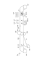
- FIGS. 1 and 2 are diagrams showing a defect inspection method and a manufacturing method for a laminated optical film according to the first embodiment of the present invention.
- 3 and 5 are views showing one main surface of the laminated optical film in different steps of the defect inspection method according to the first embodiment of the present invention, and
- FIGS. 4 and 6 are FIGS. 3 and 5.
- It is sectional drawing of the laminated optical film shown in FIG. 1 to 6 show XY plane coordinates.
- the X direction indicates the width direction of the laminated optical film
- the Y direction indicates the longitudinal direction of the laminated optical film.
- the optical film 11 is unwound from the original fabric roll 101.
- the optical film 11 includes an optical film body having optical properties.
- Examples of the optical film 11 include a polarizing plate having polarization characteristics and a retardation plate having birefringence.
- the optical film 11 when the optical film 11 is a polarizing plate, the optical film 11 includes a polarizer (Polyvinyl Alcohol: PVA) as an optical film body, and TAC (Triacetyl Cellulose) films are bonded to both sides of the main surface of the polarizer. .
- PVA Polyvinyl Alcohol
- TAC Triacetyl Cellulose
- a light inspection device disposed on the one main surface 11a side of the optical film 11 by irradiating the optical film 11 with light by a light source (not shown) disposed on the other main surface 11b side of the optical film 11
- the light transmitted through the optical film 11 is received by 111, and a defect inspection of the optical film 11 is performed based on the received transmitted light (first inspection step, transmission inspection).
- the protective film 12 is unwound from the raw fabric roll 102, and the protective film 12 is laminated on the one main surface 11 a side of the optical film 11.
- a PET (Polyethylene Terephthalate) film or the like is used as the protective film 12.
- the optical film 11 and the protective film 12 are bonded together by the bonding roll 103 to generate a laminated optical film 10A.
- the defect information (defect information) detected in the first inspection process is used as a code to form the laminated optical film. It records on the surface edge part by the side of the protective film 12 of 10 A of films (recording process).
- the coordinate information of these defects 20 is used as a bar code 40 and the laminated optical film is used. It records with respect to each defect 20 in the X direction edge part of the surface at the side of the protective film 12 of 10 A of films. 4 and 1 schematically show only one defect 20 in FIG. 3 and the barcode 40 corresponding to the defect 20.
- One bar code 40 may be recorded for every predetermined section in the Y direction (for example, every 60 mm interval). In this case, information on all the defects existing in the predetermined section may be collectively recorded on one barcode 40.
- the laminated optical film 10 ⁇ / b> A is wound around the original fabric roll 104.
- the laminated optical film 10 ⁇ / b> A is unwound from the original fabric roll 104, and the separate film (release film) 14 is bonded to the adhesive material 15 from the original fabric roll 105. 13 is fed out, and the adhesive film 13 with a separate film is laminated on the optical film 11 side of the laminated optical film 10A.
- PET Polyethylene Terephthalate
- the laminated optical film 10 ⁇ / b> A and the adhesive material 13 with a separate film are bonded together by the bonding roll 106 to generate a laminated optical film 10 ⁇ / b> B.
- the laminated optical film 10B is irradiated with light by a light source (not shown) arranged on the other main surface 10b side (separate film-attached adhesive material 13 side) of the laminated optical film 10B, and one side of the laminated optical film 10B.
- the light transmitted through the laminated optical film 10B is received by the inspector 115 arranged on the main surface 10a side (protective film 12 side) of the laminated optical film 10B, and defect inspection of the laminated optical film 10B is performed based on the received transmitted light (first). 2 inspection process, transmission inspection).
- the inspection device 115 is a transmission inspection device.
- the defect information recorded on the barcode 40 in the recording process is read by the code reader 117, and the defect 20 corresponding to the read defect information is not detected. That is, in the second inspection process, the defect 21 that is not detected in the first inspection process and is detected for the first time in the second inspection process is detected (see FIGS. 5 and 6). Specifically, in the second inspection step, a defect at the same position as the defect coordinate read from the barcode 40 is determined as the same defect and is not detected.
- FIG. 6 schematically shows one defect 20 in FIG. 5 and two linear marks 31 corresponding to the defect 20, and also corresponds to one defect 21 in FIG. 5 and the defect 21.
- Two linear marks 31 are schematically shown.
- FIG. 2 schematically shows only one defect 20 or 21 in FIG. 5 and two linear marks 31 corresponding to the defect 20 or 21.
- the laminated optical film 10 ⁇ / b> B is wound around the original fabric roll 107.
- FIGS. 7 and 9 are views showing one main surface of the laminated optical film in different steps of the conventional defect inspection method
- FIGS. 8 and 10 are laminated optical films shown in FIGS. FIG.
- the conventional defect inspection method includes a first marking step and a second marking step instead of the recording step and the marking step in the present embodiment, and does not detect the defect detected in the first inspection step in the second inspection step. This is different from the defect inspection method according to the present embodiment in that it does not have the function.
- the first marking step for example, as shown in FIG. 7 and FIG. 8, when three defects 20 are detected that are caused by mixing of foreign matter inside the laminated optical film 10 ⁇ / b> A, X for each of these defects 20 is detected. Marking on the surface of the laminated optical film 10A on the protective film 12 side so as to sandwich the defect 20, in other words, by enclosing the defect 20 by marking the linear mark 30 in the Y direction on each side of the direction. I do.
- the second marking step for example, as shown in FIGS. 8 and 10, when two defects 21 caused by foreign matters mixed in the laminated optical film 10 ⁇ / b> B are detected, X for each of these defects 21 is detected.
- the defect 20 is detected again in the first inspection step, and the mark 30 formed in the first marking step is regarded as a defect. To detect.
- the second marking process corresponding to the defect 20 detected in the first inspection process and the mark 30 formed in the first marking process, these defects 20 and the mark 30 are sandwiched.
- a mark 31 is formed so as to surround the defect 20 and the mark 30.
- the defect inspection when the defect inspection is performed twice or more, defects detected before the previous time are detected in the second and subsequent inspections, and the defect rate can be accurately obtained. There is a problem that you can not. Further, in the second and subsequent inspections, the mark marked before the previous time is detected as a defect, and correspondingly, the mark is further marked in the vicinity of the defect. As a result, the final mark size is increased and the yield of the optical film is increased. There is a problem that decreases.
- the defect inspection method for the laminated optical film of the first embodiment since the defect corresponding to the defect information recorded in the recording process is not detected in the second inspection process, the defect inspection is performed twice or more. In addition, it is possible to prevent the defect 20 detected before the previous time from being duplicated, and as a result, the defect rate can be accurately obtained. Moreover, according to the defect inspection method for the laminated optical film of the first embodiment, the defect information detected in the first inspection step is recorded as the barcode 40 in the recording step, so that the second inspection step is performed. Since marking is not performed on the optical film corresponding to the defect 20 detected in the first inspection step, it is possible to prevent detection of a mark corresponding to the defect detected before the previous time. Therefore, it is possible to prevent a decrease in the yield of the optical film due to an increase in the final mark size. [Modification of First Embodiment]
- the method of performing the same kind of defect inspection in multiple times before and after the process of bonding the protective film 12 and the adhesive material 13 with a separate film to the optical film 11 was illustrated.
- the idea of the present invention is a mode in which different types of defect inspection are performed in combination, for example, in the first embodiment, a transmission inspection is performed as a first inspection step, and a second inspection step is performed.
- the present invention can also be applied to a form for performing a reflection inspection.
- different inspections may be performed in combination on the same laminated optical film.
- the transmission inspection is suitable for detecting black foreign matters mixed inside the optical film, but it is difficult to detect small bubbles mixed on the optical film surface.
- the reflection inspection is suitable for detecting small bubbles mixed on the optical film surface, but it is difficult to detect black foreign matters mixed inside the optical film.
- FIG. 11 and FIG. 12 are views showing a defect inspection method and a manufacturing method of a laminated optical film according to the second embodiment of the present invention.
- 13 and 15 are views showing one main surface of the laminated optical film in different steps of the defect inspection method for the laminated optical film according to the second embodiment of the present invention.
- FIG. 16 is a cross-sectional view of the laminated optical film shown in FIGS. 13 and 15.
- the laminated optical film 10 ⁇ / b> B is fed out from the original fabric roll 101. And by the light source (not shown) arrange
- the defect information detected in the first inspection step is used as a code to code the laminated optical film 10A. It records on the surface edge part by the side of the protective film 12 (recording process).
- the coordinate information of these defects 20 is used as a barcode 40, and the laminated optics It records with respect to each defect 20 in the X direction edge part of the surface at the side of the protective film 12 of 10 A of films. 14 and 11 schematically show only one defect 20 in FIG. 13 and the barcode 40 corresponding to the defect 20.
- the laminated optical film 10 ⁇ / b> B is wound around the original fabric roll 104.
- the laminated optical film 10 ⁇ / b> B is fed out from the original fabric roll 104.
- light was irradiated to the laminated optical film 10B by a light source (not shown) arranged on the one main surface 10a side of the laminated optical film 10B, and arranged on the one main surface 10a side of the laminated optical film 10B.
- the inspection device 115 receives the light reflected by the one main surface 10a of the laminated optical film 10B, and performs a defect inspection of the laminated optical film 10B based on the received reflected light (second inspection step, reflection inspection).
- the inspection device 115 is a reflection inspection device.
- the defect information recorded on the barcode 40 in the recording process is read by the code reader 117, and the defect 20 corresponding to the read defect information is not detected. That is, in the second inspection process, the defect 25 which is not detected in the first inspection process and is detected for the first time in the second inspection process is detected (see FIGS. 15 and 16). Specifically, in the second inspection step, a defect at the same position as the defect coordinate read from the barcode 40 is determined as the same defect and is not detected.
- FIG. 16 schematically shows one defect 20 in FIG. 15 and two linear marks 31 corresponding to the defect 20, and also corresponds to one defect 25 in FIG. 15 and the defect 25.
- Two linear marks 31 are schematically shown.
- FIG. 12 schematically shows only one defect 20 or 25 in FIG. 15 and two linear marks 31 corresponding to the defect 20 or 25.
- the laminated optical film 10 ⁇ / b> B is wound around the original fabric roll 107.
- the defect inspection method and manufacturing method of the laminated optical film of the second embodiment can also provide the same advantages as the defect inspection method and manufacturing method of the laminated optical film of the first embodiment.
- the present invention is not limited to the above-described embodiment, and various modifications can be made.
- the form in which the defect inspection is performed twice is illustrated, but the idea of the present invention can be applied to the form in which the defect inspection is performed three times or more.
- the transmission inspection and the reflection inspection are exemplified as the types of defect inspection, but the types of defect inspection are not limited thereto.
- the idea of the present invention can also be applied to a defect inspection method including a crossed Nicol inspection.
- the coordinate information of the detected defect 20 is recorded on the laminated optical film 10A as the barcode 40.
- the detected coordinate information of the defect 20 is recorded in a memory such as a computer. Also good.
- the coordinate information of the defect recorded on the barcode 40 is read by the code reader 117 in the second inspection step.
- the coordinate information recorded in the memory of a computer or the like is read. You may read.
- 10A, 10B ... laminated optical film, 11 ... optical film, 12 ... protective film, 13 ... adhesive material with separate film, 14 ... separate film, 15 ... adhesive material, 20, 21, 25 ... defect, 30, 31 ... mark, 40 ... Bar code (code), 101, 102, 104, 105, 107 ... Raw roll, 103, 106 ... Laminating roll, 111 ... Transmission inspection device, 113, 119 ... Inkjet printer, 115 ... Inspection device (transmission) (Inspector or reflection inspector) 117: Code reader.
Landscapes
- General Health & Medical Sciences (AREA)
- General Physics & Mathematics (AREA)
- Physics & Mathematics (AREA)
- Health & Medical Sciences (AREA)
- Life Sciences & Earth Sciences (AREA)
- Chemical & Material Sciences (AREA)
- Analytical Chemistry (AREA)
- Biochemistry (AREA)
- Pathology (AREA)
- Immunology (AREA)
- Engineering & Computer Science (AREA)
- Textile Engineering (AREA)
- Computer Vision & Pattern Recognition (AREA)
- Signal Processing (AREA)
- Investigating Materials By The Use Of Optical Means Adapted For Particular Applications (AREA)
- Manufacturing Optical Record Carriers (AREA)
- Testing Of Optical Devices Or Fibers (AREA)
Abstract
積層光学フィルムの欠陥検査方法は、光学フィルム11の欠陥検査を行う第1検査工程と、光学フィルム11に保護フィルム12及び粘着材13を貼り合せて積層光学フィルム10A,10Bを生成する工程と、第1検査工程において検出された欠陥20の情報をコード40として積層光学フィルム10Aに記録する記録工程と、積層光学フィルム10Bの欠陥検査を行う第2検査工程と、第1検査工程において検出された欠陥20、及び、第2検査工程において検出された欠陥21に対応して積層光学フィルム10Bにマーキングを行うマーキング工程とを含み、第2検査工程では、記録工程において記録した欠陥情報を読み取り、当該欠陥情報に対応する欠陥20を重複検出しない。
Description
本発明は、積層光学フィルムの欠陥検査方法及び光学フィルムの欠陥検査方法に関し、積層光学フィルムの製造方法にも関する。
光学特性を有する光学フィルムとして、偏光特性を有する偏光板、複屈折性を有する位相差板などが知られている。例えば、偏光板として、光学フィルム本体としての偏光子(Polyvinyl Alcohol:PVA)の主面両側にTAC(Triacetyl Cellulose)フィルムが貼り合わされたものが知られている。位相差板として、位相差板が光学フィルム本体単独からなるものが知られている。この種の光学フィルムには、保護フィルムが貼合されたり、セパレートフィルムが付いた状態の粘着材が貼合されて積層光学フィルムとされることもある。
この種の光学フィルム及び積層光学フィルムでは、例えば上記貼合の際に、内部又は表面に異物や気泡が混入すると、光学的な欠陥が生じることがある。特許文献1~2には、この種の光学フィルム及び積層光学フィルムの欠陥を検査する方法が開示されている。
この種の欠陥検査方法によって欠陥が検出されると、欠陥に対応して、例えば欠陥を囲うように、光学フィルム及び積層光学フィルムの表面上にマーキングが行われ、マーキングが行われた領域は、製品としての利用から除かれる。
このような欠陥検査方法では、欠陥の数を過不足なく正確に数えることが求められる。また、マーキングされるマークは、欠陥の大きさに対応した大きさであることが求められる。
ところで、この種の光学フィルム及び積層光学フィルムの欠陥検査では、2回以上の欠陥検査を行うことがある。例えば、光学フィルム及び積層光学フィルムの各層を貼合するごとに欠陥検査を行ったり、異なる欠陥を検出するために異なる検査方法を行ったりすることがある。
しかしながら、2回以上の欠陥検査を行う場合、2回目以降の検査において、前回以前に検出された欠陥を重複検出してしまい、欠陥率を精度よく求められないという問題がある。2回目以降の検査において、前回以前にマーキングされたマークを欠陥として検出して、それに対応して(例えば欠陥を囲うように)マーキングしてしまい、その結果、最終マークサイズが大きくなってしまうという問題がある。
そこで、本発明は、2回以上の欠陥検査を行う際に、前回以前に検出された欠陥を重複検出すること、及び、前回以前に検出された欠陥に対応するマークを検出することを防止することが可能な積層光学フィルムの欠陥検査方法及び光学フィルムの欠陥検査方法を提供することを目的とする。また、本発明は、積層光学フィルムの製造方法を提供することをも目的とする。
本発明の積層光学フィルムの欠陥検査方法は、光学フィルムに保護フィルム及び粘着材の少なくとも一方を貼り合せて積層光学フィルムを得ながら、積層光学フィルム中の欠陥を検査する方法であって、光学フィルムの欠陥検査を行う第1検査工程と、光学フィルムに保護フィルム及び粘着材の少なくとも一方を貼り合せて積層光学フィルムを生成する工程と、第1検査工程において検出された欠陥情報を記録する記録工程と、積層光学フィルムの欠陥検査を行う第2検査工程と、第1検査工程において検出された欠陥、及び、第2検査工程において検出された欠陥に対応して積層光学フィルムにマーキングを行うマーキング工程とを含み、第2検査工程では、記録工程において記録した欠陥情報を読み取り、当該欠陥情報に対応する欠陥を検出しない。
この積層光学フィルムの欠陥検査方法によれば、第2検査工程では、記録工程において記録した欠陥情報に対応する欠陥を検出しない。よって、2回以上の欠陥検査を行う際に、前回以前に検出された欠陥を重複検出することを防止できる。また、この積層光学フィルムの欠陥検査方法によれば、記録工程において、第1検査工程で検出された欠陥情報を記録することにより、第2検査工程の前に第1検査工程で検出された欠陥に対応して光学フィルムにマーキングを行わないので、前回以前に検出された欠陥に対応するマークを検出することを防止できる。
上記した第1検査工程における欠陥検査方法と上記した第2検査工程における欠陥検査方法とは、同一であってもよいし、異なっていてもよい。
本発明の光学フィルムの欠陥検査方法は、光学フィルムの欠陥を検査する方法であって、光学フィルムの欠陥検査を行う第1検査工程と、第1検査工程において検出された欠陥情報を記録する記録工程と、光学フィルムに対して、第1検査工程における欠陥検査とは異なる欠陥検査を行う第2検査工程と、第1検査工程において検出された欠陥、及び、第2検査工程において検出された欠陥に対応して光学フィルムにマーキングを行うマーキング工程とを含み、第2検査工程では、記録工程において記録した欠陥情報を読み取り、当該欠陥情報に対応する欠陥を検出しない。
この発明における光学フィルムは、光学フィルム本体からなる単層光学フィルムのみならず、光学フィルム本体を含む光学フィルム、及び、その光学フィルムに保護フィルム及び粘着材の少なくとも一方を貼り合せた積層光学フィルムをも含む概念である。
この光学フィルムの欠陥検査方法でも、第2検査工程では、記録工程において記録した欠陥情報に対応する欠陥を検出しないので、2回以上の欠陥検査を行う際に、前回以前に検出された欠陥を重複検出することを防止できる。この光学フィルムの欠陥検査方法でも、記録工程において、第1検査工程で検出された欠陥情報を記録することにより、第2検査工程の前に第1検査工程で検出された欠陥に対応して光学フィルムにマーキングを行わないので、前回以前に検出された欠陥に対応するマークを検出することを防止できる。
本発明の積層光学フィルムの製造方法は、光学フィルムに保護フィルム及び粘着材の少なくとも一方を貼り合せて積層光学フィルムを製造する方法であって、上記した積層光学フィルムの欠陥検査方法を含む。この積層光学フィルムの製造方法によれば、上記した積層光学フィルムの欠陥検査方法と同様の利点が得られる。
本発明によれば、光学フィルム及び積層光学フィルムの欠陥検査を2回以上行う際に、前回以前に検出された欠陥を重複検出することを防止でき、その結果、欠陥率を精度よく求められる。また、本発明によれば、光学フィルム及び積層光学フィルムの欠陥検査を2回以上行う際に、前回以前に検出された欠陥に対応するマークを検出することを防止でき、その結果、最終マークサイズが大きくなってしまい、光学フィルムの収率が低下してしまうことを防止できる。
以下、図面を参照して本発明の好適な実施形態について詳細に説明する。なお、各図面において同一又は相当の部分に対しては同一の符号を附すこととする。
[第1の実施形態]
[第1の実施形態]
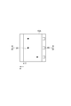
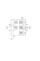
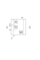
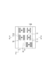
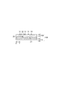
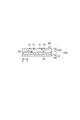
図1及び図2は、本発明の第1の実施形態に係る積層光学フィルムの欠陥検査方法及び製造方法を示す図である。図3及び図5は、本発明の第1の実施形態に係る欠陥検査方法の異なる工程における積層光学フィルムの一方の主面を示す図であり、図4及び図6は、図3及び図5に示す積層光学フィルムの断面図である。図1~図6には、XY平面座標が示されている。X方向は積層光学フィルムの幅方向を示し、Y方向は積層光学フィルムの長手方向を示す。
まず、図1に示すように、原反ロール101から光学フィルム11を繰り出す。光学フィルム11は、光学特性を有する光学フィルム本体を含む。光学フィルム11としては、偏光特性を有する偏光板、複屈折性を有する位相差板などが挙げられる。例えば、光学フィルム11が偏光板である場合、光学フィルム11は光学フィルム本体として偏光子(Polyvinyl Alcohol:PVA)を含み、この偏光子の主面両側にTAC(Triacetyl Cellulose)フィルムが貼り合わされている。一方、光学フィルム11が位相差板である場合、位相差板が光学フィルム本体に相当する。
次いで、光学フィルム11の他方の主面11b側に配置された光源(図示せず)によって、光学フィルム11に光を照射し、光学フィルム11の一方の主面11a側に配置された透過検査器111によって、光学フィルム11を透過した光を受光し、受光した透過光に基づいて光学フィルム11の欠陥検査を行う(第1検査工程、透過検査)。
次いで、原反ロール102から保護フィルム12を繰り出し、保護フィルム12を光学フィルム11の一方の主面11a側に積層する。保護フィルム12としてはPET(Polyethylene Terephthalate)フィルムなどが用いられる。次いで、貼合ロール103によって光学フィルム11と保護フィルム12とを貼り合わせ、積層光学フィルム10Aを生成する。
次いで、積層光学フィルム10Aの保護フィルム12側に配置されたインクジェット印刷器113を用いて(液滴法によって)、第1検査工程で検出された欠陥の情報(欠陥情報)をコードとして、積層光学フィルム10Aの保護フィルム12側の表面端部に記録する(記録工程)。
例えば、図3及び図4に示すように、積層光学フィルム10A内部に異物が混入することによって生じる3つの欠陥20が検出された場合、これらの欠陥20の座標情報をバーコード40として、積層光学フィルム10Aの保護フィルム12側の表面のX方向端部に、各欠陥20に対して記録する。図4及び図1では、図3における1つの欠陥20、及び、この欠陥20に対応するバーコード40のみを概略的に示す。
Y方向の所定区間ごとに(例えば、60mm間隔ごとに)、1つのバーコード40を記録してもよい。この場合、所定区間に存在する欠陥全ての情報を纏めて1つのバーコード40に記録すればよい。
次いで、原反ロール104に積層光学フィルム10Aを巻き取る。
次いで、図2に示すように、原反ロール104から積層光学フィルム10Aを繰り出し、また、原反ロール105から、セパレートフィルム(離型フィルム)14が粘着材15に貼り合わされたセパレートフィルム付き粘着材13を繰り出し、積層光学フィルム10Aの光学フィルム11側にセパレートフィルム付き粘着材13を積層する。セパレートフィルムの材料としてはPET(Polyethylene Terephthalate)などが用いられる。次いで、貼合ロール106によって積層光学フィルム10Aとセパレートフィルム付き粘着材13とを貼り合わせ、積層光学フィルム10Bを生成する。
次いで、積層光学フィルム10Bの他方の主面10b側(セパレートフィルム付き粘着材13側)に配置された光源(図示せず)によって、積層光学フィルム10Bに光を照射し、積層光学フィルム10Bの一方の主面10a側(保護フィルム12側)に配置された検査器115によって、積層光学フィルム10Bを透過した光を受光し、受光した透過光に基づいて積層光学フィルム10Bの欠陥検査を行う(第2検査工程、透過検査)。第1の実施形態において、検査器115は、透過検査器である。
第2検査工程では、コード読取器117によって、記録工程でバーコード40に記録した欠陥情報を読み取り、読み取った欠陥情報に対応する欠陥20を検出しない。すなわち、第2検査工程では、第1検査工程では検出されておらず、第2検査工程で初めて検出された欠陥21を検出する(図5及び図6を参照)。具体的には、第2検査工程では、バーコード40から読み取った欠陥座標と同じ位置の欠陥を同一欠陥と判別して検出しない。
次いで、積層光学フィルム10Bの一方の主面10a側に配置されたインクジェット印刷器119を用いて(液滴法によって)、第1検査工程で検出された欠陥(すなわち、バーコード40から読み取った欠陥)、及び、第2検査工程で検出された欠陥に対応して、積層光学フィルム10Bの一方の主面10a側の表面にマーキングを行う(マーキング工程)。
例えば、図3及び図4に示すように、第1検査工程において、積層光学フィルム10A内部に異物が混入することによって生じる3つの欠陥20が検出され、図5及び図6に示すように、第2検査工程において、積層光学フィルム10B内部に異物が混入することによって生じる2つの欠陥21が検出された場合、これらの欠陥20,21それぞれに対してX方向の両側それぞれに、線状のマーク31をY方向にマーキングすることによって、欠陥20,21を挟み込むように、換言すれば欠陥20,21を囲うように、積層光学フィルム10Bの一方の主面10a側の表面にマーキングを行う。
図6では、図5における1つの欠陥20、及び、この欠陥20に対応する2つの線状のマーク31を概略的に示すと共に、図5における1つの欠陥21、及び、この欠陥21に対応する2つの線状のマーク31を概略的に示す。図2では、図5における1つの欠陥20又は21、及び、この欠陥20又は21に対応する2つの線状のマーク31のみを概略的に示す。
次いで、積層光学フィルム10Bを原反ロール107に巻き取る。
ここで、図7及び図9は、従来の欠陥検査方法の異なる工程における積層光学フィルムの一方の主面を示す図であり、図8及び図10は、図7及び図9に示す積層光学フィルムの断面図である。
従来の欠陥検査方法では、本実施形態において記録工程及びマーキング工程に代えて、第1マーキング工程及び第2マーキング工程を備え、第2検査工程において、第1検査工程で検出された欠陥を検出しないという機能を備えていない点で、本実施形態の欠陥検査方法と相違する。
第1マーキング工程では、例えば、図7及び図8に示すように、積層光学フィルム10A内部に異物が混入することによって生じる3つの欠陥20が検出された場合、これらの欠陥20それぞれに対してX方向の両側それぞれに、線状のマーク30をY方向にマーキングすることによって、欠陥20を挟み込むように、換言すれば欠陥20を囲うように、積層光学フィルム10Aの保護フィルム12側の表面にマーキングを行う。
第2マーキング工程では、例えば、図8及び図10に示すように、積層光学フィルム10B内部に異物が混入することによって生じる2つの欠陥21が検出された場合、これらの欠陥21それぞれに対してX方向の両側それぞれに、線状のマーク31をY方向にマーキングすることによって、欠陥21を挟み込むように、換言すれば欠陥21を囲うように、積層光学フィルム10Bの一方の主面10a側の表面にマーキングを行う。
この従来の欠陥検査方法では、図8及び図10に示すように、第2検査工程において、第1検査工程で欠陥20を再度検出すると共に、第1マーキング工程で形成されたマーク30を欠陥として検出する。その結果、第2マーキング工程において、第1検査工程で検出された欠陥20及び第1マーキング工程で形成されたマーク30に対応して、これらの欠陥20及びマーク30を挟み込むように、換言すれば欠陥20及びマーク30を囲うように、マーク31が形成される。
このように、従来の欠陥検査方法では、2回以上の欠陥検査を行う場合、2回目以降の検査において、前回以前に検出された欠陥を重複検出してしまい、欠陥率を精度よく求めることができないという問題がある。また、2回目以降の検査において、前回以前にマーキングされたマークを欠陥として検出して、それに対応して欠陥の近傍に更にマーキングし、その結果、最終マークサイズが大きくなり、光学フィルムの収率が低下するという問題がある。
しかしながら、第1の実施形態の積層光学フィルムの欠陥検査方法によれば、第2検査工程では、記録工程において記録した欠陥情報に対応する欠陥を検出しないので、2回以上の欠陥検査を行う際に、前回以前に検出された欠陥20を重複検出することを防止でき、その結果、欠陥率を精度よく求められる。また、第1の実施形態の積層光学フィルムの欠陥検査方法によれば、記録工程において、第1検査工程で検出された欠陥情報をバーコード40として記録することにより、第2検査工程の前に第1検査工程で検出された欠陥20に対応して光学フィルムにマーキングを行わないので、前回以前に検出された欠陥に対応するマークを検出することを防止できる。そのため、最終マークサイズが大きくなることによる光学フィルムの収率の低下を防止できる。
[第1の実施形態の変形例]
[第1の実施形態の変形例]
第1の実施形態では、光学フィルム11に保護フィルム12及びセパレートフィルム付き粘着材13を貼り合わせる工程の前と後とで同一の種類の欠陥検査(透過検査)を複数回行う方法を例示した。しかしながら、本発明の思想は、以下に詳説するように、異なる種類の欠陥検査を組み合わせて行う形態、例えば、第1の実施形態において、第1検査工程として透過検査を行い、第2検査工程として反射検査を行う形態にも適用可能である。
[第2の実施形態]
[第2の実施形態]
第1の実施形態では、光学フィルム11に保護フィルム12及びセパレートフィルム付き粘着材13を貼り合わせる工程の前と後とで複数回の欠陥検査を行う方法を例示したが、本発明の思想は、同一の積層光学フィルムに対して複数回の欠陥検査を行う方法にも適用可能である。
例えば、同一の積層光学フィルムに対して、異なる検査(例えば、透過検査及び反射検査)を組み合わせて行う場合がある。例えば、透過検査は、光学フィルム内部に混入する黒色系の異物の検出に適しているが、光学フィルム表面に混入する小さい気泡の検出が困難である。一方、反射検査は、光学フィルム表面に混入する小さい気泡の検出に適しているが、光学フィルム内部に混入する黒色系の異物の検出が困難である。
以下に、同一の積層光学フィルムに対して異なる検査を組み合わせて行う欠陥検査方法を例示する。この第2の実施形態では、積層光学フィルムの欠陥検査方法を例示する。しかしながら、本発明の思想は、単層光学フィルムに対して異なる検査を組み合わせて行う欠陥検査方法にも適用可能である。
図11及び図12は、本発明の第2の実施形態に係る積層光学フィルムの欠陥検査方法及び製造方法を示す図である。図13及び図15は、本発明の第2の実施形態に係る積層光学フィルムの欠陥検査方法の異なる工程における積層光学フィルムの一方の主面を示す図であり、図14及び図16は、図13及び図15に示す積層光学フィルムの断面図である。
まず、図11に示すように、原反ロール101から積層光学フィルム10Bを繰り出す。そして、積層光学フィルム10Bの他方の主面10b側に配置された光源(図示せず)によって、積層光学フィルム10Bに光を照射し、積層光学フィルム10Bの一方の主面10a側に配置された透過検査器111によって、積層光学フィルム10Bを透過した光を受光し、受光した透過光に基づいて積層光学フィルム10Bの欠陥検査を行う(第1検査工程、透過検査)。
次いで、積層光学フィルム10Bの一方の主面10a側に配置されたインクジェット印刷器113を用いて(液滴法によって)、第1検査工程で検出された欠陥情報をコードとして、積層光学フィルム10Aの保護フィルム12側の表面端部に記録する(記録工程)。
例えば、図13及び図14に示すように、積層光学フィルム10B内部に異物が混入することによって生じる3つの欠陥20が検出された場合、これらの欠陥20の座標情報をバーコード40として、積層光学フィルム10Aの保護フィルム12側の表面のX方向端部に、各欠陥20に対して記録する。図14及び図11では、図13における1つの欠陥20、及び、この欠陥20に対応するバーコード40のみを概略的に示す。
次いで、原反ロール104に積層光学フィルム10Bを巻き取る。
次いで、図12に示すように、原反ロール104から積層光学フィルム10Bを繰り出す。次いで、積層光学フィルム10Bの一方の主面10a側に配置された光源(図示せず)によって、積層光学フィルム10Bに光を照射し、積層光学フィルム10Bの一方の主面10a側に配置された検査器115によって、積層光学フィルム10Bの一方の主面10aで反射した光を受光し、受光した反射光に基づいて積層光学フィルム10Bの欠陥検査を行う(第2検査工程、反射検査)。第2の実施形態において、検査器115は反射検査器である。
第2検査工程では、コード読取器117によって、記録工程でバーコード40に記録した欠陥情報を読み取り、読み取った欠陥情報に対応する欠陥20を検出しない。すなわち、第2検査工程では、第1検査工程では検出されておらず、第2検査工程で初めて検出された欠陥25を検出する(図15及び図16を参照)。具体的には、第2検査工程では、バーコード40から読み取った欠陥座標と同じ位置の欠陥を同一欠陥と判別して検出しない。
次いで、積層光学フィルム10Bの一方の主面10a側に配置されたインクジェット印刷器119を用いて(液滴法によって)、第1検査工程で検出された欠陥(すなわち、バーコード40から読み取った欠陥)、及び、第2検査工程で検出された欠陥に対応して、積層光学フィルム10Bの一方の主面10a側の表面にマーキングを行う(マーキング工程)。
例えば、図13及び図14に示すように、第1検査工程において、積層光学フィルム10B内部に異物が混入することによって生じる3つの欠陥20が検出され、図15及び図16に示すように、第2検査工程において、積層光学フィルム10B表面に気泡が混入することによって生じる2つの欠陥25が検出された場合、これらの欠陥20,25それぞれに対してX方向の両側それぞれに、線状のマーク31をY方向にマーキングすることによって、欠陥20,25を挟み込むように、換言すれば欠陥20,25を囲うように、積層光学フィルム10Bの一方の主面10a側の表面にマーキングを行う。
図16では、図15における1つの欠陥20、及び、この欠陥20に対応する2つの線状のマーク31を概略的に示すと共に、図15における1つの欠陥25、及び、この欠陥25に対応する2つの線状のマーク31を概略的に示す。図12では、図15における1つの欠陥20又は25、及び、この欠陥20又は25に対応する2つの線状のマーク31のみを概略的に示す。
次いで、積層光学フィルム10Bを原反ロール107に巻き取る。
この第2の実施形態の積層光学フィルムの欠陥検査方法及び製造方法でも、第1の実施形態の積層光学フィルムの欠陥検査方法及び製造方法と同様の利点を得ることができる。
本発明は上記した本実施形態に限定されることなく種々の変形が可能である。例えば、本実施形態では、欠陥検査を2回行う形態を例示したが、本発明の思想は、欠陥検査を3回以上行う形態にも適用可能である。
本実施形態では、欠陥検査の種類として透過検査及び反射検査を例示したが、欠陥検査の種類はこれに限定されない。本発明の思想は、クロスニコル検査などを含む欠陥検査方法にも適用可能である。
本実施形態では、記録工程において、検出した欠陥20の座標情報をバーコード40として積層光学フィルム10Aに記録したが、記録工程において、検出した欠陥20の座標情報をコンピュータ等のメモリーに記録してもよい。また、本実施形態では、第2検査工程において、コード読取器117によってバーコード40に記録した欠陥の座標情報を読み取ったが、第2検査工程において、コンピュータ等のメモリーに記録された座標情報を読み取ってもよい。
10A,10B…積層光学フィルム、11…光学フィルム、12…保護フィルム、13…セパレートフィルム付き粘着材、14…セパレートフィルム、15…粘着材、20,21,25…欠陥、30,31…マーク、40…バーコード(コード)、101,102,104,105,107…原反ロール、103、106…貼合ロール、111…透過検査器、113,119…インクジェット印刷器、115…検査器(透過検査器又は反射検査器)、117…コード読取器。
Claims (5)
- 光学フィルムに保護フィルム及び粘着材の少なくとも一方を貼り合せて積層光学フィルムを得ながら、前記積層光学フィルム中の欠陥を検査する方法であって、
前記光学フィルムの欠陥検査を行う第1検査工程と、
前記光学フィルムに前記保護フィルム及び前記粘着材の少なくとも一方を貼り合せて前記積層光学フィルムを生成する工程と、
前記第1検査工程において検出された欠陥情報を記録する記録工程と、
前記積層光学フィルムの欠陥検査を行う第2検査工程と、
前記第1検査工程において検出された欠陥、及び、前記第2検査工程において検出された欠陥に対応して前記積層光学フィルムにマーキングを行うマーキング工程と、
を含み、
前記第2検査工程では、前記記録工程において記録した前記欠陥情報を読み取り、当該欠陥情報に対応する欠陥を検出しない、
積層光学フィルムの欠陥検査方法。 - 前記第1検査工程における欠陥検査方法と前記第2検査工程における欠陥検査方法とは同一である、請求項1に記載の積層光学フィルムの欠陥検査方法。
- 前記第1検査工程における欠陥検査方法と前記第2検査工程における欠陥検査方法とは異なる、請求項1に記載の積層光学フィルムの欠陥検査方法。
- 光学フィルムの欠陥を検査する方法であって、
前記光学フィルムの欠陥検査を行う第1検査工程と、
前記第1検査工程において検出された欠陥情報を記録する記録工程と、
前記光学フィルムに対して、前記第1検査工程における欠陥検査とは異なる欠陥検査を行う第2検査工程と、
前記第1検査工程において検出された欠陥、及び、前記第2検査工程において検出された欠陥に対応して前記光学フィルムにマーキングを行うマーキング工程と、
を含み、
前記第2検査工程では、前記記録工程において記録した前記欠陥情報を読み取り、当該欠陥情報に対応する欠陥を検出しない、
光学フィルムの欠陥検査方法。 - 光学フィルムに保護フィルム及び粘着材の少なくとも一方を貼り合せて積層光学フィルムを製造する方法であって、
請求項1~3の何れか1項に記載の積層光学フィルムの欠陥検査方法を含む、
積層光学フィルムの製造方法。
Priority Applications (3)
| Application Number | Priority Date | Filing Date | Title |
|---|---|---|---|
| KR1020177022933A KR101890083B1 (ko) | 2015-03-20 | 2016-03-14 | 적층 광학 필름의 결함 검사 방법, 광학 필름의 결함 검사 방법 및 적층 광학 필름의 제조 방법 |
| CN202211437789.8A CN115728308A (zh) | 2015-03-20 | 2016-03-14 | 层叠光学膜、光学膜的缺陷检查方法及层叠光学膜的制法 |
| CN201680011973.2A CN107407641A (zh) | 2015-03-20 | 2016-03-14 | 层叠光学膜的缺陷检查方法、光学膜的缺陷检查方法以及层叠光学膜的制造方法 |
Applications Claiming Priority (2)
| Application Number | Priority Date | Filing Date | Title |
|---|---|---|---|
| JP2015-057729 | 2015-03-20 | ||
| JP2015057729A JP6641093B2 (ja) | 2015-03-20 | 2015-03-20 | 光学フィルム及び積層光学フィルムの欠陥検査方法 |
Publications (1)
| Publication Number | Publication Date |
|---|---|
| WO2016152628A1 true WO2016152628A1 (ja) | 2016-09-29 |
Family
ID=56979227
Family Applications (1)
| Application Number | Title | Priority Date | Filing Date |
|---|---|---|---|
| PCT/JP2016/058024 Ceased WO2016152628A1 (ja) | 2015-03-20 | 2016-03-14 | 積層光学フィルムの欠陥検査方法、光学フィルムの欠陥検査方法及び積層光学フィルムの製造方法 |
Country Status (5)
| Country | Link |
|---|---|
| JP (1) | JP6641093B2 (ja) |
| KR (1) | KR101890083B1 (ja) |
| CN (2) | CN107407641A (ja) |
| TW (1) | TWI718132B (ja) |
| WO (1) | WO2016152628A1 (ja) |
Cited By (1)
| Publication number | Priority date | Publication date | Assignee | Title |
|---|---|---|---|---|
| CN107703152A (zh) * | 2017-10-27 | 2018-02-16 | 深圳精创视觉科技有限公司 | 光学膜缺点自动标示装置 |
Families Citing this family (6)
| Publication number | Priority date | Publication date | Assignee | Title |
|---|---|---|---|---|
| JP6749894B2 (ja) * | 2015-04-09 | 2020-09-02 | 住友化学株式会社 | 積層光学フィルムの欠陥検査方法、光学フィルムの欠陥検査方法及び積層光学フィルムの製造方法 |
| KR102475056B1 (ko) * | 2017-03-03 | 2022-12-06 | 스미또모 가가꾸 가부시키가이샤 | 결함 마킹 방법 및 결함 마킹 장치, 원반의 제조 방법 및 원반, 그리고 시트의 제조 방법 및 시트 |
| KR102603009B1 (ko) * | 2017-09-05 | 2023-11-15 | 스미또모 가가꾸 가부시키가이샤 | 결함 기록 시스템 및 필름 제조 시스템, 그리고 필름의 제조 방법 |
| WO2021117273A1 (ja) * | 2019-12-10 | 2021-06-17 | 日東電工株式会社 | 長尺光学積層体の検査方法及び検査システム |
| CN111452514B (zh) * | 2020-04-26 | 2021-01-12 | 杭州利珀科技有限公司 | 偏光膜整线打标系统及方法 |
| KR20230058613A (ko) * | 2020-08-31 | 2023-05-03 | 닛토덴코 가부시키가이샤 | 광학 적층체의 검사 방법 |
Citations (4)
| Publication number | Priority date | Publication date | Assignee | Title |
|---|---|---|---|---|
| JP2008116438A (ja) * | 2006-10-11 | 2008-05-22 | Nitto Denko Corp | 検査データ処理装置及び検査データ処理方法 |
| JP2008164336A (ja) * | 2006-12-27 | 2008-07-17 | Olympus Corp | 欠陥検査システムおよび方法 |
| JP2009069142A (ja) * | 2007-08-23 | 2009-04-02 | Nitto Denko Corp | 積層フィルムの欠陥検査方法およびその装置 |
| JP2009244064A (ja) * | 2008-03-31 | 2009-10-22 | Sumitomo Chemical Co Ltd | 偏光フィルムの検査方法 |
Family Cites Families (8)
| Publication number | Priority date | Publication date | Assignee | Title |
|---|---|---|---|---|
| TWI265325B (en) * | 2003-01-23 | 2006-11-01 | Nippon Oil Corp | Manufacturing method of optically laminated body, elliptic polarization plate formed by the laminated body, circular polarization plate and liquid crystal display apparatus |
| TWI366706B (en) * | 2006-07-03 | 2012-06-21 | Olympus Corp | Semiconductor substrate defects detection device and method of detection of defects |
| JP4776739B2 (ja) | 2009-04-10 | 2011-09-21 | 日東電工株式会社 | 光学フィルムロール原反を用いた画像表示装置の製造方法 |
| JP2012173044A (ja) * | 2011-02-18 | 2012-09-10 | Jfe Steel Corp | 鋼板の表面疵検査装置 |
| KR101311497B1 (ko) | 2011-10-20 | 2013-10-14 | 주식회사 엘지화학 | 광학 필름의 결함 검사 장치 |
| JP2013134136A (ja) * | 2011-12-26 | 2013-07-08 | Jfe Steel Corp | 表面欠陥検査システム |
| JP6177017B2 (ja) * | 2013-06-12 | 2017-08-09 | 住友化学株式会社 | 欠陥検査システム |
| JP2015049350A (ja) | 2013-08-30 | 2015-03-16 | 住友化学株式会社 | 光学部材貼合体の製造方法 |
-
2015
- 2015-03-20 JP JP2015057729A patent/JP6641093B2/ja active Active
-
2016
- 2016-03-14 KR KR1020177022933A patent/KR101890083B1/ko active Active
- 2016-03-14 CN CN201680011973.2A patent/CN107407641A/zh active Pending
- 2016-03-14 WO PCT/JP2016/058024 patent/WO2016152628A1/ja not_active Ceased
- 2016-03-14 CN CN202211437789.8A patent/CN115728308A/zh active Pending
- 2016-03-18 TW TW105108546A patent/TWI718132B/zh active
Patent Citations (4)
| Publication number | Priority date | Publication date | Assignee | Title |
|---|---|---|---|---|
| JP2008116438A (ja) * | 2006-10-11 | 2008-05-22 | Nitto Denko Corp | 検査データ処理装置及び検査データ処理方法 |
| JP2008164336A (ja) * | 2006-12-27 | 2008-07-17 | Olympus Corp | 欠陥検査システムおよび方法 |
| JP2009069142A (ja) * | 2007-08-23 | 2009-04-02 | Nitto Denko Corp | 積層フィルムの欠陥検査方法およびその装置 |
| JP2009244064A (ja) * | 2008-03-31 | 2009-10-22 | Sumitomo Chemical Co Ltd | 偏光フィルムの検査方法 |
Cited By (1)
| Publication number | Priority date | Publication date | Assignee | Title |
|---|---|---|---|---|
| CN107703152A (zh) * | 2017-10-27 | 2018-02-16 | 深圳精创视觉科技有限公司 | 光学膜缺点自动标示装置 |
Also Published As
| Publication number | Publication date |
|---|---|
| JP6641093B2 (ja) | 2020-02-05 |
| KR20170117429A (ko) | 2017-10-23 |
| TWI718132B (zh) | 2021-02-11 |
| KR101890083B1 (ko) | 2018-08-20 |
| CN107407641A (zh) | 2017-11-28 |
| JP2016176836A (ja) | 2016-10-06 |
| CN115728308A (zh) | 2023-03-03 |
| TW201719152A (zh) | 2017-06-01 |
Similar Documents
| Publication | Publication Date | Title |
|---|---|---|
| WO2016152628A1 (ja) | 積層光学フィルムの欠陥検査方法、光学フィルムの欠陥検査方法及び積層光学フィルムの製造方法 | |
| JP6749894B2 (ja) | 積層光学フィルムの欠陥検査方法、光学フィルムの欠陥検査方法及び積層光学フィルムの製造方法 | |
| JP6177017B2 (ja) | 欠陥検査システム | |
| TWI766952B (zh) | 缺陷標記方法及缺陷標記裝置、原材的製造方法及原材,以及片的製造方法及片 | |
| CN101981438A (zh) | 偏光薄膜的检查方法 | |
| JP2009244064A5 (ja) | ||
| JP2019053057A (ja) | 欠陥検査装置、欠陥検査方法、円偏光板又は楕円偏光板の製造方法及び位相差板の製造方法 | |
| WO2015182541A1 (ja) | 積層偏光フィルムの欠陥検査方法、製造方法および製造装置 | |
| JP7086642B2 (ja) | 欠陥検査システム、フィルム製造装置、フィルム製造方法、印字装置及び印字方法 | |
| JP6437329B2 (ja) | 光学フィルムの欠陥検査方法 | |
| JP2019215371A (ja) | 光学フィルム及び積層光学フィルムの欠陥検査方法 | |
| CN114846321A (zh) | 功能膜检查方法、检查系统以及料卷 | |
| JP7288989B1 (ja) | 長尺光学フィルムの検査方法 | |
| JP7195042B2 (ja) | 欠陥情報読取方法、欠陥情報読取システム及びフィルム製造装置 | |
| TW202129264A (zh) | 長條光學積層體之檢查方法及檢查系統 | |
| CN114654096A (zh) | 带有标记的光学层叠体、以及带有标记的光学层叠体的制造方法 |
Legal Events
| Date | Code | Title | Description |
|---|---|---|---|
| 121 | Ep: the epo has been informed by wipo that ep was designated in this application |
Ref document number: 16768531 Country of ref document: EP Kind code of ref document: A1 |
|
| ENP | Entry into the national phase |
Ref document number: 20177022933 Country of ref document: KR Kind code of ref document: A |
|
| NENP | Non-entry into the national phase |
Ref country code: DE |
|
| 122 | Ep: pct application non-entry in european phase |
Ref document number: 16768531 Country of ref document: EP Kind code of ref document: A1 |