WO2016147308A1 - レーザシステム及びレーザアニール装置 - Google Patents
レーザシステム及びレーザアニール装置 Download PDFInfo
- Publication number
- WO2016147308A1 WO2016147308A1 PCT/JP2015/057779 JP2015057779W WO2016147308A1 WO 2016147308 A1 WO2016147308 A1 WO 2016147308A1 JP 2015057779 W JP2015057779 W JP 2015057779W WO 2016147308 A1 WO2016147308 A1 WO 2016147308A1
- Authority
- WO
- WIPO (PCT)
- Prior art keywords
- laser
- pulse
- optical path
- laser beam
- unit
- Prior art date
- Legal status (The legal status is an assumption and is not a legal conclusion. Google has not performed a legal analysis and makes no representation as to the accuracy of the status listed.)
- Ceased
Links
Images

















Classifications
-
- H—ELECTRICITY
- H10—SEMICONDUCTOR DEVICES; ELECTRIC SOLID-STATE DEVICES NOT OTHERWISE PROVIDED FOR
- H10P—GENERIC PROCESSES OR APPARATUS FOR THE MANUFACTURE OR TREATMENT OF DEVICES COVERED BY CLASS H10
- H10P72/00—Handling or holding of wafers, substrates or devices during manufacture or treatment thereof
- H10P72/04—Apparatus for manufacture or treatment
- H10P72/0431—Apparatus for thermal treatment
- H10P72/0436—Apparatus for thermal treatment mainly by radiation
-
- H—ELECTRICITY
- H01—ELECTRIC ELEMENTS
- H01S—DEVICES USING THE PROCESS OF LIGHT AMPLIFICATION BY STIMULATED EMISSION OF RADIATION [LASER] TO AMPLIFY OR GENERATE LIGHT; DEVICES USING STIMULATED EMISSION OF ELECTROMAGNETIC RADIATION IN WAVE RANGES OTHER THAN OPTICAL
- H01S3/00—Lasers, i.e. devices using stimulated emission of electromagnetic radiation in the infrared, visible or ultraviolet wave range
- H01S3/005—Optical devices external to the laser cavity, specially adapted for lasers, e.g. for homogenisation of the beam or for manipulating laser pulses, e.g. pulse shaping
- H01S3/0057—Temporal shaping, e.g. pulse compression, frequency chirping
-
- H—ELECTRICITY
- H10—SEMICONDUCTOR DEVICES; ELECTRIC SOLID-STATE DEVICES NOT OTHERWISE PROVIDED FOR
- H10P—GENERIC PROCESSES OR APPARATUS FOR THE MANUFACTURE OR TREATMENT OF DEVICES COVERED BY CLASS H10
- H10P14/00—Formation of materials, e.g. in the shape of layers or pillars
- H10P14/20—Formation of materials, e.g. in the shape of layers or pillars of semiconductor materials
-
- H—ELECTRICITY
- H10—SEMICONDUCTOR DEVICES; ELECTRIC SOLID-STATE DEVICES NOT OTHERWISE PROVIDED FOR
- H10P—GENERIC PROCESSES OR APPARATUS FOR THE MANUFACTURE OR TREATMENT OF DEVICES COVERED BY CLASS H10
- H10P34/00—Irradiation with electromagnetic or particle radiation of wafers, substrates or parts of devices
- H10P34/40—Irradiation with electromagnetic or particle radiation of wafers, substrates or parts of devices with high-energy radiation
- H10P34/42—Irradiation with electromagnetic or particle radiation of wafers, substrates or parts of devices with high-energy radiation with electromagnetic radiation, e.g. laser annealing
-
- H—ELECTRICITY
- H10—SEMICONDUCTOR DEVICES; ELECTRIC SOLID-STATE DEVICES NOT OTHERWISE PROVIDED FOR
- H10P—GENERIC PROCESSES OR APPARATUS FOR THE MANUFACTURE OR TREATMENT OF DEVICES COVERED BY CLASS H10
- H10P72/00—Handling or holding of wafers, substrates or devices during manufacture or treatment thereof
- H10P72/06—Apparatus for monitoring, sorting, marking, testing or measuring
- H10P72/0612—Production flow monitoring, e.g. for increasing throughput
-
- H—ELECTRICITY
- H01—ELECTRIC ELEMENTS
- H01S—DEVICES USING THE PROCESS OF LIGHT AMPLIFICATION BY STIMULATED EMISSION OF RADIATION [LASER] TO AMPLIFY OR GENERATE LIGHT; DEVICES USING STIMULATED EMISSION OF ELECTROMAGNETIC RADIATION IN WAVE RANGES OTHER THAN OPTICAL
- H01S3/00—Lasers, i.e. devices using stimulated emission of electromagnetic radiation in the infrared, visible or ultraviolet wave range
- H01S3/02—Constructional details
- H01S3/03—Constructional details of gas laser discharge tubes
- H01S3/036—Means for obtaining or maintaining the desired gas pressure within the tube, e.g. by gettering, replenishing; Means for circulating the gas, e.g. for equalising the pressure within the tube
-
- H—ELECTRICITY
- H01—ELECTRIC ELEMENTS
- H01S—DEVICES USING THE PROCESS OF LIGHT AMPLIFICATION BY STIMULATED EMISSION OF RADIATION [LASER] TO AMPLIFY OR GENERATE LIGHT; DEVICES USING STIMULATED EMISSION OF ELECTROMAGNETIC RADIATION IN WAVE RANGES OTHER THAN OPTICAL
- H01S3/00—Lasers, i.e. devices using stimulated emission of electromagnetic radiation in the infrared, visible or ultraviolet wave range
- H01S3/09—Processes or apparatus for excitation, e.g. pumping
- H01S3/097—Processes or apparatus for excitation, e.g. pumping by gas discharge of a gas laser
- H01S3/09702—Details of the driver electronics and electric discharge circuits
-
- H—ELECTRICITY
- H01—ELECTRIC ELEMENTS
- H01S—DEVICES USING THE PROCESS OF LIGHT AMPLIFICATION BY STIMULATED EMISSION OF RADIATION [LASER] TO AMPLIFY OR GENERATE LIGHT; DEVICES USING STIMULATED EMISSION OF ELECTROMAGNETIC RADIATION IN WAVE RANGES OTHER THAN OPTICAL
- H01S3/00—Lasers, i.e. devices using stimulated emission of electromagnetic radiation in the infrared, visible or ultraviolet wave range
- H01S3/09—Processes or apparatus for excitation, e.g. pumping
- H01S3/097—Processes or apparatus for excitation, e.g. pumping by gas discharge of a gas laser
- H01S3/0971—Processes or apparatus for excitation, e.g. pumping by gas discharge of a gas laser transversely excited
-
- H—ELECTRICITY
- H01—ELECTRIC ELEMENTS
- H01S—DEVICES USING THE PROCESS OF LIGHT AMPLIFICATION BY STIMULATED EMISSION OF RADIATION [LASER] TO AMPLIFY OR GENERATE LIGHT; DEVICES USING STIMULATED EMISSION OF ELECTROMAGNETIC RADIATION IN WAVE RANGES OTHER THAN OPTICAL
- H01S3/00—Lasers, i.e. devices using stimulated emission of electromagnetic radiation in the infrared, visible or ultraviolet wave range
- H01S3/14—Lasers, i.e. devices using stimulated emission of electromagnetic radiation in the infrared, visible or ultraviolet wave range characterised by the material used as the active medium
- H01S3/22—Gases
- H01S3/223—Gases the active gas being polyatomic, i.e. containing two or more atoms
- H01S3/225—Gases the active gas being polyatomic, i.e. containing two or more atoms comprising an excimer or exciplex
-
- H—ELECTRICITY
- H01—ELECTRIC ELEMENTS
- H01S—DEVICES USING THE PROCESS OF LIGHT AMPLIFICATION BY STIMULATED EMISSION OF RADIATION [LASER] TO AMPLIFY OR GENERATE LIGHT; DEVICES USING STIMULATED EMISSION OF ELECTROMAGNETIC RADIATION IN WAVE RANGES OTHER THAN OPTICAL
- H01S3/00—Lasers, i.e. devices using stimulated emission of electromagnetic radiation in the infrared, visible or ultraviolet wave range
- H01S3/23—Arrangements of two or more lasers not provided for in groups H01S3/02 - H01S3/22, e.g. tandem arrangements of separate active media
- H01S3/2383—Parallel arrangements
Definitions
- the present disclosure relates to a laser system and a laser annealing apparatus.
- TFT thin film transistor
- IGZO Indium gallium zinc oxide
- Polycrystalline silicon and IGZO have higher carrier mobility than amorphous silicon, and have excellent transistor on / off characteristics.
- thin film semiconductors are expected to be applied to 3D-ICs that realize more sophisticated devices.
- the 3D-IC can be realized by forming an active element such as a sensor, an amplifier circuit, or a CMOS circuit on the uppermost layer of the integrated circuit device. Therefore, a technique for producing a higher quality semiconductor thin film is required.
- Glass substrates used for displays are required to have a process temperature of 400 ° C., integrated circuits of 400 ° C., and plastic substrates of PET of 200 ° C. or lower.
- Laser annealing is used as a technique for performing crystallization without causing thermal damage to the underlying substrate of the semiconductor thin film.
- pulsed ultraviolet laser light absorbed by the upper semiconductor thin film is used to suppress damage to the substrate due to thermal diffusion.
- an XeF excimer laser with a wavelength of 351 nm, an XeCl excimer laser with a wavelength of 308 nm, a KrF excimer laser with a wavelength of 248 nm, or the like is used.
- These gas lasers in the ultraviolet region have characteristics that the coherence of laser light is lower than that of a solid-state laser, the energy uniformity on the laser light irradiation surface is excellent, and a wide region can be annealed uniformly with high pulse energy.
- a laser system is a laser system that is a light source of a laser annealing apparatus that irradiates a workpiece with pulsed laser light.
- the laser apparatus that generates pulsed laser light and the pulse time waveform of the pulsed laser light
- a control unit for receiving the pulse time waveform generation parameter from the laser annealing apparatus and controlling the pulse time waveform variable apparatus.
- a laser annealing apparatus is a laser annealing apparatus that irradiates a workpiece with pulsed laser light, and varies the pulse time waveform of the laser apparatus that generates pulsed laser light and the pulsed laser light.
- Pulse time waveform variable device, optical system for irradiating the workpiece with pulsed laser light, fluence variable unit for varying the fluence of pulsed laser light on the workpiece, pulse time waveform generation parameters, and pulses on the workpiece You may provide the control part which controls a pulse time waveform variable apparatus and a fluence variable part based on the irradiation condition parameter containing the target value of the fluence of a laser beam.
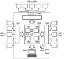
- FIG. 1 schematically shows a configuration of a laser annealing apparatus according to a comparative example.
- FIG. 2 shows a specific configuration of the laser apparatus shown in FIG.
- FIG. 3 shows the internal configuration of the laser chamber shown in FIG. 2 and the configuration of the pulse power module.
- FIG. 4 is a graph showing an example of the time waveform of the pulse laser beam output from the laser device.
- FIG. 5 schematically illustrates the configuration of the laser annealing apparatus according to the first embodiment of the present disclosure.
- FIG. 6A shows the configuration of the optical pulse stretcher shown in FIG.
- FIG. 6B shows a state in which the beam splitter is moved to a position different from that in FIG.
- FIG. 6A shows a state in which the posture of the concave mirror is different from that in FIG. 6A.
- FIG. 6C shows a state in which the posture of the concave mirror is different from that in FIG. 6B.
- FIG. 6D is a view of the beam splitter, the holder, the arm, the moving table, and the single-axis stage as seen from the direction perpendicular to the reflecting surface of the beam splitter.
- FIG. 6E shows a state in which the beam splitter is moved to a position different from that in FIG. 6D.
- FIG. 7 is a flowchart showing a setting process of a pulse time waveform by the annealing control unit shown in FIG. FIG.
- FIG. 8A is a flowchart showing details of processing for calculating a pulse time width while minimizing the reflectance of the beam splitter shown in FIG.
- FIG. 8B shows an example of a time waveform of pulsed laser light output from the optical pulse stretcher with the reflectance of the beam splitter set to the minimum.
- FIG. 9A is a flowchart showing details of processing for creating the irradiation condition parameter shown in FIG.
- FIG. 9B shows an example of a data structure when the irradiation condition parameters are stored in a table format.
- FIG. 10 is a flowchart showing details of a process for setting the laser system to the irradiation condition parameter shown in FIG.
- FIG. 11A is a flowchart showing details of a process for calculating the pulse parameters shown in FIG. FIG.
- FIG. 11B shows an example of a time waveform of the pulse laser beam output from the optical pulse stretcher.
- FIG. 12A is a flowchart showing details of the process for measuring the melting duration and the crystal state shown in FIG. 7.
- FIG. 12B shows an example of the change over time of the reflectance of the laser beam in the irradiation area of the workpiece.
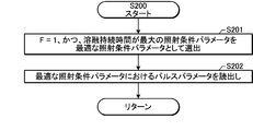
- FIG. 13 is a flowchart showing details of the process of selecting the optimum irradiation condition parameter shown in FIG.
- FIG. 14 shows the relationship between the fluence of pulsed laser light applied to the workpiece and the crystal grain size formed on the workpiece, and the relationship between the fluence of pulsed laser light applied to the workpiece and the melting duration. It is a graph which shows.
- FIG. 12A is a flowchart showing details of the process for measuring the melting duration and the crystal state shown in FIG. 7.
- FIG. 12B shows an example of the change over time of the reflectance of the laser beam in the irradiation area of the workpiece.
- FIG. 15 is a graph showing an example of a preferable pulse time waveform.
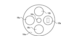
- FIG. 16A shows a configuration of an optical pulse stretcher used in a laser annealing apparatus according to the second embodiment of the present disclosure.
- FIG. 16B is a view of a plurality of beam splitters used in the optical pulse stretcher shown in FIG. 16A as viewed from a direction perpendicular to the reflecting surfaces of these beam splitters.
- FIG. 17A is a flowchart illustrating details of a process for selecting an optimum irradiation condition parameter in the laser annealing apparatus according to the third embodiment of the present disclosure.
- FIG. 17B shows an example of the relationship between melt duration and fluence.
- FIG. 18 schematically illustrates a configuration of a laser annealing apparatus according to the fourth embodiment of the present disclosure.
- FIG. 19 is a flowchart showing a pulse time waveform setting process by the annealing control unit shown in FIG.
- FIG. 20 is a flowchart showing details of processing for calculating the pulse time width of the pulse laser beam output from one laser unit shown in FIG.
- FIG. 21A is a flowchart showing details of a process for creating the irradiation condition parameter shown in FIG.
- FIG. 21B shows an example of a time waveform of pulsed laser light output from the laser system.
- FIG. 21C shows an example of a data structure when the irradiation condition parameters are stored in a table format.
- FIG. 22 is a flowchart illustrating an irradiation condition parameter setting process according to the fifth embodiment of the present disclosure.
- FIG. 23A is a flowchart showing a first example of processing for receiving the irradiation condition parameter shown in FIG.
- FIG. 23B is a flowchart illustrating a second example of the process of receiving the irradiation condition parameter illustrated in FIG.
- FIG. 24A is a flowchart illustrating a first example of processing for setting the received irradiation condition parameter shown in FIG.
- FIG. 24B is a flowchart showing a second example of processing for setting the received irradiation condition parameter shown in FIG.
- FIG. 25 is a block diagram illustrating a schematic configuration of the control unit.
- Laser annealing apparatus according to comparative example 2.1 Configuration of laser annealing apparatus 2.2 Operation of laser annealing apparatus 2.3 Details of laser apparatus 2.4 Problem 3.
- Laser annealing apparatus including an optical pulse stretcher (first embodiment) 3.1 Configuration 3.2 Operation 3.3 Configuration of Optical Pulse Stretcher 3.4 Operation of Optical Pulse Stretcher 3.5 Processing of Annealing Control Unit 3.5.1 Main Flow 3.5.2 Details of S100 3 5.3 Details of S110 3.5.4 Details of S130 3.5.5 Details of S150 3.5.6 Details of S160 3.5.7 Details of S200 3.6 Selection of irradiation conditions Variation of beam splitter (second embodiment) 5. Variation in selection of irradiation conditions (third embodiment) 6).
- Laser annealing apparatus including a plurality of laser units (fourth embodiment) 6.1 Configuration and Operation 6.2 Processing of Annealing Control Unit 6.2.1 Main Flow 6.2.2 Details of S100b 6.2.3 Details of S110b 6.3 Action 7.
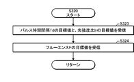
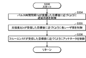
- Example of receiving irradiation condition parameters from external device 7.1 Main flow 7.2 Details of S320 (first example) 7.3 Details of S320 (second example) 7.4 Details of S330 (first example) 7.5 Details of S330 (second example) 8).
- the characteristics of the generated polycrystal can vary depending on the pulse time waveform of the pulsed laser beam output from the laser annealing apparatus. In the conventional laser annealing apparatus, it may be difficult to optimize the pulse time waveform of the pulse laser beam.
- the present disclosure relates to a laser annealing apparatus that varies a pulse time waveform of pulse laser light output from a laser system that is a light source of a laser annealing apparatus.
- FIG. 1 schematically shows a configuration of a laser annealing apparatus according to a comparative example.
- the laser annealing apparatus may include a laser system 3 and an annealing apparatus 4.
- the laser system 3 may include a laser device 2 and an attenuator 18.
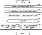
- the laser device 2 may be a laser device using any one of ArF, KrF, XeCl, and XeF as a laser medium.
- the attenuator 18 is disposed in the optical path of the pulsed laser light output from the laser device 2, and may include two partial reflection mirrors 18a and 18b and rotation stages 18c and 18d of these partial reflection mirrors. .
- the two partial reflection mirrors 18a and 18b may be optical elements whose transmittance varies depending on the incident angle of the pulse laser beam.
- the annealing apparatus 4 may include a slit 42, high reflection mirrors 43a and 43b, a transfer optical system 43d, a table 43f, and an XYZ stage 43g.
- the slit 42 may be disposed in the optical path of the pulse laser beam that has passed through the attenuator 18.
- the slit 42 may be arranged so that a region having a uniform light intensity distribution in the beam cross section of the pulsed laser light passes through.
- the high reflection mirrors 43a and 43b may be arranged so that the pulse laser beam that has passed through the slit 42 enters the transfer optical system 43d.
- the transfer optical system 43d may be an optical system including one or a plurality of convex lenses, or may be an optical system including one or a plurality of convex lenses and one or a plurality of concave lenses.
- the table 43f may support the workpiece 43e.
- the workpiece 43e may be formed by forming an amorphous silicon thin film on a glass substrate.
- the XYZ stage 43g may support the table 43f. The XYZ stage 43g may be adjusted so that a transfer image of the slit 42 is formed on the surface of the workpiece 43e on the table 43f.
- the two partial reflection mirrors 18a and 18b are configured so that the incident angles of the pulse laser light are substantially equal to each other, and the transmittance of the pulse laser light is a desired transmittance.
- the posture may be controlled by the rotary stages 18c and 18d. Thereby, the pulsed laser light output from the laser device 2 can be attenuated to a desired pulse energy and pass through the attenuator 18.
- the pulse laser beam that has passed through the attenuator 18 may pass through the slit 42 and enter the transfer optical system 43d via the high reflection mirrors 43a and 43b.
- the transfer optical system 43d can form a transfer image of the slit 42 on the workpiece 43e.
- pulsed laser light is irradiated to the workpiece 43e, and amorphous silicon in the irradiated region can be melted.
- the melted amorphous silicon can be crystallized after the irradiation with the pulsed laser beam is completed.
- FIG. 2 shows a specific configuration of the laser device shown in FIG. 2
- the laser device 2 shown in FIG. 2 may include a laser chamber 10, a pair of electrodes 11a and 11b, a charger 12, and a pulse power module (PPM) 13.
- PPM pulse power module
- FIG. 2 shows an internal configuration of the laser chamber 10 as viewed from a direction substantially perpendicular to the traveling direction of the laser light.
- the laser device 2 may further include a cross flow fan 21 and a motor 22.
- the laser device 2 may further include a high reflection mirror 14, an output coupling mirror 15, a pulse energy measurement unit 17, and a laser control unit 30.
- the laser chamber 10 may be a chamber in which the above-described laser medium is enclosed.
- the pair of electrodes 11a and 11b can be arranged in the laser chamber 10 as electrodes for exciting the laser medium by discharge.
- An opening may be formed in the laser chamber 10, and the opening may be closed by the electrical insulating unit 20.
- the electrode 11 a may be supported by the electrical insulating unit 20, and the electrode 11 b may be supported by the internal partition plate 10 c of the laser chamber 10.
- the electrically insulating portion 20 may be embedded with a conductive portion 20a.
- the conductive part 20a may electrically connect the high voltage terminal of the pulse power module 13 and the electrode 11a so that the high voltage supplied from the pulse power module 13 is applied to the electrode 11a.
- the rotation axis of the cross flow fan 21 may be connected to a motor 22 disposed outside the laser chamber 10.
- the laser gas may circulate inside the laser chamber 10 by the motor 22 rotating the cross flow fan 21.
- the charger 12 may be constituted by a capacitor connected to a power supply device, for example, and can hold electric energy for applying a high voltage between the pair of electrodes 11a and 11b.
- the pulse power module 13 may include a switch 13 a that is controlled by the laser control unit 30. When the switch 13a is turned from OFF to ON, the pulse power module 13 generates a pulsed high voltage from the electric energy held in the charger 12, and applies this high voltage between the pair of electrodes 11a and 11b. Also good.
- a discharge can occur between the pair of electrodes 11a and 11b. Due to the energy of this discharge, the laser medium in the laser chamber 10 can be excited to shift to a high energy level. When the excited laser medium subsequently moves to a low energy level, light having a wavelength corresponding to the energy level difference can be emitted.
- Windows 10 a and 10 b may be provided at both ends of the laser chamber 10.
- the light generated in the laser chamber 10 can be emitted to the outside of the laser chamber 10 through the windows 10a and 10b.
- the high reflection mirror 14 may reflect the light emitted from the window 10 a of the laser chamber 10 with a high reflectance and return it to the laser chamber 10.
- the surface of the output coupling mirror 15 may be coated with a partial reflection film. Therefore, the output coupling mirror 15 may transmit a part of the light output from the window 10 b of the laser chamber 10 and output it, and reflect the other part and return it to the laser chamber 10.
- the high reflection mirror 14 and the output coupling mirror 15 can constitute an optical resonator.
- the light emitted from the laser chamber 10 reciprocates between the high reflection mirror 14 and the output coupling mirror 15 and can be amplified every time it passes through the laser gain space between the electrode 11a and the electrode 11b. A part of the amplified light can be output as pulsed laser light via the output coupling mirror 15.
- the pulse energy measuring unit 17 may include a beam splitter 17a, a condensing optical system 17b, and an optical sensor 17c.
- the beam splitter 17a may transmit the pulsed laser light transmitted through the output coupling mirror 15 with high transmittance, and may reflect a part of the pulsed laser light toward the condensing optical system 17b.
- the condensing optical system 17b may condense the light reflected by the beam splitter 17a on the photosensitive surface of the optical sensor 17c.
- the optical sensor 17 c may detect the pulse energy of the laser light focused on the photosensitive surface and output the pulse energy detection data to the laser controller 30.
- the laser controller 30 may transmit, for example, a charging voltage setting signal to the charger 12 or a light emission trigger signal for switching ON or OFF to the pulse power module 13.
- the laser control unit 30 may receive pulse energy detection data from the pulse energy measurement unit 17, and may control the charging voltage of the charger 12 with reference to the pulse energy detection data.
- the pulse energy of the pulse laser beam may be controlled by controlling the charging voltage of the charger 12.
- the laser control unit 30 may count the number of oscillation pulses of the excimer laser device based on the data received from the pulse energy measurement unit 17.
- FIG. 3 shows the internal configuration of the laser chamber shown in FIG. 2 and the configuration of the pulse power module.
- FIG. 3 shows the internal configuration of the laser chamber 10 viewed from a direction substantially parallel to the traveling direction of the laser light.
- the conductive member including the internal partition plate 10c of the laser chamber 10 may be connected to the ground potential.
- the electrode 11b may be connected to the ground potential via the internal partition plate 10c.
- a heat exchanger 26 may be disposed inside the laser chamber 10. As the cross flow fan 21 rotates, the laser gas may circulate inside the laser chamber 10 as indicated by an arrow A. The heat exchanger 26 may discharge the thermal energy of the laser gas that has become a high temperature due to the discharge to the outside of the laser chamber 10.
- the pulse power module 13 may include a charging capacitor C0, a switch 13a, a step-up transformer TC1, a plurality of magnetic switches Sr1 to Sr3, and a plurality of capacitors C1, C2, and C3.
- any of the magnetic switches Sr1 to Sr3 may include a saturable reactor.
- Each of the magnetic switches Sr1 to Sr3 may have a low impedance when the time integration value of the voltage applied to both ends thereof reaches a predetermined value determined by the characteristics of each magnetic switch.
- a charging voltage may be set in the charger 12 by the laser control unit 30.
- the charger 12 may charge the charging capacitor C0 based on the set charging voltage.
- a light emission trigger signal may be input to the switch 13 a of the pulse power module 13 by the laser control unit 30. When the light emission trigger signal is input to the switch 13a, the switch 13a may be turned on. When the switch 13a is turned on, a current can flow from the charging capacitor C0 to the primary side of the step-up transformer TC1.
- the magnetic switch Sr1 When the time integral value of the voltage applied to the magnetic switch Sr1 reaches a threshold value, the magnetic switch Sr1 becomes magnetically saturated and the magnetic switch Sr1 can be closed. When the magnetic switch Sr1 is closed, a current flows from the secondary side of the step-up transformer TC1 to the capacitor C1, and the capacitor C1 can be charged.
- the magnetic switch Sr2 When the capacitor C1 is charged, the magnetic switch Sr2 eventually becomes magnetically saturated and the magnetic switch Sr2 can be closed. When the magnetic switch Sr2 is closed, a current flows from the capacitor C1 to the capacitor C2, and the capacitor C2 can be charged. At this time, the capacitor C2 may be charged with a pulse width shorter than the pulse width of the current when the capacitor C1 is charged.
- the magnetic switch Sr3 When the capacitor C2 is charged, the magnetic switch Sr3 eventually becomes magnetically saturated and the magnetic switch Sr3 can be closed. When the magnetic switch Sr3 is closed, a current flows from the capacitor C2 to the capacitor C3, and the capacitor C3 can be charged. At this time, the capacitor C3 may be charged with a pulse width shorter than the pulse width of the current when the capacitor C2 is charged.
- the pulse width of the current can be compressed and the voltage can be increased.
- the pulse laser beam may be output at a predetermined oscillation frequency.
- FIG. 4 is a graph showing an example of a time waveform of pulsed laser light output from a laser device.
- the ratio K is a value smaller than 1, the energy charged in the capacitor C3 is less than the energy charged in the capacitor C2, so that surplus energy can be generated. Then, after discharge occurs in the discharge electrodes 11a and 11b due to the energy charged in the capacitor C3, the discharge is reversed again due to the surplus energy, so that the pulse time width of the pulse laser beam can be increased.
- Japanese Patent Laid-Open No. 10-012950 discloses that a pulse time width suitable for annealing is realized by pulse stretching by this discharge.
- the pulse time waveform may fluctuate for each pulse depending on the change of the laser gas condition and the discharge state. If the pulse time waveform fluctuates, the characteristics of the polycrystal produced by annealing may change.
- US Patent Publication No. 2012/0260847 and US Patent No. 8737438 disclose that an optical pulse stretcher is used to increase the pulse time width. However, it may be difficult to optimize the pulse time waveform only by using an optical pulse stretcher.
- the reflectance of the beam splitter included in the optical pulse stretcher may be changeable.
- the optical path length of the delay optical path of the delay optical system included in the optical pulse stretcher may be changeable.
- 0.85 ⁇ K ⁇ 1.15 More preferably, 0.9 ⁇ K ⁇ 1.05
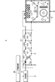
- FIG. 5 schematically illustrates the configuration of the laser annealing apparatus according to the first embodiment of the present disclosure.
- the laser system 3a includes an optical pulse stretcher 16, a pulse time waveform measuring unit 19, and a laser system control unit in addition to the laser system described with reference to FIG. 31 may be provided.
- the annealing apparatus 4a includes a beam homogenizer 41, a melt measurement unit 44, an annealing control unit 45, in addition to the annealing apparatus 4 described with reference to FIG. , May be provided.
- a high reflection mirror 43c may be arranged instead of the high reflection mirror 43b.
- the optical pulse stretcher 16 may be disposed in the optical path of the pulse laser beam between the laser device 2 and the attenuator 18.
- the optical pulse stretcher 16 may include a beam splitter and a delay optical system. Details of the optical pulse stretcher 16 will be described later with reference to FIGS. 6A to 6E.
- the pulse time waveform measuring unit 19 may be disposed in the optical path of the pulse laser beam between the attenuator 18 and the annealing device 4a.
- the pulse time waveform measurement unit 19 may include a beam splitter 19a, a condensing optical system 19b, and an optical sensor 19c.
- the beam splitter 19a may transmit the pulse laser beam that has passed through the attenuator 18 with high transmittance, and may reflect a part of the pulse laser beam toward the condensing optical system 19b.
- the condensing optical system 19b may condense the light reflected by the beam splitter 19a on the photosensitive surface of the optical sensor 19c.
- the optical sensor 19c may be a high-speed photodiode or a biplanar tube.
- the beam homogenizer 41 may be disposed in the optical path of the pulse laser beam between the pulse time waveform measuring unit 19 and the slit 42.
- the beam homogenizer 41 may include a fly-eye lens 41a and a condenser optical system 41b.
- the condenser optical system 41 b may be arranged so that the position of the rear focal point substantially coincides with the position of the slit 42.
- the fly-eye lens 41a may be arranged such that the position of the focal plane including the front focal point of the plurality of lenses included in the fly-eye lens 41a substantially coincides with the position of the front focal plane of the condenser optical system 41b.
- the high reflection mirror 43c may be a dichroic mirror that reflects the pulsed laser light in the ultraviolet region output from the laser device 2 with high reflectivity and transmits visible light.
- the melt measurement unit 44 may include a beam splitter 44a, a semiconductor laser 44b, and an optical sensor 44c.
- the semiconductor laser 44b may output laser light in the visible light region.
- the semiconductor laser 44b may be a semiconductor laser that outputs laser light having a wavelength of 1 ⁇ m to 660 nm.
- the beam splitter 44a may be a half mirror that reflects part of the laser light and transmits the other part.
- Part of the laser light output from the semiconductor laser 44b is reflected by the beam splitter 44a, passes through the high reflection mirror 43c, and is reflected by the workpiece 43e, and passes through the high reflection mirror 43c and the beam splitter 44a in this order. It may be transparent.
- the optical sensor 44c may be disposed in the optical path of the light that has passed through the high reflection mirror 43c and the beam splitter 44a in this order.
- the optical sensor 44c may be a photodiode having sensitivity to the wavelength of the laser light output from the semiconductor laser 44b.
- a band-pass filter that selectively transmits the wavelength of the laser beam output from the semiconductor laser 44b may be disposed in the optical path of the laser beam between the high reflection mirror 43c and the optical sensor 44c.
- the annealing control unit 45 may control the XYZ stage 43g so that the workpiece 43e is arranged at a predetermined position.
- the annealing control unit 45 transmits the data of the target pulse energy Et of the pulse laser beam that has passed through the attenuator 18 to the laser system control unit 31 so that the fluence of the pulse laser beam in the workpiece 43e becomes a predetermined value. Also good.
- T1 may be the transmittance of the optical pulse stretcher 16.
- the annealing control unit 45 may transmit a light emission trigger signal to the laser device 2 via the laser system control unit 31.
- a light emission trigger signal is input to the laser device 2
- a pulse laser beam having a pulse energy EL ⁇ b> 1 can be output from the laser device 2.
- the output pulsed laser light enters the optical pulse stretcher 16 and can be pulse stretched.
- the pulse-stretched pulse laser beam may be attenuated by the attenuator 18 so as to have a desired pulse energy. Thereafter, the pulsed laser light is partially reflected by the beam splitter 19a of the pulse time waveform measuring unit 19 and can enter the optical sensor 19c via the condensing optical system 19b.
- the laser system control unit 31 may receive a signal from the optical sensor 19c and measure the pulse time waveform of the pulse laser beam. Further, the pulse time waveform may be integrated to calculate the pulse energy to confirm whether the target pulse energy Et is reached. Further, the measured pulse time waveform data may be transmitted to the annealing control unit 45.
- the pulsed laser light that has passed through the pulse time waveform measuring unit 19 can be incident on the annealing device 4a.
- the pulse laser light incident on the annealing device 4 a can be Koehler illuminated at the slit 42 by the beam homogenizer 41.
- the light intensity distribution of the pulse laser beam can be made uniform.
- the pulse laser beam that has passed through the slit 42 is sequentially reflected by the high reflection mirrors 43a and 43c, and a transfer image of the slit 42 can be formed on the workpiece 43e by the transfer optical system 43d. Thereby, a part of the amorphous silicon can be melted and then crystallized in the workpiece 43e.
- the laser beam output from the semiconductor laser 44b of the melt measurement unit 44 is reflected by the beam splitter 44a, and the irradiation area of the pulse laser beam on the workpiece 43e via the high reflection mirror 43c and the transfer optical system 43d. Can be incident.
- the reflectance of the laser beam output from the semiconductor laser 44b can be changed in the process in which amorphous silicon is melted and then crystallized.
- the annealing control unit 45 may measure the time change of the light intensity of the reflected light of the laser beam output from the semiconductor laser 44b by the optical sensor 44c. And you may calculate the time change of the reflectance in the to-be-processed object 43e.
- the calculation of the reflectance may be performed in advance by arranging a sample having a high reflectance at the position of the workpiece and using the light intensity of the reflected light from the sample as a reference.
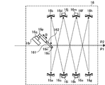
- FIG. 6A shows a configuration of the optical pulse stretcher shown in FIG.
- the optical pulse stretcher 16 may include a beam splitter 16n and concave mirrors 16a to 16h.
- the beam splitter 16n may include a substrate that transmits the pulsed laser light with high transmittance.
- the first surface 161 of the substrate may be coated with a reduced reflection film, and the second surface 162 of the substrate may be coated with a partial reflection film having a reflectance distribution in the arrow B direction.
- the beam splitter 16n may be supported by the arm 16p via the holder 16o.
- the arm 16p may be supported by the moving table 16q, and the moving table 16q may be supported by the uniaxial stage 16r.
- 6D and 6E are views of the beam splitter 16n, the holder 16o, the arm 16p, the moving table 16q, and the uniaxial stage 16r viewed from a direction perpendicular to the reflecting surface of the beam splitter 16n.
- 6B, 6C, and 6E show a state in which the beam splitter 16n and the like are moved to positions different from those in FIGS. 6A and 6D.
- the uniaxial stage 16r may be configured to reciprocate the beam splitter 16n, the holder 16o, the arm 16p, and the moving table 16q in the arrow B direction.
- the single axis stage 16r may be controlled by the laser system control unit 31 (FIG. 5). Thereby, the beam splitter 16n may be configured to be able to reciprocate in the direction of the arrow B while maintaining the incident angle of the pulse laser beam.
- the concave mirrors 16a to 16h can constitute a delay optical system.
- Each of the concave mirrors 16a to 16h may be a concave mirror having substantially the same focal length F.
- the concave mirrors 16c, 16d, 16e, and 16f may be supported by the rotary stages 16i, 16j, 16k, and 16m, respectively.
- the rotary stages 16i, 16j, 16k, and 16m may be configured such that the concave mirrors 16c, 16d, 16e, and 16f can be rotated in the plane of the paper to control their respective postures.
- the rotary stages 16i, 16j, 16k, and 16m may be controlled by the laser system control unit 31 (FIG. 5).
- the focal length F may correspond to, for example, the distance from the beam splitter 16n to the concave mirror 16a.
- the pulsed laser light incident on the beam splitter 16n from the left side in the drawing is transmitted through the first surface 161 with high transmittance and is incident on the partial reflection film on the second surface 162. obtain.
- the pulsed laser light incident on the second surface 162 can be branched into a first optical path and a second optical path. That is, a part of the pulsed laser light incident on the second surface 162 is transmitted, proceeds to the first optical path, and can become the first output pulse P1.
- the other part of the pulsed laser light incident on the second surface 162 is reflected, proceeds to the second optical path, and can be reflected by the concave mirror 16a.
- the pulse laser light reflected by the concave mirror 16a is in the order of the concave mirrors 16d, 16e, 16h, 16g, 16f, 16c, and 16b. And may enter the beam splitter 16n from the upper side in the drawing. A part of the pulsed laser light incident on the beam splitter 16n from the upper side in the figure is reflected and can travel to the first optical path to become the second output pulse P2. Another part of the pulsed laser light incident on the beam splitter 16n from the upper side in the drawing can pass through the beam splitter 16n and travel again to the second optical path.
- the first output pulse P1 that is incident on and transmitted through the beam splitter 16n from the left side in the figure and the second output pulse P2 that is incident on the beam splitter 16n and reflected from the upper side in the figure are substantially the same optical path axis. Thus, it can be output from the optical pulse stretcher 16 toward the right side in the figure.
- the optical path length of the delayed optical path that passes through the concave mirrors 16a, 16d, 16e, 16h, 16g, 16f, 16c, and 16b can correspond to 16 times the focal length F of each of the concave mirrors 16a to 16h.
- the delay time of the second output pulse P2 with respect to the first output pulse P1 can be 16 F / c, where c is the speed of light.
- the pulsed laser light that has entered the beam splitter 16n from the upper side in the drawing and has been transmitted is reflected again by the concave mirror 16a, passes through the same delay optical path as described above, and again enters the beam splitter 16n from the upper side in the drawing. Good.
- a part of the pulse laser beam incident on the beam splitter 16n again from the upper side in the figure can be reflected and output from the optical pulse stretcher 16 toward the right side in the figure.
- third and fourth output pulses may be output on the optical path axes substantially the same as the first and second output pulses P1 and P2, and the pulse laser beam may be pulse stretched.
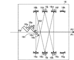
- FIG. 6B shows a state in which the postures of the concave mirrors 16c, 16d, 16e, and 16f are different from those in FIG. 6A.
- the pulse laser light reflected by the concave mirror 16a is reflected in the order of the concave mirrors 16d, 16e, 16f, 16c, and 16b.
- the concave mirrors 16h and 16g may be skipped.
- the optical path length of the delay optical path may correspond to about 12 times the focal length F of each of the concave mirrors 16a to 16h.
- FIG. 6C shows a state in which the postures of the concave mirrors 16c, 16d, 16e, and 16f are different from those in FIGS. 6A and 6B.
- the pulsed laser light reflected by the concave mirror 16a may be reflected in the order of the concave mirrors 16d, 16c, and 16b. That is, the concave mirrors 16e, 16h, 16g, and 16f may be skipped.
- the optical path length of the delay optical path may correspond to about 8 times the focal length F of each of the concave mirrors 16a to 16h.
- the optical path length of the delay optical path can be varied to 8F, 12F, and 16F depending on the posture of the concave mirrors 16c, 16d, 16e, and 16f.
- a transfer image of the beam cross section of the pulsed laser light incident on the second surface 162 of the beam splitter 16n from the left side in the drawing can be formed on the second surface 162 of the beam splitter 16n.
- the delay time of the second output pulse P2 with respect to the first output pulse P1 and the third and fourth output pulses described above can be changed.
- the time waveform of the pulse laser beam to be applied can be changed.
- the rotary stages 16i, 16j, 16k, and 16m may correspond to the optical path length variable unit in the present disclosure.
- the reflectance of the pulsed laser light at the beam splitter 16n can be changed by the reciprocating movement of the single-axis stage 16r in the direction of arrow B through the position of the beam splitter 16n.
- the intensity ratio of the second output pulse P2 and the third and fourth output pulses to the first output pulse P1 can be changed by changing the reflectance of the pulsed laser light in the beam splitter 16n, so that the optical pulse stretcher
- the time waveform of the pulse laser beam output from 16 can be changed.
- the uniaxial stage 16r may correspond to the reflectivity variable unit in the present disclosure.
- the pulse time intervals of the first to fourth output pulses and the first to fourth output pulses can be changed.
- the light intensity ratio of the output pulse can be changed.
- the optical pulse stretcher 16 may correspond to the pulse time waveform variable device in the present disclosure.
- FIGS. 6A to 6E show examples using eight concave mirrors, the present disclosure is not limited to this example, and more concave mirrors may be arranged in the same manner. Other points may be the same as those of the laser annealing apparatus described with reference to FIGS.
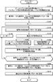
- FIG. 7 is a flowchart showing setting processing of a pulse time waveform by the annealing control unit shown in FIG.
- the annealing control unit 45 may perform annealing under a plurality of irradiation conditions by the following processing, measure the melted state under each irradiation condition, and select an optimal irradiation condition.
- the annealing control unit 45 may calculate the pulse time width by measuring the time waveform of the pulsed laser light while minimizing the reflectance of the beam splitter 16n. Thereby, a waveform close to the time waveform of the pulse laser beam before being output from the laser device 2 and entering the optical pulse stretcher 16 can be acquired. Details of this processing will be described later with reference to FIGS. 8A and 8B.
- the memory will be described later with reference to FIG.
- the irradiation condition parameters are Nmax as to the target value of the optical path length of the delay optical path of the optical pulse stretcher 16, the target value of the reflectivity of the beam splitter 16n, and the target value of the fluence of the pulse laser beam in the workpiece 43e. May be included. Details of the processing in S110 will be described later with reference to FIG. 9A.
- the irradiation condition parameter may be stored in the form of a data table to be described later with reference to FIG. 9B.
- the irradiation condition parameter may include a pulse time waveform generation parameter and a target value of the fluence in the workpiece 43e.
- the pulse time waveform generation parameter is a parameter necessary for generating the pulse time waveform.
- the target value of the reflectance of the beam splitter 16n and the target of the optical path length of the delay optical path of the optical pulse stretcher 16 are used. And a value.
- the annealing control unit 45 may set the value of the number N to 1.
- the annealing control unit 45 may set the laser system 3a as the irradiation condition parameter of number N. That is, the annealing control unit 45 performs laser system control on the target value of the optical path length of the delay optical path of the optical pulse stretcher 16, the target value of the reflectance of the beam splitter 16n, and the target value of the fluence in the workpiece 43e. You may transmit to the part 31. Details of this processing will be described later with reference to FIG. Next, in S ⁇ b> 140, the annealing control unit 45 may output a light emission trigger signal to the laser system control unit 31.
- the annealing control unit 45 may advance the process to S150 and S160.
- the processes of S150 and S160 may be performed in parallel.
- the annealing control unit 45 may measure the time waveform of the pulse laser beam output from the optical pulse stretcher 16 by the pulse time waveform measurement unit 19 and calculate the pulse parameter.
- the pulse parameter is a value calculated from the time waveform of the pulse laser beam measured by the pulse time waveform measuring unit 19, and may include the following values.
- Ip1, Ip2, Ip3 first to third peak light intensity
- Td peak interval ⁇ T
- TIS [ ⁇ I (t) dt] 2 / ⁇ I (t) pulse time width calculated by 2 dt
- the pulse parameters Details of the calculation processing will be described later with reference to FIGS. 11A and 11B.
- the annealing control unit 45 determines the melting duration Tm of the workpiece 43e based on the time change of the reflectance of the laser beam in the irradiation region of the workpiece 43e measured using the optical sensor 44c, the crystal The state may be measured.
- the measurement of the crystal state may include measurement of the presence or absence of crystallization. Details of this processing will be described later with reference to FIGS. 12A and 12B.
- the annealing control unit 45 may advance the process to S170.
- the annealing control unit 45 may store the measurement results in S ⁇ b> 150 and S ⁇ b> 160 in the memory regarding the irradiation condition parameter of number N. This measurement result may be stored in the form of a data table to be described later with reference to FIG. 9B.
- the annealing control unit 45 may set the laser system 3a to the selected irradiation condition parameter. That is, the target value of the optical path length of the delay optical path of the optical pulse stretcher 16, the target value of the reflectance of the beam splitter 16n, and the target value of the fluence in the workpiece 43e are transmitted to the laser system control unit 31. Also good. This process may be the same as S130 described above except that the irradiation condition parameter number may be different.
- the annealing control unit 45 may end the process of this flowchart. Alternatively, the annealing control unit 45 may set a plurality of finer irradiation conditions in the vicinity of the selected irradiation condition and execute the process of this flowchart again.
- FIG. 8A is a flowchart showing details of processing for calculating the pulse time width while minimizing the reflectivity of the beam splitter shown in FIG.
- the process shown in FIG. 8A may be performed by the annealing control unit 45 as a subroutine of S100 shown in FIG.
- the annealing control unit 45 may set the reflectance of the beam splitter 16n to the minimum.
- the reflectance of the beam splitter 16n may be set by moving the beam splitter 16n under the control of the uniaxial stage 16r.
- the annealing control unit 45 may output a light emission trigger signal to the laser system control unit 31.
- the annealing control unit 45 may measure the time waveform of the pulse laser light output from the optical pulse stretcher 16 by the pulse time waveform measurement unit 19.
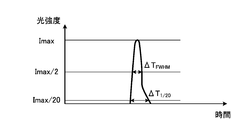
- the annealing control unit 45 may calculate the following pulse time width from the measured time waveform of the pulsed laser light.
- ⁇ T FWHM Full width at half maximum
- ⁇ T 1/20 Full width at 5%
- FIG. 8B shows an example of a time waveform of pulsed laser light output from the optical pulse stretcher with the reflectance of the beam splitter set to the minimum.
- the above-described ⁇ T FWHM may be a pulse time width of a portion where the light intensity is Imax / 2.
- the above ⁇ T 1/20 may be a pulse time width of a portion where the light intensity is Imax / 20.
- the annealing control unit 45 may end the process of this flowchart.
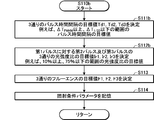
- FIG. 9A is a flowchart showing details of processing for creating the irradiation condition parameters shown in FIG. The process shown in FIG. 9A may be performed by the annealing control unit 45 as a subroutine of S110 shown in FIG.
- the annealing control unit 45 may determine three optical path lengths L1, L2, and L3 of the delay optical path of the optical pulse stretcher 16.
- the optical path length of the delay optical path may be selected in the range where the delay time of the pulsed laser light passing through the delay optical path is not less than ⁇ T FWHM and not more than ⁇ T 1/20 .
- the annealing control unit 45 may determine three reflectances R1, R2, and R3 of the beam splitter 16n.
- the reflectance of the beam splitter 16n may be selected, for example, in the range of 25% or more and 65% or less. If the reflectivity of the beam splitter 16n is less than 25%, the effect of pulse stretching is not sufficient, and peaks after the second peak described later with reference to FIG. 11B may not appear. When the reflectivity of the beam splitter 16n exceeds 65%, the intensity ratio of the second peak light intensity to the first peak light intensity described later with reference to FIG. 11B exceeds 75%, and an ideal pulse time waveform is obtained. It may not be.
- the annealing control unit 45 may determine the three fluence target values F1, F2, and F3 of the pulse laser beam in the workpiece 43e.
- the target value of the fluence of the pulsed laser beam in the workpiece 43e may be determined so that at least a part of the workpiece 43e is melted.
- the annealing control unit 45 may store the irradiation condition parameters determined in S111 to S113 in the memory.
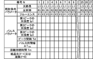
- FIG. 9B shows an example of a data structure when the irradiation condition parameters are stored in a table format.
- each of the target value of the optical path length of the delay optical path of the optical pulse stretcher 16, the target value of the reflectivity of the beam splitter 16n, and the target value of the fluence of the pulsed laser light on the workpiece 43e is 3 respectively.
- the irradiation condition parameter can be 27 types.
- measurement results for each of the 27 irradiation condition parameters may be stored in the table shown in FIG. 9B.
- the irradiation condition parameters are not limited to 27, and may be two or more.
- the annealing control unit 45 may end the process of this flowchart.
- FIG. 10 is a flowchart showing details of processing for setting the laser system to the irradiation condition parameter shown in FIG.
- the processing shown in FIG. 10 may be performed by the annealing control unit 45 as a subroutine of S130 shown in FIG.
- the annealing control unit 45 may read the irradiation condition parameter of number N.
- the annealing control unit 45 may set the laser system 3a to the read irradiation condition parameter.
- the laser system control unit 31 of the laser system 3 a may receive the irradiation condition parameter from the annealing control unit 45.
- the laser system control unit 31 rotates the concave mirrors 16c, 16d, 16e, and 16f of the optical pulse stretcher 16 so that the optical path length of the delay optical path of the optical pulse stretcher 16 approaches the target value, respectively. , 16k, 16m may be controlled.
- the laser system control unit 31 may control the uniaxial stage 16r that moves the beam splitter 16n so that the reflectance of the beam splitter 16n approaches the target value.
- the laser system control unit 31 may control the transmittance of the attenuator 18 so that the fluence of the workpiece 43e approaches the target value.
- the attenuator 18 may correspond to the fluence variable unit in the present disclosure.
- the annealing control unit 45 may end the process of this flowchart.
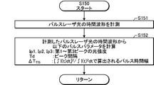
- FIG. 11A is a flowchart showing details of processing for calculating the pulse parameters shown in FIG.
- the process shown in FIG. 11A may be performed by the annealing control unit 45 as a subroutine of S150 shown in FIG.
- the annealing control unit 45 may measure the time waveform of the pulse laser beam output from the optical pulse stretcher 16 by the pulse time waveform measuring unit 19.
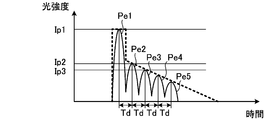
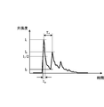
- FIG. 11B shows an example of the time waveform of the pulsed laser beam output from the optical pulse stretcher.
- the largest light intensity in the waveform shown in FIG. 11B is the first peak Pe1 configured by the first output pulse P1 (FIG. 6A) that has entered the beam splitter 16n and transmitted from the left side in FIG. 6A. There may be.
- the waveform shown in FIG. 11B may include, in addition to the first peak Pe1, a second peak Pe2 composed of the second output pulse P2 that is incident on the beam splitter 16n and reflected from the upper side in FIG. 6A. .
- the light intensity Ip2 of the second peak Pe2 may be smaller than the light intensity Ip1 of the first peak Pe1.
- the third output pulse that is incident on and transmitted through the beam splitter 16n from the upper side in FIG. 6A and is incident on the beam splitter 16n again from the upper side in FIG. 6A and then reflected may constitute the third peak Pe3. .
- the light intensity Ip3 of the third peak Pe3 may be smaller than the light intensity Ip2 of the second peak Pe2.
- the time difference between the first peak Pe1 and the second peak Pe2 may be measured as the peak interval Td.
- the time difference between the second peak Pe2 and the third peak Pe3 may be approximately equal to the peak interval Td. That is, when the optical path length of the delay optical path is L, the peak interval Td can be L / c, where c is the speed of light.
- the reason why the light intensity Ip1 of the first peak Pe1 is increased may be to give energy for melting the workpiece to the workpiece by the first peak Pe1.
- the light intensity Ip1 of the first peak Pe1 is preferably not too high.
- the reason why the light intensity after the second peak Pe2 may be smaller than the light intensity Ip1 of the first peak Pe1 may be that the melted state of the workpiece may be maintained after the second peak Pe2.
- the annealing control unit 45 may calculate the following pulse parameters from the measured time waveform of the pulse laser beam.
- Td peak interval ⁇ T
- TIS [ ⁇ I (t) dt] 2 / ⁇ I (t) pulse time widths calculated by 2 dt
- the annealing control unit 45 may end the process of this flowchart.
- FIG. 12A is a flowchart showing details of the process for measuring the melting duration and the crystal state shown in FIG.
- the process shown in FIG. 12A may be performed by the annealing control unit 45 as a subroutine of S160 shown in FIG.
- the annealing control unit 45 may measure a temporal change in the reflectance of the laser beam in the irradiation region of the workpiece 43e. Specifically, the annealing control unit 45 measures the light intensity of the reflected light of the laser light reflected by the irradiation region of the workpiece 43e by the optical sensor 44c, and based on the light intensity of the reflected light, the reflectance You may measure the time change of.
- FIG. 12B shows an example of the change over time of the reflectance of the laser beam in the irradiation area of the workpiece.
- the reflectance can be about 40% before the workpiece 43e is irradiated with pulsed laser light.
- the irradiation region of the workpiece 43e starts to melt.
- the irradiation region of the workpiece 43e has a solid portion and a liquid portion, the surface shape of the irradiation region of the workpiece 43e becomes complicated, and the reflectance may be temporarily reduced.
- the surface shape of the irradiation area of the workpiece 43e is flattened, and the reflectance becomes higher than before irradiation with the pulse laser beam, which is about 70%. Can be.
- the irradiation area of the workpiece 43e starts to solidify.
- the surface shape of the irradiation area of the workpiece 43e becomes complicated, and the reflectance may be lowered.
- the reflectance can be the same as that before irradiation with the pulse laser beam. If the irradiation region of the workpiece 43e is not crystallized, aggregation occurs in the irradiation region of the workpiece 43e, the surface shape becomes complicated, and the pulse laser beam is scattered.
- the reflectivity is lower and can be about 10%.
- the annealing control unit 45 may calculate the melting duration Tm from the change in reflectance over time.
- the melting duration Tm may be calculated as a time during which the state in which the reflectance is higher than the first threshold value Rth1 is continued.
- the first threshold Rth1 may be about 55%, for example.
- the annealing control unit 45 may calculate the reflectance Rs after solidification from the change in reflectance over time.
- the reflectivity after solidification may be calculated as the reflectivity when a certain time has elapsed after the end of the melting duration Tm.
- the annealing control unit 45 may determine whether the reflectivity Rs after solidification is equal to or greater than the second threshold Rth2.
- the second threshold Rth2 may be a value smaller than the first threshold Rth1.
- the second threshold Rth2 may be about 25%, for example.
- the annealing control unit 45 determines that the irradiation region of the workpiece 43e has crystallized, and the determination result is determined.
- a flag may be set. Specifically, the value of the variable F may be set to 1. If the reflectivity Rs after solidification is not greater than or equal to the second threshold Rth2 (S164; NO), in S166, the annealing control unit 45 determines that the irradiation region of the workpiece 43e is not crystallized, and the determination result May be set. Specifically, the value of the variable F may be set to 0.
- the annealing control unit 45 may end the process of this flowchart.
- FIG. 13 is a flowchart showing details of the process of selecting the optimum irradiation condition parameter shown in FIG.
- the process shown in FIG. 13 may be performed by the annealing control unit 45 as a subroutine of S200 shown in FIG.
- the reason for selecting the irradiation condition parameter with the longest melting duration will be described later with reference to FIG.
- the annealing control unit 45 may read out the pulse parameter in the optimum irradiation condition parameter from the data stored in S170 described above.
- the annealing control unit 45 may end the process of this flowchart.
- FIG. 14 shows the relationship between the fluence of pulsed laser light irradiated on the workpiece and the crystal grain size formed on the workpiece, and the fluence of pulsed laser light irradiated on the workpiece. It is a graph which shows the relationship between a melting duration.
- FIG. 14 shows the measurement results when the optical pulse stretcher is not used and the measurement results when the optical pulse stretcher is used as described with reference to FIGS. 5 and 6A to 6E. Yes.
- the melting duration can be increased.
- the fluence of the pulse laser beam is increased and the melting duration is increased, the workpiece is damaged, and a preferable large particle size tends not to be obtained.
- an optical pulse stretcher is used to irradiate the workpiece with pulsed laser light having second and third peaks whose light intensity is lower than that of the first peak. Then, by selecting the irradiation conditions for crystallization of the workpiece and the maximum melting duration, it is possible to obtain polycrystalline silicon having a large particle size.
- FIG. 15 is a graph showing an example of a preferable pulse time waveform.
- the pulse time waveform shown in FIG. 15 may include a first peak, a second peak, and a third peak.
- the light intensity I 1 of the first peak 36 mW / cm 2 or more, preferably 90MW / cm 2 or less.
- the minimum intensity I 2 between the first peak and the second peak is preferably 13 MW / cm 2 or more and not more than the light intensity of the second peak.
- the ratio of the second peak light intensity I 3 to the first peak light intensity I 1 is preferably 74% or less.
- the time difference T 4 between the first peak and the second peak is preferably 12 ns or more and 100 ns or less, or the full width at half maximum of the first peak and the full width of 5% of the first peak.
- the full width at half maximum T5 of the first peak is preferably 15 ns or more and 50 ns or less.
- FIG. 16A shows a configuration of an optical pulse stretcher used in a laser annealing apparatus according to the second embodiment of the present disclosure.
- FIG. 16B is a view of a plurality of beam splitters used in the optical pulse stretcher shown in FIG. 16A as viewed from a direction perpendicular to the reflecting surfaces of these beam splitters.
- the optical pulse stretcher 16z used in the second embodiment may include a plurality of beam splitters 16s, 16t, 16u, and 16v.
- the plurality of beam splitters 16s, 16t, 16u, and 16v may have different reflectances.
- the plurality of beam splitters 16s, 16t, 16u, and 16v may be supported by a holder 16w, and the holder 16w may be rotatably supported by a step motor 16x.
- the laser system control unit 31 may selectively arrange the beam splitters 16s, 16t, 16u, and 16v in the optical path of the pulsed laser light by controlling the step motor 16x. Even when any of the beam splitters 16s, 16t, 16u, and 16v is located in the optical path of the pulse laser beam, the incident angle of the pulse laser beam may be constant and only the reflectance may be different from each other. Thereby, the time waveform of the pulse laser beam output from the optical pulse stretcher 16z can be changed.
- the step motor 16x may correspond to the reflectivity variable unit in the present disclosure. About another point, it may be the same as that of 1st Embodiment.
- FIG. 17A is a flowchart illustrating details of a process for selecting an optimum irradiation condition parameter in the laser annealing apparatus according to the third embodiment of the present disclosure.
- the configuration of the laser annealing apparatus according to the third embodiment may be the same as the configuration of the laser annealing apparatus according to the first or second embodiment.
- the process shown in FIG. 17A may be performed by the annealing control unit 45 as a subroutine of S200 shown in FIG.
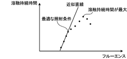
- the relationship between the fluence of the pulsed laser light applied to the workpiece and the melting duration is approximately parallel to the straight line B and increases as the fluence increases. It may include portions where the melting duration is increased.
- the relationship between the fluence and the melting duration can be separated from the straight line B, and the melting duration can be shortened. And just before the relationship between the fluence and the melting duration departs from the straight line B, the crystal grain size can be almost maximized.
- an optimal irradiation condition parameter may be selected by the following processing.
- the annealing control unit 45 selects a plurality of irradiation condition parameters in which the selected irradiation condition parameter and the pulse time waveform generation parameter are the same, and the selected irradiation condition parameter is different from the fluence target value.
- the data stored in S110 (FIG. 7) may be read out.
- the annealing control unit 45 may read the melting durations in the plurality of read irradiation condition parameters from the data stored in S170 described above, and obtain the relationship between the melting duration and the fluence. That is, the relationship between the melting duration and the fluence when the fluence is changed by fixing the pulse time waveform generation parameter of the selected irradiation condition parameter may be obtained.
- the annealing control unit 45 may obtain an approximate straight line from the relationship between the melting duration and the fluence.
- FIG. 17B shows an example of the relationship between melt duration and fluence.
- the annealing control unit 45 may obtain an approximate line as shown in FIG. 17B. This approximate straight line may be obtained for a region where the fluence is smaller than the portion where the melting duration is maximum.
- the annealing control unit 45 may select an irradiation condition parameter that is on or near the approximate line and has the maximum melting duration as the optimum irradiation condition parameter.
- the annealing control unit 45 may read out the pulse parameter in the optimum irradiation condition parameter from the data stored in S170 described above.
- the annealing control unit 45 may end the process of this flowchart.
- the other points may be the same as the processing described with reference to FIGS.
- the number of fluence samples is preferably larger than three.
- the number of fluence samples is preferably about 4 to 10.
- conditions for increasing the crystal grain size can be extracted from the relationship between fluence and melting duration. Therefore, a polycrystalline silicon film better than that in the first or second embodiment can be formed.
- FIG. 18 schematically illustrates a configuration of a laser annealing apparatus according to the fourth embodiment of the present disclosure.
- the laser system 3b includes first, second, and third laser units 2a, 2b, and 2c, a delay circuit 5, high reflection mirrors 6a and 6b, and a knife edge. Mirrors 6c and 6d may be provided.
- the laser system 3b may not include the optical pulse stretcher. The other points may be the same as the configurations of the first to third embodiments.
- Each of the first, second, and third laser units 2a, 2b, and 2c may have the same configuration as the laser device 2 described above.
- Each laser unit may receive target pulse energy data from the laser system control unit 31.
- the target pulse energy data may be different between the first, second, and third laser units 2a, 2b, and 2c.
- the charging voltage of the charging capacitor C0 by the charger 12 may be set by the laser control unit 30 based on the received target pulse energy data.
- the delay circuit 5 may receive delay time setting data from the laser system control unit 31.
- the delay circuit 5 may receive the light emission trigger signal output from the annealing control unit 45 via the laser system control unit 31.
- the delay circuit 5 emits light to each of the first, second, and third laser units 2a, 2b, and 2c in this order at a timing when a set delay time has elapsed since the reception of the light emission trigger signal.
- a trigger signal may be output.
- the high reflection mirror 6a and the knife edge mirror 6c may change the optical path by reflecting the pulse laser beam output from the first laser unit 2a with a high reflectance.
- the pulse laser beam output from the first laser unit 2a and whose optical path has been changed may be output toward the attenuator 18 substantially in parallel with and close to the pulse laser beam output from the second laser unit 2b. Good.
- the high reflection mirror 6b and the knife edge mirror 6d may change the optical path by reflecting the pulse laser beam output from the third laser unit 2c with a high reflectance.
- the pulse laser beam whose optical path is changed by being output from the third laser unit 2c may be output toward the attenuator 18 substantially in parallel with and close to the pulse laser beam output from the second laser unit 2b. Good.
- the pulse laser beams output from the first, second, and third laser units 2a, 2b, and 2c may enter the beam homogenizer 41 via the attenuator 18 and the pulse time waveform measurement unit 19.
- the slit 42 is Koehler-illuminated by the beam homogenizer 41, the optical paths of these pulsed laser beams overlap at the slit 42, and the light intensity profile of the beam at the opening of the slit 42 can be made uniform.
- FIG. 19 is a flowchart showing setting processing of a pulse time waveform by the annealing control unit shown in FIG.
- the annealing control unit 45 may select optimal irradiation conditions by the following processing.
- the annealing control unit 45 may measure the time waveform of the pulse laser beam output from one laser unit and calculate the pulse time width. Details of this processing will be described later with reference to FIG.
- the memory will be described later with reference to FIG.
- the irradiation condition parameters are the target value of the pulse time interval of the pulse laser beam output from the first, second, and third laser units 2a, 2b, and 2c, and the first, second, and third laser units 2a, Nmax combinations of the target value of the light intensity ratio of the pulsed laser light output from 2b and 2c and the target value of the fluence of the pulsed laser light in the workpiece 43e may be included. Details of this processing will be described later with reference to FIGS. 21A and 21B.
- the irradiation condition parameter may be stored in the form of a data table to be described later with reference to FIG. 21C.
- the irradiation condition parameter may include a pulse time waveform generation parameter and a target value of the fluence of the workpiece.
- the pulse time waveform generation parameter includes the target value of the pulse time interval of the pulse laser light output from the first, second, and third laser units 2a, 2b, and 2c, and the first, second, and third parameters. And a target value of the light intensity ratio of the pulse laser beam output from the laser units 2a, 2b, and 2c.
- the processing after S120 may be the same as the processing in the first to third embodiments.
- the target pulse energy data of each of the first, second, and third laser units 2a, 2b, and 2c is converted into a laser system. It may be set by the control unit 31.
- the charging voltage of the charging capacitor C0 by the charger 12 may be set so that the pulse energy of the pulse laser beam output from each laser unit approaches each target pulse energy. As a result of setting the charging voltage in this way, the light intensity ratio of the pulse laser light output from each laser unit may approach the target value of the light intensity ratio.
- the setting data of the delay time of the light emission trigger signal for each of the first, second, and third laser units 2a, 2b, and 2c may be set by the laser system control unit 31.
- the delay time may be set so that the pulse time interval of the pulse laser beam output from each of the first, second, and third laser units 2a, 2b, and 2c approaches the target value.
- FIG. 20 is a flowchart showing details of a process for calculating the pulse time width of the pulse laser beam output from one laser unit shown in FIG.
- the process shown in FIG. 20 may be performed by the annealing control unit 45 as a subroutine of S100b shown in FIG.
- the annealing control unit 45 may output a light emission trigger signal for output to the first laser unit 2a to the laser system control unit 31.
- the annealing control unit 45 may measure the time waveform of the pulse laser beam by the pulse time waveform measurement unit 19.
- the annealing control unit 45 may calculate the following pulse time width from the measured time waveform of the pulsed laser light.
- ⁇ T FWHM Full width at half maximum
- ⁇ T 1/20 Full width at 5%
- These pulse time widths may be the same as those in the first embodiment.
- the annealing control unit 45 may end the process of this flowchart.
- FIG. 21A is a flowchart showing details of processing for creating the irradiation condition parameters shown in FIG. The process shown in FIG. 21A may be performed by the annealing control unit 45 as a subroutine of S110b shown in FIG.
- the annealing control unit 45 sets the target values Td1, Td2, and Td3 of the three pulse time intervals of the pulse laser light output from the first, second, and third laser units 2a, 2b, and 2c. You may decide.
- the target value of the pulse time interval may be determined so as to be in a range of ⁇ T FWHM or more and ⁇ T 1/20 or less.
- the annealing control unit 45 performs three types of pulse laser beams output from the second and third laser units 2b and 2c with respect to the peak intensity of the pulse laser beam output from the first laser unit 2a.
- the target values Ir1, Ir2, and Ir3 of the light intensity ratio may be determined.
- the target value of the light intensity ratio may be determined to be in the range of 10% or more and 75% or less, for example.
- FIG. 21B shows an example of the time waveform of the pulsed laser beam output from the laser system 3b.
- the second pulse output from the second laser unit 2b may have a delay of the pulse time interval Td with respect to the first pulse output from the first laser unit 2a.
- the third pulse output from the third laser unit 2c may have a delay of the pulse time interval Td with respect to the second pulse output from the second laser unit 2b.
- the light intensity Ip2 may have a light intensity ratio Ir.
- the intensity Ip3 may have a light intensity ratio Ir.
- the light intensity Ip2 of the second peak and the light intensity Ip3 of the third peak may be substantially the same.
- the annealing control unit 45 may determine the target values F1, F2, and F3 of the three fluences of the pulse laser beam in the workpiece 43e.
- the target value of the fluence of the pulsed laser beam in the workpiece 43e may be determined so that at least a part of the workpiece 43e is melted.
- the annealing control unit 45 may store the irradiation condition parameters determined in S111b to S113 in the memory.
- FIG. 21C shows an example of a data structure when the irradiation condition parameters are stored in a table format.
- the target value of the pulse time interval of the pulse laser beam output from the first, second, and third laser units 2a, 2b, and 2c, and the first, second, and third laser units 2a When three values are determined for the target value of the light intensity ratio of the pulsed laser light output from 2b and 2c and the target value of the fluence of the pulsed laser light at the workpiece 43e, the irradiation condition parameter Can be 27 ways. In the table shown in FIG.
- the measurement results for each of the 27 irradiation condition parameters may be stored in the table shown in FIG. 21C.
- the irradiation condition parameters are not limited to 27, and may be two or more.
- the annealing control unit 45 may end the process of this flowchart.
- the output timing of the pulsed laser light from the plurality of laser units can be set by the delay circuit 5. Further, the light intensity ratio of the pulsed laser light by the plurality of laser units can be set by the charging voltage of the charging capacitor C0 by the charger 12 of each laser unit. Therefore, the delay circuit 5 and the charger 12 of the laser unit can correspond to the pulse time waveform variable device in the present disclosure. According to the fourth embodiment, it is possible to individually set the output timing and the light intensity ratio of the pulse laser light from the plurality of laser units. Therefore, the degree of freedom of the time waveform of the pulse laser beam obtained by superimposing these pulse laser beams can be improved as compared with the first to third embodiments.
- FIG. 22 is a flowchart showing an irradiation condition parameter setting process according to the fifth embodiment of the present disclosure.
- the annealing control unit 45 may receive the irradiation condition parameter input from the external device and set the irradiation condition parameter by the following process. The measurement by the melt measurement unit 44 may not be performed.
- the annealing control unit 45 may determine whether or not an irradiation condition parameter is input from an external device.
- the external device may be a computer system connected via a network, for example.
- the external device may be an input device such as a keyboard or a touch panel display.
- the annealing control unit 45 may wait until the irradiation condition parameter is input.
- the annealing control unit 45 may advance the process to S320.
- the annealing control unit 45 may receive the input irradiation condition parameter. This process will be described later with reference to FIGS. 23A and 23B.
- the annealing control unit 45 may set various apparatuses for the received irradiation condition parameter. This process will be described later with reference to FIGS. 24A and 24B.
- the annealing control unit 45 may output a light emission trigger signal to the laser system control unit 31. Accordingly, the workpiece may be irradiated with pulsed laser light.
- the annealing control unit 45 may determine whether or not the irradiation condition parameter has been changed.
- the annealing control unit 45 may return the process to the above-described S310 and receive the irradiation condition parameter again.
- the annealing control unit 45 may advance the process to S360.
- the annealing control unit 45 may determine whether or not to stop the irradiation with the pulse laser beam. When the irradiation with the pulse laser beam is not stopped (S360; NO), the annealing control unit 45 may return the process to the above-described S340 and repeat the output of the light emission trigger signal. When the irradiation of the pulse laser beam is stopped (S360; YES), the annealing control unit 45 may end the process of this flowchart.
- FIG. 23A is a flowchart showing a first example of processing for receiving the irradiation condition parameter shown in FIG.
- the process shown in FIG. 23A may be performed by the annealing control unit 45 as a subroutine of S320 shown in FIG.
- the process shown in FIG. 23A may be executed in the configuration in which the irradiation condition is changed by the control of the optical pulse stretcher 16 described in the first or second embodiment.
- the annealing control unit 45 may receive the target value of the reflectance R of the beam splitter 16n and the target value of the optical path length L of the delay optical path, respectively.
- the annealing control unit 45 may receive the target value of the fluence F. After S322, the annealing control unit 45 may end the process of this flowchart and proceed to S330 in FIG.
- FIG. 23B is a flowchart illustrating a second example of the process of receiving the irradiation condition parameter illustrated in FIG.
- the process shown in FIG. 23B may be performed by the annealing control unit 45 as a subroutine of S320 shown in FIG.
- the process shown in FIG. 23B may be executed in the configuration in which the irradiation condition is changed by controlling the delay circuit 5 and the plurality of laser units 2a to 2c described in the fourth embodiment.
- the annealing control unit 45 may receive the target value of the pulse time interval Td and the target value of the light intensity ratio Ir, respectively.
- the annealing control unit 45 may receive the target value of the fluence F. After S324, the annealing control unit 45 may end the process of this flowchart and proceed to S330 in FIG.
- FIG. 24A is a flowchart illustrating a first example of processing for setting the received irradiation condition parameter shown in FIG.
- the process shown in FIG. 24A may be performed by the annealing control unit 45 as a subroutine of S330 shown in FIG.
- the process shown in FIG. 24A is executed following the process shown in FIG. 23A in the configuration in which the irradiation condition is changed by the control of the optical pulse stretcher 16 described in the first or second embodiment. Also good.
- the annealing control unit 45 controls the uniaxial stage 16r or the step motor 16x via the laser system control unit 31 so that the reflectance R of the beam splitter 16n approaches the received target value. Good.
- the annealing control unit 45 controls the rotary stages 16i, 16j, 16k, and 16m via the laser system control unit 31 so that the optical path length L of the delay optical path approaches the received target value. Also good.
- the annealing control unit 45 may control the attenuator 18 via the laser system control unit 31 so as to approach the target value received by the fluence F. After S333, the annealing control unit 45 may end the process of this flowchart and proceed to S340 in FIG.
- FIG. 24B is a flowchart showing a second example of processing for setting the received irradiation condition parameter shown in FIG.
- the process shown in FIG. 24B may be performed by the annealing control unit 45 as a subroutine of S330 shown in FIG.
- the process shown in FIG. 24B follows the process shown in FIG. 23B in the configuration in which the irradiation condition is changed by controlling the delay circuit 5 and the plurality of laser units 2a to 2c described in the fourth embodiment. May be executed.
- the annealing control unit 45 may control the delay circuit 5 via the laser system control unit 31 so that the pulse time interval Td approaches the received target value.
- the annealing control unit 45 may control the plurality of laser units 2a to 2c via the laser system control unit 31 so that the light intensity ratio Ir approaches the received target value.
- the annealing control unit 45 may control the attenuator 18 via the laser system control unit 31 so as to approach the target value received by the fluence F. After S336, the annealing control unit 45 may end the process of this flowchart and proceed to S340 in FIG.
- irradiation condition parameters can be set by setting from an external device without performing measurement by the melt measurement unit 44.
- FIG. 25 is a block diagram illustrating a schematic configuration of the control unit.
- Control units such as the annealing control unit 45 and the laser system control unit 31 in the above-described embodiment may be configured by general-purpose control devices such as a computer and a programmable controller. For example, it may be configured as follows.
- the control unit includes a processing unit 1000, a storage memory 1005, a user interface 1010, a parallel I / O controller 1020, a serial I / O controller 1030, A / D, and D / A connected to the processing unit 1000. And a converter 1040. Further, the processing unit 1000 may include a CPU 1001, a memory 1002 connected to the CPU 1001, a timer 1003, and a GPU 1004.
- the processing unit 1000 may read a program stored in the storage memory 1005.
- the processing unit 1000 may execute the read program, read data from the storage memory 1005 in accordance with execution of the program, or store data in the storage memory 1005.
- the parallel I / O controller 1020 may be connected to devices 1021 to 102x that can communicate with each other via a parallel I / O port.
- the parallel I / O controller 1020 may control communication using a digital signal via a parallel I / O port that is performed in the process in which the processing unit 1000 executes a program.
- the serial I / O controller 1030 may be connected to devices 1031 to 103x that can communicate with each other via a serial I / O port.
- the serial I / O controller 1030 may control communication using a digital signal via a serial I / O port that is performed in a process in which the processing unit 1000 executes a program.
- the A / D and D / A converter 1040 may be connected to devices 1041 to 104x that can communicate with each other via an analog port.
- the A / D and D / A converter 1040 may control communication using an analog signal via an analog port that is performed in the process in which the processing unit 1000 executes a program.
- the user interface 1010 may be configured such that the operator displays the execution process of the program by the processing unit 1000, or causes the processing unit 1000 to stop the program execution by the operator or perform interrupt processing.
- the CPU 1001 of the processing unit 1000 may perform arithmetic processing of a program.
- the memory 1002 may temporarily store a program during the course of execution of the program by the CPU 1001 or temporarily store data during a calculation process.
- the timer 1003 may measure time and elapsed time, and output the time and elapsed time to the CPU 1001 according to execution of the program.
- the GPU 1004 may process the image data according to the execution of the program and output the result to the CPU 1001.
- Devices 1021 to 102x which are connected to the parallel I / O controller 1020 and can communicate via the parallel I / O port, transmit and receive light emission trigger signals and timing signals from the laser apparatus 2 and other control units. May be used.
- the devices 1031 to 103x connected to the serial I / O controller 1030 and capable of communicating via the serial I / O port include the laser device 2, the optical pulse stretcher 16, the attenuator 18, the XYZ stage 43g, other control units, and the like. It may be used for sending and receiving data.
- the devices 1041 to 104x connected to the A / D and D / A converter 1040 and capable of communicating via analog ports may be various sensors such as the pulse time waveform measurement unit 19 and the melt measurement unit 44. With the configuration as described above, the control unit may be able to realize the operation shown in each embodiment.
Landscapes
- Physics & Mathematics (AREA)
- Electromagnetism (AREA)
- Engineering & Computer Science (AREA)
- Plasma & Fusion (AREA)
- Optics & Photonics (AREA)
- Recrystallisation Techniques (AREA)
- Lasers (AREA)
- Automation & Control Theory (AREA)
- Health & Medical Sciences (AREA)
- Toxicology (AREA)
Abstract
このレーザシステムは、被加工物にパルスレーザ光を照射するレーザアニール装置の光源であるレーザシステムにおいて、パルスレーザ光を生成するレーザ装置と、パルスレーザ光のパルス時間波形を可変するパルス時間波形可変装置と、レーザアニール装置からパルス時間波形生成パラメータを受信して、パルス時間波形可変装置を制御する制御部と、を備えてもよい。
Description
本開示は、レーザシステム及びレーザアニール装置に関する。
ガラス基板を用いたフラットパネルディスプレイの駆動素子にはTFT(薄膜トランジスタ)が用いられている。高精細ディスプレイの実現には、駆動力の高いTFTの作製が必要となる。TFTのチャネル材である半導体薄膜には、多結晶シリコンやIGZO(Indium gallium zinc oxide)などが用いられている。多結晶シリコンやIGZOは、アモルファスシリコンよりもキャリア移動度が高く、トランジスタのオン/オフ特性に優れている。
また、薄膜半導体は、より高機能なデバイスを実現する3D-ICへの適用も期待されている。3D-ICは、集積回路デバイスの最上層にセンサや増幅回路、CMOS回路などの能動素子を形成することにより実現され得る。そのため、より高品質な半導体薄膜を製造する技術が求められている。
さらに、情報端末機器の多様化にともない、小型・軽量で消費電力が少なく自由に折り曲げが可能なフレキシブルディスプレイやフレキシブルコンピュータに対する要求が高まりつつある。そのため、PET(Polyethylene terephthalate)などのプラスティック基板上に高品質な半導体薄膜を形成する技術の確立が求められている。
ガラス基板上、集積回路上、あるいはプラスティック基板上に高品質な半導体薄膜を形成するためには、これらの基板に熱損傷を与えることなく半導体薄膜の結晶化を行う必要がある。ディスプレイに用いられるガラス基板では400℃、集積回路では400℃、プラスティック基板であるPETでは200℃以下のプロセス温度が求められている。
半導体薄膜の下地基板に熱損傷を与えることなく結晶化を行う技術としてレーザアニール法が用いられている。この方法では、熱拡散による基板への損傷を抑制するため、上層の半導体薄膜で吸収されるパルス紫外レーザ光が用いられる。
半導体薄膜がシリコンである場合には、波長351nmのXeFエキシマレーザ、波長308nmのXeClエキシマレーザ、波長248nmのKrFエキシマレーザなどが用いられる。これら紫外領域のガスレーザは、固体レーザと比較してレーザ光の干渉性が低く、レーザ光照射面でのエネルギー均一性に優れ、高いパルスエネルギーで広い領域を均一にアニールできるという特徴を有する。
本開示の1つの観点に係るレーザシステムは、被加工物にパルスレーザ光を照射するレーザアニール装置の光源であるレーザシステムにおいて、パルスレーザ光を生成するレーザ装置と、パルスレーザ光のパルス時間波形を可変するパルス時間波形可変装置と、レーザアニール装置からパルス時間波形生成パラメータを受信して、パルス時間波形可変装置を制御する制御部と、を備えてもよい。
本開示の他の1つの観点に係るレーザアニール装置は、被加工物にパルスレーザ光を照射するレーザアニール装置において、パルスレーザ光を生成するレーザ装置と、パルスレーザ光のパルス時間波形を可変するパルス時間波形可変装置と、被加工物にパルスレーザ光を照射する光学系と、被加工物におけるパルスレーザ光のフルーエンスを可変するフルーエンス可変部と、パルス時間波形生成パラメータと、被加工物におけるパルスレーザ光のフルーエンスの目標値と、を含む照射条件パラメータに基づいて、パルス時間波形可変装置とフルーエンス可変部とを制御する制御部と、を備えてもよい。
本開示のいくつかの実施形態を、単なる例として、添付の図面を参照して以下に説明する。
図1は、比較例に係るレーザアニール装置の構成を概略的に示す。
図2は、図1に示されるレーザ装置の具体的構成を示す。
図3は、図2に示されるレーザチャンバの内部構成と、パルスパワーモジュールの構成とを示す。
図4は、レーザ装置から出力されるパルスレーザ光の時間波形の例を示すグラフである。
図5は、本開示の第1の実施形態に係るレーザアニール装置の構成を概略的に示す。
図6Aは、図5に示される光学パルスストレッチャーの構成を示す。
図6Bは、ビームスプリッタを図6Aと異なる位置に移動させ、且つ、凹面ミラーの姿勢が図6Aと異なる状態を示す。
図6Cは、凹面ミラーの姿勢が図6Bと異なる状態を示す。
図6Dは、ビームスプリッタ、ホルダ、アーム、移動テーブル及び1軸ステージを、ビームスプリッタの反射面に垂直な方向から見た図である。
図6Eは、ビームスプリッタを図6Dと異なる位置に移動させた状態を示す。
図7は、図5に示されるアニール制御部によるパルス時間波形の設定処理を示すフローチャートである。
図8Aは、図7に示されるビームスプリッタの反射率を最小にしてパルス時間幅を計算する処理の詳細を示すフローチャートである。
図8Bは、ビームスプリッタの反射率を最小に設定して光学パルスストレッチャーから出力されたパルスレーザ光の時間波形の例を示す。
図9Aは、図7に示される照射条件パラメータを作成する処理の詳細を示すフローチャートである。
図9Bは、照射条件パラメータをテーブル形式で記憶する場合のデータ構造の例を示す。
図10は、図7に示される照射条件パラメータにレーザシステムを設定する処理の詳細を示すフローチャートである。
図11Aは、図7に示されるパルスパラメータを計算する処理の詳細を示すフローチャートである。
図11Bは、光学パルスストレッチャーから出力されたパルスレーザ光の時間波形の例を示す。
図12Aは、図7に示される溶融持続時間と結晶状態を計測する処理の詳細を示すフローチャートである。
図12Bは、被加工物の照射領域におけるレーザ光の反射率の時間変化の例を示す。
図13は、図7に示される最適な照射条件パラメータを選出する処理の詳細を示すフローチャートである。
図14は、被加工物に照射するパルスレーザ光のフルーエンスと被加工物に形成される結晶粒径との関係、及び、被加工物に照射するパルスレーザ光のフルーエンスと溶融持続時間との関係を示すグラフである。
図15は、好ましいパルス時間波形の例を示すグラフである。
図16Aは、本開示の第2の実施形態に係るレーザアニール装置において用いられる光学パルスストレッチャーの構成を示す。
図16Bは、図16Aに示される光学パルスストレッチャーにおいて用いられる複数のビームスプリッタを、これらのビームスプリッタの反射面に垂直な方向から見た図である。
図17Aは、本開示の第3の実施形態に係るレーザアニール装置において最適な照射条件パラメータを選出する処理の詳細を示すフローチャートである。
図17Bは、溶融持続時間とフルーエンスとの関係の例を示す。
図18は、本開示の第4の実施形態に係るレーザアニール装置の構成を概略的に示す。
図19は、図18に示されるアニール制御部によるパルス時間波形の設定処理を示すフローチャートである。
図20は、図19に示される1台のレーザ部から出力されるパルスレーザ光のパルス時間幅を計算する処理の詳細を示すフローチャートである。
図21Aは、図19に示される照射条件パラメータを作成する処理の詳細を示すフローチャートである。
図21Bは、レーザシステムから出力されるパルスレーザ光の時間波形の例を示す。
図21Cは、照射条件パラメータをテーブル形式で記憶する場合のデータ構造の例を示す。
図22は、本開示の第5の実施形態における照射条件パラメータの設定処理を示すフローチャートである。
図23Aは、図22に示される照射条件パラメータを受信する処理の第1の例を示すフローチャートである。
図23Bは、図22に示される照射条件パラメータを受信する処理の第2の例を示すフローチャートである。
図24Aは、図22に示される受信した照射条件パラメータに設定する処理の第1の例を示すフローチャートである。
図24Bは、図22に示される受信した照射条件パラメータに設定する処理の第2の例を示すフローチャートである。
図25は、制御部の概略構成を示すブロック図である。
<内容>
1.概要
2.比較例に係るレーザアニール装置
2.1 レーザアニール装置の構成
2.2 レーザアニール装置の動作
2.3 レーザ装置の詳細
2.4 課題
3.光学パルスストレッチャーを含むレーザアニール装置(第1の実施形態)
3.1 構成
3.2 動作
3.3 光学パルスストレッチャーの構成
3.4 光学パルスストレッチャーの動作
3.5 アニール制御部の処理
3.5.1 メインフロー
3.5.2 S100の詳細
3.5.3 S110の詳細
3.5.4 S130の詳細
3.5.5 S150の詳細
3.5.6 S160の詳細
3.5.7 S200の詳細
3.6 照射条件の選定
4.ビームスプリッタのバリエーション(第2の実施形態)
5.照射条件の選定のバリエーション(第3の実施形態)
6.複数のレーザ部を含むレーザアニール装置(第4の実施形態)
6.1 構成及び動作
6.2 アニール制御部の処理
6.2.1 メインフロー
6.2.2 S100bの詳細
6.2.3 S110bの詳細
6.3 作用
7.外部装置から照射条件パラメータを受信する例(第5の実施形態)
7.1 メインフロー
7.2 S320の詳細(第1の例)
7.3 S320の詳細(第2の例)
7.4 S330の詳細(第1の例)
7.5 S330の詳細(第2の例)
8.制御部の構成
1.概要
2.比較例に係るレーザアニール装置
2.1 レーザアニール装置の構成
2.2 レーザアニール装置の動作
2.3 レーザ装置の詳細
2.4 課題
3.光学パルスストレッチャーを含むレーザアニール装置(第1の実施形態)
3.1 構成
3.2 動作
3.3 光学パルスストレッチャーの構成
3.4 光学パルスストレッチャーの動作
3.5 アニール制御部の処理
3.5.1 メインフロー
3.5.2 S100の詳細
3.5.3 S110の詳細
3.5.4 S130の詳細
3.5.5 S150の詳細
3.5.6 S160の詳細
3.5.7 S200の詳細
3.6 照射条件の選定
4.ビームスプリッタのバリエーション(第2の実施形態)
5.照射条件の選定のバリエーション(第3の実施形態)
6.複数のレーザ部を含むレーザアニール装置(第4の実施形態)
6.1 構成及び動作
6.2 アニール制御部の処理
6.2.1 メインフロー
6.2.2 S100bの詳細
6.2.3 S110bの詳細
6.3 作用
7.外部装置から照射条件パラメータを受信する例(第5の実施形態)
7.1 メインフロー
7.2 S320の詳細(第1の例)
7.3 S320の詳細(第2の例)
7.4 S330の詳細(第1の例)
7.5 S330の詳細(第2の例)
8.制御部の構成
以下、本開示の実施形態について、図面を参照しながら詳しく説明する。以下に説明される実施形態は、本開示のいくつかの例を示すものであって、本開示の内容を限定するものではない。また、各実施形態で説明される構成及び動作の全てが本開示の構成及び動作として必須であるとは限らない。なお、同一の構成要素には同一の参照符号を付して、重複する説明を省略する。
1.概要
レーザアニール装置から出力されるパルスレーザ光のパルス時間波形によって、生成される多結晶の特性は異なり得る。従来のレーザアニール装置では、パルスレーザ光のパルス時間波形を最適化することが困難であり得る。
本開示は、レーザアニール装置の光源であるレーザシステムから出力されるパルスレーザ光のパルス時間波形を可変するレーザアニール装置に関する。
レーザアニール装置から出力されるパルスレーザ光のパルス時間波形によって、生成される多結晶の特性は異なり得る。従来のレーザアニール装置では、パルスレーザ光のパルス時間波形を最適化することが困難であり得る。
本開示は、レーザアニール装置の光源であるレーザシステムから出力されるパルスレーザ光のパルス時間波形を可変するレーザアニール装置に関する。
2.比較例に係るレーザアニール装置
2.1 レーザアニール装置の構成
図1は、比較例に係るレーザアニール装置の構成を概略的に示す。レーザアニール装置は、レーザシステム3と、アニール装置4とを備えていてもよい。
2.1 レーザアニール装置の構成
図1は、比較例に係るレーザアニール装置の構成を概略的に示す。レーザアニール装置は、レーザシステム3と、アニール装置4とを備えていてもよい。
レーザシステム3は、レーザ装置2と、アッテネータ18とを含んでもよい。レーザ装置2は、ArF、KrF、XeCl、XeFのいずれかをレーザ媒質とするレーザ装置であってもよい。アッテネータ18は、レーザ装置2から出力されるパルスレーザ光の光路に配置され、2枚の部分反射ミラー18a及び18bと、これらの部分反射ミラーの回転ステージ18c及び18dと、を含んでいてもよい。2枚の部分反射ミラー18a及び18bは、パルスレーザ光の入射角度によって、透過率が変化する光学素子であってもよい。
アニール装置4は、スリット42と、高反射ミラー43a及び43bと、転写光学系43dと、テーブル43fと、XYZステージ43gと、を含んでいてもよい。スリット42は、アッテネータ18を通過したパルスレーザ光の光路に配置されていてもよい。スリット42は、パルスレーザ光のビーム断面のうちの光強度分布が均一な領域が通過するように配置されていてもよい。
高反射ミラー43a及び43bは、スリット42を通過したパルスレーザ光が転写光学系43dに入射するように配置されていてもよい。転写光学系43dは、1つ又は複数の凸レンズを含む光学系でもよいし、1つ又は複数の凸レンズと1つ又は複数の凹レンズとを含む光学系であってもよい。
テーブル43fは、被加工物43eを支持していてもよい。被加工物43eは、ガラス基板上にアモルファスシリコン薄膜が製膜されたものであってもよい。XYZステージ43gは、テーブル43fを支持していてもよい。XYZステージ43gは、テーブル43f上の被加工物43eの表面に、スリット42の転写像が結像するように調整されてもよい。
2.2 レーザアニール装置の動作
2枚の部分反射ミラー18a及び18bは、パルスレーザ光の入射角度が互いに略等しくなるように、且つパルスレーザ光の透過率が所望の透過率となるように、回転ステージ18c及び18dによって姿勢を制御されてもよい。これにより、レーザ装置2から出力されたパルスレーザ光は、所望のパルスエネルギーに減光されてアッテネータ18を通過し得る。
2枚の部分反射ミラー18a及び18bは、パルスレーザ光の入射角度が互いに略等しくなるように、且つパルスレーザ光の透過率が所望の透過率となるように、回転ステージ18c及び18dによって姿勢を制御されてもよい。これにより、レーザ装置2から出力されたパルスレーザ光は、所望のパルスエネルギーに減光されてアッテネータ18を通過し得る。
アッテネータ18を通過したパルスレーザ光は、スリット42を通過し、高反射ミラー43a及び43bを経由して、転写光学系43dに入射してもよい。転写光学系43dは、被加工物43eにスリット42の転写像を結像し得る。これにより、パルスレーザ光が被加工物43eに照射され、照射領域のアモルファスシリコンが溶融し得る。溶融したアモルファスシリコンは、パルスレーザ光の照射が終了した後、結晶化し得る。
2.3 レーザ装置の詳細
図2は、図1に示されるレーザ装置の具体的構成を示す。図2に示されるレーザ装置2は、レーザチャンバ10と、一対の電極11a及び11bと、充電器12と、パルスパワーモジュール(PPM)13と、を含んでもよい。図2においては、レーザ光の進行方向に略垂直な方向から見たレーザチャンバ10の内部構成が示されている。
図2は、図1に示されるレーザ装置の具体的構成を示す。図2に示されるレーザ装置2は、レーザチャンバ10と、一対の電極11a及び11bと、充電器12と、パルスパワーモジュール(PPM)13と、を含んでもよい。図2においては、レーザ光の進行方向に略垂直な方向から見たレーザチャンバ10の内部構成が示されている。
レーザ装置2は、さらに、クロスフローファン21と、モータ22と、を含んでもよい。レーザ装置2は、さらに、高反射ミラー14と、出力結合ミラー15と、パルスエネルギー計測部17と、レーザ制御部30と、を含んでもよい。
レーザチャンバ10は、上述のレーザ媒質が封入されるチャンバでもよい。一対の電極11a及び11bは、レーザ媒質を放電により励起するための電極として、レーザチャンバ10内に配置され得る。レーザチャンバ10には開口が形成され、この開口を電気絶縁部20が塞いでいてもよい。電極11aは電気絶縁部20に支持され、電極11bはレーザチャンバ10の内部仕切板10cに支持されていてもよい。電気絶縁部20には、導電部20aが埋め込まれていてもよい。導電部20aは、パルスパワーモジュール13から供給される高電圧を電極11aに印加するように、パルスパワーモジュール13の高電圧端子と電極11aとを電気的に接続してもよい。
クロスフローファン21の回転軸は、レーザチャンバ10の外部に配置されたモータ22に接続されていてもよい。モータ22がクロスフローファン21を回転させることにより、レーザガスがレーザチャンバ10の内部で循環してもよい。
充電器12は、例えば電源装置に接続されたコンデンサによって構成されてもよく、一対の電極11a及び11b間に高電圧を印加するための電気エネルギーを保持し得る。パルスパワーモジュール13は、レーザ制御部30によって制御されるスイッチ13aを含んでもよい。スイッチ13aがOFFからONになると、パルスパワーモジュール13は、充電器12に保持されていた電気エネルギーからパルス状の高電圧を生成し、この高電圧を一対の電極11a及び11b間に印加してもよい。
一対の電極11a及び11b間に高電圧が印加されると、一対の電極11a及び11b間に放電が起こり得る。この放電のエネルギーにより、レーザチャンバ10内のレーザ媒質が励起されて高エネルギー準位に移行し得る。励起されたレーザ媒質が、その後低エネルギー準位に移行するとき、そのエネルギー準位差に応じた波長の光を放出し得る。
レーザチャンバ10の両端にはウインドウ10a及び10bが設けられてもよい。レーザチャンバ10内で発生した光は、ウインドウ10a及び10bを介してレーザチャンバ10の外部に出射し得る。
高反射ミラー14は、レーザチャンバ10のウインドウ10aから出射された光を高い反射率で反射し、レーザチャンバ10内に戻してもよい。
出力結合ミラー15の表面には、部分反射膜がコーティングされていてもよい。従って、出力結合ミラー15は、レーザチャンバ10のウインドウ10bから出力される光のうちの一部を透過させて出力し、他の一部を反射させてレーザチャンバ10内に戻してもよい。
出力結合ミラー15の表面には、部分反射膜がコーティングされていてもよい。従って、出力結合ミラー15は、レーザチャンバ10のウインドウ10bから出力される光のうちの一部を透過させて出力し、他の一部を反射させてレーザチャンバ10内に戻してもよい。
高反射ミラー14と出力結合ミラー15とで、光共振器が構成され得る。レーザチャンバ10から出射した光は、高反射ミラー14と出力結合ミラー15との間で往復し、電極11aと電極11bとの間のレーザゲイン空間を通過する度に増幅され得る。増幅された光の一部が、出力結合ミラー15を介して、パルスレーザ光として出力され得る。
パルスエネルギー計測部17は、ビームスプリッタ17aと、集光光学系17bと、光センサ17cとを含んでもよい。ビームスプリッタ17aは、出力結合ミラー15を透過したパルスレーザ光を高い透過率で透過させるとともに、パルスレーザ光の一部を集光光学系17bに向けて反射してもよい。集光光学系17bは、ビームスプリッタ17aによって反射された光を光センサ17cの感光面に集光してもよい。光センサ17cは、感光面に集光されたレーザ光のパルスエネルギーを検出し、パルスエネルギーの検出データをレーザ制御部30に出力してもよい。
レーザ制御部30は、例えば、充電器12に対して充電電圧の設定信号を送信したり、パルスパワーモジュール13に対してスイッチON又はOFFの発光トリガ信号を送信したりしてもよい。
レーザ制御部30は、パルスエネルギー計測部17からパルスエネルギーの検出データを受信してもよく、このパルスエネルギーの検出データを参照して充電器12の充電電圧を制御してもよい。充電器12の充電電圧を制御することにより、パルスレーザ光のパルスエネルギーが制御されてもよい。また、レーザ制御部30は、パルスエネルギー計測部17から受信したデータに基づいて、エキシマレーザ装置の発振パルス数を計数してもよい。
図3は、図2に示されるレーザチャンバの内部構成と、パルスパワーモジュールの構成とを示す。図3においては、レーザ光の進行方向に略平行な方向から見たレーザチャンバ10の内部構成が示されている。レーザチャンバ10の内部仕切板10cを含む導電性部材は、接地電位に接続されてもよい。電極11bは内部仕切板10cを介して接地電位に接続されていてもよい。
レーザチャンバ10の内部には、一対の電極11a及び11bと、クロスフローファン21との他に、熱交換器26が配置されてもよい。クロスフローファン21が回転することにより、レーザガスは、矢印Aで示されるようにレーザチャンバ10の内部で循環してもよい。熱交換器26は、放電によって高温となったレーザガスの熱エネルギーをレーザチャンバ10の外部に排出してもよい。
パルスパワーモジュール13は、充電コンデンサC0と、スイッチ13aと、昇圧トランスTC1と、複数の磁気スイッチSr1~Sr3と、複数のコンデンサC1、C2、C3と、を含んで構成されてもよい。
磁気スイッチSr1~Sr3は、いずれも、可飽和リアクトルを含んでもよい。磁気スイッチSr1~Sr3の各々は、その両端に印加された電圧の時間積分値が、各磁気スイッチの特性で決まる所定の値になったときに、低インピーダンスになるようにしもよい。
充電器12には、レーザ制御部30により充電電圧が設定されてもよい。充電器12は、設定された充電電圧に基づいて、充電コンデンサC0を充電してもよい。
パルスパワーモジュール13のスイッチ13aには、レーザ制御部30により発光トリガ信号が入力されてもよい。発光トリガ信号がスイッチ13aに入力されると、スイッチ13aがONになってもよい。スイッチ13aがONになると、充電コンデンサC0から昇圧トランスTC1の1次側に電流が流れ得る。
パルスパワーモジュール13のスイッチ13aには、レーザ制御部30により発光トリガ信号が入力されてもよい。発光トリガ信号がスイッチ13aに入力されると、スイッチ13aがONになってもよい。スイッチ13aがONになると、充電コンデンサC0から昇圧トランスTC1の1次側に電流が流れ得る。
昇圧トランスTC1の1次側に電流が流れると、電磁誘導によって昇圧トランスTC1の2次側に逆方向の電流が流れ得る。昇圧トランスTC1の2次側に電流が流れると、やがて磁気スイッチSr1に印加される電圧の時間積分値が閾値に達し得る。
磁気スイッチSr1に印加される電圧の時間積分値が閾値に達すると、磁気スイッチSr1は磁気飽和した状態となり、磁気スイッチSr1は閉じ得る。
磁気スイッチSr1が閉じると、昇圧トランスTC1の2次側からコンデンサC1に電流が流れ、コンデンサC1が充電され得る。
磁気スイッチSr1が閉じると、昇圧トランスTC1の2次側からコンデンサC1に電流が流れ、コンデンサC1が充電され得る。
コンデンサC1が充電されることにより、やがて磁気スイッチSr2は磁気飽和した状態となり、磁気スイッチSr2は閉じ得る。
磁気スイッチSr2が閉じると、コンデンサC1からコンデンサC2に電流が流れ、コンデンサC2が充電され得る。このとき、コンデンサC1を充電する際の電流のパルス幅よりも短いパルス幅で、コンデンサC2が充電されてもよい。
磁気スイッチSr2が閉じると、コンデンサC1からコンデンサC2に電流が流れ、コンデンサC2が充電され得る。このとき、コンデンサC1を充電する際の電流のパルス幅よりも短いパルス幅で、コンデンサC2が充電されてもよい。
コンデンサC2が充電されることにより、やがて磁気スイッチSr3は磁気飽和した状態となり、磁気スイッチSr3は閉じ得る。
磁気スイッチSr3が閉じると、コンデンサC2からコンデンサC3に電流が流れ、コンデンサC3が充電され得る。このとき、コンデンサC2を充電する際の電流のパルス幅よりも短いパルス幅で、コンデンサC3が充電されてもよい。
磁気スイッチSr3が閉じると、コンデンサC2からコンデンサC3に電流が流れ、コンデンサC3が充電され得る。このとき、コンデンサC2を充電する際の電流のパルス幅よりも短いパルス幅で、コンデンサC3が充電されてもよい。
このように、コンデンサC1からコンデンサC2、コンデンサC2からコンデンサC3へと電流が順次流れることにより、当該電流のパルス幅は圧縮され、高電圧化され得る。
コンデンサC3の電圧がレーザガスのブレークダウン電圧に達したときに、一対の電極11a及び11b間のレーザガスに絶縁破壊が生じ得る。これにより、レーザガスが励起され、レーザ発振して、パルスレーザ光が出力され得る。このような放電動作が、スイッチ13aのスイッチング動作によって繰り返されることにより、所定の発振周波数で、パルスレーザ光が出力されてもよい。
2.4 課題
図4は、レーザ装置から出力されるパルスレーザ光の時間波形の例を示すグラフである。図4における破線は、コンデンサC2の容量CP-1に対するコンデンサC3の容量CPの比K=CP/CP-1が0.7である場合のパルスレーザ光の時間波形を示し、実線は、比Kが0.95である場合のパルスレーザ光の時間波形を示す。
図4は、レーザ装置から出力されるパルスレーザ光の時間波形の例を示すグラフである。図4における破線は、コンデンサC2の容量CP-1に対するコンデンサC3の容量CPの比K=CP/CP-1が0.7である場合のパルスレーザ光の時間波形を示し、実線は、比Kが0.95である場合のパルスレーザ光の時間波形を示す。
比Kが1より小さい値である場合、コンデンサC2に充電されるエネルギーよりもコンデンサC3に充電されるエネルギーの方が少なくなるため、余剰エネルギーが生じ得る。そうすると、コンデンサC3に充電されたエネルギーにより放電電極11a、11bで放電が起こった後に、余剰エネルギーにより反転して再度放電が起こるので、パルスレーザ光のパルス時間幅が長くなり得る。
特開平10-012950号公報においては、この放電によるパルスストレッチによって、アニールに適したパルス時間幅を実現することが開示されている。しかし、放電は、レーザガス条件の変化や放電状態によって、1パルスごとにパルス時間波形が変動し得る。パルス時間波形が変動すると、アニールによって生成された多結晶の特性が変わってしまうことがある。
また、米国特許公開第2012/0260847号明細書及び米国特許第8737438号明細書においては、光学パルスストレッチャーを利用してパルス時間幅を長くすることが開示されている。しかし、光学パルスストレッチャーを利用するだけではパルス時間波形を最適化することは困難であり得る。
以下に説明される実施形態においては、この課題を解決するために、光学パルスストレッチャーに含まれるビームスプリッタの反射率を変更可能としてもよい。さらに、光学パルスストレッチャーに含まれる遅延光学系の遅延光路の光路長を変更可能としてもよい。また、パルスパワーモジュール13のコンデンサC2の容量CP-1に対するコンデンサC3の容量CPの比K=CP/CP-1を、以下の範囲としてもよい。
好ましくは、0.85≦K≦1.15
さらに好ましくは、0.9≦K≦1.05
比Kを1に近い値とすることにより、余剰エネルギーが低減され、反転電流が発生するのを抑制し得る。その結果、安定した放電が生成され、そのため出力されるパルスレーザ光の時間波形が安定し得る。
好ましくは、0.85≦K≦1.15
さらに好ましくは、0.9≦K≦1.05
比Kを1に近い値とすることにより、余剰エネルギーが低減され、反転電流が発生するのを抑制し得る。その結果、安定した放電が生成され、そのため出力されるパルスレーザ光の時間波形が安定し得る。
3.光学パルスストレッチャーを含むレーザアニール装置(第1の実施形態)
3.1 構成
図5は、本開示の第1の実施形態に係るレーザアニール装置の構成を概略的に示す。第1の実施形態に係るレーザアニール装置において、レーザシステム3aは、図1を参照しながら説明したレーザシステムに加えて、光学パルスストレッチャー16と、パルス時間波形計測部19と、レーザシステム制御部31と、を備えていてもよい。また、第1の実施形態に係るレーザアニール装置において、アニール装置4aは、図1を参照しながら説明したアニール装置4に加えて、ビームホモジナイザ41と、溶融計測部44と、アニール制御部45と、を備えていてもよい。アニール装置4aにおいて、高反射ミラー43bの代わりに、高反射ミラー43cが配置されてもよい。
3.1 構成
図5は、本開示の第1の実施形態に係るレーザアニール装置の構成を概略的に示す。第1の実施形態に係るレーザアニール装置において、レーザシステム3aは、図1を参照しながら説明したレーザシステムに加えて、光学パルスストレッチャー16と、パルス時間波形計測部19と、レーザシステム制御部31と、を備えていてもよい。また、第1の実施形態に係るレーザアニール装置において、アニール装置4aは、図1を参照しながら説明したアニール装置4に加えて、ビームホモジナイザ41と、溶融計測部44と、アニール制御部45と、を備えていてもよい。アニール装置4aにおいて、高反射ミラー43bの代わりに、高反射ミラー43cが配置されてもよい。
光学パルスストレッチャー16は、レーザ装置2とアッテネータ18との間のパルスレーザ光の光路に配置されてもよい。光学パルスストレッチャー16は、ビームスプリッタと、遅延光学系と、を含んでもよい。光学パルスストレッチャー16の詳細については、図6A~図6Eを参照しながら後述する。
パルス時間波形計測部19は、アッテネータ18とアニール装置4aとの間のパルスレーザ光の光路に配置されてもよい。パルス時間波形計測部19は、ビームスプリッタ19aと、集光光学系19bと、光センサ19cとを含んでもよい。ビームスプリッタ19aは、アッテネータ18を通過したパルスレーザ光を高い透過率で透過させるとともに、パルスレーザ光の一部を集光光学系19bに向けて反射してもよい。集光光学系19bは、ビームスプリッタ19aによって反射された光を光センサ19cの感光面に集光してもよい。光センサ19cは、高速のフォトダイオード又はバイプラナ管であってもよい。
ビームホモジナイザ41は、パルス時間波形計測部19とスリット42との間のパルスレーザ光の光路に配置されてもよい。ビームホモジナイザ41は、フライアイレンズ41aと、コンデンサ光学系41bと、を含んでもよい。コンデンサ光学系41bは、その後側焦点の位置がスリット42の位置と略一致するように配置されてもよい。フライアイレンズ41aは、フライアイレンズ41aに含まれる複数のレンズの前側焦点を含む焦点面の位置とコンデンサ光学系41bの前側焦点面の位置とが略一致するように配置されてもよい。
高反射ミラー43cは、レーザ装置2から出力された紫外領域のパルスレーザ光を高い反射率で反射し、可視光を透過させるダイクロイックミラーであってもよい。
溶融計測部44は、ビームスプリッタ44aと、半導体レーザ44bと、光センサ44cと、を含んでもよい。半導体レーザ44bは、可視光領域のレーザ光を出力してもよい。たとえば、半導体レーザ44bは、波長1μm~660nmのレーザ光を出力する半導体レーザであってもよい。ビームスプリッタ44aは、レーザ光の一部を反射し、他の一部を透過させるハーフミラーであってもよい。
半導体レーザ44bから出力されたレーザ光の一部は、ビームスプリッタ44aによって反射され、高反射ミラー43cを透過し、被加工物43eによって反射されて、高反射ミラー43c及びビームスプリッタ44aをこの順で透過してもよい。光センサ44cは、高反射ミラー43c及びビームスプリッタ44aをこの順で透過した光の光路に配置されてもよい。光センサ44cは、半導体レーザ44bから出力されたレーザ光の波長に感度を有するフォトダイオードであってもよい。あるいは、半導体レーザ44bから出力されたレーザ光の波長を選択的に透過させるバンドパスフィルタが、高反射ミラー43cと光センサ44cとの間のレーザ光の光路に配置されていてもよい。
3.2 動作
アニール制御部45は、被加工物43eが所定の位置に配置されるように、XYZステージ43gを制御してもよい。アニール制御部45は、被加工物43eにおけるパルスレーザ光のフルーエンスが所定の値となるように、アッテネータ18を通過したパルスレーザ光の目標パルスエネルギーEtのデータをレーザシステム制御部31に送信してもよい。
アニール制御部45は、被加工物43eが所定の位置に配置されるように、XYZステージ43gを制御してもよい。アニール制御部45は、被加工物43eにおけるパルスレーザ光のフルーエンスが所定の値となるように、アッテネータ18を通過したパルスレーザ光の目標パルスエネルギーEtのデータをレーザシステム制御部31に送信してもよい。
レーザシステム制御部31は、レーザ装置2に、レーザ装置2から出力されるパルスレーザ光のパルスエネルギーの目標値EL1を送信してもよい。次に、レーザシステム制御部31は、アッテネータ18を通過したパルスレーザ光の目標パルスエネルギーEt=T1・T2・EL1となるように、アッテネータ18の透過率T2を制御する信号を送信してもよい。ここで、T1は光学パルスストレッチャー16の透過率であってもよい。
アニール制御部45は、レーザシステム制御部31を介して、レーザ装置2に発光トリガ信号を送信してもよい。レーザ装置2に発光トリガ信号が入力されると、レーザ装置2からパルスエネルギーEL1のパルスレーザ光が出力され得る。この出力されたパルスレーザ光は、光学パルスストレッチャー16に入射し、パルスストレッチされ得る。
パルスストレッチされたパルスレーザ光は、アッテネータ18によって所望のパルスエネルギーとなるように減光されてもよい。その後、パルスレーザ光は、パルス時間波形計測部19のビームスプリッタ19aによって、一部反射され、集光光学系19bを介して、光センサ19cに入射し得る。
レーザシステム制御部31は、光センサ19cからの信号を受信して、パルスレーザ光のパルス時間波形を計測してもよい。また、このパルス時間波形を積分して、パルスエネルギーを計算して、目標パルスエネルギーEtとなっているか確認してもよい。また、計測されたパルス時間波形のデータは、アニール制御部45に送信されてもよい。
パルス時間波形計測部19を通過したパルスレーザ光は、アニール装置4aに入射し得る。アニール装置4aに入射したパルスレーザ光は、ビームホモジナイザ41によって、スリット42をケーラー照明し得る。その結果、パルスレーザ光の光強度分布が均一化され得る。スリット42を通過したパルスレーザ光は、高反射ミラー43a及び43cによって順次反射され、転写光学系43dによって、スリット42の転写像が被加工物43eに結像され得る。これにより、被加工物43eにおいて、アモルファスシリコンの一部が溶融し、その後結晶化し得る。
一方、溶融計測部44の半導体レーザ44bから出力されたレーザ光は、ビームスプリッタ44aによって反射されて、高反射ミラー43c及び転写光学系43dを介して、被加工物43eにおけるパルスレーザ光の照射エリアに入射し得る。
被加工物43eにおいて、アモルファスシリコンが溶融し、その後結晶化する過程で、半導体レーザ44bから出力されたレーザ光の反射率が変化し得る。アニール制御部45は、この半導体レーザ44bから出力されたレーザ光の反射光の光強度の時間変化を光センサ44cによって計測してもよい。そして、被加工物43eにおける反射率の時間変化を計算してもよい。反射率の計算は、予め、被加工物の位置に反射率の高いサンプルを配置して、そのサンプルからの反射光の光強度を基準とすることにより行われてもよい。
3.3 光学パルスストレッチャーの構成
図6Aは、図5に示される光学パルスストレッチャーの構成を示す。光学パルスストレッチャー16は、ビームスプリッタ16nと、凹面ミラー16a~16hとを含んでいてもよい。
図6Aは、図5に示される光学パルスストレッチャーの構成を示す。光学パルスストレッチャー16は、ビームスプリッタ16nと、凹面ミラー16a~16hとを含んでいてもよい。
ビームスプリッタ16nは、パルスレーザ光を高い透過率で透過させる基板を含んでもよい。この基板の第1の面161には減反射膜がコートされ、この基板の第2の面162には、矢印B方向に反射率分布を有する部分反射膜がコートされていてもよい。ビームスプリッタ16nは、ホルダ16oを介してアーム16pに支持されてもよい。アーム16pは、移動テーブル16qに支持され、移動テーブル16qは、1軸ステージ16rに支持されてもよい。
図6D及び図6Eは、ビームスプリッタ16n、ホルダ16o、アーム16p、移動テーブル16q及び1軸ステージ16rを、ビームスプリッタ16nの反射面に垂直な方向から見た図である。図6B、図6C及び図6Eは、ビームスプリッタ16n等を図6A及び図6Dと異なる位置に移動させた状態を示す。1軸ステージ16rは、ビームスプリッタ16n、ホルダ16o、アーム16p及び移動テーブル16qを、矢印B方向に往復移動できるように構成されてもよい。1軸ステージ16rは、レーザシステム制御部31(図5)によって制御されてもよい。これにより、ビームスプリッタ16nは、パルスレーザ光の入射角度を維持した状態で、矢印B方向に往復移動できるように構成されてもよい。
凹面ミラー16a~16hは、遅延光学系を構成し得る。凹面ミラー16a~16hの各々は、互いに略等しい焦点距離Fを有する凹面ミラーであってもよい。これらの凹面ミラーのうち、凹面ミラー16c、16d、16e、16fは、それぞれ、回転ステージ16i、16j、16k、16mに支持されてもよい。回転ステージ16i、16j、16k、16mは、それぞれ凹面ミラー16c、16d、16e、16fを紙面の面内で回転させ、それぞれの姿勢を制御できるように構成されてもよい。回転ステージ16i、16j、16k、16mは、レーザシステム制御部31(図5)によって制御されてもよい。焦点距離Fは、例えば、ビームスプリッタ16nから凹面ミラー16aまでの距離に相当してもよい。
3.4 光学パルスストレッチャーの動作
図中の左側からビームスプリッタ16nに入射するパルスレーザ光は、第1の面161を高い透過率で透過し、第2の面162の部分反射膜に入射し得る。第2の面162に入射したパルスレーザ光は、第1の光路と第2の光路に分岐され得る。すなわち、第2の面162に入射したパルスレーザ光の一部は透過し、第1の光路に進んで、第1の出力パルスP1となり得る。第2の面162に入射したパルスレーザ光の他の一部は反射され、第2の光路に進んで、凹面ミラー16aによって反射され得る。
図中の左側からビームスプリッタ16nに入射するパルスレーザ光は、第1の面161を高い透過率で透過し、第2の面162の部分反射膜に入射し得る。第2の面162に入射したパルスレーザ光は、第1の光路と第2の光路に分岐され得る。すなわち、第2の面162に入射したパルスレーザ光の一部は透過し、第1の光路に進んで、第1の出力パルスP1となり得る。第2の面162に入射したパルスレーザ光の他の一部は反射され、第2の光路に進んで、凹面ミラー16aによって反射され得る。
凹面ミラー16c、16d、16e、16fの姿勢が図6Aに示される状態のとき、凹面ミラー16aによって反射されたパルスレーザ光は、凹面ミラー16d、16e、16h、16g、16f、16c、16bの順で反射されて、ビームスプリッタ16nに図中の上側から入射してもよい。図中の上側からビームスプリッタ16nに入射したパルスレーザ光の一部は反射され、上記第1の光路に進んで第2の出力パルスP2となり得る。図中の上側からビームスプリッタ16nに入射したパルスレーザ光の他の一部はビームスプリッタ16nを透過して再び上記第2の光路に進み得る。
図中の左側からビームスプリッタ16nに入射して透過した第1の出力パルスP1と、図中の上側からビームスプリッタ16nに入射して反射された第2の出力パルスP2とが略同一の光路軸で、光学パルスストレッチャー16から図中の右側に向けて出力され得る。凹面ミラー16a、16d、16e、16h、16g、16f、16c、16bを経由した遅延光路の光路長は、凹面ミラー16a~16hの各々の焦点距離Fの16倍に相当し得る。この場合、第1の出力パルスP1に対する第2の出力パルスP2の遅延時間は、光速をcとしたとき、16F/cとなり得る。
図中の上側からビームスプリッタ16nに入射して透過したパルスレーザ光は、再び凹面ミラー16aによって反射され、上述と同じ遅延光路を通って、再びビームスプリッタ16nに図中の上側から入射してもよい。再びビームスプリッタ16nに図中の上側から入射したパルスレーザ光の一部は反射されて、光学パルスストレッチャー16から図中の右側に向けて出力され得る。これを繰り返すことにより、第1及び第2の出力パルスP1及びP2と略同一の光路軸で、図示しない第3及び第4の出力パルスが出力され、パルスレーザ光がパルスストレッチされてもよい。
図6Bは、凹面ミラー16c、16d、16e、16fの姿勢が図6Aと異なる状態を示す。凹面ミラー16c、16d、16e、16fの姿勢が図6Bに示される状態のとき、凹面ミラー16aによって反射されたパルスレーザ光は、凹面ミラー16d、16e、16f、16c、16bの順で反射されてもよい。すなわち、凹面ミラー16h及び16gをスキップしてもよい。この場合の遅延光路の光路長は、凹面ミラー16a~16hの各々の焦点距離Fの約12倍に相当し得る。
図6Cは、凹面ミラー16c、16d、16e、16fの姿勢が図6A及び図6Bと異なる状態を示す。凹面ミラー16c、16d、16e、16fの姿勢が図6Cに示される状態のとき、凹面ミラー16aによって反射されたパルスレーザ光は、凹面ミラー16d、16c、16bの順で反射されてもよい。すなわち、凹面ミラー16e、16h、16g及び16fをスキップしてもよい。この場合の遅延光路の光路長は、凹面ミラー16a~16hの各々の焦点距離Fの約8倍に相当し得る。
このように、凹面ミラー16c、16d、16e、16fの姿勢によって、遅延光路の光路長を、8F、12F及び16Fと可変することができる。これらの場合のいずれにおいても、図中の左側からビームスプリッタ16nの第2の面162に入射するパルスレーザ光のビーム断面の転写像が、ビームスプリッタ16nの第2の面162に結像し得る。遅延光路の光路長を変更することにより、第1の出力パルスP1に対する第2の出力パルスP2や上述の第3、第4の出力パルスの遅延時間を変更できるので、光学パルスストレッチャー16から出力されるパルスレーザ光の時間波形を変更し得る。回転ステージ16i、16j、16k、16mは、本開示における光路長可変部に相当し得る。
ビームスプリッタ16nの位置を1軸ステージ16rが矢印B方向に往復移動させることによって、ビームスプリッタ16nにおけるパルスレーザ光の反射率を変更することができる。ビームスプリッタ16nにおけるパルスレーザ光の反射率を変更することにより、第1の出力パルスP1に対する第2の出力パルスP2や第3、第4の出力パルスの強度比を変更できるので、光学パルスストレッチャー16から出力されるパルスレーザ光の時間波形を変更し得る。1軸ステージ16rは、本開示における反射率可変部に相当し得る。
以上のように、光学パルスストレッチャー16に含まれるビームスプリッタの反射率と遅延光路の光路長を変化させることによって、第1~第4の出力パルスのパルス時間間隔や、第1~第4の出力パルスの光強度比を変更し得る。なお、光学パルスストレッチャー16は、本開示におけるパルス時間波形可変装置に相当し得る。
なお、図6A~図6Eにおいては、8枚の凹面ミラーを用いる例を示したが、本開示はこの例に限定されることなく、さらに多くの凹面ミラーが同様に配置されてもよい。
他の点については、図1~図3を参照しながら説明したレーザアニール装置と同様でよい。
他の点については、図1~図3を参照しながら説明したレーザアニール装置と同様でよい。
3.5 アニール制御部の処理
3.5.1 メインフロー
図7は、図5に示されるアニール制御部によるパルス時間波形の設定処理を示すフローチャートである。アニール制御部45は、以下の処理により、複数の照射条件によるアニールを行い、それぞれの照射条件における溶融状態を計測して、最適な照射条件を選定してもよい。
3.5.1 メインフロー
図7は、図5に示されるアニール制御部によるパルス時間波形の設定処理を示すフローチャートである。アニール制御部45は、以下の処理により、複数の照射条件によるアニールを行い、それぞれの照射条件における溶融状態を計測して、最適な照射条件を選定してもよい。
まず、S100において、アニール制御部45は、ビームスプリッタ16nの反射率を最小にして、パルスレーザ光の時間波形を計測し、パルス時間幅を計算してもよい。これにより、レーザ装置2から出力されて光学パルスストレッチャー16に入射する前のパルスレーザ光の時間波形に近い波形を取得し得る。この処理の詳細については、図8A及び図8Bを参照しながら後述する。
次に、S110において、アニール制御部45は、番号N=1から番号N=Nmaxまでの照射条件パラメータを作成し、メモリに記憶させてもよい。メモリについては、図25を参照しながら後述する。照射条件パラメータは、光学パルスストレッチャー16の遅延光路の光路長の目標値と、ビームスプリッタ16nの反射率の目標値と、被加工物43eにおけるパルスレーザ光のフルーエンスの目標値と、に関するNmax通りの組み合わせを含んでもよい。このS110の処理の詳細については、図9Aを参照しながら後述する。照射条件パラメータは、図9Bを参照しながら後述するデータテーブルの形式で記憶されてもよい。
ここで、照射条件パラメータは、パルス時間波形生成パラメータと、被加工物43eにおけるフルーエンスの目標値と、を含んでいてもよい。パルス時間波形生成パラメータは、パルス時間波形を生成するために必要なパラメータであって、この場合は、ビームスプリッタ16nの反射率の目標値と、光学パルスストレッチャー16の遅延光路の光路長の目標値と、を含んでいてもよい。
次に、S120において、アニール制御部45は、番号Nの値を1にセットしてもよい。
次に、S130において、アニール制御部45は、番号Nの照射条件パラメータにレーザシステム3aを設定してもよい。すなわち、アニール制御部45は、光学パルスストレッチャー16の遅延光路の光路長の目標値と、ビームスプリッタ16nの反射率の目標値と、被加工物43eにおけるフルーエンスの目標値とを、レーザシステム制御部31に送信してもよい。この処理の詳細については、図10を参照しながら後述する。
次に、S140において、アニール制御部45は、発光トリガ信号をレーザシステム制御部31に出力してもよい。
次に、S140において、アニール制御部45は、発光トリガ信号をレーザシステム制御部31に出力してもよい。
次に、アニール制御部45は、処理をS150及びS160に進めてもよい。S150及びS160の処理は、並行して行われてもよい。
S150において、アニール制御部45は、光学パルスストレッチャー16から出力されたパルスレーザ光の時間波形を、パルス時間波形計測部19によって計測し、パルスパラメータを計算してもよい。パルスパラメータは、パルス時間波形計測部19によって計測されたパルスレーザ光の時間波形から計算される値であって、以下の値を含んでもよい。
Ip1、Ip2、Ip3:第1~第3ピークの光強度
Td :ピーク間隔
ΔTTIS:[∫I(t)dt]2/∫I(t)2dtで算出されるパルス時間幅
このパルスパラメータを計算する処理の詳細については、図11A及び図11Bを参照しながら後述する。
Ip1、Ip2、Ip3:第1~第3ピークの光強度
Td :ピーク間隔
ΔTTIS:[∫I(t)dt]2/∫I(t)2dtで算出されるパルス時間幅
このパルスパラメータを計算する処理の詳細については、図11A及び図11Bを参照しながら後述する。
S160において、アニール制御部45は、光センサ44cを用いて計測された被加工物43eの照射領域におけるレーザ光の反射率の時間変化に基づいて、被加工物43eの溶融持続時間Tmと、結晶状態とを計測してもよい。結晶状態の計測は、結晶化の有無の計測を含んでもよい。この処理の詳細については、図12A及び図12Bを参照しながら後述する。
S150及びS160の処理が終わったら、アニール制御部45は、処理をS170に進めてもよい。
S170において、アニール制御部45は、番号Nの照射条件パラメータに関し、S150及びS160における計測結果をメモリに記憶させてもよい。この計測結果は、図9Bを参照しながら後述するデータテーブルの形式で記憶されてもよい。
S170において、アニール制御部45は、番号Nの照射条件パラメータに関し、S150及びS160における計測結果をメモリに記憶させてもよい。この計測結果は、図9Bを参照しながら後述するデータテーブルの形式で記憶されてもよい。
次に、S180において、アニール制御部45は、番号N=1から番号N=Nmaxまでのすべての照射条件パラメータで計測が終了したか否かを判定してもよい。すべての照射条件パラメータでの計測が終了していない場合には、アニール制御部45は、処理をS190に進めてもよい。すべての照射条件パラメータでの計測が終了した場合には、アニール制御部45は、処理をS200に進めてもよい。
S190において、アニール制御部45は、番号Nの値に1を加えて、番号Nの値を更新してもよい。S190の後、アニール制御部45は、処理を上述のS130に戻してもよい。
S200において、アニール制御部45は、番号N=1から番号N=Nmaxまでの照射条件パラメータから、最適な照射条件パラメータを選出してもよい。この処理の詳細については、図13を参照しながら後述する。
S200において、アニール制御部45は、番号N=1から番号N=Nmaxまでの照射条件パラメータから、最適な照射条件パラメータを選出してもよい。この処理の詳細については、図13を参照しながら後述する。
次に、S210において、アニール制御部45は、選出された照射条件パラメータにレーザシステム3aを設定してもよい。すなわち、光学パルスストレッチャー16の遅延光路の光路長の目標値と、ビームスプリッタ16nの反射率の目標値と、被加工物43eにおけるフルーエンスの目標値とを、レーザシステム制御部31に送信してもよい。この処理は、照射条件パラメータの番号が異なり得る他は、上述のS130と同様でよい。
S210の後、アニール制御部45は、本フローチャートの処理を終了してもよい。あるいは、アニール制御部45は、選出された照射条件の近辺でさらに細かい照射条件を複数設定し、本フローチャートの処理を再度実行してもよい。
S210の後、アニール制御部45は、本フローチャートの処理を終了してもよい。あるいは、アニール制御部45は、選出された照射条件の近辺でさらに細かい照射条件を複数設定し、本フローチャートの処理を再度実行してもよい。
3.5.2 S100の詳細
図8Aは、図7に示されるビームスプリッタの反射率を最小にしてパルス時間幅を計算する処理の詳細を示すフローチャートである。図8Aに示される処理は、図7に示されるS100のサブルーチンとして、アニール制御部45によって行われてもよい。
図8Aは、図7に示されるビームスプリッタの反射率を最小にしてパルス時間幅を計算する処理の詳細を示すフローチャートである。図8Aに示される処理は、図7に示されるS100のサブルーチンとして、アニール制御部45によって行われてもよい。
まず、S101において、アニール制御部45は、ビームスプリッタ16nの反射率を最小に設定してもよい。ビームスプリッタ16nの反射率は、1軸ステージ16rの制御によってビームスプリッタ16nを移動させることにより、設定されてもよい。
次に、S102において、アニール制御部45は、発光トリガ信号をレーザシステム制御部31に出力してもよい。
次に、S103において、アニール制御部45は、光学パルスストレッチャー16から出力されたパルスレーザ光の時間波形を、パルス時間波形計測部19によって計測してもよい。
次に、S103において、アニール制御部45は、光学パルスストレッチャー16から出力されたパルスレーザ光の時間波形を、パルス時間波形計測部19によって計測してもよい。
次に、S104において、アニール制御部45は、計測したパルスレーザ光の時間波形から、以下のパルス時間幅を計算してもよい。
ΔTFWHM:半値全幅
ΔT1/20:5%全幅
ΔTFWHM:半値全幅
ΔT1/20:5%全幅
図8Bは、ビームスプリッタの反射率を最小に設定して光学パルスストレッチャーから出力されたパルスレーザ光の時間波形の例を示す。このパルスレーザ光のピーク強度をImaxとすると、上述のΔTFWHMは、光強度がImax/2である部分のパルス時間幅でもよい。上述のΔT1/20は、光強度がImax/20である部分のパルス時間幅でもよい。
上述のS104の後、アニール制御部45は、本フローチャートの処理を終了してもよい。
3.5.3 S110の詳細
図9Aは、図7に示される照射条件パラメータを作成する処理の詳細を示すフローチャートである。図9Aに示される処理は、図7に示されるS110のサブルーチンとして、アニール制御部45によって行われてもよい。
図9Aは、図7に示される照射条件パラメータを作成する処理の詳細を示すフローチャートである。図9Aに示される処理は、図7に示されるS110のサブルーチンとして、アニール制御部45によって行われてもよい。
まず、S111において、アニール制御部45は、光学パルスストレッチャー16の遅延光路の3通りの光路長L1、L2、L3を決定してもよい。遅延光路の光路長は、遅延光路を経由したパルスレーザ光の遅延時間がΔTFWHM以上、ΔT1/20以下の範囲で選定されてよい。
次に、S112において、アニール制御部45は、ビームスプリッタ16nの3通りの反射率R1、R2、R3を決定してもよい。ビームスプリッタ16nの反射率は、例えば、25%以上、65%以下の範囲で選定されてもよい。ビームスプリッタ16nの反射率が25%未満であると、パルスストレッチの効果が十分ではなく、図11Bを参照しながら後述する第2ピーク以降のピークが表れない場合がある。ビームスプリッタ16nの反射率が65%を超えると、図11Bを参照しながら後述する第1ピークの光強度に対する第2ピークの光強度の強度比が75%を超えて、理想的なパルス時間波形とならない場合がある。
次に、S113において、アニール制御部45は、被加工物43eにおけるパルスレーザ光の3通りのフルーエンスの目標値F1、F2、F3を決定してもよい。被加工物43eにおけるパルスレーザ光のフルーエンスの目標値は、被加工物43eの少なくとも一部が溶融するような値となるように決定されてもよい。
次に、S114において、アニール制御部45は、S111~S113において決定された照射条件パラメータをメモリに記憶させてもよい。
図9Bは、照射条件パラメータをテーブル形式で記憶する場合のデータ構造の例を示す。上述のように、光学パルスストレッチャー16の遅延光路の光路長の目標値と、ビームスプリッタ16nの反射率の目標値と、被加工物43eにおけるパルスレーザ光のフルーエンスの目標値と、についてそれぞれ3通りの値を決定した場合には、照射条件パラメータは27通りとなり得る。図9Bに示されるテーブルには、番号N=1から番号N=27までの照射条件パラメータが記憶されてもよい。
また、上述のS170においては、図9Bに示されるテーブルに、27通りの照射条件パラメータのそれぞれについての計測結果が記憶されてもよい。
なお、照射条件パラメータは27通りである場合に限られず、2通り以上であればよい。
図9Bは、照射条件パラメータをテーブル形式で記憶する場合のデータ構造の例を示す。上述のように、光学パルスストレッチャー16の遅延光路の光路長の目標値と、ビームスプリッタ16nの反射率の目標値と、被加工物43eにおけるパルスレーザ光のフルーエンスの目標値と、についてそれぞれ3通りの値を決定した場合には、照射条件パラメータは27通りとなり得る。図9Bに示されるテーブルには、番号N=1から番号N=27までの照射条件パラメータが記憶されてもよい。
また、上述のS170においては、図9Bに示されるテーブルに、27通りの照射条件パラメータのそれぞれについての計測結果が記憶されてもよい。
なお、照射条件パラメータは27通りである場合に限られず、2通り以上であればよい。
上述のS114の後、アニール制御部45は、本フローチャートの処理を終了してもよい。
3.5.4 S130の詳細
図10は、図7に示される照射条件パラメータにレーザシステムを設定する処理の詳細を示すフローチャートである。図10に示される処理は、図7に示されるS130のサブルーチンとして、アニール制御部45によって行われてもよい。
図10は、図7に示される照射条件パラメータにレーザシステムを設定する処理の詳細を示すフローチャートである。図10に示される処理は、図7に示されるS130のサブルーチンとして、アニール制御部45によって行われてもよい。
まず、S131において、アニール制御部45は、番号Nの照射条件パラメータを読出してもよい。
次に、S132において、アニール制御部45は、読み出された照射条件パラメータにレーザシステム3aを設定してもよい。レーザシステム3aのレーザシステム制御部31は、アニール制御部45から照射条件パラメータを受信してもよい。レーザシステム制御部31は、光学パルスストレッチャー16の遅延光路の光路長が目標値に近づくように、光学パルスストレッチャー16の凹面ミラー16c、16d、16e、16fをそれぞれ回転させる回転ステージ16i、16j、16k、16mを制御してもよい。レーザシステム制御部31は、ビームスプリッタ16nの反射率が目標値に近づくように、ビームスプリッタ16nを移動させる1軸ステージ16rを制御してもよい。レーザシステム制御部31は、被加工物43eにおけるフルーエンスが目標値に近づくように、アッテネータ18の透過率を制御してもよい。アッテネータ18は、本開示におけるフルーエンス可変部に相当し得る。
S132の後、アニール制御部45は、本フローチャートの処理を終了してもよい。
3.5.5 S150の詳細
図11Aは、図7に示されるパルスパラメータを計算する処理の詳細を示すフローチャートである。図11Aに示される処理は、図7に示されるS150のサブルーチンとして、アニール制御部45によって行われてもよい。
図11Aは、図7に示されるパルスパラメータを計算する処理の詳細を示すフローチャートである。図11Aに示される処理は、図7に示されるS150のサブルーチンとして、アニール制御部45によって行われてもよい。
まず、S151において、アニール制御部45は、光学パルスストレッチャー16から出力されたパルスレーザ光の時間波形を、パルス時間波形計測部19によって計測してもよい。
図11Bは、光学パルスストレッチャーから出力されたパルスレーザ光の時間波形の例を示す。図11Bに示される波形において最も大きい光強度を有するのは、図6A中の左側からビームスプリッタ16nに入射して透過した第1の出力パルスP1(図6A)で構成される第1ピークPe1であってもよい。
図11Bに示される波形は、第1ピークPe1の他に、図6A中の上側からビームスプリッタ16nに入射して反射された第2の出力パルスP2で構成される第2ピークPe2を含んでもよい。第2ピークPe2の光強度Ip2は、第1ピークPe1の光強度Ip1より小さくてもよい。
図6A中の上側からビームスプリッタ16nに入射して透過し、図6A中の上側からビームスプリッタ16nに再び入射して反射された第3の出力パルスは、第3ピークPe3を構成してもよい。第3ピークPe3の光強度Ip3は、第2ピークPe2の光強度Ip2より小さくてもよい。同様に、第3ピークPe3の後に、さらに光強度の小さい第4ピークPe4及び第5ピークPe5があってもよい。
第1ピークPe1と第2ピークPe2との時間差が、ピーク間隔Tdとして測定されてもよい。第2ピークPe2と第3ピークPe3との時間差は、ピーク間隔Tdと略等しくてもよい。すなわち、遅延光路の光路長がLの場合、光速をcとすると、ピーク間隔Td=L/cとなり得る。
第1ピークPe1の光強度Ip1を大きくした理由は、被加工物を溶融させるためのエネルギーを第1ピークPe1によって被加工物に与えるためであってもよい。但し、レーザアブレーションを抑制するため、第1ピークPe1の光強度Ip1は大き過ぎないことが好ましい。第2ピークPe2以降の光強度が第1ピークPe1の光強度Ip1より小さくて済む理由は、第2ピークPe2以降においては被加工物の溶融状態を維持すればよいためであってもよい。
図11Aを再び参照し、S152において、アニール制御部45は、計測したパルスレーザ光の時間波形から、以下のパルスパラメータを計算してもよい。
Ip1、Ip2、Ip3:第1~第3ピークの光強度
Td :ピーク間隔
ΔTTIS:[∫I(t)dt]2/∫I(t)2dtで算出されるパルス時間幅
Ip1、Ip2、Ip3:第1~第3ピークの光強度
Td :ピーク間隔
ΔTTIS:[∫I(t)dt]2/∫I(t)2dtで算出されるパルス時間幅
S152の後、アニール制御部45は、本フローチャートの処理を終了してもよい。
3.5.6 S160の詳細
図12Aは、図7に示される溶融持続時間と結晶状態を計測する処理の詳細を示すフローチャートである。図12Aに示される処理は、図7に示されるS160のサブルーチンとして、アニール制御部45によって行われてもよい。
図12Aは、図7に示される溶融持続時間と結晶状態を計測する処理の詳細を示すフローチャートである。図12Aに示される処理は、図7に示されるS160のサブルーチンとして、アニール制御部45によって行われてもよい。
まず、S161において、アニール制御部45は、被加工物43eの照射領域におけるレーザ光の反射率の時間変化を計測してもよい。具体的には、アニール制御部45は、被加工物43eの照射領域によって反射されたレーザ光の反射光の光強度を光センサ44cによって計測し、この反射光の光強度に基づいて、反射率の時間変化を計測してもよい。
図12Bは、被加工物の照射領域におけるレーザ光の反射率の時間変化の例を示す。図12Bに示されるように、被加工物43eにパルスレーザ光を照射する前は、反射率は約40%となり得る。
次に、被加工物43eへのパルスレーザ光の照射を開始すると、被加工物43eの照射領域が溶融し始める。被加工物43eの照射領域が固体部分と液体部分とを有するときは、被加工物43eの照射領域の表面形状が複雑となり、反射率が一旦低下し得る。
次に、被加工物43eの照射領域が液面で覆われると、被加工物43eの照射領域の表面形状が平坦化し、パルスレーザ光を照射する前よりも反射率が高くなり、約70%となり得る。
被加工物43eへのパルスレーザ光の照射が終了すると、被加工物43eの照射領域が固化し始める。被加工物43eの照射領域が固体部分と液体部分とを有するときは、被加工物43eの照射領域の表面形状が複雑となり、反射率が低下し得る。
被加工物43eの照射領域が完全に固化するとき、被加工物43eの照射領域が結晶化した場合には、パルスレーザ光を照射する前と同等の反射率となり得る。被加工物43eの照射領域が結晶化しなかった場合には、被加工物43eの照射領域に凝集が生じて表面形状が複雑となり、パルスレーザ光が散乱されるので、パルスレーザ光を照射する前より反射率が低くなり、約10%となり得る。
図12Aを再び参照し、S162において、アニール制御部45は、反射率の経時変化から、溶融持続時間Tmを計算してもよい。溶融持続時間Tmは、反射率が第1の閾値Rth1よりも高い状態が持続した時間として算出されてもよい。第1の閾値Rth1は、たとえば、約55%でもよい。
次に、S163において、アニール制御部45は、反射率の経時変化から、固化後の反射率Rsを計算してもよい。固化後の反射率は、溶融持続時間Tmの終了後、一定時間経過したときの反射率として算出されてもよい。
次に、S164において、アニール制御部45は、固化後の反射率Rsが第2の閾値Rth2以上であるか否かを判定してもよい。第2の閾値Rth2は、第1の閾値Rth1より小さい値でもよい。第2の閾値Rth2は、たとえば、約25%でもよい。
次に、S164において、アニール制御部45は、固化後の反射率Rsが第2の閾値Rth2以上であるか否かを判定してもよい。第2の閾値Rth2は、第1の閾値Rth1より小さい値でもよい。第2の閾値Rth2は、たとえば、約25%でもよい。
固化後の反射率Rsが第2の閾値Rth2以上である場合(S164;YES)、S165において、アニール制御部45は、被加工物43eの照射領域が結晶化したと判定し、その判定結果を示すフラグをセットしてもよい。具体的には、変数Fの値を1にセットしてもよい。
固化後の反射率Rsが第2の閾値Rth2以上ではない場合(S164;NO)、S166において、アニール制御部45は、被加工物43eの照射領域が結晶化していないと判定し、その判定結果を示すフラグをセットしてもよい。具体的には、変数Fの値を0にセットしてもよい。
固化後の反射率Rsが第2の閾値Rth2以上ではない場合(S164;NO)、S166において、アニール制御部45は、被加工物43eの照射領域が結晶化していないと判定し、その判定結果を示すフラグをセットしてもよい。具体的には、変数Fの値を0にセットしてもよい。
S165又はS166の後、アニール制御部45は、本フローチャートの処理を終了してもよい。
3.5.7 S200の詳細
図13は、図7に示される最適な照射条件パラメータを選出する処理の詳細を示すフローチャートである。図13に示される処理は、図7に示されるS200のサブルーチンとして、アニール制御部45によって行われてもよい。
図13は、図7に示される最適な照射条件パラメータを選出する処理の詳細を示すフローチャートである。図13に示される処理は、図7に示されるS200のサブルーチンとして、アニール制御部45によって行われてもよい。
まず、S201において、アニール制御部45は、F=1、かつ、溶融持続時間が最大の照射条件パラメータを、最適な照射条件パラメータとして選出してもよい。F=1を条件としたのは、被加工物が結晶化する照射条件を選出するためである。溶融持続時間が最大の照射条件パラメータを選出する理由については、図14を参照しながら後述する。
次に、S202において、アニール制御部45は、最適な照射条件パラメータにおけるパルスパラメータを、上述のS170で記憶したデータから読出してもよい。
次に、S202において、アニール制御部45は、最適な照射条件パラメータにおけるパルスパラメータを、上述のS170で記憶したデータから読出してもよい。
S202の後、アニール制御部45は、本フローチャートの処理を終了してもよい。
3.6 照射条件の選定
図14は、被加工物に照射するパルスレーザ光のフルーエンスと被加工物に形成される結晶粒径との関係、及び、被加工物に照射するパルスレーザ光のフルーエンスと溶融持続時間との関係を示すグラフである。図14においては、光学パルスストレッチャーを用いない場合の測定結果と、図5及び図6A~図6Eを参照しながら説明したように光学パルスストレッチャーを用いた場合の測定結果とが示されている。
図14は、被加工物に照射するパルスレーザ光のフルーエンスと被加工物に形成される結晶粒径との関係、及び、被加工物に照射するパルスレーザ光のフルーエンスと溶融持続時間との関係を示すグラフである。図14においては、光学パルスストレッチャーを用いない場合の測定結果と、図5及び図6A~図6Eを参照しながら説明したように光学パルスストレッチャーを用いた場合の測定結果とが示されている。
光学パルスストレッチャーを用いない場合と、光学パルスストレッチャーを用いる場合のいずれにおいても、パルスレーザ光のフルーエンスを大きくすると、溶融持続時間が長くなり得る。そして、パルスレーザ光のフルーエンスを大きくして、溶融持続時間を長くすると、被加工物にダメージが発生し、好ましい大きな粒径は得られない傾向がある。
しかしながら、光学パルスストレッチャーを用いない場合に比べて、光学パルスストレッチャーを用いる場合には、パルスレーザ光のフルーエンスをある程度大きくして、溶融持続時間をある程度長くしても、好ましい大きな粒径が得られることがわかった。
そこで、本開示においては、光学パルスストレッチャーを用いて、第1ピークの光強度よりも光強度の低い第2、第3ピークを有するパルスレーザ光を被加工物に照射することとした。そして、被加工物が結晶化する照射条件であって、且つ、溶融持続時間が最大となる照射条件を選出することにより、大きな粒径の多結晶シリコンを得ることを可能にした。
図15は、好ましいパルス時間波形の例を示すグラフである。図15に示されるパルス時間波形は、第1ピークと、第2ピークと、第3ピークとを含んでもよい。
第1ピークの光強度I1は、36MW/cm2以上、90MW/cm2以下が好ましい。
第1ピークと第2ピークとの間における最低強度I2は、13MW/cm2以上、第2ピークの光強度以下が好ましい。
第1ピークの光強度I1に対する第2ピークの光強度I3の比率は、74%以下が好ましい。
第1ピークと第2ピークとの時間差T4は、12ns以上、100ns以下、あるいは、第1ピークの半値全幅以上、第1ピークの5%全幅以下が好ましい。
第1ピークの半値全幅T5は、15ns以上、50ns以下が好ましい。
第1ピークの光強度I1は、36MW/cm2以上、90MW/cm2以下が好ましい。
第1ピークと第2ピークとの間における最低強度I2は、13MW/cm2以上、第2ピークの光強度以下が好ましい。
第1ピークの光強度I1に対する第2ピークの光強度I3の比率は、74%以下が好ましい。
第1ピークと第2ピークとの時間差T4は、12ns以上、100ns以下、あるいは、第1ピークの半値全幅以上、第1ピークの5%全幅以下が好ましい。
第1ピークの半値全幅T5は、15ns以上、50ns以下が好ましい。
4.ビームスプリッタのバリエーション(第2の実施形態)
図16Aは、本開示の第2の実施形態に係るレーザアニール装置において用いられる光学パルスストレッチャーの構成を示す。図16Bは、図16Aに示される光学パルスストレッチャーにおいて用いられる複数のビームスプリッタを、これらのビームスプリッタの反射面に垂直な方向から見た図である。
図16Aは、本開示の第2の実施形態に係るレーザアニール装置において用いられる光学パルスストレッチャーの構成を示す。図16Bは、図16Aに示される光学パルスストレッチャーにおいて用いられる複数のビームスプリッタを、これらのビームスプリッタの反射面に垂直な方向から見た図である。
第2の実施形態において用いられる光学パルスストレッチャー16zは、複数のビームスプリッタ16s、16t、16u、16vを含んでもよい。複数のビームスプリッタ16s、16t、16u、16vは、互いに異なる反射率を有していてもよい。複数のビームスプリッタ16s、16t、16u、16vは、ホルダ16wに支持され、ホルダ16wは、ステップモータ16xによって回転可能に支持されていてもよい。
レーザシステム制御部31(図5)は、ステップモータ16xを制御することにより、パルスレーザ光の光路にビームスプリッタ16s、16t、16u、16vを選択的に配置することができてもよい。パルスレーザ光の光路にビームスプリッタ16s、16t、16u、16vのいずれが位置する場合でも、パルスレーザ光の入射角度は一定であって、反射率だけが互いに異なってもよい。これにより、光学パルスストレッチャー16zから出力されるパルスレーザ光の時間波形を変更し得る。ステップモータ16xは、本開示における反射率可変部に相当し得る。
他の点については、第1の実施形態と同様でよい。
他の点については、第1の実施形態と同様でよい。
5.照射条件の選定のバリエーション(第3の実施形態)
図17Aは、本開示の第3の実施形態に係るレーザアニール装置において最適な照射条件パラメータを選出する処理の詳細を示すフローチャートである。第3の実施形態に係るレーザアニール装置の構成は、第1又は第2の実施形態に係るレーザアニール装置の構成と同様でもよい。図17Aに示される処理は、図7に示されるS200のサブルーチンとして、アニール制御部45によって行われてもよい。
図17Aは、本開示の第3の実施形態に係るレーザアニール装置において最適な照射条件パラメータを選出する処理の詳細を示すフローチャートである。第3の実施形態に係るレーザアニール装置の構成は、第1又は第2の実施形態に係るレーザアニール装置の構成と同様でもよい。図17Aに示される処理は、図7に示されるS200のサブルーチンとして、アニール制御部45によって行われてもよい。
図14を再び参照すると、光学パルスストレッチャーを用いた場合に、被加工物に照射するパルスレーザ光のフルーエンスと溶融持続時間との関係は、直線Bと略平行に、フルーエンスを大きくするのに従って溶融持続時間が大きくなる部分を含み得る。フルーエンスをさらに大きくすると、フルーエンスと溶融持続時間との関係が、直線Bから離れて、やがて溶融持続時間が小さくなり得る。そして、フルーエンスと溶融持続時間との関係が直線Bから離れる直前で、結晶の粒径がほぼ最大となり得る。
同様のことが、光学パルスストレッチャーを用いない場合にも、直線Aとの関係で導かれ得る。そこで、第3の実施形態においては、以下の処理により、最適な照射条件パラメータを選出してもよい。
図17AのS201aにおいて、アニール制御部45は、F=1、かつ、溶融持続時間が最大の照射条件パラメータを選出してもよい。
次に、S202aにおいて、アニール制御部45は、上記選出された照射条件パラメータとパルス時間波形生成パラメータが同じで、上記選出された照射条件パラメータとフルーエンスの目標値が異なる、複数の照射条件パラメータを、上述のS110(図7)で記憶したデータから読出してもよい。さらに、アニール制御部45は、読出された複数の照射条件パラメータにおける溶融持続時間を、上述のS170で記憶したデータからそれぞれ読出して、溶融持続時間とフルーエンスとの関係を求めてもよい。すなわち、上記選出された照射条件パラメータのパルス時間波形生成パラメータを固定して、フルーエンスを変化させた場合の、溶融持続時間とフルーエンスとの関係を求めてもよい。
次に、S203aにおいて、アニール制御部45は、溶融持続時間とフルーエンスとの関係から、近似直線を求めてもよい。
図17Bは、溶融持続時間とフルーエンスとの関係の例を示す。S203aにおいて、アニール制御部45は、図17Bに示されるように近似直線を求めてもよい。この近似直線は、溶融持続時間が最大となる部分よりもフルーエンスが小さい領域について求められてもよい。
図17Bは、溶融持続時間とフルーエンスとの関係の例を示す。S203aにおいて、アニール制御部45は、図17Bに示されるように近似直線を求めてもよい。この近似直線は、溶融持続時間が最大となる部分よりもフルーエンスが小さい領域について求められてもよい。
次に、S204aにおいて、アニール制御部45は、近似直線上またはその近傍にあって、かつ、溶融持続時間が最大の照射条件パラメータを、最適な照射条件パラメータとして選出してもよい。
次に、S205aにおいて、アニール制御部45は、最適な照射条件パラメータにおけるパルスパラメータを、上述のS170で記憶したデータから読出してもよい。
S205aの後、アニール制御部45は、本フローチャートの処理を終了してもよい。
他の点については、図7~図13を参照しながら説明した処理と同様でよい。但し、第3の実施形態においては、図9Aを参照しながら説明したS113の処理において、フルーエンスのサンプル数を3個より大きくするのが好ましい。例えば、フルーエンスのサンプル数を4個~10個程度とするのが好ましい。
他の点については、図7~図13を参照しながら説明した処理と同様でよい。但し、第3の実施形態においては、図9Aを参照しながら説明したS113の処理において、フルーエンスのサンプル数を3個より大きくするのが好ましい。例えば、フルーエンスのサンプル数を4個~10個程度とするのが好ましい。
第3の実施形態によれば、フルーエンスと溶融持続時間との関係から結晶粒径が大きくなる条件を抽出できる。従って、第1又は第2の実施形態よりも良好な多結晶シリコン膜を形成し得る。
6.複数のレーザ部を含むレーザアニール装置(第4の実施形態)
6.1 構成及び動作
図18は、本開示の第4の実施形態に係るレーザアニール装置の構成を概略的に示す。第4の実施形態に係るレーザアニール装置において、レーザシステム3bは、第1、第2、第3のレーザ部2a、2b、2cと、遅延回路5と、高反射ミラー6a、6bと、ナイフエッジミラー6c、6dと、を備えていてもよい。また、第4の実施形態に係るレーザアニール装置において、レーザシステム3bは、光学パルスストレッチャーを備えていなくてもよい。
他の点については、第1~第3の実施形態の構成と同様でよい。
6.1 構成及び動作
図18は、本開示の第4の実施形態に係るレーザアニール装置の構成を概略的に示す。第4の実施形態に係るレーザアニール装置において、レーザシステム3bは、第1、第2、第3のレーザ部2a、2b、2cと、遅延回路5と、高反射ミラー6a、6bと、ナイフエッジミラー6c、6dと、を備えていてもよい。また、第4の実施形態に係るレーザアニール装置において、レーザシステム3bは、光学パルスストレッチャーを備えていなくてもよい。
他の点については、第1~第3の実施形態の構成と同様でよい。
第1、第2、第3のレーザ部2a、2b、2cの各々は、上述のレーザ装置2と同様の構成を備えていてもよい。それぞれのレーザ部は、レーザシステム制御部31から目標パルスエネルギーのデータを受信してもよい。目標パルスエネルギーのデータは、第1、第2、第3のレーザ部2a、2b、2cで互いに異なっていてもよい。それぞれのレーザ部において、受信した目標パルスエネルギーのデータに基づいて、充電器12による充電コンデンサC0の充電電圧が、レーザ制御部30によって設定されてもよい。
遅延回路5は、レーザシステム制御部31から遅延時間の設定データを受信してもよい。遅延回路5は、アニール制御部45から出力された発光トリガ信号を、レーザシステム制御部31を介して受信してもよい。遅延回路5は、この発光トリガ信号を受信したときから、設定された遅延時間が経過したタイミングで、第1、第2、第3のレーザ部2a、2b、2cのそれぞれに、この順で発光トリガ信号を出力してもよい。
高反射ミラー6a及びナイフエッジミラー6cは、第1のレーザ部2aから出力されたパルスレーザ光を高い反射率で反射することにより光路を変更してもよい。第1のレーザ部2aから出力されて光路を変更されたパルスレーザ光は、第2のレーザ部2bから出力されたパルスレーザ光と略平行に且つ近接してアッテネータ18に向けて出力されてもよい。
高反射ミラー6b及びナイフエッジミラー6dは、第3のレーザ部2cから出力されたパルスレーザ光を高い反射率で反射することにより光路を変更してもよい。第3のレーザ部2cから出力されて光路を変更されたパルスレーザ光は、第2のレーザ部2bから出力されたパルスレーザ光と略平行に且つ近接してアッテネータ18に向けて出力されてもよい。
第1、第2、第3のレーザ部2a、2b、2cからそれぞれ出力されたパルスレーザ光は、アッテネータ18及びパルス時間波形計測部19を介してビームホモジナイザ41に入射してもよい。ビームホモジナイザ41により、スリット42がケーラー照明されることにより、これらのパルスレーザ光の光路がスリット42において重なり合って、スリット42の開口部におけるビームの光強度プロファイルが均一化され得る。
6.2 アニール制御部の処理
6.2.1 メインフロー
図19は、図18に示されるアニール制御部によるパルス時間波形の設定処理を示すフローチャートである。アニール制御部45は、以下の処理により、最適な照射条件を選定してもよい。
6.2.1 メインフロー
図19は、図18に示されるアニール制御部によるパルス時間波形の設定処理を示すフローチャートである。アニール制御部45は、以下の処理により、最適な照射条件を選定してもよい。
まず、S100bにおいて、アニール制御部45は、1台のレーザ部から出力されるパルスレーザ光の時間波形を計測し、パルス時間幅を計算してもよい。この処理の詳細については、図20を参照しながら後述する。
次に、S110bにおいて、アニール制御部45は、番号N=1から番号N=Nmaxまでの照射条件パラメータを作成し、メモリに記憶させてもよい。メモリについては、図25を参照しながら後述する。照射条件パラメータは、第1、第2、第3のレーザ部2a、2b、2cから出力されるパルスレーザ光のパルス時間間隔の目標値と、第1、第2、第3のレーザ部2a、2b、2cから出力されるパルスレーザ光の光強度比の目標値と、被加工物43eにおけるパルスレーザ光のフルーエンスの目標値と、に関するNmax通りの組み合わせを含んでもよい。この処理の詳細については、図21A及び図21Bを参照しながら後述する。照射条件パラメータは、図21Cを参照しながら後述するデータテーブルの形式で記憶されてもよい。
ここで、照射条件パラメータは、パルス時間波形生成パラメータと被加工物におけるフルーエンスの目標値と、を含んでもよい。この場合のパルス時間波形生成パラメータは、第1、第2、第3のレーザ部2a、2b、2cから出力されるパルスレーザ光のパルス時間間隔の目標値と、第1、第2、第3のレーザ部2a、2b、2cから出力されるパルスレーザ光の光強度比の目標値と、を含んでいてもよい。
S120以降の処理は、第1~第3の実施形態における処理と同様でよい。
アニール制御部45によって設定されるパルスレーザ光の光強度比の目標値に基づいて、第1、第2、第3のレーザ部2a、2b、2cの各々の目標パルスエネルギーのデータが、レーザシステム制御部31によって設定されてもよい。それぞれのレーザ部において、充電器12による充電コンデンサC0の充電電圧が、それぞれのレーザ部から出力されるパルスレーザ光のパルスエネルギーが各々の目標パルスエネルギーに近づくように設定されてもよい。このようにして充電電圧が設定される結果、それぞれのレーザ部から出力されるパルスレーザ光の光強度比が上記光強度比の目標値に近づいてもよい。
アニール制御部45によって設定されるパルスレーザ光の光強度比の目標値に基づいて、第1、第2、第3のレーザ部2a、2b、2cの各々の目標パルスエネルギーのデータが、レーザシステム制御部31によって設定されてもよい。それぞれのレーザ部において、充電器12による充電コンデンサC0の充電電圧が、それぞれのレーザ部から出力されるパルスレーザ光のパルスエネルギーが各々の目標パルスエネルギーに近づくように設定されてもよい。このようにして充電電圧が設定される結果、それぞれのレーザ部から出力されるパルスレーザ光の光強度比が上記光強度比の目標値に近づいてもよい。
アニール制御部45によって設定されるパルスレーザ光のパルス時間間隔の目標値に基づいて、第1、第2、第3のレーザ部2a、2b、2cの各々に対する発光トリガ信号の遅延時間の設定データが、レーザシステム制御部31によって設定されてもよい。遅延時間は、第1、第2、第3のレーザ部2a、2b、2cからそれぞれ出力されるパルスレーザ光のパルス時間間隔が上記目標値に近づくように設定されてもよい。
6.2.2 S100bの詳細
図20は、図19に示される1台のレーザ部から出力されるパルスレーザ光のパルス時間幅を計算する処理の詳細を示すフローチャートである。図20に示される処理は、図19に示されるS100bのサブルーチンとして、アニール制御部45によって行われてもよい。
図20は、図19に示される1台のレーザ部から出力されるパルスレーザ光のパルス時間幅を計算する処理の詳細を示すフローチャートである。図20に示される処理は、図19に示されるS100bのサブルーチンとして、アニール制御部45によって行われてもよい。
まず、S102bにおいて、アニール制御部45は、第1のレーザ部2aに出力するための発光トリガ信号をレーザシステム制御部31に出力してもよい。
次に、S103において、アニール制御部45は、パルスレーザ光の時間波形を、パルス時間波形計測部19によって計測してもよい。
次に、S103において、アニール制御部45は、パルスレーザ光の時間波形を、パルス時間波形計測部19によって計測してもよい。
次に、S104において、アニール制御部45は、計測したパルスレーザ光の時間波形から、以下のパルス時間幅を計算してもよい。
ΔTFWHM:半値全幅
ΔT1/20:5%全幅
これらのパルス時間幅は、第1の実施形態におけるものと同様でもよい。
ΔTFWHM:半値全幅
ΔT1/20:5%全幅
これらのパルス時間幅は、第1の実施形態におけるものと同様でもよい。
上述のS104の後、アニール制御部45は、本フローチャートの処理を終了してもよい。
6.2.3 S110bの詳細
図21Aは、図19に示される照射条件パラメータを作成する処理の詳細を示すフローチャートである。図21Aに示される処理は、図19に示されるS110bのサブルーチンとして、アニール制御部45によって行われてもよい。
図21Aは、図19に示される照射条件パラメータを作成する処理の詳細を示すフローチャートである。図21Aに示される処理は、図19に示されるS110bのサブルーチンとして、アニール制御部45によって行われてもよい。
まず、S111bにおいて、アニール制御部45は、第1、第2、第3のレーザ部2a、2b、2cから出力されるパルスレーザ光の3通りのパルス時間間隔の目標値Td1、Td2、Td3を決定してもよい。パルス時間間隔の目標値は、ΔTFWHM以上、ΔT1/20以下の範囲となるように決定されてもよい。
次に、S112bにおいて、アニール制御部45は、第1のレーザ部2aから出力されるパルスレーザ光のピーク強度に対する第2、第3のレーザ部2b、2cから出力されるパルスレーザ光の3通りの光強度比の目標値Ir1、Ir2、Ir3を決定してもよい。光強度比の目標値は、例えば、10%以上、75%以下の範囲となるように決定されてもよい。
図21Bは、レーザシステム3bから出力されるパルスレーザ光の時間波形の例を示す。第1、第2、第3のレーザ部2a、2b、2cから出力されるパルスレーザ光をパルス時間間隔Tdで重ね合わせることにより、図21Bに示されるような波形でレーザシステム3bから出力されてもよい。
第1のレーザ部2aから出力される第1パルスに対して、第2のレーザ部2bから出力される第2パルスは、パルス時間間隔Tdの遅れを有していてもよい。第2のレーザ部2bから出力される第2パルスに対して、第3のレーザ部2cから出力される第3パルスは、パルス時間間隔Tdの遅れを有していてもよい。
また、第1のレーザ部2aから出力される第1パルスで構成される第1ピークの光強度Ip1に対して、第2のレーザ部2bから出力される第2パルスで構成される第2ピークの光強度Ip2は、光強度比Irを有していてもよい。
第1のレーザ部2aから出力される第1パルスで構成される第1ピークの光強度Ip1に対して、第3のレーザ部2cから出力される第3パルスで構成される第3ピークの光強度Ip3は、光強度比Irを有していてもよい。
このように、第2ピークの光強度Ip2と第3ピークの光強度Ip3とは略同じでもよい。
第1のレーザ部2aから出力される第1パルスで構成される第1ピークの光強度Ip1に対して、第3のレーザ部2cから出力される第3パルスで構成される第3ピークの光強度Ip3は、光強度比Irを有していてもよい。
このように、第2ピークの光強度Ip2と第3ピークの光強度Ip3とは略同じでもよい。
図21Aを再び参照し、S113において、アニール制御部45は、被加工物43eにおけるパルスレーザ光の3通りのフルーエンスの目標値F1、F2、F3を決定してもよい。被加工物43eにおけるパルスレーザ光のフルーエンスの目標値は、被加工物43eの少なくとも一部が溶融するような値となるように決定されてもよい。
次に、S114において、アニール制御部45は、S111b~S113において決定された照射条件パラメータをメモリに記憶させてもよい。
図21Cは、照射条件パラメータをテーブル形式で記憶する場合のデータ構造の例を示す。上述のように、第1、第2、第3のレーザ部2a、2b、2cから出力されるパルスレーザ光のパルス時間間隔の目標値と、第1、第2、第3のレーザ部2a、2b、2cから出力されるパルスレーザ光の光強度比の目標値と、被加工物43eにおけるパルスレーザ光のフルーエンスの目標値と、についてそれぞれ3通りの値を決定した場合には、照射条件パラメータは27通りとなり得る。図21Cに示されるテーブルには、番号N=1から番号N=27までの照射条件パラメータが記憶されてもよい。
また、S170においては、図21Cに示されるテーブルに、27通りの照射条件パラメータのそれぞれについての計測結果が記憶されてもよい。
なお、照射条件パラメータは27通りである場合に限られず、2通り以上であればよい。
図21Cは、照射条件パラメータをテーブル形式で記憶する場合のデータ構造の例を示す。上述のように、第1、第2、第3のレーザ部2a、2b、2cから出力されるパルスレーザ光のパルス時間間隔の目標値と、第1、第2、第3のレーザ部2a、2b、2cから出力されるパルスレーザ光の光強度比の目標値と、被加工物43eにおけるパルスレーザ光のフルーエンスの目標値と、についてそれぞれ3通りの値を決定した場合には、照射条件パラメータは27通りとなり得る。図21Cに示されるテーブルには、番号N=1から番号N=27までの照射条件パラメータが記憶されてもよい。
また、S170においては、図21Cに示されるテーブルに、27通りの照射条件パラメータのそれぞれについての計測結果が記憶されてもよい。
なお、照射条件パラメータは27通りである場合に限られず、2通り以上であればよい。
上述のS114の後、アニール制御部45は、本フローチャートの処理を終了してもよい。
6.3 作用
以上のように、第4の実施形態においては、複数のレーザ部によるパルスレーザ光の出力タイミングは、遅延回路5によって設定され得る。また、複数のレーザ部によるパルスレーザ光の光強度比は、それぞれのレーザ部の充電器12による充電コンデンサC0の充電電圧によって設定され得る。従って、遅延回路5及びレーザ部の充電器12は、本開示におけるパルス時間波形可変装置に相当し得る。
第4の実施形態によれば、複数のレーザ部によるパルスレーザ光の出力タイミングと光強度比を個別に設定することができる。従って、これらのパルスレーザ光を重ね合わせたパルスレーザ光の時間波形の自由度が、第1~第3の実施形態と比べて向上し得る。
以上のように、第4の実施形態においては、複数のレーザ部によるパルスレーザ光の出力タイミングは、遅延回路5によって設定され得る。また、複数のレーザ部によるパルスレーザ光の光強度比は、それぞれのレーザ部の充電器12による充電コンデンサC0の充電電圧によって設定され得る。従って、遅延回路5及びレーザ部の充電器12は、本開示におけるパルス時間波形可変装置に相当し得る。
第4の実施形態によれば、複数のレーザ部によるパルスレーザ光の出力タイミングと光強度比を個別に設定することができる。従って、これらのパルスレーザ光を重ね合わせたパルスレーザ光の時間波形の自由度が、第1~第3の実施形態と比べて向上し得る。
7.外部装置から照射条件パラメータを受信する例(第5の実施形態)
7.1 メインフロー
図22は、本開示の第5の実施形態における照射条件パラメータの設定処理を示すフローチャートである。アニール制御部45は、以下の処理により、外部装置から入力される照射条件パラメータを受信して、照射条件パラメータを設定してもよい。溶融計測部44による計測は、行われなくてもよい。
7.1 メインフロー
図22は、本開示の第5の実施形態における照射条件パラメータの設定処理を示すフローチャートである。アニール制御部45は、以下の処理により、外部装置から入力される照射条件パラメータを受信して、照射条件パラメータを設定してもよい。溶融計測部44による計測は、行われなくてもよい。
まず、S310において、アニール制御部45は、外部装置から照射条件パラメータが入力されたか否かを判定してもよい。外部装置は、例えば、ネットワークを介して接続されたコンピュータシステムであってもよい。あるいは、外部装置は、キーボードやタッチパネルディスプレイなどの入力装置であってもよい。
外部装置から照射条件パラメータが入力されない場合(S310;NO)、アニール制御部45は、照射条件パラメータが入力されるまで待機してもよい。外部装置から照射条件パラメータが入力された場合(S310;YES)、アニール制御部45は、処理をS320に進めてもよい。
S320において、アニール制御部45は、入力された照射条件パラメータを受信してもよい。この処理については、図23A及び図23Bを参照しながら後述する。
次に、S330において、アニール制御部45は、受信した照射条件パラメータに各種装置を設定してもよい。この処理については、図24A及び図24Bを参照しながら後述する。
次に、S330において、アニール制御部45は、受信した照射条件パラメータに各種装置を設定してもよい。この処理については、図24A及び図24Bを参照しながら後述する。
次に、S340において、アニール制御部45は、発光トリガ信号をレーザシステム制御部31に出力してもよい。これにより、パルスレーザ光が被加工物に照射されてもよい。
次に、S350において、アニール制御部45は、照射条件パラメータが変更されたか否かを判定してもよい。照射条件パラメータが変更された場合(S350;YES)、アニール制御部45は、処理を上述のS310に戻して、照射条件パラメータを再度受信してもよい。
照射条件パラメータが変更されない場合(S350;NO)、アニール制御部45は、処理をS360に進めてもよい。S360において、アニール制御部45は、パルスレーザ光の照射を停止するか否かを判定してもよい。パルスレーザ光の照射を停止しない場合(S360;NO)、アニール制御部45は、処理を上述のS340に戻して発光トリガ信号の出力を繰り返してもよい。パルスレーザ光の照射を停止する場合(S360;YES)、アニール制御部45は、本フローチャートの処理を終了してもよい。
7.2 S320の詳細(第1の例)
図23Aは、図22に示される照射条件パラメータを受信する処理の第1の例を示すフローチャートである。図23Aに示される処理は、図22に示されるS320のサブルーチンとして、アニール制御部45によって行われてもよい。図23Aに示される処理は、上述の第1又は第2の実施形態において説明した光学パルスストレッチャー16の制御によって照射条件を変更する構成において、実行されてもよい。
図23Aは、図22に示される照射条件パラメータを受信する処理の第1の例を示すフローチャートである。図23Aに示される処理は、図22に示されるS320のサブルーチンとして、アニール制御部45によって行われてもよい。図23Aに示される処理は、上述の第1又は第2の実施形態において説明した光学パルスストレッチャー16の制御によって照射条件を変更する構成において、実行されてもよい。
まず、S321において、アニール制御部45は、ビームスプリッタ16nの反射率Rの目標値と遅延光路の光路長Lの目標値とをそれぞれ受信してもよい。
次に、S322において、アニール制御部45は、フルーエンスFの目標値を受信してもよい。
S322の後、アニール制御部45は、本フローチャートの処理を終了して、処理を図22のS330に進めてもよい。
次に、S322において、アニール制御部45は、フルーエンスFの目標値を受信してもよい。
S322の後、アニール制御部45は、本フローチャートの処理を終了して、処理を図22のS330に進めてもよい。
7.3 S320の詳細(第2の例)
図23Bは、図22に示される照射条件パラメータを受信する処理の第2の例を示すフローチャートである。図23Bに示される処理は、図22に示されるS320のサブルーチンとして、アニール制御部45によって行われてもよい。図23Bに示される処理は、上述の第4の実施形態において説明した遅延回路5と複数のレーザ部2a~2cの制御によって照射条件を変更する構成において、実行されてもよい。
図23Bは、図22に示される照射条件パラメータを受信する処理の第2の例を示すフローチャートである。図23Bに示される処理は、図22に示されるS320のサブルーチンとして、アニール制御部45によって行われてもよい。図23Bに示される処理は、上述の第4の実施形態において説明した遅延回路5と複数のレーザ部2a~2cの制御によって照射条件を変更する構成において、実行されてもよい。
まず、S323において、アニール制御部45は、パルス時間間隔Tdの目標値と光強度比Irの目標値とをそれぞれ受信してもよい。
次に、S324において、アニール制御部45は、フルーエンスFの目標値を受信してもよい。
S324の後、アニール制御部45は、本フローチャートの処理を終了して、処理を図22のS330に進めてもよい。
次に、S324において、アニール制御部45は、フルーエンスFの目標値を受信してもよい。
S324の後、アニール制御部45は、本フローチャートの処理を終了して、処理を図22のS330に進めてもよい。
7.4 S330の詳細(第1の例)
図24Aは、図22に示される受信した照射条件パラメータに設定する処理の第1の例を示すフローチャートである。図24Aに示される処理は、図22に示されるS330のサブルーチンとして、アニール制御部45によって行われてもよい。図24Aに示される処理は、上述の第1又は第2の実施形態において説明した光学パルスストレッチャー16の制御によって照射条件を変更する構成において、図23Aに示される処理に引き続いて、実行されてもよい。
図24Aは、図22に示される受信した照射条件パラメータに設定する処理の第1の例を示すフローチャートである。図24Aに示される処理は、図22に示されるS330のサブルーチンとして、アニール制御部45によって行われてもよい。図24Aに示される処理は、上述の第1又は第2の実施形態において説明した光学パルスストレッチャー16の制御によって照射条件を変更する構成において、図23Aに示される処理に引き続いて、実行されてもよい。
まず、S331において、アニール制御部45は、ビームスプリッタ16nの反射率Rが、受信した目標値に近づくように、レーザシステム制御部31を介して1軸ステージ16rあるいはステップモータ16xを制御してもよい。
次に、S332において、アニール制御部45は、遅延光路の光路長Lが、受信した目標値に近づくように、レーザシステム制御部31を介して回転ステージ16i、16j、16k、16mを制御してもよい。
次に、S332において、アニール制御部45は、遅延光路の光路長Lが、受信した目標値に近づくように、レーザシステム制御部31を介して回転ステージ16i、16j、16k、16mを制御してもよい。
次に、S333において、アニール制御部45は、フルーエンスFが受信した目標値に近づくように、レーザシステム制御部31を介してアッテネータ18を制御してもよい。
S333の後、アニール制御部45は、本フローチャートの処理を終了して、処理を図22のS340に進めてもよい。
S333の後、アニール制御部45は、本フローチャートの処理を終了して、処理を図22のS340に進めてもよい。
7.5 S330の詳細(第2の例)
図24Bは、図22に示される受信した照射条件パラメータに設定する処理の第2の例を示すフローチャートである。図24Bに示される処理は、図22に示されるS330のサブルーチンとして、アニール制御部45によって行われてもよい。図24Bに示される処理は、上述の第4の実施形態において説明した遅延回路5と複数のレーザ部2a~2cの制御によって照射条件を変更する構成において、図23Bに示される処理に引き続いて、実行されてもよい。
図24Bは、図22に示される受信した照射条件パラメータに設定する処理の第2の例を示すフローチャートである。図24Bに示される処理は、図22に示されるS330のサブルーチンとして、アニール制御部45によって行われてもよい。図24Bに示される処理は、上述の第4の実施形態において説明した遅延回路5と複数のレーザ部2a~2cの制御によって照射条件を変更する構成において、図23Bに示される処理に引き続いて、実行されてもよい。
まず、S334において、アニール制御部45は、パルス時間間隔Tdが、受信した目標値に近づくように、レーザシステム制御部31を介して遅延回路5を制御してもよい。
次に、S335において、アニール制御部45は、光強度比Irが、受信した目標値に近づくように、レーザシステム制御部31を介して複数のレーザ部2a~2cを制御してもよい。
次に、S335において、アニール制御部45は、光強度比Irが、受信した目標値に近づくように、レーザシステム制御部31を介して複数のレーザ部2a~2cを制御してもよい。
次に、S336において、アニール制御部45は、フルーエンスFが受信した目標値に近づくように、レーザシステム制御部31を介してアッテネータ18を制御してもよい。
S336の後、アニール制御部45は、本フローチャートの処理を終了して、処理を図22のS340に進めてもよい。
S336の後、アニール制御部45は、本フローチャートの処理を終了して、処理を図22のS340に進めてもよい。
第5の実施形態により、溶融計測部44による計測をしなくても、外部装置からの設定により照射条件パラメータを設定することができる。
8.制御部の構成
図25は、制御部の概略構成を示すブロック図である。
上述した実施の形態におけるアニール制御部45、レーザシステム制御部31等の制御部は、コンピュータやプログラマブルコントローラ等汎用の制御機器によって構成されてもよい。例えば、以下のように構成されてもよい。
図25は、制御部の概略構成を示すブロック図である。
上述した実施の形態におけるアニール制御部45、レーザシステム制御部31等の制御部は、コンピュータやプログラマブルコントローラ等汎用の制御機器によって構成されてもよい。例えば、以下のように構成されてもよい。
(構成)
制御部は、処理部1000と、処理部1000に接続される、ストレージメモリ1005と、ユーザインターフェイス1010と、パラレルI/Oコントローラ1020と、シリアルI/Oコントローラ1030と、A/D、D/Aコンバータ1040とによって構成されてもよい。また、処理部1000は、CPU1001と、CPU1001に接続された、メモリ1002と、タイマー1003と、GPU1004とから構成されてもよい。
制御部は、処理部1000と、処理部1000に接続される、ストレージメモリ1005と、ユーザインターフェイス1010と、パラレルI/Oコントローラ1020と、シリアルI/Oコントローラ1030と、A/D、D/Aコンバータ1040とによって構成されてもよい。また、処理部1000は、CPU1001と、CPU1001に接続された、メモリ1002と、タイマー1003と、GPU1004とから構成されてもよい。
(動作)
処理部1000は、ストレージメモリ1005に記憶されたプログラムを読出してもよい。また、処理部1000は、読出したプログラムを実行したり、プログラムの実行に従ってストレージメモリ1005からデータを読出したり、ストレージメモリ1005にデータを記憶させたりしてもよい。
処理部1000は、ストレージメモリ1005に記憶されたプログラムを読出してもよい。また、処理部1000は、読出したプログラムを実行したり、プログラムの実行に従ってストレージメモリ1005からデータを読出したり、ストレージメモリ1005にデータを記憶させたりしてもよい。
パラレルI/Oコントローラ1020は、パラレルI/Oポートを介して通信可能な機器1021~102xに接続されてもよい。パラレルI/Oコントローラ1020は、処理部1000がプログラムを実行する過程で行うパラレルI/Oポートを介した、デジタル信号による通信を制御してもよい。
シリアルI/Oコントローラ1030は、シリアルI/Oポートを介して通信可能な機器1031~103xに接続されてもよい。シリアルI/Oコントローラ1030は、処理部1000がプログラムを実行する過程で行うシリアルI/Oポートを介した、デジタル信号による通信を制御してもよい。
A/D、D/Aコンバータ1040は、アナログポートを介して通信可能な機器1041~104xに接続されてもよい。A/D、D/Aコンバータ1040は、処理部1000がプログラムを実行する過程で行うアナログポートを介した、アナログ信号による通信を制御してもよい。
ユーザインターフェイス1010は、オペレータが処理部1000によるプログラムの実行過程を表示したり、オペレータによるプログラム実行の中止や割り込み処理を処理部1000に行わせたりするよう構成されてもよい。
処理部1000のCPU1001はプログラムの演算処理を行ってもよい。メモリ1002は、CPU1001がプログラムを実行する過程で、プログラムの一時記憶や、演算過程でのデータの一時記憶を行ってもよい。タイマー1003は、時刻や経過時間を計測し、プログラムの実行に従ってCPU1001に時刻や経過時間を出力してもよい。GPU1004は、処理部1000に画像データが入力された際、プログラムの実行に従って画像データを処理し、その結果をCPU1001に出力してもよい。
パラレルI/Oコントローラ1020に接続される、パラレルI/Oポートを介して通信可能な機器1021~102xは、レーザ装置2、他の制御部等の発光トリガ信号やタイミングを示す信号の受送信に使用してもよい。
シリアルI/Oコントローラ1030に接続される、シリアルI/Oポートを介して通信可能な機器1031~103xは、レーザ装置2、光学パルスストレッチャー16、アッテネータ18、XYZステージ43g、他の制御部等のデータの受送信に使用してもよい。A/D、D/Aコンバータ1040に接続される、アナログポートを介して通信可能な機器1041~104xは、パルス時間波形計測部19、溶融計測部44等の各種センサであってもよい。
以上のように構成されることで、制御部は各実施形態に示された動作を実現可能であってよい。
シリアルI/Oコントローラ1030に接続される、シリアルI/Oポートを介して通信可能な機器1031~103xは、レーザ装置2、光学パルスストレッチャー16、アッテネータ18、XYZステージ43g、他の制御部等のデータの受送信に使用してもよい。A/D、D/Aコンバータ1040に接続される、アナログポートを介して通信可能な機器1041~104xは、パルス時間波形計測部19、溶融計測部44等の各種センサであってもよい。
以上のように構成されることで、制御部は各実施形態に示された動作を実現可能であってよい。
上記の説明は、制限ではなく単なる例示を意図したものである。従って、添付の特許請求の範囲を逸脱することなく本開示の実施形態に変更を加えることができることは、当業者には明らかであろう。
本明細書及び添付の特許請求の範囲全体で使用される用語は、「限定的でない」用語と解釈されるべきである。例えば、「含む」又は「含まれる」という用語は、「含まれるものとして記載されたものに限定されない」と解釈されるべきである。「有する」という用語は、「有するものとして記載されたものに限定されない」と解釈されるべきである。また、本明細書及び添付の特許請求の範囲に記載される修飾句「1つの」は、「少なくとも1つ」又は「1又はそれ以上」を意味すると解釈されるべきである。
Claims (12)
- 被加工物にパルスレーザ光を照射するレーザアニール装置の光源であるレーザシステムにおいて、
前記パルスレーザ光を生成するレーザ装置と、
前記パルスレーザ光のパルス時間波形を可変するパルス時間波形可変装置と、
前記レーザアニール装置からパルス時間波形生成パラメータを受信して、前記パルス時間波形可変装置を制御する制御部と、
を備えるレーザシステム。 - 前記パルス時間波形可変装置は、
前記レーザ装置から出力された前記パルスレーザ光を第1の光路及び第2の光路に分岐させるビームスプリッタと、
前記ビームスプリッタに入射する前記パルスレーザ光の反射率を可変する反射率可変部と、
前記第2の光路に進んだパルスレーザ光を、前記ビームスプリッタがさらに前記第1の光路及び前記第2の光路に分岐させるように再び前記ビームスプリッタに入射させる遅延光路を形成する遅延光学系と、
前記遅延光路の光路長を可変する光路長可変部と、
を備え、
前記パルス時間波形生成パラメータは、前記反射率の目標値と前記光路長の目標値とを含み、
前記制御部は、前記反射率と前記光路長とが前記反射率の目標値と前記光路長の目標値とにそれぞれ近づくように、前記反射率可変部と前記光路長可変部とを制御する
請求項1記載のレーザシステム。 - 前記レーザ装置は、第1のパルスレーザ光を出力する第1のレーザ部と、第2のパルスレーザ光を出力する第2のレーザ部と、を備え、
前記パルス時間波形可変装置は、
前記第1のレーザ部及び前記第2のレーザ部からそれぞれ出力される前記第1のパルスレーザ光及び前記第2のパルスレーザ光のパルス時間間隔を可変する遅延回路と、
前記第1のレーザ部及び前記第2のレーザ部にそれぞれ備えられ、前記第1のパルスレーザ光と前記第2のパルスレーザ光との光強度比を可変するために充電コンデンサの充電電圧を可変する充電器と、
を備え、
前記パルス時間波形生成パラメータは、前記第1のパルスレーザ光及び前記第2のパルスレーザ光のパルス時間間隔の目標値と、前記第1のパルスレーザ光及び前記第2のパルスレーザ光の光強度比の目標値とを含み、
前記制御部は、前記パルス時間間隔と前記光強度比とが、前記パルス時間間隔の目標値と前記光強度比の目標値とにそれぞれ近づくように、前記遅延回路と前記第1のレーザ部に備えられた前記充電器と前記第2のレーザ部に備えられた前記充電器とを制御する
請求項1記載のレーザシステム。 - 被加工物にパルスレーザ光を照射するレーザアニール装置において、
前記パルスレーザ光を生成するレーザ装置と、
前記パルスレーザ光のパルス時間波形を可変するパルス時間波形可変装置と、
前記被加工物に前記パルスレーザ光を照射する光学系と、
前記被加工物における前記パルスレーザ光のフルーエンスを可変するフルーエンス可変部と、
パルス時間波形生成パラメータと、前記被加工物における前記パルスレーザ光のフルーエンスの目標値と、を含む照射条件パラメータに基づいて、前記パルス時間波形可変装置と前記フルーエンス可変部とを制御する制御部と、
を備えるレーザアニール装置。 - 前記照射条件パラメータを外部装置から受信し、
前記制御部は、前記受信した照射条件パラメータに基づいて、前記パルス時間波形可変装置と前記フルーエンス可変部とを制御する
請求項4記載のレーザアニール装置。 - 前記パルス時間波形可変装置は、
前記レーザ装置から出力された前記パルスレーザ光を第1の光路及び第2の光路に分岐させるビームスプリッタと、
前記ビームスプリッタに入射する前記パルスレーザ光の反射率を可変する反射率可変部と、
前記第2の光路に進んだパルスレーザ光を、前記ビームスプリッタがさらに前記第1の光路及び前記第2の光路に分岐させるように再び前記ビームスプリッタに入射させる遅延光路を形成する遅延光学系と、
前記遅延光路の光路長を可変する光路長可変部と、
を備え、
前記パルス時間波形生成パラメータは、前記反射率の目標値と前記光路長の目標値とを含み、
前記制御部は、前記反射率と前記光路長とが前記反射率の目標値と前記光路長の目標値とにそれぞれ近づくように、前記反射率可変部と前記光路長可変部とを制御する
請求項4記載のレーザアニール装置。 - 前記レーザ装置は、第1のパルスレーザ光を出力する第1のレーザ部と、第2のパルスレーザ光を出力する第2のレーザ部と、を備え、
前記パルス時間波形可変装置は、
前記第1のレーザ部及び前記第2のレーザ部からそれぞれ出力される前記第1のパルスレーザ光及び前記第2のパルスレーザ光のパルス時間間隔を可変する遅延回路と、
前記第1のレーザ部及び前記第2のレーザ部にそれぞれ備えられ、前記第1のパルスレーザ光と前記第2のパルスレーザ光との光強度比を可変するために充電コンデンサの充電電圧を可変する充電器と、
を備え、
前記パルス時間波形生成パラメータは、前記第1のパルスレーザ光及び前記第2のパルスレーザ光のパルス時間間隔の目標値と、前記第1のパルスレーザ光及び前記第2のパルスレーザ光の光強度比の目標値とを含み、
前記制御部は、前記パルス時間間隔と前記光強度比とが、前記パルス時間間隔の目標値と前記光強度比の目標値とにそれぞれ近づくように、前記遅延回路と前記第1のレーザ部に備えられた前記充電器と前記第2のレーザ部に備えられた前記充電器とを制御する
請求項4記載のレーザアニール装置。 - 前記被加工物の少なくとも1部の溶融状態が持続する時間である溶融持続時間と、前記溶融持続時間が終了した後の結晶状態と、を計測する計測部をさらに備える
請求項4記載のレーザアニール装置。 - 前記制御部は、複数の照射条件パラメータのそれぞれにおける前記計測部による計測結果を取得し、前記計測部により計測された結晶状態が、前記被加工物の少なくとも1部が結晶化したことを示す照射条件パラメータであって、かつ、前記計測部により計測された溶融持続時間が、より長くなった照射条件パラメータを、前記複数の照射条件パラメータから選択する、請求項8記載のレーザアニール装置。
- 前記制御部は、前記選択された照射条件パラメータに含まれるパルス時間波形生成パラメータと同じパルス時間波形生成パラメータを含み、前記選択された照射条件パラメータに含まれるフルーエンスの目標値と異なるフルーエンスの目標値を含む、複数の照射条件パラメータを取得し、前記取得した複数の照射条件パラメータの各々において前記計測部により計測された溶融持続時間とフルーエンスとの関係を求め、近似直線から外れる直前のフルーエンスを選定する、請求項9記載のレーザアニール装置。
- 前記フルーエンス可変部は、前記パルスレーザ光の透過率を可変するアッテネータである請求項4記載のレーザアニール装置。
- フライアイレンズとコンデンサ光学系とを含むビームホモジナイザをさらに含み、前記ビームホモジナイザは、前記第1のパルスレーザ光と前記第2のパルスレーザ光とを結合させるように構成された、請求項7記載のレーザアニール装置。
Priority Applications (4)
| Application Number | Priority Date | Filing Date | Title |
|---|---|---|---|
| CN201580075815.9A CN107251341A (zh) | 2015-03-16 | 2015-03-16 | 激光系统和激光退火装置 |
| JP2017505915A JPWO2016147308A1 (ja) | 2015-03-16 | 2015-03-16 | レーザシステム及びレーザアニール装置 |
| PCT/JP2015/057779 WO2016147308A1 (ja) | 2015-03-16 | 2015-03-16 | レーザシステム及びレーザアニール装置 |
| US15/678,950 US20180019141A1 (en) | 2015-03-16 | 2017-08-16 | Laser system and laser annealing apparatus |
Applications Claiming Priority (1)
| Application Number | Priority Date | Filing Date | Title |
|---|---|---|---|
| PCT/JP2015/057779 WO2016147308A1 (ja) | 2015-03-16 | 2015-03-16 | レーザシステム及びレーザアニール装置 |
Related Child Applications (1)
| Application Number | Title | Priority Date | Filing Date |
|---|---|---|---|
| US15/678,950 Continuation US20180019141A1 (en) | 2015-03-16 | 2017-08-16 | Laser system and laser annealing apparatus |
Publications (1)
| Publication Number | Publication Date |
|---|---|
| WO2016147308A1 true WO2016147308A1 (ja) | 2016-09-22 |
Family
ID=56920417
Family Applications (1)
| Application Number | Title | Priority Date | Filing Date |
|---|---|---|---|
| PCT/JP2015/057779 Ceased WO2016147308A1 (ja) | 2015-03-16 | 2015-03-16 | レーザシステム及びレーザアニール装置 |
Country Status (4)
| Country | Link |
|---|---|
| US (1) | US20180019141A1 (ja) |
| JP (1) | JPWO2016147308A1 (ja) |
| CN (1) | CN107251341A (ja) |
| WO (1) | WO2016147308A1 (ja) |
Cited By (5)
| Publication number | Priority date | Publication date | Assignee | Title |
|---|---|---|---|---|
| WO2018134971A1 (ja) * | 2017-01-20 | 2018-07-26 | ギガフォトン株式会社 | レーザ装置及び極端紫外光生成システム |
| WO2019111382A1 (ja) * | 2017-12-07 | 2019-06-13 | ギガフォトン株式会社 | レーザ照射システム、及び電子デバイスの製造方法 |
| WO2020213200A1 (ja) * | 2019-04-16 | 2020-10-22 | 株式会社日本製鋼所 | レーザ照射装置、レーザ照射方法、及び半導体装置の製造方法 |
| JPWO2023095219A1 (ja) * | 2021-11-24 | 2023-06-01 | ||
| JP2024526033A (ja) * | 2021-06-01 | 2024-07-17 | サイマー リミテッド ライアビリティ カンパニー | 光学アセンブリのキャビティ長を能動的に制御するためのシステム |
Families Citing this family (4)
| Publication number | Priority date | Publication date | Assignee | Title |
|---|---|---|---|---|
| CN109314365B (zh) * | 2016-07-26 | 2021-05-11 | 极光先进雷射株式会社 | 激光系统 |
| US11515681B2 (en) * | 2018-07-12 | 2022-11-29 | Electronics And Telecommunications Research Institute | Laser module and laser system including the same |
| CN112445074B (zh) * | 2019-08-29 | 2022-08-02 | 上海微电子装备(集团)股份有限公司 | 一种照明装置、曝光系统及光刻设备 |
| CN111969395B (zh) * | 2020-09-02 | 2025-10-21 | 成都技致光电科技有限公司 | 一种用于高能量准分子激光脉冲展宽的装置及方法 |
Citations (5)
| Publication number | Priority date | Publication date | Assignee | Title |
|---|---|---|---|---|
| JP2004198513A (ja) * | 2002-12-16 | 2004-07-15 | Sumitomo Heavy Ind Ltd | レーザビームの伝送方法及びビーム強度変換器 |
| JP2005525001A (ja) * | 2002-05-07 | 2005-08-18 | サイマー インコーポレイテッド | ビーム伝達及びビーム照準制御を備えるリソグラフィレーザ |
| JP2011014685A (ja) * | 2009-07-01 | 2011-01-20 | Sumitomo Heavy Ind Ltd | レーザ照射装置、及びレーザ照射方法 |
| JP2011249818A (ja) * | 2011-07-04 | 2011-12-08 | Komatsu Ltd | 狭帯域化レーザ装置 |
| US20120260847A1 (en) * | 2011-04-12 | 2012-10-18 | Coherent Gmbh | Amorphous silicon crystallization using combined beams from multiple oscillators |
Family Cites Families (8)
| Publication number | Priority date | Publication date | Assignee | Title |
|---|---|---|---|---|
| JP2647388B2 (ja) * | 1987-08-13 | 1997-08-27 | 三菱電機株式会社 | 光パルス波形整形装置 |
| WO1995026517A1 (en) * | 1992-11-10 | 1995-10-05 | United States Department Of Energy | Laser beam pulse formatting method |
| JPH06318756A (ja) * | 1993-05-06 | 1994-11-15 | Toshiba Corp | レ−ザ装置 |
| JPH09288251A (ja) * | 1996-02-22 | 1997-11-04 | Nikon Corp | パルス幅伸長光学系および該光学系を備えた露光装置 |
| JP4627185B2 (ja) * | 2004-12-27 | 2011-02-09 | 株式会社小松製作所 | 光学パルスストレッチ装置における遅延光学路長の設定方法 |
| NL1036222A1 (nl) * | 2007-12-13 | 2009-06-16 | Asml Netherlands Bv | Pulse Modifier, Lithographic Apparatus and Device Manufacturing Method. |
| CN102820612A (zh) * | 2012-06-05 | 2012-12-12 | 中国科学院半导体研究所 | 重复频率连续可调的超短脉冲固体激光器 |
| KR102163606B1 (ko) * | 2013-03-27 | 2020-10-08 | 고쿠리쓰다이가쿠호진 규슈다이가쿠 | 레이저 어닐링 장치 |
-
2015
- 2015-03-16 WO PCT/JP2015/057779 patent/WO2016147308A1/ja not_active Ceased
- 2015-03-16 JP JP2017505915A patent/JPWO2016147308A1/ja active Pending
- 2015-03-16 CN CN201580075815.9A patent/CN107251341A/zh active Pending
-
2017
- 2017-08-16 US US15/678,950 patent/US20180019141A1/en not_active Abandoned
Patent Citations (5)
| Publication number | Priority date | Publication date | Assignee | Title |
|---|---|---|---|---|
| JP2005525001A (ja) * | 2002-05-07 | 2005-08-18 | サイマー インコーポレイテッド | ビーム伝達及びビーム照準制御を備えるリソグラフィレーザ |
| JP2004198513A (ja) * | 2002-12-16 | 2004-07-15 | Sumitomo Heavy Ind Ltd | レーザビームの伝送方法及びビーム強度変換器 |
| JP2011014685A (ja) * | 2009-07-01 | 2011-01-20 | Sumitomo Heavy Ind Ltd | レーザ照射装置、及びレーザ照射方法 |
| US20120260847A1 (en) * | 2011-04-12 | 2012-10-18 | Coherent Gmbh | Amorphous silicon crystallization using combined beams from multiple oscillators |
| JP2011249818A (ja) * | 2011-07-04 | 2011-12-08 | Komatsu Ltd | 狭帯域化レーザ装置 |
Cited By (16)
| Publication number | Priority date | Publication date | Assignee | Title |
|---|---|---|---|---|
| US11539180B2 (en) | 2017-01-20 | 2022-12-27 | Gigaphoton Inc. | Laser apparatus and extreme ultraviolet light generation system |
| WO2018134971A1 (ja) * | 2017-01-20 | 2018-07-26 | ギガフォトン株式会社 | レーザ装置及び極端紫外光生成システム |
| JPWO2018134971A1 (ja) * | 2017-01-20 | 2019-11-07 | ギガフォトン株式会社 | レーザ装置及び極端紫外光生成システム |
| US11768362B2 (en) | 2017-12-07 | 2023-09-26 | Gigaphoton Inc. | Laser radiation system and method for manufacturing electronic device |
| JPWO2019111382A1 (ja) * | 2017-12-07 | 2020-12-24 | ギガフォトン株式会社 | レーザ照射システム、及び電子デバイスの製造方法 |
| JP7023293B2 (ja) | 2017-12-07 | 2022-02-21 | ギガフォトン株式会社 | レーザ照射システム、及び電子デバイスの製造方法 |
| CN111226359A (zh) * | 2017-12-07 | 2020-06-02 | 极光先进雷射株式会社 | 激光照射系统和电子器件的制造方法 |
| WO2019111382A1 (ja) * | 2017-12-07 | 2019-06-13 | ギガフォトン株式会社 | レーザ照射システム、及び電子デバイスの製造方法 |
| WO2020213200A1 (ja) * | 2019-04-16 | 2020-10-22 | 株式会社日本製鋼所 | レーザ照射装置、レーザ照射方法、及び半導体装置の製造方法 |
| JP2020177968A (ja) * | 2019-04-16 | 2020-10-29 | 株式会社日本製鋼所 | レーザ照射装置、レーザ照射方法、及び半導体装置の製造方法 |
| JP7320975B2 (ja) | 2019-04-16 | 2023-08-04 | Jswアクティナシステム株式会社 | レーザ照射装置、レーザ照射方法、及び半導体装置の製造方法 |
| US11992896B2 (en) | 2019-04-16 | 2024-05-28 | Jsw Aktina System Co., Ltd. | Laser irradiation apparatus, laser irradiation method, and semiconductor device manufacturing method |
| JP2024526033A (ja) * | 2021-06-01 | 2024-07-17 | サイマー リミテッド ライアビリティ カンパニー | 光学アセンブリのキャビティ長を能動的に制御するためのシステム |
| JPWO2023095219A1 (ja) * | 2021-11-24 | 2023-06-01 | ||
| WO2023095219A1 (ja) * | 2021-11-24 | 2023-06-01 | ギガフォトン株式会社 | パルス伸張器及び電子デバイスの製造方法 |
| JP7784444B2 (ja) | 2021-11-24 | 2025-12-11 | ギガフォトン株式会社 | パルス伸張器及び電子デバイスの製造方法 |
Also Published As
| Publication number | Publication date |
|---|---|
| US20180019141A1 (en) | 2018-01-18 |
| JPWO2016147308A1 (ja) | 2017-12-28 |
| CN107251341A (zh) | 2017-10-13 |
Similar Documents
| Publication | Publication Date | Title |
|---|---|---|
| WO2016147308A1 (ja) | レーザシステム及びレーザアニール装置 | |
| KR102163606B1 (ko) | 레이저 어닐링 장치 | |
| KR102505732B1 (ko) | 레이저 어닐 장치 | |
| JP3903761B2 (ja) | レ−ザアニ−ル方法およびレ−ザアニ−ル装置 | |
| JP6116656B2 (ja) | 超短期滞留時間でのレーザアニーリングシステム及び方法 | |
| US10629438B2 (en) | Laser doping apparatus and laser doping method | |
| US10475650B2 (en) | Laser doping device and semiconductor device manufacturing method | |
| CN104956466A (zh) | 用于低温多晶硅结晶的短脉冲光纤激光器 | |
| JP2004111584A (ja) | 半導体装置の製造方法 | |
| KR20020053018A (ko) | 레이저 조사 장치 및 레이저 조사 방법 | |
| WO2021049127A1 (ja) | レーザ処理装置及びレーザ光モニタ方法 | |
| JPWO2018047220A1 (ja) | レーザ装置およびレーザアニール装置 | |
| US20170248782A1 (en) | Laser irradiation device | |
| JP2008041868A (ja) | 不純物活性化方法及びレーザ照射装置 | |
| JP2003218027A (ja) | 結晶成長方法及びレーザアニール装置 | |
| JP6818996B2 (ja) | レーザドーピング装置及びレーザドーピング方法 | |
| JP2004228486A (ja) | レーザアニール装置 | |
| JP4364611B2 (ja) | 結晶性半導体膜の作製方法 | |
| US20210366710A1 (en) | Method for manufacturing semiconductor crystalline thin film and laser annealing system | |
| JP4551385B2 (ja) | レーザー照射装置 | |
| JPH11251243A (ja) | アモルファス半導体膜の多結晶化方法及びレーザアニール装置 | |
| JP2011228564A (ja) | Qスイッチレーザ発光装置並びにレーザアニール方法及び装置 |
Legal Events
| Date | Code | Title | Description |
|---|---|---|---|
| 121 | Ep: the epo has been informed by wipo that ep was designated in this application |
Ref document number: 15885404 Country of ref document: EP Kind code of ref document: A1 |
|
| ENP | Entry into the national phase |
Ref document number: 2017505915 Country of ref document: JP Kind code of ref document: A |
|
| NENP | Non-entry into the national phase |
Ref country code: DE |
|
| 122 | Ep: pct application non-entry in european phase |
Ref document number: 15885404 Country of ref document: EP Kind code of ref document: A1 |