WO2016143025A1 - 太陽電池の製造方法 - Google Patents
太陽電池の製造方法 Download PDFInfo
- Publication number
- WO2016143025A1 WO2016143025A1 PCT/JP2015/056801 JP2015056801W WO2016143025A1 WO 2016143025 A1 WO2016143025 A1 WO 2016143025A1 JP 2015056801 W JP2015056801 W JP 2015056801W WO 2016143025 A1 WO2016143025 A1 WO 2016143025A1
- Authority
- WO
- WIPO (PCT)
- Prior art keywords
- solar cell
- silicon substrate
- manufacturing
- passivation film
- film
- Prior art date
- Legal status (The legal status is an assumption and is not a legal conclusion. Google has not performed a legal analysis and makes no representation as to the accuracy of the status listed.)
- Ceased
Links
Images


Classifications
-
- H—ELECTRICITY
- H10—SEMICONDUCTOR DEVICES; ELECTRIC SOLID-STATE DEVICES NOT OTHERWISE PROVIDED FOR
- H10F—INORGANIC SEMICONDUCTOR DEVICES SENSITIVE TO INFRARED RADIATION, LIGHT, ELECTROMAGNETIC RADIATION OF SHORTER WAVELENGTH OR CORPUSCULAR RADIATION
- H10F71/00—Manufacture or treatment of devices covered by this subclass
- H10F71/129—Passivating
-
- H—ELECTRICITY
- H10—SEMICONDUCTOR DEVICES; ELECTRIC SOLID-STATE DEVICES NOT OTHERWISE PROVIDED FOR
- H10F—INORGANIC SEMICONDUCTOR DEVICES SENSITIVE TO INFRARED RADIATION, LIGHT, ELECTROMAGNETIC RADIATION OF SHORTER WAVELENGTH OR CORPUSCULAR RADIATION
- H10F77/00—Constructional details of devices covered by this subclass
- H10F77/30—Coatings
- H10F77/306—Coatings for devices having potential barriers
-
- H—ELECTRICITY
- H10—SEMICONDUCTOR DEVICES; ELECTRIC SOLID-STATE DEVICES NOT OTHERWISE PROVIDED FOR
- H10F—INORGANIC SEMICONDUCTOR DEVICES SENSITIVE TO INFRARED RADIATION, LIGHT, ELECTROMAGNETIC RADIATION OF SHORTER WAVELENGTH OR CORPUSCULAR RADIATION
- H10F10/00—Individual photovoltaic cells, e.g. solar cells
- H10F10/10—Individual photovoltaic cells, e.g. solar cells having potential barriers
- H10F10/14—Photovoltaic cells having only PN homojunction potential barriers
-
- H—ELECTRICITY
- H10—SEMICONDUCTOR DEVICES; ELECTRIC SOLID-STATE DEVICES NOT OTHERWISE PROVIDED FOR
- H10F—INORGANIC SEMICONDUCTOR DEVICES SENSITIVE TO INFRARED RADIATION, LIGHT, ELECTROMAGNETIC RADIATION OF SHORTER WAVELENGTH OR CORPUSCULAR RADIATION
- H10F71/00—Manufacture or treatment of devices covered by this subclass
-
- H—ELECTRICITY
- H10—SEMICONDUCTOR DEVICES; ELECTRIC SOLID-STATE DEVICES NOT OTHERWISE PROVIDED FOR
- H10F—INORGANIC SEMICONDUCTOR DEVICES SENSITIVE TO INFRARED RADIATION, LIGHT, ELECTROMAGNETIC RADIATION OF SHORTER WAVELENGTH OR CORPUSCULAR RADIATION
- H10F77/00—Constructional details of devices covered by this subclass
- H10F77/20—Electrodes
- H10F77/206—Electrodes for devices having potential barriers
- H10F77/211—Electrodes for devices having potential barriers for photovoltaic cells
-
- H—ELECTRICITY
- H10—SEMICONDUCTOR DEVICES; ELECTRIC SOLID-STATE DEVICES NOT OTHERWISE PROVIDED FOR
- H10F—INORGANIC SEMICONDUCTOR DEVICES SENSITIVE TO INFRARED RADIATION, LIGHT, ELECTROMAGNETIC RADIATION OF SHORTER WAVELENGTH OR CORPUSCULAR RADIATION
- H10F77/00—Constructional details of devices covered by this subclass
- H10F77/30—Coatings
-
- H—ELECTRICITY
- H10—SEMICONDUCTOR DEVICES; ELECTRIC SOLID-STATE DEVICES NOT OTHERWISE PROVIDED FOR
- H10D—INORGANIC ELECTRIC SEMICONDUCTOR DEVICES
- H10D64/00—Electrodes of devices having potential barriers
- H10D64/01—Manufacture or treatment
- H10D64/013—Manufacture or treatment of electrodes having a conductor capacitively coupled to a semiconductor by an insulator
- H10D64/01302—Manufacture or treatment of electrodes having a conductor capacitively coupled to a semiconductor by an insulator the insulator being formed after the semiconductor body, the semiconductor being silicon
- H10D64/01354—Manufacture or treatment of electrodes having a conductor capacitively coupled to a semiconductor by an insulator the insulator being formed after the semiconductor body, the semiconductor being silicon passivation or protection of the electrode, e.g. using re-oxidation
-
- H—ELECTRICITY
- H10—SEMICONDUCTOR DEVICES; ELECTRIC SOLID-STATE DEVICES NOT OTHERWISE PROVIDED FOR
- H10D—INORGANIC ELECTRIC SEMICONDUCTOR DEVICES
- H10D86/00—Integrated devices formed in or on insulating or conducting substrates, e.g. formed in silicon-on-insulator [SOI] substrates or on stainless steel or glass substrates
- H10D86/01—Manufacture or treatment
- H10D86/021—Manufacture or treatment of multiple TFTs
- H10D86/0221—Manufacture or treatment of multiple TFTs comprising manufacture, treatment or patterning of TFT semiconductor bodies
- H10D86/0223—Manufacture or treatment of multiple TFTs comprising manufacture, treatment or patterning of TFT semiconductor bodies comprising crystallisation of amorphous, microcrystalline or polycrystalline semiconductor materials
- H10D86/0229—Manufacture or treatment of multiple TFTs comprising manufacture, treatment or patterning of TFT semiconductor bodies comprising crystallisation of amorphous, microcrystalline or polycrystalline semiconductor materials characterised by control of the annealing or irradiation parameters
-
- H—ELECTRICITY
- H10—SEMICONDUCTOR DEVICES; ELECTRIC SOLID-STATE DEVICES NOT OTHERWISE PROVIDED FOR
- H10F—INORGANIC SEMICONDUCTOR DEVICES SENSITIVE TO INFRARED RADIATION, LIGHT, ELECTROMAGNETIC RADIATION OF SHORTER WAVELENGTH OR CORPUSCULAR RADIATION
- H10F71/00—Manufacture or treatment of devices covered by this subclass
- H10F71/10—Manufacture or treatment of devices covered by this subclass the devices comprising amorphous semiconductor material
-
- H—ELECTRICITY
- H10—SEMICONDUCTOR DEVICES; ELECTRIC SOLID-STATE DEVICES NOT OTHERWISE PROVIDED FOR
- H10F—INORGANIC SEMICONDUCTOR DEVICES SENSITIVE TO INFRARED RADIATION, LIGHT, ELECTROMAGNETIC RADIATION OF SHORTER WAVELENGTH OR CORPUSCULAR RADIATION
- H10F71/00—Manufacture or treatment of devices covered by this subclass
- H10F71/128—Annealing
-
- H—ELECTRICITY
- H10—SEMICONDUCTOR DEVICES; ELECTRIC SOLID-STATE DEVICES NOT OTHERWISE PROVIDED FOR
- H10H—INORGANIC LIGHT-EMITTING SEMICONDUCTOR DEVICES HAVING POTENTIAL BARRIERS
- H10H20/00—Individual inorganic light-emitting semiconductor devices having potential barriers, e.g. light-emitting diodes [LED]
- H10H20/01—Manufacture or treatment
-
- H—ELECTRICITY
- H10—SEMICONDUCTOR DEVICES; ELECTRIC SOLID-STATE DEVICES NOT OTHERWISE PROVIDED FOR
- H10H—INORGANIC LIGHT-EMITTING SEMICONDUCTOR DEVICES HAVING POTENTIAL BARRIERS
- H10H20/00—Individual inorganic light-emitting semiconductor devices having potential barriers, e.g. light-emitting diodes [LED]
- H10H20/80—Constructional details
- H10H20/84—Coatings, e.g. passivation layers or antireflective coatings
-
- H—ELECTRICITY
- H10—SEMICONDUCTOR DEVICES; ELECTRIC SOLID-STATE DEVICES NOT OTHERWISE PROVIDED FOR
- H10N—ELECTRIC SOLID-STATE DEVICES NOT OTHERWISE PROVIDED FOR
- H10N60/00—Superconducting devices
- H10N60/01—Manufacture or treatment
- H10N60/0268—Manufacture or treatment of devices comprising copper oxide
- H10N60/0661—Processes performed after copper oxide formation, e.g. patterning
- H10N60/0716—Passivating
-
- H—ELECTRICITY
- H10—SEMICONDUCTOR DEVICES; ELECTRIC SOLID-STATE DEVICES NOT OTHERWISE PROVIDED FOR
- H10P—GENERIC PROCESSES OR APPARATUS FOR THE MANUFACTURE OR TREATMENT OF DEVICES COVERED BY CLASS H10
- H10P14/00—Formation of materials, e.g. in the shape of layers or pillars
- H10P14/20—Formation of materials, e.g. in the shape of layers or pillars of semiconductor materials
- H10P14/38—Formation of materials, e.g. in the shape of layers or pillars of semiconductor materials characterised by treatments done after the formation of the materials
- H10P14/3822—Controlling the interface between substrate and epitaxial layer, e.g. by ion implantation followed by annealing
-
- H—ELECTRICITY
- H10—SEMICONDUCTOR DEVICES; ELECTRIC SOLID-STATE DEVICES NOT OTHERWISE PROVIDED FOR
- H10P—GENERIC PROCESSES OR APPARATUS FOR THE MANUFACTURE OR TREATMENT OF DEVICES COVERED BY CLASS H10
- H10P50/00—Etching of wafers, substrates or parts of devices
- H10P50/20—Dry etching; Plasma etching; Reactive-ion etching
- H10P50/24—Dry etching; Plasma etching; Reactive-ion etching of semiconductor materials
- H10P50/242—Dry etching; Plasma etching; Reactive-ion etching of semiconductor materials of Group IV materials
- H10P50/244—Dry etching; Plasma etching; Reactive-ion etching of semiconductor materials of Group IV materials comprising alternated and repeated etching and passivation steps
-
- H—ELECTRICITY
- H10—SEMICONDUCTOR DEVICES; ELECTRIC SOLID-STATE DEVICES NOT OTHERWISE PROVIDED FOR
- H10P—GENERIC PROCESSES OR APPARATUS FOR THE MANUFACTURE OR TREATMENT OF DEVICES COVERED BY CLASS H10
- H10P72/00—Handling or holding of wafers, substrates or devices during manufacture or treatment thereof
- H10P72/04—Apparatus for manufacture or treatment
- H10P72/0402—Apparatus for fluid treatment
- H10P72/0406—Apparatus for fluid treatment for cleaning followed by drying, rinsing, stripping, blasting or the like
- H10P72/0411—Apparatus for fluid treatment for cleaning followed by drying, rinsing, stripping, blasting or the like for wet cleaning or washing
- H10P72/0414—Apparatus for fluid treatment for cleaning followed by drying, rinsing, stripping, blasting or the like for wet cleaning or washing using mainly spraying means, e.g. nozzles
-
- H—ELECTRICITY
- H10—SEMICONDUCTOR DEVICES; ELECTRIC SOLID-STATE DEVICES NOT OTHERWISE PROVIDED FOR
- H10P—GENERIC PROCESSES OR APPARATUS FOR THE MANUFACTURE OR TREATMENT OF DEVICES COVERED BY CLASS H10
- H10P72/00—Handling or holding of wafers, substrates or devices during manufacture or treatment thereof
- H10P72/04—Apparatus for manufacture or treatment
- H10P72/0402—Apparatus for fluid treatment
- H10P72/0418—Apparatus for fluid treatment for etching
- H10P72/0422—Apparatus for fluid treatment for etching for wet etching
- H10P72/0424—Apparatus for fluid treatment for etching for wet etching using mainly spraying means, e.g. nozzles
-
- H—ELECTRICITY
- H10—SEMICONDUCTOR DEVICES; ELECTRIC SOLID-STATE DEVICES NOT OTHERWISE PROVIDED FOR
- H10P—GENERIC PROCESSES OR APPARATUS FOR THE MANUFACTURE OR TREATMENT OF DEVICES COVERED BY CLASS H10
- H10P95/00—Generic processes or apparatus for manufacture or treatments not covered by the other groups of this subclass
- H10P95/90—Thermal treatments, e.g. annealing or sintering
-
- H—ELECTRICITY
- H10—SEMICONDUCTOR DEVICES; ELECTRIC SOLID-STATE DEVICES NOT OTHERWISE PROVIDED FOR
- H10W—GENERIC PACKAGES, INTERCONNECTIONS, CONNECTORS OR OTHER CONSTRUCTIONAL DETAILS OF DEVICES COVERED BY CLASS H10
- H10W20/00—Interconnections in chips, wafers or substrates
- H10W20/01—Manufacture or treatment
- H10W20/031—Manufacture or treatment of conductive parts of the interconnections
- H10W20/032—Manufacture or treatment of conductive parts of the interconnections of conductive barrier, adhesion or liner layers
- H10W20/052—Manufacture or treatment of conductive parts of the interconnections of conductive barrier, adhesion or liner layers by treatments not introducing additional elements therein
- H10W20/0523—Manufacture or treatment of conductive parts of the interconnections of conductive barrier, adhesion or liner layers by treatments not introducing additional elements therein by irradiating with ultraviolet or particle radiation
-
- H—ELECTRICITY
- H10—SEMICONDUCTOR DEVICES; ELECTRIC SOLID-STATE DEVICES NOT OTHERWISE PROVIDED FOR
- H10W—GENERIC PACKAGES, INTERCONNECTIONS, CONNECTORS OR OTHER CONSTRUCTIONAL DETAILS OF DEVICES COVERED BY CLASS H10
- H10W20/00—Interconnections in chips, wafers or substrates
- H10W20/01—Manufacture or treatment
- H10W20/071—Manufacture or treatment of dielectric parts thereof
- H10W20/093—Manufacture or treatment of dielectric parts thereof by modifying materials of the dielectric parts
- H10W20/095—Manufacture or treatment of dielectric parts thereof by modifying materials of the dielectric parts by irradiating with electromagnetic or particle radiation
-
- H—ELECTRICITY
- H10—SEMICONDUCTOR DEVICES; ELECTRIC SOLID-STATE DEVICES NOT OTHERWISE PROVIDED FOR
- H10W—GENERIC PACKAGES, INTERCONNECTIONS, CONNECTORS OR OTHER CONSTRUCTIONAL DETAILS OF DEVICES COVERED BY CLASS H10
- H10W74/00—Encapsulations, e.g. protective coatings
- H10W74/10—Encapsulations, e.g. protective coatings characterised by their shape or disposition
- H10W74/131—Encapsulations, e.g. protective coatings characterised by their shape or disposition the semiconductor body being only partially enclosed
- H10W74/137—Encapsulations, e.g. protective coatings characterised by their shape or disposition the semiconductor body being only partially enclosed the encapsulations being directly on the semiconductor body
-
- H—ELECTRICITY
- H10—SEMICONDUCTOR DEVICES; ELECTRIC SOLID-STATE DEVICES NOT OTHERWISE PROVIDED FOR
- H10W—GENERIC PACKAGES, INTERCONNECTIONS, CONNECTORS OR OTHER CONSTRUCTIONAL DETAILS OF DEVICES COVERED BY CLASS H10
- H10W80/00—Direct bonding of chips, wafers or substrates
- H10W80/011—Manufacture or treatment of pads or other interconnections to be direct bonded
- H10W80/041—Thermally treating
-
- Y—GENERAL TAGGING OF NEW TECHNOLOGICAL DEVELOPMENTS; GENERAL TAGGING OF CROSS-SECTIONAL TECHNOLOGIES SPANNING OVER SEVERAL SECTIONS OF THE IPC; TECHNICAL SUBJECTS COVERED BY FORMER USPC CROSS-REFERENCE ART COLLECTIONS [XRACs] AND DIGESTS
- Y02—TECHNOLOGIES OR APPLICATIONS FOR MITIGATION OR ADAPTATION AGAINST CLIMATE CHANGE
- Y02E—REDUCTION OF GREENHOUSE GAS [GHG] EMISSIONS, RELATED TO ENERGY GENERATION, TRANSMISSION OR DISTRIBUTION
- Y02E10/00—Energy generation through renewable energy sources
- Y02E10/50—Photovoltaic [PV] energy
- Y02E10/547—Monocrystalline silicon PV cells
Definitions
- the present invention relates to a method for manufacturing a solar cell, and more particularly to a method for forming a passivation film formed on a silicon substrate.
- the thickness of silicon substrates is being reduced for the purpose of reducing the amount of silicon used and improving the conversion efficiency of silicon substrates.
- the conversion efficiency decreases significantly. This is because, for example, many defects present on the surface of a conductive silicon substrate are the main factors, and the lifetime of minority carriers (electrons in the case of P-type) generated by light irradiation is reduced. . That is, reducing the disappearance of the minority carriers leads to improving the conversion efficiency of the solar cell.
- a passivation film is generally formed on the surface of the silicon substrate.
- an aluminum oxide film having a high passivation effect (a function for suppressing lifetime reduction) with respect to a P-type silicon substrate has attracted attention.
- an aluminum oxide film has a negative fixed charge in the film, and a passivation effect is generated by an electric field effect generated by the fixed charge. That is, by forming a passivation film made of an aluminum oxide film having a negative fixed charge on the surface of a P-type silicon substrate, the diffusion of electrons, which are minority carriers, to the surface of the substrate is suppressed, resulting in the disappearance of carriers. Can be prevented.
- a method employing a mist method as a method for forming an aluminum oxide film, which is a passivation film, on a P-type silicon substrate is disclosed as a method for manufacturing a solar cell in Patent Document 1, for example.
- the passivation film is formed by the mist method, so that the passivation film is formed at a low manufacturing cost and with high production efficiency without damaging the silicon substrate.
- the film quality may be inferior compared to the case where the passivation film is formed by the ALD (Atomic Layer Deposition) method or the plasma CVD (Chemical Vapor Deposition) method. There was a problem.
- a solar cell that solves the above-described problems and can form a passivation film with high production efficiency and good film quality at low manufacturing cost without damaging the substrate.
- An object is to provide a manufacturing method.
- the solar cell manufacturing method includes (a) a step of producing a silicon substrate (4) having one main surface and the other main surface, and (b) a step of misting a solution (14) containing a metal element. And (c) spraying the mist solution on one main surface of the silicon substrate under non-vacuum, thereby forming a passivation film (5) made of a metal oxide film on one main surface of the silicon substrate.
- a step of forming a film on a surface; (d) a step of producing a solar cell structure using the silicon substrate on which the passivation film is formed; and (e) a predetermined step at an interface between the passivation film and the silicon substrate. And a step of performing a light irradiation process of irradiating light (21).
- the method for manufacturing a solar cell according to the present invention performs steps (b) and (c), and forms a passivation film made of a metal oxide film on one main surface of the silicon substrate, thereby reducing the manufacturing cost.
- a passivation film can be formed with high production efficiency without damaging the silicon substrate.
- the present invention according to claim 1 can provide a high-quality passivation film with improved lifetime by the light irradiation treatment in step (e).
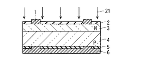
- FIG. 3 is a cross-sectional view showing a light irradiation treatment status with ultraviolet light according to the first embodiment.
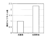
- 5 is a graph showing the effect of the method for manufacturing a solar cell according to Embodiment 1.
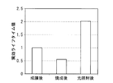
- 5 is a graph showing the effect of the method for manufacturing a solar cell according to Embodiment 2.
- FIG. 1 is a cross-sectional view showing a solar cell structure manufactured by a method for manufacturing a solar cell according to the present embodiment (Embodiment 1 and Embodiment 2).
- a silicon layer 3 having N type conductivity is formed on the surface (the other main surface) of a silicon substrate 4 having P type conductivity (hereinafter referred to as “P type silicon substrate 4”). (Hereinafter referred to as “N-type silicon layer 3”).
- P type silicon substrate 4 P type conductivity
- N-type silicon layer 3 the surface of the P-type silicon substrate 4 is shown as an upper surface and the back surface is a lower surface.
- a surface passivation film 2 having transparency is formed on the surface of the N-type silicon layer 3.
- the surface passivation film 2 for example, a silicon oxide film or a silicon nitride film, an aluminum oxide film, or a laminated film containing them can be considered.
- a surface electrode 1 is selectively formed on the surface of the N-type silicon layer 3 through a part of the surface passivation film 2, so that the surface electrode 1 is electrically connected to the N-type silicon layer 3. Is done.
- a back surface passivation film 5 is formed on the back surface (one main surface) of the P-type silicon substrate 4.
- the back surface passivation film 5 an aluminum oxide film or a laminated film of an aluminum oxide film and a silicon nitride film is employed. Then, a part of the back surface passivation film 5 is penetrated and directly formed on the back surface of the P-type silicon substrate 4, and a back surface electrode 6 is formed on the back surface of the back surface passivation film 5. Therefore, the back electrode 6 is electrically connected to the P-type silicon substrate 4.
- the passivation films 2 and 5 are formed in order to suppress the reduction of the lifetime of the carrier. That is, many defects (such as lattice defects) are generated on the front surface of the N-type silicon layer 3 or the back surface of the P-type silicon substrate 4, and minority carriers generated by light irradiation are recombined through the defects. Therefore, by forming the surface passivation film 2 and the back surface passivation film 5 on the surface of the N-type silicon layer 3 and the back surface of the P-type silicon substrate 4, carrier recombination is suppressed, and as a result, the lifetime of the carrier is reduced. Can be improved.
- the present invention relates to an improvement in film quality of a back surface passivation film 5 formed on the back surface of a P-type silicon substrate 4 in a method for manufacturing a solar cell, and the present invention is hereinafter based on the drawings showing embodiments thereof. This will be specifically described.
- FIG. 2 is an explanatory diagram showing a schematic configuration of a film forming apparatus for realizing the film forming method of the back surface passivation film 5 in the present embodiment (Embodiment 1 and Embodiment 2).
- the film forming apparatus used in the film forming method of the present embodiment includes a reaction vessel 11, a heater 13 for heating the reaction vessel 11, a solution vessel 15 for containing a (material) solution 14, and
- the mist generator 16 is configured to mist the solution 14 in the solution container 15.
- the back surface of the P-type silicon substrate 4 is sprayed on the back surface of the P-type silicon substrate 4 in the reaction vessel 11 through the path L1 with the solution 14 mistified by the mist generator 16.
- a back surface passivation film 5 made of an aluminum oxide film can be formed thereon.
- the P-type silicon substrate 4 is placed on the heater 13 in the reaction vessel 11 in such a manner that the back surface is the top surface and the front surface is the bottom surface.
- mist liquid solution 14 having a small particle size
- a back surface passivation film 5 is formed on the back surface of the P-type silicon substrate 4.
- the heater 13 is a heater or the like, and can heat the P-type silicon substrate 4 placed on the heater 13.
- the heater 13 is heated at the time of film formation by an external control unit (not shown) until reaching a temperature necessary for film formation of the back surface passivation film 5 made of an aluminum oxide film.
- the solution container 15 is filled with a solution 14 serving as a material solution for forming the back surface passivation film 5.
- This solution 14 contains an aluminum (Al) element as a metal source.
- mist generator 16 for example, an ultrasonic atomizer can be employed.
- a mist generator 16 which is an ultrasonic atomizer, mists the solution 14 in the solution container 15 by applying ultrasonic waves to the solution 14 in the solution container 15.
- the misted solution 14 is supplied toward the back surface (upper surface) of the P-type silicon substrate 4 in the reaction vessel 11 through the path L1.
- the solution 14 reacts on the back surface of the P-type silicon substrate 4 under atmospheric pressure which is being heated, and the back surface on the back surface of the P-type silicon substrate 4. A passivation film 5 is formed.
- the solution 14 that has become unreacted in the reaction vessel 11 is always (continuously) discharged out of the reaction vessel 11 through the path L2.
- a P-type silicon substrate 4 having a P-type conductivity is fabricated by introducing predetermined impurities into a silicon substrate whose constituent material is crystalline silicon. Then, the P-type silicon substrate 4 is placed on the heater 13 in the reaction vessel 11. At this time, the P-type silicon substrate 4 is placed on the heater 13 in such a manner that the back surface is the top surface and the front surface is the bottom surface, and the inside of the reaction vessel 11 is set to atmospheric pressure. In this way, the P-type silicon substrate 4 having the back surface and the front surface (one main surface and the other main surface) is manufactured.
- the P-type silicon substrate 4 placed on the heater 13 is heated by the heater 13 until reaching the film formation temperature of the back surface passivation film 5 made of an aluminum oxide film, and the P-type silicon is formed at the film formation temperature. The temperature of the substrate 4 is maintained.
- the solution 14 is misted by the mist generator 16 in the solution container 15.
- the mist solution 14 liquid solution 14 having a small particle diameter
- the solution 14 contains aluminum as a metal source. In this way, the solution 14 (material solution) containing aluminum as a metal element is misted.
- a rectified mist-like solution 14 is supplied to the back surface of the P-type silicon substrate 4 that is heated under atmospheric pressure.
- a back surface passivation film 5 made of an aluminum oxide film is formed on the back surface of the P-type silicon substrate 4.
- the back surface passivation film 5 made of aluminum oxide which is a metal oxide film, is sprayed on the back surface of the P-type silicon substrate 4 under atmospheric pressure (non-vacuum). Is formed on the back surface of the P-type silicon substrate 4.
- the solar cell structure shown in FIG. 1 is manufactured using the P-type silicon substrate 4 on which the back surface passivation film 5 (aluminum oxide film) is formed.
- the back surface passivation film 5 is formed after the surface passivation film 2 and the N-type silicon layer 3 are formed, and then the front surface electrode 1 and the back surface electrode 6 are formed. Note that the order of forming the front surface passivation film 2 and the back surface passivation film 5 may be reversed.
- FIG. 3 is a cross-sectional view showing the state of light irradiation treatment with ultraviolet light 21 according to the first embodiment.
- ultraviolet light 21 predetermined light
- ultraviolet irradiation is performed in which the surface passivation film 2 and the N-type silicon layer 3 are passed from above the surface of the solar cell structure, and the interface between the P-type silicon substrate 4 and the passivation film 5 is irradiated with ultraviolet light 21.
- the solar cell of Embodiment 1 is completed by the light irradiation process using the light 21.
- the film formation method of the back surface passivation film 5 (aluminum oxide film) in the method for manufacturing the solar cell according to Embodiment 1 is the mist method (that is, film formation in which the liquid solution 14 is sprayed under atmospheric pressure). Method), a back surface passivation film 5 is formed on the back surface of the P-type silicon substrate 4.
- the vaporized raw material such as the CVD method or the ALD method is supplied to the P-type silicon substrate 4 to form the back surface passivation film 5 made of the aluminum oxide film.
- the formed liquid solution 14 is sprayed onto the P-type silicon substrate 4 to form the back surface passivation film 5.
- the solution 14 contains an aluminum element. Therefore, the back surface passivation film 5 made of an aluminum oxide film is formed on the back surface of the P-type silicon substrate 4 without using an expensive and difficult material such as TMA (Tri-Methyl-Aluminum). Can be formed.
- TMA Tri-Methyl-Aluminum
- the film forming process is performed under atmospheric pressure, a vacuum process or the like is not necessary, and the manufacturing cost can be reduced.
- the film forming process is performed by spraying the mist-like solution 14 onto the P-type silicon substrate 4. Therefore, in the film forming process, the P-type silicon substrate 4 is not damaged by irradiation with plasma or the like.
- the deposition rate of the back surface passivation film 5 by the mist method is 10 to 15 nm / min, which is 5 times faster than the deposition rate of the aluminum oxide film by the ALD method or the like. Therefore, the production efficiency can be improved by employing the method of forming the back surface passivation film 5 of the first embodiment.
- the light irradiation process of irradiating the ultraviolet light 21 to the interface between the back surface passivation film 5 and the P-type silicon substrate 4 is performed.
- FIG. 4 is a graph showing the effect of the light irradiation process in the first embodiment.
- the lifetime value after film formation of the back surface passivation film 5 (before light irradiation (processing)) is measured, and thereafter light irradiation processing for irradiating ultraviolet light 21 having a wavelength of 365 nm for 30 seconds is performed again.
- the measurement result of measuring the lifetime value is shown.
- FIG. 4 shows an effective lifetime value in which the lifetime value after film formation (before light irradiation) is a normalized value “1”.
- the effective lifetime value increases to about “2.3” after the light irradiation.
- the passivation effect the function of suppressing lifetime reduction of the back surface passivation film 5 manufactured by the method for manufacturing a solar cell in the first embodiment is greatly improved.
- the misted aluminum (material) solution 14 is sprayed on the back surface of the P-type silicon substrate 4 to form a passivation made of an aluminum oxide film.
- the back surface passivation film 5 can be formed with high production efficiency at a low manufacturing cost and without damaging the substrate.
- the passivation film 5 having a good film quality with a significantly improved effective lifetime value can be obtained at the completion stage of the solar cell by the light irradiation treatment with the ultraviolet light 21 performed after the back surface passivation film 5 is formed.
- the film quality of the passivation film 5 can be improved by a light irradiation time of a relatively short time (30 seconds in the example of FIG. 4).
- the firing process at the time of forming the front electrode 1 and the back electrode 6 is generally an indispensable process.
- the baking process is performed.
- Embodiment 1 is a method for manufacturing a solar cell that generally executes the following steps (1) and (2).
- a P-type silicon substrate 4 is produced, and a solution 14 containing aluminum is misted, and the misted solution 14 is sprayed on the back surface of the P-type silicon substrate 4 in a non-vacuum to oxidize.
- a passivation film 5 made of an aluminum film is formed on the back surface of the P-type silicon substrate 4.
- the step of obtaining the solar cell structure shown in FIG. 1 includes the step of forming the surface electrode 1 (the other electrode) and the back electrode 6 (the one electrode) on the front surface side and the back surface side of the P-type silicon substrate 4.
- the step includes a baking process for baking at a predetermined baking temperature.
- the second embodiment is a method for manufacturing a solar cell that performs a light irradiation process in consideration of the influence of the baking process when forming the surface electrode 1 and the back electrode 6 described above, and generally includes the following steps (1), (3), and (2) It is executed via '.
- a P-type silicon substrate 4 is manufactured, and a solution 14 containing aluminum is misted.
- the non-vacuum solution 14 is applied to the back surface of the P-type silicon substrate 4.
- the passivation film 5 made of an aluminum oxide film is formed on the back surface of the P-type silicon substrate 4 by spraying.
- the front electrode 1 and the back electrode 6 are formed to obtain the solar cell structure shown in FIG. At this time, a firing process is performed at a firing temperature of 500 ° C. or higher when the front electrode 1 and the back electrode 6 are formed.
- FIG. 5 is a graph showing the effect of the method for manufacturing the solar cell of the second embodiment.
- the lifetime value after film formation of the back surface passivation film 5 (before light irradiation) is measured, and then a baking process is performed which is a heat treatment at a baking temperature of 800 ° C. and a baking time of 10 seconds under atmospheric pressure.
- the lifetime value after firing (treatment) is measured, and then, as in the first embodiment, a light irradiation treatment of irradiating ultraviolet light 21 having a wavelength of 365 nm for 30 seconds is performed, and the lifetime value is measured.
- FIG. 5 shows an effective lifetime value in which the lifetime value after film formation (before light irradiation) is a normalized value “1”.
- the effective lifetime value increases to about “2.0” after the light irradiation. That is, the effective lifetime value has decreased from “1.0” to “0.5” immediately after the firing process, but the effective lifetime value is set to “1.0” before the firing process by the subsequent light irradiation process. It is improved to "2.0” which greatly exceeds.
- the method for manufacturing the solar cell according to the second embodiment is performed by performing the firing process (step (3)) for forming the front electrode 1 and the back electrode 6 that is substantially indispensable in the manufacturing process of the solar cell.
- the effective lifetime value indicating the quality of the back surface passivation film 5 formed in (1) is temporarily reduced
- the execution of step (2) ′ is performed by performing the light irradiation process in step (2) ′ thereafter. Compared to the previous state, the film quality of the back surface passivation film 5 can be greatly improved.
- the film quality of the back surface passivation film 5 can be improved even in a situation where the baking process is performed at a baking temperature of 800 ° C., which is a baking temperature of 500 ° C. or higher.
- the ultraviolet light 21 is used as the light (predetermined light) used for the light irradiation process
- other types of light may be used.
- light having a photon energy of 1.1 eV or more (wavelength 1100 nm or less) that is, light on the interface between the P-type silicon substrate 4 and the back surface passivation film 5, crystalline silicon in the P-type silicon substrate 4.
- light that can be absorbed by may be used.
- the light used for the light irradiation treatment in the method for manufacturing the solar cell according to the first or second embodiment sunlight or pseudo-sun light having AM1.5 is used, so that the back surface passivation film is relatively inexpensive. 5 film quality can be improved.
Landscapes
- Photovoltaic Devices (AREA)
- Life Sciences & Earth Sciences (AREA)
- Sustainable Development (AREA)
- Chemical & Material Sciences (AREA)
- Crystallography & Structural Chemistry (AREA)
- Engineering & Computer Science (AREA)
- Formation Of Insulating Films (AREA)
- Manufacturing & Machinery (AREA)
- Sustainable Energy (AREA)
Abstract
Description
図1は、本実施の形態(実施の形態1,実施の形態2)である太陽電池の製造方法で製造される太陽電池構造を示す断面図である。
図2は、本実施の形態(実施の形態1,実施の形態2)における裏面パッシベーション膜5の成膜方法を実現するための成膜装置の概略構成を示す説明図である。
次に、実施の形態1の太陽電池の製造方法(特に、裏面パッシベーション膜5(酸化アルミニウム膜)の成膜方法)について説明する。
太陽電池を完成する際、表面電極1及び裏面電極6の形成時における焼成処理は一般的に不可欠な処理となる。例えば、表面電極1及び裏面電極6を形成する際、金属を主成分とする電極材料を塗布した後、焼成処理を実行している。
なお、上述した実施の形態1及び実施の形態2では、光照射処理に用いる光(所定の光)として紫外光21を用いた例を示したが、他の種類の光を用いても良い。例えば、光の光子エネルギーが1.1eV以上(波長1100nm以下)の光、すなわち、P型シリコン基板4及び裏面パッシベーション膜5の界面への光照射を実現すべく、P型シリコン基板4における結晶シリコンが吸収することができる光を、紫外光21の代わりに用いても良い。
5 裏面パッシベーション膜
11 反応容器
13 加熱器
14 (原料)溶液
15 溶液容器
16 ミスト化器
21 紫外光
L1,L2 経路
Claims (9)
- (a) 一方主面及び他方主面を有するシリコン基板(4)を作製するステップと、
(b) 金属元素を含む溶液(14)をミスト化するステップと、
(c) 非真空下で、前記ミスト化された前記溶液を、前記シリコン基板の一方主面に対して噴霧することにより、金属酸化膜からなるパッシベーション膜(5)を前記シリコン基板の一方主面上に成膜するステップと、
(d) 前記パッシベーション膜が形成された前記シリコン基板を用いて太陽電池構造を作製するステップと、
(e) 前記パッシベーション膜と前記シリコン基板との界面に所定の光(21)を照射する光照射処理を行うステップとを備えた、
太陽電池の製造方法。 - 請求項1記載の太陽電池の製造方法であって、
前記金属元素はアルミニウムであり、
前記金属酸化膜は酸化アルミニウムである、
太陽電池の製造方法。 - 請求項1記載の太陽電池の製造方法であって、
前記シリコン基板は、構成材料の結晶シリコンがP型の導電性を有するシリコン基板である、
太陽電池の製造方法。 - 請求項1記載の太陽電池の製造方法であって、
前記ステップ(e)における前記所定の光は、光子エネルギーが1.1eV以上である光を含む、
太陽電池の製造方法。 - 請求項1記載の太陽電池の製造方法であって、
前記ステップ(e)における前記所定の光は、太陽光またはAM1.5を有する疑似太陽の光を含む、
太陽電池の製造方法。 - 請求項4記載の太陽電池の製造方法であって、
前記ステップ(e)における前記所定の光は、365nmの波長を有する紫外光を含む、
太陽電池の製造方法。 - 請求項6記載の太陽電池の製造方法であって、
前記ステップ(e)における、前記紫外光の照射時間は1秒以上である、
太陽電池の製造方法。 - 請求項1~請求項7のうち、いずれか1項に記載の太陽電池の製造方法において、
前記ステップ(d)は、
(d-1) 前記シリコン基板の一方主面側及び他方主面側に一方電極及び他方電極を形成するステップを含み、前記ステップ(d-1)は所定の焼成温度で焼成する焼成処理を含み、
前記ステップ(e)は前記ステップ(d)の後に実行される、
太陽電池の製造方法。 - 請求項8記載の太陽電池の製造方法であって、
前記ステップ (d-1)における前記所定の焼成温度は500℃以上である、
太陽電池の製造方法。
Priority Applications (8)
| Application Number | Priority Date | Filing Date | Title |
|---|---|---|---|
| US15/542,304 US10636919B2 (en) | 2015-03-09 | 2015-03-09 | Solar cell manufacturing method |
| KR1020177019187A KR102153780B1 (ko) | 2015-03-09 | 2015-03-09 | 태양 전지의 제조 방법 |
| KR1020187025763A KR20180101639A (ko) | 2015-03-09 | 2015-03-09 | 태양 전지의 제조 방법 |
| DE112015006280.7T DE112015006280B4 (de) | 2015-03-09 | 2015-03-09 | Herstellungsverfahren einer Solarzelle |
| JP2017504450A JP6360250B2 (ja) | 2015-03-09 | 2015-03-09 | 太陽電池の製造方法 |
| CN201580075408.8A CN107360730B (zh) | 2015-03-09 | 2015-03-09 | 太阳能电池的制造方法 |
| PCT/JP2015/056801 WO2016143025A1 (ja) | 2015-03-09 | 2015-03-09 | 太陽電池の製造方法 |
| TW104136463A TWI607578B (zh) | 2015-03-09 | 2015-11-05 | 太陽電池之製造方法 |
Applications Claiming Priority (1)
| Application Number | Priority Date | Filing Date | Title |
|---|---|---|---|
| PCT/JP2015/056801 WO2016143025A1 (ja) | 2015-03-09 | 2015-03-09 | 太陽電池の製造方法 |
Publications (1)
| Publication Number | Publication Date |
|---|---|
| WO2016143025A1 true WO2016143025A1 (ja) | 2016-09-15 |
Family
ID=56878806
Family Applications (1)
| Application Number | Title | Priority Date | Filing Date |
|---|---|---|---|
| PCT/JP2015/056801 Ceased WO2016143025A1 (ja) | 2015-03-09 | 2015-03-09 | 太陽電池の製造方法 |
Country Status (7)
| Country | Link |
|---|---|
| US (1) | US10636919B2 (ja) |
| JP (1) | JP6360250B2 (ja) |
| KR (2) | KR102153780B1 (ja) |
| CN (1) | CN107360730B (ja) |
| DE (1) | DE112015006280B4 (ja) |
| TW (1) | TWI607578B (ja) |
| WO (1) | WO2016143025A1 (ja) |
Citations (7)
| Publication number | Priority date | Publication date | Assignee | Title |
|---|---|---|---|---|
| JPS63206372A (ja) * | 1987-02-24 | 1988-08-25 | 株式会社豊田中央研究所 | セラミツクス部材の表面改質層形成法 |
| JPH05259156A (ja) * | 1992-03-16 | 1993-10-08 | Fujitsu Ltd | 半導体装置の製造方法 |
| JP2005029408A (ja) * | 2003-07-09 | 2005-02-03 | Nippon Shokubai Co Ltd | 金属酸化物膜の形成方法 |
| JP2006080474A (ja) * | 2004-08-11 | 2006-03-23 | Meidensha Corp | 酸化膜形成方法とその装置 |
| WO2010035313A1 (ja) * | 2008-09-24 | 2010-04-01 | 東芝三菱電機産業システム株式会社 | 金属酸化膜の成膜方法および金属酸化膜の成膜装置 |
| WO2011155635A1 (ja) * | 2010-06-08 | 2011-12-15 | 住友金属鉱山株式会社 | 金属酸化物膜の製造方法及び金属酸化物膜、それを用いた素子、金属酸化物膜付き基板並びにそれを用いたデバイス |
| WO2015004767A1 (ja) * | 2013-07-11 | 2015-01-15 | 東芝三菱電機産業システム株式会社 | 太陽電池の製造方法 |
Family Cites Families (10)
| Publication number | Priority date | Publication date | Assignee | Title |
|---|---|---|---|---|
| JP4481869B2 (ja) * | 2005-04-26 | 2010-06-16 | 信越半導体株式会社 | 太陽電池の製造方法及び太陽電池並びに半導体装置の製造方法 |
| US20080105161A1 (en) * | 2006-11-02 | 2008-05-08 | Tohoku Ricoh Co.,Ltd. | Active energy beam-curable ink for screen printing |
| JP4959733B2 (ja) * | 2008-02-01 | 2012-06-27 | 東京エレクトロン株式会社 | 薄膜形成方法、薄膜形成装置及びプログラム |
| CN101383382A (zh) * | 2008-10-09 | 2009-03-11 | 中国科学院电工研究所 | 一种用于晶硅太阳电池的复合钝化减反膜及其制备方法 |
| TWI518736B (zh) * | 2010-03-31 | 2016-01-21 | Ats自動模具系統股份有限公司 | 光產生系統及其方法 |
| WO2012161135A1 (ja) * | 2011-05-26 | 2012-11-29 | 日立化成工業株式会社 | 半導体基板用パッシベーション膜形成用材料、半導体基板用パッシベーション膜及びその製造方法、並びに太陽電池素子及びその製造方法 |
| KR20130064659A (ko) * | 2011-12-08 | 2013-06-18 | 제일모직주식회사 | 태양전지 전극용 페이스트 조성물 및 이로부터 제조된 전극 |
| KR20130078667A (ko) * | 2011-12-30 | 2013-07-10 | 금오공과대학교 산학협력단 | 실리콘 태양전지의 전면전극 형성용 무기첨가제 및 이를 이용하여 제조된 실리콘 태양전지 |
| GB201209694D0 (en) * | 2012-05-31 | 2012-07-18 | Dow Corning | Passivation of silicon dielectric interface |
| CN102945894A (zh) * | 2012-12-03 | 2013-02-27 | 天威新能源控股有限公司 | 一种晶体硅太阳能电池氧化铝钝化膜和背电极的制备方法 |
-
2015
- 2015-03-09 US US15/542,304 patent/US10636919B2/en active Active
- 2015-03-09 KR KR1020177019187A patent/KR102153780B1/ko active Active
- 2015-03-09 CN CN201580075408.8A patent/CN107360730B/zh active Active
- 2015-03-09 DE DE112015006280.7T patent/DE112015006280B4/de active Active
- 2015-03-09 JP JP2017504450A patent/JP6360250B2/ja active Active
- 2015-03-09 WO PCT/JP2015/056801 patent/WO2016143025A1/ja not_active Ceased
- 2015-03-09 KR KR1020187025763A patent/KR20180101639A/ko not_active Withdrawn
- 2015-11-05 TW TW104136463A patent/TWI607578B/zh active
Patent Citations (7)
| Publication number | Priority date | Publication date | Assignee | Title |
|---|---|---|---|---|
| JPS63206372A (ja) * | 1987-02-24 | 1988-08-25 | 株式会社豊田中央研究所 | セラミツクス部材の表面改質層形成法 |
| JPH05259156A (ja) * | 1992-03-16 | 1993-10-08 | Fujitsu Ltd | 半導体装置の製造方法 |
| JP2005029408A (ja) * | 2003-07-09 | 2005-02-03 | Nippon Shokubai Co Ltd | 金属酸化物膜の形成方法 |
| JP2006080474A (ja) * | 2004-08-11 | 2006-03-23 | Meidensha Corp | 酸化膜形成方法とその装置 |
| WO2010035313A1 (ja) * | 2008-09-24 | 2010-04-01 | 東芝三菱電機産業システム株式会社 | 金属酸化膜の成膜方法および金属酸化膜の成膜装置 |
| WO2011155635A1 (ja) * | 2010-06-08 | 2011-12-15 | 住友金属鉱山株式会社 | 金属酸化物膜の製造方法及び金属酸化物膜、それを用いた素子、金属酸化物膜付き基板並びにそれを用いたデバイス |
| WO2015004767A1 (ja) * | 2013-07-11 | 2015-01-15 | 東芝三菱電機産業システム株式会社 | 太陽電池の製造方法 |
Also Published As
| Publication number | Publication date |
|---|---|
| CN107360730B (zh) | 2020-03-24 |
| DE112015006280T5 (de) | 2018-01-18 |
| JP6360250B2 (ja) | 2018-07-18 |
| JPWO2016143025A1 (ja) | 2017-08-31 |
| US20180269340A1 (en) | 2018-09-20 |
| KR102153780B1 (ko) | 2020-09-08 |
| TWI607578B (zh) | 2017-12-01 |
| CN107360730A (zh) | 2017-11-17 |
| US10636919B2 (en) | 2020-04-28 |
| TW201633557A (zh) | 2016-09-16 |
| KR20180101639A (ko) | 2018-09-12 |
| KR20170094373A (ko) | 2017-08-17 |
| DE112015006280B4 (de) | 2024-12-24 |
Similar Documents
| Publication | Publication Date | Title |
|---|---|---|
| CN106463548B (zh) | 太阳能电池元件以及太阳能电池模块 | |
| CN117766623B (zh) | 一种太阳电池的制备方法、太阳电池及光伏组件 | |
| CN105355671B (zh) | 一种宽光谱高效太阳能光伏电池 | |
| TW201515244A (zh) | 太陽電池及太陽電池模組 | |
| JP6688244B2 (ja) | 高効率太陽電池の製造方法及び太陽電池セルの製造システム | |
| JP6109939B2 (ja) | 太陽電池の製造方法 | |
| JP6360250B2 (ja) | 太陽電池の製造方法 | |
| CN103746006A (zh) | 一种晶体硅太阳能电池的钝化层及其钝化工艺 | |
| CN108281496A (zh) | 一种硅基PiN紫外光电二极管及其制备方法 | |
| CN203910818U (zh) | 背钝化层结构及背钝化p型太阳能电池 | |
| JP2014212219A (ja) | 太陽電池及びその製造方法 | |
| HK1240398A1 (en) | Solar cell manufacturing method | |
| HK1240398B (zh) | 太阳能电池的制造方法 | |
| JP2006344883A (ja) | 太陽電池の製造方法 | |
| US20190386158A1 (en) | Plasma-curing of light-receiving surfaces of solar cells | |
| TWI614906B (zh) | 半導體裝置及其製造方法 | |
| TWI382558B (zh) | 太陽能電池面板的製作方法 | |
| JP2013149820A (ja) | 太陽電池の製造方法及び太陽電池 | |
| KR20120131643A (ko) | 고효율 태양전지 제조방법 | |
| Hsieh et al. | Plasmonic optical enhancement of solar module | |
| JP2011187858A (ja) | 太陽電池の製造方法及び太陽電池 | |
| WO2019193181A1 (en) | Method for manufacturing a photovoltaic device | |
| CN107394003A (zh) | 制造太阳能电池的方法 | |
| CN103746007A (zh) | 一种p型晶体硅太阳能电池的钝化层及其钝化工艺 | |
| TW201547049A (zh) | 太陽能電池背電極鈍化層的製造方法 |
Legal Events
| Date | Code | Title | Description |
|---|---|---|---|
| 121 | Ep: the epo has been informed by wipo that ep was designated in this application |
Ref document number: 15884521 Country of ref document: EP Kind code of ref document: A1 |
|
| ENP | Entry into the national phase |
Ref document number: 2017504450 Country of ref document: JP Kind code of ref document: A |
|
| WWE | Wipo information: entry into national phase |
Ref document number: 15542304 Country of ref document: US |
|
| ENP | Entry into the national phase |
Ref document number: 20177019187 Country of ref document: KR Kind code of ref document: A |
|
| WWE | Wipo information: entry into national phase |
Ref document number: 112015006280 Country of ref document: DE |
|
| 122 | Ep: pct application non-entry in european phase |
Ref document number: 15884521 Country of ref document: EP Kind code of ref document: A1 |