WO2016129410A1 - 撮像素子、駆動方法、および電子機器 - Google Patents
撮像素子、駆動方法、および電子機器 Download PDFInfo
- Publication number
- WO2016129410A1 WO2016129410A1 PCT/JP2016/052592 JP2016052592W WO2016129410A1 WO 2016129410 A1 WO2016129410 A1 WO 2016129410A1 JP 2016052592 W JP2016052592 W JP 2016052592W WO 2016129410 A1 WO2016129410 A1 WO 2016129410A1
- Authority
- WO
- WIPO (PCT)
- Prior art keywords
- charge
- charge storage
- pixel
- photoelectric conversion
- conversion unit
- Prior art date
- Legal status (The legal status is an assumption and is not a legal conclusion. Google has not performed a legal analysis and makes no representation as to the accuracy of the status listed.)
- Ceased
Links
Images







Classifications
-
- H—ELECTRICITY
- H04—ELECTRIC COMMUNICATION TECHNIQUE
- H04N—PICTORIAL COMMUNICATION, e.g. TELEVISION
- H04N25/00—Circuitry of solid-state image sensors [SSIS]; Control thereof
- H04N25/50—Control of the SSIS exposure
- H04N25/57—Control of the dynamic range
- H04N25/59—Control of the dynamic range by controlling the amount of charge storable in the pixel, e.g. modification of the charge conversion ratio of the floating node capacitance
-
- H—ELECTRICITY
- H04—ELECTRIC COMMUNICATION TECHNIQUE
- H04N—PICTORIAL COMMUNICATION, e.g. TELEVISION
- H04N25/00—Circuitry of solid-state image sensors [SSIS]; Control thereof
- H04N25/50—Control of the SSIS exposure
- H04N25/57—Control of the dynamic range
- H04N25/58—Control of the dynamic range involving two or more exposures
- H04N25/581—Control of the dynamic range involving two or more exposures acquired simultaneously
- H04N25/583—Control of the dynamic range involving two or more exposures acquired simultaneously with different integration times
-
- H—ELECTRICITY
- H04—ELECTRIC COMMUNICATION TECHNIQUE
- H04N—PICTORIAL COMMUNICATION, e.g. TELEVISION
- H04N25/00—Circuitry of solid-state image sensors [SSIS]; Control thereof
- H04N25/50—Control of the SSIS exposure
- H04N25/57—Control of the dynamic range
- H04N25/58—Control of the dynamic range involving two or more exposures
- H04N25/581—Control of the dynamic range involving two or more exposures acquired simultaneously
- H04N25/585—Control of the dynamic range involving two or more exposures acquired simultaneously with pixels having different sensitivities within the sensor, e.g. fast or slow pixels or pixels having different sizes
-
- H—ELECTRICITY
- H04—ELECTRIC COMMUNICATION TECHNIQUE
- H04N—PICTORIAL COMMUNICATION, e.g. TELEVISION
- H04N25/00—Circuitry of solid-state image sensors [SSIS]; Control thereof
- H04N25/60—Noise processing, e.g. detecting, correcting, reducing or removing noise
- H04N25/62—Detection or reduction of noise due to excess charges produced by the exposure, e.g. smear, blooming, ghost image, crosstalk or leakage between pixels
- H04N25/621—Detection or reduction of noise due to excess charges produced by the exposure, e.g. smear, blooming, ghost image, crosstalk or leakage between pixels for the control of blooming
- H04N25/622—Detection or reduction of noise due to excess charges produced by the exposure, e.g. smear, blooming, ghost image, crosstalk or leakage between pixels for the control of blooming by controlling anti-blooming drains
-
- H—ELECTRICITY
- H04—ELECTRIC COMMUNICATION TECHNIQUE
- H04N—PICTORIAL COMMUNICATION, e.g. TELEVISION
- H04N25/00—Circuitry of solid-state image sensors [SSIS]; Control thereof
- H04N25/70—SSIS architectures; Circuits associated therewith
- H04N25/76—Addressed sensors, e.g. MOS or CMOS sensors
- H04N25/77—Pixel circuitry, e.g. memories, A/D converters, pixel amplifiers, shared circuits or shared components
-
- H—ELECTRICITY
- H04—ELECTRIC COMMUNICATION TECHNIQUE
- H04N—PICTORIAL COMMUNICATION, e.g. TELEVISION
- H04N25/00—Circuitry of solid-state image sensors [SSIS]; Control thereof
- H04N25/70—SSIS architectures; Circuits associated therewith
- H04N25/76—Addressed sensors, e.g. MOS or CMOS sensors
- H04N25/77—Pixel circuitry, e.g. memories, A/D converters, pixel amplifiers, shared circuits or shared components
- H04N25/771—Pixel circuitry, e.g. memories, A/D converters, pixel amplifiers, shared circuits or shared components comprising storage means other than floating diffusion
-
- H—ELECTRICITY
- H04—ELECTRIC COMMUNICATION TECHNIQUE
- H04N—PICTORIAL COMMUNICATION, e.g. TELEVISION
- H04N25/00—Circuitry of solid-state image sensors [SSIS]; Control thereof
- H04N25/70—SSIS architectures; Circuits associated therewith
- H04N25/76—Addressed sensors, e.g. MOS or CMOS sensors
- H04N25/78—Readout circuits for addressed sensors, e.g. output amplifiers or A/D converters
-
- H—ELECTRICITY
- H10—SEMICONDUCTOR DEVICES; ELECTRIC SOLID-STATE DEVICES NOT OTHERWISE PROVIDED FOR
- H10F—INORGANIC SEMICONDUCTOR DEVICES SENSITIVE TO INFRARED RADIATION, LIGHT, ELECTROMAGNETIC RADIATION OF SHORTER WAVELENGTH OR CORPUSCULAR RADIATION
- H10F39/00—Integrated devices, or assemblies of multiple devices, comprising at least one element covered by group H10F30/00, e.g. radiation detectors comprising photodiode arrays
- H10F39/80—Constructional details of image sensors
- H10F39/802—Geometry or disposition of elements in pixels, e.g. address-lines or gate electrodes
- H10F39/8023—Disposition of the elements in pixels, e.g. smaller elements in the centre of the imager compared to larger elements at the periphery
-
- H—ELECTRICITY
- H10—SEMICONDUCTOR DEVICES; ELECTRIC SOLID-STATE DEVICES NOT OTHERWISE PROVIDED FOR
- H10F—INORGANIC SEMICONDUCTOR DEVICES SENSITIVE TO INFRARED RADIATION, LIGHT, ELECTROMAGNETIC RADIATION OF SHORTER WAVELENGTH OR CORPUSCULAR RADIATION
- H10F39/00—Integrated devices, or assemblies of multiple devices, comprising at least one element covered by group H10F30/00, e.g. radiation detectors comprising photodiode arrays
- H10F39/80—Constructional details of image sensors
- H10F39/803—Pixels having integrated switching, control, storage or amplification elements
- H10F39/8037—Pixels having integrated switching, control, storage or amplification elements the integrated elements comprising a transistor
-
- H—ELECTRICITY
- H10—SEMICONDUCTOR DEVICES; ELECTRIC SOLID-STATE DEVICES NOT OTHERWISE PROVIDED FOR
- H10F—INORGANIC SEMICONDUCTOR DEVICES SENSITIVE TO INFRARED RADIATION, LIGHT, ELECTROMAGNETIC RADIATION OF SHORTER WAVELENGTH OR CORPUSCULAR RADIATION
- H10F39/00—Integrated devices, or assemblies of multiple devices, comprising at least one element covered by group H10F30/00, e.g. radiation detectors comprising photodiode arrays
- H10F39/10—Integrated devices
- H10F39/12—Image sensors
- H10F39/18—Complementary metal-oxide-semiconductor [CMOS] image sensors; Photodiode array image sensors
- H10F39/186—Complementary metal-oxide-semiconductor [CMOS] image sensors; Photodiode array image sensors having arrangements for blooming suppression
- H10F39/1865—Overflow drain structures
-
- H—ELECTRICITY
- H10—SEMICONDUCTOR DEVICES; ELECTRIC SOLID-STATE DEVICES NOT OTHERWISE PROVIDED FOR
- H10F—INORGANIC SEMICONDUCTOR DEVICES SENSITIVE TO INFRARED RADIATION, LIGHT, ELECTROMAGNETIC RADIATION OF SHORTER WAVELENGTH OR CORPUSCULAR RADIATION
- H10F39/00—Integrated devices, or assemblies of multiple devices, comprising at least one element covered by group H10F30/00, e.g. radiation detectors comprising photodiode arrays
- H10F39/80—Constructional details of image sensors
- H10F39/805—Coatings
- H10F39/8057—Optical shielding
Definitions
- the present disclosure relates to an imaging device, a driving method, and an electronic device, and more particularly, to an imaging device, a driving method, and an electronic device that can capture an image with a higher dynamic range.
- a solid-state imaging device such as a CCD (Charge Coupled Device) or a CMOS (Complementary Metal Oxide Semiconductor) image sensor is used.
- a solid-state imaging device has a pixel in which a PD (photodiode) that performs photoelectric conversion and a plurality of transistors are combined, and is based on pixel signals output from a plurality of pixels arranged in a plane. An image is constructed.
- the pixel signals output from the pixels are AD-converted in parallel by a plurality of AD (Analog to Digital) converters arranged for each column of pixels, for example, and output.
- AD Analog to Digital
- Patent Document 1 in a pixel having first and second charge storage units, charges equal to or less than the saturation charge amount of the first charge storage unit are stored in the first charge storage unit, and the first charge is stored.
- a solid-state imaging device that is driven so that charges exceeding the saturation charge amount of the storage unit are stored in the first and second charge storage units.
- the HDR ratio can be expanded while improving the SNR (signal-to-noise ratio) by performing three-stage HDR synthesis of low illuminance, medium illuminance, and large illuminance.
- the present disclosure has been made in view of such a situation, and makes it possible to capture an image with a higher dynamic range.
- An imaging device includes a photoelectric conversion unit that converts incident light into electric charge by photoelectric conversion and stores the charge, and two or more charge storage units that store charge transferred from the photoelectric conversion unit.
- the pixel region in which a plurality of pixels are arranged, and the transfer of charges having different exposure times from the photoelectric conversion unit to two or more charge storage units so as to be repeated during a light receiving period of one frame.
- a driving unit for driving the motor.
- a driving method includes a photoelectric conversion unit that converts incident light into charges by photoelectric conversion and stores the charge, and two or more charge storage units that store charges transferred from the photoelectric conversion unit.
- the driving unit supplies charges having different exposure times to two or more charge storage units. The transfer from the photoelectric conversion unit is repeated during the light receiving period of one frame.
- An electronic device includes a photoelectric conversion unit that converts incident light into electric charge by photoelectric conversion and stores the charge, and two or more charge storage units that store charge transferred from the photoelectric conversion unit.
- the pixel region in which a plurality of pixels are arranged, and the transfer of charges having different exposure times from the photoelectric conversion unit to two or more charge storage units so as to be repeated during a light receiving period of one frame.
- an image sensor having a drive unit for driving the image sensor.
- the transfer of charges having different exposure times from the photoelectric conversion unit to two or more charge storage units is repeated during a light receiving period of one frame.
- FIG. 1 is a block diagram illustrating a configuration example of an embodiment of an image sensor to which the present technology is applied.
- the image sensor 1 includes a pixel region 2, a vertical drive circuit 3, a column signal processing circuit 4, a horizontal drive circuit 5, an output circuit 6, and a control circuit 7.
- the pixel region 2 is a light receiving surface that receives light collected by an optical system (not shown).
- a plurality of pixels 11 are arranged in a matrix, and each pixel 11 is connected to the vertical drive circuit 3 for each row via a horizontal signal line and via a vertical signal line.
- Each column is connected to a column signal processing circuit 4.
- the plurality of pixels 11 each output a pixel signal at a level corresponding to the amount of light received, and an image of the subject imaged in the pixel region 2 is constructed from these pixel signals.
- the vertical drive circuit 3 sequentially supplies a drive signal for driving (transferring, selecting, resetting, etc.) each pixel 11 for each row of the plurality of pixels 11 arranged in the pixel region 2 via a horizontal signal line. To the pixel 11.
- the column signal processing circuit 4 performs AD conversion of the pixel signal by performing CDS (Correlated Double Sampling) processing on the pixel signal output from the plurality of pixels 11 through the vertical signal line. At the same time, reset noise is removed.
- CDS Correlated Double Sampling
- the horizontal drive circuit 5 sequentially outputs a drive signal for outputting a pixel signal from the column signal processing circuit 4 to the data output signal line for each column of the plurality of pixels 11 arranged in the pixel region 2. To supply.
- the output circuit 6 amplifies the pixel signal supplied from the column signal processing circuit 4 via the data output signal line at a timing according to the driving signal of the horizontal driving circuit 5 and outputs the amplified pixel signal to the subsequent signal processing circuit.
- the control circuit 7 controls driving of each block inside the image sensor 1. For example, the control circuit 7 generates a clock signal according to the drive cycle of each block and supplies it to each block.
- the pixel 11 is configured to include a plurality of charge storage units so that a moving image of an HDR image can be captured. Accumulated in.
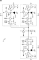
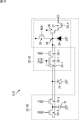
- FIG. 2 shows a circuit diagram of a first configuration example of the pixel 11.
- the pixel 11 includes a PD 21, charge readout paths 22-1 to 22-3, and an anti-blooming gate 23.
- the PD 21 is a photoelectric conversion unit that converts incident light into electric charge by photoelectric conversion and accumulates it.
- the PD 21 has an anode terminal grounded, a cathode terminal connected to a vertical signal line via each of the charge readout paths 22-1 to 22-3, and a drain connected via an anti-blooming gate 23. Yes.
- the charge read path 22-1 includes a transfer gate 31-1, a charge storage gate 32-1, a read gate 33-1, an FD unit 34-1, a storage capacitor 35-1, an amplification transistor 36-1, and a selection transistor 37-1. And a reset transistor 38-1.
- the charge readout paths 22-2 and 22-3 are configured in the same manner as the charge readout path 22-1 and will not be described in detail.
- the gate electrode of the transfer gate 31-1 is connected to the gate electrode of the charge storage gate 32-1, and the transfer gate 31-1 and the charge storage gate 32-1 are connected to the transfer pulse FSG1 / STG1 applied to the gate electrode. And is driven at the same timing. That is, at the timing when the transfer pulse FSG1 / STG1 is turned on, the charge accumulated in the PD 21 is transferred to the charge accumulation gate 32-1 via the transfer gate 31-1, and accumulated in the charge accumulation gate 32-1.
- the read gate 33-1 is driven according to the read pulse ROG1 applied to the gate electrode, and the charge stored in the charge storage gate 32-1 is read to the FD unit 34-1 at the timing when the read pulse ROG1 is turned on. It is.
- the FD unit 34-1 is a floating diffusion region having a predetermined storage capacitor 35-1 connected to the gate electrode of the amplification transistor 36-1, and charges transferred through the read gate 33-1 are stored in the storage capacitor 35-1. Temporarily store in -1.
- the amplifying transistor 36-1 outputs a pixel signal of a level corresponding to the charge accumulated in the storage capacitor 35-1 of the FD unit 34-1 (that is, the potential of the FD unit 34-1) to the selection transistor 37-1.
- the FD unit 34-1 allows the charge transferred from the PD 21 to the charge storage gate 32-1 according to the charge. It functions as a charge-voltage converter for converting into a level pixel signal.
- the selection transistor 37-1 is driven according to the selection signal SEL1 supplied from the vertical drive circuit 3.
- the selection transistor 37-1 is turned on, the pixel signal output from the amplification transistor 36-1 can be output to the vertical signal line. It becomes a state.
- the reset transistor 38-1 is driven in accordance with the reset signal RG1 supplied from the vertical drive circuit 3.
- the reset transistor 38-1 is turned on, the charge stored in the storage capacitor 35-1 of the FD unit 34-1 is changed. It is discharged to the drain. As a result, the storage capacitor 35-1 of the FD unit 34-1 is reset.
- the charge readout path 22-1 is configured, and the pixel signal corresponding to the charge transferred from the PD 21 to the charge accumulation gate 32-1 is read out through the charge readout path 22-1.
- the pixel signal corresponding to the charge transferred from the PD 21 to the charge storage gate 32-2 is read out in the charge reading path 22-2, and the charge storage gate 32-3 from the PD 21 in the charge reading path 22-3.
- a pixel signal corresponding to the charge transferred to is read out.
- the anti-blooming gate 23 is driven according to the discharge pulse ABG applied to the gate electrode, and the shutter control is performed by discharging the charge accumulated in the PD 21 to the drain at the timing when the discharge pulse ABG is turned on. .
- the potential of the anti-blooming gate 23 is set so that charges overflow from the PD 21 through the anti-blooming gate 23 when very strong light is incident on the PD 21.
- the pixel 11 configured as described above can read out the electric charge generated in the PD 21 through the electric charge reading paths 22-1 to 22-3 in accordance with the driving of the vertical driving circuit 3 in FIG. Accordingly, the pixel 11 sequentially transfers the charge of the PD 21 to the charge accumulation gate 32-1, the charge accumulation gate 32-2, and the charge accumulation gate 32-3 during one frame of light receiving period, and each has three different exposure times. Charge (pixel signal) can be accumulated. And with such a driving method, the image sensor 1 can acquire pixel signals having different exposure times.
- the imaging device 1 transfers a charge having a short accumulation time (hereinafter referred to as short accumulation) to the charge accumulation gate 32-1, and a charge having a medium accumulation time (hereinafter referred to as medium accumulation). Is transferred to the charge storage gate 32-2, and the pixel 11 is driven by a driving method in which a charge having a long storage time (hereinafter referred to as long storage) is transferred to the charge storage gate 32-3.
- the timing for supplying the transfer pulse FSG / STG for transferring charges is set to a period sufficiently shorter than one frame, and the charge accumulation gate 32-1, the charge accumulation gate 32-2, and the charge accumulation gate 32- 3 is performed (hereinafter referred to as “burst distribution driving” as appropriate).
- the image sensor 1 then reads out the pixel signals corresponding to the charges transferred to the charge storage gate 32-1, the charge storage gate 32-2, and the charge storage gate 32-3 after one frame of storage, and performs HDR synthesis. Done. Thereby, an HDR image having a sufficiently wide dynamic range can be acquired.
- the exposure ratio of charges transferred to the charge storage gate 32-1, the charge storage gate 32-2, and the charge storage gate 32-3 is set to 1 (60dB): 32 (+ 30dB): 1000 (+ 30dB).
- the image sensor 1 can acquire an HDR image of 120 dB.
- the saturation charge amount of the PD 21 and the charge storage gate 32 is mainly 10,000 electrons or less.
- HDR synthesis is performed from images having a plurality of sensitivity differences, if an image with high illuminance is to be synthesized from a noise level of several electrons, it is synthesized with a high SNR image having a low saturation signal on the low illuminance side.
- the SNR difference becomes too wide at the part, causing image corruption.
- a signal on the high illuminance side cannot be used for HDR synthesis unless it is a signal having a certain SNR or more.
- the visually acceptable level is about 20 dB
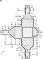
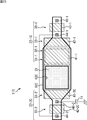
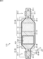
- FIG. 3 shows a planar configuration example of the pixel 11 shown in FIG.
- charge readout paths 22-1 to 22-3 are formed so as to be connected to the three sides of the PD 21 formed in a substantially square shape, and the pixel 11 is connected to the remaining one side.
- a blooming gate 23 is formed.
- a transfer gate 31-1, a charge storage gate 32-1, a readout gate 33-1 and a reset transistor 38-1 are arranged in this order from the PD 21 side.
- the charge readout paths 22-2 and 22-3 are configured in the same manner as the charge readout path 22-1 and will not be described in detail.
- the amplification transistor 36 and the selection transistor 37 are not shown.
- the transfer gate 31-1 and the charge storage gate 32-1 are configured to have a common gate electrode 41-1, and the gate electrode 41-1 is disposed adjacent to the PD 21.
- a through electrode 44-1 connected to the FD portion 34 is disposed between the gate electrode 42-1 constituting the read gate 33-1 and the gate electrode 43-1 constituting the reset transistor 38-1.
- a through electrode 45-1 connected to the drain of the reset transistor 38-1 is arranged on the opposite side of the through electrode 44-1 with respect to the gate electrode 43-1.
- a gate electrode 51-1 is disposed adjacent to the PD 21, and a through electrode 52 connected to the drain is disposed on the opposite side of the PD 21 with respect to the gate electrode 51-1.
- a light shielding film 61 is formed on the light receiving surface side of the pixel 11 so as to shield the charge readout paths 22-1 to 22-3 and the anti-blooming gate 23.
- the light shielding film 61 transmits light to the PD 21. Is formed.
- the pixel 11 is configured such that the charge readout paths 22-1 to 22-3 are arranged in three directions (3 tap structure) and the anti-blooming gate 23 is arranged in the remaining one direction. With such a configuration, as described above, the pixel 11 can read out charges having different exposure times through the charge reading paths 22-1 to 22-3.
- the pixel 11 includes charge storage gates 32-1 to 32-3 having a buried channel type structure with a gate electrode as a charge storage portion for storing the charges transferred from the PD 21.
- the pixel 11 can employ charge storage portions having various structures such as a floating diffusion type and a buried channel type with a virtual gate. In this case, the capacities of those charge storage units can be set according to the dynamic range ratio and SNR.
- the pixel 11 may have a structure without the anti-blooming gate 23 because the dynamic range can be increased. Furthermore, it is possible to adopt an FD sharing structure that has been widely used in recent years for miniaturization, and it is possible to share circuits after the FD section 34.
- the FD unit 34-1, the FD unit 34-2, and the FD unit 34-3 are connected to each other, and the reset transistor 38, the amplification transistor 36, and the selection transistor 37 that are provided one by one are connected to the charge readout path.
- a structure shared by 22-1 to 22-3 can be adopted.
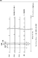
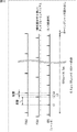
- the exposure time per frame is 16.7 ms. Then, after the image pickup for one frame is completed, the image pickup device 1 sequentially performs rolling shutter reading for each row.
- charges are transferred from the PD 21 in the order of long accumulation transfer to the charge accumulation gate 32-3, short accumulation transfer to the charge accumulation gate 32-1, and intermediate accumulation transfer to the charge accumulation gate 32-2. Is done.
- the charge exposure time per transfer of charges that is performed a plurality of times for the charge storage gate 32-3, the charge storage gate 32-1, and the charge storage gate 32-2 is 1 It is set to be sufficiently shorter than the frame, and transfer of long accumulation, short accumulation, and intermediate accumulation is repeatedly performed in one frame.
- the exposure time of long accumulation, short accumulation, and intermediate accumulation transferred to the charge accumulation gate 32-3, the charge accumulation gate 32-1, and the charge accumulation gate 32-2, respectively, is the charge accumulation gate 32-3.
- the charge storage gate 32-1 and the charge storage gate 32-2 are substantially the same.
- the discharge pulse ABG is turned on, and the long accumulation exposure is started from the timing when the charge accumulated in the PD 21 is discharged through the anti-blooming gate 23.
- the transfer pulse FSG3 is turned on, and the long accumulation is transferred from the PD 21 to the charge accumulation gate 32-3 and accumulated.
- the discharge pulse ABG is turned on to start exposure for short accumulation.
- the transfer pulse FSG1 is turned on, and short accumulation is transferred from the PD 21 to the charge accumulation gate 32-1 and accumulated.
- the discharge pulse ABG is turned on to start the intermediate storage exposure.
- the transfer pulse FSG2 is turned on, and the intermediate storage is transferred from the PD 21 to the charge storage gate 32-2, and stored. Is done.
- FIG. 4 shows an example in which imaging is performed with a sensitivity of 1/2 with respect to the maximum sensitivity of the pixel 11.
- the long accumulation exposure time (time from time t1 to time t2) is a period from the timing when the transfer pulse FSG2 is turned on immediately before time t1 to the timing when the transfer pulse FSG3 is turned on at time t2. Is determined by setting time t1 to.
- the long accumulation exposure time is set to the maximum (maximum sensitivity)
- the long accumulation exposure may be started by setting time t1 at the same time as the transfer pulse FSG2 is turned on immediately before, as shown in FIG.
- time t1 is set at a timing at which the period becomes 1/2.
- all the discharge driving of the discharge pulse ABG may be turned off.
- the short accumulation exposure time (time from time t3 to time t4) is set to time t3 at a timing at which the period from time t2 to time t4 is halved.
- the exposure time (time from time t5 to time t6) of the intermediate storage is set to time t5 at a timing at which the period from time t4 to time t6 is halved.
- the synchronous circuit design can be facilitated by setting the transfer pulses FSG1 to FSG3 and the discharge pulse ABG to be synchronized with one line of the rolling shutter readout.
- the image sensor 1 can generate three images with different exposure times and perform HDR synthesis only by controlling the timing of transferring charges in the pixels 11. At this time, for example, the imaging device 1 can perform the synthesis even when the short-charged charge is small, and can improve the SNR at the stage of performing the HDR synthesis. Thereby, the image sensor 1 can acquire an HDR image with less noise.
- the imaging device 1 is configured to include two or more charge accumulation gates 32-1 to 32-3 in the configuration example of FIG. 2 for one PD 21, and performs burst distribution driving. By doing so, the exposure time ratio of the HDR image is controlled. Thus, by distributing the transfer of charges to the charge accumulation gates 32-1 to 32-3 in a time-sharing manner, the image sensor 1 can reliably capture an image with a high dynamic range.
- the imaging device 1 Since the imaging device 1 has a structure using one PD 21, sensitivity loss can be suppressed, SNR at low illuminance can be improved, and a high dynamic range can be achieved at the same time. An image can be taken.
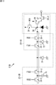
- FIG. 5 shows a circuit diagram of the pixel 11A as the second configuration example
- FIG. 6 shows a planar configuration example of the pixel 11A.
- the pixel 11A includes a PD 21, charge readout paths 22-1A and 22-2A, and an anti-blooming gate 23.
- the PD 21, the charge readout path 22-1A, and the anti-blooming gate 23 are configured in the same manner as the pixel 11 in FIG. 2, and a detailed description thereof is omitted.
- the pixel 11 in FIG. 2 includes three charge readout paths 22-1 to 22-3, whereas the pixel 11A includes two charge readout paths 22-1A and 22-2A.
- the configuration of the path 22-2A is different from that of the pixel 11 in FIG.
- the charge readout path 22-2A includes a transfer gate 31-2, a capacitor 71, a readout gate 33-2, an FD unit 34-2, a storage capacitor 35-2, an amplification transistor 36-2, a selection transistor 37-2, and a reset transistor. 38-2.
- the charge readout path 22-2A is connected via the through electrode 46-2 via the diffusion junction instead of the charge accumulation gate 32-2 as compared with the charge readout path 22-2 of FIG. It is different in that it is provided with a capacitor 71 to be configured.
- the charge of the PD 21 is transferred to the capacitor 71 via the transfer gate 31-2 and stored. That is, the pixel 11A employs a capacitor-type charge storage unit instead of a buried channel-type charge storage unit as a charge storage unit in the charge readout path 22-2A.
- the pixel 11A can make the storage capacity of the capacitor 71 in the charge readout path 22-2A larger than the charge storage gate 32-2 in the charge readout path 22-2 in FIG. Therefore, in the pixel 11A, by transferring the long accumulation to the charge accumulation gate 32-1, it is possible to realize a high SNR from a low illuminance. Furthermore, in the pixel 11A, by transferring the short accumulation to the capacitor 71, it is possible to prevent the electric charge from overflowing even for a high-luminance subject such as the sun. That is, the pixel 11A is designed such that the capacitor 71 and the charge storage gate 32-2 have different charge storage capacities, and the long storage is transferred to the charge storage gate 32-2, which has a small charge storage capacity. The short accumulation is transferred to the capacitor 71 having a large capacity.
- the difference between the storage times is set to 1: 1000 (+ 60dB).
- the imaging device 1 including such a pixel 11A captures an HDR image having a sufficient dynamic range even if the imaging device 1 includes two charge readout paths 22-1A and 22-2A (2tap structure). Can do. Furthermore, the pixel 11A has a simple configuration as compared with the pixel 11, and the imaging element 1 including the pixel 11A has a structure advantageous for miniaturization, for example.
- a charge storage unit having various structures such as a floating diffusion type and a buried channel type with a virtual gate can be adopted.
- the capacities of those charge storage units can be set to different capacities depending on the dynamic range ratio and SNR.
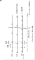
- charges are transferred from the PD 21 in the order of long accumulation transfer to the charge accumulation gate 32-1 and short accumulation transfer to the capacitor 71. Then, the charge exposure time per charge transfer performed a plurality of times on the charge storage gate 32-1 and the capacitor 71 is set to be sufficiently shorter than one frame, so that long storage and short storage transfer can be performed. Repeatedly in one frame.
- the discharge pulse ABG is turned on, and the long accumulation exposure is started from the timing when the charge accumulated in the PD 21 is discharged through the anti-blooming gate 23.
- the transfer pulse FSG1 is turned on, and the long accumulation is transferred from the PD 21 to the charge accumulation gate 32-1.
- the discharge pulse ABG is turned on to start exposure for short accumulation
- the transfer pulse FSG2 is turned on, and the short accumulation is transferred from the PD 21 to the capacitor 71.
- the transfer of long storage and short storage from time t1 to time t4 is repeated repeatedly during one frame in the same manner.
- the image sensor 1 can acquire a +40 dB HDR image.
- FIG. 7 shows an example in which imaging is performed with a sensitivity of 1/2 with respect to the maximum sensitivity of the pixel 11A, as in FIG. Also, the synchronous circuit design can be facilitated by setting the transfer pulses FSG1 to FSG3 and the discharge pulse ABG to be synchronized with one line of the rolling shutter readout.
- the image sensor 1 can achieve both high SNR and high luminance resistance at low illuminance. Furthermore, for example, a pulsed light source such as an LED light source can be imaged on the short accumulation side by burst distribution driving in which exposure for a time sufficiently shorter than one frame is repeated. Further, lower power consumption can be achieved.
- FIG. 8 shows a circuit diagram of a pixel 11B as a third configuration example
- FIG. 9 shows a planar configuration example of the pixel 11B.
- the pixel 11B includes a PD 21, a charge readout path 22-1B, a charge readout path 22-2B, and an anti-blooming gate 23.
- the PD 21 and the anti-blooming gate 23 are configured in the same manner as the pixel 11 in FIG. 2, and detailed description thereof is omitted.
- the charge readout path 22-2B is configured in the same manner as the charge readout path 22-2A in FIG.
- the structure of the charge readout path 22-1B is different from that of the charge readout path 22-1A in FIG.
- the charge readout path 22-1B includes a transfer gate 31-1, a light shielding HAD (HoleHAccumulation Diode) 72, a readout gate 33-1, an FD unit 34-1, a storage capacitor 35-1, an amplification transistor 36-1, and a selection transistor 37. -1 and a reset transistor 38-1.
- the charge readout path 22-1B is configured to include a light-shielding HAD 72 that is low noise, instead of the charge accumulation gate 32-1, as compared with the charge readout path 22-1A of FIG. It is different.
- the charge of the PD 21 is transferred to the shading HAD 72 via the transfer gate 31-1, and stored. That is, the pixel 11B has a configuration in which a light-shielded HAD type photodiode structure is used as a charge accumulation unit in the charge readout path 22-1B, instead of a buried channel type charge accumulation unit. Note that the difference in structure between the light shielding HAD 72 and the PD 21 is that the light shielding HAD 72 is shielded by the light shielding film 61B, whereas the PD 21 is not shielded from light. Therefore, the light shielding HAD 72 used as the charge storage unit is the same as the PD 21. SNR can be realized.
- the pixel 11B by transferring the long accumulation to the shading HAD 72, it is possible to realize a high SNR from a low illuminance. Furthermore, in the pixel 11B, by transferring the short accumulation to the capacitor 71, similarly to the pixel 11A, it is possible to prevent the charge from overflowing even in a high-luminance subject such as the sun.
- the image pickup device 1 including the pixel 11B can be driven by the same driving method as the image pickup device 1 including the pixel 11A as described with reference to FIG. 7, and has a high SNR and high luminance resistance at low illuminance. Can be compatible.
- the image pickup device 1 including the pixel 11B is sufficient even if the image pickup device 1 including the pixel 11A has a structure (two tap structure) including the two charge readout paths 22-1B and 22-2B. An HDR image having a dynamic range can be taken. Furthermore, the pixel 11B has a simple configuration as compared with the pixel 11, and the imaging device 1 including the pixel 11B has a structure advantageous for miniaturization, for example.
- FIG. 10 shows a circuit diagram of a pixel 11C as a fourth configuration example
- FIG. 11 shows a planar configuration example of the pixel 11C.
- the pixel 11C includes a PD 21, a charge readout path 22-1C, and a charge readout path 22-2C.
- the pixel 11C is configured so that the anti-blooming gate 23 is not provided and the charge reading path 22-1C and the charge reading path 22-2C share a part as compared with the pixel 11A of FIG. Is different.
- the anti-blooming gate is designed so that the ratio (HDR ratio) between the charge storage gate 32-1 and the capacitor 71 is such that the charge does not overflow even in a high-luminance subject such as the sun. 23 can be dispensed with. Therefore, the pixel 11C is configured not to be provided with the anti-blooming gate 23.
- the bias of the transfer gate 31-1 is set so that the charge overflows first on the charge reading path 22-1C side. That is, the potential is set so that the charge overflowing from the PD 21 is discharged to the charge storage gate 32-1 having a charge storage capacity smaller than that of the capacitor 71.
- the charge overflows from the PD 21 an image can be formed using only the charge read from the charge reading path 22-2C.
- the FD section 34, the storage capacitor 35, the amplification transistor 36, the selection transistor 37, and the reset transistor 38 are configured to be shared by the charge readout path 22-1C and the charge readout path 22-2C. .
- the respective charges are controlled to be read out as pixel signals at different timings.
- it is simply realized by adding the readout gate 33-2 to the conventional global shutter pixel. be able to.
- the pixel 11C may have a configuration in which the capacitor 71 is arranged in the region of the alternate long and short dash line shown in FIG. That is, in the pixel 11C, the arrangement location of the capacitor 71 is overlapped with the gate electrode 41-1 of the transfer gate 31-1 and the charge storage gate 32-1, so that the planar layout can be effectively used, and the capacitor A capacity of 71 can be secured.
- the pixel 11 ⁇ / b> C configured in this way has a simple configuration as compared with the pixel 11, the pixels 11 ⁇ / b> A and 11 ⁇ / b> B, and can be further miniaturized. This is a very advantageous structure.
- a charge storage unit having various structures such as a floating diffusion type and a buried channel type with a virtual gate can be adopted.
- the capacities of those charge storage units can be set to different capacities depending on the dynamic range ratio and SNR.
- FIG. 12 shows a driving method when the pixel 11C includes the anti-blooming gate 23 and shutter control is performed.
- charges are transferred from the PD 21 in the order of long accumulation transfer to the charge accumulation gate 32-1 and short accumulation transfer to the capacitor 71. Then, the charge exposure time per charge transfer performed a plurality of times on the charge storage gate 32-1 and the capacitor 71 is set to be sufficiently shorter than one frame, so that long storage and short storage transfer can be performed. Repeatedly in one frame.
- the discharge pulse ABG is turned on, and the long accumulation exposure is started from the timing when the charge accumulated in the PD 21 is discharged through the anti-blooming gate 23.
- the transfer pulse FSG1 is turned on, and the long accumulation is transferred from the PD 21 to the charge accumulation gate 32-1.
- the discharge pulse ABG is turned on to start exposure for short accumulation
- the transfer pulse FSG2 is turned on, and the short accumulation is transferred from the PD 21 to the capacitor 71.
- the transfer of long storage and short storage from time t1 to time t4 is repeated repeatedly during one frame in the same manner.
- the image sensor 1 can acquire a +40 dB HDR image.
- FIG. 12 shows an example in which imaging is performed with a sensitivity of 1/2 with respect to the maximum sensitivity of the pixel 11A, as in FIG.
- the transfer pulses FSG1 and FSG2 and the discharge pulse ABG so as to be synchronized with one line of the rolling shutter reading, the synchronous circuit design can be facilitated.
- the discharge pulse ABG shown in FIG. 12 is not used for driving, and the maximum sensitivity state is always obtained.
- the image sensor 1 can achieve both high SNR and high luminance resistance at low illuminance.
- a pulsed light source such as an LED light source can be imaged on the short accumulation side by burst distribution driving in which exposure for a time sufficiently shorter than one frame is repeated.
- FIG. 13 shows a circuit diagram of the pixel 11D as the fifth configuration example
- FIG. 14 shows a planar configuration example of the pixel 11D.
- the pixel 11D includes a PD 21, a charge readout path 22-1D, and a charge readout path 22-2D. Further, the charge readout path 22-2D is configured in the same manner as the charge readout path 22-2C in FIG.
- the structure of the charge readout path 22-1D is different from that of the charge readout path 22-1C in FIG.
- the charge readout path 22-1D includes a transfer gate 31-1, a light shielding HAD 72, a readout gate 33-1, an FD unit 34-1, a storage capacitor 35-1, an amplification transistor 36-1, a selection transistor 37-1, and a reset transistor. 38-1.
- the charge readout path 22-1D is different from the charge readout path 22-1C in FIG. 10 in that the light readout HAD 72 is configured instead of the charge accumulation gate 32-1. ing.
- the charge of the PD 21 is transferred to the light shielding HAD 72 via the transfer gate 31-1, and stored. That is, the pixel 11D employs a light-shielded HAD type photodiode structure instead of a buried channel type charge accumulation unit as a charge accumulation unit in the charge readout path 22-1D.
- the pixel 11D by transferring the long accumulation to the light shielding HAD 72, it is possible to realize a high SNR from a low illuminance. Furthermore, in the pixel 11D, by transferring the short accumulation to the capacitor 71, similarly to the pixel 11C, it is possible to prevent the charge from overflowing even in a high-luminance subject such as the sun.
- the image pickup device 1 including the pixel 11D can be driven by the same driving method as the image pickup device 1 including the pixel 11C as described with reference to FIG. 12, and has a high SNR and low luminance resistance at low illuminance. Can be compatible.
- the image pickup device 1 including the pixel 11D is sufficient even if the image pickup device 1 including the pixel 11C has a structure (two tap structure) including the two charge readout paths 22-1D and 22-2D. An HDR image having a dynamic range can be taken. Furthermore, the imaging device 1 including the pixel 11D has a structure that is very advantageous for miniaturization, for example, in the same manner as the imaging device 1 including the pixel 11C.
- the pixel 11D may have a configuration in which the capacitor 71 is disposed in the region of the alternate long and short dash line shown in FIG. As a result, the pixel 11D can ensure the capacitance of the capacitor 71 in the same manner as the pixel 11C shown in FIG. Note that the pixel 11C and the pixel 11D can be configured such that a plurality of adjacent pixels share the structure after the FD portion 34.
- the imaging device 1 is irradiated with light from the front side that irradiates light from the front side where a wiring layer or the like is laminated on the semiconductor substrate on which the PD 21 is formed, and from the back side that faces away from the front side.
- FIG. 15 shows a configuration example of the pixel 11E of the front-illuminated imaging device 1
- FIGS. 16 and 17 show configuration examples of the pixel 11F and the pixel 11G of the back-illuminated imaging device 1, respectively.
- the pixels 11E to 11G shown in FIGS. 15 to 17 have a structure (3-tap structure) in which charge storage portions are arranged in three directions with respect to the PD 21, like the pixel 11 shown in FIG.
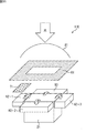
- FIG. 15 shows a schematic perspective view of the configuration of the pixel 11E provided in the surface irradiation type imaging device 1.
- An on-chip lens 81 is provided for each pixel 11E, and light incident through the on-chip lens 81 passes through the opening of the light shielding film 61 laminated on the wiring layer side of the semiconductor substrate on which the PD 21 is provided. The PD 21 is irradiated.
- charge storage units 82-1 to 82-3 are provided in three directions with respect to the PD 21, and a reset drain 83 is provided in the remaining one direction.
- the charge accumulating units 82-1 to 82-3 correspond to, for example, the charge accumulating gates 32-1 to 32-3 (see FIG. 2) and are charged from the PD 21 by the driving method described with reference to FIG. Charges are transferred to the storage units 82-1 to 82-3.
- the reset drain 83 is used to discharge the charge of the PD 21 via the anti-blooming gate 23 (see FIG. 2).
- the pixel 11E when the pixel 11E is configured to provide the capacitor 71 (see FIG. 5) instead of the charge storage portion 82-1, the gap between the light shielding film 61 and the semiconductor substrate on which the PD 21 is formed.
- the capacitor 71 is disposed in the wiring layer.
- the PD 21 and the charge storage units 82-1 to 82-3 are arranged on the same plane.
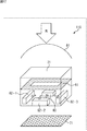
- FIG. 16 shows a schematic perspective view of the configuration of the pixel 11F provided in the back-illuminated image sensor 1.
- An on-chip lens 81 is provided for each pixel 11F, and light incident through the on-chip lens 81 is applied to the PD 21.
- a light shielding film 61 is laminated on the surface side of the PD 21 (the side facing downward in FIG. 16), and the charge storage units 82-1 to 82-3 and the reset drain 83 are shielded from light by the light shielding film 61.
- the charge storage units 82-1 to 82-3 and the reset drain 83 are arranged on the front surface side of the semiconductor substrate on which the PD 21 is provided on the back surface so as to overlap the PD 21 in plan view.
- the PD 21 and the charge storage units 82-1 to 82-3 are not arranged on the same plane.
- the area 82 to 82-3 can be designed to be larger than that of the pixel 11E in FIG.
- the size of the pixel 11F can be reduced as a whole. That is, since many portions on the back side can be used for the arrangement of the charge storage portions 82-1 to 82-3, the pixel 11F can be miniaturized. Furthermore, since the aperture ratio of the PD 21 can be increased without being affected by the charge storage units 82-1 to 82-3, the light receiving sensitivity can be improved.
- FIG. 17 shows a schematic perspective view of the configuration of the pixel 11G provided in the back-illuminated imaging device 1.
- the pixel 11G is obtained by adding a capacitor 71 to the structure of the pixel 11F in FIG.
- the capacitor 71 can be disposed only below the light shielding film 61 (that is, cannot be disposed in the opening). There was a restriction that the capacity was reduced.
- the pixel 11G there is no such restriction, and the entire area of the pixel 11G can be used for the capacitor 71. Therefore, in the pixel 11G, it is possible to increase the area and capacity of the capacitor 71 without affecting the light receiving sensitivity of the PD 21.
- the exposure times for short accumulation, medium accumulation, and long accumulation are repeated substantially the same over the light receiving period of one frame.
- the image pickup device 1 can be driven so that the exposure time of long accumulation, intermediate accumulation, and short accumulation becomes longer as the light exposure period of one frame comes later.
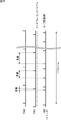
- FIG. 18 shows a first modification of the driving method.
- FIG. 18 exemplifies a long accumulation exposure time, and the exposure time is logarithmically increased as it comes later in the light receiving period of one frame.
- FIG. 19 shows a driving method without the anti-blooming gate 23 as a second modification of the driving method.
- FIG. 19 exemplifies a long accumulation exposure time, and the exposure time is logarithmically increased as it comes later in the light receiving period of one frame.
- the imaging device 1 even if the cycle for repeating the exposure time is not substantially the same, if the exposure ratio after accumulation is constant among short accumulation, intermediate accumulation, and long accumulation, HDR synthesis can be performed. it can. Even if the exposure ratio after accumulation and accumulation is irregular, the effect on the HDR image that is finally obtained can be reduced by performing HDR synthesis with the ratio corrected. For example, a better HDR image can be obtained if other effects more effective than the influence can be obtained.
- the imaging device 1 can employ a driving method (hereinafter referred to as nonlinear burst driving as appropriate) in which the exposure ratio is constant and the interval is logarithmically extended.
- non-linear burst driving with a storage time distribution that is logarithmically distributed in the time axis direction is compared to a conventional electronic shutter that cannot achieve both smoothness and crispness that only exposes the last moment of one frame. It is effective to adopt.
- exposure control close to the logarithmic response characteristic of the human eye is performed, so that an electronic shutter that achieves both smoothness and a crisp feeling without moving object blur can be realized. That is, by using a non-linear burst distribution drive, the same logarithmic sensitivity characteristic as the response characteristic of the human eye can be realized, and a moving image that can be smoothly reproduced (reproduced smoothly and smoothly) with respect to a moving subject is captured. be able to.
- the imaging device 1 including the pixel 11 of each embodiment as described above is, for example, an imaging system such as a digital still camera or a digital video camera, a mobile phone having an imaging function, or other having an imaging function.
- the present invention can be applied to various electronic devices such as these devices.
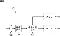
- FIG. 20 is a block diagram illustrating a configuration example of an imaging device mounted on an electronic device.
- the imaging device 101 includes an optical system 102, an imaging element 103, a signal processing circuit 104, a monitor 105, and a memory 106, and can capture still images and moving images.
- the optical system 102 includes one or more lenses, guides image light (incident light) from a subject to the image sensor 103, and forms an image on a light receiving surface (sensor unit) of the image sensor 103.
- the image sensor 103 As the image sensor 103, the image sensor 1 including the pixel 11 of each embodiment described above is applied. In the image sensor 103, electrons are accumulated for a certain period according to an image formed on the light receiving surface via the optical system 102. Then, a signal corresponding to the electrons accumulated in the image sensor 103 is supplied to the signal processing circuit 104.
- the signal processing circuit 104 performs various signal processing on the pixel signal output from the image sensor 103.
- An image (image data) obtained by performing signal processing by the signal processing circuit 104 is supplied to the monitor 105 and displayed, or supplied to the memory 106 and stored (recorded).
- the imaging apparatus 101 configured as described above, it is possible to capture a higher quality HDR image by applying the imaging element 1 including the pixel 11 of each embodiment described above.
- this technique can also take the following structures.
- (1) A pixel region in which a plurality of pixels each having a photoelectric conversion unit that converts incident light into electric charge by photoelectric conversion and stores the charge, and two or more charge storage units that store charge transferred from the photoelectric conversion unit;
- An image pickup device comprising: a drive unit that drives the pixels so as to repeat transfer of charges of different exposure times from the photoelectric conversion unit to two or more charge storage units during a light receiving period of one frame.
- the long-time exposure charge is transferred to the charge storage unit having the smaller charge storage capacity, and the short-time exposure charge is transferred to the charge storage unit having the larger charge storage capacity.
- the image sensor according to (1) or (2) wherein the image sensor is transferred.
- a potential is set such that charges overflowing from the photoelectric conversion unit are discharged to the charge storage unit having a smaller charge storage capacity during the exposure period of the pixel.
- the driving unit performs driving so that an exposure time of charges transferred to each of the two or more charge storage units is substantially the same for each of the charge storage units during the light receiving period of one frame.
- the imaging device according to any one of 1) to (8).
- the driving unit performs driving so that the exposure time of the charges transferred to each of the two or more charge storage units is substantially the same over the light receiving period of one frame.
- (1) to (9) The imaging device according to any one of the above.
- the driving unit drives the exposure unit so that an exposure time of a charge transferred to each of the two or more charge storage units becomes longer as the time after the light receiving period of one frame is increased.
- the imaging device according to any one of the above.
- the drive unit repeats, during a light receiving period of one frame, transferring charges of different exposure times from the photoelectric conversion unit to two or more charge storage units.
- Electronic equipment provided.
Landscapes
- Engineering & Computer Science (AREA)
- Multimedia (AREA)
- Signal Processing (AREA)
- Transforming Light Signals Into Electric Signals (AREA)
- Solid State Image Pick-Up Elements (AREA)
Abstract
Description
(1)
入射した光を光電変換により電荷に変換して蓄積する光電変換部、および前記光電変換部から転送される電荷を蓄積する2つ以上の電荷蓄積部を有する画素が複数配置されてなる画素領域と、
それぞれ異なる露光時間の電荷を、2つ以上の前記電荷蓄積部に前記光電変換部から転送することを、1フレームの受光期間中に繰り返すように前記画素を駆動する駆動部と
を備える撮像素子。
(2)
2つ以上の前記電荷蓄積部は、それぞれ電荷蓄積可能容量が異なる
上記(1)に記載の撮像素子。
(3)
2つ以上の前記電荷蓄積部のうち、電荷蓄積容量が少ない方の前記電荷蓄積部に長時間露光の電荷が転送され、電荷蓄積容量が大きい方の前記電荷蓄積部に短時間露光の電荷が転送される
上記(1)または(2)に記載の撮像素子。
(4)
前記画素の露光期間中に、前記光電変換部から溢れ出る電荷を排出するアンチブルーミングゲート
をさらに備える上記(1)から(3)までのいずれかに記載の撮像素子。
(5)
前記画素の露光期間中に、前記光電変換部から溢れ出る電荷が、電荷蓄積容量が小さい方の前記電荷蓄積部に排出されるように電位が設定されている
上記(3)に記載の撮像素子。
(6)
電荷蓄積容量が大きい方の前記電荷蓄積部には、拡散接合を経由したキャパシタ構造の蓄積部を使用する
上記(3)から(5)までのいずれかに記載の撮像素子。
(7)
電荷蓄積容量が小さい方の前記電荷蓄積部には、遮光されたフォトダイオード構造の蓄積部を使用する
上記(3)から(6)までのいずれかに記載の撮像素子。
(8)
前記光電変換部で発生した電荷を電圧に変換する電荷電圧変換部をさらに備え、
2つ以上の前記電荷蓄積部から共通の前記電荷電圧変換部に電荷が転送され、2つ以上の前記電荷蓄積部で前記電荷電圧変換部以降の構造を共有する
上記(1)から(7)までのいずれかに記載の撮像素子。
(9)
前記駆動部は、1フレームの受光期間中において、2つ以上の前記電荷蓄積部それぞれに対して転送する電荷の露光時間が、前記電荷蓄積部ごとに略同一となるように駆動を行う
上記(1)から(8)までのいずれかに記載の撮像素子。
(10)
前記駆動部は、2つ以上の前記電荷蓄積部それぞれに対して転送する電荷の露光時間が、1フレームの受光期間に亘って略同一となるように駆動を行う
上記(1)から(9)までのいずれかに記載の撮像素子。
(11)
前記駆動部は、2つ以上の前記電荷蓄積部それぞれに対して転送する電荷の露光時間が、1フレームの受光期間中の後になるに従い長くなるように駆動を行う
上記(1)から(9)までのいずれかに記載の撮像素子。
(12)
入射した光を光電変換により電荷に変換して蓄積する光電変換部、および前記光電変換部から転送される電荷を蓄積する2つ以上の電荷蓄積部を有する画素が複数配置されてなる画素領域と、前記画素を駆動する駆動部とを備える撮像素子の駆動方法において、
前記駆動部は、それぞれ異なる露光時間の電荷を、2つ以上の前記電荷蓄積部に前記光電変換部から転送することを、1フレームの受光期間中に繰り返す
駆動方法。
(13)
入射した光を光電変換により電荷に変換して蓄積する光電変換部、および前記光電変換部から転送される電荷を蓄積する2つ以上の電荷蓄積部を有する画素が複数配置されてなる画素領域と、
それぞれ異なる露光時間の電荷を、2つ以上の前記電荷蓄積部に前記光電変換部から転送することを、1フレームの受光期間中に繰り返すように前記画素を駆動する駆動部と
を有する撮像素子を備える電子機器。
Claims (13)
- 入射した光を光電変換により電荷に変換して蓄積する光電変換部、および前記光電変換部から転送される電荷を蓄積する2つ以上の電荷蓄積部を有する画素が複数配置されてなる画素領域と、
それぞれ異なる露光時間の電荷を、2つ以上の前記電荷蓄積部に前記光電変換部から転送することを、1フレームの受光期間中に繰り返すように前記画素を駆動する駆動部と
を備える撮像素子。 - 2つ以上の前記電荷蓄積部は、それぞれ電荷蓄積可能容量が異なる
請求項1に記載の撮像素子。 - 2つ以上の前記電荷蓄積部のうち、電荷蓄積容量が少ない方の前記電荷蓄積部に長時間露光の電荷が転送され、電荷蓄積容量が大きい方の前記電荷蓄積部に短時間露光の電荷が転送される
請求項2に記載の撮像素子。 - 前記画素の露光期間中に、前記光電変換部から溢れ出る電荷を排出するアンチブルーミングゲート
をさらに備える請求項1に記載の撮像素子。 - 前記画素の露光期間中に、前記光電変換部から溢れ出る電荷が、電荷蓄積容量が小さい方の前記電荷蓄積部に排出されるように電位が設定されている
請求項3に記載の撮像素子。 - 電荷蓄積容量が大きい方の前記電荷蓄積部には、拡散接合を経由したキャパシタ構造の蓄積部を使用する
請求項3に記載の撮像素子。 - 電荷蓄積容量が小さい方の前記電荷蓄積部には、遮光されたフォトダイオード構造の蓄積部を使用する
請求項3に記載の撮像素子。 - 前記光電変換部で発生した電荷を電圧に変換する電荷電圧変換部をさらに備え、
2つ以上の前記電荷蓄積部から共通の前記電荷電圧変換部に電荷が転送され、2つ以上の前記電荷蓄積部で前記電荷電圧変換部以降の構造を共有する
請求項1に記載の撮像素子。 - 前記駆動部は、1フレームの受光期間中において、2つ以上の前記電荷蓄積部それぞれに対して転送する電荷の露光時間が、前記電荷蓄積部ごとに略同一となるように駆動を行う
請求項1に記載の撮像素子。 - 前記駆動部は、2つ以上の前記電荷蓄積部それぞれに対して転送する電荷の露光時間が、1フレームの受光期間に亘って略同一となるように駆動を行う
請求項1に記載の撮像素子。 - 前記駆動部は、2つ以上の前記電荷蓄積部それぞれに対して転送する電荷の露光時間が、1フレームの受光期間中の後になるに従い長くなるように駆動を行う
請求項1に記載の撮像素子。 - 入射した光を光電変換により電荷に変換して蓄積する光電変換部、および前記光電変換部から転送される電荷を蓄積する2つ以上の電荷蓄積部を有する画素が複数配置されてなる画素領域と、前記画素を駆動する駆動部とを備える撮像素子の駆動方法において、
前記駆動部は、それぞれ異なる露光時間の電荷を、2つ以上の前記電荷蓄積部に前記光電変換部から転送することを、1フレームの受光期間中に繰り返す
駆動方法。 - 入射した光を光電変換により電荷に変換して蓄積する光電変換部、および前記光電変換部から転送される電荷を蓄積する2つ以上の電荷蓄積部を有する画素が複数配置されてなる画素領域と、
それぞれ異なる露光時間の電荷を、2つ以上の前記電荷蓄積部に前記光電変換部から転送することを、1フレームの受光期間中に繰り返すように前記画素を駆動する駆動部と
を有する撮像素子を備える電子機器。
Priority Applications (4)
| Application Number | Priority Date | Filing Date | Title |
|---|---|---|---|
| JP2016574723A JP6808495B2 (ja) | 2015-02-13 | 2016-01-29 | 撮像素子、駆動方法、および電子機器 |
| US15/546,496 US10264197B2 (en) | 2015-02-13 | 2016-01-29 | Imaging device, driving method, and electronic apparatus |
| US16/286,385 US10674100B2 (en) | 2015-02-13 | 2019-02-26 | Imaging device, driving method, and electronic apparatus |
| US16/842,436 US11006059B2 (en) | 2015-02-13 | 2020-04-07 | Imaging device, driving method, and electronic apparatus |
Applications Claiming Priority (2)
| Application Number | Priority Date | Filing Date | Title |
|---|---|---|---|
| JP2015026497 | 2015-02-13 | ||
| JP2015-026497 | 2015-02-13 |
Related Child Applications (2)
| Application Number | Title | Priority Date | Filing Date |
|---|---|---|---|
| US15/546,496 A-371-Of-International US10264197B2 (en) | 2015-02-13 | 2016-01-29 | Imaging device, driving method, and electronic apparatus |
| US16/286,385 Continuation US10674100B2 (en) | 2015-02-13 | 2019-02-26 | Imaging device, driving method, and electronic apparatus |
Publications (1)
| Publication Number | Publication Date |
|---|---|
| WO2016129410A1 true WO2016129410A1 (ja) | 2016-08-18 |
Family
ID=56614674
Family Applications (1)
| Application Number | Title | Priority Date | Filing Date |
|---|---|---|---|
| PCT/JP2016/052592 Ceased WO2016129410A1 (ja) | 2015-02-13 | 2016-01-29 | 撮像素子、駆動方法、および電子機器 |
Country Status (3)
| Country | Link |
|---|---|
| US (3) | US10264197B2 (ja) |
| JP (1) | JP6808495B2 (ja) |
| WO (1) | WO2016129410A1 (ja) |
Cited By (7)
| Publication number | Priority date | Publication date | Assignee | Title |
|---|---|---|---|---|
| CN110720211A (zh) * | 2017-06-23 | 2020-01-21 | 高通股份有限公司 | 针对hdr图像和视频使用相同像素捕获短曝光数据和长曝光数据两者 |
| CN111373745A (zh) * | 2017-11-22 | 2020-07-03 | 索尼半导体解决方案公司 | 固态摄像元件和电子设备 |
| WO2020178920A1 (ja) * | 2019-03-01 | 2020-09-10 | 株式会社ブルックマンテクノロジ | 距離画像撮像装置および距離画像撮像装置による距離画像撮像方法 |
| KR20220100568A (ko) * | 2019-11-15 | 2022-07-15 | 소니 세미컨덕터 솔루션즈 가부시키가이샤 | 촬상 장치 |
| JP2022537117A (ja) * | 2019-06-21 | 2022-08-24 | ザ ガバニング カウンシル オブ ザ ユニバーシティ オブ トロント | 画素パラメータの画素単位の符号化を用いて画像ダイナミックレンジを拡張するための方法およびシステム |
| JP2022543459A (ja) * | 2019-08-08 | 2022-10-12 | マイクロソフト テクノロジー ライセンシング,エルエルシー | Tofピクセルを用いたhdr可視光イメージング |
| US12116285B2 (en) | 2018-10-05 | 2024-10-15 | Fuji Chemical Industries Co., Ltd. | Porous silica particle composition |
Families Citing this family (10)
| Publication number | Priority date | Publication date | Assignee | Title |
|---|---|---|---|---|
| US10313600B2 (en) * | 2015-10-13 | 2019-06-04 | Canon Kabushiki Kaisha | Imaging device capable of simultaneously capturing of a motion image and a static image and imaging method |
| US10165213B2 (en) | 2015-11-16 | 2018-12-25 | Taiwan Semiconductor Manufacturing Co., Ltd. | Image sensor including pixel circuits |
| US9942492B2 (en) * | 2016-06-16 | 2018-04-10 | Semiconductor Components Industries, Llc | Image sensors having high dynamic range functionalities |
| US10116891B2 (en) * | 2016-10-07 | 2018-10-30 | Stmicroelectronics (Research & Development) Limited | Image sensor having stacked imaging and digital wafers where digital wafer has stacked capacitors and logic circuitry |
| US10263021B2 (en) | 2016-12-12 | 2019-04-16 | Stmicroelectronics (Research & Development) Limited | Global shutter pixels having shared isolated storage capacitors within an isolation structure surrounding the perimeter of a pixel array |
| CN108337409B (zh) * | 2017-01-19 | 2021-06-22 | 松下知识产权经营株式会社 | 摄像装置及照相机系统 |
| JP7157529B2 (ja) * | 2017-12-25 | 2022-10-20 | キヤノン株式会社 | 撮像装置、撮像システム、および撮像装置の駆動方法 |
| CN110832846B (zh) * | 2018-08-31 | 2022-04-08 | 深圳市大疆创新科技有限公司 | 像素单元、图像传感器及其运行方法、摄像装置 |
| US10756129B2 (en) * | 2019-01-10 | 2020-08-25 | Semiconductor Components Industries, Llc | Image sensors having imaging pixels with ring-shaped gates |
| KR102929692B1 (ko) | 2020-09-16 | 2026-02-20 | 삼성전자주식회사 | 다중 전송을 이용하는 이미지 센서 및 이의 동작 방법 |
Citations (4)
| Publication number | Priority date | Publication date | Assignee | Title |
|---|---|---|---|---|
| JPH05268533A (ja) * | 1992-03-24 | 1993-10-15 | Matsushita Electric Ind Co Ltd | イメージセンサ |
| JP2004111590A (ja) * | 2002-09-18 | 2004-04-08 | Sony Corp | 固体撮像装置およびその駆動制御方法 |
| JP2008028678A (ja) * | 2006-07-20 | 2008-02-07 | Pentax Corp | 撮像素子 |
| JP2013055610A (ja) * | 2011-09-06 | 2013-03-21 | Olympus Imaging Corp | 撮像装置 |
Family Cites Families (10)
| Publication number | Priority date | Publication date | Assignee | Title |
|---|---|---|---|---|
| JPS5521682B2 (ja) | 1973-10-29 | 1980-06-11 | ||
| US8392552B2 (en) * | 2000-09-28 | 2013-03-05 | Vig Acquisitions Ltd., L.L.C. | System and method for providing configurable security monitoring utilizing an integrated information system |
| US7078746B2 (en) * | 2003-07-15 | 2006-07-18 | Micron Technology, Inc. | Image sensor with floating diffusion gate capacitor |
| US7825966B2 (en) * | 2007-06-29 | 2010-11-02 | Omnivision Technologies, Inc. | High dynamic range sensor with blooming drain |
| JP2010279016A (ja) * | 2009-04-30 | 2010-12-09 | Sony Corp | 固体撮像素子とその駆動方法および撮像装置 |
| US8279328B2 (en) * | 2009-07-15 | 2012-10-02 | Tower Semiconductor Ltd. | CMOS image sensor with wide (intra-scene) dynamic range |
| JP5625284B2 (ja) * | 2009-08-10 | 2014-11-19 | ソニー株式会社 | 固体撮像装置、固体撮像装置の駆動方法および電子機器 |
| JP5521682B2 (ja) | 2010-02-26 | 2014-06-18 | ソニー株式会社 | 固体撮像装置、固体撮像装置の駆動方法、及び、電子機器 |
| US9118883B2 (en) * | 2011-11-28 | 2015-08-25 | Semiconductor Components Industries, Llc | High dynamic range imaging with multi-storage pixels |
| US20140246561A1 (en) * | 2013-03-04 | 2014-09-04 | Omnivision Technologies, Inc. | High dynamic range pixel having a plurality of photodiodes with a single implant |
-
2016
- 2016-01-29 WO PCT/JP2016/052592 patent/WO2016129410A1/ja not_active Ceased
- 2016-01-29 US US15/546,496 patent/US10264197B2/en active Active
- 2016-01-29 JP JP2016574723A patent/JP6808495B2/ja not_active Expired - Fee Related
-
2019
- 2019-02-26 US US16/286,385 patent/US10674100B2/en not_active Expired - Fee Related
-
2020
- 2020-04-07 US US16/842,436 patent/US11006059B2/en active Active
Patent Citations (4)
| Publication number | Priority date | Publication date | Assignee | Title |
|---|---|---|---|---|
| JPH05268533A (ja) * | 1992-03-24 | 1993-10-15 | Matsushita Electric Ind Co Ltd | イメージセンサ |
| JP2004111590A (ja) * | 2002-09-18 | 2004-04-08 | Sony Corp | 固体撮像装置およびその駆動制御方法 |
| JP2008028678A (ja) * | 2006-07-20 | 2008-02-07 | Pentax Corp | 撮像素子 |
| JP2013055610A (ja) * | 2011-09-06 | 2013-03-21 | Olympus Imaging Corp | 撮像装置 |
Cited By (18)
| Publication number | Priority date | Publication date | Assignee | Title |
|---|---|---|---|---|
| CN110720211A (zh) * | 2017-06-23 | 2020-01-21 | 高通股份有限公司 | 针对hdr图像和视频使用相同像素捕获短曝光数据和长曝光数据两者 |
| CN111373745B (zh) * | 2017-11-22 | 2023-03-24 | 索尼半导体解决方案公司 | 固态摄像元件和电子设备 |
| CN111373745A (zh) * | 2017-11-22 | 2020-07-03 | 索尼半导体解决方案公司 | 固态摄像元件和电子设备 |
| US12506976B2 (en) | 2017-11-22 | 2025-12-23 | Sony Semiconductor Solutions Corporation | Solid-state imaging device and electronic apparatus |
| US12022209B2 (en) | 2017-11-22 | 2024-06-25 | Sony Semiconductor Solutions Corporation | Solid-state imaging device and electronic apparatus |
| US11936994B2 (en) | 2017-11-22 | 2024-03-19 | Sony Semiconductor Solutions Corporation | Solid-state imaging device and electronic apparatus |
| US11877074B2 (en) | 2017-11-22 | 2024-01-16 | Sony Semiconductor Solutions Corporation | Solid-state imaging device and electronic apparatus |
| US12116285B2 (en) | 2018-10-05 | 2024-10-15 | Fuji Chemical Industries Co., Ltd. | Porous silica particle composition |
| US11336854B2 (en) | 2019-03-01 | 2022-05-17 | Brookman Technology, Inc. | Distance image capturing apparatus and distance image capturing method using distance image capturing apparatus |
| JP6825164B1 (ja) * | 2019-03-01 | 2021-02-03 | 株式会社ブルックマンテクノロジ | 距離画像撮像装置および距離画像撮像装置による距離画像撮像方法 |
| WO2020178920A1 (ja) * | 2019-03-01 | 2020-09-10 | 株式会社ブルックマンテクノロジ | 距離画像撮像装置および距離画像撮像装置による距離画像撮像方法 |
| JP2022537117A (ja) * | 2019-06-21 | 2022-08-24 | ザ ガバニング カウンシル オブ ザ ユニバーシティ オブ トロント | 画素パラメータの画素単位の符号化を用いて画像ダイナミックレンジを拡張するための方法およびシステム |
| JP7610269B2 (ja) | 2019-06-21 | 2025-01-08 | ザ ガバニング カウンシル オブ ザ ユニバーシティ オブ トロント | 画素パラメータの画素単位の符号化を用いて画像ダイナミックレンジを拡張するための方法およびシステム |
| JP2022543459A (ja) * | 2019-08-08 | 2022-10-12 | マイクロソフト テクノロジー ライセンシング,エルエルシー | Tofピクセルを用いたhdr可視光イメージング |
| JP7585302B2 (ja) | 2019-08-08 | 2024-11-18 | マイクロソフト テクノロジー ライセンシング,エルエルシー | Tofピクセルを用いたhdr可視光イメージング |
| KR20220100568A (ko) * | 2019-11-15 | 2022-07-15 | 소니 세미컨덕터 솔루션즈 가부시키가이샤 | 촬상 장치 |
| KR102786633B1 (ko) | 2019-11-15 | 2025-03-28 | 소니 세미컨덕터 솔루션즈 가부시키가이샤 | 촬상 장치 |
| US12396277B2 (en) | 2019-11-15 | 2025-08-19 | Sony Semiconductor Solutions Corporation | Imaging device |
Also Published As
| Publication number | Publication date |
|---|---|
| US10674100B2 (en) | 2020-06-02 |
| US20190191113A1 (en) | 2019-06-20 |
| US10264197B2 (en) | 2019-04-16 |
| US20200236308A1 (en) | 2020-07-23 |
| US20180020172A1 (en) | 2018-01-18 |
| JPWO2016129410A1 (ja) | 2017-11-24 |
| US11006059B2 (en) | 2021-05-11 |
| JP6808495B2 (ja) | 2021-01-06 |
Similar Documents
| Publication | Publication Date | Title |
|---|---|---|
| JP6808495B2 (ja) | 撮像素子、駆動方法、および電子機器 | |
| US10313613B2 (en) | High dynamic range image sensors with flicker and fixed pattern noise mitigation | |
| US10194110B2 (en) | Solid-state imaging device, imaging device, and signal reading method | |
| US8184188B2 (en) | Methods and apparatus for high dynamic operation of a pixel cell | |
| CN202395873U (zh) | 固体摄像器件和电子装置 | |
| JP5516960B2 (ja) | 固体撮像装置、固体撮像装置の駆動方法、および、電子機器 | |
| US8421894B2 (en) | Solid-state image pickup device and control method thereof, and camera | |
| JP4459099B2 (ja) | 固体撮像装置及びカメラ | |
| JP4973115B2 (ja) | 固体撮像装置、固体撮像装置の駆動方法および撮像装置 | |
| JP5215262B2 (ja) | 撮像装置 | |
| JP6126666B2 (ja) | 固体撮像装置及び電子機器 | |
| US9674468B2 (en) | Imaging device and driving method for solid-state image sensor with multiple different electric potentials | |
| JP5223953B2 (ja) | 固体撮像装置、固体撮像装置の駆動方法および撮像装置 | |
| JP2012195734A (ja) | 固体撮像装置、撮像装置、電子機器、及び、固体撮像装置の駆動方法 | |
| JP2007151069A (ja) | 固体撮像装置、固体撮像装置の駆動方法および撮像装置 | |
| CN103685999A (zh) | 固态图像传感器、用于固态图像传感器的控制方法以及电子装置 | |
| US8072526B2 (en) | Image sensor, imaging system, and image sensor control method | |
| US7821559B2 (en) | Photoelectric conversion apparatus provided with arrangement of plurality of pixels each having plurality of photoelectric conversion devices and accumulating unit for temporarily accumulating charges accumulated in plurality of photoelectric conversion devices | |
| JP2006093517A (ja) | 固体撮像装置 | |
| US20090237538A1 (en) | Solid-state image pickup device | |
| JP2017005612A (ja) | 撮像装置、撮像方法、並びにプログラム | |
| JP2013106231A (ja) | 撮像装置 | |
| JP5402993B2 (ja) | 固体撮像装置、固体撮像装置の駆動方法および電子機器 | |
| JP4840992B2 (ja) | 光電変換装置及びその制御方法並びに撮像装置 | |
| JP2010278795A (ja) | 固体撮像装置、固体撮像装置の駆動方法および電子機器 |
Legal Events
| Date | Code | Title | Description |
|---|---|---|---|
| 121 | Ep: the epo has been informed by wipo that ep was designated in this application |
Ref document number: 16749054 Country of ref document: EP Kind code of ref document: A1 |
|
| ENP | Entry into the national phase |
Ref document number: 2016574723 Country of ref document: JP Kind code of ref document: A |
|
| WWE | Wipo information: entry into national phase |
Ref document number: 15546496 Country of ref document: US |
|
| NENP | Non-entry into the national phase |
Ref country code: DE |
|
| 122 | Ep: pct application non-entry in european phase |
Ref document number: 16749054 Country of ref document: EP Kind code of ref document: A1 |