WO2016125323A1 - 半導体装置 - Google Patents
半導体装置 Download PDFInfo
- Publication number
- WO2016125323A1 WO2016125323A1 PCT/JP2015/068033 JP2015068033W WO2016125323A1 WO 2016125323 A1 WO2016125323 A1 WO 2016125323A1 JP 2015068033 W JP2015068033 W JP 2015068033W WO 2016125323 A1 WO2016125323 A1 WO 2016125323A1
- Authority
- WO
- WIPO (PCT)
- Prior art keywords
- gate
- termination circuit
- finger
- fingers
- semiconductor device
- Prior art date
Links
- 239000004065 semiconductor Substances 0.000 title claims abstract description 37
- 230000001939 inductive effect Effects 0.000 claims abstract description 19
- 239000000758 substrate Substances 0.000 claims abstract description 8
- 239000003990 capacitor Substances 0.000 claims description 32
- 230000005540 biological transmission Effects 0.000 claims description 17
- 238000004458 analytical method Methods 0.000 description 40
- 230000000694 effects Effects 0.000 description 16
- 230000006872 improvement Effects 0.000 description 9
- 238000000034 method Methods 0.000 description 5
- 238000010586 diagram Methods 0.000 description 4
- 230000010355 oscillation Effects 0.000 description 4
- 230000005669 field effect Effects 0.000 description 3
- 238000004364 calculation method Methods 0.000 description 2
- 238000004519 manufacturing process Methods 0.000 description 2
- 230000009291 secondary effect Effects 0.000 description 2
- 229910001218 Gallium arsenide Inorganic materials 0.000 description 1
- 230000002411 adverse Effects 0.000 description 1
- 238000011156 evaluation Methods 0.000 description 1
- 238000012986 modification Methods 0.000 description 1
- 230000004048 modification Effects 0.000 description 1
- 230000003071 parasitic effect Effects 0.000 description 1
- 230000008569 process Effects 0.000 description 1
- 230000009467 reduction Effects 0.000 description 1
- 230000006641 stabilisation Effects 0.000 description 1
- 238000011105 stabilization Methods 0.000 description 1
Images


Classifications
-
- H—ELECTRICITY
- H01—ELECTRIC ELEMENTS
- H01L—SEMICONDUCTOR DEVICES NOT COVERED BY CLASS H10
- H01L29/00—Semiconductor devices adapted for rectifying, amplifying, oscillating or switching, or capacitors or resistors with at least one potential-jump barrier or surface barrier, e.g. PN junction depletion layer or carrier concentration layer; Details of semiconductor bodies or of electrodes thereof ; Multistep manufacturing processes therefor
- H01L29/66—Types of semiconductor device ; Multistep manufacturing processes therefor
- H01L29/68—Types of semiconductor device ; Multistep manufacturing processes therefor controllable by only the electric current supplied, or only the electric potential applied, to an electrode which does not carry the current to be rectified, amplified or switched
- H01L29/76—Unipolar devices, e.g. field effect transistors
- H01L29/772—Field effect transistors
- H01L29/78—Field effect transistors with field effect produced by an insulated gate
- H01L29/7831—Field effect transistors with field effect produced by an insulated gate with multiple gate structure
-
- H—ELECTRICITY
- H01—ELECTRIC ELEMENTS
- H01L—SEMICONDUCTOR DEVICES NOT COVERED BY CLASS H10
- H01L21/00—Processes or apparatus adapted for the manufacture or treatment of semiconductor or solid state devices or of parts thereof
- H01L21/70—Manufacture or treatment of devices consisting of a plurality of solid state components formed in or on a common substrate or of parts thereof; Manufacture of integrated circuit devices or of parts thereof
- H01L21/77—Manufacture or treatment of devices consisting of a plurality of solid state components or integrated circuits formed in, or on, a common substrate
- H01L21/78—Manufacture or treatment of devices consisting of a plurality of solid state components or integrated circuits formed in, or on, a common substrate with subsequent division of the substrate into plural individual devices
- H01L21/82—Manufacture or treatment of devices consisting of a plurality of solid state components or integrated circuits formed in, or on, a common substrate with subsequent division of the substrate into plural individual devices to produce devices, e.g. integrated circuits, each consisting of a plurality of components
- H01L21/822—Manufacture or treatment of devices consisting of a plurality of solid state components or integrated circuits formed in, or on, a common substrate with subsequent division of the substrate into plural individual devices to produce devices, e.g. integrated circuits, each consisting of a plurality of components the substrate being a semiconductor, using silicon technology
-
- H—ELECTRICITY
- H01—ELECTRIC ELEMENTS
- H01L—SEMICONDUCTOR DEVICES NOT COVERED BY CLASS H10
- H01L23/00—Details of semiconductor or other solid state devices
- H01L23/48—Arrangements for conducting electric current to or from the solid state body in operation, e.g. leads, terminal arrangements ; Selection of materials therefor
- H01L23/482—Arrangements for conducting electric current to or from the solid state body in operation, e.g. leads, terminal arrangements ; Selection of materials therefor consisting of lead-in layers inseparably applied to the semiconductor body
- H01L23/4821—Bridge structure with air gap
-
- H—ELECTRICITY
- H01—ELECTRIC ELEMENTS
- H01L—SEMICONDUCTOR DEVICES NOT COVERED BY CLASS H10
- H01L23/00—Details of semiconductor or other solid state devices
- H01L23/48—Arrangements for conducting electric current to or from the solid state body in operation, e.g. leads, terminal arrangements ; Selection of materials therefor
- H01L23/482—Arrangements for conducting electric current to or from the solid state body in operation, e.g. leads, terminal arrangements ; Selection of materials therefor consisting of lead-in layers inseparably applied to the semiconductor body
- H01L23/4824—Pads with extended contours, e.g. grid structure, branch structure, finger structure
-
- H—ELECTRICITY
- H01—ELECTRIC ELEMENTS
- H01L—SEMICONDUCTOR DEVICES NOT COVERED BY CLASS H10
- H01L23/00—Details of semiconductor or other solid state devices
- H01L23/58—Structural electrical arrangements for semiconductor devices not otherwise provided for, e.g. in combination with batteries
- H01L23/64—Impedance arrangements
- H01L23/66—High-frequency adaptations
-
- H—ELECTRICITY
- H01—ELECTRIC ELEMENTS
- H01L—SEMICONDUCTOR DEVICES NOT COVERED BY CLASS H10
- H01L27/00—Devices consisting of a plurality of semiconductor or other solid-state components formed in or on a common substrate
- H01L27/02—Devices consisting of a plurality of semiconductor or other solid-state components formed in or on a common substrate including semiconductor components specially adapted for rectifying, oscillating, amplifying or switching and having at least one potential-jump barrier or surface barrier; including integrated passive circuit elements with at least one potential-jump barrier or surface barrier
- H01L27/04—Devices consisting of a plurality of semiconductor or other solid-state components formed in or on a common substrate including semiconductor components specially adapted for rectifying, oscillating, amplifying or switching and having at least one potential-jump barrier or surface barrier; including integrated passive circuit elements with at least one potential-jump barrier or surface barrier the substrate being a semiconductor body
- H01L27/06—Devices consisting of a plurality of semiconductor or other solid-state components formed in or on a common substrate including semiconductor components specially adapted for rectifying, oscillating, amplifying or switching and having at least one potential-jump barrier or surface barrier; including integrated passive circuit elements with at least one potential-jump barrier or surface barrier the substrate being a semiconductor body including a plurality of individual components in a non-repetitive configuration
- H01L27/0611—Devices consisting of a plurality of semiconductor or other solid-state components formed in or on a common substrate including semiconductor components specially adapted for rectifying, oscillating, amplifying or switching and having at least one potential-jump barrier or surface barrier; including integrated passive circuit elements with at least one potential-jump barrier or surface barrier the substrate being a semiconductor body including a plurality of individual components in a non-repetitive configuration integrated circuits having a two-dimensional layout of components without a common active region
- H01L27/0617—Devices consisting of a plurality of semiconductor or other solid-state components formed in or on a common substrate including semiconductor components specially adapted for rectifying, oscillating, amplifying or switching and having at least one potential-jump barrier or surface barrier; including integrated passive circuit elements with at least one potential-jump barrier or surface barrier the substrate being a semiconductor body including a plurality of individual components in a non-repetitive configuration integrated circuits having a two-dimensional layout of components without a common active region comprising components of the field-effect type
- H01L27/0629—Devices consisting of a plurality of semiconductor or other solid-state components formed in or on a common substrate including semiconductor components specially adapted for rectifying, oscillating, amplifying or switching and having at least one potential-jump barrier or surface barrier; including integrated passive circuit elements with at least one potential-jump barrier or surface barrier the substrate being a semiconductor body including a plurality of individual components in a non-repetitive configuration integrated circuits having a two-dimensional layout of components without a common active region comprising components of the field-effect type in combination with diodes, or resistors, or capacitors
-
- H—ELECTRICITY
- H01—ELECTRIC ELEMENTS
- H01L—SEMICONDUCTOR DEVICES NOT COVERED BY CLASS H10
- H01L29/00—Semiconductor devices adapted for rectifying, amplifying, oscillating or switching, or capacitors or resistors with at least one potential-jump barrier or surface barrier, e.g. PN junction depletion layer or carrier concentration layer; Details of semiconductor bodies or of electrodes thereof ; Multistep manufacturing processes therefor
- H01L29/66—Types of semiconductor device ; Multistep manufacturing processes therefor
- H01L29/68—Types of semiconductor device ; Multistep manufacturing processes therefor controllable by only the electric current supplied, or only the electric potential applied, to an electrode which does not carry the current to be rectified, amplified or switched
- H01L29/76—Unipolar devices, e.g. field effect transistors
- H01L29/772—Field effect transistors
- H01L29/80—Field effect transistors with field effect produced by a PN or other rectifying junction gate, i.e. potential-jump barrier
- H01L29/812—Field effect transistors with field effect produced by a PN or other rectifying junction gate, i.e. potential-jump barrier with a Schottky gate
-
- H—ELECTRICITY
- H03—ELECTRONIC CIRCUITRY
- H03F—AMPLIFIERS
- H03F1/00—Details of amplifiers with only discharge tubes, only semiconductor devices or only unspecified devices as amplifying elements
- H03F1/56—Modifications of input or output impedances, not otherwise provided for
- H03F1/565—Modifications of input or output impedances, not otherwise provided for using inductive elements
-
- H—ELECTRICITY
- H03—ELECTRONIC CIRCUITRY
- H03F—AMPLIFIERS
- H03F3/00—Amplifiers with only discharge tubes or only semiconductor devices as amplifying elements
- H03F3/189—High frequency amplifiers, e.g. radio frequency amplifiers
- H03F3/19—High frequency amplifiers, e.g. radio frequency amplifiers with semiconductor devices only
- H03F3/195—High frequency amplifiers, e.g. radio frequency amplifiers with semiconductor devices only in integrated circuits
-
- H—ELECTRICITY
- H03—ELECTRONIC CIRCUITRY
- H03F—AMPLIFIERS
- H03F3/00—Amplifiers with only discharge tubes or only semiconductor devices as amplifying elements
- H03F3/20—Power amplifiers, e.g. Class B amplifiers, Class C amplifiers
- H03F3/21—Power amplifiers, e.g. Class B amplifiers, Class C amplifiers with semiconductor devices only
- H03F3/213—Power amplifiers, e.g. Class B amplifiers, Class C amplifiers with semiconductor devices only in integrated circuits
-
- H—ELECTRICITY
- H01—ELECTRIC ELEMENTS
- H01L—SEMICONDUCTOR DEVICES NOT COVERED BY CLASS H10
- H01L2223/00—Details relating to semiconductor or other solid state devices covered by the group H01L23/00
- H01L2223/58—Structural electrical arrangements for semiconductor devices not otherwise provided for
- H01L2223/64—Impedance arrangements
- H01L2223/66—High-frequency adaptations
- H01L2223/6605—High-frequency electrical connections
- H01L2223/6611—Wire connections
-
- H—ELECTRICITY
- H01—ELECTRIC ELEMENTS
- H01L—SEMICONDUCTOR DEVICES NOT COVERED BY CLASS H10
- H01L2223/00—Details relating to semiconductor or other solid state devices covered by the group H01L23/00
- H01L2223/58—Structural electrical arrangements for semiconductor devices not otherwise provided for
- H01L2223/64—Impedance arrangements
- H01L2223/66—High-frequency adaptations
- H01L2223/6644—Packaging aspects of high-frequency amplifiers
- H01L2223/6655—Matching arrangements, e.g. arrangement of inductive and capacitive components
-
- H—ELECTRICITY
- H03—ELECTRONIC CIRCUITRY
- H03F—AMPLIFIERS
- H03F2200/00—Indexing scheme relating to amplifiers
- H03F2200/12—A bias circuit for some stages being shown using transmission lines
-
- H—ELECTRICITY
- H03—ELECTRONIC CIRCUITRY
- H03F—AMPLIFIERS
- H03F2200/00—Indexing scheme relating to amplifiers
- H03F2200/222—A circuit being added at the input of an amplifier to adapt the input impedance of the amplifier
-
- H—ELECTRICITY
- H03—ELECTRONIC CIRCUITRY
- H03F—AMPLIFIERS
- H03F2200/00—Indexing scheme relating to amplifiers
- H03F2200/451—Indexing scheme relating to amplifiers the amplifier being a radio frequency amplifier
Definitions
- the present invention relates to a semiconductor device such as a field effect transistor (FET) used in a high frequency power amplifier.
- FET field effect transistor
- Non-Patent Document 1 FET in which source fingers and drain fingers are alternately arranged in parallel with one or more gate fingers interposed therebetween.
- Non-Patent Document 1 the conventional FET has a problem that a voltage distribution due to the signal wavelength occurs in one cell. As a result, a part of the cell does not operate, and the performance of the FET may deteriorate.
- the present invention has been made to solve the above-described problems, and an object of the present invention is to provide a semiconductor device that can equalize the voltage in one cell of the semiconductor device.
- a semiconductor device includes one or more gate fingers provided in an active region on a semiconductor substrate, and source fingers and drain fingers provided in the active region and arranged alternately with the gate fingers interposed therebetween.
- the impedance is inductive at the frequency of the signal input from the input terminal of the gate finger, and is directly or indirectly connected to the gate finger at a location away from the connection position of the input terminal of the gate finger.
- a termination circuit is provided.
- the voltage in one cell of the semiconductor device can be made uniform.
- FIG. 1 It is a perspective view which shows the structure of FET which concerns on Embodiment 1 of this invention. It is a figure which shows the structure pattern of FET which concerns on Embodiment 1 of this invention. It is a figure which shows the structural example of the termination circuit in Embodiment 1 of this invention. It is a figure which shows the effect of FET which concerns on Embodiment 1 of this invention. It is a figure which shows the example of an analysis result of the voltage distribution in 1 gate finger in the conventional FET. It is a figure which shows the example of an analysis result of the voltage distribution in 1 gate finger in FET which concerns on Embodiment 1 of this invention.
- FIG. 9 is a diagram illustrating a relationship between a normalized imaginary part of input impedance and a line wavelength in the termination circuit illustrated in FIG. 8.
- FIG. 9 is a diagram illustrating a result of obtaining a lower limit and an upper limit of the line wavelength at which the imaginary part of the input impedance is positive with respect to Z 0 ⁇ C in the termination circuit illustrated in FIG. 8.
- FIG. 9 shows another structural example of the termination circuit in Embodiment 1 of this invention.
- FIG. 1 is a perspective view showing the configuration of an FET according to Embodiment 1 of the present invention.
- an FET used for a high-frequency power amplifier is described as an example of a semiconductor device, but the present invention is not limited to this.
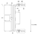
- one or more gate fingers 20 are arranged in the active region, and source fingers 30 and drain fingers 40 are alternately arranged in parallel with the gate fingers 20 in between.
- the gate finger 20, the source finger 30, and the drain finger 40 are arranged in parallel one by one.
- reference numeral 2 denotes a ground.
- the gate width of the gate finger 20 is Wgu.
- This termination circuit 60 is a circuit having an inductive impedance at the frequency of the signal input to the gate finger 20 from the input terminal 21a. In other words, the imaginary part of the input impedance is positive at the signal frequency.
- FIG. 2 is a view showing a structure pattern of the FET according to the first embodiment of the present invention.
- one gate finger 20 is arranged in the active region on the semiconductor substrate 1 of the FET, and one source finger 30 and one drain finger 40 are arranged in parallel with the gate finger 20 in between. . That is, FIG. 2 shows a case where the FET is configured as a single finger transistor.
- the source finger 30 is grounded via a source electrode 32 (corresponding to the terminal 31a shown in FIG. 1).
- the gate finger 20 is electrically connected to a signal source 50 (not shown in FIG. 2) via a gate pad 22 (corresponding to the input terminal 21a shown in FIG. 1).
- the drain finger 40 is electrically connected to an external circuit via a drain pad 42 (corresponding to the connection terminal 41b shown in FIG. 1).
- the configuration shown in FIG. 2 is a general one-finger transistor.
- the one finger transistor may be periodically arranged in the finger direction or a direction perpendicular thereto.
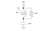
- the gate pad 22 A termination circuit 60 is connected to the end away from the connection position.
- the termination circuit 60 shown in FIG. 3 includes a coil 601 and a capacitor (DC block capacitor) 602.
- FIG. 2 shows a case where the termination circuit 60 shown in FIG. 3 is used.
- the coil 601 has a connection terminal 603 connected to the gate finger 20 side (the end of the gate finger 20 in the example of FIG. 2) at one end.
- the coil 601 has a function of making the impedance of the termination circuit 60 inductive at the signal frequency using the inductance of the coil 601 itself.
- the capacitor 602 has one end connected in series to the other end opposite to the connection terminal 603 side of the coil 601 and the other end grounded.
- the capacitor 602 mainly functions so that a bias DC voltage applied to the gate is not short-circuited. Note that the arrangement is not limited to that shown in FIG. 3, and the arrangement of the coil 601 and the capacitor 602 may be reversed.
- FIG. 4 an analysis result example of the maximum gain (hereinafter, MAGMSG) that can be stably realized by the FET is shown in FIG.
- the termination circuit 60 shown in FIG. 3 was used.
- the solid line indicates the frequency characteristics of the FET according to the first embodiment
- the broken line indicates the frequency characteristics of the conventional FET.
- FIG. 4 it can be seen that the gain that has been reduced in the high-frequency region (about 30 GHz or more) in the conventional FET is improved in the FET according to the first embodiment.
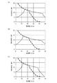
- FIG. 5 shows an analysis result example of the voltage distribution in one gate finger 20 in the conventional FET.
- the analysis of FIG. 5 shows a case where an FET having a gate length of 0.25 ⁇ m and a gate width (Wgu) of 100 ⁇ m is formed on GaN on the SiC substrate, and the analysis frequency is 30 GHz.
- the solid line is the normalized voltage amplitude distribution
- the broken line is the normalized voltage phase distribution.
- the fluctuation of the voltage amplitude in the gate finger 20 is about 0.5
- the fluctuation of the voltage phase is about 40 °.
- FIG. 6 shows an example of the analysis result of the voltage distribution in one gate finger 20 in the FET according to the first embodiment.
- the termination circuit 60 shown in FIG. 3 is used, and the capacitor 602 having an infinite capacitance and the coil 601 having an inductance of 0.3 nH are used.
- the solid line is the normalized voltage amplitude distribution
- the broken line is the normalized voltage phase distribution.
- the fluctuation of the voltage amplitude in the gate finger 20 is about 0.2
- the fluctuation of the voltage phase is about 10 °. That is, the voltage distribution in the gate finger 20 is uniform as compared with the analysis result example in the conventional FET shown in FIG. As one of the effects, an improvement in gain in the high frequency region shown in FIG. 4 can be obtained.
- the FET has high input admittance at high frequencies due to the influence of the gate-source capacitance of the FET itself.
- an impedance matching ratio is high in an FET with high input admittance, which adversely affects the frequency range in which the amplifier exhibits good characteristics.
- FIG. 7 shows an example of calculation results of input admittance in the FET according to the first embodiment.
- the alternate long and short dash line is the input admittance (0.053S) in the conventional FET
- the solid line is an example of the calculation result of the input admittance in the FET according to the first embodiment
- the horizontal axis is the coil in the termination circuit 60.
- 601 is the inductance.
- the input admittance of the FET of the first embodiment can be reduced as compared with the conventional FET.
- the area efficiency can be improved by selecting a coil 601 having a value higher than the inductance that minimizes the input admittance.
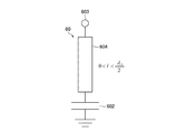
- a termination circuit 60 shown in FIG. 8 is obtained by replacing the coil 601 used to realize the inductive load in FIG. 3 with a transmission line 604.
- the transmission line 604 has a connection terminal 603 connected to the gate finger 20 side at one end, and the line length l is configured to have a length equal to or less than a half wavelength at the signal frequency (0 ⁇ l ⁇ g / 2). It is. Note that one end of the capacitor 602 is connected in series to the other end of the transmission line 604.
- the line length l of the transmission line 604 is designed based on the transmission line theory. That is, when a capacitor 602 having a capacitance C is connected to the end of a low-loss transmission line 604 having a line length l, the imaginary part Im ⁇ Z in ⁇ of the input impedance is expressed by the following equation (1).
- Z 0 is a characteristic impedance
- ⁇ is an angular frequency
- ⁇ is a phase constant.
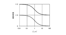
- FIG. 9 shows the relationship between the normalized imaginary part of the impedance and the line wavelength of the transmission line 604 in the termination circuit 60 shown in FIG.
- the two-dot chain line has a capacity.
- the range in which the imaginary part of the input impedance is positive varies depending on the capacitance of the capacitor 602.
- FIG. 10 shows the result of obtaining the lower limit and upper limit of the line wavelength of the transmission line 604 in which the imaginary part of the input impedance is positive with respect to Z 0 ⁇ C.
- the lower limit of the line wavelength is indicated by a broken line
- the upper limit is indicated by a solid line.
- the range of the line length l is 0 ⁇ l ⁇ g / 2.
- a circuit in which a transmission line 604 having a line length of half a wavelength or less is connected to the capacitor 602 operates in the same manner as in FIG. 3 by appropriately selecting the capacitance and the line length. Thereby, the inductive impedance of the termination circuit 60 can be realized. Note that the arrangement is not limited to the arrangement shown in FIG. 8, and the arrangement of the transmission line 604 and the capacitor 602 may be reversed.
- the termination circuit 60 shown in FIG. 11 is composed of a transmission line 605.
- the transmission line 605 has a connection terminal 603 connected to the gate finger 20 side at one end, the other end is opened, and the line length l is a length ( ⁇ or more than a quarter wavelength and a half wavelength or less of the signal frequency). g / 2 ⁇ l ⁇ g / 4). Also with this configuration, the inductive impedance of the termination circuit 60 can be realized.
- a termination circuit 60 shown in FIG. 12 is obtained by adding a resistor 606 and a gate bias terminal 607 to the configuration shown in FIG.
- the resistor 606 has one end connected to a connection point between the coil 601 and the capacitor 602.
- the gate bias terminal 607 is connected to the other end of the resistor 606 and supplies a gate bias.
- the termination circuit 60 shown in FIG. 13 is obtained by adding a resistor (second resistor) 608 to the configuration shown in FIG.
- the resistor 608 is connected in series to the main circuit portion of the termination circuit 60. In FIG. 13, it is inserted between the coil 601 and the capacitor 602.
- the termination circuit 60 shown in FIG. 13 has a configuration in which a part of the input power of the signal frequency is consumed by the resistor 608, and the high frequency characteristics are lower than that of the termination circuit 60 shown in FIGS.
- the termination circuit 60 shown in FIG. 13 by providing the termination circuit 60 shown in FIG. 13, the distribution of the gate voltage is reduced, so that the high frequency characteristics are improved.
- FIG. 14 shows the result of analysis using the capacitor 602 of the termination circuit 60 shown in FIG. 13 as infinite and the resistance 608 (R) and the inductance L of the coil 601 as variables.
- FIG. 14A is a diagram showing the contour of the non-uniformity of the gate voltage in the FET.
- FIG. 14B shows a contour line obtained by analyzing MAGMSG.
- the non-uniformity of the gate voltage shown in FIG. 14A is a value obtained by normalizing the standard deviation of the gate voltage with the average value of the gate voltage.
- the non-uniformity of the gate voltage is desirably small, and is an evaluation value that is 0 in an ideal state.
- a broken line in FIG. 14 indicates a real part of the characteristic impedance in the gate finger 20.
- the limit value of the non-uniformity of the gate voltage is 0.104, and MAGMSG is 10.88 dB.
- the non-uniformity of the gate voltage is 0.595 and MAGMSG is 9.15 dB.
- the nonuniformity of the gate voltage is generally small and MAGMSG is increased compared to the case where the termination circuit 60 is not connected. is made of.
- a particularly high improvement can be confirmed by setting the resistance 608 (R) of the termination circuit 60 shown in FIG. 13 to a range smaller than the real part of the characteristic impedance of the gate finger 20. Further, for MAGMSG, particularly high improvement can be confirmed by setting the resistance 608 (R) of the termination circuit 60 shown in FIG. 13 to a range smaller than the real part of the characteristic impedance of the gate finger 20.
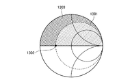
- FIG. 15 is a diagram in which the impedance range confirmed as the effect of the present invention and the impedance range where the particularly strong effect is confirmed are reflected on the Smith chart.
- the effect of the present invention is obtained when the impedance of the termination circuit 60 is in the upper half of the Smith chart including the real axis (ranges 1301 and 1303 in FIG. 15).
- Particularly effective is the range 1303 in which the impedance of the termination circuit 60 is equal to or less than the real part 1302 of the characteristic impedance of the gate finger 20.
- the characteristic impedance of the gate finger 20 is expressed by the following equation (1) using the Y parameter component (1, 1) y 11 per unit gate width of the true part of the FET and the impedance Z Fin per unit gate width of the gate finger 20. ). ⁇ (Z Fin ⁇ y 11 ) (1)
- FIG. 16 shows the result of analyzing the stability (K value) at 1 MHz, which is considered to be sufficiently lower than the signal frequency.
- the resistance 608 of the termination circuit 60 shown in FIG. 13 is 10 ⁇ , and the capacitance of the capacitor 602 of the termination circuit 60 is on the horizontal axis.
- the stability is increased by applying the present invention.
- the capacitance of the capacitor 602 for obtaining the same stability can be realized low, and the space for realizing the capacitance of the capacitor 602 can be reduced.
- the capacitance of the capacitor 602 for obtaining the same stability can be reduced to about 1/3 by applying the present invention.
- the effect of the present invention can be similarly obtained when a semiconductor junction capacitor is used for the capacitor 602 of the termination circuit 60.
- a semiconductor junction capacitance is used, a necessary capacitance can be obtained in the process of manufacturing the FET, and thus an effect of simplifying the production can be obtained.
- an inductive impedance is obtained at the frequency of the signal input from the input terminal 21a of the gate finger 20, and from the connection position of the input terminal 21a of the gate finger 20. Since the termination circuit 60 connected to the remote end is provided, the voltage in one cell of the FET can be equalized.
- FIG. 13 shows the case where the resistor 608 is inserted between the coil 601 and the capacitor 602 shown in FIG. 3, the present invention is not limited to this. Anything is acceptable.
- a resistor 608 may be connected in series to the main circuit portion of the termination circuit 60 shown in FIGS. 8 and 12 or the termination circuit 60 shown in FIG.
- the connection location of the resistor 608 in the main circuit portion may be any location, and does not need to be between the coil 601 and the capacitor 602 as shown in FIG.
- FIG. 17 is a view showing a structure pattern of an FET according to the second embodiment of the present invention.
- a plurality of gate fingers 20 are arranged in parallel in the active region on the semiconductor substrate 1, and a plurality of source fingers 30 and a plurality of drain fingers 40 are alternately sandwiched between the gate fingers 20. They are arranged in parallel.
- the grounding of the source finger 30 is not shown for simplification.
- all the gate fingers 20 are bundled at one end by a gate bus 23 and connected to a gate pad 22 (corresponding to the input terminal 21a shown in FIG. 1).
- the gate finger 20 is electrically connected to the signal source 50 (not shown in FIG. 17) via the gate pad 22.
- All the drain fingers 40 are bundled at one end by a drain bus 44 (corresponding to the connection terminal 41b shown in FIG. 1) via a drain air bridge 43.
- the drain finger 40 is electrically connected to an external circuit via the drain bus 44.
- all the gate fingers 20 are connected by a connection line 24 passing under the drain air bridge 43 in a region opposite to the region where the gate pad 22 is disposed with the active region interposed therebetween.
- a termination circuit 60 is connected to the connection line 24. At this time, it is desirable to connect the termination circuit 60 at a position farthest from the connection position of the gate pad 22 in the connection line 24.
- the termination circuit 60 shown in FIG. 17 is an example of the circuit shown in FIG. 3 in which a coil 601 and a capacitor 602 are connected in series, which is the simplest of the termination circuits 60 shown in the first embodiment.
- the termination circuit 60 in the second embodiment is not limited to the configuration shown in FIG. 3, and may be any circuit that has an inductive impedance at the signal frequency, and may be the termination circuit 60 shown in FIGS. .
- the characteristic impedance of the gate finger 20 is approximately inversely proportional to the number of parallels compared to the case of the single finger transistor.
- the gate finger 20 is terminated with an inductive impedance by using the termination circuit 60.
- the voltage distribution can be improved and the high frequency characteristics can be improved.
- the configuration shown in FIG. 17 can also improve the voltage distribution between the gate fingers 20.
- a voltage is also distributed in the inter-finger direction shown in FIG.
- the voltage distribution between the gate fingers 20 is affected by a phase difference generated between the gate fingers 20.
- the phase difference between the gate fingers 20 in the multi-finger transistor can be obtained by the following equation (2). Im ⁇ cosh ⁇ 1 (1- ( ⁇ 11 ⁇ Z BUS / 2)) ⁇ (2)
- ⁇ 11 is an input admittance of one finger transistor
- Z BUS is an impedance parasitic between the gate fingers 20 in the gate bus 23.
- the FET shown in FIG. 17 is effective for both the improvement of the uniformity of the voltage distribution in the gate finger 20 and the improvement of the uniformity of the voltage distribution between the gate fingers 20, and the high frequency characteristics of the FET. Can be improved.
- FIG. 18 shows an example of the analysis result of the voltage distribution in one gate finger 20 in the FET according to the second embodiment.
- an 8-finger multi-finger transistor is used.
- the inductance of the coil 601 of the termination circuit 60 shown in FIG. 3 is 0.027 nH
- the capacitance of the capacitor 602 is infinite
- the voltage at the connection position with the gate finger 20 was analyzed.
- 18A shows the standardized voltage amplitude in the gate bus 23
- FIG. 18B shows the standardized voltage phase in the gate bus 23.
- the solid line is the analysis result of the FET according to the second embodiment
- the broken line is the analysis result of the conventional FET.
- the voltage amplitude has a voltage amplitude deviation of about 0.6 in the case of the conventional FET, but the voltage amplitude deviation of about 0.2 in the FET according to the second embodiment.
- the voltage phase is about 30 ° in the FET according to the second embodiment, whereas the conventional FET has a voltage phase deviation of about 80 °. The improvement of the voltage deviation improves the high frequency characteristics of the multi-finger transistor.
- FIG. 17 shows a case where all the gate fingers 20 are connected and the termination circuit 60 having inductive impedance is connected to a position farthest from the gate pad 22 of the connection line 24.
- the present invention is not limited to this, and a termination circuit 60 may be provided for each gate finger 20, and each termination circuit 60 may be connected to a connection position of the corresponding gate finger 20 on the connection line 24, thereby obtaining the same effect. Can do. Actually, there are often cases where the termination circuit 60 cannot be arranged for each gate finger 20 due to restrictions on the circuit size. In that case, several termination circuits 60 are combined into one.
- FIG. 17 shows a case where all the gate fingers 20 are connected and the termination circuit 60 having inductive impedance is connected to the position farthest from the gate pad 22 of the connection line 24.
- the present invention is not limited to this, and a similar effect can be obtained when the connection line 24 is connected to a position closest to the gate pad 22.
- FIG. 19 shows an analysis result example of the high-frequency characteristics of MAGMSG when the connection method and connection position of termination circuit 60 in the second embodiment are changed.
- FIG. 19A shows a case where the termination circuit 60 is connected to each gate finger 20
- FIG. 19B shows a case where the termination circuit 60 is connected at a position farthest from the gate pad 22 of the connection line 24
- FIG. 19C shows a case where the termination circuit 60 is connected to a position of the connection line 24 closest to the gate pad 22.
- the solid line is an example of the analysis result of the FET according to the second embodiment
- the broken line is an example of the analysis result of the conventional FET. In this case, when the termination circuit 60 is connected to each gate finger 20 shown in FIG.
- FIG. 21 shows an example of a MAGMSG analysis result when the inductance of the coil 601 of the termination circuit 60 is 0.04 nH and the capacitance of the capacitor 602 is infinite.
- the solid line is an example of the analysis result in the FET shown in FIG. 20
- the broken line is an example of the analysis result in the conventional FET.
- FIG. 22 shows a particularly effective configuration example of the termination circuit 60 used for the multi-finger transistor.
- a feedback loop is formed in the FET at an extremely high frequency (millimeter wave band or the like), and oscillation may occur.
- this oscillation frequency is higher than the signal frequency, it is effective to use a termination circuit 60 shown in FIG.
- the termination circuit 60 shown in FIG. 22 is obtained by adding a resistor 609 connected in parallel to the coil 601 to the configuration shown in FIG.
- the termination circuit 60 shown in FIG. 22 has an inductive input impedance due to the inductance of the coil 601 at the signal frequency. At a higher frequency, the impedance of the coil 601 becomes high, and the resistor 606 connected in parallel becomes dominant and causes a large loss. Therefore, in the termination circuit 60 shown in FIG. 22, the loss increases as the frequency increases, and there is an effect of reducing unnecessary high frequency gain. This reduces the risk of oscillation.
- the circuit in which the resistor 608 is inserted in series with the circuit shown in FIG. 22 has the effect of improving the stability in the low frequency region as described in the first embodiment. Note that the termination circuit 60 shown in FIG. 22 is also applicable to a single finger transistor.
- the multi-finger transistor in the multi-finger transistor, is provided in the region opposite to the region where the gate bus 23 is provided across the active region, and the other end side of the gate finger 20 is connected to the multi-finger transistor. Even if the connection line 24 to be connected and the termination circuit 60 connected to the connection line 24 have an inductive impedance at the frequency of the signal input from the input terminal 21a connected to the gate bus 23, one cell of the FET is provided. The internal voltage can be made uniform.
- FIG. FIG. 23 is a view showing the structure pattern of the FET according to the third embodiment of the present invention.
- the FET according to the third embodiment shown in FIG. 23 is obtained by removing the connection line 24 from the FET according to the second embodiment shown in FIG. 17 and changing the connection position of the termination circuit 60. Further, the drain air bridge 43 is not necessary, and each drain finger 40 is directly connected to the drain bus 44. Other configurations are the same, and only the different parts are described with the same reference numerals.
- the termination circuit 60 is connected to the gate bus 23 of the multi-finger transistor. At this time, it is desirable to connect the termination circuit 60 at a position farthest from the connection position of the gate pad 22 of the gate bus 23.
- the voltage distribution generated between the gate fingers 20 can be changed by changing the boundary condition at both ends of the gate bus 23 at positions away from the feeding point, which is the connection position of the gate pad 22. Analysis has shown that it is the inductive impedance that improves the voltage distribution between the gate fingers 20.
- FIG. 24 shows an example of the analysis result of the voltage distribution in one gate finger 20 in the FET according to the third embodiment.
- the inductance of the coil 601 of the termination circuit 60 shown in FIG. 22 is 0.063 nH
- the capacitance of the capacitor 602 is infinite
- the voltage at the connection position of each gate finger 20 of the gate bus 23 is analyzed.
- . 24A shows the standardized voltage amplitude in the gate bus 23
- FIG. 24B shows the standardized voltage phase in the gate bus 23.
- FIG. 24 (a) and 24 (b) the solid line is the analysis result of the FET according to the third embodiment, and the broken line is the analysis result of the conventional FET. As shown in FIG.
- the voltage amplitude has a voltage amplitude deviation of about 0.6 in the case of the conventional FET, but the voltage amplitude deviation of about 0.3 in the FET according to the third embodiment.
- the voltage phase is about 50 ° in the FET according to the third embodiment, while the voltage phase deviation of the conventional FET is about 80 °.
- the improvement of the voltage deviation improves the high frequency characteristics of the multi-finger transistor. The frequency characteristics at this time are shown in FIG. From FIG. 25, it can be seen that the high-frequency characteristics are improved slightly.
- the solid line is an example of the analysis result of the FET according to the third embodiment
- the broken line is an example of the analysis result of the conventional FET.
- an inductive impedance is obtained at the frequency of the signal input from the input terminal 21a connected to the gate bus 23, and the multi-finger transistor is connected to the gate bus 23. Even if the termination circuit 60 is provided, the voltage in one cell of the FET can be made uniform.
- FIG. 26 is a view showing a structure pattern of an FET according to the fourth embodiment of the present invention.
- the FET according to the fourth embodiment shown in FIG. 26 is provided with the termination circuit 60 of the FET according to the third embodiment shown in FIG. 23 for each gate finger 20.
- Other configurations are the same, and only the different parts are described with the same reference numerals.
- each termination circuit 60 is connected to the connection position of the corresponding gate finger 20 on the gate bus 23. .
- the input admittance of the termination circuit 60 is preferably selected so that the imaginary part at the signal frequency is opposite in sign to the imaginary part of the input admittance of one finger transistor and has the same absolute value. As described above, it is effective to reduce the input admittance of one finger transistor in order to reduce the phase difference between fingers from the equation (2). Then, as a method of lowering the input admittance of one finger transistor equivalently, a circuit having an imaginary part of an input admittance that is different in sign from the imaginary part of the input admittance of the one finger transistor and has the same absolute value is connected in parallel. As a result, the imaginary parts of the input admittance of the loaded circuit and the loaded circuit cancel each other, and low admittance can be realized.
- termination circuit 60 cannot be arranged for each gate finger 20 due to restrictions on the circuit size. In that case, several termination circuits 60 are combined into one.
- the input admittance of the termination circuit 60 can be reduced.
- FIG. FIG. 27 is a view showing a structure pattern of an FET according to the fifth embodiment of the present invention.
- the FET according to the fifth embodiment shown in FIG. 27 is a combination of the configuration of the FET according to the second embodiment shown in FIG. 17 and the configuration of the FET according to the third embodiment shown in FIG.
- the configuration of the second embodiment shown in FIG. 17 has an effect of reducing the phase difference between the gate fingers 20.
- the configuration of the second embodiment does not completely eliminate the phase difference and voltage distribution between the gate fingers 20. Therefore, in the fifth embodiment, the voltage distribution between the gate fingers 20 that could not be solved in the second embodiment is further improved by using the configuration of the third embodiment.
- FIG. 28 shows an analysis result example of the voltage distribution in one gate finger 20 in the FET according to the fifth embodiment.
- the inductance of the coil 601 of the termination circuit 60 connected to the connection line 24 shown in FIG. 27 is 0.027 nH
- the inductance of the coil 601 of the termination circuit 60 connected to the gate bus 23 is 0.316 nH
- the capacitance of the capacitor 602 of both the termination circuits 60 was set to infinity
- the voltage at the connection position of each gate finger 20 of the gate bus 23 was analyzed.
- FIG. 28A shows the normalized voltage amplitude in the gate bus 23
- FIG. 28B shows the normalized voltage phase in the gate bus 23.
- the solid line represents the analysis result of the FET according to the fifth embodiment
- the broken line represents the analysis result of the conventional FET.
- the voltage amplitude has a voltage amplitude deviation of about 0.6 in the case of the conventional FET, but the voltage amplitude deviation of about 0.1 in the FET according to the fifth embodiment.
- the conventional FET has a voltage phase deviation of about 80 °
- the FET according to the fifth embodiment has a voltage phase of about 20 °.
- the improvement of the voltage deviation improves the high frequency characteristics of the multi-finger transistor.
- the voltage distribution between the gate fingers 20 can be further improved as compared with the second embodiment. it can.
- the semiconductor device according to the present invention can equalize the voltage in one cell of the semiconductor device and is suitable for use in a semiconductor device such as a field effect transistor used in a high frequency power amplifier.
Abstract
Description
実施の形態1.
図1はこの発明の実施の形態1に係るFETの構成を示す斜視図である。なお以下では、半導体装置として、高周波電力増幅器に用いられるFETを例に説明を行うが、これに限るものではない。
図3に示す終端回路60は、コイル601及びコンデンサ(DCブロック用コンデンサ)602から構成されている。図2では、図3に示す終端回路60を用いた場合を示している。
コンデンサ602は、一端がコイル601の接続端子603側とは反対側である他端に直列接続され、他端が接地されたものである。このコンデンサ602は、主として、ゲートに加えるバイアス直流電圧が短絡されないよう機能する。
なお図3に示す配置に限るものではなく、コイル601とコンデンサ602の配置を反対にしてもよい。
この図4に示すように、従来のFETにおいて高周波領域(約30GHz以上)で低下していた利得が、実施の形態1に係るFETでは改善していることがわかる。
この図5に示すように、従来のFETでは、ゲートフィンガ20内での電圧振幅の変動が約0.5となり、電圧位相の変動が約40°となっている。
この図6に示すように、実施の形態1に係るFETでは、ゲートフィンガ20内での電圧振幅の変動が約0.2となり、電圧位相の変動が約10°となっている。すなわち、図5に示す従来のFETでの解析結果例と比較して、ゲートフィンガ20内の電圧分布が一様になっている。そして、その一つの効果として、図4に示した高周波領域での利得の改善が得られる。
FETは、高周波において、FET自身が有するゲート-ソース間容量の影響によって入力アドミタンスが高くなる。FETを増幅器として用いる場合、入力アドミタンスが高いFETではインピーダンス整合比が高くなり、増幅器が良好な特性を示す周波数範囲に悪影響を及ぼす。
この図7に示すように、実施の形態1のFETでは、従来のFETに対して、入力アドミタンスを低下できることがわかる。また、実施の形態1のFETでは、入力アドミタンスを最も下げることができるインダクタンスが存在する。そして、コイル601として、この入力アドミタンスを最低とするインダクタンスより高い値のものを選定することで、面積効率を向上させることができる。
図8に示す終端回路60は、図3において誘導性負荷を実現するために用いたコイル601を、伝送線路604に置き換えたものである。
伝送線路604は、一端にゲートフィンガ20側に接続される接続端子603を有し、線路長lが信号周波数における半波長以下の長さ(0<l<λg/2)に構成されたものである。
なお、コンデンサ602は、一端が伝送線路604の他端に直列接続されている。
すなわち、線路長lの低損失な伝送線路604の終端に容量Cのコンデンサ602が接続された場合、入力インピーダンスの虚部Im{Zin}は下式(1)で表される。


この図9に示すように、コンデンサ602の容量によって、入力インピーダンスの虚部が正となる範囲が変動する。
この図10に示すように、使用するコンデンサ602の容量が決定していない状態では、線路長lの範囲は0<l<λg/2となる。
なお図8に示す配置に限るものではなく、伝送線路604とコンデンサ602の配置を反対にしてもよい。
伝送線路605は、一端にゲートフィンガ20側に接続される接続端子603を有し、他端が開放され、線路長lが信号周波数における四分の一波長以上且つ半波長以下の長さ(λg/2<l<λg/4)に構成されたものである。この構成によっても、終端回路60の誘導性インピーダンスを実現することができる。
抵抗606は、一端がコイル601とコンデンサ602との接続点に接続されたものである。また、ゲートバイアス端子607は、抵抗606の他端に接続され、ゲートバイアスを供給するものである。
図12に示す終端回路60を用いることで、FETでの低周波領域における発振に対して安定性が改善される。
抵抗608は、終端回路60の主回路部分に直列接続されたものである。図13では、コイル601とコンデンサ602との間に挿入されている。
図13に示す終端回路60は、信号周波数の入力電力の一部を抵抗608で消費する構成であり、図3,8,11,12に示す終端回路60より高周波特性が低下する。しかしながら、従来の半導体装置のように終端回路60がない構成と比較して、図13に示す終端回路60を設けることで、ゲート電圧の分布が低減するため、高周波特性が改善される。
なお、図14(a)に示すゲート電圧の不均一性とは、ゲート電圧の標準偏差をゲート電圧の平均値で規格化した値である。このゲート電圧の不均一性は、小さいことが望ましく、理想状態で0となる評価値である。なお、R=0の極限が、図3に示す終端回路60と同値となる条件である。また、図14上の破線は、ゲートフィンガ20における特性インピーダンスの実部を示している。
これに対して、図13に示す構成では、抵抗608が0ではない場合も、終端回路60を接続しない場合と比較して、概ね、ゲート電圧の不均一性が少なく、MAGMSGを高くすることができている。
この図15に示すように、終端回路60のインピーダンスが、実軸を含むスミスチャートの上半分(図15の範囲1301,1303)にあるときに本願発明の効果がある。また、特に効果が高いのは、終端回路60のインピーダンスが、ゲートフィンガ20における特性インピーダンスの実部1302以下となる範囲1303である。上記ゲートフィンガ20における特性インピーダンスは、FETの真正部の単位ゲート幅あたりのYパラメータの成分(1,1)y11とゲートフィンガ20の単位ゲート幅あたりのインピーダンスZFinを用いて下式(1)によって定義される。
√(ZFin・y11) (1)
図13に示す終端回路60を用いた場合、抵抗608が安定化の役割を果たす。
信号周波数の周辺の周波数では、入力電力を抵抗608が消費するために想像が容易であるが、極低周波の安定性が改善されることがわかっている。例として、信号周波数より十分に低いと考えられる1MHzの安定性(K値)について解析した結果を図16に示す。
この図16に示すように、同じ静電容量を用いた場合には、本願発明の適用により安定性が高くなる。別の言い方をすれば、同じ安定性を得るためのコンデンサ602の静電容量を低く実現でき、コンデンサ602の静電容量を実現するスペースを小さくできる効果がある。図16の例では、本願発明の適用により、同じ安定性を得るためのコンデンサ602の静電容量を約1/3とすることができる。
図2に示す実施の形態1では1フィンガトランジスタの場合について説明を行った。それに対し、実施の形態2ではマルチフィンガトランジスタの場合について説明を行う。図17はこの発明の実施の形態2に係るFETの構造パターンを示す図である。
ゲートフィンガ20を複数本用いるマルチフィンガトランジスタでは、実施の形態1で述べたフィンガ方向の電圧分布に加え、図17に示すフィンガ間方向にも電圧が分布する。このゲートフィンガ20間の電圧分布は、ゲートフィンガ20間に発生する位相差に影響される。マルチフィンガトランジスタにおけるゲートフィンガ20間の位相差は、下式(2)で求めることができる。
Im{cosh-1(1-(Ψ11・ZBUS/2))} (2)
ここで、Ψ11は1フィンガトランジスタの入力アドミタンスであり、ZBUSはゲートバス23におけるゲートフィンガ20間に寄生するインピーダンスである。
したがって、図17に示すFETでは、ゲートフィンガ20内の電圧分布の均一性の改善と、ゲートフィンガ20間の電圧分布の均一性の改善との両方に対して効果を発揮し、FETの高周波特性を改善することができる。
また、図18では、ゲートフィンガ20をx=Wguで連結し、図3に示す終端回路60のコイル601のインダクタンスを0.027nH、コンデンサ602の静電容量を無限大とし、ゲートバス23の各ゲートフィンガ20との接続位置における電圧を解析した。図18(a)はゲートバス23における規格化した電圧振幅であり、図18(b)はゲートバス23における規格化した電圧位相である。図18(a),(b)において、実線は実施の形態2に係るFETの解析結果であり、破線は従来のFETの解析結果である。
図18に示すように、電圧振幅については、従来のFETの場合では約0.6の電圧振幅偏差があるが、実施の形態2に係るFETでは約0.2の電圧振幅偏差である。また、電圧位相についても、従来のFETでは約80°の電圧位相偏差があるのに対して、実施の形態2に係るFETでは約30°程度となっている。この電圧偏差の改善によりマルチフィンガトランジスタの高周波特性が改善される。
なお、現実的には、回路サイズの制約上等で、ゲートフィンガ20毎に終端回路60が配置できない場合がしばしばある。その場合には、数個の終端回路60をまとめて一つにする。
この場合、図19(a)に示すゲートフィンガ20毎に終端回路60を接続した場合が、最も高周波まで高い利得が実現できている。そして、図19(b)に示す連結線路24のゲートパッド22から最も離れた位置に終端回路60を接続した場合が、二番目に高周波特性が改善できている。そして、図19(c)に示す連結線路24のゲートパッド22に最も近い位置に終端回路60を接続した場合が、高周波特性を改善する量が最も少ない。すなわち、図19(c)の構成では、連結線路24内にも電圧分布が生じてしまう。そのため、上記のような終端回路60の接続方法及び接続位置の違いによって優位性が生じる。
この図21に示すように、図20に示す構成においても、高周波特性が大きく改善していることがわかる。
マルチフィンガトランジスタでは、極めて高い周波数(ミリ波帯等)においてFET内で帰還ループができてしまい、発振することがある。この発振周波数が信号周波数よりも高いときには、図22に示す終端回路60を用いることが有効である。
なお、図22に示す終端回路60は、1フィンガトランジスタにも適用可能である。
図23はこの発明の実施の形態3に係るFETの構造パターンを示す図である。この図23に示す実施の形態3に係るFETは、図17に示す実施の形態2に係るFETから連結線路24を取除き、終端回路60の接続位置を変更したものである。また、ドレインエアブリッジ43も不要であり、各ドレインフィンガ40はドレインバス44に直接接続されている。その他の構成は同様であり、同一の符号を付して異なる部分についてのみ説明を行う。
この図24に示すように、電圧振幅については、従来のFETの場合では約0.6の電圧振幅偏差があるが、実施の形態3に係るFETでは約0.3の電圧振幅偏差である。また、電圧位相についても、従来のFETでは約80°の電圧位相偏差があるのに対して、実施の形態3に係るFETでは約50°程度となっている。この電圧偏差の改善によりマルチフィンガトランジスタの高周波特性が改善される。また、このときの周波数特性を図25に示す。この図25から、わずかではあるが、高周波特性が改善していることがわかる。なお図25において、実線は実施の形態3に係るFETの解析結果例であり、破線は従来のFETの解析結果例である。
図26はこの発明の実施の形態4に係るFETの構造パターンを示す図である。この図26に示す実施の形態4に係るFETは、図23に示す実施の形態3に係るFETの終端回路60をゲートフィンガ20毎に設けたものである。その他の構成は同様であり、同一の符号を付して異なる部分についてのみ説明を行う。
そして、1フィンガトランジスタの入力アドミタンスを等価的に下げる方法として、1フィンガトランジスタの入力アドミタンスの虚部と符号が異なり且つ絶対値が等しい入力アドミタンスの虚部を有する回路を並列に接続する。これにより、1フィンガトランジスタと負荷した回路の入力アドミタンスの虚部が互いに打ち消し合い、低いアドミタンスを実現できる。
図27はこの発明の実施の形態5に係るFETの構造パターンを示す図である。図27に示す実施の形態5に係るFETは、図17に示す実施の形態2に係るFETの構成と、図23に示す実施の形態3に係るFETの構成とを組み合わせたものである。
この図28に示すように、電圧振幅については、従来のFETの場合では約0.6の電圧振幅偏差があるが、実施の形態5に係るFETでは約0.1の電圧振幅偏差である。電圧位相についても、従来のFETでは約80°の電圧位相偏差があるのに対して、実施の形態5に係るFETでは約20°程度となっている。この電圧偏差の改善によりマルチフィンガトランジスタの高周波特性が改善される。
Claims (11)
- 半導体基板上の活性領域に設けられた一本以上のゲートフィンガと、前記活性領域に設けられ、前記ゲートフィンガを挟んで交互に配置されたソースフィンガ及びドレインフィンガとを備えた半導体装置において、
前記ゲートフィンガの入力端子から入力される信号の周波数において誘導性インピーダンスとなり、当該ゲートフィンガの当該入力端子の接続位置から離れた箇所で当該ゲートフィンガに直接又は間接的に接続された終端回路を備えた
ことを特徴とする半導体装置。 - 前記ゲートフィンガ、前記ソースフィンガ及び前記ドレインフィンガはそれぞれ一本ずつ設けられ、
前記終端回路は前記ゲートフィンガに直接接続された
ことを特徴とする請求項1記載の半導体装置。 - 前記ゲートフィンガ、前記ソースフィンガ及び前記ドレインフィンガはそれぞれ複数本ずつ設けられ、
全ての前記ゲートフィンガの一端側を束ねるゲートバスと、
前記活性領域を挟んで前記ゲートバスが設けられた領域とは反対側の領域に設けられ、前記ゲートフィンガの他端側を連結する連結線路とを備え、
前記終端回路は前記連結線路に接続された
ことを特徴とする請求項1記載の半導体装置。 - 前記ゲートフィンガ、前記ソースフィンガ及び前記ドレインフィンガはそれぞれ複数本ずつ設けられ、
全ての前記ゲートフィンガの一端側を束ねるゲートバスを備え、
前記終端回路は前記ゲートバスに接続された
ことを特徴とする請求項1記載の半導体装置。 - 前記終端回路は、前記ゲートバスにも接続された
ことを特徴とする請求項3記載の半導体装置。 - 前記終端回路は、前記入力端子の接続位置から最も離れた位置に接続された
ことを特徴とする請求項3記載の半導体装置。 - 前記終端回路は、前記入力端子の接続位置から最も離れた位置に接続された
ことを特徴とする請求項4記載の半導体装置。 - 前記終端回路は複数設けられた
ことを特徴とする請求項3記載の半導体装置。 - 前記終端回路は複数設けられた
ことを特徴とする請求項4記載の半導体装置。 - 前記終端回路は、
線路長が前記入力端子から入力される信号の周波数における半波長以下の長さである伝送線路と、
前記伝送線路に直列接続されたコンデンサとを有し、
前記終端回路の端部が接地された
ことを特徴とする請求項1記載の半導体装置。 - 前記終端回路は、
端部が開放され、線路長が前記入力端子から入力される信号の周波数における四分の一波長以上且つ半波長以下の長さである伝送線路を有する
ことを特徴とする請求項1記載の半導体装置。
Priority Applications (5)
| Application Number | Priority Date | Filing Date | Title |
|---|---|---|---|
| CN201580075517.XA CN107210228B (zh) | 2015-02-04 | 2015-06-23 | 半导体装置 |
| EP15881140.6A EP3255655A4 (en) | 2015-02-04 | 2015-06-23 | Semiconductor device |
| KR1020177021735A KR101882638B1 (ko) | 2015-02-04 | 2015-06-23 | 반도체 장치 |
| US15/545,373 US10355130B2 (en) | 2015-02-04 | 2015-06-23 | Semiconductor device |
| JP2015558048A JP5989264B1 (ja) | 2015-02-04 | 2015-06-23 | 半導体装置 |
Applications Claiming Priority (2)
| Application Number | Priority Date | Filing Date | Title |
|---|---|---|---|
| JP2015020221 | 2015-02-04 | ||
| JP2015-020221 | 2015-02-04 |
Publications (1)
| Publication Number | Publication Date |
|---|---|
| WO2016125323A1 true WO2016125323A1 (ja) | 2016-08-11 |
Family
ID=56563683
Family Applications (1)
| Application Number | Title | Priority Date | Filing Date |
|---|---|---|---|
| PCT/JP2015/068033 WO2016125323A1 (ja) | 2015-02-04 | 2015-06-23 | 半導体装置 |
Country Status (6)
| Country | Link |
|---|---|
| US (1) | US10355130B2 (ja) |
| EP (1) | EP3255655A4 (ja) |
| JP (1) | JP5989264B1 (ja) |
| KR (1) | KR101882638B1 (ja) |
| CN (1) | CN107210228B (ja) |
| WO (1) | WO2016125323A1 (ja) |
Cited By (2)
| Publication number | Priority date | Publication date | Assignee | Title |
|---|---|---|---|---|
| WO2019229982A1 (ja) * | 2018-06-01 | 2019-12-05 | 三菱電機株式会社 | 半導体装置 |
| WO2022102137A1 (ja) * | 2020-11-16 | 2022-05-19 | 三菱電機株式会社 | トランジスタ |
Families Citing this family (4)
| Publication number | Priority date | Publication date | Assignee | Title |
|---|---|---|---|---|
| US11255357B2 (en) | 2018-06-12 | 2022-02-22 | Kosmek Ltd. | Cylinder |
| US10629526B1 (en) * | 2018-10-11 | 2020-04-21 | Nxp Usa, Inc. | Transistor with non-circular via connections in two orientations |
| US10855244B2 (en) * | 2018-10-19 | 2020-12-01 | Cree, Inc. | Transistor level input and output harmonic terminations |
| CN114078863A (zh) * | 2020-10-29 | 2022-02-22 | 长江存储科技有限责任公司 | 半导体器件、三维存储器及半导体器件制备方法 |
Citations (2)
| Publication number | Priority date | Publication date | Assignee | Title |
|---|---|---|---|---|
| JPH01200809A (ja) * | 1987-12-18 | 1989-08-14 | Philips Gloeilampenfab:Nv | 少なくとも負荷電界効果トランジスタを具える高周波回路 |
| JPH0432309A (ja) * | 1990-05-29 | 1992-02-04 | Fujitsu Ltd | 半導体装置 |
Family Cites Families (10)
| Publication number | Priority date | Publication date | Assignee | Title |
|---|---|---|---|---|
| JP2643662B2 (ja) | 1991-07-08 | 1997-08-20 | 三菱電機株式会社 | 高出力電界効果トランジスタ増幅器 |
| US5519358A (en) * | 1994-08-15 | 1996-05-21 | Texas Instruments Incorporated | Reactively compensated power transistors |
| JP2739851B2 (ja) | 1995-10-13 | 1998-04-15 | 日本電気株式会社 | マイクロ波トランジスタ |
| WO2010113779A1 (ja) | 2009-03-30 | 2010-10-07 | 日本電気株式会社 | 半導体装置 |
| US8212321B2 (en) * | 2009-10-30 | 2012-07-03 | Freescale Semiconductor, Inc. | Semiconductor device with feedback control |
| JP2013042193A (ja) | 2009-12-03 | 2013-02-28 | Panasonic Corp | スイッチ装置 |
| JP5529607B2 (ja) * | 2010-03-29 | 2014-06-25 | セイコーインスツル株式会社 | 半導体装置 |
| JP5733616B2 (ja) * | 2011-04-21 | 2015-06-10 | 住友電工デバイス・イノベーション株式会社 | 半導体装置 |
| WO2012160755A1 (ja) | 2011-05-24 | 2012-11-29 | パナソニック株式会社 | 高周波増幅回路 |
| JP6136165B2 (ja) * | 2012-09-28 | 2017-05-31 | 住友電気工業株式会社 | 電子回路 |
-
2015
- 2015-06-23 CN CN201580075517.XA patent/CN107210228B/zh active Active
- 2015-06-23 JP JP2015558048A patent/JP5989264B1/ja active Active
- 2015-06-23 US US15/545,373 patent/US10355130B2/en active Active
- 2015-06-23 WO PCT/JP2015/068033 patent/WO2016125323A1/ja active Application Filing
- 2015-06-23 KR KR1020177021735A patent/KR101882638B1/ko active IP Right Grant
- 2015-06-23 EP EP15881140.6A patent/EP3255655A4/en not_active Ceased
Patent Citations (2)
| Publication number | Priority date | Publication date | Assignee | Title |
|---|---|---|---|---|
| JPH01200809A (ja) * | 1987-12-18 | 1989-08-14 | Philips Gloeilampenfab:Nv | 少なくとも負荷電界効果トランジスタを具える高周波回路 |
| JPH0432309A (ja) * | 1990-05-29 | 1992-02-04 | Fujitsu Ltd | 半導体装置 |
Non-Patent Citations (1)
| Title |
|---|
| See also references of EP3255655A4 * |
Cited By (4)
| Publication number | Priority date | Publication date | Assignee | Title |
|---|---|---|---|---|
| WO2019229982A1 (ja) * | 2018-06-01 | 2019-12-05 | 三菱電機株式会社 | 半導体装置 |
| US11276626B2 (en) | 2018-06-01 | 2022-03-15 | Mitsubishi Electric Corporation | Semiconductor device |
| WO2022102137A1 (ja) * | 2020-11-16 | 2022-05-19 | 三菱電機株式会社 | トランジスタ |
| JP7456517B2 (ja) | 2020-11-16 | 2024-03-27 | 三菱電機株式会社 | トランジスタ |
Also Published As
| Publication number | Publication date |
|---|---|
| KR101882638B1 (ko) | 2018-07-26 |
| KR20170101304A (ko) | 2017-09-05 |
| CN107210228A (zh) | 2017-09-26 |
| EP3255655A4 (en) | 2018-10-03 |
| JPWO2016125323A1 (ja) | 2017-04-27 |
| US10355130B2 (en) | 2019-07-16 |
| US20180006152A1 (en) | 2018-01-04 |
| JP5989264B1 (ja) | 2016-09-07 |
| CN107210228B (zh) | 2020-09-29 |
| EP3255655A1 (en) | 2017-12-13 |
Similar Documents
| Publication | Publication Date | Title |
|---|---|---|
| JP5989264B1 (ja) | 半導体装置 | |
| US8384484B2 (en) | Power amplifier with improved bandwidth | |
| DE102012216840A1 (de) | HF-Bauelement mit Ausgleichsresonatoranpassungstopologie | |
| JPWO2008018338A1 (ja) | 高調波処理回路及びこれを用いた増幅回路 | |
| WO2017098578A1 (ja) | 電力増幅器 | |
| JP2015149627A (ja) | 高周波半導体増幅器 | |
| US9640530B2 (en) | Semiconductor device | |
| EP2993783B1 (en) | Semiconductor amplifier | |
| JP6837602B2 (ja) | 分布型増幅器 | |
| US9647615B2 (en) | Broadband amplifier | |
| JP6648979B2 (ja) | 半導体増幅装置 | |
| JP6943193B2 (ja) | 伝送線路、整合回路および増幅回路 | |
| JP6678827B2 (ja) | 高周波増幅器 | |
| TWI741782B (zh) | 高頻放大器 | |
| JP7444251B2 (ja) | 増幅回路 | |
| WO2021140563A1 (ja) | 高周波半導体装置 | |
| US11621680B2 (en) | Power amplifier | |
| JP5419812B2 (ja) | 高周波多段能動回路 | |
| JPH04287507A (ja) | 電界効果トランジスタ増幅器 | |
| JP6523108B2 (ja) | 高周波半導体増幅器 | |
| US20190296701A1 (en) | High frequency circuit and high frequency power amplifier | |
| JP6452315B2 (ja) | 増幅器 |
Legal Events
| Date | Code | Title | Description |
|---|---|---|---|
| ENP | Entry into the national phase |
Ref document number: 2015558048 Country of ref document: JP Kind code of ref document: A |
|
| 121 | Ep: the epo has been informed by wipo that ep was designated in this application |
Ref document number: 15881140 Country of ref document: EP Kind code of ref document: A1 |
|
| WWE | Wipo information: entry into national phase |
Ref document number: 15545373 Country of ref document: US |
|
| REEP | Request for entry into the european phase |
Ref document number: 2015881140 Country of ref document: EP |
|
| ENP | Entry into the national phase |
Ref document number: 20177021735 Country of ref document: KR Kind code of ref document: A |
|
| NENP | Non-entry into the national phase |
Ref country code: DE |