WO2016121282A1 - 高周波発振器 - Google Patents
高周波発振器 Download PDFInfo
- Publication number
- WO2016121282A1 WO2016121282A1 PCT/JP2015/086186 JP2015086186W WO2016121282A1 WO 2016121282 A1 WO2016121282 A1 WO 2016121282A1 JP 2015086186 W JP2015086186 W JP 2015086186W WO 2016121282 A1 WO2016121282 A1 WO 2016121282A1
- Authority
- WO
- WIPO (PCT)
- Prior art keywords
- negative resistance
- resistance element
- frequency oscillator
- reflecting portion
- signal
- Prior art date
- Legal status (The legal status is an assumption and is not a legal conclusion. Google has not performed a legal analysis and makes no representation as to the accuracy of the status listed.)
- Ceased
Links
Images





Classifications
-
- H—ELECTRICITY
- H03—ELECTRONIC CIRCUITRY
- H03B—GENERATION OF OSCILLATIONS, DIRECTLY OR BY FREQUENCY-CHANGING, BY CIRCUITS EMPLOYING ACTIVE ELEMENTS WHICH OPERATE IN A NON-SWITCHING MANNER; GENERATION OF NOISE BY SUCH CIRCUITS
- H03B7/00—Generation of oscillations using active element having a negative resistance between two of its electrodes
- H03B7/12—Generation of oscillations using active element having a negative resistance between two of its electrodes with frequency-determining element comprising distributed inductance and capacitance
- H03B7/14—Generation of oscillations using active element having a negative resistance between two of its electrodes with frequency-determining element comprising distributed inductance and capacitance active element being semiconductor device
-
- H—ELECTRICITY
- H03—ELECTRONIC CIRCUITRY
- H03B—GENERATION OF OSCILLATIONS, DIRECTLY OR BY FREQUENCY-CHANGING, BY CIRCUITS EMPLOYING ACTIVE ELEMENTS WHICH OPERATE IN A NON-SWITCHING MANNER; GENERATION OF NOISE BY SUCH CIRCUITS
- H03B9/00—Generation of oscillations using transit-time effects
- H03B9/12—Generation of oscillations using transit-time effects using solid state devices, e.g. Gunn-effect devices
- H03B9/14—Generation of oscillations using transit-time effects using solid state devices, e.g. Gunn-effect devices and elements comprising distributed inductance and capacitance
Definitions
- the present invention relates to a self-excited high-frequency oscillator that outputs an oscillation signal of a microwave band or higher, particularly a millimeter wave band (30 [GHz] to 300 [GHz]).
- a two-terminal oscillator is known as a self-excited high-frequency oscillator.
- the two-terminal oscillator is configured by combining an active element that satisfies the oscillation condition and a resonance unit.
- An active element that satisfies the oscillation condition is an element in which the real part (resistance component) of the impedance is negative and the reflection coefficient exceeds 1.0, for example, a Gunn diode or a tunnel diode.
- a signal When a signal is input to such an active element, a signal having a larger amplitude than the input signal is reflected. That is, it has a reflection gain (amplification action). Therefore, such an active element is called a “negative resistance element”.
- oscillation occurs when the resonance part positively feeds back a signal reflected by the negative resistance element and re-inputs the signal to the negative resistance element.
- oscillation signal an oscillated signal
- oscillation frequency the frequency of an oscillated signal
- LC resonance circuit a passive element is used as in an LC resonance circuit. It is difficult to realize the function of the resonance part with the circuit that has been used. For this reason, in a two-terminal oscillator used in a band higher than the microwave band, the resonance part is generally realized by a distributed constant line.
- a high-frequency oscillator disclosed in Patent Document 1 is known as an oscillator in which a resonance part is realized by a distributed constant line.
- This high-frequency oscillator is not a two-terminal oscillator, but is the same as the above-described two-terminal oscillator in that a high-frequency oscillation signal is oscillated by a reflection gain.
- a pair of via holes serving as a ground potential are provided on the emitter side of the oscillation transistor.
- the via hole is used for electrical connection between the formation surface of the microstrip line formed on the surface of the substrate and the ground conductor formed on the back surface of the substrate. Therefore, the via hole becomes a ground potential.
- a metal conductor or a hard material with metal plating is used for the via hole.
- two short stubs composed of microstrip lines having the same line length are provided.
- the short stub is a stub for forming a ground (short) end on the microstrip line, and is used to stabilize the oscillation operation by fixing the impedance of the formed portion.
- the emitter of the oscillation transistor is connected between the two short stubs.
- Patent Document 2 discloses an oscillator in which a capacitive short stub for generating negative resistance is provided at the source terminal of an FET (Field effector transistor). This short stub is also a stub for forming a ground end in a distributed constant line through a via hole.
- the grounding position by the short stub can be changed by wire bonding, and stable oscillation operation can be performed in a certain frequency range by adjusting the grounding position of the short stub. .
- JP 2011-35755 A Japanese Patent Application Laid-Open No. 07-273551
- the high-frequency oscillators disclosed in Patent Documents 1 and 2 have an advantage that a stable oscillation operation is possible, but leave problems in terms of manufacturing.
- a ground conductor is required when the end of the distributed constant line is used as a ground end. Therefore, there is a problem that the manufacturing cost cannot be reduced.
- the electrical length of the distributed constant line fluctuates due to the presence of a via hole that conducts to the ground conductor. Since the electrical length of the distributed constant line determines the phase of the propagating signal, it becomes difficult to synchronize the phases of a plurality of signals when the electrical length varies.
- the via hole depends on the material of the via hole, in general, when the millimeter wave band is used, the influence of the loss of the parasitic inductance and the resistance component is increased, and the electric length of the distributed constant line is changed.
- a distributed constant line having a ground end is formed on a substrate having a relative dielectric constant of 3 and a thickness of 0.25 [mm] and a signal of 80 [GHz] is propagated will be described as an example.
- Coplanar waveguides may be used as distributed constant lines.
- the coplanar waveguide is a waveguide in which a transmission line and a ground pattern are formed on the surface of a dielectric substrate, and the processing accuracy of the line pattern is not so severe.
- a coplanar waveguide since it is necessary to maintain the same phase of the ground pattern with respect to the transmission line, it is common to provide via holes in a dense manner. For this reason, the above-described problem in processing the via hole occurs.
- the via hole is required to use a ground conductor, and the ground conductor is used to form a ground end on the distributed constant line.
- the reason why the ground terminal is formed is to improve the electrical characteristics of the high-frequency oscillator and stabilize the oscillation operation. Even if the ground end is not formed on the distributed constant line, the above problem can be solved by a simple structure that enables electrical characteristics equivalent to or higher than those when the ground end is formed.
- An object of the present invention is to provide a high-frequency oscillator having a simple structure capable of obtaining electrical characteristics equal to or higher than those obtained when a grounded end is formed when a distributed constant line is used.
- a high-frequency oscillator that solves the above-described problems includes a two-terminal negative resistance element having a reflection gain, and a first reflection section formed of a distributed constant line for reflecting a propagation signal without requiring a ground conductor. And a second reflecting portion, wherein the first reflecting portion is connected to the first terminal of the negative resistance element, and the second reflecting portion is connected to the second terminal of the negative resistance element.
- the signal reflected by the second reflecting part is positively fed back to the first reflecting part through the negative resistance element to generate an oscillation signal.
- the first reflecting portion and the second reflecting portion reflect a signal at the high-frequency open end without requiring a ground conductor. Further, an oscillation signal generated by adding the signal reflected by the negative resistance element and the signal reflected by the high-frequency open end of each of the first reflecting portion and the second reflecting portion is output. Therefore, it is possible to efficiently perform an oscillation operation while having a configuration that is easy to manufacture and inexpensive.
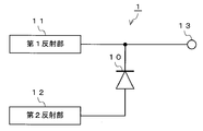
- FIG. 1 is a schematic explanatory diagram of the configuration and operation of a high-frequency oscillator according to the present embodiment.
- the schematic diagram which shows the state of the signal of the high frequency oscillator in operation
- FIG. 3 is an exemplary diagram of a line pattern formed on a substrate of an oscillator according to the present embodiment.
- the actual measurement figure of the temperature change of the oscillator of a present Example. 6 is an equivalent circuit showing a modification of the configuration of the high-frequency oscillator according to the present embodiment.
- FIG. 1 is a schematic explanatory diagram of the configuration and operation of the high-frequency oscillator according to the present embodiment.
- the high-frequency oscillator 1 is a self-excited two-terminal oscillator that excites oscillation by a seed signal. Thermal noise is used for the seed signal. Thermal noise is white noise and has a spectrum of all frequencies up to the submillimeter wave band, so it is suitable for a seed signal.
- the high frequency oscillator 1 includes a negative resistance element 10 that guides an input signal in a forward direction.
- the negative resistance element 10 is an active element having a reflection coefficient (reflection gain) exceeding 1.0, as described in the prior art, and has a cathode terminal (first terminal) and an anode terminal (second terminal). Have.
- a first reflecting portion 11 is provided at the cathode terminal.
- a second reflecting portion 12 is provided at the anode terminal.
- Each of the first reflecting portion 11 and the second reflecting portion 12 is composed of a distributed constant line having an end portion (hereinafter referred to as “high frequency open end”) that totally reflects a signal without using a ground conductor or a via hole.
- the distributed constant line is formed by, for example, printed wiring on a dielectric substrate.
- the negative resistance element 10 is flip-chip connected to a distributed constant line that is printed. The installation position of the negative resistance element 10 is determined in consideration of the impedance of the oscillation signal.
- the high-frequency open end can be easily realized by setting the electrical length of the distributed constant line to a predetermined length determined according to the oscillation frequency. The electrical length of the distributed constant line will be described in detail later.
- the outline of the oscillation operation in the high-frequency oscillator 1 is as follows. First, the seed signal is input to the cathode terminal of the negative resistance element 10. Then, a part of the light is reflected with a reflection coefficient exceeding 1.0 and goes to the first reflecting part 11, and the other part passes through the negative resistance element 10, and further passes through the anode terminal to the second reflecting part. Head to 12 (reverse direction). The 1st reflection part 11 and the 2nd reflection part 12 each totally reflect a propagation signal by a high frequency open end. The signal totally reflected by the second reflecting portion 12 propagates in the direction of the cathode terminal (forward direction) through the anode terminal of the negative resistance element 10, part of which passes through the negative resistance element 10 and the rest is the first. 2 Returning to the reflection unit 12, total reflection is performed at the high-frequency open end. The signal that has passed through the negative resistance element 10 from the second reflecting portion 12 is directed to the first reflecting portion 11 and totally reflected at the high-frequency open end thereof.
- the cathode terminal of the negative resistance element 10 eventually passes through the negative reflection element 10 from the second reflection section 12 to the first reflection section 11 and the signal totally reflected by the first reflection section 11.
- a signal obtained by adding the signal totally reflected at the high-frequency open end is input.
- the operation input to the cathode terminal is repeated.
- the magnitude (amplitude) of the signal increases until the negative resistance element 10 is limited within the range of current and voltage at which it operates.
- standing waves are generated in the first reflecting portion 11 and the second reflecting portion 12.
- the high frequency oscillator 1 generates an oscillation signal corresponding to a standing wave and outputs it from an output unit described later.
- FIG. 2 is a diagram schematically showing a signal flow when the high-frequency oscillator 1 is operating.
- the oscillation signal is output from the output unit 13 to the outside.
- the output unit 13 may be basically provided in any part, but FIG. 2 shows an example in which the output unit 13 is provided between the cathode terminal of the negative resistance element 10 and the first reflecting unit 11.
- the reflection coefficient viewed from the output unit 13 of the first reflection unit 11 is “ ⁇ 1”
- the reflection coefficient viewed from the negative resistance element 10 of the second reflection unit 12 is “ ⁇ 2”
- the negative resistance element. 10 and the reflection coefficient viewed from the output unit 13 of the second reflecting unit 12 are represented by “ ⁇ D”.
- the negative resistance element 10 is represented by a 2-port S parameter.
- the S parameter is expressed by elements S11, S21, S12, and S22.
- S ⁇ b> 11 represents the magnitude (amplitude) of the signal that the signal from the first reflection unit 11 is reflected by the negative resistance element 10.
- S ⁇ b> 21 represents the magnitude of the signal through which the signal from the first reflection unit 11 passes through the negative resistance element 10.
- S ⁇ b> 12 represents the magnitude of the signal that the signal from the second reflection unit 12 passes through the negative resistance element 10.
- S ⁇ b> 22 represents the magnitude of the signal that the signal from the second reflection unit 12 is reflected by the negative resistance element 10.
- the reflection coefficient ⁇ D can be expressed by Equation 1 using this S parameter.
- the second term of Equation 1 is hereinafter referred to as “resonance term”.
- ⁇ D S11 + (S21 ⁇ S12 ⁇ ⁇ 2 / (1-S22 ⁇ ⁇ 2)) (Formula 1)
- the oscillation condition of the high-frequency oscillator 1 is that the negative resistance element 10 has a reflection gain exceeding 1.0, and the signal reflected by the first reflection unit 11 is positively fed back to the negative resistance element 10. is there. That the negative resistance element 10 has a reflection gain of 1.0 or more is expressed by Expression 2, and that the signal reflected by the first reflection unit 11 is positively fed back is expressed by Expression 3.
- Im (*) 0 indicates that the imaginary part is 0, that is, there is no phase difference between the output signal and the input signal (in-phase, that is, the phase difference is an integral multiple of 360 °, or an integral multiple of 2 ⁇ radians).
- Im ( ⁇ D * ⁇ 1) 0 (Formula 3)
- the high-frequency oscillator 1 includes the negative resistance element 10, the first reflection unit 11, and the second reflection unit 12 in addition to the oscillation conditions of Equation 2, Equation 3 to Equation 4, and Equation 5, The conditions of Formula 6 and Formula 7 were also satisfied. More specifically, the electrical length of the distributed constant line is designed to satisfy the conditions of Equations 3 and 7 (positive feedback). Further, the distributed constant lines of the first reflecting portion 11 and the second reflecting portion 12 are configured to have a high-frequency open end so as to satisfy the conditions of Expressions 2 and 6. As a result, the denominator of the resonance term is reduced, and most of the signal totally reflected by the second reflecting portion 12 returns to the first reflecting portion 11 and efficient oscillation is possible. The actual measurement result of this point will be described later based on an example.
- the distributed constant line has a high-frequency open end, so that the Q value can be prevented from decreasing.
- the Q value is a dimensionless number representing the state of vibration, and the larger the value, the more stable the vibration.
- this Q value may decrease, but in the present embodiment, the first reflection unit 11 and the second reflection unit 12 totally reflect the propagated signal at the high-frequency open end. A decrease in the Q value can be prevented.
- phase noise can be reduced. That is, in the process of multiple reflection in which total reflection by the first reflection unit 11 and the second reflection unit 12 is repeated, the phase of the signal is quickly adjusted as if it were an oscillator using a waveguide, and the phase noise is reduced. Also, spurious oscillation and harmonic oscillation are suppressed. The actual measurement result of this point will be described later based on an example. As a result, excellent oscillation performance can be realized.
- the utility of the present embodiment is that not only the excellent oscillation performance can be realized, but also the manufacturing problems left by the conventional high-frequency oscillator in which the grounded end is formed on the distributed constant line can be solved.
- the formation of the high-frequency open end on the distributed constant line can be easily realized only by printed wiring to a substrate such as a dielectric, which is advantageous in terms of cost in that at least a ground conductor or similar parts are unnecessary. It becomes. Further, since the ground end is not formed, it is not necessary to use via holes or similar parts, and the problem of fluctuations in the electrical length (phase) of the distributed constant line during the formation of these materials and their processing can be solved.
- FIG. 3 is an equivalent circuit of the high-frequency oscillator 1.
- the negative resistance element 10 is expressed as a diode.
- the second reflecting unit 12 is connected to the anode terminal of the negative resistance element 10.
- the high-frequency oscillator 1 is very simple not only in terms of structure but also in terms of an equivalent circuit.
- the oscillator 2 outputs an oscillation signal having an oscillation frequency of 79 [GHz], which is used in, for example, a high resolution radar.
- a substrate an aluminum nitride substrate having a relative dielectric constant of 9 was used.
- a microstrip line was formed on the substrate by printed wiring. In consideration of the skin effect, the microstrip line is formed of a multi-layer metal film. Specifically, a titanium film was formed to ensure adhesion strength with the substrate, and the metal film exposed at the uppermost layer was a metal layer (gold plating) having the highest corrosion resistance and high conductivity.
- FIG. 4 shows the line pattern of distributed constant lines formed on the substrate.
- FIG. 5 shows an equivalent circuit when a negative resistance element is mounted on the line pattern. Parts corresponding to the parts shown in FIGS. 1 to 3 are denoted by the same reference numerals as those parts.
- two negative resistance elements 101 and 102 having the same characteristics are flip-chip connected to predetermined positions of the line pattern.
- these negative resistance elements 101 and 102 are indicated by diode symbols, and bonding pads are formed. It is shown by a circular broken line. Gunn diodes were used for the negative resistance elements 101 and 102, respectively.
- the accuracy of the line pattern and the mounting accuracy are ⁇ 5 ⁇ m or less. This is an electrical length (phase) of 79 [GHz] and 1.5 degrees or less, and can be easily adjusted by phase control.
- the first reflecting portion 11 described above is shared, and the cathode terminals of the negative resistance elements 101 and 102 are commonly connected to the first reflecting portion 11. Further, the two second reflection parts 12 described above are formed, one anode terminal of one negative resistance element 101 is formed in one second reflection part 121, and the other negative resistance element 102 is formed in the other second reflection part 122. The anode terminals were connected independently.
- the 1st reflection part 11 and the 2nd reflection parts 121 and 122 have a high frequency open end, respectively.
- the electrical length (L1) of the first reflector 11 is the length of the wide distributed constant line in the longitudinal direction, and satisfies the condition of Equation 3 at an oscillation frequency of 79 [GHz].
- the electric length (L2) of each of the second reflecting portions 121 and 122 is the length to the outer end closest to the anode terminal of each of the negative resistance elements 101 and 102 in the example of FIG. 5, and is 79 [GHz].
- the conditions of Equations 6 and 7 are satisfied at the oscillation frequency of
- the bias portion 14 is formed integrally with the first reflecting portion 11.
- the bias portion 151 is integrally formed with one second reflecting portion 121
- the bias portion 152 is integrally formed with the other second reflecting portion 122.
- Each of the bias portions 14, 151, 152 is formed by forming a ⁇ / 4 radial stub at the central portion of the ⁇ / 4 microstrip line.
- Each bias part 14, 151, 152 is formed to operate the negative resistance elements 101, 102 in the negative resistance region.
- the first reflection unit 11 and the output unit 13 are inductively connected via a band pass filter 16.
- the band pass filter 16 passes only a desired oscillation frequency.
- the negative resistance element 101, the second reflection part 121, and the bias part 151, and the negative resistance element 102, the second reflection part 122, and the bias part 152 are symmetrical with respect to the first reflection part 11. Arranged. As a result, the two negative resistance elements 101 and 102 oscillate in phase. Therefore, even when the two high-frequency oscillators 1 are mounted and the oscillator 2 is configured, a stable oscillation operation can be maintained. In addition, all components except the negative resistance elements 101 and 102 are formed by one layer of printed wiring. Therefore, processing / manufacturing is extremely easy, and the manufacturing cost can be significantly reduced.
- the output power was measured while intentionally changing the line length (L2).
- the output power was measured when only the portion corresponding to the second reflectors 121 and 122 was grounded as in the conventional high-frequency oscillator (referred to as “conventional product” for convenience).
- the output power of the conventional product was 12.5 [dBm].
- the output power in this embodiment is 12.6 [dBm] when the line length (L2) is 360 [ ⁇ m]
- the line length (L2) was 13.5 [dBm] at 400 [ ⁇ m].
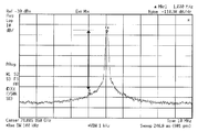
- phase noise is a characteristic that characterizes oscillation performance.
- phase noise it is possible to easily determine how steep the bottom of the spectrum of the oscillation signal is with a spectrum analyzer.
- the actual measurement result of the spectrum of the oscillation signal from the oscillator 2 is shown in FIG.
- the difference between the power at the oscillation peak and the power at 1 [MHz] detuning is approximately 60 [dB].
- phase noise of ⁇ 110 [dBc / Hz] is a low value comparable to the phase noise of an oscillator having a waveguide resonator, and has been confirmed as an oscillator having a planar structure using a distributed constant line. Currently, the best value.
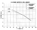
- the temperature change of the oscillator 2 was also measured.
- the actual measurement result is shown in FIG.
- the conventional product was 0.047 [dB / ° C.], whereas the oscillator 2 was 0.040 [dB / ° C.]. This value is slightly better than the conventional product. No spurious oscillation or harmonic oscillation was observed in the measurable range (direct current component (DC) to 110 [GHz]).
- DC direct current component
- the oscillator 2 of the present example can realize excellent oscillation performance while having a simple planar structure including only the substrate having the line pattern on the front side and the negative resistance elements 101 and 102.
- FIG. 8 is an equivalent circuit showing a modification of the high-frequency oscillator 1.
- the same parts as those shown in FIG. 3 are denoted by the same reference numerals.
- the high-frequency oscillator 3 shown in FIG. 8 is an anti-parallel connection of two negative resistance elements having the same characteristics, and this is formed as one negative resistance element (chip) 30.
- Anti-parallel connection means that negative resistance elements are connected in parallel with the polarity reversed. In such a configuration, one negative resistance element is transmitted in the forward direction from the first reflecting portion 11 to the second reflecting portion 12, and the other negative resistance is transmitted from the second reflecting portion 12 to the first reflecting portion 11. It is transmitted in the forward direction by the element. Therefore, insertion loss of the negative resistance element can be suppressed, and the oscillation efficiency is further increased.
- the ground end portion may act as a high-frequency open end.
- the manufacturing cost cannot be reduced as long as the ground conductor and the via hole are required.
- a function equivalent to that of the grounding end is realized without forming a ground conductor in the second reflecting portion 12 (that is, at a low cost). can do.
Landscapes
- Inductance-Capacitance Distribution Constants And Capacitance-Resistance Oscillators (AREA)
Abstract
【課題】ビアホールなどを用いて接地端を形成しなくとも良好な共振特性を得ることができる簡易な構造の高周波発振器を提供する。 【解決手段】高周波発振器1は、2端子の負性抵抗素子10を備える。負性抵抗素子10のカソード端子には、高周波開放端を有する第1反射部11が接続される。負性抵抗素子10のアノード端子には、同じく高周波開放端を有する第2反射部12が接続される。高周波発振器1は、負性抵抗素子10で反射された信号と第1反射部11及び第2反射部12の各々で全反射された信号とを同相で足し合わせることにより、信号を発振する。
Description
本発明は、マイクロ波帯以上、特にミリ波帯(30[GHz]~300[GHz])の発振信号を出力する自励型の高周波発振器に関する。
自励型の高周波発振器として、2端子発振器が知られている。2端子発振器は、発振条件を満たす能動素子と共振部とを組み合わせて構成される。発振条件を満たす能動素子は、インピーダンスの実部(抵抗成分)が負となり、反射係数が1.0を超える素子であり、例えばGunnダイオードやトンネルダイオードなどがそれに該当する。このような能動素子に信号を入力すると、入力した信号よりも大きな振幅の信号が反射される。つまり、反射利得(増幅作用)を有するものとなる。そのため、このような能動素子は「負性抵抗素子」と呼ばれる。2端子発振器では、共振部が負性抵抗素子により反射される信号を正帰還してその負性抵抗素子に再入力することで発振が起きる。
2端子発振器では、発振された信号(以下、「発振信号」という)の周波数(以下、「発振周波数」という)がマイクロ波帯以上の高周波帯になると、LC共振回路のように受動素子を用いた回路で共振部の機能を実現することが困難になる。そのため、マイクロ波帯以上の帯域で使用される2端子発振器では、共振部を分布定数線路で実現するのが一般的である。
共振部を分布定数線路で実現した発振器として、例えば特許文献1に開示された高周波発振器が知られている。この高周波発振器は2端子発振器ではないが、反射利得によって高周波の発振信号を発振させる点では、上述した2端子発振器と同じになる。この高周波発振器では、発振用トランジスタのエミッタ側に接地電位となる一対のビアホールが設けられている。ビアホールは、基板の表面に形成されたマイクロストリップ線路の形成面と基板の裏面に形成された接地導体とを導通するために用いられる。そのため、ビアホールが接地電位となる。ビアホールには、金属導体あるいは金属メッキが施された硬質材が用いられる。また、これらのビアホール間に、同一線路長のマイクロストリップ線路で構成された2つのショートスタブが設けられている。ショートスタブは、マイクロストリップ線路に接地(ショート)端を形成するためのスタブであり、当該形成部分のインピーダンスを固定にして発振動作を安定にするために用いられる。2つのショートスタブの間には、発振用トランジスタのエミッタが接続される。
また、特許文献2には、FET(Field effect transistor)のソース端子に負性抵抗発生用の容量性のショートスタブを設ける発振器が開示されている。このショートスタブもまた、ビアホールを通じて分布定数線路に接地端を形成するためのスタブである。特許文献2に開示された高周波発振器では、ショートスタブによる接地位置がワイヤボンディングにより変更可能であり、ショートスタブの接地位置を調整することにより、一定の周波数範囲で安定した発振動作を行うことができる。
特許文献1,2に開示された高周波発振器は、安定した発振動作が可能になる利点はあるが、その製造面で課題を残すものである。
まず、分布定数線路の端部を接地端とする際に接地導体が必要となる。そのため、製造コストを低減させることができないという問題がある。また、接地導体と導通するビアホールの存在によって分布定数線路の電気長が変動するという問題もある。分布定数線路の電気長は、伝搬する信号の位相を決めるものなので、電気長が変動すると複数の信号の位相を同期させることが困難となる。ビアホールは、その材質にもよるが、一般にミリ波帯になると、寄生インダクタンスや抵抗成分の損失の影響が大きくなり、分布定数線路の電気長を変動させてしまう。
まず、分布定数線路の端部を接地端とする際に接地導体が必要となる。そのため、製造コストを低減させることができないという問題がある。また、接地導体と導通するビアホールの存在によって分布定数線路の電気長が変動するという問題もある。分布定数線路の電気長は、伝搬する信号の位相を決めるものなので、電気長が変動すると複数の信号の位相を同期させることが困難となる。ビアホールは、その材質にもよるが、一般にミリ波帯になると、寄生インダクタンスや抵抗成分の損失の影響が大きくなり、分布定数線路の電気長を変動させてしまう。
例えば比誘電率3、厚み0.25[mm]の基板上に、接地端を有する分布定数線路を形成し、80[GHz]の信号を伝搬させる場合を例に挙げて説明する。分布定数線路にはλ/4線路(90度の電気長)を用いるものとする。信号の波長は2.2[mm]なので、λ/4線路の電気長は0.55[mm]となり、基板の表面の線路パターンと裏面の接地導体とを導通させるために基板を貫通するビアホールの電気長は、41度(=(0.25/0.55)×90度)となる。この電気長が信号の位相に与える影響は大きい。負性抵抗素子を用いた高周波発振器では、上述したように反射利得が1.0を超えるため、信号の位相がずれた場合の修正が困難となる。そのため、緻密な位相制御が不可欠となる。このように、ビアホールを用いて接地端を形成する場合は、電磁界解析などの高度の設計手法が必要となるため、コスト増を招く。
分布定数線路に接地端を形成する際の加工上の問題もある。80[GHz]の信号を伝搬させる分布定数線路の場合、基板上の線路パターンの一般的な加工精度(特性変動の許容範囲)は、金属厚みが3[μm]の場合で±3[μm]、金属厚みが18[μm]の場合で±20[μm]である。また、ビアホールの位置精度は±50[μm]、ビアホールを埋め込むホールの最少直径は100[μm]、ホールの直径の精度は±30[μm]である。そのため、ビアホールを形成するには、高度の加工技術が必要となり、コスト増を招く。
分布定数線路としてコプレーナ導波路が用いられる場合がある。コプレーナ導波路は、誘電体基板の表面に伝送路と接地パターンとが形成された導波路であり、線路パターンの加工精度はさほど厳しくない。しかし、コプレーナ導波路であっても、伝送路に対する接地パターンの同相性を保つ必要があるため、ビアホールを周密に設けるのが一般的である。そのため、上述したビアホールの加工上の問題が生じる。
ビアホールが必要となるのは接地導体を使用するためであり、接地導体を使用するのは、分布定数線路に接地端を形成するためである。そして、接地端を形成するのは、高周波発振器における電気的特性を良好にして発振動作を安定にするためである。分布定数線路に接地端を形成しなくとも、接地端を形成した場合と同等以上の電気的特性を可能にする簡易な構造であれば、上記の問題は解決する。
本発明は、分布定数線路を用いた場合において、接地端を形成した場合と同等以上の電気的特性を得ることができる簡易な構造の高周波発振器を提供することを課題とするものである。
本発明は、分布定数線路を用いた場合において、接地端を形成した場合と同等以上の電気的特性を得ることができる簡易な構造の高周波発振器を提供することを課題とするものである。
上記課題を解決する本発明の高周波発振器は、反射利得を有する2端子の負性抵抗素子と、それぞれ伝搬信号を接地導体を要することなく反射させるために分布定数線路で形成された第1反射部および第2反射部とを備えており、前記第1反射部が前記負性抵抗素子の第1端子、前記第2反射部が前記負性抵抗素子の第2端子にそれぞれ接続されており、これにより前記第2反射部で反射された信号が前記負性抵抗素子を通じて前記第1反射部へ正帰還して発振信号を生成する高周波発振器である。
本発明によれば、第1の反射部及び第2の反射部が接地導体を要することなく、その高周波開放端で信号を反射させる。また、負性抵抗素子により反射された信号と第1の反射部及び第2の反射部の各々の高周波開放端で反射された信号との足し合わせにより発生する発振信号を出力する。そのため、製作が容易で廉価な構成でありながら、効率よく発振動作を行うことができる。
以下、本発明の実施の形態例を説明する。図1は、本実施形態に係る高周波発振器の構成および動作の概略説明図である。この高周波発振器1は、種信号により発振を励起する自励型の2端子発振器である。種信号には熱雑音を用いる。熱雑音はホワイトノイズであり、サブミリ波帯までのすべての周波数のスペクトルを持つので、種信号に適している。
高周波発振器1は、入力された信号を順方向に導く負性抵抗素子10を備える。負性抵抗素子10は、従来技術で説明したものと同様、反射係数(反射利得)が1.0を超える能動素子であり、カソード端子(第1端子)とアノード端子(第2端子)とを有する。カソード端子には、第1反射部11が設けられる。アノード端子には第2反射部12が設けられる。
第1反射部11及び第2反射部12は、いずれも接地導体やビアホールを用いることなく、信号を全反射させる端部(以下、「高周波開放端」という)を有する分布定数線路で構成される。分布定数線路は、例えば誘電体の基板上にプリント配線することで形成する。負性抵抗素子10は、プリント配線された分布定数線路にフリップチップ接続される。負性抵抗素子10の設置位置は、発振信号のインピーダンスを考慮して決められる。高周波開放端は、分布定数線路の電気長を発振周波数に応じて決まる所定長にすることで容易に実現することができる。分布定数線路の電気長については、後で詳しく説明する。
高周波発振器1における発振動作の概要は以下のとおりである。まず、上記の種信号が、負性抵抗素子10のカソード端子に入力される。そして、その一部は1.0を超える反射係数で反射されて第1反射部11に向かい、他の一部は負性抵抗素子10を通過し、さらに、そのアノード端子を経て第2反射部12に向かう(逆方向)。第1反射部11および第2反射部12は、それぞれ伝搬信号を高周波開放端で全反射させる。第2反射部12で全反射された信号は、負性抵抗素子10のアノード端子を通じてカソード端子の方向(順方向)に伝搬し、その一部が負性抵抗素子10を通過し、残りは第2反射部12に戻り、高周波開放端で全反射される。第2反射部12から負性抵抗素子10を通過した信号は、第1反射部11に向かい、その高周波開放端で全反射される。
負性抵抗素子10のカソード端子には、結局、第1反射部11で全反射された信号と、第2反射部12から負性抵抗素子10を通過して第1反射部11に向かい、その高周波開放端で全反射された信号とが足し合わされた信号が入力される。第1反射部11及び第2反射部12の各々の分布定数線路の電気長を、カソード端子に入力される各信号の位相が合う長さに設計することで、足し合わされた信号は、すべて同相となる。つまり、正帰還となる。以後、負性抵抗素子10、第1反射部11および第2反射部12の高周波開放端による信号の全反射が繰り返されることで信号が同相で足し合わされ、足し合わされた信号が負性抵抗素子10のカソード端子に入力される動作が繰り返される。その結果、負性抵抗素子10が動作する電流および電圧の範囲でリミットされるまで信号の大きさ(振幅)が増大する。このような状態では、第1反射部11および第2反射部12に定在波が生じる。高周波発振器1は、定在波に応じた発振信号を生成し、これを後述する出力部から出力する。
次に、高周波発振器1における発振条件およびそれを満たすための第1反射部11及び第2反射部12の各々の分布定数線路の電気長について説明する。図2は、高周波発振器1が動作しているときの信号の流れを模式的に示した図である。発振信号は、出力部13から外部へ出力される。出力部13は、基本的にはどの部位に設けても良いが、図2では、負性抵抗素子10のカソード端子と第1反射部11との間に設ける例が示されている。
図2では、また、第1反射部11の出力部13から見た反射係数を「Γ1」、第2反射部12の負性抵抗素子10から見た反射係数を「Γ2」、負性抵抗素子10及び第2反射部12の出力部13から見た反射係数を「ΓD」で表している。また、負性抵抗素子10を2ポートのSパラメータで表している。
Sパラメータは、S11,S21,S12,S22の要素で表現される。S11は、第1反射部11からの信号が負性抵抗素子10で反射される信号の大きさ(振幅)を表す。S21は、第1反射部11からの信号が負性抵抗素子10を通過する信号の大きさを表す。S12は、第2反射部12からの信号が負性抵抗素子10を通過する信号の大きさを表す。S22は、第2反射部12からの信号が負性抵抗素子10で反射される信号の大きさを表す。反射係数ΓDは、このSパラメータを用いて式1で表すことができる。式1の第二項を、以後「共振項」と呼ぶ。
ΓD=S11+(S21・S12・Γ2/(1-S22・Γ2)) (式1)
ΓD=S11+(S21・S12・Γ2/(1-S22・Γ2)) (式1)
高周波発振器1の発振条件は、負性抵抗素子10が1.0を超える反射利得を有し、かつ、第1反射部11で反射された信号が負性抵抗素子10に正帰還されることである。負性抵抗素子10が1.0以上の反射利得を有することは式2で表され、第1反射部11により反射された信号が正帰還されることは式3で表される。Im(*)=0は虚部が0、すなわち出力信号と入力信号の位相差が無い(同相すなわち位相差が360°の整数倍、ないし2πラジアンの整数倍となる)ことを表す。
|ΓD|・|Γ1|>1 (式2)
Im(ΓD*Γ1)=0 (式3)
|ΓD|・|Γ1|>1 (式2)
Im(ΓD*Γ1)=0 (式3)
第2反射部12に相当する部分が接地端となる従来の高周波発振器の場合、反射係数Γ2は、略「-1」となる。そのため、カソード端子から負性抵抗素子10を通過した信号が発振動作に活用されていない。つまり、従来の高周波発振器では、以下の式4、式5の発振条件のもとで設計されていたといえる。式4,式5の意味合いは、式2,式3と同じである。
|S11|・|Γ1|>1 (式4)
Im(S11*Γ1)=0 (式5)
|S11|・|Γ1|>1 (式4)
Im(S11*Γ1)=0 (式5)
これに対して、本実施形態の高周波発振器1では、式1の共振項に着目し、負性抵抗素子10を通過して第2反射部12に到達した信号を発振動作に積極的に活用する仕組を創案した。すなわち、式1の共振項の分母が小さくなるようにし、第1反射部11から負性抵抗素子10を経て第2反射部12に向かう信号の多くを第1反射部11へ戻すようにした。このときの条件を式6、式7に示す。
|S22|・|Γ2|を極力大きく(式6)
Im(S22*Γ2)=0 (式7)
式6は、|Γ2|を極力大きくすることを表す。
|S22|・|Γ2|を極力大きく(式6)
Im(S22*Γ2)=0 (式7)
式6は、|Γ2|を極力大きくすることを表す。
すなわち、本実施形態では、高周波発振器1を、負性抵抗素子10と第1反射部11及び第2反射部12とが、式2,式3ないし式4,式5の発振条件のほかに、式6,式7の条件をも満たすようにした。より詳しくは、分布定数線路の電気長を式3,式7の条件(正帰還)を満たす長さに設計した。また、式2,式6の条件を満たすように、第1反射部11及び第2反射部12の分布定数線路が高周波開放端を有するように構成した。これにより、共振項の分母が小さくなり、第2反射部12で全反射された信号の多くが第1反射部11に戻り、効率の良い発振が可能となった。この点の実測結果については、後で実施例を基に説明する。
分布定数線路が高周波開放端を有することで、Q値の低下を防止することもできる。Q値は振動の状態を現す無次元数であり、この値が大きいほど振動が安定であることを意味する。分布定数線路を用いる場合、このQ値が低下するおそれがあるが、本実施形態では、第1反射部11及び第2反射部12が、伝搬してきた信号を高周波開放端で全反射させるので、Q値の低下を防止することができる。
上記のように効率の良い発振が可能になることにより、位相雑音の低下が可能になる。すなわち、第1反射部11及び第2反射部12による全反射を繰り返す多重反射の過程で、あたかも導波管による発振器のように信号の位相が迅速に揃えられ、位相雑音が低くなる。また、発振のスプリアスや高調波発振も抑制される。この点の実測結果については、後で実施例を基に説明する。これによって優れた発振性能を実現することができる。
本実施形態の効用は、優れた発振性能を実現できるだけでなく、分布定数線路に接地端を形成している従来の高周波発振器が残す製造面の課題も解決できる点にある。第1に、分布定数線路への高周波開放端の形成は、誘電体などの基板へのプリント配線だけで簡易に実現できることであり、少なくとも接地導体ないし同種部品が不要となる点でコスト面で有利となる。また、接地端を形成しないからビアホールや同種部品を使用する必要がなくなり、これらの材質およびその形成、加工の際の分布定数線路の電気長(位相)変動の問題を解決できる。
図3は、高周波発振器1の等価回路である。負性抵抗素子10はダイオードとして表現される。第2反射部12は、負性抵抗素子10のアノード端子に接続される。このように、高周波発振器1は、構造面のみならず、等価回路的にもきわめて簡易なものとなる。
<実施例>
次に、高周波発振器1の実施例について説明する。ここでは、1つの基板上に上述した二つの高周波発振器1を実装した発振器2の例を説明する。この発振器2は、例えば高分解レーダに用いられる、発振周波数が79[GHz]の発振信号を出力する。基板には、比誘電率9の窒化アルミニウム基板を用いた。基板上には、プリント配線でマイクロストリップ線路を形成した。マイクロストリップ線路は、表皮効果を考慮して、複数階層の金属膜で形成した。具体的には、基板との接着強度を確保するためにチタン膜を形成し、最上層で露出する金属膜を、耐蝕性が最も高くかつ伝導度の高い金属層(金メッキ)とした。
次に、高周波発振器1の実施例について説明する。ここでは、1つの基板上に上述した二つの高周波発振器1を実装した発振器2の例を説明する。この発振器2は、例えば高分解レーダに用いられる、発振周波数が79[GHz]の発振信号を出力する。基板には、比誘電率9の窒化アルミニウム基板を用いた。基板上には、プリント配線でマイクロストリップ線路を形成した。マイクロストリップ線路は、表皮効果を考慮して、複数階層の金属膜で形成した。具体的には、基板との接着強度を確保するためにチタン膜を形成し、最上層で露出する金属膜を、耐蝕性が最も高くかつ伝導度の高い金属層(金メッキ)とした。
基板に形成した分布定数線路の線路パターンを図4に示す。また、線路パターンに負性抵抗素子を実装したときの等価回路を図5に示す。図1ないし図3に示した部品に対応する部分には当該部品と同じ符号を付してある。本例では同一特性の二つの負性抵抗素子101,102を線路パターンの所定位置にフリップチップ接続するが、図4では、これらの負性抵抗素子101,102をダイオード記号で示し、ボンディングパッドを円破線で示してある。各負性抵抗素子101,102にはGunnダイオードを用いた。線路パターンの精度、実装精度は±5μm以下である。これは電気長(位相)にして79[GHz]で1.5度以下であり、位相制御で容易に調整が可能な範囲である。
この発振器2では、上述した第1反射部11を共用し、この第1反射部11に負性抵抗素子101、102の各々のカソード端子を共通接続した。また、上述した第2反射部12を2つ形成し、一方の第2反射部121に一方の負性抵抗素子101のアノード端子、他方の第2反射部122に他方の負性抵抗素子102のアノード端子をそれぞれ独立に接続した。第1反射部11、第2反射部121,122は、それぞれ高周波開放端を有するものとなっている。第1反射部11の電気長(L1)は、図5の例では幅の広い分布定数線路の長尺方向の長さであり、79[GHz]の発振周波数で式3の条件を満たす。第2反射部121,122のそれぞれの電気長(L2)は、図5の例では各負性抵抗素子101,102のアノード端子と最も近い外端部までの長さであり、79[GHz]の発振周波数で式6、式7の条件を満たす。
本実施例では、第1反射部11にバイアス部14を一体形成した。また、一方の第2反射部121にバイアス部151を一体形成し、他方の第2反射部122にもバイアス部152を一体形成した。各バイアス部14,151,152は、各々、λ/4-マイクロストリップ線路の中央部にλ/4-ラディアル・スタブを形成したものである。各バイアス部14,151,152は、負性抵抗素子101,102を、負性抵抗領域で動作させるために形成したものである。
第1反射部11と出力部13とは、バンド・パス・フィルタ16を介して誘導接続されるようにした。バンド・パス・フィルタ16は、所望の発振周波数だけを通過させる。
第1反射部11と出力部13とは、バンド・パス・フィルタ16を介して誘導接続されるようにした。バンド・パス・フィルタ16は、所望の発振周波数だけを通過させる。
この発振器2では、第1反射部11を挟んで、負性抵抗素子101、第2反射部121およびバイアス部151と、負性抵抗素子102、第2反射部122およびバイアス部152とをそれぞれ対称に配置した。これにより2つの負性抵抗素子101,102が同相で発振動作する。そのため、2つの高周波発振器1を実装して発振器2を構成しても、安定した発振動作を維持することができる。また、負性抵抗素子101,102を除くいずれの部品も1層のプリント配線で形成される。したがって、加工・製造がきわめて容易であり、製造コストを格段に低減させることができる。
この発振器2において、第2反射部121,122の効果を確認するために、線路長(L2)を意図的に変えて出力電力を測定してみた。また、第2反射部121,122に相当する部分だけを従来の高周波発振器のように接地端にした場合(便宜上、「従来品」という)の出力電力を測定してみた。従来品の出力電力は12.5[dBm]であった。これに対し、本実施例の場合の出力電力は、線路長(L2)が360[μm]で12.6[dBm]、線路長(L2)が380[μm]で12.5[dBm]、線路長(L2)が400[μm]で13.5[dBm]であった。つまり、第2反射部121,122の電気長(L2)を適切に設計することで、多大な製造コストをかけて接地端を形成した従来品と同じか、それ以上の出力電力が得られることが確認された。なお、上記の比較は従来品と本発明を同一条件で比較した一例であり、発明の効果を限定するものではない。
また、発振性能を特徴づける特性として位相雑音がある。位相雑音は、簡易には、発振信号のスペクトラムの裾がどれだけ急峻かをスペクトラム・アナライザーにより求めることができる。発振器2からの発振信号のスペクトラムの実測結果を図6に示す。図6では、100kHz周波数帯域ごとの電力を測定し表示している(Resolution Band Width=100kHzが図6左下に表示されている。)。図6中の矢印で示したように、発振ピークの電力と1[MHz]離調での電力差が概ね60[dB]である。これを1[Hz]あたりの電力で表すと、100[kHz]と1[Hz]の帯域比の100,000=50[dB]を加え、110dBとなる。正確な測定値は右上に表示されている。キャリア信号に対する電力比では、単位は[dBc/Hz]となる。測定の結果では、出力電力を3dBほど減少させたところで最も低い位相雑音となり、-110[dBc/Hz]が得られている。この位相雑音は、従来品の位相雑音が-105~-100[dBc/Hz]であるのに対して、5[dBc/Hz]以上良い結果である。これは、上述したように、第2反射部121,122の高周波開放端による全反射を繰り返す多重反射の過程で信号の位相が迅速に揃えられ、雑音が低くなったためである。これによっても、この実施例による発振器2の有効性が確認された。-110[dBc/Hz]の位相雑音は、導波管型の共振器を持つ発振器の位相雑音に匹敵する低い値であり、分布定数線路を用いた平面構造の発振器として確認されている中では、現在のところ最も良い値である。
発振器2の温度変化についても測定してみた。その実測結果を図7に示す。摂氏25度~85度において、発振器2は、従来回路よりも温度変動が少なかった。従来品が0.047[dB/℃]に対し、発振器2は0.040[dB/℃]であった。この数値は、従来品よりも若干良い性能である。なお、発振のスプリアス、高調波発振は、測定可能な範囲(直流成分(DC)~110[GHz])では、観測されなかった。
このように、本実施例の発振器2では、表側に線路パターンのみを有する基板と負性抵抗素子101,102だけという簡易な平面構造でありながら、優れた発振性能を実現できることが確認された。
このように、本実施例の発振器2では、表側に線路パターンのみを有する基板と負性抵抗素子101,102だけという簡易な平面構造でありながら、優れた発振性能を実現できることが確認された。
<変形例>
本実施形態および本実施例では、負性抵抗素子10,101,102として、Gunnダイオードを用いた場合の例を説明したが、負性抵抗素子10,101,102として、トンネルダイオードを用いることもできる。また、本実施形態では、高周波発振器1に1つの負性抵抗素子を用いた場合の例を説明したが、本発明は、この例に限定されない。
本実施形態および本実施例では、負性抵抗素子10,101,102として、Gunnダイオードを用いた場合の例を説明したが、負性抵抗素子10,101,102として、トンネルダイオードを用いることもできる。また、本実施形態では、高周波発振器1に1つの負性抵抗素子を用いた場合の例を説明したが、本発明は、この例に限定されない。
図8は、高周波発振器1の変形例を示した等価回路である。図3に示したものと同じ部品については、同じ符号を付してある。図8に示す高周波発振器3は、同一特性の2つの負性抵抗素子をアンチパラレル接続し、これを一つの負性抵抗素子(チップ)30としたものである。アンチパラレル接続とは、負性抵抗素子が極性を逆にして並列接続することをいう。このような構成では、第1反射部11から第2反射部12へは一方の負性抵抗素子で順方向で伝達され、第2反射部12から第1反射部11へは他方の負性抵抗素子で順方向で伝達される。そのために、負性抵抗素子の挿入損失を抑制することができ、発振効率が更に高くなる。
なお、従来品において、分布定数線路の長さを調整することにより、接地端の部分が高周波開放端として作用する場合がある。しかし、このような場合であっても、接地導体やビアホールを必要とする限り、製造コストの低減を図ることはできない。逆に、本実施形態のように第2反射部12を形成することにより、この第2反射部12において接地導体を形成することなく(つまり、低コストのまま)接地端と同等の機能を実現することができる。
1…高周波発振器、2,3…発振器、10,101,102…負性抵抗素子、11…第1反射部、12,121,122…第2反射部、13…出力部、14,151,152…バイアス部、16…バンド・パス・フィルタ。
Claims (11)
- 反射利得を有する2端子の負性抵抗素子と、
それぞれ伝搬信号を接地導体を要することなく反射させるために分布定数線路で形成された第1反射部および第2反射部とを備えており、
前記第1反射部が前記負性抵抗素子の第1端子、前記第2反射部が前記負性抵抗素子の第2端子にそれぞれ接続されており、これにより前記第2反射部で反射された信号が前記負性抵抗素子を通じて前記第1反射部へ正帰還して発振信号を生成する、
高周波発振器。 - 前記第1反射部および前記第2反射部は、それぞれ高周波開放端を有する分布定数線路で形成されており、伝搬した信号を全反射させる、
請求項1に記載の高周波発振器。 - 前記発振信号の周波数が、前記反射利得と前記第1反射部および前記第2反射部の分布定数線路の電気長の和とで定まる、
請求項2に記載の高周波発振器。 - 前記分布定数線路が複数階層の金属膜で形成されており、最上層で露出する金属膜が耐蝕性が最も高くかつ伝導度の高い金属層である、
請求項1ないし3のいずれか1項に記載の高周波発振器。 - 前記負性抵抗素子が2つ設けられ、
各々の負性抵抗素子の第1端子は前記第1反射部が共通接続されており、
各々の負性抵抗素子の第2端子には前記第2反射部が独立して接続されており、
前記第1反射部を挟んで2つの前記負性抵抗素子及び前記第2反射部が対称に配置されている、
請求項1ないし4のいずれか1項に記載の高周波発振器。 - 前記第1反射部および前記第2反射部が形成された基板を備えており、
前記負性抵抗素子が、前記第1反射部および前記第2反射部にフリップチップ接続される、
請求項1ないし5のいずれか1項に記載の高周波発振器。 - 前記基板上の前記第1反射部および前記第2反射部に、それぞれ前記負性抵抗素子を負性抵抗領域で動作させるためのバイアス部が一体形成されている、
請求項6に記載の高周波発振器。 - 前記バイアス部が、1/4波長の長さのマイクロストリップ線路と1/4波長の長さのラディアル・スタブとを組み合わせて形成される、
請求項7に記載の高周波発振器。 - 前記基板上に、さらに、前記発振信号のフィルタリングを行うフィルタと、このフィルタを通過した前記発振信号を外部へ出力するための出力部とが形成されている、
請求項6ないし8のいずれか1項に記載の高周波発振器。 - 前記負性抵抗素子がトンネルダイオード又はGunnダイオードで構成されている、
請求項1ないし9のいずれか1項に記載の高周波発振器。 - 2つの前記負性抵抗素子が、その極性を逆にして並列接続されている、
請求項1ないし10のいずれか1項に記載の高周波発振器。
Applications Claiming Priority (2)
| Application Number | Priority Date | Filing Date | Title |
|---|---|---|---|
| JP2015014648A JP6450204B2 (ja) | 2015-01-28 | 2015-01-28 | 高周波発振器 |
| JP2015-014648 | 2015-01-28 |
Publications (1)
| Publication Number | Publication Date |
|---|---|
| WO2016121282A1 true WO2016121282A1 (ja) | 2016-08-04 |
Family
ID=56542914
Family Applications (1)
| Application Number | Title | Priority Date | Filing Date |
|---|---|---|---|
| PCT/JP2015/086186 Ceased WO2016121282A1 (ja) | 2015-01-28 | 2015-12-25 | 高周波発振器 |
Country Status (2)
| Country | Link |
|---|---|
| JP (1) | JP6450204B2 (ja) |
| WO (1) | WO2016121282A1 (ja) |
Citations (4)
| Publication number | Priority date | Publication date | Assignee | Title |
|---|---|---|---|---|
| JPS58177010A (ja) * | 1982-04-10 | 1983-10-17 | Fujitsu Ltd | 発振逓倍器 |
| JPS62283709A (ja) * | 1986-05-31 | 1987-12-09 | Semiconductor Res Found | 超高周波半導体発振器及び混合器 |
| JPH02228806A (ja) * | 1989-03-02 | 1990-09-11 | Sumitomo Electric Ind Ltd | ガン・ダイオード・マウント誘電体発振回路 |
| JP2002009551A (ja) * | 2000-06-21 | 2002-01-11 | New Japan Radio Co Ltd | ガンダイオード電圧制御発振器及びその周波数調整方法 |
Family Cites Families (3)
| Publication number | Priority date | Publication date | Assignee | Title |
|---|---|---|---|---|
| JPS59224904A (ja) * | 1983-06-03 | 1984-12-17 | Murata Mfg Co Ltd | 発振回路 |
| JP3355337B2 (ja) * | 2000-03-06 | 2002-12-09 | 独立行政法人通信総合研究所 | 平面構造放射型発振装置 |
| JP6666652B2 (ja) * | 2015-02-06 | 2020-03-18 | 株式会社ヨコオ | 高周波発振器 |
-
2015
- 2015-01-28 JP JP2015014648A patent/JP6450204B2/ja not_active Expired - Fee Related
- 2015-12-25 WO PCT/JP2015/086186 patent/WO2016121282A1/ja not_active Ceased
Patent Citations (4)
| Publication number | Priority date | Publication date | Assignee | Title |
|---|---|---|---|---|
| JPS58177010A (ja) * | 1982-04-10 | 1983-10-17 | Fujitsu Ltd | 発振逓倍器 |
| JPS62283709A (ja) * | 1986-05-31 | 1987-12-09 | Semiconductor Res Found | 超高周波半導体発振器及び混合器 |
| JPH02228806A (ja) * | 1989-03-02 | 1990-09-11 | Sumitomo Electric Ind Ltd | ガン・ダイオード・マウント誘電体発振回路 |
| JP2002009551A (ja) * | 2000-06-21 | 2002-01-11 | New Japan Radio Co Ltd | ガンダイオード電圧制御発振器及びその周波数調整方法 |
Also Published As
| Publication number | Publication date |
|---|---|
| JP2016139983A (ja) | 2016-08-04 |
| JP6450204B2 (ja) | 2019-01-09 |
Similar Documents
| Publication | Publication Date | Title |
|---|---|---|
| US20050219123A1 (en) | Device for transmitting or emitting high-frequency waves | |
| WO2019138603A1 (ja) | 導波管マイクロストリップ線路変換器およびアンテナ装置 | |
| US20030098746A1 (en) | High frequency oscillator | |
| JP2003204223A (ja) | 2端子対高周波発振器 | |
| JP6450204B2 (ja) | 高周波発振器 | |
| JP6666652B2 (ja) | 高周波発振器 | |
| JP4519086B2 (ja) | パッチアンテナおよび高周波デバイス | |
| US6744402B2 (en) | High-frequency diode oscillator and millimeter-wave transmitting/receiving apparatus | |
| US6344779B1 (en) | Oscillator and radio equipment | |
| JP3334680B2 (ja) | 高周波回路装置および通信装置 | |
| KR100759940B1 (ko) | 링형 공진기 및 이를 이용한 초고주파 발진기와 이의효율증대방법 | |
| US6445256B1 (en) | Oscillator and radio equipment | |
| JP6548939B2 (ja) | 発振回路 | |
| JP3405229B2 (ja) | 誘電体線路装置および送信装置 | |
| JP2002198742A (ja) | 逓倍器 | |
| US5969578A (en) | Waveguide oscillator having planar slotted guide structure | |
| US6512421B1 (en) | Gunn diode oscillator with NRD guide | |
| JP4344574B2 (ja) | ミリ波ミキサー | |
| US20050184818A1 (en) | High frequency oscillator using dielectric resonator | |
| JP3777099B2 (ja) | 高周波ダイオード発振器およびそれを用いたミリ波送受信器 | |
| JP2002076721A (ja) | 非放射性誘電体線路と金属導波管との接続構造およびミリ波送受信部並びにミリ波送受信器 | |
| KR20000063239A (ko) | 다층 비방사 유전체 선로를 이용한 ask 송신장치 | |
| JP3667172B2 (ja) | 高周波ダイオード発振器 | |
| KR100358982B1 (ko) | Nrd 가이드 fm 변조기 | |
| JP2018121315A (ja) | 発振器 |
Legal Events
| Date | Code | Title | Description |
|---|---|---|---|
| 121 | Ep: the epo has been informed by wipo that ep was designated in this application |
Ref document number: 15880174 Country of ref document: EP Kind code of ref document: A1 |
|
| NENP | Non-entry into the national phase |
Ref country code: DE |
|
| 122 | Ep: pct application non-entry in european phase |
Ref document number: 15880174 Country of ref document: EP Kind code of ref document: A1 |