WO2016117441A1 - コンデンサ構造 - Google Patents
コンデンサ構造 Download PDFInfo
- Publication number
- WO2016117441A1 WO2016117441A1 PCT/JP2016/050949 JP2016050949W WO2016117441A1 WO 2016117441 A1 WO2016117441 A1 WO 2016117441A1 JP 2016050949 W JP2016050949 W JP 2016050949W WO 2016117441 A1 WO2016117441 A1 WO 2016117441A1
- Authority
- WO
- WIPO (PCT)
- Prior art keywords
- capacitor
- cylindrical body
- capacitor structure
- electrode plate
- housing
- Prior art date
- Legal status (The legal status is an assumption and is not a legal conclusion. Google has not performed a legal analysis and makes no representation as to the accuracy of the status listed.)
- Ceased
Links
Images









Classifications
-
- H—ELECTRICITY
- H01—ELECTRIC ELEMENTS
- H01G—CAPACITORS; CAPACITORS, RECTIFIERS, DETECTORS, SWITCHING DEVICES, LIGHT-SENSITIVE OR TEMPERATURE-SENSITIVE DEVICES OF THE ELECTROLYTIC TYPE
- H01G2/00—Details of capacitors not covered by a single one of groups H01G4/00-H01G11/00
- H01G2/02—Mountings
- H01G2/04—Mountings specially adapted for mounting on a chassis
-
- H—ELECTRICITY
- H01—ELECTRIC ELEMENTS
- H01G—CAPACITORS; CAPACITORS, RECTIFIERS, DETECTORS, SWITCHING DEVICES, LIGHT-SENSITIVE OR TEMPERATURE-SENSITIVE DEVICES OF THE ELECTROLYTIC TYPE
- H01G2/00—Details of capacitors not covered by a single one of groups H01G4/00-H01G11/00
- H01G2/08—Cooling arrangements; Heating arrangements; Ventilating arrangements
-
- H—ELECTRICITY
- H01—ELECTRIC ELEMENTS
- H01G—CAPACITORS; CAPACITORS, RECTIFIERS, DETECTORS, SWITCHING DEVICES, LIGHT-SENSITIVE OR TEMPERATURE-SENSITIVE DEVICES OF THE ELECTROLYTIC TYPE
- H01G4/00—Fixed capacitors; Processes of their manufacture
- H01G4/38—Multiple capacitors, i.e. structural combinations of fixed capacitors
Definitions
- the present invention relates to a capacitor structure in which a plurality of wound capacitors are housed in a casing.
- a film capacitor is generally used in consideration of good frequency response and easy understanding of a failure mode.
- film capacitors There are two types of film capacitors: a film laminate type and a film winding type. However, for automobile use, a relatively low cost winding type capacitor is mainly used.
- Patent Document 1 A technology related to such a capacitor structure has been proposed (see Patent Document 1).
- a fixing part such as a bracket is used for fixing to an electronic device mounted on a vehicle or the like, or the outside of the resin case of the capacitor body housing the wound type capacitor.
- a fixing seat surface, a reinforcing structure, or the like is provided on the base plate and fixed with bolts or the like.
- heat dissipation measures for the capacitor have been made by arranging the capacitor itself on a metal member having high thermal conductivity.
- the mounting region (space) D1 on the mounting side of the in-vehicle inverter or the like at the time of mounting. D2 is required. For this reason, downsizing of an in-vehicle inverter or the like is hindered.
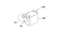
- the capacitor C60 shown in FIG. 23 is also provided with an overhanging portion 601 for fixing outside the housing 600, so that a mounting region (space) D3 is required on the mounting side of the electronic device or the like at the time of mounting. become.
- the present invention has been made in view of the above-described problems, and can reduce the size of the entire capacitor including the housing, and can improve the heat dissipation by the capacitor itself, thereby improving the degree of freedom in designing the mounted device.
- An object of the present invention is to provide a capacitor structure that can be used.
- a first aspect of a capacitor structure according to the present invention includes a plurality of winding capacitors, a housing that houses the plurality of winding capacitors, and the plurality of winding capacitors.
- the capacitor body is fixed to the object to be fixed by inserting the fastener into at least one of a gap generated between the outer peripheral surfaces or a gap generated between the outer peripheral surface of each winding capacitor and the inner wall of the housing.
- the fastener in the capacitor structure according to the first aspect, includes a metal cylindrical body inserted into at least one of the gaps, and the cylinder from the outside of the casing.
- the gist of the present invention is that it is composed of a fixing bolt that is inserted into the body and screwed into the fixing object.
- the fastener is provided with a heat conduction plate disposed so as to contact an outer peripheral surface of each of the winding capacitors arranged side by side.
- the gist of the present invention is that the heat conducting plate is thermally joined to the metallic cylindrical body.
- a cross-sectional shape of the cylindrical body is similar to a planar view shape of the gap.
- the gist is that the outer wall surface is configured to come into contact with the outer peripheral surface of the wound capacitor forming the gap.
- the first electrode plate is disposed on the positive electrode terminal side of each of the winding capacitors, and the first electrode plate is disposed on the negative electrode terminal side of each of the winding capacitors.
- Two electrode plates are respectively disposed, and the metal cylindrical body includes a first metal cylindrical body and a second metal cylindrical body, and the first metal cylindrical body. Is joined to the first electrode plate, and the second metal cylinder is joined to the second electrode plate, and the first metal cylinder and the second metal The gist is that each end portion fastened to the fixed object in the cylindrical body is exposed to the outside from the housing to constitute a terminal.
- the first electrode plate is provided with a first insulating portion that insulates from the second metal cylindrical body
- the gist of the present invention is that the second electrode plate is formed with a second insulating portion that insulates from the first metal cylindrical body.
- a junction between the first metal tubular body and the first electrode plate, or the second metal is that the junction between the cylindrical body and the second electrode plate has a step formed in a direction away from the wound capacitor.
- the joining portion is the first metal cylindrical body or the second metal cylindrical body.
- the overhang portion for fixing does not protrude from the housing. For this reason, the whole capacitor including the housing can be reduced in size. Also, heat can be dissipated through the fastener.
- the fastener is inserted into the cylindrical body from the outside of the housing and screwed into the fixed object through the at least one gap. And fixing bolts.
- the inner wall of the housing can be supported by the metallic cylindrical body, and the housing can be prevented from being deformed by the fastening force when it is fixed to the fixing object by the fixing bolt.
- the fastener is provided with the heat conduction plate disposed so as to be in contact with the outer peripheral surface of each of the wound capacitors arranged side by side. It is thermally joined to the manufactured cylindrical body. For this reason, the heat which generate
- the cross-sectional shape of the cylindrical body is formed to be similar to the planar shape of the gap, and the outer wall surface of the cylindrical body forms the outer periphery of the wound capacitor that forms the gap. It is comprised so that a surface may be contacted. For this reason, the heat which generate
- the first electrode plate and the second electrode plate are arranged in the housing, and the metal cylindrical body has an electrical connection function, so that the bus bar can be used as a bus bar.
- the winding capacitor can be electrically connected without exposing the first electrode plate and the second electrode plate. For this reason, the size of the capacitor including the housing can be reduced.
- the first electrode plate is formed with the first insulating portion that insulates from the second metal cylindrical body, and the second electrode plate has the first metal A second insulating portion is formed to insulate from the manufactured cylindrical body. For this reason, each edge part fastened to fixation object can be exposed outside from a housing
- the junction between the first metal cylindrical body and the first electrode plate, or the junction between the second metal cylindrical body and the second electrode plate. Has a step formed in a direction away from the winding capacitor. For this reason, when soldering the 1st electrode plate and the 2nd electrode plate, and metal cylindrical bodies, the damage by the heat conduction with respect to the capacitor element which a winding type capacitor has can be reduced.
- the edge of the insertion hole of the joint and the end of the metal cylindrical body are joined by solder. For this reason, reliable electrical joining can be performed.
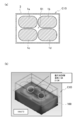
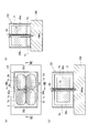
- FIG. 1 is a diagram showing a configuration example of a capacitor structure according to the first embodiment, (a) a sectional view showing a schematic configuration of the capacitor structure, (b) a sectional view taken along line IB-IB, and (c). It is IC-IC line sectional drawing.
- FIG. 2 is a cross-sectional view (a) illustrating a configuration example of a capacitor structure according to a comparative example and an explanatory diagram (b) illustrating a thermal simulation result.
- FIG. 3 is an explanatory diagram illustrating a thermal simulation result of the capacitor structure according to the first embodiment.
- FIG. 4 is a cross-sectional view showing another configuration example of the capacitor structure according to the first embodiment.
- FIG. 5 is a cross-sectional view showing another configuration example of the capacitor structure according to the first embodiment.
- FIG. 6 is a cross-sectional view showing another configuration example of the capacitor structure according to the first embodiment.
- 7A and 7B are diagrams showing a configuration example of the capacitor structure according to the second embodiment.
- FIG. 7A is a sectional view showing a schematic configuration of the capacitor structure
- FIG. 7B is a sectional view taken along the line VIIB-VIIB
- FIG. It is a VIIC-VIIC line sectional view.
- FIG. 8 is an explanatory diagram showing a thermal simulation result of the capacitor structure according to the second embodiment.
- FIG. 9 is a cross-sectional view showing another configuration example of the capacitor structure according to the second embodiment.
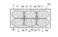
- FIG. 10 is a cross-sectional view illustrating another configuration example of the capacitor structure according to the second embodiment.
- FIG. 11 is a cross-sectional view showing another configuration example of the capacitor structure according to the second embodiment.
- FIG. 12 is a cross-sectional view illustrating a configuration example of the capacitor structure according to the third embodiment.
- FIG. 13 is a cross-sectional view showing another configuration example of the capacitor structure according to the third embodiment.
- FIG. 14 is a cross-sectional view illustrating another configuration example of the capacitor structure according to the third embodiment.
- FIG. 15 is a perspective view showing a configuration example of a capacitor to which the capacitor structure according to the fourth embodiment is applied.
- FIG. 15 is a perspective view showing a configuration example of a capacitor to which the capacitor structure according to the fourth embodiment is applied.
- FIG. 16 is a perspective view showing a configuration example of a heat conducting member including a cylindrical body and a heat conducting plate used in the capacitor structure according to the fourth embodiment.
- FIG. 17 is a perspective view showing a part of the configuration of the capacitor structure according to the fourth embodiment.
- FIG. 18 is a perspective view (a) showing a part of the configuration of the capacitor structure according to the fourth embodiment and a side view (b) in which a part thereof is enlarged.
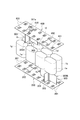
- FIG. 19 is an exploded perspective view showing a capacitor module constituting the capacitor structure according to the fourth embodiment.
- FIG. 20 is a perspective view showing a configuration example of a capacitor module constituting the capacitor structure according to the fourth embodiment.
- FIG. 21 is an explanatory view showing a state in which the capacitor module constituting the capacitor structure according to the fourth embodiment is housed in a housing.
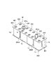
- FIG. 22 is a perspective view showing a capacitor structure according to a comparative example.
- FIG. 23 is a perspective view showing a capacitor structure according to another comparative example.
- Capacitor structure according to the first embodiment A configuration example of the capacitor structure C1 according to the first embodiment will be described with reference to FIGS.
- FIG. 1 is a diagram illustrating a configuration example of a capacitor structure C1 according to the first embodiment.
- FIG. 1A is a cross-sectional view illustrating a schematic configuration of the capacitor structure C1
- FIG. 1C is a sectional view taken along line IB
- FIG. 1C is a sectional view taken along line IC-IC.
- the capacitor structure C1 includes a plurality (four elements in the example shown in FIG. 1) of wound capacitors 1a to 1d made of resin (for example, polyphenylene sulfide resin (PPS: This is a capacitor structure in which a capacitor main body housed in a casing (case) 3 molded with Poly (Phenylene Sulfide Resin) is fixed to a fixing target via a fastener.
- resin for example, polyphenylene sulfide resin (PPS: This is a capacitor structure in which a capacitor main body housed in a casing (case) 3 molded with Poly (Phenylene Sulfide Resin) is fixed to a fixing target via a fastener.
- a fastener is inserted into at least one of the gaps formed between the outer peripheral surfaces 2a to 2d of 1d and the inner wall of the housing 3 (only the gap S1 in the configuration example shown in FIG. 1) to fix the capacitor main body as a fixing target. It is configured to be fixed to a member (for example, a pedestal or a member of various electric devices) 100.
- the entire capacitor including the housing 3 can be reduced in size.
- the fastener is made of a metal (for example, copper or aluminum) inserted through the gap S1 generated between the outer peripheral surfaces 2a to 2d of the wound capacitors 1a to 1d. It is comprised from the cylindrical body 10 and the fixing volt
- a metal for example, copper or aluminum
- the inner wall of the housing 3 can be supported by the metallic cylindrical body 10, and the housing 3 is prevented from being deformed by a fastening force when it is fixed to the fixing object 100 by the fixing bolt 20. can do.
- FIG. 2A is a cross-sectional view showing a configuration example of a capacitor structure C10 according to a comparative example
- FIG. 2B is an explanatory view showing the thermal simulation result
- FIG. 3 is a capacitor structure C1 according to the first embodiment. It is explanatory drawing which shows the thermal simulation result.
- the metal cylindrical body 10 is not provided in the gap S1 generated between the outer peripheral surfaces 2a to 2d of the wound capacitors 1a to 1d. It has a configuration.
- the temperature rise in the maximum heat generating portion was 21.0 K, and the average temperature was 106.0 ° C.
- the temperature rise in the maximum heat generating portion was 20.1K, and the average temperature was 105.1 ° C.
- the capacitor structure C1 according to the present embodiment shows a slightly lower result in both the temperature rise and the average temperature of the maximum heat generating portion. This is because in the capacitor structure C1 according to the present embodiment, the inside of the housing 3 is provided through the metal cylindrical body 10 provided in the gap S1 generated between the outer peripheral surfaces 2a to 2d of the wound capacitors 1a to 1d. This is probably because part of the heat is radiated to the outside.
- FIG. 4 is a cross-sectional view showing another configuration example of the capacitor structure according to the first embodiment.
- the metallic cylindrical body 10 is also provided in the gaps S2 to S5 generated in the above.
- the metallic cylindrical body 10 is also provided in the gaps S6 and S7 generated between the two.
- the housing 3 can be reliably fixed by the fixing object 100 and, of course, the heat in the housing 3 can be radiated more efficiently via the plurality of metal cylindrical bodies 10. It becomes.
- FIG 5 and 6 are cross-sectional views showing other examples of the structure of the capacitor structure according to the first embodiment.
- the metallic cylindrical body 10 is provided in the two gaps S1 and S10 generated between the outer peripheral surfaces 2a to 2f of the wound capacitors 1a to 1f.
- a metallic cylindrical body 10 is provided in two gaps S1 and S11 generated between the outer peripheral surfaces 2a to 2f of the wound capacitors 1a to 1f.
- the housing 3 can be reliably fixed by the fixing object 100, and the heat in the housing 3 can be radiated more efficiently via the plurality of metal tubular bodies 10. .
- the size of the housing 3 and the number of elements of the wound capacitor accommodated in the housing 3 are not limited to 4 elements or 6 elements.
- the winding capacitors 1a to 1f are shown as having an elliptical shape in plan view.
- the visual shape may be a circular shape or other shapes.
- Capacitor structure according to the second embodiment A configuration example of the capacitor structure C2 according to the second embodiment will be described with reference to FIGS.
- FIG. 7 is a diagram showing a configuration example of the capacitor structure C2 according to the second embodiment.
- FIG. 7A is a cross-sectional view showing a schematic configuration of the capacitor structure C2
- FIG. 7C is a sectional view taken along the line VIIB
- FIG. 7C is a sectional view taken along the line VIIC-VIIC.
- the capacitor structure C2 according to the second embodiment is different from the capacitor structure C1 according to the first embodiment in that the capacitor structure C2 contacts the outer peripheral surfaces 2a to 2d of the wound capacitors 1a to 1d arranged in parallel.
- the heat conducting plates 30a to 30d are provided at the positions.
- the heat conductive plates 30a to 30d are formed of, for example, a metal plate such as copper or aluminum having a thickness of about 2 mm, and are thermally bonded to the metallic cylindrical body 10.
- the method for producing the heat conductive plates 30a to 30d and the cylindrical body 10 is not particularly limited, but can be integrally formed by, for example, extrusion molding.
- the heat generated in the winding type capacitors 1a to 1d can be efficiently released to the outside of the housing 3 through the heat conductive plates 30a to 30d, the cylindrical body 10, and the fixing bolt 20. it can.
- FIG. 8 is an explanatory diagram showing a thermal simulation result of the capacitor structure C2 according to the second embodiment.
- the temperature rise in the maximum heat generating portion was 17.6K, and the average temperature was 102.6 ° C.
- the temperature rise in the maximum heat generating portion was 20.1 K, and the average temperature was 105.1 ° C.
- the capacitor structure C2 according to the present embodiment shows lower results in both the temperature rise and the average temperature of the maximum heat generating portion.
- the heat conduction plates 30a to 30d provided in the capacitor structure C2 according to the present embodiment absorb the heat of each of the winding type capacitors 1a to 1d and transfer it to the metal cylindrical body 10, This is considered to be due to efficient discharge to the outside of the housing 3 through the tubular body 10 and the fixing bolt 20.
- 9 to 11 are cross-sectional views showing other examples of the structure of the capacitor structure according to the second embodiment.
- a metal cylindrical body 10 is also provided in the gaps S6 to S9 generated between the outer peripheral surfaces 2a to 2d of the winding capacitors 1a to 1d and the inner wall of the housing 3,
- the metallic cylindrical bodies 10 are thermally connected to each other by the heat conductive plates 30a to 30d.
- the metal cylinders 10 are provided in the gaps S1 and S10, and the metal cylinders 10 are thermally connected to each other by the heat conductive plates 30a to 30g.
- each of the winding type capacitors 1a to 1f is absorbed by the heat conductive plates 30a to 30g, and the heat is transferred to the two metal cylindrical bodies 10, so that each cylindrical body 10 and each fixing bolt 20 are transferred.
- the heat can be efficiently radiated to the outside of the housing 3 via the.
- the metal cylinders 10 are provided in the gaps S1 and S11, and the metal cylinders 10 are thermally connected to each other by the heat conductive plates 30a to 30g.
- each of the winding type capacitors 1a to 1f is absorbed by the heat conductive plates 30a to 30g, and the heat is transferred to the two metal cylindrical bodies 10, so that each cylindrical body 10 and each fixing bolt 20 are transferred.
- the heat can be efficiently radiated to the outside of the housing 3 via the.
- the size of the housing 3 and the number of elements of the wound capacitor accommodated in the housing 3 are not limited to 4 elements or 6 elements.
- the winding capacitors 1a to 1f have been shown to have elliptical shapes in plan view.
- the visual shape may be a circular shape or other shapes.
- Capacitor structure according to the third embodiment A configuration example of the capacitor structures C3a to C3d according to the third embodiment will be described with reference to FIGS.
- FIGS. 12 to 14 are cross-sectional views showing configuration examples of capacitor structures C3a to C3d according to the third embodiment.
- the cross-sectional shapes of the cylindrical bodies 50 to 90 are similar to the plan view shapes of the gaps S1 to S11. ing.
- the outer wall surfaces of the cylindrical bodies 50 to 90 are configured to come into contact with the outer peripheral surfaces 2a to 2f of the wound capacitors 1a to 1f forming the gaps S1 to S11.
- the cross-sectional shapes of the cylindrical bodies 50 to 90 are similar to the planar view shapes of the gaps S1 to S11. Since the outer wall surfaces 50 to 90 are in contact with the outer peripheral surfaces 2a to 2f of the winding capacitors 1a to 1f forming the gaps S1 to S11, the heat generated by the winding capacitors 1a to 1f is caused by the outside of the casing. It can be released efficiently.
- Capacitor structure according to the fourth embodiment A configuration example of the capacitor structure C4 according to the fourth embodiment will be described with reference to FIGS.
- FIG. 15 is a perspective view showing a configuration example of a capacitor to which the capacitor structure C4 according to the fourth embodiment is applied.
- the capacitor structure C4 is configured by housing a capacitor module M described later in a resin casing 470 and filling an insulating resin (for example, epoxy resin) 480.
- an insulating resin for example, epoxy resin
- one end portions 301a of the first metal cylindrical body 301A and the second metal cylindrical body 301B constituting the terminals E1 and E2 are exposed.
- FIG. 16 is a perspective view showing a configuration example of a heat conducting member 300A (300B) including a cylindrical body 301A (301B) and a heat conducting plate 303 used in the capacitor structure C4 according to the fourth embodiment. .
- the heat conducting member 300 ⁇ / b> A (300 ⁇ / b> B) has a shape in which a heat conducting plate 303 is joined to each side surface of a prismatic cylindrical body 301 ⁇ / b> A (301 ⁇ / b> B).
- heat conductive member 300A (300B) is not particularly limited, but can be integrally formed by, for example, extrusion molding of an aluminum material or the like.
- cylindrical body 301A (301B) is formed with an insertion hole 302 through which a fixing bolt can be inserted.
- FIG. 17 is a perspective view showing a part of the configuration of the capacitor structure C4 according to the fourth embodiment.
- the other end 301 b of the second metal cylindrical body 301 ⁇ / b> B is joined to one surface side of the second electrode plate 200.
- the second electrode plate 200 is formed by punching a copper plate or the like, for example, and functions as a bus bar that electrically connects a plurality of wound capacitors 1a to 1h as will be described later.
- the second electrode plate 200 is formed with a plurality of joints 201 to be soldered to lower terminals (for example, negative terminals) of the winding type capacitors 1a to 1h. Moreover, the insertion part 202 which penetrates the other end part 301b of 301 A of 1st cylindrical bodies of the other heat conductive member 300A is formed.
- FIG. 18A is a perspective view showing a part of the structure of the capacitor structure C4 according to the fourth embodiment, and FIG. 18B is an enlarged side view of the part.
- one end 301a of the first cylindrical body 301A of the heat conducting member 300A is joined to one surface side of the first electrode plate 400.
- the first electrode plate 400 is formed by punching a copper plate or the like, for example, and functions as a bus bar that electrically connects a plurality of wound capacitors 1a to 1h as described later.
- the first electrode plate 400 is formed with a plurality of joint portions 401 that are joined to upper terminals (for example, positive terminals) of the winding type capacitors 1a to 1h (see FIG. 18A). Moreover, the insertion part 402 which penetrates the one end part 301a of the 2nd cylindrical body 301B of the other heat conductive member 300B is formed.
- the joining portion 410 of the first electrode plate 400 is formed with a height of, for example, about several millimeters in a direction away from the winding capacitors 1a to 1h (upward in FIGS. 18A and 18B).
- a similar step may be provided at the joint 205 of the second electrode plate 200.
- One end 301a of the first cylindrical body 301A of the heat conducting member 300A is joined to the first electrode plate 400 by solder S through the insertion hole 410a of the joint 410. Thereby, reliable electrical joining can be performed.
- soldering of the one end portion 301a of the first cylindrical body 301A of the heat conducting member 300A and the joint portion 410 can be performed after the first electrode plate 400 is placed on the winding type capacitors 1a to 1h. .
- the level difference H is formed at the joint portion 410 of the first electrode plate 400, when the first electrode plate 400 and the first cylindrical body 301A are soldered, the winding capacitors 1a to 1a. Damage due to heat conduction to the capacitor element of 1h can be reduced.
- FIG. 19 is an exploded perspective view of the capacitor module M constituting the capacitor structure C4 according to the fourth embodiment.
- the second electrode plate 200 is disposed on the lower surface side of the winding capacitors 1a to 1h, and the upper surfaces of the winding capacitors 1a to 1h.
- the first electrode plates 400 are assembled so as to abut each other.
- the second electrode plate 200 is provided with a heat conductive member 300B
- the first electrode plate 400 is provided with a heat conductive member 300A.
- the heat conductive plate 303 provided in each of the heat conductive members 300A and 300B is brought into contact with the side surfaces of the wound capacitors 1a to 1h.
- the soldering between the one end portion 301a of the first cylindrical body 301A of the heat conducting member 300A and the joint portion 410 is performed after the first electrode plate 400 is placed on the wound capacitors 1a to 1h. You may make it perform.
- FIG. 20 is a perspective view showing a configuration example of the capacitor module M after assembly that constitutes the capacitor structure C4 according to the fourth embodiment.
- the first electrode plate 400 and the second electrode plate 200 are assembled to the winding type capacitors 1a to 1h.
- this insertion part 402 comprises the 1st insulating part which insulates the 1st electrode plate 400 and the 2nd metal cylindrical body 301B.
- the other end portion 301b of the heat conducting member 300B is exposed to the lower surface side through the insertion portion 202 (see FIG. 19 and the like) formed in the second electrode plate 200.
- the insertion portion 202 constitutes a second insulating portion that insulates the second electrode plate 200 and the first metal cylindrical body 301A.
- each joint portion 401 included in the first electrode plate 400 is joined to the terminal surface on the upper side of the wound capacitors 1a to 1h by the joining material 450.
- each joint 201 of the second electrode plate 200 is also joined to the lower terminal surface of the winding type capacitors 1a to 1h by the joining material.
- FIG. 21 is an explanatory diagram showing a state in which the capacitor module M constituting the capacitor structure C4 according to the fourth embodiment is housed in the housing 470.
- the housing 470 is formed of an insulating resin, and the upper surface side is open.
- the capacitor module M assembled as shown in FIG. 20 is lowered and accommodated in the housing 470 from the opened upper surface side with the second electrode plate 200 downward.
- the bottom surface 470a of the housing 470 is provided with a convex portion 471 that engages with the second electrode plate 200 of the capacitor module M to perform positioning.
- the bottom surface 470a of the housing 470 is provided with an insertion hole 472 that exposes the other end portion 301b of the heat conducting members 300A and 300B of the capacitor module M to the outside.
- the resin filled in the housing 470 leaks into the gap between the insertion hole 472 and the other end portion 301b of the heat conducting members 300A and 300B as described later. There is a seal so that there is no.
- the gap between the inner wall of the housing 470 and the capacitor module M and the upper surface side of the capacitor module M are filled with an insulating resin (for example, epoxy resin) 480, and the capacitor structure C4 as shown in FIG. Is configured.
- an insulating resin for example, epoxy resin
- one end portion 301a of the first metal cylindrical body 301A and the second metal cylindrical body 301B constituting the terminals E1 and E2 are exposed on the upper surface of the resin 480. Is configured to do.
- the capacitor having the capacitor structure C4 can be connected to various devices via the terminals E1 and E2.
- the first electrode plate 400 and the second electrode plate 200 are arranged in the housing 470, and the heat conducting members 300A and 300B are made of metal.
- the electric power of the winding capacitors 1a to 1h can be obtained without exposing the first electrode plate 400 and the second electrode plate 200 as a bus bar from the housing 470. Connection can be made.
- the entire capacitor including the housing 470 can be downsized.
- inductance can be reduced, and electrical characteristics can be improved.
- the structure of the capacitor structure C4 according to the fourth embodiment has a step in the direction away from the winding type capacitors 1a to 1h in at least one of the first electrode plate and the second electrode plate. H. For this reason, when soldering the first electrode plate 400 and the second electrode plate 200 and the metal cylindrical bodies 301A and 301B, damage due to heat conduction to the capacitor elements included in the wound capacitors 1a to 1h is reduced. can do.
- edge part of the insertion hole 410a which the joint part 410 has, and the one end part 301a of the 1st metal cylinder 301A are joined by solder
- first metal cylindrical body 301A and second metal cylindrical body 301B when one end 301a of first metal cylindrical body 301A and second metal cylindrical body 301B is exposed from the upper surface of resin 480 to form terminals E1 and E2. showed that.
- the present invention is not limited thereto, and the terminal E1, from the side surface or bottom surface of the housing 470 through the conductive plate or the like from one end 301a of the first metal cylindrical body 301A and the second metal cylindrical body 301B. You may comprise so that E2 may be exposed.
- the fixing overhang does not protrude from the housing. For this reason, the whole capacitor including the housing can be reduced in size. Also, heat can be dissipated through the fastener.
Landscapes
- Engineering & Computer Science (AREA)
- Power Engineering (AREA)
- Microelectronics & Electronic Packaging (AREA)
- Manufacturing & Machinery (AREA)
- Fixed Capacitors And Capacitor Manufacturing Machines (AREA)
Abstract
複数の巻回型コンデンサ(1a~1d)を筐体(3)に収納したコンデンサ本体を締結具(筒状体(10)、固定用ボルト(20))を介して固定対象(100)に固定するコンデンサ構造であって、巻回型コンデンサを筐体の底部上に並設した状態で、当該巻回型コンデンサ同士の外周面(2a~2d)間に生じる隙間(S1)または各巻回型コンデンサの外周面と筐体の内壁との間に生じる隙間(S2~S5)の少なくとも一つに、締結具を挿通させてコンデンサ本体を固定対象に固定するように構成されている。
Description
本発明は、複数の巻回型コンデンサを筐体に収納したコンデンサ構造に関する。
従来から、車載用インバータ等に用いる平滑コンデンサとしては、周波数応答性の良さと、故障態様の把握が容易な点を考慮して、一般的にフィルムコンデンサが使われている。
フィルムコンデンサには、フィルム積層型とフィルム巻回型があるが、車載用では比較的低コストな巻回型コンデンサを使用するのが主流である。
このようなコンデンサ構造に係る技術は提案されている(特許文献1参照)。
特許文献1に係る従来技術では、コンデンサケースの両端にはレギュレータケースの貫通穴と一致する貫通穴が設けられている。また一対のターミナルが電極に接続されたコンデンサ素子を収納する収納部が形成されている。
このような従来の巻回型コンデンサでは、車両等に搭載される電子機器などに固定するために、ブラケットなどの固定部品を用いたり、あるいは巻回型コンデンサを収容したコンデンサ本体の樹脂ケースの外部に固定用の座面や補強構造等を設けてボルト等で固定するのが一般的であった。
また、コンデンサ自体を熱伝導率が高い金属部材等に配置するなどして、コンデンサの放熱対策を図っていた。
しかしながら、上記のような従来技術では、図22、図23に示すように、ケースから固定用の張出し部(領域D1~D3参照)が突出していた。そして、このことが車載用インバータ等の装置やシステム等の小型化を阻む要因の一つとなるという問題があった。
即ち、図22に示すコンデンサC50では、筐体500の外部に固定用の張出し部501a、501bが設けられているため、取付時において車載用インバータ等の取付側に取付用領域(スペース)D1、D2が必要になる。このため車載用インバータ等の小型化を妨げてしまう。
また、図23に示すコンデンサC60でも同様に、筐体600の外部に固定用の張出し部601が設けられているため、取付時において電子機器等の取付側に取付用領域(スペース)D3が必要になる。
また、従来技術では、コンデンサ自体の放熱性を高めるために金属部材等に配置する必要があった。このため、コンデンサの配置位置が制限され、車載用インバータ等の装置やシステムの設計自由度が低下するという難点もあった。
本発明は、上記課題に鑑みてなされたものであり、筐体を含めたコンデンサ全体の小型化を図ることができると共に、コンデンサ自体による放熱性を高めて、搭載機器の設計自由度を向上させることのできるコンデンサ構造を提供することを目的とする。
上記目的を達成するため、本発明に係るコンデンサ構造の第1の態様は、複数の巻回型コンデンサと、前記複数の巻回型コンデンサを収容する筐体と、前記複数の巻回型コンデンサを筐体に収納したコンデンサ本体を固定対象に固定する締結具とを備えるコンデンサ構造であって、前記巻回型コンデンサを前記筐体の底部上に並設した状態で、当該巻回型コンデンサ同士の外周面間に生じる隙間または各巻回型コンデンサの外周面と前記筐体の内壁との間に生じる隙間の少なくとも一つに、前記締結具を挿通させて前記コンデンサ本体を前記固定対象に固定するように構成されていることを要旨とする。
本発明に係る第2の態様は、第1の態様に係るコンデンサ構造において、前記締結具は、少なくとも1つの前記隙間に挿通される金属製の筒状体と、前記筐体の外部から前記筒状体に挿通されて前記固定対象に螺合される固定用ボルトとから構成されることを要旨とする。
本発明に係る第3の態様は、第2の態様に係るコンデンサ構造において、前記締結具は、並設される前記各巻回型コンデンサの外周面に接触するように配置される熱伝導板が設けられており、前記熱伝導板は、前記金属製の筒状体に熱的に接合されていることを要旨とする。
本発明に係る第4の態様は、第2または第3の態様に係るコンデンサ構造において、前記筒状体の断面形状は、前記隙間の平面視形状と相似形に形成され、前記筒状体の外壁面が、前記隙間を形成する前記巻回型コンデンサの外周面と接触するように構成されていることを要旨とする。
本発明に係る第5の態様は、第2から第4の態様に係るコンデンサ構造において、前記各巻回型コンデンサの正極端子側に第1電極板が、前記各巻回型コンデンサの負極端子側に第2電極板が、それぞれ配置され、前記金属製の筒状体は、第1の金属製の筒状体と第2の金属製の筒状体を含み、前記第1の金属製の筒状体は、前記第1電極板と接合され、前記第2の金属製の筒状体は、前記第2電極板と接合され、前記第1の金属製の筒状体および前記第2の金属製の筒状体において前記固定対象に締結されるそれぞれの端部は、前記筐体から外部に露出されて端子を構成することを要旨とする。
本発明に係る第6の態様は、第5の態様に係るコンデンサ構造において、前記第1電極板には、前記第2の金属製の筒状体と絶縁する第1絶縁部が形成され、前記第2電極板には、前記第1の金属製の筒状体と絶縁する第2絶縁部が形成されていることを要旨とする。
本発明に係る第7の態様は、第5または第6の態様に係るコンデンサ構造において、前記第1の金属製の筒状体と前記第1電極板との接合部、または前記第2の金属製の筒状体と前記第2電極板との接合部は、前記巻回型コンデンサから離間する方向に形成される段差を有していることを要旨とする。
本発明に係る第8の態様は、第5から第7の態様に係るコンデンサ構造において、前記接合部は、前記第1の金属製の筒状体または前記第2の金属製の筒状体の端部が挿通される挿通孔を有し、該挿通孔の縁部と前記第1の金属製の筒状体または前記第2の金属製の筒状体の当該端部とはハンダで接合されていることを要旨とする。
第1の態様に係るコンデンサ構造によれば、筐体から固定用の張出し部が突出することがない。このため、筐体を含めたコンデンサ全体を小型化することができる。また、締結具を介した放熱を行うことができる。
第2の態様に係るコンデンサ構造によれば、締結具は、少なくとも1つの隙間に挿通される金属製の筒状体と、筐体の外部から筒状体に挿通されて固定対象に螺合される固定用ボルトとから構成されている。このため、金属製の筒状体により、筐体の内壁を支承することができ、固定用ボルトにより固定対象に固定する際に、筐体が締結力により変形する事態を防止することができる。
第3の態様に係るコンデンサ構造によれば、締結具は、並設される各巻回型コンデンサの外周面に接触するように配置される熱伝導板が設けられており、熱伝導板は、金属製の筒状体に熱的に接合されている。このため、巻回型コンデンサで発生する熱を熱伝導板、筒状体および固定用ボルトを介して筐体の外部に効率的に放出することができる。
第4の態様に係るコンデンサ構造によれば、筒状体の断面形状は、隙間の平面視形状と相似形に形成され、筒状体の外壁面が、隙間を形成する巻回型コンデンサの外周面と接触するように構成されている。このため、巻回型コンデンサで発生する熱を筐体の外部により効率的に放出することができる。
第5の態様に係るコンデンサ構造によれば、筐体内に第1電極板と第2電極板を配置し、金属製の筒状体に電気的接続機能を持たせることにより、筐体からバスバとしての第1電極板と第2電極板を露出させることなく巻回型コンデンサの電気的接続を行うことができる。このため、筐体を含めたコンデンサの小型化を図ることができる。
第6の態様に係るコンデンサ構造によれば、第1電極板には、第2の金属製の筒状体と絶縁する第1絶縁部が形成され、第2電極板には、第1の金属製の筒状体と絶縁する第2絶縁部が形成されている。このため、短絡することなく、固定対象に締結されるそれぞれの端部を筐体から外部に露出させることができる。
第7の態様に係るコンデンサ構造によれば、第1の金属製の筒状体と第1電極板との接合部、または第2の金属製の筒状体と第2電極板との接合部は、巻回型コンデンサから離間する方向に形成される段差を有している。このため、第1電極板および第2電極板と金属製の筒状体とをハンダ付けする際に、巻回型コンデンサが有するコンデンサ素子に対する熱伝導によるダメージを低減することができる。
第8の態様に係るコンデンサ構造によれば、接合部が有する挿通孔の縁部と金属製の筒状体の端部とはハンダで接合される。このため、確実な電気的接合を行うことができる。
以下、本発明の一例としての実施の形態を図面に基づいて詳細に説明する。ここで、添付図面において同一の部材には同一の符号を付しており、また、重複した説明は省略されている。なお、本発明は以下に示す実施の形態に限定されるものではない。
(第1の実施の形態に係るコンデンサ構造)
図1から図6を参照して、第1の実施の形態に係るコンデンサ構造C1の構成例について説明する。
図1から図6を参照して、第1の実施の形態に係るコンデンサ構造C1の構成例について説明する。
図1は、第1の実施の形態に係るコンデンサ構造C1の構成例を示す図であり、図1(a)はそのコンデンサ構造C1の概略構成を示す断面図、図1(b)はIB-IB線断面図、図1(c)はIC-IC線断面図である。
図1に示すように、第1の実施の形態に係るコンデンサ構造C1は、複数(図1に示す例では4素子)の巻回型コンデンサ1a~1dを樹脂(例えば、ポリフェニレンサルファイド樹脂(PPS:Poly Phenylene Sulfide Resin))で成形された筐体(ケース)3に収納したコンデンサ本体を、締結具を介して固定対象に固定するコンデンサ構造である。
そして、巻回型コンデンサ1a~1dを筐体3の底部上に並設した状態で、当該巻回型コンデンサ1a~1d同士の外周面2a~2d間に生じる隙間S1または各巻回型コンデンサ1a~1dの外周面2a~2dと筐体3の内壁との間に生じる隙間の少なくとも一つ(図1に示す構成例では隙間S1のみ)に、締結具を挿通させてコンデンサ本体を固定対象としての部材(例えば、台座や各種電気機器の部材等)100に固定するように構成されている。
これにより、従来のように筐体3から固定用の張出し部が突出することがないので、筐体3を含めたコンデンサ全体を小型化することができる。
本実施の形態に係るコンデンサ構造C1では、前記締結具は、巻回型コンデンサ1a~1d同士の外周面2a~2d間に生じる隙間S1に挿通される金属製(例えば、銅やアルミニウム等)の筒状体10と、筐体3の外部から筒状体10に挿通されて固定対象としての部材100のボルト孔100aに螺合される固定用ボルト20とから構成されている。
これにより、金属製の筒状体10により、筐体3の内壁を支承することができ、固定用ボルト20により固定対象100に固定する際に、筐体3が締結力により変形する事態を防止することができる。
ここで、図2および図3を参照して、比較例に係るコンデンサ構造C10と、本実施の形態に係るコンデンサ構造C1との放熱性について比較する。
図2(a)は比較例に係るコンデンサ構造C10の構成例を示す断面図、図2(b)はその熱シミュレーション結果を示す説明図、図3は第1の実施の形態に係るコンデンサ構造C1の熱シミュレーション結果を示す説明図である。
図2(a)に示すように、比較例に係るコンデンサ構造C10では、巻回型コンデンサ1a~1d同士の外周面2a~2d間に生じる隙間S1には金属製の筒状体10を設けない構成となっている。この場合の熱シミュレーションでは、最大発熱部における温度上昇は21.0K、平均温度は106.0℃であった。
一方、本実施の形態に係るコンデンサ構造C1の熱シミュレーションでは、最大発熱部における温度上昇は20.1K、平均温度は105.1℃であった。
このように、比較例に係るコンデンサ構造C10に比して、本実施の形態に係るコンデンサ構造C1の方が最大発熱部の温度上昇および平均温度の双方で若干低い結果を示している。これは、本実施の形態に係るコンデンサ構造C1では、巻回型コンデンサ1a~1d同士の外周面2a~2d間に生じる隙間S1に設けた金属製の筒状体10を介して筐体3内の熱の一部が外部に放熱されるためであると考えられる。
図4は、第1の実施の形態に係るコンデンサ構造の他の構成例を示す断面図である。
図4(a)、(b)に示すコンデンサ構造C1a、C1bの基本構成は、図1に示すコンデンサ構造C1と同様であるので、同一符号を付して重複した説明は割愛する。
コンデンサ構造C1aでは、巻回型コンデンサ1a~1d同士の外周面2a~2d間に生じる隙間S1に加えて、各巻回型コンデンサ1a~1dの外周面2a~2dと筐体3の内壁との間に生じる隙間S2~S5にも金属製の筒状体10を設けている。
また、コンデンサ構造C1bでは、巻回型コンデンサ1a~1d同士の外周面2a~2d間に生じる隙間S1に加えて、各巻回型コンデンサ1a~1dの外周面2a~2dと筐体3の内壁との間に生じる隙間S6、S7にも金属製の筒状体10を設けている。
これにより、筐体3を固定対象100により確実に固定することができるのは勿論、複数の金属製の筒状体10を介して筐体3内の熱をより効率的に放熱することが可能となる。
図5および図6は、第1の実施の形態に係るコンデンサ構造の他の構成例を示す断面図である。
図5および図6に示すコンデンサ構造C1c、C1dの基本構成は、図1に示すコンデンサ構造C1と同様であるので、同一符号を付して重複した説明は割愛する。
図5に示すコンデンサ構造C1cでは、図1(a)に示すコンデンサ構造C1aについて、筐体3を平面視で横方向に拡大すると共に、収容する巻回型コンデンサを4素子から6素子(1a~1f)に増やしている。そして、巻回型コンデンサ1a~1f同士の外周面2a~2f間に生じる2箇所の隙間S1、S10に金属製の筒状体10を設けている。
図6に示すコンデンサ構造C1dでは、図1(a)に示すコンデンサ構造C1aについて、筐体3を平面視で縦方向に拡大すると共に、収容する巻回型コンデンサを4素子から6素子(1a~1f)に増やしている。そして、巻回型コンデンサ1a~1f同士の外周面2a~2f間に生じる2箇所の隙間S1、S11に金属製の筒状体10を設けている。
これにより、筐体3を固定対象100により確実に固定することができると共に、複数の金属製の筒状体10を介して筐体3内の熱をより効率的に放熱することが可能となる。
なお、筐体3の大きさや、その筐体3に収容される巻回型コンデンサの素子数は、4素子や6素子には限定されない。
また、本実施の形態に係るコンデンサ構造C1、C1a~C1dでは、巻回型コンデンサ1a~1fとして平面視の形状が楕円形状のものを用いる場合を示したが、これには限定されず、平面視の形状が円形状やその他の形状を呈するものであってもよい。
(第2の実施の形態に係るコンデンサ構造)
図7から図11を参照して、第2の実施の形態に係るコンデンサ構造C2の構成例について説明する。
図7から図11を参照して、第2の実施の形態に係るコンデンサ構造C2の構成例について説明する。
図7は、第2の実施の形態に係るコンデンサ構造C2の構成例を示す図であり、図7(a)はそのコンデンサ構造C2の概略構成を示す断面図、図7(b)はVIIB-VIIB線断面図、図7(c)はVIIC-VIIC線断面図である。
なお、第1の実施の形態に係るコンデンサ構造C1と同様の構成については、同一符号を付して重複した説明は割愛する。
第2の実施の形態に係るコンデンサ構造C2が、第1の実施の形態に係るコンデンサ構造C1と異なる点は、並設される各巻回型コンデンサ1a~1dの外周面2a~2dに接触するように配置される熱伝導板30a~30dが設けられている点である。
熱伝導板30a~30dは、例えば厚さ2mm程度の銅やアルミニウム等の金属板などで形成され、金属製の筒状体10に熱的に接合されている。
熱伝導板30a~30dおよび筒状体10の作成方法は、特には限定されないが、例えば押し出し成形により、一体的に形成することができる。
このような構造により、巻回型コンデンサ1a~1dで発生する熱を熱伝導板30a~30d、筒状体10および固定用ボルト20を介して筐体3の外部に効率的に放出することができる。
ここで、図8は、第2の実施の形態に係るコンデンサ構造C2の熱シミュレーション結果を示す説明図である。
図8に示すように、コンデンサ構造C2では、最大発熱部における温度上昇は17.6K、平均温度は102.6℃であった。
また、前出の図3に示す第1の実施の形態に係るコンデンサ構造C1の熱シミュレーションでは、最大発熱部における温度上昇は20.1K、平均温度は105.1℃であった。
このように、第1の実施の形態に係るコンデンサ構造C1に比して、本実施の形態に係るコンデンサ構造C2の方が最大発熱部の温度上昇および平均温度の双方で低い結果を示している。これは、本実施の形態に係るコンデンサ構造C2において設けられた熱伝導板30a~30dによって、各巻回型コンデンサ1a~1dの熱が吸熱されると共に金属製の筒状体10に伝熱され、筒状体10および固定用ボルト20を介して筐体3の外部に効率的に放出されるためであると考えられる。
図9~図11は、第2の実施の形態に係るコンデンサ構造の他の構成例を示す断面図である。
図9~図11に示すコンデンサ構造C2a~C2cの基本構成は、図1~図6に示すコンデンサ構造C1等と同様であるので、同一符号を付して重複した説明は割愛する。
図9に示すコンデンサ構造C2aでは、各巻回型コンデンサ1a~1dの外周面2a~2dと筐体3の内壁との間に生じる隙間S6~S9にも金属製の筒状体10を設けると共に、熱伝導板30a~30dによって金属製の筒状体10同士を熱的に連結している。
これにより、各巻回型コンデンサ1a~1dの熱を熱伝導板30a~30dで吸熱すると共に、複数の金属製の筒状体10に伝熱され、各筒状体10および各固定用ボルト20を介して筐体3の外部により効率的に放熱することができる。
図10に示すコンデンサ構造C2bでは、隙間S1、S10に金属製の筒状体10を設けると共に、熱伝導板30a~30gによって金属製の筒状体10同士を熱的に連結している。
これにより、各巻回型コンデンサ1a~1fの熱を熱伝導板30a~30gで吸熱すると共に、2本の金属製の筒状体10に伝熱され、各筒状体10および各固定用ボルト20を介して筐体3の外部により効率的に放熱することができる。
図11に示すコンデンサ構造C2cでは、隙間S1、S11に金属製の筒状体10を設けると共に、熱伝導板30a~30gによって金属製の筒状体10同士を熱的に連結している。
これにより、各巻回型コンデンサ1a~1fの熱を熱伝導板30a~30gで吸熱すると共に、2本の金属製の筒状体10に伝熱され、各筒状体10および各固定用ボルト20を介して筐体3の外部により効率的に放熱することができる。
なお、筐体3の大きさや、その筐体3に収容される巻回型コンデンサの素子数は、4素子や6素子には限定されない。
また、本実施の形態に係るコンデンサ構造C2、C2a~C2cでは、巻回型コンデンサ1a~1fとして平面視の形状が楕円形状のものを用いる場合を示したが、これには限定されず、平面視の形状が円形状やその他の形状を呈するものであってもよい。
(第3の実施の形態に係るコンデンサ構造)
図12から図14を参照して、第3の実施の形態に係るコンデンサ構造C3a~C3dの構成例について説明する。
図12から図14を参照して、第3の実施の形態に係るコンデンサ構造C3a~C3dの構成例について説明する。
図12から図14は、第3の実施の形態に係るコンデンサ構造C3a~C3dの構成例を示す断面図である。
なお、第2の実施の形態に係るコンデンサ構造C2等と同様の構成については、同一符号を付して重複した説明は割愛する。
図12から図14に示すように、第3の実施の形態に係るコンデンサ構造C3a~C3dでは、筒状体50~90の断面形状は、隙間S1~S11の平面視形状と相似形に形成されている。
そして、筒状体50~90の外壁面が、各隙間S1~S11を形成する巻回型コンデンサ1a~1fの外周面2a~2fと接触するように構成されている。
このように、第3の実施の形態に係るコンデンサ構造C3a~C3dによれば、筒状体50~90の断面形状は、隙間S1~S11の平面視形状と相似形に形成され、筒状体50~90の外壁面が、隙間S1~S11を形成する巻回型コンデンサ1a~1fの外周面2a~2fと接触するので、巻回型コンデンサ1a~1fで発生する熱を筐体の外部により効率的に放出することができる。
(第4の実施の形態に係るコンデンサ構造)
図15から図21を参照して、第4の実施の形態に係るコンデンサ構造C4の構成例について説明する。
図15から図21を参照して、第4の実施の形態に係るコンデンサ構造C4の構成例について説明する。
図15は、第4の実施の形態に係るコンデンサ構造C4を適用したコンデンサの構成例を示す斜視図である。
図15に示すように、コンデンサ構造C4は、樹脂製の筐体470内に、後述するコンデンサモジュールMを収容し、絶縁性樹脂(例えば、エポキシ樹脂)480が充填されて構成されている。
なお、樹脂側の上面には、端子E1、E2を構成する第1の金属製の筒状体301Aおよび第2の金属製の筒状体301Bの一端部301aが露出している。
ここで、図16から図21を参照して、コンデンサ構造C4を構成するコンデンサモジュールMの各部の構成等について説明する。
まず、図16は、第4の実施の形態に係るコンデンサ構造C4で用いられる筒状体301A(301B)と熱伝導板303から成る熱伝導部材300A(300B)の構成例を示す斜視図である。
図16に示すように、熱伝導部材300A(300B)は、角柱形の筒状体301A(301B)の各側面に熱伝導板303を接合した形状となっている。
なお、熱伝導部材300A(300B)の製造方法は特には限定されないが、例えばアルミニウム材等の押し出し成形により、一体的に形成することができる。
また、筒状体301A(301B)には、固定用ボルトを挿通可能な挿通孔302が形成されている。
図17は、第4の実施の形態に係るコンデンサ構造C4の構成の一部を示す斜視図である。
図17に示すように、第2の金属製の筒状体301Bの他端部301bは、第2電極板200の一面側に接合されている。
第2電極板200は、例えば銅板等の打ち抜き加工等により構成され、後述するように複数の巻回型コンデンサ1a~1hを電気的に接続するバスバとして機能する。
第2電極板200には、巻回型コンデンサ1a~1hの下部端子(例えば負極端子)にハンダ付けされる複数の接合部201が形成されている。また、他方の熱伝導部材300Aの第1の筒状体301Aの他端部301bを挿通する挿通部202が形成されている。
なお、熱伝導部材300Bの筒状体301Bの他端部301bは、接合部205を介してハンダSによって第2電極板200に電気的に接合されている。
図18(a)は、第4の実施の形態に係るコンデンサ構造C4の構成の一部を示す斜視図、図18(b)はその一部を拡大した側面図である。
図18(a)、(b)に示すように、熱伝導部材300Aの第1の筒状体301Aの一端部301aは、第1電極板400の一面側に接合されている。
第1電極板400は、例えば銅板等の打ち抜き加工等により構成され、後述するように複数の巻回型コンデンサ1a~1hを電気的に接続するバスバとして機能する。
第1電極板400には、巻回型コンデンサ1a~1hの上部端子(例えば正極端子)に接合される複数の接合部401が形成されている(図18(a)参照)。また、他方の熱伝導部材300Bの第2の筒状体301Bの一端部301aを挿通する挿通部402が形成されている。
ここで、第1電極板400の接合部410には、巻回型コンデンサ1a~1hから離間する方向(図18(a)、(b)では上方)に、例えば高さ数ミリ程度で形成される段差Hを有している。なお、第2電極板200の接合部205にも同様の段差を設けるようにしてもよい。
熱伝導部材300Aの第1の筒状体301Aの一端部301aは、接合部410の挿通孔410aを介してハンダSによって第1電極板400と接合されている。これにより、確実な電気的接合を行うことができる。
なお、熱伝導部材300Aの第1の筒状体301Aの一端部301aと接合部410とのハンダ付けは、巻回型コンデンサ1a~1hに第1電極板400を載置した後に行うようにできる。
この場合、第1電極板400の接合部410には段差Hが形成されているので、第1電極板400と第1の筒状体301Aとをハンダ付けする際に、巻回型コンデンサ1a~1hが有するコンデンサ素子に対する熱伝導によるダメージを低減することができる。
図19は、第4の実施の形態に係るコンデンサ構造C4を構成するコンデンサモジュールMの分解斜視図である。
図19に示す構成例では、8個の巻回型コンデンサ1a~1hを整列させ、巻回型コンデンサ1a~1hの下面側には第2電極板200が、巻回型コンデンサ1a~1hの上面側には第1電極板400がそれぞれ当接するように組み付けられる。
図17~図19に示すように、第2電極板200には熱伝導部材300Bが、第1電極板400には熱伝導部材300Aがそれぞれ配置されている。
また、各熱伝導部材300A、300Bが備える熱伝導板303は、巻回型コンデンサ1a~1hの側面に当接される。
なお、上述したように熱伝導部材300Aの第1の筒状体301Aの一端部301aと接合部410とのハンダ付けは、巻回型コンデンサ1a~1hに第1電極板400を載置した後に行うようにしてもよい。
図20は、第4の実施の形態に係るコンデンサ構造C4を構成する組み付け後のコンデンサモジュールMの構成例を示す斜視図である。
図20に示すように、巻回型コンデンサ1a~1hに、第1電極板400および第2電極板200を組み付ける。
この際に、熱伝導部材300Bの一端部301aは、第1電極板400に形成されている挿通部402を通して上面側に露出される。なお、この挿通部402は、第1電極板400と、第2の金属製の筒状体301Bとを絶縁する第1絶縁部を構成している。
また、図20には現れないが、熱伝導部材300Bの他端部301bは、第2電極板200に形成されている挿通部202(図19等参照)を通して下面側に露出される。なお、この挿通部202は、第2電極板200と、第1の金属製の筒状体301Aとを絶縁する第2絶縁部を構成している。
そして、このように組み付けられた状態で、熱伝導部材300Aの第1の筒状体301Aの一端部301aと接合部410とのハンダ付けを行うようにできる。
この際に、第1電極板400の接合部410には段差Hが形成されているので、巻回型コンデンサ1a~1hが有するコンデンサ素子に対する熱伝導によるダメージが低減される。
また、第1電極板400が有する各接合部401は、接合材450により巻回型コンデンサ1a~1hの上側の端子面に接合される。
なお、図には現れないが、第2電極板200が有する各接合部201も、接合材により巻回型コンデンサ1a~1hの下側の端子面に接合される。
図21は、第4の実施の形態に係るコンデンサ構造C4を構成するコンデンサモジュールMを筐体470に収容する状態を示す説明図である。
筐体470は、絶縁性の樹脂で成形され、上面側は開放されている。
そして、開放されている上面側から筐体470内に、図20に示すようにして組み立てられたコンデンサモジュールMを第2電極板200を下方側にして降下させて収容する。
なお、筐体470の底面470aには、コンデンサモジュールMの第2電極板200と係合して位置決めを行う凸部471が設けられている。
また、筐体470の底面470aには、コンデンサモジュールMの熱伝導部材300A、300Bの他端部301bを外部に露出させる挿通孔472が設けられている。
なお、コンデンサモジュールMを筐体470に収容した状態で、挿通孔472と熱伝導部材300A、300Bの他端部301bとの隙間には、後述するように筐体470に充填される樹脂が漏れないようにシールが施される。
そして、筐体470の内壁等とコンデンサモジュールMとの隙間およびコンデンサモジュールMの上面側には、絶縁性の樹脂(例えば、エポキシ樹脂)480が充填されて、図15に示すようなコンデンサ構造C4が構成される。
なお、図15に示すように、樹脂480の上面には、端子E1、E2を構成する第1の金属製の筒状体301Aおよび第2の金属製の筒状体301Bの一端部301aが露出するように構成されている。
これにより、端子E1、E2を介して、コンデンサ構造C4を有するコンデンサを種々の機器に接続することができる。
以上のような構成の第4の実施の形態に係るコンデンサ構造C4によれば、筐体470内に第1電極板400と第2電極板200を配置し、熱伝導部材300A、300Bの金属製の筒状体301A、301Bに電気的接続機能を持たせることにより、筐体470からバスバとしての第1電極板400と第2電極板200を露出させることなく巻回型コンデンサ1a~1hの電気的接続を行うことができる。この構成によって、筐体470を含めたコンデンサ全体の小型化を図ることができる。また、インダクタンスを低減することもでき、電気的特性を向上させることもできる。
また、第4の実施の形態に係るコンデンサ構造C4の構成は、第1電極板および第2電極板の少なくとも一方の接合部410、205に、巻回型コンデンサ1a~1hから離間する方向に段差Hを有している。このため、第1電極板400、第2電極板200と金属製の筒状体301A、301Bとをハンダ付けする際に、巻回型コンデンサ1a~1hが有するコンデンサ素子に対する熱伝導によるダメージを低減することができる。
また、接合部410が有する挿通孔410aの縁部と第1の金属製の筒状体301Aの一端部301aとはハンダで接合されるので、確実な電気的接合を行うことができる。
なお、本実施の形態では、第1の金属製の筒状体301Aおよび第2の金属製の筒状体301Bの一端部301aが樹脂480の上面から露出して端子E1、E2を構成する場合を示した。しかしこれに限らず、第1の金属製の筒状体301Aおよび第2の金属製の筒状体301Bの一端部301aから導電板等を介して、筐体470の側面あるいは底面から端子E1、E2が露出されるように構成してもよい。
以上本発明者によってなされた発明を実施の形態に基づき具体的に説明したが、本明細書で開示された実施の形態はすべての点で例示であって開示された技術に限定されるものではないと考えるべきである。すなわち、本発明の技術的な範囲は、前記の実施の形態における説明に基づいて制限的に解釈されるものでなく、あくまでも特許請求の範囲の記載にしたがって解釈すべきであり、特許請求の範囲の記載技術と均等な技術および特許請求の範囲内でのすべての変更が含まれる。
本出願は、日本国特許出願第2015-010209号(2015年1月22日出願)および日本国特許出願第2015-164866号(2015年8月24日に出願)に基づく優先権を主張しており、この出願の全内容が参照により本願明細書に組み込まれる。
本発明の一態様に係るコンデンサ構造は、筐体から固定用の張出し部が突出することがない。このため、筐体を含めたコンデンサ全体を小型化することができる。また、締結具を介した放熱を行うことができる。
C1、C1~C1d、C2、C2a~C2c、C3a~C3d、C4 コンデンサ構造
S1~S11 隙間
1a~1h 巻回型コンデンサ
2a~2f 外周面
3、470 筐体
10、50、60、70、80、90 筒状体
20 固定用ボルト
30a~30g、303 熱伝導板
100 固定対象
100a ボルト孔
200 第2電極板
201 接合部
202 挿通部(第2絶縁部)
402 挿通部(第1絶縁部)
300A、300B 熱伝導部材
301A 第1の金属製の筒状体
301B 第2の金属製の筒状体
302 挿通孔
301a 一端部
301b 他端部
400 第1電極板
450 接合材
480 樹脂
205、410 接合部
H 段差
E1、E2 端子
M コンデンサモジュール
S ハンダ
S1~S11 隙間
1a~1h 巻回型コンデンサ
2a~2f 外周面
3、470 筐体
10、50、60、70、80、90 筒状体
20 固定用ボルト
30a~30g、303 熱伝導板
100 固定対象
100a ボルト孔
200 第2電極板
201 接合部
202 挿通部(第2絶縁部)
402 挿通部(第1絶縁部)
300A、300B 熱伝導部材
301A 第1の金属製の筒状体
301B 第2の金属製の筒状体
302 挿通孔
301a 一端部
301b 他端部
400 第1電極板
450 接合材
480 樹脂
205、410 接合部
H 段差
E1、E2 端子
M コンデンサモジュール
S ハンダ
Claims (8)
- 複数の巻回型コンデンサと、
前記複数の巻回型コンデンサを収容する筐体と、
前記複数の巻回型コンデンサを筐体に収納したコンデンサ本体を固定対象に固定する締結具とを備えるコンデンサ構造であって、
前記巻回型コンデンサを前記筐体の底部上に並設した状態で、当該巻回型コンデンサ同士の外周面間に生じる隙間または各巻回型コンデンサの外周面と前記筐体の内壁との間に生じる隙間の少なくとも一つに、前記締結具を挿通させて前記コンデンサ本体を前記固定対象に固定するように構成されていることを特徴とするコンデンサ構造。 - 前記締結具は、
少なくとも1つの前記隙間に挿通される金属製の筒状体と、
前記筐体の外部から前記筒状体に挿通されて前記固定対象に螺合される固定用ボルトと
から構成されることを特徴とする請求項1に記載のコンデンサ構造。 - 前記締結具は、
並設される前記各巻回型コンデンサの外周面に接触するように配置される熱伝導板が設けられており、
前記熱伝導板は、前記金属製の筒状体に熱的に接合されていることを特徴とする請求項2に記載のコンデンサ構造。 - 前記筒状体の断面形状は、前記隙間の平面視形状と相似形に形成され、
前記筒状体の外壁面が、前記隙間を形成する前記巻回型コンデンサの外周面と接触するように構成されていることを特徴とする請求項2または請求項3に記載のコンデンサ構造。 - 前記各巻回型コンデンサの正極端子側に第1電極板が、前記各巻回型コンデンサの負極端子側に第2電極板が、それぞれ配置され、
前記金属製の筒状体は、第1の金属製の筒状体と第2の金属製の筒状体を含み、
前記第1の金属製の筒状体は、前記第1電極板と接合され、
前記第2の金属製の筒状体は、前記第2電極板と接合され、
前記第1の金属製の筒状体および前記第2の金属製の筒状体において前記固定対象に締結されるそれぞれの端部は、前記筐体から外部に露出されて端子を構成することを特徴とする請求項2から請求項4の何れか1項に記載のコンデンサ構造。 - 前記第1電極板には、前記第2の金属製の筒状体と絶縁する第1絶縁部が形成され、前記第2電極板には、前記第1の金属製の筒状体と絶縁する第2絶縁部が形成されていることを特徴とする請求項5に記載のコンデンサ構造。
- 前記第1の金属製の筒状体と前記第1電極板との接合部、または前記第2の金属製の筒状体と前記第2電極板との接合部は、前記巻回型コンデンサから離間する方向に形成される段差を有していることを特徴とする請求項5または請求項6に記載のコンデンサ構造。
- 前記接合部は、前記第1の金属製の筒状体または前記第2の金属製の筒状体の端部が挿通される挿通孔を有し、該挿通孔の縁部と前記第1の金属製の筒状体または前記第2の金属製の筒状体の当該端部とはハンダで接合されていることを特徴とする請求項5から請求項7の何れか1項に記載のコンデンサ構造。
Priority Applications (3)
| Application Number | Priority Date | Filing Date | Title |
|---|---|---|---|
| DE112016000457.5T DE112016000457T5 (de) | 2015-01-22 | 2016-01-14 | Kondensator-Struktur |
| US15/545,602 US10062515B2 (en) | 2015-01-22 | 2016-01-14 | Capacitor structure |
| CN201680006885.3A CN107210130A (zh) | 2015-01-22 | 2016-01-14 | 电容器构造 |
Applications Claiming Priority (4)
| Application Number | Priority Date | Filing Date | Title |
|---|---|---|---|
| JP2015010209 | 2015-01-22 | ||
| JP2015-010209 | 2015-01-22 | ||
| JP2015164866A JP6347768B2 (ja) | 2015-01-22 | 2015-08-24 | コンデンサ構造 |
| JP2015-164866 | 2015-08-24 |
Publications (1)
| Publication Number | Publication Date |
|---|---|
| WO2016117441A1 true WO2016117441A1 (ja) | 2016-07-28 |
Family
ID=56416988
Family Applications (1)
| Application Number | Title | Priority Date | Filing Date |
|---|---|---|---|
| PCT/JP2016/050949 Ceased WO2016117441A1 (ja) | 2015-01-22 | 2016-01-14 | コンデンサ構造 |
Country Status (1)
| Country | Link |
|---|---|
| WO (1) | WO2016117441A1 (ja) |
Cited By (4)
| Publication number | Priority date | Publication date | Assignee | Title |
|---|---|---|---|---|
| JP2020064917A (ja) * | 2018-10-16 | 2020-04-23 | 三菱電機株式会社 | 樹脂モールド型コンデンサ、及び電力変換装置 |
| WO2022239069A1 (ja) * | 2021-05-10 | 2022-11-17 | 三菱電機株式会社 | コンデンサユニットおよび電子機器 |
| WO2022270352A1 (ja) * | 2021-06-22 | 2022-12-29 | 三菱電機株式会社 | 回路装置 |
| WO2022270353A1 (ja) * | 2021-06-22 | 2022-12-29 | 三菱電機株式会社 | 回路装置 |
Citations (3)
| Publication number | Priority date | Publication date | Assignee | Title |
|---|---|---|---|---|
| JP2002184374A (ja) * | 2000-12-12 | 2002-06-28 | Honda Motor Co Ltd | 電池パック |
| JP2011009477A (ja) * | 2009-06-26 | 2011-01-13 | Panasonic Corp | 蓄電ユニット |
| US20120081866A1 (en) * | 2010-10-01 | 2012-04-05 | Robert Bosch Gmbh | Brackets for electrical components |
-
2016
- 2016-01-14 WO PCT/JP2016/050949 patent/WO2016117441A1/ja not_active Ceased
Patent Citations (3)
| Publication number | Priority date | Publication date | Assignee | Title |
|---|---|---|---|---|
| JP2002184374A (ja) * | 2000-12-12 | 2002-06-28 | Honda Motor Co Ltd | 電池パック |
| JP2011009477A (ja) * | 2009-06-26 | 2011-01-13 | Panasonic Corp | 蓄電ユニット |
| US20120081866A1 (en) * | 2010-10-01 | 2012-04-05 | Robert Bosch Gmbh | Brackets for electrical components |
Cited By (12)
| Publication number | Priority date | Publication date | Assignee | Title |
|---|---|---|---|---|
| JP2020064917A (ja) * | 2018-10-16 | 2020-04-23 | 三菱電機株式会社 | 樹脂モールド型コンデンサ、及び電力変換装置 |
| WO2022239069A1 (ja) * | 2021-05-10 | 2022-11-17 | 三菱電機株式会社 | コンデンサユニットおよび電子機器 |
| JPWO2022239069A1 (ja) * | 2021-05-10 | 2022-11-17 | ||
| JP7504294B2 (ja) | 2021-05-10 | 2024-06-21 | 三菱電機株式会社 | 電子機器 |
| US12626861B2 (en) | 2021-05-10 | 2026-05-12 | Mitsubishi Electric Corporation | Capacitor unit and electronic device |
| DE112021007634B4 (de) | 2021-05-10 | 2026-07-23 | Mitsubishi Electric Corporation | Elektronische vorrichtung mit einer kondensatoreinheit |
| WO2022270352A1 (ja) * | 2021-06-22 | 2022-12-29 | 三菱電機株式会社 | 回路装置 |
| JPWO2022270352A1 (ja) * | 2021-06-22 | 2022-12-29 | ||
| WO2022270353A1 (ja) * | 2021-06-22 | 2022-12-29 | 三菱電機株式会社 | 回路装置 |
| JPWO2022270353A1 (ja) * | 2021-06-22 | 2022-12-29 | ||
| JP7634674B2 (ja) | 2021-06-22 | 2025-02-21 | 三菱電機株式会社 | 回路装置 |
| JP7634673B2 (ja) | 2021-06-22 | 2025-02-21 | 三菱電機株式会社 | 回路装置 |
Similar Documents
| Publication | Publication Date | Title |
|---|---|---|
| JP6347768B2 (ja) | コンデンサ構造 | |
| JP6488464B2 (ja) | フィルムコンデンサ | |
| JP5799843B2 (ja) | 電力変換装置 | |
| JP6400909B2 (ja) | コンデンサ及びコンデンサの設置方法 | |
| JP2012018904A (ja) | エネルギー貯蔵モジュール | |
| CN108702856A (zh) | 电路构成体 | |
| EP2639802A1 (en) | Electric double-layer capacitor | |
| JP6343249B2 (ja) | コントローラおよびコントローラの製造方法 | |
| CN106716576B (zh) | 电子部件及其制造方法 | |
| JP2011155138A (ja) | コンデンサ | |
| US11456117B2 (en) | Capacitor | |
| JP6184675B2 (ja) | コンデンサ | |
| JP7163542B2 (ja) | コンデンサ | |
| JP5307052B2 (ja) | 車載電気接続箱、及びこれに用いられる回路材、回路ユニット | |
| US12477694B2 (en) | Circuit device | |
| WO2019181109A1 (ja) | コンデンサ | |
| WO2015146584A1 (ja) | 蓄電装置 | |
| CN105934877A (zh) | 用于机动车辆功率电子模块的电容器单元和相应的制造方法 | |
| CN101329945B (zh) | 引脚外接式电解电容器 | |
| JP7425834B2 (ja) | コンデンサ | |
| WO2020153164A1 (ja) | 回路構成体、電気接続箱及び回路構成体の製造方法 | |
| JP2017163809A (ja) | 電動モータ制御装置 | |
| JP6952818B2 (ja) | コンデンサの保持構造および電子機器 | |
| KR101936800B1 (ko) | 케이스 일체형 에너지 저장 장치 | |
| JP2006190911A (ja) | コンデンサ組立体 |
Legal Events
| Date | Code | Title | Description |
|---|---|---|---|
| 121 | Ep: the epo has been informed by wipo that ep was designated in this application |
Ref document number: 16740048 Country of ref document: EP Kind code of ref document: A1 |
|
| DPE1 | Request for preliminary examination filed after expiration of 19th month from priority date (pct application filed from 20040101) | ||
| WWE | Wipo information: entry into national phase |
Ref document number: 15545602 Country of ref document: US |
|
| WWE | Wipo information: entry into national phase |
Ref document number: 112016000457 Country of ref document: DE |
|
| 122 | Ep: pct application non-entry in european phase |
Ref document number: 16740048 Country of ref document: EP Kind code of ref document: A1 |