WO2022270352A1 - 回路装置 - Google Patents
回路装置 Download PDFInfo
- Publication number
- WO2022270352A1 WO2022270352A1 PCT/JP2022/023769 JP2022023769W WO2022270352A1 WO 2022270352 A1 WO2022270352 A1 WO 2022270352A1 JP 2022023769 W JP2022023769 W JP 2022023769W WO 2022270352 A1 WO2022270352 A1 WO 2022270352A1
- Authority
- WO
- WIPO (PCT)
- Prior art keywords
- partition plate
- circuit device
- circuit
- groove
- heat sink
- Prior art date
Links
- 238000005192 partition Methods 0.000 claims abstract description 293
- 239000003566 sealing material Substances 0.000 claims abstract description 32
- 239000003990 capacitor Substances 0.000 claims description 69
- 238000003780 insertion Methods 0.000 claims description 46
- 230000037431 insertion Effects 0.000 claims description 46
- 239000000463 material Substances 0.000 claims description 39
- 230000017525 heat dissipation Effects 0.000 claims description 22
- 229920001296 polysiloxane Polymers 0.000 claims description 12
- 238000003466 welding Methods 0.000 claims description 7
- 238000005219 brazing Methods 0.000 claims description 4
- 238000006243 chemical reaction Methods 0.000 claims description 4
- 239000008393 encapsulating agent Substances 0.000 claims description 4
- 229920005989 resin Polymers 0.000 description 17
- 239000011347 resin Substances 0.000 description 17
- 239000012778 molding material Substances 0.000 description 13
- 230000004048 modification Effects 0.000 description 10
- 238000012986 modification Methods 0.000 description 10
- 230000000694 effects Effects 0.000 description 9
- 238000002788 crimping Methods 0.000 description 7
- 238000007789 sealing Methods 0.000 description 7
- 230000002093 peripheral effect Effects 0.000 description 6
- XLYOFNOQVPJJNP-UHFFFAOYSA-N water Substances O XLYOFNOQVPJJNP-UHFFFAOYSA-N 0.000 description 6
- 238000000034 method Methods 0.000 description 5
- 238000001816 cooling Methods 0.000 description 4
- 238000001125 extrusion Methods 0.000 description 4
- 238000009413 insulation Methods 0.000 description 4
- 229910052751 metal Inorganic materials 0.000 description 4
- 239000002184 metal Substances 0.000 description 4
- 230000005855 radiation Effects 0.000 description 4
- 229910000838 Al alloy Inorganic materials 0.000 description 3
- RYGMFSIKBFXOCR-UHFFFAOYSA-N Copper Chemical compound [Cu] RYGMFSIKBFXOCR-UHFFFAOYSA-N 0.000 description 3
- 229910000881 Cu alloy Inorganic materials 0.000 description 3
- 239000004696 Poly ether ether ketone Substances 0.000 description 3
- 239000004734 Polyphenylene sulfide Substances 0.000 description 3
- 229920000122 acrylonitrile butadiene styrene Polymers 0.000 description 3
- 229910052782 aluminium Inorganic materials 0.000 description 3
- XAGFODPZIPBFFR-UHFFFAOYSA-N aluminium Chemical compound [Al] XAGFODPZIPBFFR-UHFFFAOYSA-N 0.000 description 3
- 229910052802 copper Inorganic materials 0.000 description 3
- 239000010949 copper Substances 0.000 description 3
- 238000007599 discharging Methods 0.000 description 3
- 239000003822 epoxy resin Substances 0.000 description 3
- WABPQHHGFIMREM-UHFFFAOYSA-N lead(0) Chemical compound [Pb] WABPQHHGFIMREM-UHFFFAOYSA-N 0.000 description 3
- 239000007769 metal material Substances 0.000 description 3
- 229920000647 polyepoxide Polymers 0.000 description 3
- 229920002530 polyetherether ketone Polymers 0.000 description 3
- 229920000069 polyphenylene sulfide Polymers 0.000 description 3
- 229920002050 silicone resin Polymers 0.000 description 3
- 238000005476 soldering Methods 0.000 description 3
- 239000000758 substrate Substances 0.000 description 3
- 229920002803 thermoplastic polyurethane Polymers 0.000 description 3
- XECAHXYUAAWDEL-UHFFFAOYSA-N acrylonitrile butadiene styrene Chemical compound C=CC=C.C=CC#N.C=CC1=CC=CC=C1 XECAHXYUAAWDEL-UHFFFAOYSA-N 0.000 description 2
- 239000004676 acrylonitrile butadiene styrene Substances 0.000 description 2
- 239000000853 adhesive Substances 0.000 description 2
- 230000001070 adhesive effect Effects 0.000 description 2
- 238000005452 bending Methods 0.000 description 2
- 230000015572 biosynthetic process Effects 0.000 description 2
- 239000011231 conductive filler Substances 0.000 description 2
- 238000010586 diagram Methods 0.000 description 2
- 238000001704 evaporation Methods 0.000 description 2
- 230000008020 evaporation Effects 0.000 description 2
- 239000011888 foil Substances 0.000 description 2
- 239000007788 liquid Substances 0.000 description 2
- 238000004519 manufacturing process Methods 0.000 description 2
- 230000008569 process Effects 0.000 description 2
- 230000009467 reduction Effects 0.000 description 2
- 125000006850 spacer group Chemical group 0.000 description 2
- 239000000919 ceramic Substances 0.000 description 1
- 239000012141 concentrate Substances 0.000 description 1
- 230000007547 defect Effects 0.000 description 1
- 238000009792 diffusion process Methods 0.000 description 1
- 239000000428 dust Substances 0.000 description 1
- 229920001971 elastomer Polymers 0.000 description 1
- 239000002320 enamel (paints) Substances 0.000 description 1
- 230000007613 environmental effect Effects 0.000 description 1
- 238000004880 explosion Methods 0.000 description 1
- 239000000945 filler Substances 0.000 description 1
- 230000004907 flux Effects 0.000 description 1
- 239000000499 gel Substances 0.000 description 1
- 239000004519 grease Substances 0.000 description 1
- 230000006872 improvement Effects 0.000 description 1
- 230000002452 interceptive effect Effects 0.000 description 1
- 150000002739 metals Chemical class 0.000 description 1
- 230000000149 penetrating effect Effects 0.000 description 1
- 230000035515 penetration Effects 0.000 description 1
- 239000004033 plastic Substances 0.000 description 1
- 229920003023 plastic Polymers 0.000 description 1
- 238000004382 potting Methods 0.000 description 1
- 230000035939 shock Effects 0.000 description 1
- 238000004904 shortening Methods 0.000 description 1
- 229910000679 solder Inorganic materials 0.000 description 1
- 238000004804 winding Methods 0.000 description 1
Images


Classifications
-
- H—ELECTRICITY
- H01—ELECTRIC ELEMENTS
- H01G—CAPACITORS; CAPACITORS, RECTIFIERS, DETECTORS, SWITCHING DEVICES OR LIGHT-SENSITIVE DEVICES, OF THE ELECTROLYTIC TYPE
- H01G2/00—Details of capacitors not covered by a single one of groups H01G4/00-H01G11/00
- H01G2/02—Mountings
-
- H—ELECTRICITY
- H01—ELECTRIC ELEMENTS
- H01G—CAPACITORS; CAPACITORS, RECTIFIERS, DETECTORS, SWITCHING DEVICES OR LIGHT-SENSITIVE DEVICES, OF THE ELECTROLYTIC TYPE
- H01G2/00—Details of capacitors not covered by a single one of groups H01G4/00-H01G11/00
- H01G2/08—Cooling arrangements; Heating arrangements; Ventilating arrangements
-
- H—ELECTRICITY
- H01—ELECTRIC ELEMENTS
- H01G—CAPACITORS; CAPACITORS, RECTIFIERS, DETECTORS, SWITCHING DEVICES OR LIGHT-SENSITIVE DEVICES, OF THE ELECTROLYTIC TYPE
- H01G4/00—Fixed capacitors; Processes of their manufacture
- H01G4/002—Details
- H01G4/224—Housing; Encapsulation
-
- H—ELECTRICITY
- H01—ELECTRIC ELEMENTS
- H01G—CAPACITORS; CAPACITORS, RECTIFIERS, DETECTORS, SWITCHING DEVICES OR LIGHT-SENSITIVE DEVICES, OF THE ELECTROLYTIC TYPE
- H01G4/00—Fixed capacitors; Processes of their manufacture
- H01G4/32—Wound capacitors
-
- H—ELECTRICITY
- H01—ELECTRIC ELEMENTS
- H01G—CAPACITORS; CAPACITORS, RECTIFIERS, DETECTORS, SWITCHING DEVICES OR LIGHT-SENSITIVE DEVICES, OF THE ELECTROLYTIC TYPE
- H01G4/00—Fixed capacitors; Processes of their manufacture
- H01G4/38—Multiple capacitors, i.e. structural combinations of fixed capacitors
-
- H—ELECTRICITY
- H01—ELECTRIC ELEMENTS
- H01L—SEMICONDUCTOR DEVICES NOT COVERED BY CLASS H10
- H01L23/00—Details of semiconductor or other solid state devices
- H01L23/34—Arrangements for cooling, heating, ventilating or temperature compensation ; Temperature sensing arrangements
- H01L23/40—Mountings or securing means for detachable cooling or heating arrangements ; fixed by friction, plugs or springs
-
- H—ELECTRICITY
- H02—GENERATION; CONVERSION OR DISTRIBUTION OF ELECTRIC POWER
- H02M—APPARATUS FOR CONVERSION BETWEEN AC AND AC, BETWEEN AC AND DC, OR BETWEEN DC AND DC, AND FOR USE WITH MAINS OR SIMILAR POWER SUPPLY SYSTEMS; CONVERSION OF DC OR AC INPUT POWER INTO SURGE OUTPUT POWER; CONTROL OR REGULATION THEREOF
- H02M7/00—Conversion of ac power input into dc power output; Conversion of dc power input into ac power output
- H02M7/42—Conversion of dc power input into ac power output without possibility of reversal
- H02M7/44—Conversion of dc power input into ac power output without possibility of reversal by static converters
- H02M7/48—Conversion of dc power input into ac power output without possibility of reversal by static converters using discharge tubes with control electrode or semiconductor devices with control electrode
-
- H—ELECTRICITY
- H05—ELECTRIC TECHNIQUES NOT OTHERWISE PROVIDED FOR
- H05K—PRINTED CIRCUITS; CASINGS OR CONSTRUCTIONAL DETAILS OF ELECTRIC APPARATUS; MANUFACTURE OF ASSEMBLAGES OF ELECTRICAL COMPONENTS
- H05K5/00—Casings, cabinets or drawers for electric apparatus
-
- H—ELECTRICITY
- H05—ELECTRIC TECHNIQUES NOT OTHERWISE PROVIDED FOR
- H05K—PRINTED CIRCUITS; CASINGS OR CONSTRUCTIONAL DETAILS OF ELECTRIC APPARATUS; MANUFACTURE OF ASSEMBLAGES OF ELECTRICAL COMPONENTS
- H05K7/00—Constructional details common to different types of electric apparatus
- H05K7/20—Modifications to facilitate cooling, ventilating, or heating
Definitions
- the present disclosure relates to circuit devices.
- Patent Document 1 Japanese Patent Application Laid-Open No. 2016-66666 (Patent Document 1) describes a capacitor.
- the capacitor described in Patent Document 1 has a lid, electrode plates, a capacitor element, and a case.
- the lid has a substrate and fins. The fins are arranged on one side of the substrate.
- the electrode plate is arranged on the other side of the substrate.
- the capacitor element is arranged on the electrode plate.
- the case is arranged on the lid so as to cover the electrode plate and the capacitor element.
- the present disclosure has been made in view of the problems of the prior art as described above. More specifically, the present disclosure provides circuit devices with improved heat dissipation performance of circuit components.
- a circuit device of the present disclosure includes a first heat sink having a first upper surface, a plurality of first and second partition plates attached to the first upper surface, a sealing material, a first circuit component, and a printed circuit board. and a wiring board.
- the normal direction of the first upper surface is along the first direction.
- the first partition plate extends in a second direction perpendicular to the first direction.
- the second partition plate extends in a third direction orthogonal to the first direction and the second direction.
- the sealing material fills a space defined by two adjacent first partitions, two adjacent second partitions, and the first upper surface.
- a first circuit component is disposed within the encapsulant and is thermally and mechanically coupled.
- a printed wiring board is arranged on the first partition plate and the second partition plate, and is electrically connected to the first circuit component.
- circuit device of the present disclosure it is possible to improve the heat dissipation performance of circuit components.
- FIG. 2 is a circuit diagram of the circuit device 100;
- FIG. 2 is an exploded perspective view of the circuit device 100;
- FIG. 4 is a plan view of a first partition plate 41 included in the circuit device 100;
- FIG. 4 is a plan view of a second partition plate 42 included in the circuit device 100;
- FIG. 2 is a cross-sectional view of the circuit device 100;
- FIG. 11 is a perspective view of a circuit device 100 according to a modified example;
- 3 is a perspective view of a first heat sink 30 included in the circuit device 100A;
- FIG. It is a cross-sectional view of the circuit device 100A in the vicinity of the first groove 30d.
- FIG. 10 is a cross-sectional view of the circuit device 100A in the vicinity of the second groove 30e;
- FIG. 4 is a cross-sectional view of the circuit device 100B in the vicinity of the first groove 30d;
- FIG. 10 is a cross-sectional view of the circuit device 100B in the vicinity of the second groove 30e;
- FIG. 4 is a cross-sectional view of the circuit device 100C;
- 3 is a perspective view of a first heat sink 30 included in the circuit device 100D;
- FIG. 4 is a perspective view of the circuit device 100D;
- 4 is a plan view of a first partition plate 43 included in the circuit device 100D;
- FIG. 4 is a plan view of a first partition plate 44 included in the circuit device 100D;
- FIG. 4 is a plan view of a second partition plate 45 included in the circuit device 100D;
- FIG. 4 is a plan view of a second partition plate 46 included in the circuit device 100D;
- FIG. FIG. 4 is a perspective view of the circuit device 100E;
- FIG. 10 is a perspective view of the circuit device 100F;
- FIG. 4 is a cross-sectional view of the circuit device 100F;
- FIG. 4 is a cross-sectional view of the circuit device 100G;
- circuit device 100 A circuit device (hereinafter referred to as “circuit device 100”) according to Embodiment 1 will be described.
- the circuit device 100 is, for example, a power conversion device. Although the circuit device 100 is not limited to a power conversion device, the power conversion device will be described below as an example of the circuit device 100 .
- FIG. 1 is a circuit diagram of a circuit device 100. As shown in FIG. As shown in FIG. 1, the circuit device 100 has a peripheral circuit 110 and a switching circuit 120 .
- the peripheral circuit 110 has a plurality of first circuit components 10.
- the plurality of first circuit components 10 are a capacitor 10a, an inductor 10b, a contactor 10c, a discharging resistor 10d and a charging resistor 10e.
- Capacitor 10a, inductor 10b and contactor 10c are connected in series.
- Inductor 10b is arranged between capacitor 10a and contactor 10c.
- a discharging resistor 10d and a charging resistor 10e are connected in parallel to the capacitor 10a and the contactor 10c, respectively.
- Peripheral circuit 110 is connected to DC supply circuit 130 .
- the switching circuit 120 is, for example, a three-phase inverter circuit.
- the switching circuit 120 has a plurality of second circuit components 20 .
- the plurality of second circuit components 20 are transistors 20a-20f and diodes 20g-20l.
- the drain of the transistor 20a is electrically connected to one electrode of the capacitor 10a.
- the source of transistor 20a is electrically connected to the drain of transistor 20b.
- the source of transistor 20b is electrically connected to the other electrode of capacitor 10a.
- the anode of diode 20g is electrically connected to the source of transistor 20a.
- the cathode of diode 20g is electrically connected to the drain of transistor 20a.
- the anode of diode 20h is electrically connected to the source of transistor 20b.
- the cathode of diode 20h is electrically connected to the drain of transistor 20b.
- the transistor 20c, the transistor 20d, the diode 20i and the diode 20j are connected in the same manner as the transistor 20a, the transistor 20b, the diode 20g and the diode 20h, respectively.
- Transistor 20e, transistor 20f, diode 20k, and diode 20l are connected in the same manner as transistor 20a, transistor 20b, diode 20g, and diode 20h, respectively.
- the gates of transistors 20a-20f are connected to a control circuit.
- the switching circuit 120 is connected to the motor 140.
- Motor 140 is, for example, a three-phase motor.
- Motor 140 has input line 141 , input line 142 , and input line 143 .
- the input line 141 is electrically connected to the source of the transistor 20a and the drain of the transistor 20b.
- the input line 142 is electrically connected to the source of the transistor 20c and the drain of the transistor 20d.
- the input line 143 is electrically connected to the source of the transistor 20e and the drain of the transistor 20f.
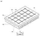
- FIG. 2 is an exploded perspective view of the circuit device 100.
- the circuit device 100 further includes a first heat sink 30, a plurality of first partition plates 41, and a plurality of second partition plates .
- the first heat sink 30 has an upper surface 30a and a lower surface 30b.
- the lower surface 30b is the opposite surface of the upper surface 30a.
- first direction DR1 the direction along the normal line of upper surface 30a
- second direction DR2 a direction orthogonal to the first direction DR1 and the second direction DR2 is defined as a third direction DR3.
- a plurality of fins 30c are formed on the lower surface 30b.
- the fin 30c extends, for example, in the second direction DR2.
- the plurality of fins 30c are spaced apart from each other in the third direction DR3.
- the first heat sink 30 is made of a metal material having excellent thermal conductivity, such as copper (copper alloy) or aluminum (aluminum alloy).
- the first heat sink 30 is formed, for example, by extrusion. Extrusion is performed, for example, along the extending direction (second direction DR2) of the fins 30c.
- the first partition plate 41 is attached to the upper surface 30a.
- the first partition plate 41 extends in the second direction DR2.
- the plurality of first partition plates 41 are spaced apart from each other in the third direction DR3.
- a rolled material made of a metal material having excellent thermal conductivity such as copper (copper alloy) or aluminum (aluminum alloy) is used.
- the second partition plate 42 is attached to the upper surface 30a.
- the second partition plate 42 extends in the third direction DR3.
- the plurality of second partition plates 42 are spaced apart from each other in the second direction DR2.
- the first partition plate 41 and the second partition plate 42 are attached to the upper surface 30a in a grid pattern.
- a rolled material made of a metal material having excellent thermal conductivity such as copper (copper alloy) or aluminum (aluminum alloy) is used.
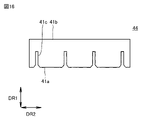
- FIG. 3 is a plan view of the first partition plate 41 included in the circuit device 100.
- the first partition plate 41 has a first end 41a and a second end 41b.
- the first end 41a is the end on the upper surface 30a side.
- the second end 41b is the end opposite to the first end 41a.
- the first partition plate 41 is formed with a plurality of first insertion openings 41c.
- the first insertion port 41c extends from the first end 41a toward the second end 41b.
- the plurality of first insertion ports 41c are spaced apart from each other in the second direction DR2.
- the first insertion port 41c penetrates the first partition plate 41 along the thickness direction.
- FIG. 4 is a plan view of the second partition plate 42 included in the circuit device 100.
- the second partition plate 42 has a third end 42a and a fourth end 42b.
- the third end 42a is the end on the upper surface 30a side.
- the fourth end 42b is the end opposite to the third end 42a.
- the second partition plate 42 is formed with a plurality of second insertion openings 42c.
- the second insertion port 42c extends from the fourth end 42b toward the third end 42a.
- the plurality of second insertion ports 42c are spaced apart from each other in the third direction DR3.
- the second insertion port 42c penetrates the second partition plate 42 along the thickness direction.
- the first insertion port 41c is inserted into the second insertion port 42c. This prevents the first partition plate 41 and the second partition plate 42 from interfering with each other.
- the first partition plate 41 and the second partition plate 42 intersect each other as described above. For example, they may be fixed by fitting, caulking, welding, or the like so as to fill the gaps around the respective insertion openings. For example, if each of the above gaps is small enough to prevent liquid from leaking, it may not be completely fixed.
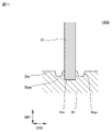
- FIG. 5 is a cross-sectional view of the circuit device 100.
- the circuit device 100 further has a sealing material 50.
- the sealing material 50 fills a space defined by two first partition plates 41 adjacent in the third direction DR3, two second partition plates 42 adjacent in the second direction DR2, and the upper surface 30a. .
- the first circuit component 10 (capacitor 10a) is arranged inside the sealing material 50 .
- the capacitor 10a has an exterior case 10aa, a sealing resin 10ab, a capacitor element body 10ac, and lead wires 10ad.
- the exterior case 10aa is filled with a sealing resin 10ab.
- a capacitor element body 10ac is arranged in the sealing resin 10ab.
- the capacitor element main body 10ac is formed by winding a dielectric film on which a metal foil is layered.
- the lead wire 10ad is electrically connected to the capacitor element body 10ac. A part of the lead wire 10ad is located outside the exterior case 10aa.
- the sealing material 50 has, for example, a heat dissipation auxiliary material 51 and a mold material 52 .
- the auxiliary heat dissipation material 51 is applied on the upper surface 30a.
- the auxiliary heat dissipation material 51 is in contact with the first circuit component 10 (capacitor 10a). More specifically, the auxiliary heat dissipation member 51 is in contact with the top surface of the exterior case 10aa.
- the molding material 52 is arranged on the heat radiation auxiliary material 51 .
- the molding material 52 is in contact with the first circuit component 10 (side surface of the exterior case 10aa), the first partition plate 41 and the second partition plate 42. As shown in FIG.
- the auxiliary heat dissipation material 51 is composed of an adhesive, grease, gel, or insulating sheet made of a resin material such as silicone resin, epoxy resin, or urethane resin.
- the auxiliary heat dissipation material 51 may be mixed with thermally conductive fillers such as ceramics or metals in order to improve thermal conductivity.
- the auxiliary heat dissipation material 51 may be a material having a thermal conductivity of, for example, 1 W/m ⁇ K to several tens of W/m ⁇ K.
- the molding material 52 is made of a resin material with high thermal conductivity.
- the molding material 52 is made of, for example, epoxy resin, silicone resin, urethane resin, PPS (polyphenylene sulfide) resin, PEEK (polyetheretherketone) resin, or ABS (acrylonitrile-butadiene-styrene) resin containing thermally conductive filler. may be configured.
- the Young's modulus of the molding material 52 may be 1 MPa or more and 50 GPa or less.
- the thermal conductivity of the molding material 52 may be 0.1 W/m ⁇ K or more and 20 W/m ⁇ K or less. Vibration resistance and environmental resistance are improved by sealing the molding material 52 .
- the auxiliary heat dissipation material 51 and the molding material 52 may be made of the same material.
- the auxiliary heat dissipation material 51 and the molding material 52 may be an adhesive.
- the circuit device 100 further has a printed wiring board 60 .
- the printed wiring board 60 is arranged on the first partition plate 41 and the second partition plate 42 .
- the printed wiring board 60 is electrically connected to the plurality of first circuit components 10 . More specifically, the terminals of the first circuit component 10 (the lead wires 10ad when the first circuit component 10 is the capacitor 10a) are inserted into the printed wiring board 60. As shown in FIG. Thus, the wiring of the peripheral circuit 110 shown in FIG. 1 is realized.
- the first partition plate 41 and the second partition plate 42 are attached to the upper surface 30a. More specifically, the first partition plate 41 is fitted into the second partition plate 42 with the second partition plate 42 arranged on the upper surface 30a. Secondly, a heat dissipation auxiliary material 51 is applied on the upper surface 30a. Third, the first circuit component 10 is arranged in a space defined by two adjacent first partition plates 41, two adjacent second partition plates 42, and the upper surface 30a. Fourth, a mold material 52 is injected into the space. Fifth, after the molding material 52 is cured, the first circuit component 10 and the printed wiring board 60 are connected. This connection is made, for example, by soldering.
- the top surface of the first circuit component 10 is in contact with the first heat sink 30 via the encapsulant 50 (heat dissipation auxiliary member 51). Further, in the circuit device 100, the side surfaces of the first circuit component 10 are in contact with the first partition plate 41 and the second partition plate 42 via the sealing material 50 (mold material 52). Therefore, the first circuit component 10 radiates heat from the side surfaces and the top surface, thereby improving the heat radiation performance.
- the life of the first circuit component 10 is improved.
- the first circuit component 10 is the capacitor 10a
- a temperature reduction of 10° C. approximately doubles the life.
- the first circuit component 10 is the inductor 10b
- the temperature reduction of 10° C. approximately doubles the life of the enamel coating of the inductor 10b.
- the first circuit component 10 is the discharge resistor 10d and the charge resistor 10e
- the temperature is reduced, so that the rank of the power category of the discharge resistor 10d and the charge resistor 10e can be lowered due to temperature derating.
- the number of series or parallel connections of the discharge resistor 10d and the charge resistor 10e can be reduced.
- heat diffusion heat radiation
- first partition plate 41 second partition plate 42
- an electrically optimal arrangement of the first circuit component 10 can be achieved without being subject to thermal restrictions.
- a plurality of first partition plates 41 and second partition plates 42 having high thermal conductivity are arranged. Therefore, the temperature of the first circuit component 10, which has different temperatures during normal operation, is equalized.
- the first circuit component 10 placed near the center of the circuit device 100 receives heat from the first circuit components 10 placed around it. temperature increases.
- the first circuit component 10 arranged in the outer peripheral portion of the circuit device 100 has a small temperature rise because there are few first circuit components 10 around it.
- the amount of temperature rise of the first circuit component 10 differs depending on the arrangement position, and a temperature difference occurs between the first circuit components 10 arranged at different positions.
- the plurality of the first partition plates 41 and the second partition plates 42 having high thermal conductivity are arranged, so that the temperature of the first circuit components 10 arranged in plurality can be equalized. can reduce the difference. Since the temperature derating is determined by the first circuit component 10 having the largest temperature rise, the circuit device 100 can be used more effectively when the temperature difference among the plurality of first circuit components 10 is smaller.
- the first partition plate 41 and the second partition plate 42 function as electromagnetic shields.
- the first circuit component 10 is the inductor 10b
- the leakage magnetic flux from the inductor 10b is shielded by the first partition plate 41 and the second partition plate 42, so that the sensor components (current sensor, etc.) can be improved.
- the first partition plate 41 and the second partition plate 42 function as firewalls.
- one of the first circuit components 10 is the capacitor 10a
- the sparks are blocked by the first partition plate 41 and the second partition plate 42, and other A shock to the 1-circuit component 10 is prevented.
- a space defined by two adjacent first partition plates 41, two adjacent second partition plates 42, and the upper surface 30a is filled with a sealing material 50 (mold material 52). Therefore, the vibration resistance characteristics of the first circuit component 10 can be improved.
- the circuit device 100 is a structure configured by combining the first partition plate 41 , the second partition plate 42 and the first heat sink 30 . Therefore, it is possible to increase or decrease the number of squares formed by the first partition plate 41 and the second partition plate 42 according to the number or size of the first circuit component 10 . Moreover, in the circuit device 100, the thickness, type, thickness, etc. of the first partition plate 41 and the second partition plate 42 can be arbitrarily selected. In addition, in the circuit device 100, the first partition plate 41 and the second partition plate 42 are subjected to bending and uneven press working to ensure the strength of the first partition plate 41 and the second partition plate 42 and to form a grid shape. mass shape changes are possible. As a result, the circuit device 100 can flexibly implement various specifications at low cost.
- the first circuit component 10 is arranged in the space defined by the two adjacent first partition plates 41, the two adjacent second partition plates 42, and the upper surface 30a.
- the insertion of the first circuit component 10 is easy, and the terminal position of the first circuit component 10 can be positioned at the same time as the insertion.
- the connection of the first circuit component 10 is performed by inserting the terminals of the first circuit component 10 into the printed wiring board 60, the assembly of the printed wiring board 60 is also easy.
- the connection between the first circuit components 10 is performed using the printed wiring board 60, the electrical connection between the first circuit components 10 can be freely performed.
- connection (soldering) between the terminals of the first circuit component 10 and the printed wiring board 60 can be performed using a flow solder bath or a point soldering device. That is, since the terminals of the first circuit component 10 and the printed wiring board 60 can be connected using the existing equipment, the equipment investment can be suppressed.
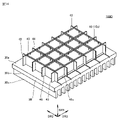
- FIG. 6 is a perspective view of a circuit device 100 according to a modification.
- circuit device 100 may further include case 70 .
- the case 70 is arranged on the upper surface 30 a so as to be positioned outside the first partition plate 41 and the second partition plate 42 .
- the first partition plate 41 and the second partition plate 42 are not fixed to the first heat sink 30 even if the first partition plate 41 and the second partition plate 42 are not fixed to the first heat sink 30.
- the space defined by the second partition plate 42 and the first heat sink 30 can be filled with the sealing material 50 .
- any of the capacitor 10a, the inductor 10b, the contactor 10c, the discharge resistor 10d, and the charge resistor 10e may be arranged as the first circuit component 10 used in the circuit device 100. Any component that generates heat can be used as the first circuit component 10 of the circuit device 100 without being limited to these.
- only one first circuit component 10 may be arranged in one section, or a plurality of first circuit components 10 may be arranged in one section.
- the one first circuit component 10 can use all the cooling capacity of the one section.
- the cooling capacity is divided, if the first circuit components 10 are small and the section is large, the first circuit components 10 can be arranged more efficiently. .
- the circuit device 100 may have a section (arrangement section) in which the first circuit component 10 is arranged and a section (non-arrangement section) in which the first circuit component 10 is not arranged.
- the cooling effect of the first circuit component 10 arranged in the arrangement section adjacent to the non-arrangement section can be further enhanced, and the first circuit component 10 can be cooled more effectively.
- circuit device 100A A circuit device (hereinafter referred to as "circuit device 100A") according to the second embodiment will be described. Here, differences from the circuit device 100 will be mainly described, and redundant description will not be repeated.
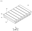
- FIG. 7 is a perspective view of the first heat sink 30 included in the circuit device 100A.
- a plurality of first grooves 30d and a plurality of second grooves 30e are formed in the upper surface 30a.
- the first groove 30d extends in the second direction DR2.
- the multiple first grooves 30d are spaced apart from each other in the third direction DR3.
- the second groove 30e extends in the third direction DR3.
- the multiple second grooves 30e are spaced apart from each other in the second direction DR2.
- FIG. 8 is a cross-sectional view of the circuit device 100A in the vicinity of the first groove 30d.
- FIG. 9 is a cross-sectional view of the circuit device 100A in the vicinity of the second groove 30e.
- the first partition plate 41 and the second partition plate 42 are inserted into the first groove 30d and the second groove 30e, respectively. More specifically, the first end 41a side of the first partition plate 41 and the third end 42a side of the second partition plate 42 are inserted into the first groove 30d and the second groove 30e, respectively.
- the first partition plate 41 and the second partition plate 42 are brazed to the first groove 30d and the second groove 30e with the brazing material 31, respectively. That is, the first partition plate 41 and the second partition plate 42 are metal-bonded to the first groove 30d and the second groove 30e, respectively.
- the first partition plate 41 and the second partition plate 42 may be welded (metallic joint) to the first groove 30d and the second groove 30e, respectively.
- the first partition plate 41 does not have to be brazed (welded) at all the portions inserted into the first grooves 30d.
- the second partition plate 42 does not need to be brazed (welded) at all portions disposed within the second grooves 30e.
- the first partition plate 41 and second partition plate 42 and the first heat sink 30 are metal-bonded. Since the contact thermal resistance is reduced, the heat dissipation performance of the first circuit component 10 is further improved.
- the first partition plate 41 and the second partition plate 42 are inserted into the first groove 30d and the second groove 30e, respectively.
- the positioning accuracy of the first partition plate 41 and the second partition plate 42 is improved. By improving the positioning accuracy, the distance between the first partition plate 41 and the second partition plate 42 and the first circuit component 10 (capacitor 10a) can be set with high accuracy. Thereby, the thickness of the sealing material 50 can be reduced, and the thermal resistance can be reduced. Furthermore, by fixing the first partition plate 41 and the second partition plate 42 to the first heat sink 30 , the space defined by the first partition plate 41 , the second partition plate 42 and the first heat sink 30 can be more reliably An encapsulant 50 can be filled.
- the first groove 30d may be formed to reach both ends of the upper surface 30a in the second direction DR2. In this case, when forming the first heat sink 30 by extrusion, the first groove 30d can be formed at the same time.
- the first groove 30d (second groove 30e) may be widened at the portion where it crosses the second groove 30e (first groove 30d). Further, the first groove 30d (second groove 30e) may be widened at the end in the second direction DR2 (third direction DR3). In these cases, it is possible to prevent the brazing filler metal 31 from overflowing from the first groove 30d (the second groove 30e) and resulting in manufacturing defects in the widened portion.
- circuit device 100B A circuit device (hereinafter referred to as "circuit device 100B") according to the third embodiment will be described. Here, differences from the circuit device 100A will be mainly described, and redundant description will not be repeated.
- FIG. 10 is a cross-sectional view of the circuit device 100B in the vicinity of the first groove 30d.
- FIG. 11 is a cross-sectional view of the circuit device 100B in the vicinity of the second groove 30e.
- the upper surface 30a is formed with caulked grooves 30fa and 30fb, and caulked grooves 30ga and 30gb.
- the crimped grooves 30fa and the crimped grooves 30fb extend in the second direction DR2.
- the caulking grooves 30fa and the caulking grooves 30fb are arranged so as to sandwich the first groove 30d in the third direction DR3.
- the crimped groove 30ga and the crimped groove 30gb extend in the third direction DR3.
- the caulking grooves 30fa and the caulking grooves 30fb are arranged so as to sandwich the second grooves 30e in the third direction DR3.
- the first partition plate 41 is crimped into the first groove 30d. More specifically, the portion of the first heat sink 30 between the first groove 30d and the crimped groove 30fa and the portion of the first heat sink 30 between the first groove 30d and the crimped groove 30fb are the first partition plates. The first partition plate 41 is crimped into the first groove 30d by plastic deformation toward the 41 side.
- the second partition plate 42 is crimped into the second groove 30e. More specifically, the portion of the first heat sink 30 between the second groove 30e and the crimped groove 30ga and the portion of the first heat sink 30 between the second groove 30e and the crimped groove 30gb are the second partition plates. The second partition plate 42 is crimped into the second groove 30e by being plastically deformed toward the 42 side.
- first partition plate 41 it is not necessary for the first partition plate 41 to be caulked at all portions inserted into the first grooves 30d. Further, the second partition plate 42 does not need to be caulked at all portions disposed within the second grooves 30e. For example, the crimping of the first partition plate 41 and the second partition plate 42 may not be performed at the portion where the first groove 30d and the second groove 30e intersect.
- first partition plate 41 second partition plate 42
- second partition plate 42 the other portion of the first partition plate 41 (second partition plate 42) is crimped. may This temporary fixation may be performed by spot welding.
- the first partition plate 41 and the second partition plate 42 and the first heat sink 30 are metal-bonded by caulking, and the first partition plate 41 and the second partition plate 42 and the first heat sink 30 Since the contact thermal resistance of the first circuit component 10 is reduced, the heat dissipation performance of the first circuit component 10 is further improved.
- the first partition plate 41 and the second partition plate 42 are inserted into the first groove 30d and the second groove 30e, respectively. In addition, the positioning accuracy of the first partition plate 41 and the second partition plate 42 is improved.
- the rest of the first partition plate 41 (second partition plate 42) is crimped.
- the position of the first partition plate 41 (second partition plate 42) can be finely adjusted after temporary fixing, the positional accuracy of the first partition plate 41 (second partition plate 42) can be further improved.
- a groove extending in the second direction DR2 may be formed in the lower surface 30b.
- the fins 30c may be configured by inserting plate members into the grooves. The crimping of the grooves of the plate member is performed by the same method as the crimping of the first partition plate 41 and the second partition plate 42, for example.
- circuit device 100C A circuit device (hereinafter referred to as "circuit device 100C") according to the fourth embodiment will be described. Here, differences from the circuit device 100 will be mainly described, and redundant description will not be repeated.
- FIG. 12 is a cross-sectional view of the circuit device 100C.
- FIG. 12 shows a cross section of the circuit device 100C at a position corresponding to FIG.
- the capacitor 10a does not have the exterior case 10aa and the sealing resin 10ab.
- the circuit device 100C further has an insulating net 11 .
- the insulating net 11 is made of an insulating resin material.
- the insulating net 11 is arranged in a space defined by two adjacent first partition plates 41, two adjacent second partition plates 42, and the upper surface 30a so as to cover the capacitor body 10ac. That is, the insulating net 11 is positioned between the capacitor element body 10ac and the upper surface 30a, between the capacitor element body 10ac and the first partition plate 41, and between the capacitor element body 10ac and the second partition plate 42. .
- the sealing material 50 does not have to be composed of the auxiliary heat dissipation material 51 and the molding material 52.
- the sealing material 50 is formed by potting an arbitrary resin material.
- This resin material is, for example, silicone.
- the insulating net 11 may be made of, for example, epoxy resin, silicone resin, urethane resin, PPS resin, PEEK resin, or ABS resin.
- the insulating net 11 may be made of a flexible and stretchable rubber material. Although the capacitor 10a and the insulating net 11 are not in contact in FIG. 12, the capacitor 10a and the insulating net 11 may be in contact. It is sufficient that the capacitor 10a is prevented from coming into contact with the first partition plate 41, the second partition plate 42 and the upper surface 30a by the insulating net 11.
- the capacitor 10a does not have the exterior case 10aa. Therefore, the cross-sectional area of the capacitor element body 10ac (the number of turns of the metal foil and the dielectric film in the capacitor element body 10ac) can be increased. Thus, according to the circuit device 100C, the capacitance per capacitor 10a can be increased.
- the insulating net 11 and the sealing material 50 are arranged between the capacitor 10a (capacitor element main body 10ac) and the upper surface 30a, the first partition plate 41 and the second partition plate 42, the exterior case 10aa and Even without the sealing resin 10ab, the insulation between the capacitor 10a (capacitor element body 10ac) and the upper surface 30a, the first partition plate 41 and the second partition plate 42 can be ensured.
- the capacitor 10a that does not have the exterior case 10aa can be used, so the cost of the capacitor 10a can be reduced.
- the capacitor 10a (capacitor element main body 10ac) can be sealed only with a resin having a low thermal resistance such as silicone as the sealing material 50. Therefore, the heat generated by the capacitor 10a is efficiently transferred to the first heat sink 30. can do.
- the insulating net 11 was used as a member for ensuring insulation between the capacitor 10a (capacitor element main body 10ac) and the upper surface 30a, the first partition plate 41 and the second partition plate 42.
- an insulating paper or a heat-conducting insulating sheet may be used.
- a spacer may be used instead of the insulating net 11. By disposing this spacer between capacitor element main body 10ac, first partition plate 41, second partition plate 42 and upper surface 30a, capacitor element main body 10ac, first partition plate 41, second partition plate 42 and upper surface 30a are separated from each other. Contact with 30a is prevented.
- circuit device 100D A circuit device (hereinafter referred to as “circuit device 100D”) according to Embodiment 5 will be described. Here, differences from the circuit device 100 will be mainly described, and redundant description will not be repeated.
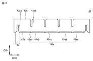
- FIG. 13 is a perspective view of the first heat sink 30 included in the circuit device 100D. As shown in FIG. 13, grooves 30h are formed in the upper surface 30a. The groove 30h extends in the second direction DR2. Groove 30h is preferably formed to reach both ends of upper surface 30a in second direction DR2.
- FIG. 14 is a perspective view of the circuit device 100D.
- illustration of the sealing material 50 and the printed wiring board 60 is omitted.
- first partition plates 43 those arranged at both ends in the third direction DR3
- first partition plates 43 those arranged at other than both ends in the third direction DR3
- a partition plate 44 is used.
- second partition plates 45 those arranged at both ends in the second direction DR2 are referred to as second partition plates 45
- Two partition plates 46 are provided.
- FIG. 15 is a plan view of the first partition plate 43 included in the circuit device 100D. As shown in FIG. 15, in the first partition plate 43, the first insertion port 41c extends from the second end 41b toward the first end 41a.
- FIG. 16 is a plan view of the first partition plate 44 included in the circuit device 100D. As shown in FIG. 16, in the first partition plate 44, the first insertion port 41c extends from the first end 41a toward the second end 41b.
- FIG. 17 is a plan view of the second partition plate 45 included in the circuit device 100D. As shown in FIG. 17, in the second partition plate 45, the second insertion port 42ca extends from the third end 42a toward the fourth end 42b, and the second insertion port 42cb extends toward the fourth end 42b. , toward the third end 42a.
- the second partition plate 45 has a support portion 45a.
- the support portion 45a extends in the second direction DR2 on the side opposite to the second partition plate 46 .
- the support portion 45a is formed by bending the third end 42a side of the second partition plate 45 .
- the support portion 45a may be divided into a plurality of portions in the third direction DR3 (in the example of FIG. 17, a first portion 45aa, a second portion 45ab, a third portion 45ac, a fourth portion 45ad and a divided into a fifth portion 45ae).
- FIG. 18 is a plan view of the second partition plate 46 included in the circuit device 100D. As shown in FIG. 18, in the second partition plate 46, the second insertion port 42ca extends from the third end 42a toward the fourth end 42b, and the second insertion port 42cb extends toward the fourth end 42b. , toward the third end 42a.
- the width W at the third end 42a of the second insertion port 42ca of the second partition plate 45 is preferably larger than the width at the fourth end 42b of the second insertion port 42cb of the second partition plate 45. Also, the width W is larger than the width at the second end 41b of the first insertion port 41c of the first partition plate 43 and the width at the first end 41a of the first insertion port 41c of the first partition plate 44. is preferred. Furthermore, the width W is larger than the width at the third end 42a of the second insertion port 42ca of the second partition plate 46 and the width at the fourth end 42b of the second insertion port 42cb of the second partition plate 46. is preferred.
- the first partition plate 43, the first partition plate 44, the second partition plate 45, and the second partition plate 46 are attached to the upper surface 30a by the following method.
- the first partition plates 43 are inserted into the grooves 30h located at both ends in the third direction DR3.
- the second partition plate 45 is assembled to the first partition plate 43 by inserting the second insertion openings 42ca into the first insertion openings 41c of the first partition plate 43 located at both ends in the second direction DR2.
- the first partition plate 43 and the second partition plate 45 are generally upright.
- the second partition plate 46 is assembled to the first partition plate 43 by inserting the second insertion openings 42ca into the first insertion openings 41c of the first partition plate 43 located at positions other than both ends in the second direction DR2. .
- the width of the first insertion port 41c and the width of the second insertion port 42ca of the second partition plate 46 are smaller than the width W. can also be easily inserted. Since the first partition plate 43 and the second partition plate 45 are already substantially upright, the second partition plate 46 is also substantially upright.
- the first partition plate 44 is connected to the second partition plate 45 and the second partition plate 46.
- the width of the first insertion port 41c and the width of the second insertion port 42cb are smaller than the width W. can also be easily inserted.
- the first partition plate 44 is inserted into the grooves 30h positioned other than both ends in the third direction DR3.
- first partition plate 43, the first partition plate 44, the second partition plate 45 and the second partition plate 46 are fixed to the upper surface 30a.
- the fixing of the first partition plate 43 and the first partition plate 44 to the upper surface 30a is performed, for example, by caulking the grooves 30h.
- the fixing of the second partition plate 45 and the second partition plate 46 to the upper surface 30a is performed by fillet welding, for example.
- the step of forming the grooves can be simplified. Since the groove 30h extends in the second direction DR2 (the same direction as the fins 30c), it can be formed at the same time as the first heat sink 30 is formed by extrusion.
- the assembly of the first partition plate 43, the first partition plate 44, the second partition plate 45, and the second partition plate 46 can be performed with minimum holding, so that the assembly process can be automated. It is possible to reduce man-hours and simplify jigs.
- the second partition plate 45 may be used instead of the second partition plate 46 . In this case, it is possible to reduce the manufacturing cost by sharing the members.
- Modification 2 In the circuit device 100D, some of the plurality of portions included in the support portion 45a may be bent in opposite directions.
- the first portion 45aa, the second portion 45ac, and the fifth portion 45ae extend in the third direction DR3 on the side opposite to the second partition plate 46, while the second portion 45ab and the fourth portion 45ad It may extend in the third direction DR3 toward the second partition plate 46 side. In this case, the uprightness of the second partition plate 45 can be further enhanced.
- the second partition plate 45 may be fixed to the first heat sink 30 by screwing instead of welding. More specifically, a screw hole is formed in the upper surface 30a, a through hole is formed in the support portion 45a so as to overlap the screw hole, and a screw inserted into the through hole is screwed into the screw hole. , the second partition plate 45 may be fixed to the first heat sink 30 . In this case, since the second partition plate 45 can be firmly attached to the upper surface 30a, the thermal contact resistance between the second partition plate 45 and the upper surface 30a can be reduced. When the screwing is performed in the area where the first circuit component 10 is arranged, it is preferable to prevent the head of the screw from protruding by performing countersunk screw processing on the support portion 45a. .
- circuit device 100E A circuit device (hereinafter referred to as "circuit device 100E") according to Embodiment 6 will be described. Here, differences from the circuit device 100 will be mainly described, and redundant description will not be repeated.
- FIG. 19 is a perspective view of the circuit device 100E. As shown in FIG. 19, circuit device 100E further includes second heat sink 80 and heat pipe 90 . In addition, in the circuit device 100E, the first heat sink 30 does not have the fins 30c.
- the second heat sink 80 has an upper surface 80a and a lower surface 80b.
- the second circuit component 20 is arranged on the upper surface 80a.
- the lower surface 80b is the opposite surface of the upper surface 80a.
- a plurality of fins 80c are formed on the lower surface 80b.
- the heat pipe 90 thermally connects the first heat sink 30 and the second heat sink 80 . More specifically, the heat pipe 90 is filled with a liquid (for example, pure water). Pure water in the heat pipe 90 evaporates due to heat from the first heat sink 30 . That is, the pure water in the heat pipe 90 absorbs latent heat of evaporation from the first heat sink 30 and cools the first heat sink 30 . The evaporated pure water in the heat pipe 90 moves to the second heat sink 80 side. The portion of heat pipe 90 between first heat sink 30 and second heat sink 80 is insulated.
- a liquid for example, pure water
- the pure water in the heat pipe 90 that has moved toward the second heat sink 80 releases latent heat of evaporation to the second heat sink 80 and condenses.
- the condensed pure water in the heat pipe 90 returns to the first heat sink 30 side due to the capillary structure (wick) provided on the inner wall of the heat pipe 90 .
- the first heat sink 30 and the second heat sink 80 are thermally connected by the heat pipe 90 .
- the heat from the first heat sink 30 radiated to the second heat sink 80 is intensively radiated by the second heat sink 80 .
- the heat pipe 90 does not have to pass through the interior of the first heat sink 30 and the second heat sink 80 .
- the heat pipe 90 should be in contact with at least the first heat sink 30 and the second heat sink 80 .
- circuit device 100E fect of circuit device 100E
- the first heat sink 30 can be simplified and miniaturized, the volume and cost of the first heat sink 30 can be reduced.
- the circuit device 100E does not require an individual cooling space such as an air passage, the space efficiency of the device as a whole is improved, so that the device can be made smaller.
- the first heat sink 30 can be arranged at any location. More specifically, the first heat sink 30 can be arranged in an electrically optimal place, for example, in the vicinity of the second circuit component 20 or in a place where the wiring length can be shortened (wiring inductance can be reduced). .
- the electrical performance of the entire device or the switching circuit 120 can be improved. For example, it is possible to reduce loss associated with shortening the wiring length, and suppress switching surges associated with reducing the wiring inductance.
- circuit device 100F A circuit device (hereinafter referred to as "circuit device 100F") according to Embodiment 7 will be described. Here, differences from the circuit device 100 will be mainly described, and redundant description will not be repeated.
- FIG. 20 is a perspective view of the circuit device 100F. In FIG. 20, illustration of the printed wiring board 60 is omitted.
- FIG. 21 is a cross-sectional view of the circuit device 100F. FIG. 21 shows a cross section of the circuit device 100F at a position corresponding to FIG. As shown in FIGS. 20 and 21, in the circuit device 100F, slits 53 and slits 54 are formed in the surface of the sealing material 50 (molding material 52) on the printed wiring board 60 side.
- the slit 53 extends in the second direction DR2.
- the slit 54 extends in the third direction DR3.
- the slits 53 and 54 have, for example, a U shape in cross-sectional view perpendicular to their extending directions.
- the slits 53 and 54 may have a V shape in a cross-sectional view orthogonal to their extending directions. Either one of the slit 53 and the slit 54 may not be formed.
- the width of the slit 53 and the width of the slit 54 are preferably 1 mm or more.
- the formation of the slits 53 and the formation of the slits 54 may be performed after the sealing material 50 (mold material 52) is cured, or may be performed before the sealing material 50 (mold material 52) is cured.
- Capacitor 10a may expand when it fails. In the circuit device 100F, stress tends to concentrate on the portion where the slit 53 is formed and the portion where the slit 54 is formed, and the strength is relatively low in these portions. Therefore, in the circuit device 100F, even if the capacitor 10a expands due to a failure, the sealing material 50 (mold material 52) is broken near the slits 53 and 54 to alleviate the force associated with the expansion. Explosion of the sealing material 50 (mold material 52) can be suppressed.
- the slits 53 and 54 are formed, so that the insulation distance between the two terminals of the capacitor 10a can be increased.
- the slits 53 and 54 are formed before the sealing material 50 (mold material 52) is cured, thereby suppressing the occurrence of short circuits due to dust and conductive foreign matter generated during the slit forming process.
- circuit device 100G A circuit device (hereinafter referred to as “circuit device 100G”) according to Embodiment 8 will be described. Here, differences from the circuit device 100 will be mainly described, and redundant description will not be repeated.
- FIG. 22 is a cross-sectional view of the circuit device 100G.
- FIG. 22 shows a cross section of the circuit device 100G at a position corresponding to FIG.
- silicone gel 55 is used in place of molding material 52 in circuit device 100G.
- the silicone gel 55 is made of a material with low viscosity.
- the silicone gel 55 may be used instead of the sealing material 50 (see FIG. 12) in the circuit device 100C.
- the silicone gel 55 has high insulating performance.
- the silicone gel 55 since the silicone gel 55 has high adhesion to the capacitor 10a, the first partition plate 41 and the second partition plate 42, there is no need to consider the creepage at the boundary with these parts/members. This eliminates the need for an insulating area for securing the creepage surface, making it possible to reduce the size of the periphery of the capacitor 10a.
- the use of the silicone gel 55 can ensure high insulation (high creeping dielectric strength and penetration dielectric strength).
- the heat radiation performance from the capacitor 10a can be improved at the same time.
- the silicone gel 55 is a highly penetrating (soft) material, the reliability of the circuit device 100G is improved when heat cycles or power cycles are applied. Since the capacitor 10a is also fixed in position by the printed wiring board 60, even if the silicone gel 55 is used, the positional fixation of the capacitor 10a is not hindered.
- Second circuit component 10 First circuit component 10a Capacitor 10aa Exterior case 10ab Sealing resin 10ad Lead wire 10b Inductor 10c Contactor 10d Discharging resistor 10e Charging resistor 11 Insulating net 20 Second circuit component 20a, 20b, 20c, 20d, 20e, 20f transistors, 20g, 20h, 20i, 20j, 20k, 20l diodes, 30 first heat sink, 30a upper surface, 30b lower surface, 30c fins, 30d first groove, 30e second groove, 30fa, 30fb, 30ga, 30gb crimped groove, 30h groove, 31 brazing material, 41 first partition plate, 41a first end, 41b second end, 41c first insertion port, 42 second partition plate, 42a third end, 42b fourth end , 42c, 42ca, 42cb second insertion port, 43, 44 first partition plate, 45 second partition plate, 45a support portion, 45aa first portion, 45ab second portion, 45ad fourth portion, 45ae fifth portion, 46 Second
Abstract
回路装置(100)は、第1上面(30a)を有する第1ヒートシンク(30)と、第1上面に取り付けられている複数の第1仕切り板(41)及び第2仕切り板(42)と、封止材(50)と、第1回路部品(10)と、プリント配線板(60)とを備える。第1上面の法線方向は、第1方向(DR1)に沿っている。第1仕切り板は、第1方向に直交している第2方向(DR2)に延在している。第2仕切り板は、第1方向及び第2方向に直交している第3(DR3)方向に延在している。封止材は、隣り合う2つの第1仕切り板、隣り合う2つの第2仕切り板及び第1上面により画されている空間に、充填されている。第1回路部品は、封止材内に配置されている。プリント配線板は、第1仕切り板及び第2仕切り板上に配置されており、かつ第1回路部品に電気的に接続されている。
Description
本開示は、回路装置に関する。
特開2016-66666号公報(特許文献1)には、コンデンサが記載されている。特許文献1に記載のコンデンサは、蓋体と、電極板と、コンデンサ素子と、ケースとを有している。蓋体は、基板と、フィンとを有している。フィンは、基板の一方の面上に配置されている。電極板は、基板の他方の面上に配置されている。コンデンサ素子は、電極板上に配置されている。ケースは、電極板及びコンデンサ素子を覆うように蓋体上に配置されている。
特許文献1に記載のコンデンサでは、コンデンサ素子からの発熱が、コンデンサ素子の下面(電極板に接触している面)において電極板及び蓋体に伝熱される。しかしながら、コンデンサ素子の他の面は、放熱に寄与してない。すなわち、特許文献1に記載のコンデンサは、放熱性能に改善の余地がある。
本開示は、上記のような従来技術の問題点に鑑みてなされたものである。より具体的には、本開示は、回路部品の放熱性能が改善された回路装置を提供する。
本開示の回路装置は、第1上面を有する第1ヒートシンクと、第1上面に取り付けられている複数の第1仕切り板及び第2仕切り板と、封止材と、第1回路部品と、プリント配線板とを備える。第1上面の法線方向は、第1方向に沿っている。第1仕切り板は、第1方向に直交している第2方向に延在している。第2仕切り板は、第1方向及び第2方向に直交している第3方向に延在している。封止材は、隣り合う2つの第1仕切り板、隣り合う2つの第2仕切り板及び第1上面により画されている空間に充填されている。第1回路部品は、封止材内に配置されており、熱的及び機械的に結合されている。プリント配線板は、第1仕切り板及び第2仕切り板上に配置されており、かつ第1回路部品に電気的に接続されている。
本開示の回路装置によると、回路部品の放熱性能を改善することができる。
本開示の実施形態の詳細を、図面を参照しながら説明する。以下の図面においては、同一又は相当する部分に同一の参照符号を付し、重複する説明は繰り返さない。
実施の形態1.
実施の形態1に係る回路装置(以下「回路装置100」とする)を説明する。
実施の形態1に係る回路装置(以下「回路装置100」とする)を説明する。
(回路装置100の構成)
回路装置100は、例えば、電力変換装置である。回路装置100は、電力変換装置に限られるものではないが、以下においては、電力変換装置を回路装置100の例として説明する。図1は、回路装置100の回路図である。図1に示されるように、回路装置100は、周辺回路110と、スイッチング回路120とを有している。
回路装置100は、例えば、電力変換装置である。回路装置100は、電力変換装置に限られるものではないが、以下においては、電力変換装置を回路装置100の例として説明する。図1は、回路装置100の回路図である。図1に示されるように、回路装置100は、周辺回路110と、スイッチング回路120とを有している。
周辺回路110は、複数の第1回路部品10を有している。図1に示される例では、複数の第1回路部品10が、コンデンサ10a、インダクタ10b、コンタクタ10c、放電抵抗10d及び充電抵抗10eである。コンデンサ10a、インダクタ10b及びコンタクタ10cは、直列に接続されている。インダクタ10bは、コンデンサ10aとコンタクタ10cとの間に配置されている。放電抵抗10d及び充電抵抗10eは、それぞれコンデンサ10a及びコンタクタ10cに並列に接続されている。周辺回路110は、直流供給回路130に接続されている。
スイッチング回路120は、例えば、3相インバータ回路である。スイッチング回路120は、複数の第2回路部品20を有している。図1に示される例では、複数の第2回路部品20が、トランジスタ20a~トランジスタ20f及びダイオード20g~ダイオード20lである。
トランジスタ20aのドレインは、コンデンサ10aの一方の電極に電気的に接続されている。トランジスタ20aのソースは、トランジスタ20bのドレインに電気的に接続されている。トランジスタ20bのソースは、コンデンサ10aの他方の電極に電気的に接続されている。
ダイオード20gのアノードは、トランジスタ20aのソースに電気的に接続されている。ダイオード20gのカソードは、トランジスタ20aのドレインに電気的に接続されている。ダイオード20hのアノードは、トランジスタ20bのソースに電気的に接続されている。ダイオード20hのカソードは、トランジスタ20bのドレインに電気的に接続されている。
なお、トランジスタ20c、トランジスタ20d、ダイオード20i及びダイオード20jは、それぞれ、トランジスタ20a、トランジスタ20b、ダイオード20g及びダイオード20hと同様に接続されている。また、トランジスタ20e、トランジスタ20f、ダイオード20k及びダイオード20lは、それぞれ、トランジスタ20a、トランジスタ20b、ダイオード20g及びダイオード20hと同様に接続されている。図示されていないが、トランジスタ20a~トランジスタ20fのゲートは、制御回路に接続されている。
スイッチング回路120は、モータ140に接続されている。モータ140は、例えば3相モータである。モータ140は、入力線141と、入力線142と、入力線143とを有している。入力線141は、トランジスタ20aのソース及びトランジスタ20bのドレインに電気的に接続されている。入力線142は、トランジスタ20cのソース及びトランジスタ20dのドレインに電気的に接続されている。入力線143は、トランジスタ20eのソース及びトランジスタ20fのドレインに電気的に接続されている。
図2は、回路装置100の分解斜視図である。図2に示されるように、回路装置100は、第1ヒートシンク30と、複数の第1仕切り板41と、複数の第2仕切り板42とをさらに有している。
第1ヒートシンク30は、上面30aと、下面30bとを有している。下面30bは、上面30aの反対面である。以下においては、上面30aの法線に沿う方向を、第1方向DR1とする。また、以下においては、第1方向DR1に直交している方向を第2方向DR2とし、第1方向DR1及び第2方向DR2に直交している方向を第3方向DR3とする。
下面30bには、複数のフィン30cが形成されている。フィン30cは、例えば、第2方向DR2に延在している。複数のフィン30cは、第3方向DR3において互いに間隔を空けて配置されている。第1ヒートシンク30は、例えば、銅(銅合金)又はアルミニウム(アルミニウム合金)等の熱伝導性に優れる金属材料により形成されている。第1ヒートシンク30は、例えば、押出加工により形成されている。押出加工は、例えば、フィン30cの延在方向(第2方向DR2)に沿って行われる。
第1仕切り板41は、上面30aに取り付けられている。第1仕切り板41は、第2方向DR2に延在している。複数の第1仕切り板41は、第3方向DR3において、互いに間隔を空けて配置されている。第1仕切り板41には、例えば、銅(銅合金)又はアルミニウム(アルミニウム合金)等の熱伝導性に優れる金属材料により形成された圧延材が用いられる。
第2仕切り板42は、上面30aに取り付けられている。第2仕切り板42は、第3方向DR3に延在している。複数の第2仕切り板42は、第2方向DR2において、互いに間隔を空けて配置されている。このことを別の観点から言えば、第1仕切り板41及び第2仕切り板42は、上面30aに井桁状に取り付けられている。第2仕切り板42には、例えば、銅(銅合金)又はアルミニウム(アルミニウム合金)等の熱伝導性に優れる金属材料により形成された圧延材が用いられる。
図3は、回路装置100が有する第1仕切り板41の平面図である。図3に示されるように、第1仕切り板41は、第1端41aと、第2端41bとを有している。第1端41aは、上面30a側の端である。第2端41bは、第1端41aの反対側の端である。第1仕切り板41には、複数の第1差し込み口41cが形成されている。第1差し込み口41cは、第1端41aから第2端41b側に向かって延在している。複数の第1差し込み口41cは、第2方向DR2において互いに間隔を空けて配置されている。第1差し込み口41cは、厚さ方向に沿って第1仕切り板41を貫通している。
図4は、回路装置100が有する第2仕切り板42の平面図である。図4に示されるように、第2仕切り板42は、第3端42aと、第4端42bとを有している。第3端42aは、上面30a側の端である。第4端42bは、第3端42aの反対側の端である。第2仕切り板42には、複数の第2差し込み口42cが形成されている。第2差し込み口42cは、第4端42bから第3端42a側に向かって延在している。複数の第2差し込み口42cは、第3方向DR3において互いに間隔を空けて配置されている。第2差し込み口42cは、厚さ方向に沿って第2仕切り板42を貫通している。
第1差し込み口41cは、第2差し込み口42cに差し込まれている。これにより、第1仕切り板41及び第2仕切り板42が互いに干渉することが防止されている。図6においては、第1仕切り板41及び第2仕切り板42が上記のように交差しているが、外周を構成している第1仕切り板41及び第2仕切り板42同士は、組み立て後のそれぞれの差し込み口周辺にある隙間が埋まるように、例えば、嵌め合い、かしめ、溶接等により固定されてもよい。例えば上記のそれぞれの隙間が液体が漏れない程度に小さい場合、完全に固定されていなくてもよい。
図5は、回路装置100の断面図である。図5に示されるように、回路装置100は、封止材50をさらに有している。封止材50は、第3方向DR3において隣り合う2つの第1仕切り板41、第2方向DR2において隣り合う2つの第2仕切り板42及び上面30aにより画されている空間内に充填されている。
第1回路部品10(コンデンサ10a)は、封止材50内に配置されている。コンデンサ10aは、外装ケース10aaと、封止樹脂10abと、コンデンサ素子本体10acと、リード線10adとを有している。外装ケース10aa内には、封止樹脂10abが充填されている。封止樹脂10ab中には、コンデンサ素子本体10acが配置されている。コンデンサ素子本体10acは、誘電体フィルムに金属箔を重ねて巻回することにより形成されている。リード線10adは、コンデンサ素子本体10acに電気的に接続されている。リード線10adの一部は、外装ケース10aa外に位置している。
封止材50は、例えば、放熱補助材51と、モールド材52とを有している。放熱補助材51は、上面30a上に塗布されている。放熱補助材51は、第1回路部品10(コンデンサ10a)に接触している。より具体的には、放熱補助材51は、外装ケース10aaの頂面に接触している。モールド材52は、放熱補助材51上に配置されている。モールド材52は、第1回路部品10(外装ケース10aaの側面)、第1仕切り板41及び第2仕切り板42に接触している。
放熱補助材51は、シリコーン樹脂、エポキシ樹脂、ウレタン樹脂等の樹脂材料からなる接着剤、グリス、ゲル又は絶縁シートにより構成されている。放熱補助材51は、熱伝導率を向上させるために、セラミックス又は金属等の熱伝導性フィラーが混ぜられていてもよい。放熱補助材51は、例えば、熱伝導率が1W/m・K~数十W/m・Kの材料であってもよい。モールド材52は、熱伝導率が高い樹脂材料により構成されている。モールド材52は、例えば熱伝導性フィラーを含有しているエポキシ樹脂、シリコーン樹脂、ウレタン樹脂、PPS(ポリフェニレンサルファイド)樹脂、PEEK(ポリエーテルエーテルケトン)樹脂又はABS(アクリロニトリル-ブタジエン―スチレン)樹脂により構成されていてもよい。モールド材52のヤング率は、1MPa以上50GPa以下であってもよい。モールド材52の熱伝導率は、0.1W/m・K以上20W/m・K以下であってもよい。モールド材52、封止されることにより、耐振動性及び耐環境性が向上されている。放熱補助材51及びモールド材52は、同一の材料により構成されていてもよい。例えば、放熱補助材51及びモールド材52は、接着剤であってもよい。
図2に示されるように、回路装置100は、プリント配線板60をさらに有している。プリント配線板60は、第1仕切り板41及び第2仕切り板42上に配置されている。また、プリント配線板60は、複数の第1回路部品10に電気的に接続されている。より具体的には、第1回路部品10の端子(第1回路部品10がコンデンサ10aである場合、リード線10ad)が、プリント配線板60に挿入されている。これにより、図1に示されている周辺回路110の配線が実現されている。
回路装置100の組み立てにおいては、第1に、第1仕切り板41及び第2仕切り板42が上面30aに取り付けられる。より具体的には、第2仕切り板42が上面30a上に並べられた状態で、第2仕切り板42に第1仕切り板41が嵌め込まれる。第2に、上面30a上に放熱補助材51が塗布される。第3に、隣り合う2つの第1仕切り板41、隣り合う2つの第2仕切り板42及び上面30aにより画されている空間内に、第1回路部品10が配置される。第4に、上記の空間内に、モールド材52が注入される。第5に、モールド材52の硬化後、第1回路部品10とプリント配線板60との接続が行われる。この接続は、例えば、はんだ付けにより行われる。
(回路装置100の効果)
回路装置100では、第1回路部品10の頂面が封止材50(放熱補助材51)を介して第1ヒートシンク30に接触している。また、回路装置100では、第1回路部品10の側面が封止材50(モールド材52)を介して第1仕切り板41及び第2仕切り板42に接触している。そのため、第1回路部品10は、その側面及び頂面から放熱されることになり、放熱性能が改善されている。
回路装置100では、第1回路部品10の頂面が封止材50(放熱補助材51)を介して第1ヒートシンク30に接触している。また、回路装置100では、第1回路部品10の側面が封止材50(モールド材52)を介して第1仕切り板41及び第2仕切り板42に接触している。そのため、第1回路部品10は、その側面及び頂面から放熱されることになり、放熱性能が改善されている。
第1回路部品10の放熱性能が改善される結果、第1回路部品10の寿命が改善されることになる。例えば、第1回路部品10がコンデンサ10aである場合、温度が10℃低減されることにより、寿命が約2倍となる。また、第1回路部品10がインダクタ10bである場合、温度が10℃低減されることにより、インダクタ10bのエナメル被覆の寿命が約2倍となる。さらに、第1回路部品10が放電抵抗10d及び充電抵抗10eである場合、温度が低減されることにより、温度ディレーティングの関係上、放電抵抗10d及び充電抵抗10eの電力カテゴリのランクを小さくできる。その結果、放電抵抗10d及び充電抵抗10eの直列数又は並列数を減らすことができる。
回路装置100では、第1仕切り板41(第2仕切り板42)を介して隣り合う第1回路部品10の間における熱拡散(熱輻射)を抑制することができる。そのため、熱制約を受けずに、第1回路部品10の電気的に最適な配置が可能になる。例えば、コンデンサ10aと放電抵抗10dとを近接配置できる結果、コンデンサ10aの放電配線が途中で断線し、残留電荷による感電の発生を抑制できる。回路装置100では、熱伝導率が高い第1仕切り板41及び第2仕切り板42が、複数配置されている。そのため、通常動作時に異なる温度になる第1回路部品10が均熱化される。複数配置される第1回路部品10が同一の部品である場合、回路装置100の中央付近に配置される第1回路部品10は、その周囲に配置される第1回路部品10からの発熱を受けて、温度上昇が大きくなる。他方で、回路装置100の外周部に配置される第1回路部品10は、その周囲に第1回路部品10が少ないため、温度上昇が小さい。このように、配置される位置により、第1回路部品10の温度上昇量が異なり、異なる位置に配置される第1回路部品10の間で、温度差が生じる。回路装置100では、熱伝導率が高い第1仕切り板41及び第2仕切り板42が複数配置されることにより回路装置100全体を均熱化できるため、複数配置される第1回路部品10の温度差を小さくすることができる。温度ディレーティングは最も温度上昇が大きい第1回路部品10により決まるため、複数配置される第1回路部品10の温度差が小さいほうが、回路装置100を有効に使用することができる。
回路装置100では、第1仕切り板41及び第2仕切り板42が、電磁シールドとして機能する。例えば第1回路部品10がインダクタ10bである場合、インダクタ10bからの漏れ磁束が第1仕切り板41及び第2仕切り板42により遮蔽されるため、近接配置されるセンサ部品(ホール素子を利用した電流センサ等)の精度向上が可能となる。
回路装置100では、第1仕切り板41及び第2仕切り板42が、防火壁として機能する。例えば第1回路部品10の1つがコンデンサ10aである場合、コンデンサ10aの故障により放電の火花が発生した際に、その火花が第1仕切り板41及び第2仕切り板42により遮られ、他の第1回路部品10への衝撃が防止される。
回路装置100では、隣り合う2つの第1仕切り板41、隣り合う2つの第2仕切り板42及び上面30aにより画されている空間内に、封止材50(モールド材52)が充填されているため、第1回路部品10の耐振動特性を向上させることができる。
回路装置100は、第1仕切り板41、第2仕切り板42及び第1ヒートシンク30の組み合わせにより構成される構造体である。そのため、第1回路部品10の数又は大きさに合わせて第1仕切り板41及び第2仕切り板42で構成されている井桁状のマスの数を増減することができる。また、回路装置100では、第1仕切り板41及び第2仕切り板42の厚さ、種類、板厚等を任意に選定可能である。また、回路装置100では、第1仕切り板41及び第2仕切り板42に対して曲げ加工、凹凸プレス加工を行うことにより、第1仕切り板41及び第2仕切り板42の強度の確保及び井桁状のマスの形状の変化が可能である。その結果、回路装置100では、様々な仕様を柔軟かつ低コストで実現することができる。
回路装置100では、隣り合う2つの第1仕切り板41、隣り合う2つの第2仕切り板42及び上面30aにより画されている空間内に第1回路部品10が配置されるため、第1回路部品10の挿入が容易であり、挿入と同時に第1回路部品10の端子位置の位置決めを行うことができる。そして、回路装置100では、第1回路部品10の接続が第1回路部品10の端子をプリント配線板60に挿入することにより行われているため、プリント配線板60の組み立ても容易である。なお、第1回路部品10の間の接続がプリント配線板60を用いて行われているため、第1回路部品10の間の電気的接続を自在に行うことができる。
第1回路部品10の端子とプリント配線板60との接続(はんだ付け)は、フローはんだ槽やポイントはんだ装置を用いて行うことができる。すなわち、既存設備を利用して第1回路部品10の端子とプリント配線板60との接続が行えるため、設備投資の抑制が可能である。
(変形例)
図6は、変形例に係る回路装置100の斜視図である。図6に示されるように、回路装置100は、ケース70をさらに有していてもよい。ケース70は、第1仕切り板41及び第2仕切り板42の外側に位置するように、上面30a上に配置されている。例えばケース70が上面30aに嵌め合い、かしめ又は溶接等により固定されている場合、第1仕切り板41及び第2仕切り板42が第1ヒートシンク30に固定されていなくても、第1仕切り板41、第2仕切り板42及び第1ヒートシンク30により画される空間内に封止材50を充填することができる。
図6は、変形例に係る回路装置100の斜視図である。図6に示されるように、回路装置100は、ケース70をさらに有していてもよい。ケース70は、第1仕切り板41及び第2仕切り板42の外側に位置するように、上面30a上に配置されている。例えばケース70が上面30aに嵌め合い、かしめ又は溶接等により固定されている場合、第1仕切り板41及び第2仕切り板42が第1ヒートシンク30に固定されていなくても、第1仕切り板41、第2仕切り板42及び第1ヒートシンク30により画される空間内に封止材50を充填することができる。
回路装置100に用いられる第1回路部品10としては、コンデンサ10a、インダクタ10b、コンタクタ10c、放電抵抗10d及び充電抵抗10eのどれが配置されてもよい。また、これらに限られず、発熱する部品であれば、回路装置100第1回路部品10として用いることができる。
また、回路装置100において、第1回路部品10は、1つの区画に1個だけ配置されていてもよく、1つの区画に複数個配置されてもよい。1つの区画に1個の第1回路部品10を配置する場合、当該1つの第1回路部品10に当該1つの区画が持つ冷却能力を全て使用できる。1つの区画に複数個の第1回路部品10を配置する場合、冷却能力は分割されるものの、第1回路部品10が小さく、区画が大きければ、より効率的に第1回路部品10を配置できる。
さらに、回路装置100においては、第1回路部品10が配置される区画(配置区画)と第1回路部品10が配置されない区画(非配置区画)があってもよい。この場合、非配置区画と隣接している配置区画に配置されている第1回路部品10の冷却効果をさらに高めることができ、より効果的に第1回路部品10を冷却できる。
実施の形態2.
実施の形態2に係る回路装置(以下「回路装置100A」とする)を説明する。ここでは、回路装置100と異なる点を主に説明し、重複する説明は繰り返さない。
実施の形態2に係る回路装置(以下「回路装置100A」とする)を説明する。ここでは、回路装置100と異なる点を主に説明し、重複する説明は繰り返さない。
(回路装置100Aの構成)
図7は、回路装置100Aが有する第1ヒートシンク30の斜視図である。図7に示されるように、回路装置100Aでは、上面30aに、複数の第1溝30dと、複数の第2溝30eとが形成されている。第1溝30dは、第2方向DR2に延在している。複数の第1溝30dは、第3方向DR3において互いに間隔を空けて配置されている。第2溝30eは、第3方向DR3に延在している。複数の第2溝30eは、第2方向DR2において互いに間隔を空けて配置されている。
図7は、回路装置100Aが有する第1ヒートシンク30の斜視図である。図7に示されるように、回路装置100Aでは、上面30aに、複数の第1溝30dと、複数の第2溝30eとが形成されている。第1溝30dは、第2方向DR2に延在している。複数の第1溝30dは、第3方向DR3において互いに間隔を空けて配置されている。第2溝30eは、第3方向DR3に延在している。複数の第2溝30eは、第2方向DR2において互いに間隔を空けて配置されている。
図8は、第1溝30d近傍における回路装置100Aの断面図である。図9は、第2溝30e近傍における回路装置100Aの断面図である。図8及び図9に示されるように、第1仕切り板41及び第2仕切り板42は、それぞれ、第1溝30d及び第2溝30eに挿入されている。より具体的には、第1仕切り板41の第1端41a側及び第2仕切り板42の第3端42a側が、それぞれ第1溝30d及び第2溝30eに挿入されている。
第1仕切り板41及び第2仕切り板42は、それぞれ、第1溝30d及び第2溝30eにろう材31によりろう付けされている。すなわち、第1仕切り板41及び第2仕切り板42は、それぞれ、第1溝30d及び第2溝30eに金属接合されている。なお、第1仕切り板41及び第2仕切り板42は、それぞれ、溶接により第1溝30d及び第2溝30eに接合(金属接合)されてもよい。但し、第1仕切り板41は、第1溝30d内に挿入されている全ての部分においてろう付け(溶接)されている必要はない。また、第2仕切り板42は、第2溝30e内に配置されている全ての部分においてろう付け(溶接)されている必要はない。
(回路装置100Aの効果)
回路装置100Aでは、第1仕切り板41及び第2仕切り板42と第1ヒートシンク30とが金属接合されているため、第1仕切り板41及び第2仕切り板42と第1ヒートシンク30との間の接触熱抵抗が削減されるため、第1回路部品10の放熱性能がさらに改善されている。また、回路装置100Aでは、第1仕切り板41及び第2仕切り板42がそれぞれ第1溝30d及び第2溝30eに挿入されるため、第1仕切り板41及び第2仕切り板42の組み立て性が改善されるとともに、第1仕切り板41及び第2仕切り板42の位置決め精度が改善される。位置決め精度が改善されることにより、第1仕切り板41及び第2仕切り板42と第1回路部品10(コンデンサ10a)との距離を精度良く設定することができる。これにより、封止材50の厚さを小さくすることができ、熱抵抗を低減することができる。さらに、第1仕切り板41及び第2仕切り板42が第1ヒートシンク30に固定されることにより、第1仕切り板41、第2仕切り板42及び第1ヒートシンク30により画される空間内により確実に封止材50を充填することができる。
回路装置100Aでは、第1仕切り板41及び第2仕切り板42と第1ヒートシンク30とが金属接合されているため、第1仕切り板41及び第2仕切り板42と第1ヒートシンク30との間の接触熱抵抗が削減されるため、第1回路部品10の放熱性能がさらに改善されている。また、回路装置100Aでは、第1仕切り板41及び第2仕切り板42がそれぞれ第1溝30d及び第2溝30eに挿入されるため、第1仕切り板41及び第2仕切り板42の組み立て性が改善されるとともに、第1仕切り板41及び第2仕切り板42の位置決め精度が改善される。位置決め精度が改善されることにより、第1仕切り板41及び第2仕切り板42と第1回路部品10(コンデンサ10a)との距離を精度良く設定することができる。これにより、封止材50の厚さを小さくすることができ、熱抵抗を低減することができる。さらに、第1仕切り板41及び第2仕切り板42が第1ヒートシンク30に固定されることにより、第1仕切り板41、第2仕切り板42及び第1ヒートシンク30により画される空間内により確実に封止材50を充填することができる。
(変形例1)
第1溝30dは、第2方向DR2における上面30aの両端に達するように形成されていてもよい。この場合、第1ヒートシンク30を押出加工により形成する際に、第1溝30dを同時に形成することができる。
第1溝30dは、第2方向DR2における上面30aの両端に達するように形成されていてもよい。この場合、第1ヒートシンク30を押出加工により形成する際に、第1溝30dを同時に形成することができる。
(変形例2)
第1溝30d(第2溝30e)は、第2溝30e(第1溝30d)と交差している部分で拡幅されていてもよい。また、第1溝30d(第2溝30e)は、第2方向DR2(第3方向DR3)における端部で拡幅されていてもよい。これらの場合、上記の拡幅されている部分がろう材溜まりになり、ろう材31が第1溝30d(第2溝30e)から溢れ、製造不良となることが抑制される。
第1溝30d(第2溝30e)は、第2溝30e(第1溝30d)と交差している部分で拡幅されていてもよい。また、第1溝30d(第2溝30e)は、第2方向DR2(第3方向DR3)における端部で拡幅されていてもよい。これらの場合、上記の拡幅されている部分がろう材溜まりになり、ろう材31が第1溝30d(第2溝30e)から溢れ、製造不良となることが抑制される。
実施の形態3.
実施の形態3に係る回路装置(以下「回路装置100B」とする)を説明する。ここでは、回路装置100Aと異なる点を主に説明し、重複する説明は繰り返さない。
実施の形態3に係る回路装置(以下「回路装置100B」とする)を説明する。ここでは、回路装置100Aと異なる点を主に説明し、重複する説明は繰り返さない。
(回路装置100Bの構成)
図10は、第1溝30d近傍における回路装置100Bの断面図である。図11は、第2溝30e近傍における回路装置100Bの断面図である。図10及び図11に示されるように、上面30aには、かしめ溝30fa及びかしめ溝30fbと、かしめ溝30ga及びかしめ溝30gbとが形成されている。
図10は、第1溝30d近傍における回路装置100Bの断面図である。図11は、第2溝30e近傍における回路装置100Bの断面図である。図10及び図11に示されるように、上面30aには、かしめ溝30fa及びかしめ溝30fbと、かしめ溝30ga及びかしめ溝30gbとが形成されている。
かしめ溝30fa及びかしめ溝30fbは、第2方向DR2に延在している。かしめ溝30fa及びかしめ溝30fbは、第3方向DR3において、第1溝30dを挟み込むように配置されている。かしめ溝30ga及びかしめ溝30gbは、第3方向DR3に延在している。かしめ溝30fa及びかしめ溝30fbは、第3方向DR3において、第2溝30eを挟み込むように配置されている。
第1仕切り板41は、第1溝30dにかしめられている。より具体的には、第1溝30dとかしめ溝30faとの間にある第1ヒートシンク30の部分及び第1溝30dとかしめ溝30fbとの間にある第1ヒートシンク30の部分が第1仕切り板41側に向かって塑性変形することにより、第1仕切り板41が第1溝30dにかしめられている。
第2仕切り板42は、第2溝30eにかしめられている。より具体的には、第2溝30eとかしめ溝30gaとの間にある第1ヒートシンク30の部分及び第2溝30eとかしめ溝30gbとの間にある第1ヒートシンク30の部分が第2仕切り板42側に向かって塑性変形することにより、第2仕切り板42が第2溝30eにかしめられている。
但し、第1仕切り板41は、第1溝30d内に挿入されている全ての部分においてかしめが行われている必要はない。また、第2仕切り板42は、第2溝30e内に配置されている全ての部分においてかしめが行われている必要はない。例えば、第1溝30dと第2溝30eとが交差している部分において、第1仕切り板41及び第2仕切り板42に対するかしめは行われていなくてもよい。
第1仕切り板41に対するかしめを行う際、かしめ溝30fa及びかしめ溝30fbにプレスツールが挿入される。これにより、第1溝30dとかしめ溝30faとの間にある第1ヒートシンク30の部分及び第1溝30dとかしめ溝30fbとの間にある第1ヒートシンク30の部分が第1仕切り板41側に向かって塑性変形する。第2仕切り板42に対するかしめも、同様の方法により行われる。
なお、第1仕切り板41(第2仕切り板42)の一部のみに対するかしめを行って仮固定した後に、第1仕切り板41(第2仕切り板42)の他の部分に対してかしめを行ってもよい。この仮固定は、スポット溶接により行ってもよい。
(回路装置100Bの効果)
回路装置100Bでは、第1仕切り板41及び第2仕切り板42と第1ヒートシンク30とがかしめにより金属接合されており、第1仕切り板41及び第2仕切り板42と第1ヒートシンク30との間の接触熱抵抗が削減されるため、第1回路部品10の放熱性能がさらに改善されている。また、回路装置100Bでは、第1仕切り板41及び第2仕切り板42がそれぞれ第1溝30d及び第2溝30eに挿入されるため、第1仕切り板41及び第2仕切り板42の組み立て性が改善されるとともに、第1仕切り板41及び第2仕切り板42の位置決め精度が改善される。
回路装置100Bでは、第1仕切り板41及び第2仕切り板42と第1ヒートシンク30とがかしめにより金属接合されており、第1仕切り板41及び第2仕切り板42と第1ヒートシンク30との間の接触熱抵抗が削減されるため、第1回路部品10の放熱性能がさらに改善されている。また、回路装置100Bでは、第1仕切り板41及び第2仕切り板42がそれぞれ第1溝30d及び第2溝30eに挿入されるため、第1仕切り板41及び第2仕切り板42の組み立て性が改善されるとともに、第1仕切り板41及び第2仕切り板42の位置決め精度が改善される。
特に、第1仕切り板41(第2仕切り板42)の一部のみに対するかしめを行って仮固定した後に、第1仕切り板41(第2仕切り板42)の他の部分に対してかしめを行う場合、仮固定後に第1仕切り板41(第2仕切り板42)の位置を微調整できるため、第1仕切り板41(第2仕切り板42)の位置精度をさらに改善することができる。
(変形例)
下面30bには、第2方向DR2に延在している溝が形成されていてもよい。この溝に板部材が挿入されることにより、フィン30cが構成されていてもよい。なお、この板部材の溝へのかしめは、例えば、第1仕切り板41及び第2仕切り板42に対するかしめと同様の方法により行われる。
下面30bには、第2方向DR2に延在している溝が形成されていてもよい。この溝に板部材が挿入されることにより、フィン30cが構成されていてもよい。なお、この板部材の溝へのかしめは、例えば、第1仕切り板41及び第2仕切り板42に対するかしめと同様の方法により行われる。
実施の形態4.
実施の形態4に係る回路装置(以下「回路装置100C」とする)を説明する。ここでは、回路装置100と異なる点を主に説明し、重複する説明は繰り返さない。
実施の形態4に係る回路装置(以下「回路装置100C」とする)を説明する。ここでは、回路装置100と異なる点を主に説明し、重複する説明は繰り返さない。
(回路装置100Cの構成)
図12は、回路装置100Cの断面図である。図12には、図5に対応する位置における回路装置100Cの断面が示されている。図12に示されるように、回路装置100Cでは、コンデンサ10aが、外装ケース10aa及び封止樹脂10abを有していない。また、回路装置100Cは、絶縁ネット11をさらに有している。
図12は、回路装置100Cの断面図である。図12には、図5に対応する位置における回路装置100Cの断面が示されている。図12に示されるように、回路装置100Cでは、コンデンサ10aが、外装ケース10aa及び封止樹脂10abを有していない。また、回路装置100Cは、絶縁ネット11をさらに有している。
絶縁ネット11は、絶縁性の樹脂材料により形成されている。絶縁ネット11は、コンデンサ本体10acを覆うように、隣り合う2つの第1仕切り板41、隣り合う2つの第2仕切り板42及び上面30aにより画された空間内に配置されている。すなわち、絶縁ネット11は、コンデンサ素子本体10acと上面30aとの間、コンデンサ素子本体10acと第1仕切り板41との間及びコンデンサ素子本体10acと第2仕切り板42との間に位置している。
回路装置100Cでは、封止材50が放熱補助材51及びモールド材52により構成されていなくてもよい。回路装置100Cでは、封止材50が、任意の樹脂材料をポッティングすることにより形成されている。この樹脂材料は、例えば、シリコーンである。絶縁ネット11は、例えば、エポキシ樹脂、シリコーン樹脂、ウレタン樹脂、PPS樹脂、PEEK樹脂又はABS樹脂により構成されていてもよい。絶縁ネット11は、可撓性及び伸縮性を有するゴム材料により構成されていてもよい。図12ではコンデンサ10aと絶縁ネット11とが接触していないが、コンデンサ10aと絶縁ネット11とが接触していてもよい。コンデンサ10aは、絶縁ネット11により第1仕切り板41、第2仕切り板42及び上面30aに接触しないようになっていればよい。
(回路装置100Cの効果)
回路装置100Cでは、コンデンサ10aが外装ケース10aaを有していない。そのため、コンデンサ素子本体10acの断面積(コンデンサ素子本体10acにおける金属箔及び誘電体フィルムの巻き数)を増加させることができる。このように、回路装置100Cによると、コンデンサ10aの1つあたりの静電容量を増加させることができる。
回路装置100Cでは、コンデンサ10aが外装ケース10aaを有していない。そのため、コンデンサ素子本体10acの断面積(コンデンサ素子本体10acにおける金属箔及び誘電体フィルムの巻き数)を増加させることができる。このように、回路装置100Cによると、コンデンサ10aの1つあたりの静電容量を増加させることができる。
なお、コンデンサ10a(コンデンサ素子本体10ac)と上面30a、第1仕切り板41及び第2仕切り板42との間には、絶縁ネット11及び封止材50が配置されているため、外装ケース10aa及び封止樹脂10abがなくても、コンデンサ10a(コンデンサ素子本体10ac)と上面30a、第1仕切り板41及び第2仕切り板42との間の絶縁性を確保することができる。
回路装置100Cでは、コンデンサ10aとして外装ケース10aaを有しないものを用いることができるため、コンデンサ10aのコストを低減することができる。回路装置100Cでは、封止材50としてシリコーン等の熱抵抗の低い樹脂のみでコンデンサ10a(コンデンサ素子本体10ac)を封止することができるため、コンデンサ10aの発熱を効率よく第1ヒートシンク30に伝達することができる。
(変形例)
上記の例では、コンデンサ10a(コンデンサ素子本体10ac)と上面30a、第1仕切り板41及び第2仕切り板42との間の絶縁性を確保するための部材として絶縁ネット11を用いたが、絶縁ネット11に代えて、絶縁紙、熱伝導絶縁シートが用いられてもよい。また、絶縁ネット11に代えて、スペーサが用いられてもよい。このスペーサがコンデンサ素子本体10acと第1仕切り板41、第2仕切り板42及び上面30aとの間に配置されることにより、コンデンサ素子本体10acと第1仕切り板41、第2仕切り板42及び上面30aとの接触が防止される。
上記の例では、コンデンサ10a(コンデンサ素子本体10ac)と上面30a、第1仕切り板41及び第2仕切り板42との間の絶縁性を確保するための部材として絶縁ネット11を用いたが、絶縁ネット11に代えて、絶縁紙、熱伝導絶縁シートが用いられてもよい。また、絶縁ネット11に代えて、スペーサが用いられてもよい。このスペーサがコンデンサ素子本体10acと第1仕切り板41、第2仕切り板42及び上面30aとの間に配置されることにより、コンデンサ素子本体10acと第1仕切り板41、第2仕切り板42及び上面30aとの接触が防止される。
実施の形態5.
実施の形態5に係る回路装置(以下「回路装置100D」とする)を説明する。ここでは、回路装置100と異なる点を主に説明し、重複する説明は繰り返さない。
実施の形態5に係る回路装置(以下「回路装置100D」とする)を説明する。ここでは、回路装置100と異なる点を主に説明し、重複する説明は繰り返さない。
(回路装置100Dの構成)
図13は、回路装置100Dが有する第1ヒートシンク30の斜視図である。図13に示されるように、上面30aには、溝30hが形成されている。溝30hは、第2方向DR2に延在している。溝30hは、第2方向DR2における上面30aの両端に達するように形成されていることが好ましい。
図13は、回路装置100Dが有する第1ヒートシンク30の斜視図である。図13に示されるように、上面30aには、溝30hが形成されている。溝30hは、第2方向DR2に延在している。溝30hは、第2方向DR2における上面30aの両端に達するように形成されていることが好ましい。
図14は、回路装置100Dの斜視図である。図14中では、封止材50及びプリント配線板60の図示が省略されている。以下においては、複数の第1仕切り板41のうち、第3方向DR3における両端に配置されているものを第1仕切り板43とし、第3方向DR3における両端以外に配置されているものを第1仕切り板44とする。また、以下においては、複数の第2仕切り板42のうち、第2方向DR2における両端に配置されているものを第2仕切り板45とし、第2方向DR2における両端に配置されているものを第2仕切り板46とする。
図15は、回路装置100Dが有する第1仕切り板43の平面図である。図15に示されるように、第1仕切り板43では、第1差し込み口41cが、第2端41bから第1端41a側に向かって延在している。図16は、回路装置100Dが有する第1仕切り板44の平面図である。図16に示されるように、第1仕切り板44では、第1差し込み口41cが、第1端41aから第2端41b側に向かって延在している。
以下においては、第2仕切り板45及び第2仕切り板46に形成されている複数の第2差し込み口42cのうち、第3方向DR3における両端に位置するものを第2差し込み口42caとし、第3方向DR3における両端以外に位置するものを第2差し込み口42cbとする。図17は、回路装置100Dが有する第2仕切り板45の平面図である。図17に示されるように、第2仕切り板45では、第2差し込み口42caが第3端42aから第4端42b側に向かって延在しており、第2差し込み口42cbが第4端42bから第3端42a側に向かって延在している。
第2仕切り板45は、支持部45aを有している。支持部45aは、第2仕切り板46とは反対側に、第2方向DR2に延在している。支持部45aは、第2仕切り板45の第3端42a側を折り曲げることにより形成されている。なお、支持部45aは、第3方向DR3において、複数の部分に分割されていてもよい(図17の例では、第1部分45aa、第2部分45ab、第3部分45ac、第4部分45ad及び第5部分45aeに分割されている)。
図18は、回路装置100Dが有する第2仕切り板46の平面図である。図18に示されるように、第2仕切り板46では、第2差し込み口42caが第3端42aから第4端42b側に向かって延在しており、第2差し込み口42cbが第4端42bから第3端42a側に向かって延在している。
第2仕切り板45の第2差し込み口42caの第3端42aにおける幅Wは、第2仕切り板45の第2差し込み口42cbの第4端42bにおける幅よりも大きくなっていることが好ましい。また、幅Wは、第1仕切り板43の第1差し込み口41cの第2端41bにおける幅及び第1仕切り板44の第1差し込み口41cの第1端41aにおける幅よりも大きくなっていることが好ましい。さらに、幅Wは、第2仕切り板46の第2差し込み口42caの第3端42aにおける幅及び第2仕切り板46の第2差し込み口42cbの第4端42bにおける幅よりも大きくなっていることが好ましい。
回路装置100Dでは、第1仕切り板43、第1仕切り板44、第2仕切り板45及び第2仕切り板46の上面30aへの取り付けが、以下の方法により行われる。第1に、第3方向DR3における両端に位置する溝30hに、第1仕切り板43が挿入される。第2に、第2差し込み口42caを第2方向DR2における両端に位置する第1仕切り板43の第1差し込み口41cに差し込むことにより、第2仕切り板45が第1仕切り板43に組み付けられる。これにより、第1仕切り板43及び第2仕切り板45は、概ね直立することになる。
第3に、第2差し込み口42caを第2方向DR2における両端以外に位置する第1仕切り板43の第1差し込み口41cに差し込むことにより、第2仕切り板46が第1仕切り板43に組み付けられる。この際、第1仕切り板43及び第2仕切り板45が既に概ね直立しているため、第1差し込み口41cの幅及び第2仕切り板46の第2差し込み口42caの幅が幅Wより小さくても、差し込みを容易に行うことができる。なお、第1仕切り板43及び第2仕切り板45が既に概ね直立しているため、第2仕切り板46も概ね直立する。
第4に、第1差し込み口41cを第2仕切り板45及び第2仕切り板46の第2差し込み口42cbに差し込むことにより、第1仕切り板44が第2仕切り板45及び第2仕切り板46に組み付けられる。この際、第1仕切り板43、第2仕切り板45及び第2仕切り板46が既に概ね直立しているため、第1差し込み口41cの幅及び第2差し込み口42cbの幅が幅Wより小さくても、差し込みを容易に行うことができる。また、この際、第1仕切り板44が第3方向DR3における両端以外に位置する溝30hに挿入される。
第5に、第1仕切り板43、第1仕切り板44、第2仕切り板45及び第2仕切り板46が、上面30aへ固定される。第1仕切り板43及び第1仕切り板44の上面30aへの固定は、例えば、溝30hへのかしめにより行われる。第2仕切り板45及び第2仕切り板46の上面30aへの固定は、例えば、隅肉溶接により行われる。
(回路装置100Dの効果)
回路装置100Dでは、第1仕切り板41及び第2仕切り板42(第1仕切り板43、第1仕切り板44、第2仕切り板45及び第2仕切り板46)の組み立て精度が改善されるため、第1仕切り板43、第1仕切り板44、第2仕切り板45及び第2仕切り板46の上面30aへの固定(第1仕切り板43の溝30hへのかしめ、第2仕切り板45及び第2仕切り板46の上面30aへの溶接)を容易に行うことができる。
回路装置100Dでは、第1仕切り板41及び第2仕切り板42(第1仕切り板43、第1仕切り板44、第2仕切り板45及び第2仕切り板46)の組み立て精度が改善されるため、第1仕切り板43、第1仕切り板44、第2仕切り板45及び第2仕切り板46の上面30aへの固定(第1仕切り板43の溝30hへのかしめ、第2仕切り板45及び第2仕切り板46の上面30aへの溶接)を容易に行うことができる。
回路装置100Dでは、第2仕切り板45及び第2仕切り板46を挿入するための溝を形成する必要がないため、溝を形成する工程を簡略化することができる。なお、溝30hは、第2方向DR2(フィン30cと同一の方向)に延在しているため、押出加工で第1ヒートシンク30を形成する際に同時に形成することができる。
回路装置100Dでは、最小限の保持で第1仕切り板43、第1仕切り板44、第2仕切り板45及び第2仕切り板46の組み立てを行うことができるため、組み立て工程の自動化、組み立て工程の工数削減及び治具の簡易化が可能である。
(変形例1)
回路装置100Dでは、第2仕切り板46に代えて、第2仕切り板45が用いられてもよい。この場合、部材の共通化による製造コストの低減が可能である。
回路装置100Dでは、第2仕切り板46に代えて、第2仕切り板45が用いられてもよい。この場合、部材の共通化による製造コストの低減が可能である。
(変形例2)
回路装置100Dでは、支持部45aに含まれている複数の部分のうちの一部が、逆方向に折れ曲がっていてもよい。例えば、第1部分45aa、第2部分45ac及び第5部分45aeが第2仕切り板46とは反対側に第3方向DR3に延在している一方で、第2部分45ab及び第4部分45adが第2仕切り板46側に第3方向DR3に延在していてもよい。この場合、第2仕切り板45の直立性をさらに高めることができる。
回路装置100Dでは、支持部45aに含まれている複数の部分のうちの一部が、逆方向に折れ曲がっていてもよい。例えば、第1部分45aa、第2部分45ac及び第5部分45aeが第2仕切り板46とは反対側に第3方向DR3に延在している一方で、第2部分45ab及び第4部分45adが第2仕切り板46側に第3方向DR3に延在していてもよい。この場合、第2仕切り板45の直立性をさらに高めることができる。
(変形例3)
第2仕切り板45は、溶接ではなくネジ止めにより第1ヒートシンク30に固定されてもよい。より具体的には、上面30aにネジ穴を形成するとともに支持部45aにそのネジ穴と重なるように貫通穴を形成し、その貫通穴に挿入されたネジをそのネジ穴に螺合することにより、第2仕切り板45を第1ヒートシンク30に固定してもよい。この場合、第2仕切り板45を上面30aに強固に取り付けることができるため、第2仕切り板45と上面30aとの間の熱接触抵抗を低減することができる。なお、第1回路部品10が配置される領域内で上記のネジ止めを行う場合は、支持部45aに対して皿ネジ加工を行うことにより、ネジの頭部が突出しないようにすることが好ましい。
第2仕切り板45は、溶接ではなくネジ止めにより第1ヒートシンク30に固定されてもよい。より具体的には、上面30aにネジ穴を形成するとともに支持部45aにそのネジ穴と重なるように貫通穴を形成し、その貫通穴に挿入されたネジをそのネジ穴に螺合することにより、第2仕切り板45を第1ヒートシンク30に固定してもよい。この場合、第2仕切り板45を上面30aに強固に取り付けることができるため、第2仕切り板45と上面30aとの間の熱接触抵抗を低減することができる。なお、第1回路部品10が配置される領域内で上記のネジ止めを行う場合は、支持部45aに対して皿ネジ加工を行うことにより、ネジの頭部が突出しないようにすることが好ましい。
実施の形態6.
実施の形態6に係る回路装置(以下「回路装置100E」とする)を説明する。ここでは、回路装置100と異なる点を主に説明し、重複する説明は繰り返さない。
実施の形態6に係る回路装置(以下「回路装置100E」とする)を説明する。ここでは、回路装置100と異なる点を主に説明し、重複する説明は繰り返さない。
(回路装置100Eの構成)
図19は、回路装置100Eの斜視図である。図19に示されるように、回路装置100Eは、第2ヒートシンク80と、ヒートパイプ90とをさらに有している。なお、回路装置100Eでは、第1ヒートシンク30が、フィン30cを有していない。
図19は、回路装置100Eの斜視図である。図19に示されるように、回路装置100Eは、第2ヒートシンク80と、ヒートパイプ90とをさらに有している。なお、回路装置100Eでは、第1ヒートシンク30が、フィン30cを有していない。
第2ヒートシンク80は、上面80aと、下面80bとを有している。上面80a上には、第2回路部品20が配置されている。下面80bは、上面80aの反対面である。下面80bには、複数のフィン80cが形成されている。
ヒートパイプ90は、第1ヒートシンク30と第2ヒートシンク80とを熱的に接続している。より具体的には、ヒートパイプ90内には、液体(例えば、純水)が封入されている。ヒートパイプ90内の純水は、第1ヒートシンク30からの熱により、蒸発する。すなわち、ヒートパイプ90内の純水は、第1ヒートシンク30から蒸発潜熱を吸収し、第1ヒートシンク30を冷却する。蒸発したヒートパイプ90内の純水は、第2ヒートシンク80側に移動する。第1ヒートシンク30と第2ヒートシンク80との間にあるヒートパイプ90の部分は、断熱されている。
第2ヒートシンク80側に移動したヒートパイプ90内の純水は、第2ヒートシンク80に蒸発潜熱を放出し、凝集する。凝集したヒートパイプ90内の純水は、ヒートパイプ90の内壁に設けられている毛細管構造(ウイック)により、第1ヒートシンク30側に戻る。このようにして、第1ヒートシンク30と第2ヒートシンク80とは、ヒートパイプ90により熱的に接続されている。第2ヒートシンク80に放出された第1ヒートシンク30からの熱は、第2ヒートシンク80により集中的に放熱される。
なお、ヒートパイプ90は、第1ヒートシンク30及び第2ヒートシンク80の内部を通過していなくてもよい。ヒートパイプ90は、第1ヒートシンク30及び第2ヒートシンク80に少なくとも接触していればよい。
(回路装置100Eの効果)
回路装置100Eでは、第1ヒートシンク30の簡略化及び小型化が可能であるため、第1ヒートシンク30の体積及びコストの削減が可能となる。また、回路装置100Eでは、風路等の個別の冷却スペースが不要となり、装置全体のスペース効率が改善されるため、装置の小型化が可能となる。
回路装置100Eでは、第1ヒートシンク30の簡略化及び小型化が可能であるため、第1ヒートシンク30の体積及びコストの削減が可能となる。また、回路装置100Eでは、風路等の個別の冷却スペースが不要となり、装置全体のスペース効率が改善されるため、装置の小型化が可能となる。
さらに、回路装置100Eでは、第1ヒートシンク30の場所を任意の場所に配置することができる。より具体的には、第1ヒートシンク30を電気的に最適な場所、例えば、第2回路部品20の近傍又は配線長を短くする(配線インダクタンスを小さくする)ことができる場所に配置することができる。その結果、回路装置100Eによると、装置全体又はスイッチング回路120の電気的性能を向上させることができる。例えば、配線長を短くすることに伴う損失削減、配線インダクタンスを小さくすることに伴うスイッチングサージの抑制が可能となる。
実施の形態7.
実施の形態7に係る回路装置(以下「回路装置100F」とする)を説明する。ここでは、回路装置100と異なる点を主に説明し、重複する説明は繰り返さない。
実施の形態7に係る回路装置(以下「回路装置100F」とする)を説明する。ここでは、回路装置100と異なる点を主に説明し、重複する説明は繰り返さない。
(回路装置100Fの構成)
図20は、回路装置100Fの斜視図である。図20中では、プリント配線板60の図示が省略されている。図21は、回路装置100Fの断面図である。図21には、図5に対応する位置における回路装置100Fの断面が示されている。図20及び図21に示されるように、回路装置100Fでは、封止材50(モールド材52)のプリント配線板60側の面に、スリット53及びスリット54が形成されている。
図20は、回路装置100Fの斜視図である。図20中では、プリント配線板60の図示が省略されている。図21は、回路装置100Fの断面図である。図21には、図5に対応する位置における回路装置100Fの断面が示されている。図20及び図21に示されるように、回路装置100Fでは、封止材50(モールド材52)のプリント配線板60側の面に、スリット53及びスリット54が形成されている。
スリット53は、第2方向DR2に延在している。スリット54は、第3方向DR3に延在している。スリット53及びスリット54は、それらの延在方向に直交している断面視において、例えば、U字形状を有している。スリット53及びスリット54は、それらの延在方向に直交している断面視において、V字形状を有していてもよい。スリット53及びスリット54は、いずれか一方が形成されていなくてもよい。
スリット53の幅及びスリット54の幅は、好ましくは、1mm以上である。スリット53の形成及びスリット54の形成は、封止材50(モールド材52)の硬化後に行われてもよく、封止材50(モールド材52)の硬化前に行われもよい。
(回路装置100Fの効果)
コンデンサ10aは、故障した際に、膨張することがある。回路装置100Fでは、スリット53が形成されている部分及びスリット54が形成されている部分に応力が集中しやすく、それらの部分において相対的に強度が低くなっている。そのため、回路装置100Fでは、コンデンサ10aが故障により膨張しても、スリット53及びスリット54の近傍で封止材50(モールド材52)を破断させて上記の膨張に伴う力を緩和することにより、封止材50(モールド材52)の破裂を抑制することができる。
コンデンサ10aは、故障した際に、膨張することがある。回路装置100Fでは、スリット53が形成されている部分及びスリット54が形成されている部分に応力が集中しやすく、それらの部分において相対的に強度が低くなっている。そのため、回路装置100Fでは、コンデンサ10aが故障により膨張しても、スリット53及びスリット54の近傍で封止材50(モールド材52)を破断させて上記の膨張に伴う力を緩和することにより、封止材50(モールド材52)の破裂を抑制することができる。
回路装置100Fでは、スリット53及びスリット54が形成されていることにより、コンデンサ10aの2つの端子間における絶縁距離を増加させることできる。なお、回路装置100Fでは、スリット53及びスリット54を封止材50(モールド材52)の硬化前に形成することにより、スリット形成加工時に生じるゴミや導電性異物による短絡の発生が抑制される。
実施の形態8.
実施の形態8に係る回路装置(以下「回路装置100G」とする)を説明する。ここでは、回路装置100と異なる点を主に説明し、重複する説明は繰り返さない。
実施の形態8に係る回路装置(以下「回路装置100G」とする)を説明する。ここでは、回路装置100と異なる点を主に説明し、重複する説明は繰り返さない。
(回路装置100Gの構成)
図22は、回路装置100Gの断面図である。図22には、図5に対応する位置における回路装置100Gの断面が示されている。図22に示されるように、回路装置100Gでは、モールド材52に代えてシリコーンゲル55が用いられている。シリコーンゲル55は、粘度の低い材料により構成されている。なお、シリコーンゲル55は、回路装置100Cにおいて、封止材50(図12参照)に代えて用いられてもよい。
図22は、回路装置100Gの断面図である。図22には、図5に対応する位置における回路装置100Gの断面が示されている。図22に示されるように、回路装置100Gでは、モールド材52に代えてシリコーンゲル55が用いられている。シリコーンゲル55は、粘度の低い材料により構成されている。なお、シリコーンゲル55は、回路装置100Cにおいて、封止材50(図12参照)に代えて用いられてもよい。
(回路装置100Gの効果)
シリコーンゲル55は、絶縁性能が高い。また、シリコーンゲル55は、コンデンサ10a、第1仕切り板41及び第2仕切り板42との密着性が高いため、これらの部品・部材との境界における沿面を考慮する必要がない。そのため、沿面を確保するための絶縁エリアが不要となり、コンデンサ10a周辺の小型化が可能となる。特に、絶縁ネット11を用いる場合、シリコーンゲル55を使用することにより、高い絶縁性(高い沿面絶縁耐力及び貫通絶縁耐力)を確保することができる。また、この場合、同時にコンデンサ10aからの放熱性能を高めることができる。
シリコーンゲル55は、絶縁性能が高い。また、シリコーンゲル55は、コンデンサ10a、第1仕切り板41及び第2仕切り板42との密着性が高いため、これらの部品・部材との境界における沿面を考慮する必要がない。そのため、沿面を確保するための絶縁エリアが不要となり、コンデンサ10a周辺の小型化が可能となる。特に、絶縁ネット11を用いる場合、シリコーンゲル55を使用することにより、高い絶縁性(高い沿面絶縁耐力及び貫通絶縁耐力)を確保することができる。また、この場合、同時にコンデンサ10aからの放熱性能を高めることができる。
また、シリコーンゲル55は針入度が高い(柔らかい)材料であるため、回路装置100Gでは、ヒートサイクル又はパワーサイクルが加わった際の信頼性が改善されている。なお、コンデンサ10aの位置固定はプリント配線板60によっても行われるため、シリコーンゲル55を用いる場合であっても、コンデンサ10aの位置固定に支障はない。
今回開示された実施の形態は、全ての点で例示であって、制限的なものではないと考えられるべきである。本開示の基本的な範囲は、上記の実施の形態ではなく請求の範囲によって示され、請求の範囲と均等の意味及び範囲内での全ての変更が含まれることが意図される。
10 第1回路部品、10a コンデンサ、10aa 外装ケース、10ab 封止樹脂、10ad リード線、10b インダクタ、10c コンタクタ、10d 放電抵抗、10e 充電抵抗、11 絶縁ネット、20 第2回路部品、20a,20b,20c,20d,20e,20f トランジスタ、20g,20h,20i,20j,20k,20l ダイオード、30 第1ヒートシンク、30a 上面、30b 下面、30c フィン、30d 第1溝、30e 第2溝、30fa,30fb,30ga,30gb かしめ溝、30h 溝、31 ろう材、41 第1仕切り板、41a 第1端、41b 第2端、41c 第1差し込み口、42 第2仕切り板、42a 第3端、42b 第4端、42c,42ca,42cb 第2差し込み口、43,44 第1仕切り板、45 第2仕切り板、45a 支持部、45aa 第1部分、45ab 第2部分、45ad 第4部分、45ae 第5部分、46 第2仕切り板、50 封止材、51 放熱補助材、52 モールド材、53,54 スリット、55 シリコーンゲル、60 プリント配線板、70 ケース、80 第2ヒートシンク、80a 上面、80b 下面、80c フィン、90 ヒートパイプ、100,100A,100B,100C,100D,100E,100F,100G 回路装置、110 周辺回路、120 スイッチング回路、130 直流供給回路、140 モータ、141,142,143 入力線、DR1 第1方向、DR2 第2方向、DR3 第3方向、W 幅。
Claims (12)
- 第1上面を有する第1ヒートシンクと、
前記第1上面に取り付けられている複数の第1仕切り板及び第2仕切り板と、
封止材と、
第1回路部品と、
プリント配線板とを備え、
前記第1上面の法線方向は、第1方向に沿っており、
前記第1仕切り板は、前記第1方向に直交している第2方向に延在しており、
前記第2仕切り板は、前記第1方向及び前記第2方向に直交している第3方向に延在しており、
前記封止材は、隣り合う2つの前記第1仕切り板、隣り合う2つの前記第2仕切り板及び前記第1上面により画されている空間に充填されており、
前記第1回路部品は、前記封止材内に配置されており、
前記プリント配線板は、前記第1仕切り板及び前記第2仕切り板上に配置されており、かつ前記第1回路部品に電気的に接続されている、回路装置。 - 前記封止材は、前記第1回路部品と接するように前記第1上面上に塗布されている放熱補助材と、前記放熱補助材上に配置されているモールド材とを有する、請求項1に記載の回路装置。
- 前記第1上面には、前記第2方向に延在している複数の第1溝と、前記第3方向に延在している複数の第2溝とが形成されており、
前記第1仕切り板及び前記第2仕切り板は、それぞれ、前記第1溝及び前記第2溝に挿入されている、請求項1又は請求項2に記載の回路装置。 - 前記第1仕切り板及び前記第2仕切り板は、それぞれ、前記第1溝及び前記第2溝に溶接又はろう付けにより接合されている、請求項3に記載の回路装置。
- 前記第1仕切り板及び前記第2仕切り板は、それぞれ、前記第1溝及び前記第2溝にかしめられている、請求項3に記載の回路装置。
- 前記第1上面には、前記第2方向に延在している複数の溝が形成されており、
前記第1仕切り板は、前記溝に挿入されており、
前記第1仕切り板は、前記第1方向において、前記第1上面側の端である第1端と、前記第1端の反対側の端である第2端とを有し、
前記第2仕切り板は、前記第1方向において、前記第1上面側の端である第3端と、前記第3端の反対側の端である第4端とを有し、
前記第1仕切り板には、前記第2方向において間隔を空けて配置されている複数の第1差し込み口が形成されており、
前記第2仕切り板には、前記第3方向において間隔を空けて配置されている複数の第2差し込み口が形成されており、
前記第3方向における両端にある前記第1仕切り板の前記第1差し込み口は、前記第2端から前記第1端側に向かって延在しており、
前記第3方向における両端以外にある前記第1仕切り板の前記第1差し込み口は、前記第1端から前記第2端側に向かって延在しており、
前記第3方向における両端にある前記第2差し込み口は、前記第3端から前記第4端側に向かって延在し、かつ前記第3方向における両端にある前記第1仕切り板の前記第1差し込み口に差し込まれており、
前記第3方向における両端以外にある前記第2差し込み口は、前記第4端から前記第3端側に向かって延在し、かつ前記第3方向における両端以外にある前記第1仕切り板の前記第1差し込み口に差し込まれており、
前記第2方向における両端にある前記第2仕切り板は、前記第3端側において、前記第2方向における両端以外にある前記第2仕切り板とは反対側に前記第2方向に延在している支持部を有する、請求項1又は請求項2に記載の回路装置。 - 前記第1回路部品は、コンデンサ素子本体と、前記コンデンサ素子本体を収納している外装ケースとを有している、請求項1~請求項6のいずれか1項に記載の回路装置。
- 絶縁ネットをさらに備え、
前記第1回路部品は、コンデンサ素子本体であり、
前記絶縁ネットは、前記コンデンサ素子本体を覆うように配置されている、請求項1~請求項6のいずれか1項に記載の回路装置。 - 第2上面を有する第2ヒートシンクと、
前記第2上面上に配置されている第2回路部品と、
前記第1ヒートシンクと前記第2ヒートシンクとを熱的に接続しているヒートパイプとをさらに備える、請求項1~請求項8のいずれか1項に記載の回路装置。 - 前記封止材の前記プリント配線板側の面には、スリットが形成されており、
前記スリットの延在方向に直交する断面視において、前記スリットは、U字形状又はV字形状である、請求項1~請求項9のいずれか1項に記載の回路装置。 - 前記封止材は、シリコーンゲルにより形成されている、請求項1~請求項10のいずれか1項に記載の回路装置。
- 電力変換装置である、請求項1~請求項11のいずれか1項に記載の回路装置。
Priority Applications (1)
| Application Number | Priority Date | Filing Date | Title |
|---|---|---|---|
| JP2023530339A JPWO2022270352A1 (ja) | 2021-06-22 | 2022-06-14 |
Applications Claiming Priority (2)
| Application Number | Priority Date | Filing Date | Title |
|---|---|---|---|
| JP2021-103422 | 2021-06-22 | ||
| JP2021103422 | 2021-06-22 |
Publications (1)
| Publication Number | Publication Date |
|---|---|
| WO2022270352A1 true WO2022270352A1 (ja) | 2022-12-29 |
Family
ID=84544989
Family Applications (1)
| Application Number | Title | Priority Date | Filing Date |
|---|---|---|---|
| PCT/JP2022/023769 WO2022270352A1 (ja) | 2021-06-22 | 2022-06-14 | 回路装置 |
Country Status (2)
| Country | Link |
|---|---|
| JP (1) | JPWO2022270352A1 (ja) |
| WO (1) | WO2022270352A1 (ja) |
Citations (5)
| Publication number | Priority date | Publication date | Assignee | Title |
|---|---|---|---|---|
| JPH10116756A (ja) * | 1996-10-11 | 1998-05-06 | Honda Motor Co Ltd | コンデンサ |
| JP2000195748A (ja) * | 1998-12-25 | 2000-07-14 | Matsushita Electric Ind Co Ltd | コンデンサ |
| JP2014116400A (ja) * | 2012-12-07 | 2014-06-26 | Toyota Motor Corp | コンデンサモジュール |
| WO2016117441A1 (ja) * | 2015-01-22 | 2016-07-28 | カルソニックカンセイ株式会社 | コンデンサ構造 |
| JP2019179856A (ja) * | 2018-03-30 | 2019-10-17 | 日本ケミコン株式会社 | 蓄電デバイスモジュール及び蓄電デバイスホルダー |
-
2022
- 2022-06-14 WO PCT/JP2022/023769 patent/WO2022270352A1/ja active Application Filing
- 2022-06-14 JP JP2023530339A patent/JPWO2022270352A1/ja active Pending
Patent Citations (5)
| Publication number | Priority date | Publication date | Assignee | Title |
|---|---|---|---|---|
| JPH10116756A (ja) * | 1996-10-11 | 1998-05-06 | Honda Motor Co Ltd | コンデンサ |
| JP2000195748A (ja) * | 1998-12-25 | 2000-07-14 | Matsushita Electric Ind Co Ltd | コンデンサ |
| JP2014116400A (ja) * | 2012-12-07 | 2014-06-26 | Toyota Motor Corp | コンデンサモジュール |
| WO2016117441A1 (ja) * | 2015-01-22 | 2016-07-28 | カルソニックカンセイ株式会社 | コンデンサ構造 |
| JP2019179856A (ja) * | 2018-03-30 | 2019-10-17 | 日本ケミコン株式会社 | 蓄電デバイスモジュール及び蓄電デバイスホルダー |
Also Published As
| Publication number | Publication date |
|---|---|
| JPWO2022270352A1 (ja) | 2022-12-29 |
Similar Documents
| Publication | Publication Date | Title |
|---|---|---|
| JP5382049B2 (ja) | 半導体装置 | |
| US6621701B2 (en) | Water cooled inverter | |
| JP5217884B2 (ja) | 半導体装置 | |
| US7151661B2 (en) | Capacitor module and semiconductor device using the same | |
| WO2014184846A1 (ja) | 電子モジュールおよびその製造方法 | |
| US9491844B2 (en) | Electronic device | |
| US20140285973A1 (en) | Housing and power module having the same | |
| US11062972B2 (en) | Electronic module for power control and method for manufacturing an electronic module power control | |
| JP2010140969A (ja) | 積層モジュール構造 | |
| JP5101971B2 (ja) | 半導体装置 | |
| JP7304540B2 (ja) | 電力変換装置、及び電力変換装置の製造方法 | |
| WO2022270352A1 (ja) | 回路装置 | |
| JP6488658B2 (ja) | 電子装置 | |
| JP7088124B2 (ja) | 半導体装置 | |
| WO2020080248A1 (ja) | 回路構造体及び電気接続箱 | |
| JP5621812B2 (ja) | 半導体装置 | |
| WO2023067932A1 (ja) | 電力変換装置 | |
| CN114631400B (zh) | 带传热构件的基板以及带传热构件的基板的制造方法 | |
| WO2022270353A1 (ja) | 回路装置 | |
| WO2020246224A1 (ja) | 回路構成体及び電気接続箱 | |
| US20220215997A1 (en) | Power Conversion Device | |
| US20240096727A1 (en) | Power Semiconductor Device | |
| JP2009188192A (ja) | 回路装置 | |
| WO2022202638A1 (ja) | 回路装置 | |
| WO2021235485A1 (ja) | 電力変換装置および電力変換装置の製造方法 |
Legal Events
| Date | Code | Title | Description |
|---|---|---|---|
| 121 | Ep: the epo has been informed by wipo that ep was designated in this application |
Ref document number: 22828269 Country of ref document: EP Kind code of ref document: A1 |
|
| WWE | Wipo information: entry into national phase |
Ref document number: 2023530339 Country of ref document: JP |
|
| WWE | Wipo information: entry into national phase |
Ref document number: 18559574 Country of ref document: US |
|
| NENP | Non-entry into the national phase |
Ref country code: DE |