WO2016117283A1 - 分割データの送受信システム - Google Patents
分割データの送受信システム Download PDFInfo
- Publication number
- WO2016117283A1 WO2016117283A1 PCT/JP2016/000023 JP2016000023W WO2016117283A1 WO 2016117283 A1 WO2016117283 A1 WO 2016117283A1 JP 2016000023 W JP2016000023 W JP 2016000023W WO 2016117283 A1 WO2016117283 A1 WO 2016117283A1
- Authority
- WO
- WIPO (PCT)
- Prior art keywords
- demodulator
- unit
- data
- output
- receiving system
- Prior art date
- Legal status (The legal status is an assumption and is not a legal conclusion. Google has not performed a legal analysis and makes no representation as to the accuracy of the status listed.)
- Ceased
Links
Images














Classifications
-
- H—ELECTRICITY
- H04—ELECTRIC COMMUNICATION TECHNIQUE
- H04L—TRANSMISSION OF DIGITAL INFORMATION, e.g. TELEGRAPHIC COMMUNICATION
- H04L25/00—Baseband systems
- H04L25/02—Details ; arrangements for supplying electrical power along data transmission lines
- H04L25/14—Channel dividing arrangements, i.e. in which a single bit stream is divided between several baseband channels and reassembled at the receiver
-
- H—ELECTRICITY
- H04—ELECTRIC COMMUNICATION TECHNIQUE
- H04L—TRANSMISSION OF DIGITAL INFORMATION, e.g. TELEGRAPHIC COMMUNICATION
- H04L27/00—Modulated-carrier systems
- H04L27/32—Carrier systems characterised by combinations of two or more of the types covered by groups H04L27/02, H04L27/10, H04L27/18 or H04L27/26
- H04L27/34—Amplitude- and phase-modulated carrier systems, e.g. quadrature-amplitude modulated carrier systems
- H04L27/36—Modulator circuits; Transmitter circuits
- H04L27/362—Modulation using more than one carrier, e.g. with quadrature carriers, separately amplitude modulated
-
- H—ELECTRICITY
- H04—ELECTRIC COMMUNICATION TECHNIQUE
- H04L—TRANSMISSION OF DIGITAL INFORMATION, e.g. TELEGRAPHIC COMMUNICATION
- H04L27/00—Modulated-carrier systems
- H04L27/32—Carrier systems characterised by combinations of two or more of the types covered by groups H04L27/02, H04L27/10, H04L27/18 or H04L27/26
- H04L27/34—Amplitude- and phase-modulated carrier systems, e.g. quadrature-amplitude modulated carrier systems
- H04L27/38—Demodulator circuits; Receiver circuits
- H04L27/3818—Demodulator circuits; Receiver circuits using coherent demodulation, i.e. using one or more nominally phase synchronous carriers
- H04L27/3836—Demodulator circuits; Receiver circuits using coherent demodulation, i.e. using one or more nominally phase synchronous carriers in which the carrier is recovered using the received modulated signal or the received IF signal, e.g. by detecting a pilot or by frequency multiplication
-
- H—ELECTRICITY
- H04—ELECTRIC COMMUNICATION TECHNIQUE
- H04L—TRANSMISSION OF DIGITAL INFORMATION, e.g. TELEGRAPHIC COMMUNICATION
- H04L5/00—Arrangements affording multiple use of the transmission path
- H04L5/003—Arrangements for allocating sub-channels of the transmission path
- H04L5/0044—Allocation of payload; Allocation of data channels, e.g. PDSCH or PUSCH
-
- H—ELECTRICITY
- H04—ELECTRIC COMMUNICATION TECHNIQUE
- H04L—TRANSMISSION OF DIGITAL INFORMATION, e.g. TELEGRAPHIC COMMUNICATION
- H04L27/00—Modulated-carrier systems
- H04L27/0008—Modulated-carrier systems arrangements for allowing a transmitter or receiver to use more than one type of modulation
-
- H—ELECTRICITY
- H04—ELECTRIC COMMUNICATION TECHNIQUE
- H04L—TRANSMISSION OF DIGITAL INFORMATION, e.g. TELEGRAPHIC COMMUNICATION
- H04L27/00—Modulated-carrier systems
- H04L27/32—Carrier systems characterised by combinations of two or more of the types covered by groups H04L27/02, H04L27/10, H04L27/18 or H04L27/26
- H04L27/34—Amplitude- and phase-modulated carrier systems, e.g. quadrature-amplitude modulated carrier systems
- H04L27/38—Demodulator circuits; Receiver circuits
- H04L27/3818—Demodulator circuits; Receiver circuits using coherent demodulation, i.e. using one or more nominally phase synchronous carriers
-
- H—ELECTRICITY
- H04—ELECTRIC COMMUNICATION TECHNIQUE
- H04N—PICTORIAL COMMUNICATION, e.g. TELEVISION
- H04N21/00—Selective content distribution, e.g. interactive television or video on demand [VOD]
- H04N21/20—Servers specifically adapted for the distribution of content, e.g. VOD servers; Operations thereof
- H04N21/23—Processing of content or additional data; Elementary server operations; Server middleware
- H04N21/238—Interfacing the downstream path of the transmission network, e.g. adapting the transmission rate of a video stream to network bandwidth; Processing of multiplex streams
-
- H—ELECTRICITY
- H04—ELECTRIC COMMUNICATION TECHNIQUE
- H04N—PICTORIAL COMMUNICATION, e.g. TELEVISION
- H04N21/00—Selective content distribution, e.g. interactive television or video on demand [VOD]
- H04N21/40—Client devices specifically adapted for the reception of or interaction with content, e.g. set-top-box [STB]; Operations thereof
- H04N21/43—Processing of content or additional data, e.g. demultiplexing additional data from a digital video stream; Elementary client operations, e.g. monitoring of home network or synchronising decoder's clock; Client middleware
- H04N21/438—Interfacing the downstream path of the transmission network originating from a server, e.g. retrieving encoded video stream packets from an IP network
Definitions
- This disclosure relates to a divided data transmission / reception system.
- a single carrier transmission system hereinafter referred to as an individual carrier transmission system
- multiple carrier transmission systems There are known split transmission systems using multiple carriers (hereinafter referred to as multiple carrier transmission systems) that transmit data using multiple carriers (see Patent Document 1 and Non-Patent Document 1).
- This disclosure provides a multi-carrier transmission system reception system by adding an add-on unit as a synthesis unit to an existing reception system that receives a plurality of carrier waves.
- the present disclosure provides a reception system of a multi-carrier transmission system by sequentially performing synthesis in a plurality of demodulation units.
- the present disclosure provides a transmission system and a reception system of a multi-carrier transmission system that can reliably absorb the arrival time difference of a plurality of channels.
- the present disclosure provides a data allocation method and a data acquisition method that can reliably convert a variable-length packet into a fixed-length transmission packet.
- the reception system in the present disclosure is, for example, a reception system that receives a plurality of carriers and generates one or a plurality of streams, and includes a first demodulation unit that receives and processes a first transmission signal, A second demodulator that receives and processes a second transmission signal different from the first transmission signal, and generates one stream based on at least the output of the first demodulator and the output of the second demodulator From the combining unit, the output from the first demodulating unit and one stream from the synthesizing unit as inputs, and selecting and outputting either one, the output from the selector unit and the second demodulating unit And a back-end processing unit that generates an output to the display device.
- the selector unit selects the output of the first demodulation unit in the case of the individual carrier transmission reception mode, and receives a plurality of carrier transmissions. In case of mode One of selecting the stream.
- Another receiving system in the present disclosure is, for example, a receiving system that receives a plurality of carriers and generates one or a plurality of streams, and a first memory that receives and processes a first transmission signal.
- a plurality of demodulating units including a first demodulating unit and a second demodulating unit include a serial connection that connects all of the plurality of demodulating units, and includes a plurality of demodulating units.
- the demodulator receives the first carrier data and receives the demodulated data from the other demodulator, the first demodulator and the second carrier data received and demodulated at least to the back-end processor Last demodulator as part of output and first
- the demodulator and the intermediate demodulator other than the last demodulator, the first demodulator outputs the output to one demodulator of the intermediate demodulator. Both the result of demodulating the corresponding carrier wave data and the output of the preceding demodulator are output as part of the stream to the demodulator of the subsequent stage.
- the transmission system in the present disclosure is, for example, a transmission system that divides one input signal and outputs a plurality of transmission signals, and a division unit that divides one input signal into a plurality of signals, An identification data adding unit for adding identification data to a predetermined group of the divided signals among the signals divided by the dividing unit; and a first transmission signal by processing the first divided signal to which the identification data is added. And a second modulation unit that processes the second divided signal to which the identification data is added and outputs a second transmission signal.
- the reception system is a reception system that receives a plurality of carriers and generates one stream corresponding to the transmission system, for example.
- the reception system receives and processes a first transmission signal. 1 demodulator, a second demodulator that receives and processes a second transmission signal different from the first transmission signal, an output of the first demodulator, and an output of the second demodulator
- An identification data detection unit for identifying predetermined identification data included in the output of the first demodulation unit and the output of the second demodulation unit, and the first demodulation unit in a predetermined method based on the identification result of the identification data detection unit
- a delay correction signal generation unit that determines a target for adjusting the time difference between the output of the second demodulation unit and the output of the second demodulation unit.
- variable-length packet data when variable-length packet data is divided and allocated to a fixed-length transmission packet, the allocation of the variable-length packet 1 ends in the middle of the fixed-length transmission packet 1
- a data allocation method in which head position information indicating the start position of the variable length packet 2 to be allocated next is inserted into the transmission packet 1 and then the variable length packet 2 is allocated. If the start position information 1 indicating the start position of the variable length packet 2 to be assigned next is inserted after the assignment ends in the middle of the transmission packet 1, the transmission is performed when the variable length packet 2 cannot be assigned to the transmission packet 1. Instead of the head position information 1, invalid data is assigned to the packet 1.
- the data acquisition method is a data acquisition method for acquiring a variable-length packet assigned to a fixed-length transmission packet, for example, corresponding to the data allocation method.
- Data acquisition is completed in the fixed-length transmission packet 1 and the fixed-position transmission packet 1 is fixed when the start position information indicating the start position of the next variable-length packet 2 is not inserted.
- the long transmission packet 1 is determined to contain invalid data in addition to the data constituting the variable-length packet 1 and is processed.
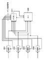
- FIG. 10 is a block diagram illustrating another modification of the receiving system in FIG. 3.
- FIG. 10 is a block diagram showing still another modification of the receiving system in FIG. 3.
- FIG. 7 is a timing diagram for explaining the operation of the reception system of FIG. 6.
- FIG. 10 is a block diagram showing still another modification of the receiving system in FIG. 3. It is a block diagram which shows the detailed structural example of the add-on part in FIG.
- FIG. 10 is a block diagram showing still another modification of the receiving system in FIG. 3.
- FIG. 10 is a block diagram showing still another modification of the receiving system in FIG. 3.
- FIG. 14 is a timing chart for explaining the operation of the reception system of FIG. 13.
- FIG. 10 is a block diagram showing still another modification of the receiving system in FIG. 3.
- FIG. 16 is a timing diagram for explaining the operation of the reception system of FIG. 15.
- FIG. 16 is a timing chart for explaining detailed operation of the reception system of FIG. 15.
- FIG. 10 is a block diagram showing still another modification of the receiving system in FIG. 3.
- FIG. 10 is a block diagram showing still another modification of the receiving system in FIG. 3.
- FIG. 10 is a block diagram showing still another modification of the receiving system in FIG. 3. It is a block diagram which shows the structure of the receiving system which concerns on 2nd Embodiment.
- (A) is a block diagram which shows the modification of the receiving system of FIG. 20, (b) is a timing diagram for demonstrating the operation
- (A) is a block diagram which shows the other modification of the receiving system of FIG. 20, (b) is a timing diagram for demonstrating the operation
- (A) is a block diagram which shows the other modification of the receiving system of FIG. 20, (b) is a timing diagram for demonstrating the operation
- (A) is a block diagram which shows the other modification of the receiving system of FIG. 20, (b) is a timing diagram for demonstrating the operation
- FIG. 21 is a block diagram illustrating still another modification of the reception system in FIG. 20. It is a block diagram which shows the structure of the transmission system which concerns on 3rd Embodiment. It is a block diagram which shows the structure of the receiving system which concerns on 3rd Embodiment.
- (A) And (b) is a timing diagram for demonstrating operation
- FIG. 31 is a timing diagram illustrating a configuration example of reception data of the reception system in FIG. 30.
- FIG. 31 is a timing chart for explaining another operation of the reception system of FIG. 30. It is a timing diagram for demonstrating a certain operation
- FIG. 36 is a timing chart showing first exception processing in the data configuration of FIG. 35.
- FIG. 36 is a timing chart showing second exception handling in the data configuration of FIG. 35.
- FIG. 36 is a timing chart showing third exception handling in the data configuration of FIG. 35.
- FIG. 36 is a timing chart showing fourth exception processing in the data configuration of FIG. 35.
- FIG. 1 is a block diagram illustrating a configuration of a transmission / reception system according to the present disclosure.
- the transmission / reception system of FIG. 1 is a multi-carrier transmission / reception system for transmitting image and audio data related to CATV, and includes a transmitter 100, a CATV transmission path 150, a receiver 200, and a back-end processing unit. 300.
- the transmitter 100 includes a dividing unit 110 and a plurality of modulation units 121, 122, 123, and 124 so as to configure a transmission system that divides one input signal and outputs a plurality of transmission signals.
- the dividing unit 110 divides one input signal (a stream exceeding the transmission capacity of one carrier wave) into a plurality of signals and outputs the signals.
- Each of the modulation units 121 to 124 employs a modulation scheme of either 256QAM (Quadrature Amplitude Modulation) or 64QAM.
- the receiver 200 includes a plurality of demodulation units 201, 202, 203, 204 and a synthesis unit 210.
- Demodulating sections 201-204 demodulate signals received via CATV transmission line 150, respectively, using a demodulation scheme corresponding to modulating sections 121-124.
- the combining unit 210 generates one stream based on the outputs of the demodulation units 201 to 204.
- the back-end processing unit 300 receives the output from the synthesis unit 210 and generates an output to a display device (not shown).
- the receiver 200 and the back-end processing unit 300 constitute a reception system that receives a plurality of carrier waves and generates one stream.
- processing for detecting headers and obtaining header information (2) processing for absorbing arrival time differences between channels, and (3) inserting dummy slots Processing for matching the data rate between the channels and (4) processing for synthesizing the data series by parallel / serial conversion are required.
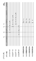
- FIG. 2 is a timing chart showing an example of a data configuration in the transmission / reception system of FIG.
- one slot (one packet) is configured with 188 bytes.
- the first byte of the slot is a synchronization byte with a fixed value (0x47), and the subsequent 3 bytes are a TS header including PID and the like.
- One frame is composed of 53 slots, and the first slot is a TSMF (Transport Stream Multiplexing Frame) header (see Patent Document 1).
- TSMF Transport Stream Multiplexing Frame
- one superframe is composed of 4 frames in 256QAM and 3 frames in 64QAM.
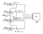
- FIG. 3 is a block diagram illustrating a configuration of the receiving system according to the first embodiment.
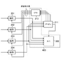
- the receiving system of FIG. 3 is obtained by adding an add-on unit 211 to an existing receiving system having a function of simultaneously processing a plurality of channels (for example, a simultaneous recording function), and includes a plurality of demodulating units 201 to 204 and an add-on unit 211. And a selector unit 212 and a back-end processing unit 300.
- the add-on unit 211 generates one stream based on the outputs of the plurality of demodulation units 201 to 204 as the synthesis unit 210 described above.
- the selector unit 212 receives the output from the demodulator unit 201 and one stream from the add-on unit 211, and selects and outputs one of them. At this time, the selector unit 212 selects the output from the demodulation unit 201 in the case of the individual carrier transmission reception mode, and selects one stream from the add-on unit 211 in the case of the multi-carrier transmission reception mode.
- the back-end processing unit 300 receives the output from the selector unit 212 and the outputs from the demodulation units 202 to 204 as input, and generates an output to the display device.
- the back-end processing unit 300 separately processes the output of the selector unit 212 and the outputs of the demodulation units 202 to 204 in the individual carrier transmission reception mode, and outputs the output of the selector unit 212 in the multi-carrier transmission reception mode. The output is processed so that the outputs of the demodulation units 202 to 204 are not processed.
- the back-end processing unit 300 can determine whether to select the individual carrier transmission reception mode or the multi-carrier transmission reception mode. For example, when a channel adopting the multi-carrier transmission method is selected by designating a channel to be viewed, the multi-carrier transmission reception mode is set.
- an add-on unit 211 that performs synthesis processing is added to an existing system, and a conventional stream and a combined stream are switched and input to one of the inputs of the back-end processing unit 300.
- a receiving system of a multi-carrier transmission system can be provided.
- the demodulation units 201 to 204, the add-on unit 211, the selector unit 212, and the back-end processing unit 300 may be realized by a single LSI (Large Scale Integrated circuit). Further, only the add-on unit 211 and the selector unit 212 may be realized by one LSI 401. Further, the add-on unit 211, the selector unit 212, and the back-end processing unit 300 may be realized by one LSI 402.
- FIG. 4 is a block diagram showing a modification of the receiving system of FIG.
- the output timings of the plurality of demodulation units 201 to 204 are adjusted by using the memories built in the plurality of demodulation units 201 to 204 to perform arrival time difference absorption and dummy slot insertion processing.
- the add-on unit 211 added as the combining unit 210 rearranges and combines the output data of the plurality of demodulation units 201 to 204.
- the idle time difference absorption and dummy slot insertion processing can be performed using the idle memory of the demodulation units 201-204.
- FIG. 5 is a block diagram showing another modification of the receiving system of FIG.
- a delay correction value is input to each of a plurality of demodulation units 201 to 204, and the output timing is adjusted using these delay correction values.
- the delay difference of the superframe caused by the difference in arrival time at the receiving system is set to 0 after delay adjustment (with a dummy slot inserted) and input to the back-end processing unit 300, so that the add-on unit 211 does not require memory. Can be downsized.
- FIG. 6 is a block diagram showing still another modification of the receiving system of FIG.
- the add-on unit 211 obtains the delay difference between the outputs of the demodulation units 201 to 204, and obtains the delay correction value of each of the demodulation units 201 to 204 based on the delay difference.
- the delay correction value input from the outside to each of the demodulation units 201 to 204 in FIG. 5 is obtained by detecting the arrival time difference of each stream by the add-on unit 211.
- FIG. 7 is a timing chart for explaining the operation of the receiving system of FIG.
- the add-on unit 211 uses the common counter for each output of the demodulation units 201 to 204 to obtain the difference in the arrival time at the head of the superframe of each channel.
- FIG. 8 is a block diagram showing still another modification of the receiving system of FIG.
- the delay correction value from the add-on unit 211 is transferred between chips via an interface such as I2C via a communication circuit such as the CPU 213.
- the CPU 213 and the back-end processing unit 300 may be realized by one LSI 403.
- FIG. 9 is a block diagram illustrating a detailed configuration example (and a part of each demodulation unit) of the add-on unit 211 in FIG.
- Each of the demodulating units 201 and 202 of FIG. 9 includes a delay adjusting unit 220, and the add-on unit 211 includes a delay time difference detecting unit 221 and a delay time difference updating unit 222 for each channel.
- the add-on unit 211 holds the first delay correction value and the second delay correction value, and when the delay difference between the outputs of the demodulating units 201 and 202 that are continuously input is greater than or equal to a preset value. Is configured to update the held first delay correction value and second delay correction value.
- FIG. 10 is a block diagram illustrating a detailed configuration example of the arrival time difference update unit 222 in FIG.
- the arrival time difference update unit 222 of FIG. 10 includes an addition unit 230, a comparison unit 231, a selector unit 232, and a D-FF 233.
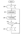
- the delay correction value X is set to 0.
- Reception processing is started, and an arrival time difference value T between channels is determined as T1.
- T1 is not 0, the value of X is updated to T1.
- each demodulation unit 201 to 204 is obtained. While the delay correction value given to is held, the fluctuation of the delay value is monitored and the delay correction value is changed when the arrival time difference changes.
- FIG. 12 is a block diagram showing still another modification of the receiving system of FIG.
- the receiving system of FIG. 12 inputs timing signals to each of the plurality of demodulation units 201 to 204, and adjusts the output timing of each using these timing signals.
- timing signals are given from the outside to the demodulation units 201 to 204, and delay adjustment is performed in the demodulation units 201 to 204 based on the timing signals.
- FIG. 13 is a block diagram showing still another modification of the receiving system of FIG.
- the receiving system in FIG. 13 inputs the same timing signal (for example, a reset signal) to the plurality of demodulation units 201 to 204, and adjusts the output timing of each using the timing signal.
- a reset signal for example, a reset signal
- a common timing signal is given to each demodulator 201-204 from the outside, and delay adjustment is performed in each demodulator 201-204 based on the timing signal.
- FIG. 14 is a timing chart for explaining the operation of the receiving system of FIG. According to FIG. 14, the add-on unit 211 obtains the arrival time (t A to t D ) of the top of the super frame in each channel with reference to the reset release time, and the difference up to a preset time (t E ) And the difference is used as a delay correction value.
- FIG. 15 is a block diagram showing still another modification of the receiving system of FIG.
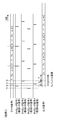
- the reception system of FIG. 15 is configured such that each of the plurality of demodulation units 201 to 204 receives timing signals from other demodulation units. That is, a timing signal for delay adjustment is generated between the demodulating units 201 to 204 and interconnected.
- FIG. 16 is a timing chart for explaining the operation of the receiving system of FIG.
- a timing signal from each of the demodulation units 201 to 204 a 1-bit signal to be asserted at the head of the super frame is shown.
- FIG. 17 is a timing chart for explaining the detailed operation of the receiving system of FIG.
- the demodulation unit 201 the latest time t D and difference value obtained by adding a fixed delay time alpha between the time t B of the self-timing signal of the timing signal (t D -t B) + ⁇ a delay correction value To do.
- ⁇ represents, for example, the time required from the start of processing by the demodulating unit until a valid output is output.
- FIG. 18 is a block diagram showing still another modification of the receiving system of FIG.
- an add-on unit 211 generates timing signals of the demodulating units 201 to 204.
- the add-on unit 211 detects the arrival time difference of each stream, and the add-on unit 211 outputs a timing signal for each of the demodulating units 201 to 204. Input to the end processing unit 300. Thereby, the add-on unit 211 does not require a memory and can be miniaturized.
- FIG. 19 is a block diagram showing still another modification of the receiving system of FIG.
- the reception system of FIG. 19 includes a memory control signal connection for the add-on unit 211 to access the demodulation units 201 to 204 between the add-on unit 211 and the demodulation units 201 to 204.
- the add-on unit 211 does not require a memory and can be miniaturized.
- FIG. 20 is a block diagram illustrating a configuration of a reception system according to the second embodiment.
- the demodulating sections 201 to 204 sequentially combine and generate a combined stream.
- the back-end processing unit 300 individually processes the outputs of the demodulation units 201 to 204 in the individual carrier transmission reception mode, and processes only the combined stream from the demodulation unit 204 in the multi-carrier transmission reception mode.
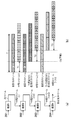
- FIG. 21 (a) is a block diagram showing a modification of the receiving system of FIG. 20, and FIG. 21 (b) is a timing diagram for explaining its operation.
- the plurality of demodulation units 201 to 204 increase the data rate step by step along the combination order.
- Various variations can be made depending on the order of synthesis, the presence or absence of a dummy slot (D) of a 64QAM stream, and the like.
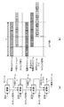
- FIG. 22 (a) is a block diagram showing another modification of the receiving system of FIG. 20, and FIG. 22 (b) is a timing diagram for explaining its operation.
- a plurality of demodulating units 201 to 204 increase the data rate of the first demodulating unit 201 to the data rate of the last demodulating unit 204, and pad the dummy slot (D) where data is insufficient, I will replace it.
- D dummy slot
- various variations can be made depending on the combination order, the presence / absence of a dummy slot (D) of a 64QAM stream, and the like.
- FIG. 23 (a) is a block diagram showing still another modification of the receiving system of FIG. 20, and FIG. 23 (b) is a timing diagram for explaining the operation thereof.
- a plurality of demodulation units 201 to 204 share each processing delay value embedded at the time of system design, or share each processing delay value by exchanging signals. Delay processing corresponding to the value is performed.
- the treatment delay value of the demodulation unit 201 is T1
- the treatment delay value of the demodulation unit 202 is T2
- the treatment delay value of the demodulation unit 203 is T3.
- the processing delay value is shared between the demodulating units 201 to 204, and each demodulating unit 201 to 204 performs a delay process corresponding thereto.
- Each processing delay value may be set from the outside of the demodulation units 201 to 204.
- FIG. 24A is a block diagram showing still another modification of the receiving system of FIG. 20, and FIG. 24B is a timing diagram for explaining the operation thereof.
- the demodulation units 201 to 203 output timing signals indicating processing start timings to the subsequent demodulation units 202 to 204.
- the arrival time difference absorption is realized by adding a timing signal synchronized with the data.
- FIG. 25 (a) is a block diagram showing still another modification of the receiving system of FIG. 20, and FIG. 25 (b) is a timing diagram for explaining the operation.
- the demodulating units 202 to 204 observe a predetermined data string (for example, a TSMF header) in the data from the preceding demodulating units 201 to 203, the processing is started.
- a predetermined data string for example, a TSMF header
- absorption of the arrival time difference is realized by inserting a known data series into the stream and using it as a reference for timing synchronization.
- FIG. 26 is a block diagram showing still another modification of the receiving system of FIG.
- the sequential processing of the demodulating units 201 and 202 and the processing of the demodulating unit 204 are performed in parallel, and then the demodulating unit 203 combines them into one combined stream. That is, the demodulating units 201 to 204 synthesize in the tournament format to generate a post-synthesis stream.
- FIG. 27 is a block diagram illustrating a configuration of a transmission system according to the third embodiment.
- the transmitter 100 in this transmission system includes a dividing unit 110, one identification data adding unit 130, and a plurality of modulating units 131 and 132.
- the dividing unit 110 divides one input signal into a plurality of signals and outputs the signals.
- the identification data adding unit 130 adds identification data (index number) to a predetermined group (superframe) of the divided signals among the signals divided by the dividing unit 110.
- Each of the modulation units 131 and 132 processes the divided signal to which the identification data is added, and outputs a transmission signal.
- the identification data may be the same data for a predetermined group, or may be different data for each divided data based on a rule shared in advance with the receiving side for the predetermined group.
- the index number of the added superframe is included in the header information.
- FIG. 28 is a block diagram showing a configuration of a receiving system according to the third embodiment.
- the receiver 200 in this reception system includes a plurality of demodulation units 201 and 202, one identification data detection unit 250, one delay correction signal generation unit 253, a plurality of delay adjustment units 261 and 262, and one combination.
- the identification data detection unit 250 identifies identification data (index number) added to a predetermined group (superframe) of the outputs of the demodulation units 201 and 202.
- the delay correction signal generation unit 253 generates a delay correction signal for the outputs of the demodulation units 201 and 202 using the detection result of the identification data detection unit 250.
- Each delay adjustment unit 261, 262 delays the output of each demodulation unit 201, 202 based on each delay correction signal and outputs a signal after delay adjustment.
- the combining unit 210 generates at least one stream based on each delay adjusted signal.
- 29 (a) and 29 (b) are timing charts for explaining the operation of the transmission / reception system of FIGS. 27 and 28.
- FIG. 29 (a) by using the index number of the superframe for delay adjustment, as shown in FIG. 29 (a), it is possible to absorb the arrival time difference exceeding one superframe period. Further, as shown in FIG. 29B, it is of course possible to reliably absorb the arrival time difference within one superframe period.
- the header number is not limited to the superframe index number as long as the header information can generate a timing signal having a longer cycle than the superframe, which is the minimum unit of synthesis.
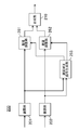
- FIG. 30 is a block diagram showing a modification of the receiving system of FIG. 30 includes a plurality of demodulation units 201 and 202, one delay correction signal generation unit 253, a plurality of delay adjustment units 261 and 262, and one synthesis unit 210.
- the delay correction signal generation unit 253 generates delay correction signals for the outputs of the demodulation units 201 and 202 using the outputs of the demodulation units 201 and 202.
- Each delay adjustment unit 261, 262 delays the output of each demodulation unit 201, 202 based on each delay correction signal, and outputs a signal after delay adjustment.
- the combining unit 210 generates at least one stream based on each delay adjusted signal.
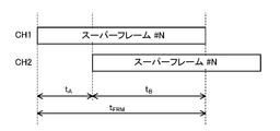
- the delay correction signal generation unit 253 obtains a delay difference between the data output from the demodulation units 201 and 202, and the delay difference is smaller than a predetermined delay amount (1/2 of one superframe period). Only the delay correction signal is generated. That is, the receiver 200 assumes that the delay difference is always within 1 ⁇ 2 of one superframe period, and processes the arrival time difference absorption as a pair to be time-adjusted at the heads of the superframes that meet the condition. I do.
- FIG. 31 is a timing chart for explaining the operation of the reception system of FIG.
- N is an arbitrary natural number
- one superframe period is t FRM
- the delay difference between the Nth superframe of channel 1 and the Nth superframe of channel 2 is t A
- the arrival time difference within 1/2 of one superframe period can be absorbed 100% with certainty.
- an index indicating data continuity (for example, in the TS packet header)
- the combination of divided data may be determined based on CC (Continuity Counter).
- FIG. 32 is a timing chart showing a configuration example of reception data of the reception system of FIG.
- the TS packet header includes a 4-bit CC that is incremented for each packet by PID.
- FIG. 33 is a timing chart for explaining the operation using CC in the receiving system of FIG.
- the combining unit 210 in FIG. 1 sorts and combines the output data of the demodulating units 201 to 204 with the header obtained from the outputs of the demodulating units 201 to 204. This may be performed based on information and information in an updatable storage unit (register) in the synthesis unit 210 that is information for interpreting the header information. Thereby, the composition order can be arbitrarily set by the register.
- the carrier sequence information that can be used here means information for identifying a carrier wave, which is, for example, 8-bit information obtained from an output obtained by demodulating a plurality of carrier waves in the receiver 200, and includes header information of an extended portion. include.
- the combining order may be determined by the magnitude of the carrier sequence information, or information for converting the carrier sequence information into the order is stored in the above register, and the combining is performed from the carrier sequence information and the register information.
- the order may be determined. It is assumed that the order determination method is shared in advance between the transmission side and the reception side.
- the combining unit 210 in FIG. 1 combines and rearranges the data output from the demodulation units 201 to 204 based on an index indicating data continuity (for example, the value of CC in the TS packet header). It may be done.
- the combining unit 210 confirms the CC and automatically determines the combining order.
- FIG. 34 is a timing chart for explaining an example of the CC use operation of the receiving system in FIG.
- the continuity of CC is confirmed because only the channel 2 has a different PID. Cannot be determined.
- the PID of all channels is the same, so the continuity of CC can be confirmed.
- the arrangement of the carrier waves is in the order of channel 3, channel 1, channel 4, and channel 2.
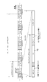
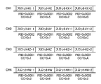
- FIG. 35 is a timing diagram illustrating an example of a data configuration in the transmission / reception system according to the fourth embodiment.
- transmission / reception is performed after converting a variable-length TLV (Types Length Value) packet into a fixed-length transmission packet.
- TLV Types Length Value
- the transmission packet has a fixed packet length of 188 bytes, the first 3 bytes are a header (that is, a divided TLV packet header), and the subsequent 185 bytes are a payload.
- the TLV packet start indicator in the divided TLV packet header is “1”, it indicates that the head of the TLV packet is included in the payload of this divided TLV packet.
- the head TLV instruction is the first byte of the payload used when the TLV packet start indicator is “1”, and indicates the number of bytes of the payload where the head position of the TLV packet is based on the value of the head TLV instruction. When the TLV packet start indicator is “0”, the head TLV instruction is not inserted.
- the variable length to be assigned next In the data allocation method in which head position information (head TLV instruction) indicating the start position of packet 2 which is a packet is inserted and packet 2 is continuously allocated, after the allocation of packet 1 ends in the middle of the transmission packet, the next If the start position information (start TLV instruction) indicating the start position of the packet 2 to be assigned to is inserted, the packet 2 may not be assigned. In the fourth embodiment, exception processing in such a case will be described.
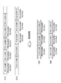
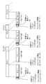
- FIG. 36 is a timing chart showing a first exception process in the data configuration of FIG.
- the leading position information (the leading TLV instruction) indicating the starting position of the packet 2 to be allocated next
- the head TLV instruction enters the next transmission packet.
- variable length packet 1 is set so as to acquire the variable length TLV packet allocated to the fixed length transmission packet. Acquisition of the data to be configured ends in the fixed-length transmission packet 1, and the start position information (start TLV instruction) indicating the start position of the next variable-length packet 2 is inserted in the fixed-length transmission packet 1. If not, data other than the data constituting the variable-length packet 1 in the fixed-length transmission packet 1 is treated as invalid data.
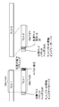
- FIG. 37 is a timing chart showing second exception processing in the data configuration of FIG.
- the leading position information (the leading TLV instruction) indicating the starting position of the packet 2 to be allocated next If the packet 2 cannot be assigned by inserting, an invalid value is substituted for the head position information (head TLV instruction). That is, the field after 184 that does not actually exist is designated by the head TLV instruction.
- variable length packet 1 is set so as to acquire the variable length TLV packet allocated to the fixed length transmission packet.
- Acquisition of the data to be configured ends in the fixed-length transmission packet 1, and in the fixed-length transmission packet 1, the start position information (start TLV instruction) indicating the start position of the next variable-length packet 2 is added to the start position.
- start TLV instruction When an invalid value is substituted as information (head TLV instruction), processing is performed assuming that data constituting the variable-length packet 2 does not exist in the fixed-length transmission packet 1.
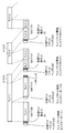
- FIG. 38 is a timing chart showing third exception processing in the data configuration of FIG.
- the transmission packet includes the beginning of a variable-length TLV packet
- the head position information head TLV instruction
- the variable-length TLV packet When the head is not included, invalid data is inserted instead of the head position information (head TLV instruction). That is, when the TLV packet start indicator is “0”, 1 byte at an arbitrary position is padded to make the actual payload length 184 bytes.
- variable length packet 1 is acquired so as to acquire the variable length TLV packet allocated to the fixed length transmission packet.
- start position information start TLV instruction
- start position 2 of the next variable-length packet 2 is not included in the fixed-length transmission packet 1
- the transmission packet 1 is processed by determining that invalid data is included in addition to the data constituting the variable-length packet 1.
- FIG. 39 is a timing chart showing a fourth exception process in the data structure of FIG.
- the start position of the packet 2 to be allocated next to the head position information (head TLV instruction) is determined.
- the value shown is substituted, and when the beginning of the variable-length TLV packet is not included, an invalid value is substituted for the head position information (head TLV instruction). That is, when the payload length of the divided TLV packet is fixed to 184 bytes and the head TLV instruction is always inserted and the head of the TLV packet is not included, an invalid pointer position (for example, invalid value Z) is set to the head TLV. Substitute for instructions.
- the variable length packet 1 is acquired so as to acquire the variable length TLV packet allocated to the fixed length transmission packet.
- the start position information (start TLV instruction) indicating the start position 2 of the next variable-length packet 2 is invalid as the start position information (start TLV instruction). If a variable value is assigned, all the data to which the data constituting the variable-length packet in the fixed-length transmission packet 1 is assigned is determined to be data constituting the variable-length packet 1 and processed.
- a head TLV instruction area is secured in the payload separately from the divided TLV packet header.
- the TLV packet start indicator and the head TLV instruction area are separated by arranging the head TLV instruction area that is supposed to be present in the payload in the divided TLV packet header. Both may be present in the split TLV packet header.
- the head TLV instruction area is arranged at the head of the divided TLV packet header, there is an effect that the latency from the data reception to the processing end is shortened in the processing in the receiver 200 or the back-end processing unit 300.
- the divided TLV packet header may be considered as 4 bytes, or the extra 1 byte is deleted from the portion excluding the TLV packet start indicator and the head TLV instruction area, and the divided TLV packet header is changed to 3 bytes. It may be left as it is.
- the above-described data arrangement may be provided only between the receiver 200 and the back-end processing unit 300. That is, after the receiver 200 reconstructs the variable-length data sequence from the fixed-length packet data sequence, both the TLV packet start indicator and the head TLV instruction area are arranged in the divided TLV packet header, and in particular, the head TLV.
- the receiver 200 may perform a process of arranging the instruction area at the head of the divided TLV packet header.
- the method is not limited to TSMF, and the modulation method is not limited to QAM.
- the stream format is not limited to TS packets or TLV packets.
- the number of carrier waves is not limited to four or two.
- each demodulator 201-204 is not limited to an IF (intermediate frequency) signal, but may be an RF (high frequency) signal or data after analog-digital conversion.
- Each demodulator 201 to 204 may output a plurality of streams in the TS packet format.
- Information passed from the add-on unit 211 to the demodulation units 201 to 204 is not limited to the delay correction value and the timing signal.
- the data transmission path is not limited to the CATV transmission path 150 in FIG.
- Transmission data is not limited to image and audio data. Any scheme that divides and transmits a stream exceeding the transmission capacity of one carrier into a plurality of carriers is not limited to the multiple carrier transmission scheme.
- the multi-level number of modulation is not limited to 64 and 256.
- the packet configuration is not limited to the above configuration.
- the add-on unit 211 is added to an existing reception system having a simultaneous recording function of a plurality of channels.
- the present invention is not limited to this as long as the system receives a plurality of different channels simultaneously. .
- the transmission / reception system according to the present disclosure is useful as a transmission / reception system of a multi-carrier transmission scheme.
Landscapes
- Engineering & Computer Science (AREA)
- Signal Processing (AREA)
- Computer Networks & Wireless Communication (AREA)
- Power Engineering (AREA)
- Two-Way Televisions, Distribution Of Moving Picture Or The Like (AREA)
- Time-Division Multiplex Systems (AREA)
- Computer Security & Cryptography (AREA)
- Transceivers (AREA)
- Digital Transmission Methods That Use Modulated Carrier Waves (AREA)
- Synchronisation In Digital Transmission Systems (AREA)
Abstract
Description
図3は、第1の実施形態に係る受信システムの構成を示すブロック図である。図3の受信システムは、複数チャンネルを同時に処理する機能(例えば同時録画機能)を有する既存の受信システムにアドオン部211を付加したものであって、複数の復調部201~204と、アドオン部211と、セレクタ部212と、バックエンド処理部300とを備えている。アドオン部211は、前述の合成部210として、複数の復調部201~204の出力に基づいて1つのストリームを生成する。セレクタ部212は、復調部201からの出力と、アドオン部211からの1つのストリームとを入力とし、いずれか一方を選択して出力する。この際、セレクタ部212は、個別搬送波伝送受信モードの場合には復調部201からの出力を選択し、複数搬送波伝送受信モードの場合にはアドオン部211からの1つのストリームを選択する。バックエンド処理部300は、セレクタ部212からの出力と、復調部202~204からの出力とを入力とし、表示装置への出力を生成する。
図20は、第2の実施形態に係る受信システムの構成を示すブロック図である。図20の受信システムは、各復調部201~204で順次合成して、合成後ストリームを生成するものである。バックエンド処理部300は、個別搬送波伝送受信モードでは復調部201~204の出力を個別に処理し、複数搬送波伝送受信モードでは復調部204からの合成後ストリームのみを処理する。
図27は、第3の実施形態に係る送信システムの構成を示すブロック図である。この送信システムにおける送信機100は、分割部110と、1つの識別データ付加部130と、複数の変調部131,132とを備える。分割部110は、1つの入力信号を複数の信号に分割して出力する。識別データ付加部130は、分割部110で分割された信号のうちの分割後信号の所定のグループ(スーパーフレーム)に対して識別データ(インデックス番号)を付加する。各変調部131,132は、識別データが付加された分割後信号をそれぞれ処理して送信信号を出力する。識別データは所定のグループに同一のデータであってもよいし、もしくは所定のグループに対し、予め受信側と共有された法則に基づいてそれぞれの分割データ毎に異なったデータであってもよい。付加されたスーパーフレームのインデックス番号は、ヘッダ情報に含まれる。
図35は、第4の実施形態に係る送受信システムにおけるデータ構成の例を示すタイミング図である。ここでは、可変長のTLV(Types Length Value)パケットを固定長の伝送パケットに変換したうえで送受信が行われるものとする。
以上のように、本出願において開示する技術の例示として、第1~第4の実施形態を説明した。しかしながら、本開示における技術は、これらに限定されず、適宜、変更、置き換え、付加、省略、順番の入れ替え等を行った実施形態にも適用可能である。また、上記実施形態で説明した各構成要素を組み合わせて、新たな実施形態とすることも可能である。
110 分割部
121~124 変調部
130 識別データ付加部
131,132 変調部
200 受信機
201~204 復調部
210 合成部
211 アドオン部
212 セレクタ部
213 CPU
220 遅延調整部
221 遅延時間差検出部
222 遅延時間差更新部
250 識別データ検出部
253 遅延補正信号生成部
261,262 遅延調整部
300 バックエンド部
401~403 LSI
Claims (43)
- 複数の搬送波を受信し、1つあるいは複数のストリームを生成する受信システムであって、
第1の送信信号を受信して処理する第1の復調部と、
前記第1の送信信号とは異なる第2の送信信号を受信して処理する第2の復調部と、
少なくとも前記第1の復調部の出力と前記第2の復調部の出力とに基づいて、1つのストリームを生成する合成部と、
前記第1の復調部からの出力と、前記合成部からの前記1つのストリームとを入力とし、いずれか一方を選択して出力するセレクタ部と、
前記セレクタ部からの出力と、前記第2の復調部からの出力とを入力とし、表示装置への出力を生成するバックエンド処理部とを備え、
前記セレクタ部は、個別搬送波伝送受信モードの場合には、前記第1の復調部の出力を選択し、複数搬送波伝送受信モードの場合には、前記1つのストリームを選択することを特徴とする受信システム。 - 請求項1記載の受信システムにおいて、
前記第1の復調部と、前記第2の復調部と、前記合成部と、前記セレクタ部と、前記バックエンド処理部とが1つのLSIで実現されたことを特徴とする受信システム。 - 請求項1記載の受信システムにおいて、
前記合成部と、前記セレクタ部と、前記バックエンド処理部とが1つのLSIで実現されたことを特徴とする受信システム。 - 請求項1記載の受信システムにおいて、
前記合成部と、前記セレクタ部とが1つのLSIで実現されたことを特徴とする受信システム。 - 請求項1記載の受信システムにおいて、
前記バックエンド処理部は、前記個別搬送波伝送受信モードのときには、前記セレクタ部の出力と、前記第2の復調部の出力とを別々に処理し、前記複数搬送波伝送受信モードのときには、前記セレクタ部の出力を処理し、前記第2の復調部の出力を処理しないことを特徴とする受信システム。 - 請求項1記載の受信システムにおいて、
前記バックエンド処理部は、前記個別搬送波伝送受信モードか前記複数搬送波伝送受信モードかのいずれを選択するかを決定することを特徴とする受信システム。 - 複数の搬送波を受信し、1つあるいは複数のストリームを生成する受信システムであって
第1の送信信号を受信して処理する第1のメモリを内蔵する第1の復調部と、
前記第1の送信信号とは異なる第2の送信信号を受信して処理する第2のメモリを内蔵する第2の復調部と、
少なくとも前記第1の復調部の出力と前記第2の復調部の出力とに基づいて、1つのストリームを生成する合成部と、
前記第1のメモリと、前記第2のメモリを使用することにより、前記第1の復調部の出力のタイミングと、前記第2の復調部の出力のタイミングとを調整し、前記合成部では、前記第1の復調部の出力のデータと前記第2の復調部の出力のデータとの並べ替えと結合とを行うことを特徴とする受信システム。 - 請求項7記載の受信システムにおいて、
前記第1の復調部に第1の遅延補正値を入力し、前記第2の復調部に第2の遅延補正値を入力し、前記第1の遅延補正値と前記第2の遅延補正値とを使用して、それぞれの出力タイミングを調整することを特徴とする受信システム。 - 請求項8記載の受信システムにおいて、
前記合成部は、前記第1の復調部の出力と、前記第2の復調部の出力との遅延差を求め、前記遅延差に基づき、前記第1の遅延補正値と前記第2の遅延補正値とを求めることを特徴とする受信システム。 - 請求項9記載の受信システムにおいて、
前記合成部は、前記第1の遅延補正値と前記第2の遅延補正値とを保持し、引き続き入力される前記第1の復調部の出力と前記第2の復調部の出力との遅延差が、以前に求めた遅延差から、予め設定した値以上に変化した場合には、保持している前記第1の遅延補正値と前記第2の遅延補正値とを更新することを特徴とする受信システム。 - 請求項7記載の受信システムにおいて、
前記第1の復調部に第1のタイミング信号を入力し、前記第2の復調部に第2のタイミング信号を入力し、前記第1のタイミング信号と前記第2のタイミング信号とを使用して、それぞれの出力タイミングを調整することを特徴とする受信システム。 - 請求項11記載の受信システムにおいて、
前記第1のタイミング信号と前記第2のタイミング信号とは同一の信号であることを特徴とする受信システム。 - 請求項11記載の受信システムにおいて、
前記第1のタイミング信号は前記第2の復調部が生成し、前記第2のタイミング信号は前記第1の復調部が生成することを特徴とする受信システム。 - 請求項11記載の受信システムにおいて、
前記合成部は、前記第1のタイミング信号と前記第2のタイミング信号とを生成することを特徴とする受信システム。 - 複数の搬送波を受信し、1つあるいは複数のストリームを生成する受信システムであって、
第1の送信信号を受信して処理する第1のメモリを内蔵する第1の復調部と、
前記第1の送信信号とは異なる第2の送信信号を受信して処理する第2のメモリを内蔵する第2の復調部と、
少なくとも前記第1の復調部の出力と前記第2の復調部の出力とに基づいて、1つのストリームを生成する合成部と、
前記合成部からの出力を入力とし、表示装置への出力を生成するバックエンド処理部とを備え、
前記合成部と、前記第1の復調部及び前記第2の復調部との間には、前記合成部が前記第1のメモリと前記第2のメモリとにアクセスするための、メモリ制御信号の接続を備えることを特徴とする受信システム。 - 複数の搬送波を受信し、1つあるいは複数のストリームを生成する受信システムであって、
第1の送信信号を受信して処理する第1のメモリを内蔵する第1の復調部と、
前記第1の送信信号とは異なる第2の送信信号を受信して処理する第2のメモリを内蔵する第2の復調部と、
少なくとも前記第1の復調部の出力と前記第2の復調部の出力とに基づいて、1つのストリームを生成する合成部と、
前記合成部からの出力を入力とし、表示装置への出力を生成する、第3のメモリを内蔵するバックエンド処理部とを備え、
前記合成部と、前記第1の復調部及び前記第2の復調部及び前記バックエンド処理部のうち少なくとも1つとの間には、前記合成部が前記第1のメモリと前記第2のメモリと前記第3のメモリとのうち少なくとも1つにアクセスするための、メモリ制御信号の接続を備えることを特徴とする受信システム。 - 複数の搬送波を受信し、1つあるいは複数のストリームを生成する受信システムであって、
第1の送信信号を受信して処理する第1のメモリを内蔵する第1の復調部と、
前記第1の送信信号とは異なる第2の送信信号を受信し処理する第2のメモリを内蔵する第2の復調部と、
更に1以上の復調部と、
表示装置への出力を生成するバックエンド処理部とを備え、
前記第1の復調部と、前記第2の復調部とを含む複数の復調部は、前記複数の復調部全てを接続する直列接続を含み、
前記複数の復調部を、第1の搬送波のデータを受信し、他の復調部で復調したデータを入力しない先頭の復調部と、第2の搬送波のデータを受信し、復調した結果を少なくとも前記バックエンド処理部への出力の一部とする最後の復調部と、前記先頭の復調部及び前記最後の復調部以外の中間の復調部とに分類したとき、
前記先頭の復調部は、出力を前記中間の復調部の1つの復調部に出力し、前記中間の復調部のそれぞれは、それぞれに対応する搬送波のデータを復調した結果と、前段の復調部の出力との両方を、後段の復調部へストリームの一部として出力することを特徴とする受信システム。 - 請求項17記載の受信システムにおいて、
前記複数の復調部は、結合順序に沿って段階的にデータレートを上げていくことを特徴とする受信システム。 - 請求項17記載の受信システムにおいて、
前記複数の復調部は、前記先頭の復調部で前記最後の復調部のデータレートまで上げて、データが不足するところは無効データを配置しておき、順次データを置き換えていくことを特徴とする受信システム。 - 請求項17記載の受信システムにおいて、
前記複数の復調部は、システム設計時に予め設定された各々の処理遅延の値を互いに共有し、各復調部で当該値に対応した遅延処理を行うことを特徴とする受信システム。 - 請求項17記載の受信システムにおいて、
前記中間の復調部及び最後の復調部は、各復調部で行う遅延処理の設定を各復調部の外部から行うことを特徴とする受信システム。 - 請求項17記載の受信システムにおいて、
前記複数の復調部は、信号のやり取りで各々の処理遅延の値を共有し、各復調部で当該値に対応した遅延処理を行うことを特徴とする受信システム。 - 請求項17記載の受信システムにおいて、
先頭の復調部及び中間の復調部は、後段の復調部に対して、処理開始タイミングを示すタイミング信号を出力することを特徴とする受信システム。 - 請求項17記載の受信システムにおいて、
中間の復調部及び最後の復調部は、前段の復調部からのデータ中の所定のデータ列を観測すると、処理を開始することを特徴とする受信システム。 - 1つの入力信号を分割し、複数の送信信号を出力する送信システムであって、
1つの入力信号を複数の信号に分割して出力する分割部と、
前記分割部で分割された信号のうちの分割後信号の所定のグループに対して識別データを付加する識別データ付加部と、
前記識別データが付加された第1分割後信号を処理して第1送信信号を出力する第1変調部と、
前記識別データが付加された第2分割後信号を処理して第2送信信号を出力する第2変調部とを備えたことを特徴とする送信システム。 - 複数の搬送波を受信し、1つのストリームを生成する受信システムであって、
第1の送信信号を受信して処理する第1の復調部と、
前記第1の送信信号とは異なる第2の送信信号を受信し処理する第2の復調部と、
前記第1の復調部の出力と前記第2の復調部の出力とを入力とし、前記第1の復調部の出力と前記第2の復調部の出力に含まれる所定の識別データを識別する識別データ検出部と、
前記識別データ検出部の識別結果に基づいて所定の方法で前記第1の復調部の出力と前記第2の復調部の出力との時間差を調整する対象を決定する遅延補正信号生成部とを備えたことを特徴とする受信システム。 - 請求項26記載の受信システムにおいて、
前記所定の識別データとは、前記第1の復調部の出力の所定のグループに対して付加された第1の識別データと、前記第2の復調部の出力の所定のグループに対して付加された第2の識別データであり、
前記所定の処理とは、前記第1の識別データの識別データ1と前記識別データ1に対応する前記第2の識別データの識別データ2との時間差を検出することを特徴とする受信システム。 - 請求項26記載の受信システムにおいて、
前記所定の識別データとは、前記第1の復調部の出力の所定のグループの先頭を示す第1先頭情報と、前記第2の復調部の出力の所定のグループの先頭を示す第2先頭情報であり、
前記所定の処理とは、前記第1先頭情報と第2先頭情報との第1の時間差を検出し、前記時間差が所定の値よりも小さい場合にのみ、時間差を調整する対象とすることを特徴とする受信システム。 - 請求項26記載の受信システムにおいて、
前記ストリームは、パケット内にデータの連続性を示す指標が存在する複数のパケットから構成されるストリームであって、
前記所定の識別データとは、前記データの連続性を示す指標であり、
前記所定の処理とは、前記データの連続性を示す指標の並びに基づいて時間差を調整する対象を決定することを特徴とする受信システム。 - 複数の搬送波を受信し、1つのストリームを生成する受信システムであって、
第1の送信信号を受信して処理する第1の復調部と、
前記第1の送信信号とは異なる第2の送信信号を受信し処理する第2の復調部と、
少なくとも前記第1の復調部の出力と前記第2の復調部の出力とに基づいて、1つのストリームを生成する合成部とを備え、
前記合成部では、前記第1の復調部の出力のデータと前記第2の復調部の出力のデータとの並べ替えと結合とを行い、前記並べ替えと結合とは、所定の識別データに基づいて行うことを特徴とする受信システム。 - 請求項30記載の受信システムにおいて、
前記所定の識別データとは、前記合成部中の更新可能な記憶部内の情報であることを特徴とする受信システム。 - 請求項30記載の受信システムにおいて、
前記ストリームは、パケット内にデータの連続性を示す指標が存在する複数のパケットから構成されるストリームであって、
前記所定の識別データとは、前記データの連続性を示す指標であることを特徴とする受信システム。 - 可変長パケットのデータを分割し、固定長の伝送パケットに割り当てていく際に、可変長パケット1の割り当てが固定長の伝送パケット1の途中で終了した場合には、次に割り当てる可変長パケット2の開始位置を示す先頭位置情報を前記伝送パケット1に挿入し、続けて前記可変長パケット2を割り当てていくデータ割り当て方法であって、
前記可変長パケット1の割り当てが前記伝送パケット1の途中で終わった後に、次に割り当てる前記可変長パケット2の開始位置を示す先頭位置情報1を挿入すると、前記伝送パケット1に前記可変長パケット2の割り当てを行えない場合には、前記伝送パケット1に、前記先頭位置情報1の代わりに、無効なデータを割り当てることを特徴とするデータ割り当て方法。 - 請求項33記載のデータ割り当て方法において、
前記無効なデータとは、先頭位置情報として無効な値を代入された先頭位置情報であることを特徴とするデータ割り当て方法。 - 固定長の伝送パケットに割り当てられている可変長パケットを取得するデータ取得方法であって、
可変長パケット1を構成するデータの取得が固定長の伝送パケット1内で終わり、かつ、前記固定長の伝送パケット1内に、次の可変長パケット2の開始位置を示す先頭位置情報が挿入されていない場合には、固定長の前記伝送パケット1には、前記可変長パケット1を構成するデータの他に、無効なデータが含まれていると判断して処理することを特徴とするデータ取得方法。 - 請求項35記載のデータ取得方法において、
前記次の可変長パケット2の開始位置を示す先頭位置情報が挿入されていない場合とは、前記無効なデータが、先頭位置情報として無効な値が代入されている前記先頭位置情報であることを特徴とするデータ取得方法。 - 可変長パケットのデータを分割し、固定長の伝送パケットに割り当てていく際に、可変長パケット1の割り当てが伝送パケット1の途中で終了した場合には、次に割り当てる可変長パケット2の開始位置を示す先頭位置情報を前記伝送パケット1に挿入し、続けて前記可変長パケット2を割り当てていくデータ割り当て方法であって、
伝送パケットに可変長パケットの先頭が含まれないときは、先頭位置情報の代わりに無効なデータを割り当てることを特徴とするデータ割り当て方法。 - 請求項37記載のデータ割り当て方法において、
前記無効なデータとは、先頭位置情報として無効な値を代入された先頭位置情報であることを特徴とするデータ割り当て方法。 - 固定長の伝送パケットに割り当てられている可変長パケットを取得するデータ取得方法であって、
可変長パケット1の取得処理を行っているときに、固定長の伝送パケット1内に、次の可変長パケット2の開始位置2を示す先頭位置情報が含まれていない場合には、固定長の伝送パケット1には、可変長パケット1を構成するデータの他に、無効なデータが含まれていると判断して処理することを特徴とするデータ取得方法。 - 請求項39記載のデータ取得方法において、
前記次の可変長パケット2の開始位置を示す先頭位置情報が挿入されていない場合とは、前記無効なデータが、先頭位置情報として無効な値が代入されている前記先頭位置情報であることを特徴とするデータ取得方法。 - 可変長パケットのデータを分割し、固定長の伝送パケットに割り当てていく際に、可変長パケット1の割り当てが伝送パケット1の途中で終了した場合には、次に割り当てる可変長パケット2の開始位置を示す先頭位置情報を前記伝送パケット1の先頭にヘッダ内情報として配置し、続けて前記可変長パケット2を割り当てていくデータ割り当て方法であって、
伝送パケットに可変長パケットの先頭が含まれないときは、先頭位置情報の代わりに無効なデータを前記伝送パケット1の先頭に配置することを特徴とするデータ割り当て方法。 - 請求項41記載のデータ割り当て方法において、
前記ヘッダは、前記可変長パケット2の先頭が前記伝送パケット1中に存在するかしないかを示すインジケーターを含むことを特徴とするデータ割り当て方法。 - 固定長の伝送パケットに割り当てられている可変長パケットを取得するデータ取得方法であって、
可変長パケット1の取得処理を行っているときに、固定長の伝送パケット1内のヘッダ中の、次の可変長パケット2の先頭位置情報が前記伝送パケット1内に存在するかしないかを示すインジケーターを参照し、前記先頭位置情報が存在することを前記インジケーターが示している場合には、前記伝送パケット1の先頭に前記先頭位置情報が配置されていると判断し、前記先頭位置情報が存在しないことを前記インジケーターが示している場合には、前記伝送パケット1の先頭には無効なデータが配置されていると判断して処理することを特徴とするデータ取得方法。
Priority Applications (5)
| Application Number | Priority Date | Filing Date | Title |
|---|---|---|---|
| JP2016570530A JP6635050B2 (ja) | 2015-01-22 | 2016-01-05 | 分割データの受信システム |
| CN201680004331.XA CN107113072B (zh) | 2015-01-22 | 2016-01-05 | 接收系统 |
| BR112017014886-2A BR112017014886B1 (pt) | 2015-01-22 | 2016-01-05 | Sistema receptor que recebe uma pluralidade de portadoras e que gera um ou uma pluralidade de fluxos e sistema receptor que recebe uma pluralidade de portadoras e que gera um fluxo |
| US15/646,849 US10225128B2 (en) | 2015-01-22 | 2017-07-11 | Divided data transmitting and receiving system |
| US16/250,579 US10601631B2 (en) | 2015-01-22 | 2019-01-17 | Divided data transmitting and receiving system |
Applications Claiming Priority (2)
| Application Number | Priority Date | Filing Date | Title |
|---|---|---|---|
| JP2015009984 | 2015-01-22 | ||
| JP2015-009984 | 2015-01-22 |
Related Child Applications (1)
| Application Number | Title | Priority Date | Filing Date |
|---|---|---|---|
| US15/646,849 Continuation US10225128B2 (en) | 2015-01-22 | 2017-07-11 | Divided data transmitting and receiving system |
Publications (1)
| Publication Number | Publication Date |
|---|---|
| WO2016117283A1 true WO2016117283A1 (ja) | 2016-07-28 |
Family
ID=56416840
Family Applications (1)
| Application Number | Title | Priority Date | Filing Date |
|---|---|---|---|
| PCT/JP2016/000023 Ceased WO2016117283A1 (ja) | 2015-01-22 | 2016-01-05 | 分割データの送受信システム |
Country Status (4)
| Country | Link |
|---|---|
| US (2) | US10225128B2 (ja) |
| JP (3) | JP6635050B2 (ja) |
| CN (2) | CN107113072B (ja) |
| WO (1) | WO2016117283A1 (ja) |
Cited By (5)
| Publication number | Priority date | Publication date | Assignee | Title |
|---|---|---|---|---|
| JP2018064139A (ja) * | 2016-10-11 | 2018-04-19 | 株式会社日立情報通信エンジニアリング | 高精細映像送信機、高精細映像受信機および高精細映像送受信システム |
| JP2018078561A (ja) * | 2016-10-31 | 2018-05-17 | 日本放送協会 | 分離装置及びチップ |
| WO2020004050A1 (ja) * | 2018-06-27 | 2020-01-02 | ソニーセミコンダクタソリューションズ株式会社 | 受信装置、及び受信方法 |
| TWI690150B (zh) * | 2017-06-14 | 2020-04-01 | 日商索尼半導體解決方案公司 | 解調裝置、處理裝置、收訊裝置、及資料處理方法 |
| KR20210023858A (ko) | 2018-06-27 | 2021-03-04 | 소니 세미컨덕터 솔루션즈 가부시키가이샤 | 수신 장치 및 수신 방법 |
Families Citing this family (7)
| Publication number | Priority date | Publication date | Assignee | Title |
|---|---|---|---|---|
| WO2016080234A1 (ja) * | 2014-11-21 | 2016-05-26 | ソニー株式会社 | 送信装置、送信方法、受信装置および受信方法 |
| WO2016117283A1 (ja) * | 2015-01-22 | 2016-07-28 | 株式会社ソシオネクスト | 分割データの送受信システム |
| CN111565644B (zh) * | 2018-01-11 | 2023-08-29 | 株式会社索思未来 | 超声波诊断装置以及超声波诊断系统 |
| US11477518B2 (en) * | 2018-01-18 | 2022-10-18 | Sony Semiconductor Solutions Corporation | Signal processing device and signal processing method |
| JP2020141256A (ja) * | 2019-02-28 | 2020-09-03 | ソニーセミコンダクタソリューションズ株式会社 | 復調回路、復調方法、送信装置 |
| JP7526025B2 (ja) | 2020-04-22 | 2024-07-31 | 日本放送協会 | 送信装置及び受信装置 |
| JP7526024B2 (ja) | 2020-04-22 | 2024-07-31 | 日本放送協会 | 送信装置及び受信装置 |
Citations (4)
| Publication number | Priority date | Publication date | Assignee | Title |
|---|---|---|---|---|
| JP2005167890A (ja) * | 2003-12-05 | 2005-06-23 | Alpine Electronics Inc | 地上波ディジタル放送受信機及び地上波ディジタル放送受信方法 |
| JP2012209675A (ja) * | 2011-03-29 | 2012-10-25 | Nippon Hoso Kyokai <Nhk> | 送信装置及び受信装置 |
| US20140211812A1 (en) * | 2013-01-31 | 2014-07-31 | Electronics And Telecommunications Research Institute | Demultiplexing apparatus, multiplexing apparatus, and multi-channel transmission and reception method using the same |
| JP2015012421A (ja) * | 2013-06-28 | 2015-01-19 | 日本放送協会 | 送信装置及び受信装置 |
Family Cites Families (12)
| Publication number | Priority date | Publication date | Assignee | Title |
|---|---|---|---|---|
| JP4688244B2 (ja) * | 1999-05-13 | 2011-05-25 | ソニー株式会社 | 信号処理装置および方法、並びにコンピュータ読み取り可能な媒体 |
| JP4647149B2 (ja) * | 2001-08-06 | 2011-03-09 | 独立行政法人情報通信研究機構 | トランスポートストリームの送信装置および受信装置 |
| JP4557548B2 (ja) * | 2002-01-02 | 2010-10-06 | ソニー エレクトロニクス インク | 部分暗号化及びパケット識別子のマッピング |
| CN103299586B (zh) * | 2007-07-05 | 2016-01-20 | 日本电信电话株式会社 | 信号块串处理方法以及信号块串处理装置 |
| US9363126B2 (en) * | 2007-12-21 | 2016-06-07 | Google Technology Holdings LLC | Method and apparatus for IFDMA receiver architecture |
| WO2010005037A1 (ja) * | 2008-07-09 | 2010-01-14 | シャープ株式会社 | 通信装置、通信システム、受信方法及び通信方法 |
| WO2011114837A1 (ja) * | 2010-03-16 | 2011-09-22 | 日本電気株式会社 | 伝送装置、伝送方法及び伝送システム |
| CN101982954B (zh) * | 2010-10-19 | 2013-07-24 | 华北水利水电大学 | 一种发电厂多载波多电量变送器 |
| JP5973746B2 (ja) | 2012-02-24 | 2016-08-23 | 日本放送協会 | 送信装置及び受信装置 |
| JP5872635B2 (ja) * | 2014-06-04 | 2016-03-01 | パナソニック株式会社 | 送信装置及び受信装置 |
| US20160142343A1 (en) * | 2014-11-13 | 2016-05-19 | Broadcom Corporation | System for Recovery in Channel Bonding |
| WO2016117283A1 (ja) * | 2015-01-22 | 2016-07-28 | 株式会社ソシオネクスト | 分割データの送受信システム |
-
2016
- 2016-01-05 WO PCT/JP2016/000023 patent/WO2016117283A1/ja not_active Ceased
- 2016-01-05 JP JP2016570530A patent/JP6635050B2/ja active Active
- 2016-01-05 CN CN201680004331.XA patent/CN107113072B/zh active Active
- 2016-01-05 CN CN201910201510.8A patent/CN109873692B/zh active Active
-
2017
- 2017-07-11 US US15/646,849 patent/US10225128B2/en active Active
-
2019
- 2019-01-17 US US16/250,579 patent/US10601631B2/en active Active
- 2019-11-14 JP JP2019205875A patent/JP6889384B2/ja active Active
-
2021
- 2021-05-14 JP JP2021082424A patent/JP2021122143A/ja active Pending
Patent Citations (4)
| Publication number | Priority date | Publication date | Assignee | Title |
|---|---|---|---|---|
| JP2005167890A (ja) * | 2003-12-05 | 2005-06-23 | Alpine Electronics Inc | 地上波ディジタル放送受信機及び地上波ディジタル放送受信方法 |
| JP2012209675A (ja) * | 2011-03-29 | 2012-10-25 | Nippon Hoso Kyokai <Nhk> | 送信装置及び受信装置 |
| US20140211812A1 (en) * | 2013-01-31 | 2014-07-31 | Electronics And Telecommunications Research Institute | Demultiplexing apparatus, multiplexing apparatus, and multi-channel transmission and reception method using the same |
| JP2015012421A (ja) * | 2013-06-28 | 2015-01-19 | 日本放送協会 | 送信装置及び受信装置 |
Cited By (9)
| Publication number | Priority date | Publication date | Assignee | Title |
|---|---|---|---|---|
| JP2018064139A (ja) * | 2016-10-11 | 2018-04-19 | 株式会社日立情報通信エンジニアリング | 高精細映像送信機、高精細映像受信機および高精細映像送受信システム |
| JP2018078561A (ja) * | 2016-10-31 | 2018-05-17 | 日本放送協会 | 分離装置及びチップ |
| JP7048261B2 (ja) | 2016-10-31 | 2022-04-05 | 日本放送協会 | 分離装置及びチップ |
| TWI690150B (zh) * | 2017-06-14 | 2020-04-01 | 日商索尼半導體解決方案公司 | 解調裝置、處理裝置、收訊裝置、及資料處理方法 |
| WO2020004050A1 (ja) * | 2018-06-27 | 2020-01-02 | ソニーセミコンダクタソリューションズ株式会社 | 受信装置、及び受信方法 |
| CN112313905A (zh) * | 2018-06-27 | 2021-02-02 | 索尼半导体解决方案公司 | 接收装置及接收方法 |
| KR20210023858A (ko) | 2018-06-27 | 2021-03-04 | 소니 세미컨덕터 솔루션즈 가부시키가이샤 | 수신 장치 및 수신 방법 |
| KR20210023853A (ko) | 2018-06-27 | 2021-03-04 | 소니 세미컨덕터 솔루션즈 가부시키가이샤 | 수신 장치, 및 수신 방법 |
| CN112313905B (zh) * | 2018-06-27 | 2024-05-17 | 索尼半导体解决方案公司 | 接收装置及接收方法 |
Also Published As
| Publication number | Publication date |
|---|---|
| JP2021122143A (ja) | 2021-08-26 |
| JP6889384B2 (ja) | 2021-06-18 |
| US10601631B2 (en) | 2020-03-24 |
| JP2020036361A (ja) | 2020-03-05 |
| BR112017014886A2 (ja) | 2018-03-13 |
| CN107113072B (zh) | 2019-04-09 |
| CN109873692B (zh) | 2021-05-14 |
| JPWO2016117283A1 (ja) | 2017-10-26 |
| US20170310530A1 (en) | 2017-10-26 |
| US20190158343A1 (en) | 2019-05-23 |
| JP6635050B2 (ja) | 2020-01-22 |
| CN109873692A (zh) | 2019-06-11 |
| CN107113072A (zh) | 2017-08-29 |
| US10225128B2 (en) | 2019-03-05 |
Similar Documents
| Publication | Publication Date | Title |
|---|---|---|
| JP6889384B2 (ja) | 分割データの受信方法及び分割データの受信用lsi | |
| JP5615749B2 (ja) | 送信装置及び受信装置 | |
| EP1499135A2 (en) | Digital data multiplexing and demultiplexing | |
| US9100379B2 (en) | Transmitting apparatus, transmitting method, receiving apparatus, receiving method, program, and electronic apparatus | |
| EP3082340B1 (en) | Data processing device and data processing method | |
| KR102712857B1 (ko) | 수신 장치, 및 수신 방법 | |
| CN117856936B (zh) | 接收通道校正方法、分布式系统、电子装置及存储介质 | |
| JP5872635B2 (ja) | 送信装置及び受信装置 | |
| JP2015029308A (ja) | 送信装置 | |
| JP5949204B2 (ja) | 電子機器、電子機器におけるストリーム送受信方法、プログラム、ホストデバイスおよびホストデバイスにおけるストリーム送受信方法 | |
| JP4111438B2 (ja) | デジタルデータの送信装置 | |
| JP4823165B2 (ja) | Ofdm受信装置 | |
| JP4439514B2 (ja) | 受信装置とこの受信装置を使用した受信システムおよびその受信方法 | |
| JP2000031935A (ja) | デジタル信号受信装置 | |
| JP2016027700A (ja) | 送信装置及び伝送システム | |
| JP2010183419A (ja) | 送信装置、受信装置及び伝送システム | |
| JP6121502B2 (ja) | 受信装置 | |
| US20080298400A1 (en) | Method and system to decommute a variable synchronization pattern using a fixed decommutator | |
| AU2017279612B2 (en) | Data processing device and data processing method | |
| JP4648151B2 (ja) | データ多重分離装置、データ多重分離方法およびデータ多重分離プログラム | |
| JP2026011703A (ja) | データ伝送装置、データ伝送装置の制御方法及びプログラム | |
| JP3101632B2 (ja) | 試験信号発生装置 | |
| JP2017034339A (ja) | Ts分割送信装置及びts合成受信装置 | |
| BR112017014886B1 (pt) | Sistema receptor que recebe uma pluralidade de portadoras e que gera um ou uma pluralidade de fluxos e sistema receptor que recebe uma pluralidade de portadoras e que gera um fluxo | |
| JPH0481032A (ja) | 音声多重信号送受信回路 |
Legal Events
| Date | Code | Title | Description |
|---|---|---|---|
| 121 | Ep: the epo has been informed by wipo that ep was designated in this application |
Ref document number: 16739896 Country of ref document: EP Kind code of ref document: A1 |
|
| ENP | Entry into the national phase |
Ref document number: 2016570530 Country of ref document: JP Kind code of ref document: A |
|
| NENP | Non-entry into the national phase |
Ref country code: DE |
|
| REG | Reference to national code |
Ref country code: BR Ref legal event code: B01A Ref document number: 112017014886 Country of ref document: BR |
|
| 122 | Ep: pct application non-entry in european phase |
Ref document number: 16739896 Country of ref document: EP Kind code of ref document: A1 |
|
| ENP | Entry into the national phase |
Ref document number: 112017014886 Country of ref document: BR Kind code of ref document: A2 Effective date: 20170711 |