WO2016114172A1 - 圧電デバイスの製造方法 - Google Patents
圧電デバイスの製造方法 Download PDFInfo
- Publication number
- WO2016114172A1 WO2016114172A1 PCT/JP2016/050122 JP2016050122W WO2016114172A1 WO 2016114172 A1 WO2016114172 A1 WO 2016114172A1 JP 2016050122 W JP2016050122 W JP 2016050122W WO 2016114172 A1 WO2016114172 A1 WO 2016114172A1
- Authority
- WO
- WIPO (PCT)
- Prior art keywords
- piezoelectric device
- piezoelectric
- heater
- manufacturing
- substrate
- Prior art date
- Legal status (The legal status is an assumption and is not a legal conclusion. Google has not performed a legal analysis and makes no representation as to the accuracy of the status listed.)
- Ceased
Links
Images









Classifications
-
- H—ELECTRICITY
- H10—SEMICONDUCTOR DEVICES; ELECTRIC SOLID-STATE DEVICES NOT OTHERWISE PROVIDED FOR
- H10N—ELECTRIC SOLID-STATE DEVICES NOT OTHERWISE PROVIDED FOR
- H10N30/00—Piezoelectric or electrostrictive devices
- H10N30/01—Manufacture or treatment
- H10N30/06—Forming electrodes or interconnections, e.g. leads or terminals
-
- H—ELECTRICITY
- H03—ELECTRONIC CIRCUITRY
- H03H—IMPEDANCE NETWORKS, e.g. RESONANT CIRCUITS; RESONATORS
- H03H3/00—Apparatus or processes specially adapted for the manufacture of impedance networks, resonating circuits, resonators
- H03H3/007—Apparatus or processes specially adapted for the manufacture of impedance networks, resonating circuits, resonators for the manufacture of electromechanical resonators or networks
- H03H3/02—Apparatus or processes specially adapted for the manufacture of impedance networks, resonating circuits, resonators for the manufacture of electromechanical resonators or networks for the manufacture of piezoelectric or electrostrictive resonators or networks
-
- H—ELECTRICITY
- H03—ELECTRONIC CIRCUITRY
- H03H—IMPEDANCE NETWORKS, e.g. RESONANT CIRCUITS; RESONATORS
- H03H9/00—Networks comprising electromechanical or electro-acoustic elements; Electromechanical resonators
- H03H9/15—Constructional features of resonators consisting of piezoelectric or electrostrictive material
- H03H9/17—Constructional features of resonators consisting of piezoelectric or electrostrictive material having a single resonator
- H03H9/171—Constructional features of resonators consisting of piezoelectric or electrostrictive material having a single resonator implemented with thin-film techniques, i.e. of the film bulk acoustic resonator [FBAR] type
- H03H9/172—Means for mounting on a substrate, i.e. means constituting the material interface confining the waves to a volume
- H03H9/174—Membranes
-
- H—ELECTRICITY
- H03—ELECTRONIC CIRCUITRY
- H03H—IMPEDANCE NETWORKS, e.g. RESONANT CIRCUITS; RESONATORS
- H03H9/00—Networks comprising electromechanical or electro-acoustic elements; Electromechanical resonators
- H03H9/46—Filters
- H03H9/54—Filters comprising resonators of piezoelectric or electrostrictive material
- H03H9/58—Multiple crystal filters
- H03H9/582—Multiple crystal filters implemented with thin-film techniques
- H03H9/583—Multiple crystal filters implemented with thin-film techniques comprising a plurality of piezoelectric layers acoustically coupled
-
- H—ELECTRICITY
- H05—ELECTRIC TECHNIQUES NOT OTHERWISE PROVIDED FOR
- H05B—ELECTRIC HEATING; ELECTRIC LIGHT SOURCES NOT OTHERWISE PROVIDED FOR; CIRCUIT ARRANGEMENTS FOR ELECTRIC LIGHT SOURCES, IN GENERAL
- H05B3/00—Ohmic-resistance heating
- H05B3/02—Details
- H05B3/03—Electrodes
-
- H—ELECTRICITY
- H05—ELECTRIC TECHNIQUES NOT OTHERWISE PROVIDED FOR
- H05B—ELECTRIC HEATING; ELECTRIC LIGHT SOURCES NOT OTHERWISE PROVIDED FOR; CIRCUIT ARRANGEMENTS FOR ELECTRIC LIGHT SOURCES, IN GENERAL
- H05B3/00—Ohmic-resistance heating
- H05B3/20—Heating elements having extended surface area substantially in a two-dimensional [2D] plane, e.g. plate-heater
- H05B3/22—Heating elements having extended surface area substantially in a two-dimensional [2D] plane, e.g. plate-heater non-flexible
- H05B3/26—Heating elements having extended surface area substantially in a two-dimensional [2D] plane, e.g. plate-heater non-flexible heating conductor mounted on insulating base
-
- H—ELECTRICITY
- H10—SEMICONDUCTOR DEVICES; ELECTRIC SOLID-STATE DEVICES NOT OTHERWISE PROVIDED FOR
- H10N—ELECTRIC SOLID-STATE DEVICES NOT OTHERWISE PROVIDED FOR
- H10N30/00—Piezoelectric or electrostrictive devices
- H10N30/01—Manufacture or treatment
- H10N30/02—Forming enclosures or casings
-
- H—ELECTRICITY
- H10—SEMICONDUCTOR DEVICES; ELECTRIC SOLID-STATE DEVICES NOT OTHERWISE PROVIDED FOR
- H10N—ELECTRIC SOLID-STATE DEVICES NOT OTHERWISE PROVIDED FOR
- H10N30/00—Piezoelectric or electrostrictive devices
- H10N30/01—Manufacture or treatment
- H10N30/04—Treatments to modify a piezoelectric or electrostrictive property, e.g. polarisation characteristics, vibration characteristics or mode tuning
-
- H—ELECTRICITY
- H10—SEMICONDUCTOR DEVICES; ELECTRIC SOLID-STATE DEVICES NOT OTHERWISE PROVIDED FOR
- H10N—ELECTRIC SOLID-STATE DEVICES NOT OTHERWISE PROVIDED FOR
- H10N30/00—Piezoelectric or electrostrictive devices
- H10N30/01—Manufacture or treatment
- H10N30/08—Shaping or machining of piezoelectric or electrostrictive bodies
- H10N30/082—Shaping or machining of piezoelectric or electrostrictive bodies by etching, e.g. lithography
-
- H—ELECTRICITY
- H10—SEMICONDUCTOR DEVICES; ELECTRIC SOLID-STATE DEVICES NOT OTHERWISE PROVIDED FOR
- H10N—ELECTRIC SOLID-STATE DEVICES NOT OTHERWISE PROVIDED FOR
- H10N30/00—Piezoelectric or electrostrictive devices
- H10N30/01—Manufacture or treatment
- H10N30/08—Shaping or machining of piezoelectric or electrostrictive bodies
- H10N30/085—Shaping or machining of piezoelectric or electrostrictive bodies by machining
- H10N30/088—Shaping or machining of piezoelectric or electrostrictive bodies by machining by cutting or dicing
-
- H—ELECTRICITY
- H10—SEMICONDUCTOR DEVICES; ELECTRIC SOLID-STATE DEVICES NOT OTHERWISE PROVIDED FOR
- H10N—ELECTRIC SOLID-STATE DEVICES NOT OTHERWISE PROVIDED FOR
- H10N30/00—Piezoelectric or electrostrictive devices
- H10N30/01—Manufacture or treatment
- H10N30/09—Forming piezoelectric or electrostrictive materials
- H10N30/093—Forming inorganic materials
-
- H—ELECTRICITY
- H10—SEMICONDUCTOR DEVICES; ELECTRIC SOLID-STATE DEVICES NOT OTHERWISE PROVIDED FOR
- H10N—ELECTRIC SOLID-STATE DEVICES NOT OTHERWISE PROVIDED FOR
- H10N30/00—Piezoelectric or electrostrictive devices
- H10N30/20—Piezoelectric or electrostrictive devices with electrical input and mechanical output, e.g. functioning as actuators or vibrators
-
- H—ELECTRICITY
- H10—SEMICONDUCTOR DEVICES; ELECTRIC SOLID-STATE DEVICES NOT OTHERWISE PROVIDED FOR
- H10N—ELECTRIC SOLID-STATE DEVICES NOT OTHERWISE PROVIDED FOR
- H10N30/00—Piezoelectric or electrostrictive devices
- H10N30/30—Piezoelectric or electrostrictive devices with mechanical input and electrical output, e.g. functioning as generators or sensors
-
- H—ELECTRICITY
- H10—SEMICONDUCTOR DEVICES; ELECTRIC SOLID-STATE DEVICES NOT OTHERWISE PROVIDED FOR
- H10N—ELECTRIC SOLID-STATE DEVICES NOT OTHERWISE PROVIDED FOR
- H10N30/00—Piezoelectric or electrostrictive devices
- H10N30/704—Piezoelectric or electrostrictive devices based on piezoelectric or electrostrictive films or coatings
-
- H—ELECTRICITY
- H03—ELECTRONIC CIRCUITRY
- H03H—IMPEDANCE NETWORKS, e.g. RESONANT CIRCUITS; RESONATORS
- H03H3/00—Apparatus or processes specially adapted for the manufacture of impedance networks, resonating circuits, resonators
- H03H3/007—Apparatus or processes specially adapted for the manufacture of impedance networks, resonating circuits, resonators for the manufacture of electromechanical resonators or networks
- H03H3/02—Apparatus or processes specially adapted for the manufacture of impedance networks, resonating circuits, resonators for the manufacture of electromechanical resonators or networks for the manufacture of piezoelectric or electrostrictive resonators or networks
- H03H3/04—Apparatus or processes specially adapted for the manufacture of impedance networks, resonating circuits, resonators for the manufacture of electromechanical resonators or networks for the manufacture of piezoelectric or electrostrictive resonators or networks for obtaining desired frequency or temperature coefficient
- H03H2003/0414—Resonance frequency
-
- H—ELECTRICITY
- H03—ELECTRONIC CIRCUITRY
- H03H—IMPEDANCE NETWORKS, e.g. RESONANT CIRCUITS; RESONATORS
- H03H9/00—Networks comprising electromechanical or electro-acoustic elements; Electromechanical resonators
- H03H9/02—Details
- H03H2009/02165—Tuning
- H03H2009/02173—Tuning of film bulk acoustic resonators [FBAR]
- H03H2009/02181—Tuning of film bulk acoustic resonators [FBAR] by application of heat from a heat source
-
- H—ELECTRICITY
- H10—SEMICONDUCTOR DEVICES; ELECTRIC SOLID-STATE DEVICES NOT OTHERWISE PROVIDED FOR
- H10N—ELECTRIC SOLID-STATE DEVICES NOT OTHERWISE PROVIDED FOR
- H10N30/00—Piezoelectric or electrostrictive devices
- H10N30/01—Manufacture or treatment
- H10N30/07—Forming of piezoelectric or electrostrictive parts or bodies on an electrical element or another base
- H10N30/074—Forming of piezoelectric or electrostrictive parts or bodies on an electrical element or another base by depositing piezoelectric or electrostrictive layers, e.g. aerosol or screen printing
Definitions
- the present invention relates to a method for manufacturing a piezoelectric device.
- Non-Patent Document 1 A piezoelectric device is known that includes a piezoelectric layer and an electrode provided above a substrate. Such piezoelectric devices are used for filters, actuators, sensors, pMUTs (piezoelectric Micromachined Ultrasonic Transducers), and the like.
- paragraphs 0017 to 0023 of FIGS. US2010 / 0195851A1 (Patent Document 1) and FIGS. 1A and 1B include a MEMS device including a transducer, a substrate, and a temperature compensation element. It is disclosed.
- the transducer is, for example, a piezoelectric ultrasonic transducer that bends and vibrates, and is disposed above the substrate.
- the temperature compensation element is, for example, a heater element, and is disposed on the substrate around the transducer and on the lower surface side.
- Patent Document 2 discloses a sensor array including a sensor element, a semiconductor substrate, and a heater element.
- the sensor element is a piezoelectric resonance element having a piezoelectric layer and two electrodes, and is disposed on a substrate.
- the heater element is disposed around the sensor element and on the substrate.
- the heater elements described in these documents are used for temperature adjustment of the piezoelectric device for stabilizing the oscillation frequency, removal of water adhering to the surface of the piezoelectric device, and the like.
- piezoelectric devices have a problem of large variations in resonance frequency (hereinafter also referred to as “frequency variations”) that occur during manufacturing.
- frequency variations There are several factors that determine the frequency variation, such as the thickness and length of each.
- the most important factor is the stress of the members constituting the membrane part.
- the members constituting the membrane part are a piezoelectric layer, an electrode, and the like.
- the stress of the member constituting the membrane part can be changed by a manufacturing method such as a sputtering method or a sol-gel method.
- a piezoelectric layer made of AlN is often formed by a sputtering method.
- the stress of the piezoelectric layer may vary greatly within the wafer surface depending on the temperature distribution of the substrate and the plasma distribution. As a result, the frequency variation of the piezoelectric device increases.
- Patent Document 3 discloses that in a semiconductor sensor, heat treatment is performed using a heat treatment furnace in order to relieve stress of a functional film.
- heat treatment using a heat treatment furnace has a drawback that it takes time and cost because the entire piezoelectric device is heated after the heat treatment furnace is heated to a desired temperature.
- Patent Document 4 discloses a state in which a substrate is heated by a local heating unit as a heater element formed on the substrate in order to form a thin film having excellent characteristics in a thin film device. And forming a thin film made of a piezoelectric material.
- the stress level of the piezoelectric layer made of AlN is affected by the temperature distribution of the substrate and the plasma distribution in the sputtering method, the problem that the frequency variation generated during manufacturing is large even if this method is used is solved. Not necessarily.
- CMOS-Compatible AlN Piezoelectric Micromachined Ultrasonic Transducers Stefon Shelton et al., 2009 IEEE International Ultrasonics Symposium Proceedings, pp. 402-405
- an object of the present invention is to provide a method of manufacturing a piezoelectric device that can reduce frequency variation.
- a method of manufacturing a piezoelectric device includes a substrate, a piezoelectric layer directly or indirectly supported by the substrate, disposed above the substrate, a heater, and the heater.
- a method of manufacturing a piezoelectric device comprising: a heater electrode for driving the heater, the step of forming the piezoelectric layer, the heater, and the heater electrode; and driving the heater by energizing the heater electrode And heat-treating the piezoelectric device with heat generated from the heater.
- the method includes a step of measuring a resonance frequency, and in the step of heat-treating the piezoelectric device, the heater is driven by adjusting the frequency based on a measurement result of the step of measuring the resonance frequency.
- a step of measuring the resonance frequency again is included.
- the piezoelectric layer is a membrane part that does not at least partially overlap the substrate, and at least the lower electrode disposed below the piezoelectric layer in the membrane part, and the membrane And an upper electrode disposed on the upper side of the piezoelectric layer so as to face at least a part of the lower electrode across the piezoelectric layer, and the heater is disposed on the membrane portion.
- a protective film is preferably provided so as to cover the upper electrode and the piezoelectric layer.
- the substrate has a through hole or a recess
- a support layer is provided so as to cover the through hole or the recess
- the piezoelectric layer is supported by the substrate through the support layer.
- the piezoelectric layer is mainly composed of one selected from the group consisting of AlN, KNN, and PZT.
- the protective film is mainly made of AlN.
- the support layer is mainly made of AlN.
- the heater electrode is mainly made of W or Mo.
- the heat treatment of the piezoelectric device is performed using the heater formed in the piezoelectric device, the heat capacity is small and the heat treatment can be performed in an extremely short time.
- the resonance frequency can be adjusted to a desired degree by a desired degree, so that frequency variation can be reduced.
- FIG. 3 is a cross-sectional view taken along the line III-III in FIG. 2. It is explanatory drawing of the 1st process of the manufacturing method of the piezoelectric device in Embodiment 1 based on this invention. It is explanatory drawing of the 2nd process of the manufacturing method of the piezoelectric device in Embodiment 1 based on this invention.
- FIG. 13 is a cross-sectional view taken along line XIII-XIII in FIG.
- FIG. 15 is a cross-sectional view taken along the line XV-XV in FIG. 14.
- FIG. 19 is a cross-sectional view taken along the line XIX-XIX in FIG. It is a top view of the piezoelectric device manufactured by the manufacturing method of the piezoelectric device in Embodiment 9 based on this invention.
- FIG. 21 is a cross-sectional view taken along the line XXI-XXI in FIG. 20. It is a top view of the piezoelectric device manufactured by the manufacturing method of the piezoelectric device in Embodiment 10 based on this invention.
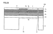
- FIG. 23 is a cross-sectional view taken along the line XXIII-XXIII in FIG.
- FIG. 1 A method for manufacturing a piezoelectric device according to the first embodiment of the present invention will be described with reference to FIGS. A flowchart of a method for manufacturing a piezoelectric device according to the present embodiment is shown in FIG.
- the method for manufacturing a piezoelectric device includes a substrate, a piezoelectric layer that is directly or indirectly supported by the substrate, disposed above the substrate, a heater, and a heater for driving the heater.
- a method of manufacturing a piezoelectric device comprising: an electrode; step S1 of forming the piezoelectric layer, the heater, and the heater electrode; driving the heater by energizing the heater electrode; And a step S2 of heat-treating the piezoelectric device with the generated heat.
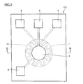
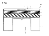
- FIGS. 3 An example of a piezoelectric device manufactured by the method for manufacturing a piezoelectric device in the present embodiment is shown in FIGS. 3 is a cross-sectional view taken along the line III-III in FIG.
- FIG. 2 shows the protective film 7 removed. Even in the state where the protective film 7 is present, each pad portion 8 has an opening in the protective film 7 and can be electrically connected to the pad portion 8 even from the upper side of the protective film 7. It has become.
- the piezoelectric device 101 is used as, for example, a pMUT. In the method for manufacturing a piezoelectric device in the present embodiment, the following steps are performed to manufacture the piezoelectric device 101.
- an AlN film as a support layer 5 is formed on a silicon substrate as a substrate 4 by a sputtering method so as to have a thickness of 500 nm or more and 3000 nm or less.
- a molybdenum film is formed to have a thickness of 100 nm to 200 nm so as to cover the upper surface of the support layer 5, and this molybdenum film is patterned.
- the heater 1 and the lower electrode 3 for driving reception are formed.
- the heater 1 is formed in a meander shape so as to surround the lower electrode 3 for driving reception.
- an AlN film for forming the piezoelectric layer 6 is formed by sputtering so as to have a thickness of 500 nm or more and 3000 nm or less, and is patterned as necessary. Subsequently, as shown in FIG. 7, a molybdenum film is formed and patterned. As a result, the driving / receiving upper electrode 2 is formed. Subsequently, an AlN film for forming the protective film 7 is formed so as to have a thickness of 100 nm to 1000 nm. Thus, a structure as shown in FIG. 8 is obtained.
- the film is formed because of the temperature distribution in the substrate 4 and the sputtering plasma density in the substrate surface.
- the stress that the film has has a distribution in the plane. This distribution generally has a difference of 100 MPa or more in the plane.
- an element that vibrates out of plane such as pMUT, has a resonance frequency due to the membrane being compressed or pulled under the influence of the stress. Variation occurs. For example, even if the resonance frequency is designed to be 300 kHz, the resonance frequency varies within a plane from, for example, 250 kHz to 500 kHz.
- the protective film 7 and the piezoelectric film 6 are etched in order to expose the electrode of the portion that becomes the pad portion 8.
- an aluminum film is formed so as to cover the electrode.
- the substrate 4 is etched from the back surface of the substrate 4 until the support layer 5 is reached. In this way, the structure shown in FIGS. 2 and 3 is obtained. A through hole 18 is formed in the substrate 4, and a portion remaining above the through hole 18 becomes a membrane portion 17.
- this piezoelectric device has a large stress variation in each deposited layer, resulting in a large frequency variation.
- the heater 1 is energized using the pad portion 8 connected to the heater 1.
- the meander heater 1 generates heat.
- Heat treatment is performed on the membrane portion 17 by this heat generation.
- This heat treatment is also referred to as “annealing”. Since the heater 1 has a very small heat capacity, it can be rapidly heated to 500 ° C. to 900 ° C. or 900 ° C. or higher in a very short time of less than 1 second when energized for about 100 mW to 1000 mW.
- the target temperature is higher than the film formation temperature at the time of sputtering for film formation, preferably 900 ° C. or higher.
- heat treatment is performed on the membrane portion 17 by energizing the heater 1 to generate heat.
- the crystallinity of the AlN film or Mo film is increased. Is improved.
- Ar gas trapped as impurities in the film is released from the film, and Al and Mo atoms located between the lattices are rearranged at appropriate positions.
- the thermal stress with the substrate 4 is not so much, and as a result, a pMUT with greatly improved initial frequency variation can be produced. .
- the heat capacity is small, and heat treatment can be performed in an extremely short time.
- the resonance frequency can be adjusted by heat treatment in the final product form or a state close thereto.
- Heat treatment can be performed at a desired location without any problem.
- heat treatment can be performed on a desired portion to a desired degree, and thus frequency variation can be reduced.
- an electrode for drive reception and an electrode for a heater that is, a heater electrode.
- the receiving function and the heater function can be used independently by separate electrodes.
- the heater 1 and the drive receiving electrode as the pMUT are arranged at different positions and do not interfere with each other.
- the membrane part 17 can be heated to 900 ° C. or higher.
- the linear expansion coefficients of AlN and Mo are close to each other, the melting points of AlN and Mo are extremely high, and for the AlN film, the Curie temperature is 1000 ° C. or higher and extremely high. Therefore, the piezoelectric performance is not impaired, and therefore the performance as a pMUT is not impaired.
- the film thickness ratio of the piezoelectric film and the support film as close as possible to 1: 1, it is possible to suppress deformation and breakage of the membrane portion 17 due to thermal stress.
- the piezoelectric layer 6 is not limited to an AlN film.
- the piezoelectric layer 6 may be formed of, for example, a ZnO film, or may be formed of a material obtained by doping an AlN film with Sc or the like.
- the heater 1 is disposed on the upper surface of the support layer 5
- the present invention is not limited to this configuration.
- the heater 1 may be disposed on the upper surface of the piezoelectric layer 6.
- the material of the support layer 5 and the protective film 7 is not limited to AlN, and may be another material having a linear expansion coefficient close to that of AlN.
- the material of the support layer 5 and the protective film 7 may be, for example, silicon or SiN.
- a plurality of piezoelectric devices are manufactured at the same time.
- the process proceeds simultaneously for a plurality of piezoelectric devices.
- variations in resonance frequency occur between a plurality of piezoelectric devices that are manufactured by processing in parallel, but in this embodiment, a plurality of piezoelectric devices are used at room temperature before heat treatment.
- the heater 1 can be energized at room temperature by repeating the cycle of resonance frequency measurement ⁇ heat treatment ⁇ resonance frequency measurement ⁇ heat treatment ⁇ . is there.
- the heater 1 can be energized at room temperature by repeating the cycle of resonance frequency measurement ⁇ heat treatment ⁇ resonance frequency measurement ⁇ heat treatment ⁇ . is there.
- the method for manufacturing a piezoelectric device includes a step of measuring a resonance frequency.
- the frequency is adjusted based on the measurement result of the step of measuring the resonance frequency. It is preferable to drive the heater. By doing so, since information on actual measurement results can be used, the heater can be driven under more accurate conditions.
- the method for manufacturing a piezoelectric device in the present embodiment preferably includes a step of measuring the resonance frequency again after the step of heat-treating the piezoelectric device.
- the resonance frequency of the piezoelectric device can be adjusted to a desired frequency.
- the step of adjusting the resonance frequency by heating with the heater may be performed after the substrate etching step and before the dicing step, as shown in FIG. As described above, it may be performed after finishing the packaging process.
- Thin film formation and patterning in FIGS. 9 and 10 means that the structure above the substrate 4 is formed by repeating film formation and patterning.
- Substrate etching means a process of forming the through hole 18 by etching the substrate 4 from the back surface, thereby forming the membrane portion 17.
- Diing means a process of cutting a plurality of piezoelectric devices on a single large substrate into individual piezoelectric devices.
- the material of the piezoelectric layer 6 is a perovskite type such as KNN (sodium potassium niobate: (K, Na) NbO 3 ) or PZT (lead zirconate titanate: Pb (Zr, Ti) O 3 ).
- the ferroelectric material is used.
- an SOI (Silicon on Insulator) substrate is used as the substrate 4 and the support layer 5.
- This SOI substrate has a structure in which a silicon layer, an oxide film, and an active layer are sequentially stacked from the bottom.
- the active layer is made of silicon.
- the active layer of this SOI substrate is used as the support layer 5.
- the thickness of the active layer of Si is 2 ⁇ m or more and 10 ⁇ m or less.
- a lower electrode made of a Pt / Ti laminated film is formed to a thickness of about 100 nm and patterned to form the heater 1 and the drive / reception lower electrode 3.
- a PZT film is formed by sputtering at a substrate temperature of about 600 ° C. to a thickness of 1000 nm to 3000 nm.
- An upper electrode made of Pt / Ti is formed thereon. Since Pt is resistant to oxidation, no protective film is required.
- the piezoelectric device according to the present embodiment does not include the protective film 7.
- the Pt film and the PZT film included in the upper electrode are formed by sputtering, the stress distribution is large in the plane of the SOI substrate for the same reason as AlN. Further, even when the PZT film is formed by using another method such as the Sol-Gel method, the stress distribution is obtained because the firing temperature distribution exists in the plane of the SOI substrate.
- an active layer of Si is used as a support layer is shown, but a layer made of PZT may be used as an active layer instead of Si.
- the silicon layer of the SOI substrate is etched from the back surface until it reaches the oxide film. Thereafter, the oxide film is removed if necessary.
- heat treatment is performed by energizing the heater 1 made of a Pt / Ti laminated film.
- the heat treatment is preferably performed at a temperature of 700 ° C. or higher and 1000 ° C. or lower, which is a temperature higher than the film forming temperature.
- a polarization treatment is required when used as a pMUT. Therefore, an appropriate voltage is applied between the electrodes formed on the upper and lower surfaces of the piezoelectric layer 6 for driving reception, and a polarization process is performed to align the polarization direction of the thick-electric layer 6.
- the same effect as in the first embodiment can be obtained.
- a piezoelectric device having good piezoelectric characteristics can be obtained.
- a distance sensor is configured by a combination of the transmission side piezoelectric device 41 and the reception side piezoelectric device 42.
- the transmission-side piezoelectric device 41 and the reception-side piezoelectric device 42 are each a piezoelectric device obtained by a manufacturing method as described in the previous embodiments.
- the receiving side piezoelectric device 42 can be displaced as indicated by an arrow 91.
- the ultrasonic wave 45 is transmitted from the transmission-side piezoelectric device 41 and received by the reception-side piezoelectric device 42, whereby the distance L is measured.
- the heater 1 used in the heat treatment can be used for another purpose.
- it can be used for removing moisture.
- the heater 1 is used in order to keep the temperature of the piezoelectric device constant in consideration of the temperature characteristics of the piezoelectric device.
- This heater can also be used as a temperature sensor for measuring the temperature of the piezoelectric device itself.
- Embodiment 4 With reference to FIG. 12 and FIG. 13, the manufacturing method of the piezoelectric device in Embodiment 4 based on this invention is demonstrated. 13 is a cross-sectional view taken along the line XIII-XIII in FIG.
- FIG. 12 shows the protective film 7 removed. Even in the state where the protective film 7 is present, each pad portion 8 has an opening in the protective film 7 and can be electrically connected to the pad portion 8 even from the upper side of the protective film 7. It has become. The same applies to the fifth to seventh embodiments.
- the piezoelectric device 102 is manufactured.
- the driving / receiving upper electrode 2 and the driving / receiving lower electrode 3 are arranged so as to sandwich the piezoelectric layer 6 at the outer peripheral portion of the membrane portion 17.
- the heater 1 is disposed on the upper surface of the support layer 5 at the center of the membrane portion 17 so as to be surrounded by these electrodes.
- the heater 1 includes a meandering portion.
- the manufacturing method of the piezoelectric device in the embodiments described so far can be employed. That is, when the heater 1 is energized, the membrane portion 17 can be heat-treated, and the frequency variation can be reduced.
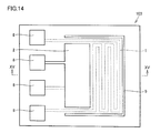
- Embodiment 5 With reference to FIG. 14 and FIG. 15, the manufacturing method of the piezoelectric device in Embodiment 5 based on this invention is demonstrated. 15 is a cross-sectional view taken along the line XV-XV in FIG.
- the piezoelectric device 103 is manufactured.
- the piezoelectric device 103 has a cantilever structure by providing slits 9 as shown in FIG.
- the drive / reception upper electrode 2 and the drive / reception lower electrode 3 are arranged so as to sandwich the piezoelectric layer 6 at the base side portion of the cantilever portion 19.
- the heater 1 is disposed on the upper surface of the support layer 5 at the tip side portion of the cantilever portion 19.
- the heater 1 includes a meandering portion.
- the cantilever portion since the cantilever portion is supported only by the base side portion, the stress in the cantilever portion is released, and the frequency variation is generally small. However, the cantilever portion may warp upward or downward, or the degree of deformation may vary within the cantilever portion.
- the piezoelectric device manufacturing method in the embodiments described so far can be employed. That is, by energizing the heater 1, the cantilever portion 19 can be heat-treated, and the degree of deformation can be reduced. By reducing the degree of deformation, frequency variations are reduced.
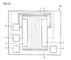
- Embodiment 6 With reference to FIG. 16, the manufacturing method of the piezoelectric device in Embodiment 6 based on this invention is demonstrated.
- the piezoelectric device 104 is manufactured.
- the piezoelectric device 104 has a double-supported beam structure by providing two slits 9 in parallel as shown in FIG.
- the drive / reception upper electrode 2 and the drive / reception lower electrode 3 are arranged so as to sandwich the piezoelectric layer 6 at the base side portion of the both-end supported beam portion, that is, the left end portion and the right end portion in FIG.
- a heater 1 is disposed on the upper surface of the support layer 5 at the center of the both-end supported beam portion.
- the heater 1 includes a meandering portion.
- the manufacturing method of the piezoelectric device in the embodiments described so far can be employed. That is, by energizing the heater 1, heat treatment of the both-end supported beam portion can be performed, and frequency variation can be reduced.
- Embodiment 7 With reference to FIG. 17, the manufacturing method of the piezoelectric device in Embodiment 7 based on this invention is demonstrated.
- the piezoelectric device 105 is manufactured.
- the piezoelectric device 105 includes a membrane portion similar to that shown in the first embodiment.
- the wiring formed in a meander shape on the upper surface of the support layer 5 in the membrane portion serves as the heater 1 and the lower electrode 3 for driving reception.
- the driving / receiving upper electrode 2 is disposed so as to overlap the heater 1 and the driving / receiving lower electrode 3.
- the piezoelectric layer 6 is sandwiched between the driving and receiving upper electrode 2 and the driving and receiving lower electrode 3.
- the manufacturing method of the piezoelectric device in the embodiments described so far can be employed. That is, when the heater 1 is energized, the membrane portion can be heat-treated, and the frequency variation can be reduced.
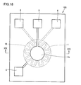
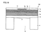
- Embodiment 8 With reference to FIG. 18 and FIG. 19, the manufacturing method of the piezoelectric device in Embodiment 8 based on this invention is demonstrated. 19 is a cross-sectional view taken along the line XIX-XIX in FIG.
- FIG. 18 shows the protective film 7 removed. Even in the state where the protective film 7 is present, each pad portion 8 has an opening in the protective film 7 and can be electrically connected to the pad portion 8 even from the upper side of the protective film 7. It has become. The same applies to the ninth and tenth embodiments.
- the piezoelectric device 106 is manufactured.
- the piezoelectric device 106 is similar to the piezoelectric device 101 shown in the first embodiment, but has a bimorph structure unlike the piezoelectric device 101. That is, in the piezoelectric device 106, the piezoelectric film has a two-layer structure, and the electrode has a three-layer structure so that a voltage can be individually applied to each of these piezoelectric films. As shown in a sectional view in FIG. 19, the piezoelectric device 106 includes a first piezoelectric film 6a and a second piezoelectric film 5a as two piezoelectric films.
- the piezoelectric device 106 includes, as three electrodes, a first electrode 2a for driving and receiving, a second electrode 3a for driving and receiving, and a third electrode 11 for driving and receiving. These three electrodes occupy almost the same region in plan view. These three electrodes are separated from each other in the thickness direction.
- the piezoelectric device 106 includes a lower protective film 10, a second piezoelectric film 5a, a first piezoelectric film 6a, and an upper protective film 7a in this order on the upper side of the substrate 4.
- a third electrode 11 for driving reception is disposed between the lower protective film 10 and the second piezoelectric film 5a.
- the third electrode 11 for driving and receiving is formed on the upper surface of the lower protective film 10.
- the second electrode 3a for driving reception and the heater 1 are disposed. These are formed on the upper surface of the second piezoelectric film 5a.
- the first electrode for driving reception 2a is disposed between the first piezoelectric film 6a and the upper protective film 7a.
- the first electrode 2a for driving and receiving is formed on the upper surface of the first piezoelectric film 6a.
- the manufacturing method of the piezoelectric device in the embodiments described so far can be adopted. That is, when the heater 1 is energized, the membrane portion 17 can be heat-treated, and frequency variations can be reduced.
- FIG. 21 is a cross-sectional view taken along the line XXI-XXI in FIG.
- the piezoelectric device 107 is manufactured.
- the piezoelectric device 107 is similar to the piezoelectric device 102 described in Embodiment 4, but has a bimorph structure unlike the piezoelectric device 102.
- the details of the bimorph structure are the same as those described in the eighth embodiment.
- the manufacturing method of the piezoelectric device in the embodiments described so far can be employed. That is, when the heater 1 is energized, the membrane portion 17 can be heat-treated, and the frequency variation can be reduced.
- Embodiment 10 With reference to FIG. 22 and FIG. 23, the manufacturing method of the piezoelectric device in Embodiment 10 based on this invention is demonstrated.
- 23 is a cross-sectional view taken along the line XXIII-XXIII in FIG.
- the piezoelectric device 108 is manufactured.
- the piezoelectric device 108 is similar to the piezoelectric device 103 described in Embodiment 5, but has a bimorph structure unlike the piezoelectric device 102.
- the details of the bimorph structure are the same as those described in the eighth embodiment.
- the manufacturing method of the piezoelectric device in the embodiments described so far can be employed. That is, when the heater 1 is energized, the cantilever portion 19 can be heat-treated, and the frequency variation can be reduced.
Landscapes
- Engineering & Computer Science (AREA)
- Manufacturing & Machinery (AREA)
- Physics & Mathematics (AREA)
- Acoustics & Sound (AREA)
- Chemical & Material Sciences (AREA)
- Crystallography & Structural Chemistry (AREA)
- Inorganic Chemistry (AREA)
- Piezo-Electric Or Mechanical Vibrators, Or Delay Or Filter Circuits (AREA)
- General Electrical Machinery Utilizing Piezoelectricity, Electrostriction Or Magnetostriction (AREA)
- Transducers For Ultrasonic Waves (AREA)
Abstract
圧電デバイスの製造方法は、基板(4)と、基板(4)によって直接または間接的に支持され、基板(4)より上側に配置された圧電体層(6)と、ヒータ(1)と、ヒータ(1)を駆動するためのヒータ電極とを備える、圧電デバイス(101)の製造方法であって、圧電体層(6)とヒータ(1)と前記ヒータ電極とを形成する工程と、前記ヒータ電極に通電することによってヒータ(1)を駆動し、ヒータ(1)から発する熱によって、圧電デバイス(101)の熱処理を行なう工程とを含む。
Description
本発明は、圧電デバイスの製造方法に関するものである。
従来より、"CMOS-Compatible AlN Piezoelectric Micromachined Ultrasonic Transducers", Stefon Shelton et al., 2009 IEEE International Ultrasonics Symposium Proceedings, pp. 402-405(非特許文献1)などに開示されているように、基板と、基板の上方に設けられた圧電体層および電極とを備える、圧電デバイスが知られている。このような圧電デバイスは、フィルタ、アクチュエータ、センサ、pMUT(piezoelectric Micromachined Ultrasonic Transducers)などに用いられる。
このような圧電デバイスの一例として、米国特許出願公開US2010/0195851A1(特許文献1)の段落0017~0023、図1A、図1Bには、トランスデューサと、基板と、温度補償素子とを備えるMEMSデバイスが開示されている。トランスデューサは、たとえば屈曲振動する圧電超音波トランスデューサであり、基板の上方に配置されている。温度補償素子は、たとえばヒータ素子であり、トランスデューサの周囲かつ下面側であって、基板上に配置されている。
また、米国特許出願公開US2010/0134209A1(特許文献2)の段落0070~0076、図2Aおよび図2Bには、センサ素子と、半導体基板と、ヒータ素子とを備えるセンサ・アレイが開示されている。センサ素子は、圧電体層と2つの電極とを有する圧電共振素子であり、基板上に配置されている。ヒータ素子は、センサ素子の周囲かつ基板上に配置されている。
これらの文献に記載されているヒータ素子は、発振周波数を安定化するための圧電デバイスの温度調整、圧電デバイスの表面に付着した水分の除去などに用いられる。
これらの圧電デバイスには、製造時に生じる共振周波数のばらつき(以下「周波数ばらつき」ともいう。)が大きいという問題がある。周波数ばらつきを決める要因としては、それぞれの厚み、長さなどの寸法などいくつかある。特に、最も重要な要因は、メンブレン部を構成する部材の応力である。メンブレン部を構成する部材とは、圧電体層、電極などである。
メンブレン部を構成する部材の応力は、スパッタリング法やゾルゲル法などの製造方法によって変化しうる。AlNからなる圧電体層はスパッタリング法によって形成されることが多い。AlNからなる圧電体層をスパッタリング法で形成する場合、基板の温度分布や、プラズマの分布によって、圧電体層の応力がウェハ面内で大きくばらつくことがある。この結果、圧電デバイスの周波数ばらつきが大きくなる。
特開2001-85752号公報(特許文献3)には、半導体センサにおいて、機能膜の応力を緩和するために、熱処理炉を用いて熱処理を行なうことが開示されている。しかし、熱処理炉を用いた熱処理は、熱処理炉を所望の温度まで昇温させた上で圧電デバイス全体を加熱するため、時間とコストがかかるという欠点がある。
特開平10-256570号公報(特許文献4)には、薄膜デバイスにおいて、優れた特性の薄膜を形成するために、基板の上に形成されたヒータ素子としての局部加熱部で基板を加熱した状態で圧電体材料からなる薄膜を形成することが開示されている。しかし、AlNからなる圧電体層の応力の大きさには、スパッタリング法における基板の温度分布やプラズマの分布が影響するため、この方法を用いても製造時に生じる周波数ばらつきが大きいという問題が解決されるとは限らない。
"CMOS-Compatible AlN Piezoelectric Micromachined Ultrasonic Transducers", Stefon Shelton et al., 2009 IEEE International Ultrasonics Symposium Proceedings, pp. 402-405
そこで、本発明は、周波数ばらつきを低減することができる圧電デバイスの製造方法を提供することを目的とする。
上記目的を達成するため、本発明に基づく圧電デバイスの製造方法は、基板と、上記基板によって直接または間接的に支持され、上記基板より上側に配置された圧電体層と、ヒータと、上記ヒータを駆動するためのヒータ電極とを備える、圧電デバイスの製造方法であって、上記圧電体層と上記ヒータと上記ヒータ電極とを形成する工程と、上記ヒータ電極に通電することによって上記ヒータを駆動し、上記ヒータから発する熱によって、上記圧電デバイスの熱処理を行なう工程とを含む。
上記発明において好ましくは、共振周波数を測定する工程を含み、上記圧電デバイスの熱処理を行なう工程では、上記共振周波数を測定する工程の測定結果を踏まえて周波数を調整して上記ヒータを駆動する。
上記発明において好ましくは、上記圧電デバイスの熱処理を行なう工程の後で、再度共振周波数を測定する工程を含む。
上記発明において好ましくは、上記圧電体層は、少なくとも一部が上記基板に重ならないメンブレン部となっており、少なくとも上記メンブレン部において上記圧電体層の下側に配置された下部電極と、上記メンブレン部において上記圧電体層を挟んで上記下部電極の少なくとも一部に対向するように上記圧電体層の上側に配置された上部電極とを備え、上記ヒータは上記メンブレン部に配置されている。
上記発明において好ましくは、上記上部電極および上記圧電体層を覆うように保護膜が設けられている。
上記発明において好ましくは、上記基板は貫通孔または凹部を有し、上記貫通孔または凹部を覆うように支持層を備え、上記圧電体層は上記支持層を介する形で上記基板によって支持されている。
上記発明において好ましくは、上記圧電体層は、AlN、KNNおよびPZTからなる群から選択されたいずれかを主材料とする。
上記発明において好ましくは、上記保護膜はAlNを主材料とする。
上記発明において好ましくは、上記支持層はAlNを主材料とする。
上記発明において好ましくは、上記支持層はAlNを主材料とする。
上記発明において好ましくは、上記ヒータ電極は、WまたはMoを主材料とする。
本発明によれば、圧電デバイス内に形成されたヒータを用いて圧電デバイスの熱処理を行なうので、熱容量が小さく、極めて短時間で熱処理をすることができる。この熱処理によって所望の箇所に所望の程度だけ共振周波数を調整することができるので、周波数ばらつきを低減することができる。
(実施の形態1)
図1~図8を参照して、本発明に基づく実施の形態1における圧電デバイスの製造方法について説明する。本実施の形態における圧電デバイスの製造方法のフローチャートを図1に示す。
図1~図8を参照して、本発明に基づく実施の形態1における圧電デバイスの製造方法について説明する。本実施の形態における圧電デバイスの製造方法のフローチャートを図1に示す。
本実施の形態における圧電デバイスの製造方法は、基板と、前記基板によって直接または間接的に支持され、前記基板より上側に配置された圧電体層と、ヒータと、前記ヒータを駆動するためのヒータ電極とを備える、圧電デバイスの製造方法であって、前記圧電体層と前記ヒータと前記ヒータ電極とを形成する工程S1と、前記ヒータ電極に通電することによって前記ヒータを駆動し、前記ヒータから発する熱によって、前記圧電デバイスの熱処理を行なう工程S2とを含む。
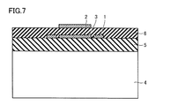
本実施の形態における圧電デバイスの製造方法によって製造される圧電デバイスの一例を図2および図3に示す。図3は図2におけるIII-III線に関する矢視断面図である。説明の便宜のため、図2では保護膜7を取り去った状態で示している。保護膜7がある状態であっても、各パッド部8においては保護膜7に開口部が設けられており、保護膜7の上側からでもパッド部8に対して電気的に接続可能な構成となっている。この圧電デバイス101は、たとえばpMUTとして用いられるものである。本実施の形態における圧電デバイスの製造方法では、圧電デバイス101を製造するために以下の各工程を行なう。
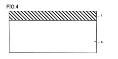
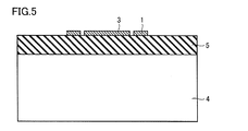
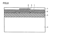
まず、図4に示すように、基板4としてのシリコン基板に、支持層5としてのAlN膜を厚み500nm以上3000nm以下となるようにスパッタ法を用いて成膜する。続いて、支持層5の上面を覆うようにモリブデン膜を厚み100nm以上200nm以下となるように成膜し、このモリブデン膜をパターニングする。これによって、図5に示すように、ヒータ1および駆動受信用下部電極3が形成される。ヒータ1は駆動受信用下部電極3を取り囲むようにミアンダ状に形成される。続いて、図6に示すように、圧電体層6とするためのAlN膜を厚み500nm以上3000nm以下となるようにスパッタ法を用いて成膜し、必要に応じてパターニングする。続いて、図7に示すように、モリブデン膜を成膜し、パターニングする。これによって、駆動受信用上部電極2が形成される。続いて、保護膜7とするためのAlN膜を厚み100nm以上1000nm以下となるように形成する。こうして、図8に示したような構造が得られる。
ここまでに示したようなAlN膜や電極としてのモリブデン膜を形成する際には、基板4に温度分布が存在することや、スパッタのプラズマ密度が基板表面に分布をもつことから、成膜される膜が有する応力は面内で分布をもつことになる。この分布は面内で100MPa以上の違いとなるのが一般的である。成膜された膜が100MPaの応力をもつとしたとき、pMUTのように、面外振動をするような素子は、応力の影響でメンブレンが圧縮されたり、引っ張られたりすることで、共振周波数にばらつきが生じる。たとえば、共振周波数が300kHzとなるように設計したとしても、面内でたとえば250kHzから500kHzまでばらつくことになる。
続いて、パッド部8となる部分の電極を露出させるために保護膜7および圧電膜6をエッチングする。パッド部8として電極が露出した部分(図示せず)においては電極を覆うようにアルミニウム膜を形成する。
続いて、基板4の裏面から、支持層5に到達するまで基板4をエッチングする。このようにして、図2および図3に示した構造が得られる。基板4に貫通孔18が形成され、この貫通孔18の上側に残る部分はメンブレン部17となる。
ただし、上述のように、ここまでの時点では、この圧電デバイスは成膜された各層に大きな応力ばらつきをもっており、結果として大きな周波数ばらつきをもつことになる。
続いて、ヒータ1に接続されているパッド部8を利用してヒータ1に通電する。これによりミアンダ状のヒータ1が発熱する。この発熱によってメンブレン部17に対する熱処理を行なう。この熱処理のことは「アニール処理」ともいう。ヒータ1は熱容量が極めて小さいので、100mW~1000mW程度通電すると1秒未満の極めて短時間に急速に500℃~900℃または900℃以上にまで加熱することが可能である。ここで目標とする温度は成膜のスパッタ時の成膜温度以上、好ましくは900℃以上に加熱する。このような熱処理を終えることによって、圧電デバイス101が得られる。
本実施の形態では、ヒータ1に通電して発熱させることによってメンブレン部17に対する熱処理を行なうこととしているが、メンブレン部17を成膜温度以上に加熱することで、AlN膜やMo膜の結晶性が改善される。具体的には、膜中に不純物してとりこまれたArガスが膜中から放出されることや、格子間に位置していたAlやMoの原子が適切な位置に再配置される。また熱処理後に冷却される過程でも、既にメンブレン形状であるため、基板4との間での熱応力はさほどかからず、結果として、初期の周波数ばらつきが大きく改善されたpMUTを作製することができる。
本実施の形態では、メンブレン部17に形成したヒータ1を用いて加熱するので、熱容量が小さく、極めて短時間で熱処理をすることができる。また、本実施の形態では、最終の商品形態またはそれに近い状態で、熱処理により共振周波数を調整することができる。本実施の形態では、局所的に加熱することが可能であるので、パッド部8のアルミニウム合金や、ダイボンドに用いられた接着剤などのように耐熱性が低い材料が周辺に存在していても問題なく所望の箇所に熱処理を行なうことができる。
本実施の形態における圧電デバイスの製造方法によれば、上述のように所望の箇所に所望の程度だけ熱処理を施すことができるので、周波数ばらつきを低減することができる。
本実施の形態で示したように、駆動受信用の電極と、ヒータのための電極すなわちヒータ電極とを別々に設けておくことが可能であり、そのように構成した場合、pMUTとしての駆動および受信の機能とヒータの機能とを独立に別々の電極によって使用することができる。
メンブレン部17において、ヒータ1と、pMUTとしての駆動受信用の電極とは、別々の位置に配置されており、相互に干渉しない。
1つの圧電デバイスで送信と受信とを兼ねて行なう場合もあるが、送信用と受信用とで別々の圧電デバイスを用意し、送信用と受信用とからなる1つのペアの圧電デバイスとする場合、このペア間での感度ばらつきが問題となるが、本実施の形態では、熱処理を行なうことによって共振周波数のばらつきは小さくなるので、ペア間での感度ばらつきについても小さくすることが可能である。
本実施の形態では、メンブレン部17は900℃以上に加熱することが可能である。
なお、900℃以上に加熱する際は、AlN膜の酸化を防ぐために、N2雰囲気中で行なうことが好ましい。また、900℃以上に加熱する際もAlNとMoとの線膨張係数が互いに近いこと、AlNおよびMoの融点が極めて高いこと、AlN膜に関しては、キュリー温度が1000℃以上であって極めて高いことから、圧電性能が損なわれることはなく、したがって、pMUTとしての性能が損なわれることはない。また、圧電膜と支持膜との膜厚比をなるべく1:1に近づけることで、熱応力によるメンブレン部17の変形や破壊を抑えることが可能である。
なお、900℃以上に加熱する際は、AlN膜の酸化を防ぐために、N2雰囲気中で行なうことが好ましい。また、900℃以上に加熱する際もAlNとMoとの線膨張係数が互いに近いこと、AlNおよびMoの融点が極めて高いこと、AlN膜に関しては、キュリー温度が1000℃以上であって極めて高いことから、圧電性能が損なわれることはなく、したがって、pMUTとしての性能が損なわれることはない。また、圧電膜と支持膜との膜厚比をなるべく1:1に近づけることで、熱応力によるメンブレン部17の変形や破壊を抑えることが可能である。
なお、本実施の形態では圧電体層6としてAlN膜を用いる例を示したが、圧電体層6はAlN膜に限らない。圧電体層6は、たとえばZnO膜で形成してもよく、あるいは、AlN膜にScなどをドープした材料で形成してもよい。
本実施の形態では、ヒータ1を支持層5の上面に配置する例を示したが、この構成に限らない。ヒータ1を圧電体層6の上面に配置してもよい。
支持層5、保護膜7の材料は、AlNに限定されず、線膨張係数がAlNと近い他の材料であってもよい。支持層5、保護膜7の材料は、たとえば、シリコンやSiNであってもよい。
通常、同時に複数の圧電デバイスが製造される。この場合、複数の圧電デバイスに対して同時並行的に工程が進行する。従来であれば同時並行的に処理されて製造される複数の圧電デバイスの相互間でも共振周波数のばらつきが生じると考えられるが、本実施の形態では、熱処理を行なう前に室温で複数の圧電デバイスの共振周波数を個別に測定しておき、それぞれの圧電デバイスの共振周波数と目標とする共振周波数との差に応じた熱処理(温度や時間)をそれぞれの圧電デバイスに対して個別に行なうことによって、同時に製造される複数の圧電デバイス間の周波数ばらつきを抑えることができる。
ヒータ1への通電は、個別の圧電デバイスにおいて所望の周波数を得るために、室温で、共振周波数測定→熱処理→共振周波数測定→熱処理→…のサイクルを繰り返して、周波数ばらつきを抑えることも可能である。このような方法を採用することによって、さらに周波数ばらつきが小さい複数の圧電デバイスを短時間で形成することが可能である。
すなわち、本実施の形態における圧電デバイスの製造方法は、共振周波数を測定する工程を含み、前記圧電デバイスの熱処理を行なう工程では、前記共振周波数を測定する工程の測定結果を踏まえて周波数を調整して前記ヒータを駆動することが好ましい。このようにすることで、実際の測定結果の情報を利用することができるので、より的確な条件でヒータの駆動を行なうことができる。
本実施の形態における圧電デバイスの製造方法は、前記圧電デバイスの熱処理を行なう工程の後で、再度共振周波数を測定する工程を含むことが好ましい。このようにすることで、熱処理によって変化した後の共振周波数を把握することができるので、共振周波数が所望の値になったか否かを確認することができる。また、さらに熱処理を繰り返す場合には、前回の熱処理後の共振周波数の値の情報を利用して、より的確な条件でヒータの駆動を行なうことができる。
本実施の形態では、このように熱処理を行なう工程と共振周波数を測定する工程とを繰り返すことができるので、圧電デバイスの共振周波数を所望の周波数に調整することが可能である。
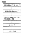
なお、このようにヒータで加熱することによって共振周波数を調整する工程は、図9に示すように、基板エッチングの工程より後でダイシングの工程より前に行なうこととしてもよいが、図10に示すように、パッケージングの工程まで終えた後で行なうこととしてもよい。図9および図10でいう「薄膜形成およびパターニング」とは基板4より上側の構造を、成膜およびパターニングの繰り返しによって行なうことを意味する。「基板エッチング」とは、基板4に対して裏面からエッチングすることによって貫通孔18を形成し、これによって、メンブレン部17を形成する工程を意味する。「ダイシング」とは、1枚の大きな基板上で複数の圧電デバイスを作製している場合に、個別の圧電デバイスに切り分ける工程を意味する。
(実施の形態2)
図2および図3を再び参照し、本発明に基づく実施の形態2における圧電デバイスの製造方法について説明する。本実施の形態では、圧電デバイスの構造自体は実施の形態1で説明したものと同様であるが、主に材料が異なる。文中の符号は、図2および図3におけるものを用いる。
図2および図3を再び参照し、本発明に基づく実施の形態2における圧電デバイスの製造方法について説明する。本実施の形態では、圧電デバイスの構造自体は実施の形態1で説明したものと同様であるが、主に材料が異なる。文中の符号は、図2および図3におけるものを用いる。
本実施の形態では、圧電体層6の材料として、KNN(ニオブ酸ナトリウムカリウム:(K,Na)NbO3)やPZT(チタン酸ジルコン酸鉛:Pb(Zr,Ti)O3)などペロブスカイト型の強誘電体を用いる。本実施の形態では、基板4および支持層5をなすものとしてSOI(Silicon on Insulator)基板を用いる。このSOI基板は、下から順に、シリコン層、酸化膜、活性層の順に積層された構造となっている。活性層はシリコンからなる。
本実施の形態では、このSOI基板の活性層を支持層5として使用する。Siの活性層の厚みは2μm以上10μm以下である。このSOI基板上にPt/Tiの積層膜からなる下部電極を100nm程度成膜し、パターニングし、ヒータ1および駆動受信用下部電極3を形成する。この上に基板温度600℃程度で、PZT膜をスパッタリングで1000nm~3000nm形成する。その上にPt/Tiからなる上部電極を形成する。Ptは酸化に強いので、保護膜は特に必要としない。図3に示した圧電デバイス101は保護膜7を備えていたが、本実施の形態における圧電デバイスには保護膜7は備わっていない。上部電極に含まれるPt膜およびPZT膜をスパッタ法で成膜した場合、AlNと同様の理由で、SOI基板の面内で大きな応力分布をもつことになる。また、たとえ、Sol-Gel法のような他の手法を用いてPZT膜を成膜した場合にも、SOI基板の面内で焼成温度分布が存在することから応力分布を持つことになる。なお、本実施の形態ではSiの活性層を支持層として用いる例を示したが、Siに代えてPZTからなる層を活性層として用いてもよい。
続いて、裏面からSOI基板のシリコン層を、酸化膜に到達するまで、エッチングする。この後に必要に応じて酸化膜は除去する。
この後、Pt/Tiの積層膜からなるヒータ1に通電することで、熱処理を行なう。この場合、熱処理は、成膜温度以上の温度である700℃以上1000℃以下程度で行なうことが好ましい。なお、熱処理温度がキュリー温度を超えるので、pMUTとして使用する際には分極処理が必要である。そこで、圧電体層6の上下面に駆動受信用として形成した電極間に適切な電圧を加えて、厚電体層6の分極の向きを揃える分極処理を行なう。
本実施の形態においても実施の形態1と同様の効果を得ることができる。本実施の形態では、AlNよりも圧電性が高い材料を用いているので、良好な圧電特性を有する圧電デバイスを得ることができる。
(実施の形態3)
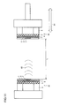
実施の形態1,2では圧電デバイスをpMUTとして用いる例を示したが、pMUTにおいて、実際の使用時に、結露により水分が付着し、この水分が超音波の励振あるいは受信に影響を与える場合がある。この場合、周波数ばらつきを減らすために使用したヒータを使って、メンブレンを100度以上に加熱することで水分を除去することが可能である。あるいはこのヒータ電極の抵抗値を測定することで、温度センサとしても使用可能である。具体的には、図11に示すように例えば距離センサとして用いる場合、表面に付着した水分を蒸発させたりするために、このヒータを使用することが可能である。図11においては、送信側圧電デバイス41と受信側圧電デバイス42との組合せによって距離センサが構成されている。送信側圧電デバイス41と受信側圧電デバイス42とは、それぞれこれまでの実施の形態で説明したような製造方法で得られた圧電デバイスである。受信側圧電デバイス42は矢印91に示すように変位しうる。送信側圧電デバイス41から超音波45が送出され、受信側圧電デバイス42によって受信されることにより、距離Lを測定する。
実施の形態1,2では圧電デバイスをpMUTとして用いる例を示したが、pMUTにおいて、実際の使用時に、結露により水分が付着し、この水分が超音波の励振あるいは受信に影響を与える場合がある。この場合、周波数ばらつきを減らすために使用したヒータを使って、メンブレンを100度以上に加熱することで水分を除去することが可能である。あるいはこのヒータ電極の抵抗値を測定することで、温度センサとしても使用可能である。具体的には、図11に示すように例えば距離センサとして用いる場合、表面に付着した水分を蒸発させたりするために、このヒータを使用することが可能である。図11においては、送信側圧電デバイス41と受信側圧電デバイス42との組合せによって距離センサが構成されている。送信側圧電デバイス41と受信側圧電デバイス42とは、それぞれこれまでの実施の形態で説明したような製造方法で得られた圧電デバイスである。受信側圧電デバイス42は矢印91に示すように変位しうる。送信側圧電デバイス41から超音波45が送出され、受信側圧電デバイス42によって受信されることにより、距離Lを測定する。
本実施の形態では、熱処理の際に用いたヒータ1を別用途に使用することができる。たとえば水分を飛ばすことに用いることができる。あるいは、圧電デバイスの温度特性を考慮して圧電デバイスの温度を一定に保つために、ヒータ1が用いられる。このヒータを圧電デバイス自体の温度を測定するための温度センサとして使用することもできる。
(pMUT以外の用途)
ここまでの実施の形態では、圧電デバイスがpMUTとして用いられる場合を前提に説明してきたが、圧電デバイスの用途はpMUTに限らない。RFフィルタ、MEMS発振子として圧電デバイスが用いられる場合においてもこのような共振周波数調整の技術を用いることができる。
ここまでの実施の形態では、圧電デバイスがpMUTとして用いられる場合を前提に説明してきたが、圧電デバイスの用途はpMUTに限らない。RFフィルタ、MEMS発振子として圧電デバイスが用いられる場合においてもこのような共振周波数調整の技術を用いることができる。
(pMUTの構造の変形例)
ここまでの実施の形態では、メンブレン部17のうち外周部にヒータ1を配置した構成のpMUTを示したが、pMUTとしての圧電デバイスには他の構成も考えられる。以下に、実施の形態4~7として説明する。
ここまでの実施の形態では、メンブレン部17のうち外周部にヒータ1を配置した構成のpMUTを示したが、pMUTとしての圧電デバイスには他の構成も考えられる。以下に、実施の形態4~7として説明する。
(実施の形態4)
図12、図13を参照して、本発明に基づく実施の形態4における圧電デバイスの製造方法について説明する。図13は、図12におけるXIII-XIII線に関する矢視断面図である。
図12、図13を参照して、本発明に基づく実施の形態4における圧電デバイスの製造方法について説明する。図13は、図12におけるXIII-XIII線に関する矢視断面図である。
説明の便宜のため、図12では保護膜7を取り去った状態で示している。保護膜7がある状態であっても、各パッド部8においては保護膜7に開口部が設けられており、保護膜7の上側からでもパッド部8に対して電気的に接続可能な構成となっている。このことは、実施の形態5~7においても同様である。
本実施の形態では圧電デバイス102を製造する。圧電デバイス102では、図13に示すように、メンブレン部17の外周部において圧電体層6を挟むように駆動受信用上部電極2および駆動受信用下部電極3が配置されている。これらの電極に取り囲まれるようにして、メンブレン部17の中央部において支持層5の上面にヒータ1が配置されている。ヒータ1はミアンダ状の部分を含んでいる。
このような構成のpMUTとしての圧電デバイスを製造する際にも、これまでに説明した実施の形態における圧電デバイスの製造方法を採用することができる。すなわち、ヒータ1に通電することによって、メンブレン部17の熱処理を行なうことができ、周波数ばらつきを低減することができる。
(実施の形態5)
図14、図15を参照して、本発明に基づく実施の形態5における圧電デバイスの製造方法について説明する。図15は、図14におけるXV-XV線に関する矢視断面図である。
図14、図15を参照して、本発明に基づく実施の形態5における圧電デバイスの製造方法について説明する。図15は、図14におけるXV-XV線に関する矢視断面図である。
本実施の形態では圧電デバイス103を製造する。圧電デバイス103では、図14に示すようにスリット9が設けられることによって、片持ち梁構造となっている。片持ち梁部19の根元側部分において圧電体層6を挟むように駆動受信用上部電極2および駆動受信用下部電極3が配置されている。片持ち梁部19の先端側部分において支持層5の上面にヒータ1が配置されている。ヒータ1はミアンダ状の部分を含んでいる。片持ち梁構造の圧電デバイスにおいては、片持ち梁部は根元側部分のみで支持されているので、片持ち梁部内の応力は解放されており、一般的に周波数ばらつきは小さい。しかしながら、片持ち梁部が上方向または下方向に反ったり、片持ち梁部内で変形の度合いが異なったりすることがある。
本実施の形態で説明したような構成のpMUTとしての圧電デバイスを製造する際にも、これまでに説明した実施の形態における圧電デバイスの製造方法を採用することができる。すなわち、ヒータ1に通電することによって、片持ち梁部19の熱処理を行なうことができ、変形の度合いを低減することができる。変形の度合いが低減されることによって、周波数ばらつきが低減される。
(実施の形態6)
図16を参照して、本発明に基づく実施の形態6における圧電デバイスの製造方法について説明する。
図16を参照して、本発明に基づく実施の形態6における圧電デバイスの製造方法について説明する。
本実施の形態では圧電デバイス104を製造する。圧電デバイス104では、図16に示すように2本のスリット9が平行に設けられることによって、両持ち梁構造となっている。両持ち梁部の根元側部分すなわち図16における左端部および右端部において圧電体層6を挟むように駆動受信用上部電極2および駆動受信用下部電極3が配置されている。両持ち梁部の中央部において支持層5の上面にヒータ1が配置されている。ヒータ1はミアンダ状の部分を含んでいる。
このような構成のpMUTとしての圧電デバイスを製造する際にも、これまでに説明した実施の形態における圧電デバイスの製造方法を採用することができる。すなわち、ヒータ1に通電することによって、両持ち梁部の熱処理を行なうことができ、周波数ばらつきを低減することができる。
(実施の形態7)
図17を参照して、本発明に基づく実施の形態7における圧電デバイスの製造方法について説明する。
図17を参照して、本発明に基づく実施の形態7における圧電デバイスの製造方法について説明する。
本実施の形態では圧電デバイス105を製造する。圧電デバイス105では、実施の形態1で示したのと同様のメンブレン部を備えている。圧電デバイス105では、図17に示すように、メンブレン部において支持層5の上面にミアンダ状に形成された配線がヒータ1と駆動受信用下部電極3とを兼ねている。ヒータ1兼駆動受信用下部電極3と重なるように駆動受信用上部電極2が配置されている。圧電体層6は、駆動受信用上部電極2と駆動受信用下部電極3とによって挟まれている。
このような構成のpMUTとしての圧電デバイスを製造する際にも、これまでに説明した実施の形態における圧電デバイスの製造方法を採用することができる。すなわち、ヒータ1に通電することによって、メンブレン部の熱処理を行なうことができ、周波数ばらつきを低減することができる。
(実施の形態8)
図18および図19を参照して、本発明に基づく実施の形態8における圧電デバイスの製造方法について説明する。図19は、図18におけるXIX-XIX線に関する矢視断面図である。
図18および図19を参照して、本発明に基づく実施の形態8における圧電デバイスの製造方法について説明する。図19は、図18におけるXIX-XIX線に関する矢視断面図である。
説明の便宜のため、図18では保護膜7を取り去った状態で示している。保護膜7がある状態であっても、各パッド部8においては保護膜7に開口部が設けられており、保護膜7の上側からでもパッド部8に対して電気的に接続可能な構成となっている。このことは、実施の形態9,10においても同様である。
本実施の形態では圧電デバイス106を製造する。圧電デバイス106は、実施の形態1で示した圧電デバイス101と似ているが、圧電デバイス101と異なり、バイモルフ構造となっている。すなわち、圧電デバイス106においては、圧電膜が2層構造となっており、これらの圧電膜の各々に個別に電圧を印加できるように電極が3層構造となっている。図19に断面図で示すように、圧電デバイス106は、2つの圧電膜として第1圧電膜6aおよび第2圧電膜5aを備える。圧電デバイス106は、3つの電極として、駆動受信用第1電極2aと、駆動受信用第2電極3aと、駆動受信用第3電極11とを備えている。これら3つの電極は平面的に見ればほぼ同じ領域を占めている。これら3つの電極は厚み方向に互いに離隔している。
圧電デバイス106は、基板4の上側に、下部保護膜10、第2圧電膜5a、第1圧電膜6a、上部保護膜7aをこの順に含んでいる。下部保護膜10と第2圧電膜5aとの間には駆動受信用第3電極11が配置されている。駆動受信用第3電極11は下部保護膜10の上面に形成されている。第2圧電膜5aと第1圧電膜6aとの間には駆動受信用第2電極3aおよびヒータ1が配置されている。これらは第2圧電膜5aの上面に形成されている。第1圧電膜6aと上部保護膜7aとの間には駆動受信用第1電極2aが配置されている。駆動受信用第1電極2aは第1圧電膜6aの上面に形成されている。
メンブレン部17として露出する部分の最下面は下部保護膜10によって覆われている。
このような構成のpMUTとしての圧電デバイス106を製造する際にも、これまでに説明した実施の形態における圧電デバイスの製造方法を採用することができる。すなわち、ヒータ1に通電することによって、メンブレン部17の熱処理を行なうことができ、周波数ばらつきを低減することができる。
(実施の形態9)
図20および図21を参照して、本発明に基づく実施の形態9における圧電デバイスの製造方法について説明する。図21は、図20におけるXXI-XXI線に関する矢視断面図である。
図20および図21を参照して、本発明に基づく実施の形態9における圧電デバイスの製造方法について説明する。図21は、図20におけるXXI-XXI線に関する矢視断面図である。
本実施の形態では圧電デバイス107を製造する。圧電デバイス107は、実施の形態4で示した圧電デバイス102と似ているが、圧電デバイス102と異なり、バイモルフ構造となっている。バイモルフ構造の詳細は、実施の形態8で説明したものと同様である。
このような構成のpMUTとしての圧電デバイス107を製造する際にも、これまでに説明した実施の形態における圧電デバイスの製造方法を採用することができる。すなわち、ヒータ1に通電することによって、メンブレン部17の熱処理を行なうことができ、周波数ばらつきを低減することができる。
(実施の形態10)
図22および図23を参照して、本発明に基づく実施の形態10における圧電デバイスの製造方法について説明する。図23は、図22におけるXXIII-XXIII線に関する矢視断面図である。
図22および図23を参照して、本発明に基づく実施の形態10における圧電デバイスの製造方法について説明する。図23は、図22におけるXXIII-XXIII線に関する矢視断面図である。
本実施の形態では圧電デバイス108を製造する。圧電デバイス108は、実施の形態5で示した圧電デバイス103と似ているが、圧電デバイス102と異なり、バイモルフ構造となっている。バイモルフ構造の詳細は、実施の形態8で説明したものと同様である。
このような構成のpMUTとしての圧電デバイス108を製造する際にも、これまでに説明した実施の形態における圧電デバイスの製造方法を採用することができる。すなわち、ヒータ1に通電することによって、片持ち梁部19の熱処理を行なうことができ、周波数ばらつきを低減することができる。
なお、上記実施の形態のうち複数を適宜組み合わせて採用してもよい。
なお、今回開示した上記実施の形態はすべての点で例示であって制限的なものではない。本発明の範囲は上記した説明ではなくて請求の範囲によって示され、請求の範囲と均等の意味および範囲内でのすべての変更を含むものである。
なお、今回開示した上記実施の形態はすべての点で例示であって制限的なものではない。本発明の範囲は上記した説明ではなくて請求の範囲によって示され、請求の範囲と均等の意味および範囲内でのすべての変更を含むものである。
1 ヒータ、2 駆動受信用上部電極、2a 駆動受信用第1電極、3 駆動受信用下部電極、3a 駆動受信用第2電極、4 基板、5 支持層、5a 第2圧電膜、6 圧電体層、6a 第1圧電膜、7 保護膜、7a 上部保護膜、8 パッド部、9 スリット、10 下部保護膜、11 駆動受信用第3電極、17 メンブレン部、18 貫通孔、19 片持ち梁部、41 送信側圧電デバイス、42 受信側圧電デバイス、45 超音波、91 矢印、101,102,103,104,105,106,107,108 圧電デバイス。
Claims (10)
- 基板と、前記基板によって直接または間接的に支持され、前記基板より上側に配置された圧電体層と、ヒータと、前記ヒータを駆動するためのヒータ電極とを備える、圧電デバイスの製造方法であって、
前記圧電体層と前記ヒータと前記ヒータ電極とを形成する工程と、
前記ヒータ電極に通電することによって前記ヒータを駆動し、前記ヒータから発する熱によって、前記圧電デバイスの熱処理を行なう工程とを含む、圧電デバイスの製造方法。 - 共振周波数を測定する工程を含み、
前記圧電デバイスの熱処理を行なう工程では、前記共振周波数を測定する工程の測定結果を踏まえて周波数を調整して前記ヒータを駆動する、請求項1に記載の圧電デバイスの製造方法。 - 前記圧電デバイスの熱処理を行なう工程の後で、再度共振周波数を測定する工程を含む、請求項2に記載の圧電デバイスの製造方法。
- 前記圧電体層は、少なくとも一部が前記基板に重ならないメンブレン部となっており、少なくとも前記メンブレン部において前記圧電体層の下側に配置された下部電極と、前記メンブレン部において前記圧電体層を挟んで前記下部電極の少なくとも一部に対向するように前記圧電体層の上側に配置された上部電極とを備え、前記ヒータは前記メンブレン部に配置されている、請求項1から3のいずれかに記載の圧電デバイスの製造方法。
- 前記上部電極および前記圧電体層を覆うように保護膜が設けられている、請求項4に記載の圧電デバイスの製造方法。
- 前記基板は貫通孔または凹部を有し、前記貫通孔または凹部を覆うように支持層を備え、前記圧電体層は前記支持層を介する形で前記基板によって支持されている、請求項1から5のいずれかに記載の圧電デバイスの製造方法。
- 前記圧電体層は、AlN、KNNおよびPZTからなる群から選択されたいずれかを主材料とする、請求項1から6のいずれかに記載の圧電デバイスの製造方法。
- 前記保護膜はAlNを主材料とする、請求項5に記載の圧電デバイスの製造方法。
- 前記支持層はAlNを主材料とする、請求項6に記載の圧電デバイスの製造方法。
- 前記ヒータ電極は、WまたはMoを主材料とする、請求項1から9のいずれかに記載の圧電デバイスの製造方法。
Priority Applications (2)
| Application Number | Priority Date | Filing Date | Title |
|---|---|---|---|
| JP2016569309A JP6421828B2 (ja) | 2015-01-13 | 2016-01-05 | 圧電デバイスの製造方法 |
| US15/641,470 US10608166B2 (en) | 2015-01-13 | 2017-07-05 | Method for manufacturing a piezoelectric device |
Applications Claiming Priority (2)
| Application Number | Priority Date | Filing Date | Title |
|---|---|---|---|
| JP2015004082 | 2015-01-13 | ||
| JP2015-004082 | 2015-01-13 |
Related Child Applications (1)
| Application Number | Title | Priority Date | Filing Date |
|---|---|---|---|
| US15/641,470 Continuation US10608166B2 (en) | 2015-01-13 | 2017-07-05 | Method for manufacturing a piezoelectric device |
Publications (1)
| Publication Number | Publication Date |
|---|---|
| WO2016114172A1 true WO2016114172A1 (ja) | 2016-07-21 |
Family
ID=56405719
Family Applications (1)
| Application Number | Title | Priority Date | Filing Date |
|---|---|---|---|
| PCT/JP2016/050122 Ceased WO2016114172A1 (ja) | 2015-01-13 | 2016-01-05 | 圧電デバイスの製造方法 |
Country Status (3)
| Country | Link |
|---|---|
| US (1) | US10608166B2 (ja) |
| JP (1) | JP6421828B2 (ja) |
| WO (1) | WO2016114172A1 (ja) |
Cited By (4)
| Publication number | Priority date | Publication date | Assignee | Title |
|---|---|---|---|---|
| JP2022007879A (ja) * | 2019-12-25 | 2022-01-13 | 株式会社デンソー | 圧電素子 |
| JP2022118463A (ja) * | 2021-02-02 | 2022-08-15 | 株式会社デンソー | 圧電膜積層体およびその製造方法 |
| TWI860336B (zh) * | 2020-03-06 | 2024-11-01 | 晶元光電股份有限公司 | 聲波元件及其製造方法 |
| US12426506B2 (en) | 2019-07-19 | 2025-09-23 | Evatec Ag | Piezoelectric coating and deposition process |
Citations (4)
| Publication number | Priority date | Publication date | Assignee | Title |
|---|---|---|---|---|
| US5696423A (en) * | 1995-06-29 | 1997-12-09 | Motorola, Inc. | Temperature compenated resonator and method |
| US20050028336A1 (en) * | 2003-07-17 | 2005-02-10 | Commissariat A L'energie Atomique | Bulk acoustic resonator with matched resonance frequency and fabrication process |
| WO2008032543A1 (fr) * | 2006-08-25 | 2008-03-20 | Ube Industries, Ltd. | Résonateur piézoélectrique à couche mince et son procédé de fabrication |
| JP2008172713A (ja) * | 2007-01-15 | 2008-07-24 | Hitachi Media Electoronics Co Ltd | 圧電薄膜共振器および圧電薄膜共振器フィルタおよびその製造方法 |
Family Cites Families (9)
| Publication number | Priority date | Publication date | Assignee | Title |
|---|---|---|---|---|
| JPS60149215A (ja) | 1983-12-29 | 1985-08-06 | Nec Corp | 圧電薄膜複合振動子 |
| JPH0540126A (ja) | 1991-02-19 | 1993-02-19 | Tokico Ltd | 流量センサ |
| JPH10256570A (ja) | 1997-03-14 | 1998-09-25 | Matsushita Electric Ind Co Ltd | 薄膜デバイスおよび薄膜の製造方法 |
| JP2001085752A (ja) * | 1999-09-13 | 2001-03-30 | Ngk Spark Plug Co Ltd | 半導体センサの製造方法 |
| EP1363718A2 (en) * | 2001-03-01 | 2003-11-26 | Phillips Plastics Corporation | Filtration media of porous inorganic particles |
| JP4285726B2 (ja) * | 2002-07-31 | 2009-06-24 | 京セラキンセキ株式会社 | 真空蒸着装置 |
| JP4498819B2 (ja) | 2004-05-14 | 2010-07-07 | 株式会社デンソー | 薄膜抵抗装置及び抵抗温度特性調整方法 |
| DE102005043039B4 (de) | 2005-09-09 | 2008-10-30 | Siemens Ag | Vorrichtung mit piezoakustischem Resonatorelement, Verfahren zu dessen Herstellung und Verfahren zur Ausgabe eines Signals in Abhängigkeit einer Resonanzfrequenz |
| US10129656B2 (en) | 2009-01-30 | 2018-11-13 | Avago Technologies International Sales Pte. Limited | Active temperature control of piezoelectric membrane-based micro-electromechanical devices |
-
2016
- 2016-01-05 WO PCT/JP2016/050122 patent/WO2016114172A1/ja not_active Ceased
- 2016-01-05 JP JP2016569309A patent/JP6421828B2/ja active Active
-
2017
- 2017-07-05 US US15/641,470 patent/US10608166B2/en active Active
Patent Citations (4)
| Publication number | Priority date | Publication date | Assignee | Title |
|---|---|---|---|---|
| US5696423A (en) * | 1995-06-29 | 1997-12-09 | Motorola, Inc. | Temperature compenated resonator and method |
| US20050028336A1 (en) * | 2003-07-17 | 2005-02-10 | Commissariat A L'energie Atomique | Bulk acoustic resonator with matched resonance frequency and fabrication process |
| WO2008032543A1 (fr) * | 2006-08-25 | 2008-03-20 | Ube Industries, Ltd. | Résonateur piézoélectrique à couche mince et son procédé de fabrication |
| JP2008172713A (ja) * | 2007-01-15 | 2008-07-24 | Hitachi Media Electoronics Co Ltd | 圧電薄膜共振器および圧電薄膜共振器フィルタおよびその製造方法 |
Cited By (5)
| Publication number | Priority date | Publication date | Assignee | Title |
|---|---|---|---|---|
| US12426506B2 (en) | 2019-07-19 | 2025-09-23 | Evatec Ag | Piezoelectric coating and deposition process |
| JP2022007879A (ja) * | 2019-12-25 | 2022-01-13 | 株式会社デンソー | 圧電素子 |
| TWI860336B (zh) * | 2020-03-06 | 2024-11-01 | 晶元光電股份有限公司 | 聲波元件及其製造方法 |
| JP2022118463A (ja) * | 2021-02-02 | 2022-08-15 | 株式会社デンソー | 圧電膜積層体およびその製造方法 |
| JP7639372B2 (ja) | 2021-02-02 | 2025-03-05 | 株式会社デンソー | 圧電膜積層体およびその製造方法 |
Also Published As
| Publication number | Publication date |
|---|---|
| US20170309811A1 (en) | 2017-10-26 |
| JPWO2016114172A1 (ja) | 2017-10-12 |
| JP6421828B2 (ja) | 2018-11-14 |
| US10608166B2 (en) | 2020-03-31 |
Similar Documents
| Publication | Publication Date | Title |
|---|---|---|
| JP6365690B2 (ja) | 圧電デバイスの製造方法 | |
| CN102859735B (zh) | 强电介质器件 | |
| US6515402B2 (en) | Array of ultrasound transducers | |
| US11495728B2 (en) | Piezoelectric device and method of manufacturing piezoelectric device | |
| US8551863B2 (en) | Method for manufacturing ferroelectric device | |
| JP7307029B2 (ja) | 圧電デバイス及び圧電デバイスの製造方法 | |
| CN103477459B (zh) | 压电致动器以及具备该压电致动器的喷墨头 | |
| JP6421828B2 (ja) | 圧電デバイスの製造方法 | |
| JP2011136412A (ja) | 最適駆動式圧電メンブレンの製造方法 | |
| JP2013102024A (ja) | 圧電素子およびその製造方法 | |
| JP2009111623A (ja) | 圧電振動装置 | |
| JP6426061B2 (ja) | 積層薄膜構造体の製造方法、積層薄膜構造体及びそれを備えた圧電素子 | |
| JP5627279B2 (ja) | 振動発電デバイスおよびその製造方法 | |
| JP2007037006A (ja) | 超音波センサ及びその製造方法 | |
| JP5794114B2 (ja) | 圧電素子およびその製造方法と、超音波送受信プローブ | |
| WO2020026611A1 (ja) | 圧電デバイス | |
| JP2007288504A (ja) | 圧電薄膜共振子 | |
| US20210313960A1 (en) | Vibrator element | |
| JP4702164B2 (ja) | 超音波センサ及びその製造方法 | |
| JP2024139334A (ja) | 圧電デバイスの製造方法 |
Legal Events
| Date | Code | Title | Description |
|---|---|---|---|
| 121 | Ep: the epo has been informed by wipo that ep was designated in this application |
Ref document number: 16737243 Country of ref document: EP Kind code of ref document: A1 |
|
| ENP | Entry into the national phase |
Ref document number: 2016569309 Country of ref document: JP Kind code of ref document: A |
|
| NENP | Non-entry into the national phase |
Ref country code: DE |
|
| 122 | Ep: pct application non-entry in european phase |
Ref document number: 16737243 Country of ref document: EP Kind code of ref document: A1 |